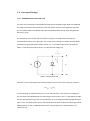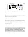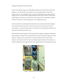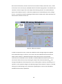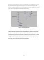
1
ENG460 ENGINEERING THESIS FINAL REPORT PV Array Simulator Performance Evaluation Joshua Yong Ern, CHAN 2011 A report submitted to the School of Engineering and Energy, Murdoch University in partial fulfilment of the requirements for the degree of Bachelor of Engineering. Declaration I declare that this thesis is my own account of research and contains as its main content work which has not previously been submitted for a degree at any tertiary institution. ……………………………………………………. Joshua Chan 18/11/2011 i Academic Supervisor endorsement pro forma This is to be signed by your academic supervisor and attached to each report submitted for the thesis. I am satisfied with the progress of this thesis project and that the attached report is an accurate reflection of the work undertaken Signed: Date: ii Abstract This dissertation evaluates the performance of a 25kW PV Array Simulator based on a design from Prof. Heinrich Haberlin and his staff from the PV laboratory of the Berne University of Applied Sciences, in Burgdorf, Switzerland. The simulator was set up and is operated by ResLab, based at Murdoch University. The device has a power rating of 25kW, an open circuit voltage of up to 750V, and a short circuit current of up to 40A. The design and concept of the simulator replicates the operations of an actual PV array. Incorporated in its controls are eight IV curves of different fill factors that were configured to portray different cell technologies. The development of such a test device was initiated when PV applications such as inverters required a device that could repeatedly produce consistent testing conditions, as well as a platform that could perform precise MPPT measurements. First the study goes into understanding the control options of the simulator in terms of its IV curve production abilities. The initial familiarization stage was conducted with technical manuals and a brief session with Andrew Ruscoe who was involved in the development of the simulator. Through that and further research, it was comprehended that the Main Control, which is the control responsible for all IV curve generations, is designed electronically to follow the single diode model circuit of the PV array. A mathematical aspect has been included in the thesis to confirm the operation of Main Control. Designers of the simulator expanded on this theory by utilising individual sets of diode strings with different configurations, which developed certain fill factors when a voltage is applied. Operation of the PV Array Simulator commenced after the understanding of the controls was established. The eight IV curves of varying fill factors were captured and observed. As part of the study, the curves were classified against the three most common cell technologies. The performance of the simulator was evaluated using different test conditions to observe its stability. It was proven through these tests, as well as documentations from past tests that the simulator was very stable even when it was made to operate at its threshold limit. As the varying fill factors were obtained by the different configuration of diode strings, a study was focused on developing a basis or pattern associated with the formation of different classifications of diodes in series. The diode strings found in the simulator were replicated and reverse engineered. iii Acknowledgements I would like to sincerely acknowledge and thank the following Murdoch staff: Associate Professor Graeme R Cole, my supervisor for his continuous guidance and inspiration Dr Martina Calais, my associate supervisor for her constructive feedback and assistance. Andrew Ruscoe, who took the time to help me with the familiarization of the simulator. Will Stirling and Jeff Laava, for the constant technical support. And my family and friends who have supported and encouraged me throughout my degree. iv Contents Declaration ......................................................................................................................................i Academic Supervisor endorsement pro forma .............................................................................. ii Abstract ......................................................................................................................................... iii Acknowledgements....................................................................................................................... iv List of Figures: .............................................................................................................................. vii List of Tables: .............................................................................................................................. viii Acronyms ...................................................................................................................................... ix Symbols ......................................................................................................................................... ix Chapter One – Introduction .......................................................................................................... 1 1.1 - Background ....................................................................................................................... 3 1.1.1 - Initiative of the PV Array Simulator ........................................................................... 3 1.1.2 - The 25kW PV Array Simulator ................................................................................... 3 1.2 - Concept of Design ............................................................................................................. 4 1.2.1 - Fundamentals of the solar cell................................................................................... 4 1.2.2 - How the PV array simulator simulates a PV array ..................................................... 5 1.3 - Objectives ......................................................................................................................... 6 Chapter Two - Familiarisation with PV array Simulator ................................................................ 8 2.1 - Current Control ................................................................................................................. 9 2.1.1 - Current Source blocks (CSB) ...................................................................................... 9 2.1.2 - IQ 750 CSB Current Source Circuit ............................................................................. 9 2.1.3 - CSB Control Circuit ................................................................................................... 10 2.2 - Main Control ................................................................................................................... 10 2.2.1 - Voltage divider & filter............................................................................................. 12 2.2.2 - Op amp & digital pot ................................................................................................ 12 2.2.3 - Array short circuit current ....................................................................................... 12 2.2.4 - Diode string MUX ..................................................................................................... 12 2.3 - Supervisory & Operational Control................................................................................. 14 2.3.1 - Labview Control Software ........................................................................................ 14 2.3.2 - Field Point Units ....................................................................................................... 14 2.4 - Diode Strings PCB............................................................................................................ 16 2.4.1 - Diode Strings Configuration ..................................................................................... 17 v 2.5 - Mathematical analysis of Main Control .......................................................................... 19 2.5.1 - First contribution to I ............................................................................................... 19 2.5.2 - Second Contribution to I .......................................................................................... 20 2.5.3 - Final Product ............................................................................................................ 23 2.6 - Familiarization and Service of the DC genset ................................................................. 24 2.6.1 - Operating the DC genset .......................................................................................... 25 2.6.2 - Maintenance ............................................................................................................ 28 Chapter Three - Operation of the PV array simulator ................................................................ 32 3.1 - Modes of Operation........................................................................................................ 32 3.2 - Producing And Recording of IV curves ............................................................................ 34 3.2.1 - Acquired IV curves from the PV simulator............................................................... 37 3.2.2 - Classification of the IV-curve options to various cell technologies ......................... 39 3.3 - Investigation of repeatability of tests under different conditions ................................. 40 3.3.1 - Time Drift Test ......................................................................................................... 40 3.3.2 - Temperature Test .................................................................................................... 41 3.3.3 - Further Analysis ....................................................................................................... 42 Chapter Four - Analysis of the IV curve production .................................................................... 45 4.1 - Confirming the operating range of the diode strings ..................................................... 47 4.1.1 - Replicating the amplification control....................................................................... 47 4.1.2 - Measurement of Voltage and Current across the diode strings PCB ...................... 49 4.2 - Diode physical test .......................................................................................................... 51 4.2.1 - Individual diodes ...................................................................................................... 52 4.2.2 - Diode Strings ............................................................................................................ 57 4.3 - Mathematical confirmation of the controls of the PV simulator ................................... 59 4.4 - Duplicating physical tests in LTspice ............................................................................... 62 4.4.1 - Single diode test....................................................................................................... 62 4.4.2 - Diode string test ....................................................................................................... 64 Future Work ................................................................................................................................ 65 Conclusion ................................................................................................................................... 67 Appendices.................................................................................................................................. 68 Appendix A: Replicating the amplification control ................................................................. 68 Appendix B: Measurement of Voltage and Current across the diode strings PCB. ................ 70 Appendix C: Individual diode and diode strings IV curve characteristics test ........................ 72 Appendix D: Screenshots of LTspice simulation ..................................................................... 74 Appendix E: The CD Contents ................................................................................................. 75 vi Bibliography ................................................................................................................................ 76 List of Figures: Figure 1 - Circuit of a solar cell ...................................................................................................... 4 Figure 2 - System Control layout ................................................................................................... 9 Figure 3 - Circuit diagram of the IQ750....................................................................................... 10 Figure 4 - Main Control layout .................................................................................................... 11 Figure 5 - 1N962 zener diode between anode and cathode of selected diode string................ 13 Figure 6 - Diode strings PCB ........................................................................................................ 17 Figure 7 - Circuitry depicting first contribution to I .................................................................... 20 Figure 8 - Circuitry depicting second contribution to I ............................................................... 22 Figure 9 - The Field Power Supply (Left) and the DC GENSET FIELD SUPPLY output (Right) ...... 25 Figure 10 - PV Simulator Input/DC Genset Output Panel ........................................................... 26 Figure 11 - DC Genset AC circuit breaker(Left) and DC Genset DC circuit breaker (Right) ......... 27 Figure 12 - DC genset air filter .................................................................................................... 29 Figure 13 - AC motor (Left) and DC genset (Right) grease outlets .............................................. 30 Figure 14 - Voltage measurement of a capacitor ....................................................................... 31 Figure 15 - States of the PV simulator ........................................................................................ 32 Figure 16 - Physical connection during the setup ....................................................................... 34 Figure 17 - Current Source Blocks ............................................................................................... 35 Figure 18 - Labview user interface .............................................................................................. 36 Figure 19 - IV curve tracer used for the test ............................................................................... 37 Figure 20 - IV curves acquired from the PV simulator ................................................................ 38 Figure 21 - Time Drift Test for Curve 4........................................................................................ 40 Figure 22 - Temperature Test for Curve 4................................................................................... 41 Figure 23 - IV curve of Test 2 ...................................................................................................... 44 Figure 24 - Zoom ins of current ripple ........................................................................................ 44 Figure 25 - Zoom ins of power ripple .......................................................................................... 44 Figure 26 - Circuit depicting the limited voltage applied on the diode strings........................... 47 Figure 27 - Circuit of the amplifying test .................................................................................... 48 Figure 28 - Circuit of diode strings in the test ............................................................................. 49 Figure 29 - IV curve with broken connection .............................................................................. 50 Figure 30 - Connection for the forward biased diode................................................................. 52 Figure 31 - Connection for the reverse biased diode ................................................................. 52 Figure 32 - IV curve of 1N4148 diode ......................................................................................... 54 Figure 33 - IV curve of BZX79C6V8 diode ................................................................................... 55 Figure 34 - IV characteristics of individual diodes ...................................................................... 56 Figure 35 - Experimental setup for diode strings ........................................................................ 57 Figure 36 - IV curves of diode strings .......................................................................................... 58 Figure 37 - Calculated IV curve of the diode strings ................................................................... 61 Figure 38 - Physical test And SPICE simulation of 1N4148 diode ............................................... 62 vii Figure 39 - Physical test And SPICE simulation of BZX79C6V8 diode ......................................... 63 Figure 40 - Connection diagram of the AD826 & set-up circuit .................................................. 68 Figure 41 - Voltmeter connection leads...................................................................................... 70 Figure 42 - Ammeter connection leads ....................................................................................... 70 Figure 43 - Connection for forward biased diode (Left) Connection for reverse biased diode (Right).......................................................................................................................................... 73 Figure 44 - LTspice simulation of 1N4148 diode ......................................................................... 74 Figure 45 - LTspice simulation of BZX-C6V8 Zener diode ........................................................... 74 List of Tables: Table 1 - Field Point Units and their functions............................................................................ 15 Table 2 - Layout of diode strings ................................................................................................. 17 Table 3 - Diode strings voltage drop ........................................................................................... 18 Table 4 - Simulator output of the 8 IV curves ............................................................................. 37 Table 5 -Classification of the IV-curve options to various cell technologies .............................. 39 Table 6 - Results of Temperature Test ........................................................................................ 43 Table 7 - Individual diodes .......................................................................................................... 72 viii Acronyms CSB – Current Source Block. FAULT – This depicts an over-heating or fuse failure condition of the CSB. FPU – Field Point Unit. LIMIT – This would appear as the current output is limited during a fault due to an excessive voltage drop over the CSB. LTspice – Design simulation tools for electrical circuits. MPPT – Maximum power point tracking PV – Photovoltaic RESLab – Renewable Energy Systems Test Centre. Symbols – The DC input voltage to the PV array simulator. This voltage is supplied from the DC genset. –The DC output voltage of the PV array simulator. This voltage supplies the DUT. – Current across the diode. – Current derived from solar radiance. – The short circuit current of the IV curve that is simulated by the PV array simulator. – The current source control signal. This is the signal that is fed through the CSBs. – The open circuit voltage of the IV curve that is simulated by the PV array simulator. ix Chapter One – Introduction This project studies the capability of a PV array simulator that was developed by Prof. Haberlin and his staff at the Berne University of Applied Sciences in Burgdorf, Switzerland. The simulator has a power rating of 25kW, an open circuit voltage of up to 750V, as well as a short circuit current of up to 40A. In addition, there are eight different IV curve options with different fill factors available for selection. The development of the simulator was initiated for the testings of PV applications such as inverters or MPPT charge controllers. These tests were initially conducted on physical PV arrays. However, there were issues associated with these types of tests. Firstly, outputs from an actual PV array are dependent on environmental conditions. Shadings, temperature differences, and different irradiance levels affect the performance of the cell. Therefore, consistent repeated readings cannot be measured. In addition, as inverters were improving rapidly in terms of their efficiency, more precise MPPT measurements were needed. With RESLab’s 25kW PV array simulator, an efficient and steadier platform was realised for all testings of PV applications. The tests or studies can also be conducted in a controlled environment which makes it possible for consistent repeated outputs. Chapter One of the thesis explains the concept behind the design of the simulator. (1) To evaluate the simulator, three main tasks were formulated and discussed in the thesis. The first task involves the familiarization of the controls of the simulator and an understanding of how the IV curve production is achieved. This is crucial for the smooth operation of the simulator. A mathematical analysis was conducted to understand the Main Control. This information, as well as the other controls and components associated with the curve production abilities of the simulator, is presented in Chapter Two. This chapter also discusses the simulator’s Labview control software and the familiarization with the DC genset. The operation of the simulator was conducted as the second task of the thesis. During the operation, the different IV curve options of the simulator were produced and captured. Each curve was classified under the three main cell technologies (Monocrystalline, Polycrystalline, and Amorphous). Performance of the simulator was also analysed to observe any discrepancies in the test results when different test conditions were inflicted on it. These findings are presented and analysed in Chapter Three. 1 It was realised that the varying fill factors in each IV curve option were due to the configuration of diode strings within the PV Array Simulator. Therefore, an array of tests and reverse engineering was conducted on the strings to find out if there is a basis or pattern that is associated with the fill factors. LTspice was also utilised as part of the study to compare physical test results against simulated ones. The final results obtained from the diode strings were inserted into a mathematical equation acquired from the Main Control to confirm that the correct understanding was established. Chapter Four presents the outcomes of the study. This thesis also discusses the possibilities of improving the current IV curve production functions by introducing a digital IV curve circuit. As this has already been looked into during the development of the simulator (1), several modifications have already been made on the control PCB. Therefore, the next step would be to implement and commission the new circuit. 2 1.1 - Background 1.1.1 - Initiative of the PV Array Simulator The Photovoltaic industry is growing rapidly with a great amount of research and development dedicated to the technology. With consumers gaining interest in solar power, and with more of it being introduced into the grid, a greater demand is placed on the quality of the system. It is a known fact that the efficiency of a particular system does not rely on the solar panel technology alone. In fact, it is reliant on inverters to perform conversion from DC to AC as well as to acquire the maximum possible power from the panel. An apparatus was therefore needed to test inverters for their performance under different test conditions. (2) 1.1.2 - The 25kW PV Array Simulator With a power rating of up to 25kW, an open circuit voltage up to 750 Volts and a short circuit current of up to 40 Amps, the PV array simulator offers up to eight different IV curves and allows the testing of a wide range of grid connected inverters or similar applications in a controlled setting. (3) The simulator uses a control PCB which utilises National Instruments Field Point Units to communicate with a Labview programme to simulate solar panels of different types and power ratings. Initially, operation of the PV array simulator was conducted by members of RISE and Murdoch University. However, since RISE has vacated the premises, the building as well as several test equipment were left behind for the use of the University. All the equipment have been transferred to the School of Engineering and Energy in Murdoch University. 3 1.2 - Concept of Design 1.2.1 - Fundamentals of the solar cell The solar cell is essentially a semiconductor diode that is exposed to light. Both cell and diode are made of the same material (silicon) and have similar structure and properties, therefore the one diode model circuit below represents the fundamentals of how solar cells generate electricity. (1) (4) The equivalent circuit of the solar cell (shown in Figure 1) is comprehensive enough to understand the theory of its operation. The current source which is in parallel with the diode simulates the light generated or photo current, . represents the current through the diode. is the resultant output current. V is the terminal voltage. (4) Figure 1 - Circuit of a solar cell Kirchhoff’s current law depicts the resultant output current of the solar cell by the equation: A cell technology is characterized by its IV curve and therefore, a set current and voltage are the two factors that differentiate one technology from the other. The current that occurs during a short circuit, while the is the largest possible is the largest possible voltage during an open circuit. The diode quality factor, which portrays how close the diode is following the ideal diode equation, is also an additional factor that is responsible for the representation of a certain cell. (4) 4 1.2.2 - How the PV array simulator simulates a PV array To simulate a PV array, the characteristic of the cell technology was explored. For the PV array simulator, a DC generator is used to supply power. The desired amount of current source breakers (this is activated via breakers among ten current sources) is first adjusted based on the anticipated that the user wants to set. The precise labview interface. To produce is then selected through the , the input of the DC genset is fed through several control circuits which then generates the simulator’s output voltage. This output voltage can be finetuned via the labview interface and is fed into the device under test (DUT). The DUT adjusts the operating voltage and likewise, a voltage that is proportional to it is fed into the diode strings. The simulator offers up to eight different diode strings, which means that different IV characteristics can be simulated with the desired 5 and . (1) 1.3 - Objectives Objective 1: Familiarization with the PV Array Simulator and its control options in terms of I-V curves produced. This objective involves the familiarization of the PV simulator in terms of its set-up, operation, and its control option in terms of IV curves produced and includes familiarization with the available documentation and technical manuals. Detailed analysis of the system controls to understand the principle of operation. In addition, the Labview control software would also be discussed. The university also arranged for Andrew Ruscoe who was involved with the development of the RESLab simulator to conduct a brief introductory session on the operation of the PV simulator. The aim of this session was to demonstrate the principle of operation of the simulator as well as the basic functions of the simulator. Clear documentation of the findings for the future use of students and academic staff. Objective 2: Operation of the PV Array Simulator and Comparison of results under different test conditions. With theoretical knowledge gained from the familiarization, the next objective was to learn how to operate the PV simulator within the safety ratings acquired from the technical manuals. This includes the generation and recording of IV curves An evaluation of the operation under different test conditions on the array. Selection of different options of measurement after consultation with the supervisor. The simulator requires power input from a DC genset that is connected to a field power supply. The study covers the familiarization, and includes the documenting of the maintenance procedure of the power-generating device. Additional equipment involves the IV curve tracer, which is utilised to set the IV curves. Likewise, a familiarization must be conducted prior to the use of the IV curve tracer. Classification of the IV curves produced by the PV array simulator to various cell technologies. 6 Objective 3: Analysing the operation of the IV curve production of the PV Array Simulator The initial objective set asked for a comparison between the IV curve results generated from the PV simulator against the IV curves of physical arrays. However, through subsequent analysis of the simulator, it was realised that there was no basis to compare results produced by the simulator against outputs from physical cells (the simulator’s main function is to generate IV curves of varying fill factors and does not offer additional possibilities to realistically simulate a particular panel). Therefore, with the discretion of Associate Professor Graeme Cole, the focus was shifted to the study of the operation of the diode strings installed in the simulator. Determination of an operating range for the tests by replicating certain components of the controls. Tests to observe the behavioural aspects of individual diodes as well as selected diode strings. The application of the simulation software LTspice and comparison of simulated results and test results. 7 Chapter Two - Familiarisation with PV array Simulator Familiarization of the PV array Simulator was prepared with the available documentation, manuals, as well as a visit from Andrew Ruscoe, who was involved in the development of the RESLab PV array simulator. Prior to his visit, the PV Simulator Software Specification & Description (1) was utilised to understand the controls that were needed to operate the simulator. It is understood that the System Control acts as a control platform for the simulator. Within the System Control are three different controls. They are respectively the Current Control, Main Control, and Supervisory & Operational Control. Their positions within the System Control are displayed in Figure 2 below. (1) The Labview programme PVSimulator v7, which is the user interface, was located on the RISE network drive and was uploaded to a computer nearest to the simulator for ease of use. A configuration was also done to adjust for the correct settings so that the Field Point Units would be able to communicate with the computer. (1) The overall operation of the simulator involves the initial application of (DC input voltage to the PV array Simulator) through the CSBs. A 50V voltage drop occurs across the CSBs, and the resultant voltage (DC output voltage of the PV array Simulator) is fed into the DUT. The DUT determines the PV array Simulator voltage that is adjusted before being fed back to a selected diode string in Main Control. In addition, the Main Control generates a user defined short circuit current and subtracts the diode current from it. A current source control signal, , is then generated (also from Main Control) and passed through to the current source blocks which is ensured by Current Control. The Supervisory & Operational Control controls and monitors the operation of the simulator. The details of each control are documented in the following sections. (1) 8 1 HVin(+) CB3-CB12 CSB1-CSB10 Supervisory and Operational Control Vin Vcscs Control Main Protection FPUs HVout(+) CB1 CON1 2 Vout CB2 PC HVout(-) HVin(-) CON2 Figure 2 - System Control layout (1) 3 2.1 - Current Control Title A3 Size Da te: File : The Current Control is the lowest level of control in the System Control. Its main function is to Nu mber 4 is passed through to the current source blocks (CSB). (1) 2.1.1 - Current Source blocks (CSB) Rev ision 11- Jan-20 06 She et o f L:\E quipm ent I nform ation\. .\Sy ste m Co ntrol_Dra P_110 wn 106.Sc By : h ensure that the correct current, which is defined by the current source control signal ( Within the simulator are 10 CSBs, which are arranged in parallel. Each CSB produces 4A and consists of ten 0.4A current source PCBs that are mounted on a heatsink. For the implementation of the current control, these current sources are arranged linearly and each controls each individual CSB. (1) 2.1.2 - IQ 750 CSB Current Source Circuit There are ten IQ750s current source circuits within each CSB. A circuit diagram of the IQ750 in Figure 3 displays a voltage follower operational amplifier followed by a transistor at its output. The current source control signal ( is fed into the input of the voltage follower operational amplifier. A transistor at the output acts as a current controlled switch. Voltage across RS shown in the circuit controls the current output of the simulator. For each CSB used, a multiple of ten stages are engaged. (1) 9 F E D C B A contains an operational amplifier and transistor. A dedicated control PCB (CSB Control Circuit) Figure 3 - Circuit diagram of the IQ750 (1) 2.1.3 - CSB Control Circuit The CSB Control Circuit controls the ten IQ750s on each CSB by relaying the input into each of them. Throughout the operation, the IQ750s communicate by sending feedback of their statuses to the circuit. Besides that, the control circuit also monitors the overtemperature switch as well as the voltage drop across the CSB. In the event of a fault across any of the IQ750s, over-temperature or if the voltage drop across the CSB is beyond the normal range, the circuit would perform a control measure by limiting the input which would reduce the output current. The circuit would also send a FAULT or LIMIT signal to the supervisory control. (1) 2.2 - Main Control Main Control of the simulator represents the second level of control and consists of several stages that collaborate to generate the IV characteristics output of the PV array simulator. It does so by monitoring the output voltage of the simulator and adjusting the current source control signal to be at the correct range to produce the desired IV curve. (1) 10 Figure 4 outlines the structure of the main control. When the simulator feeds a positive voltage back into the simulator, the output that is generated becomes negative with reference to ground. This negative output is first fed into the Voltage divider & filter. This ensures that the voltage range is compliant with the controls for the next stage. The output is then passed through to the Op Amp & Digital POT where the fine tuning process of the voltage output (which is adjusted through the Labview interface) is achieved by the control of a digitally selectable gain. In addition, the operational amplifier in this stage inverts the negative voltage input into a positive one. This positive voltage ( string, and a resulting current ( ) is fed into the selected diode ) is generated. The final stage of this control subtracts from a continuously drawn current representing the user’s input array short circuit current ( ). This inverses the signal from the previous stage and thus display a PV array’s IV curve. These stages are explained in detail in the following paragraphs. (1) Figure 4 - Main Control layout (1) 11 2.2.1 - Voltage divider & filter The output voltage from the simulator can be varied over a very large range and therefore needs to be adjusted to fit into the correct range that the controls are utilising. To achieve this, is passed through a voltage divider where a proportional signal is generated. The dividing ratio of the voltage divider is automatically referenced against the which is the voltage proportional to the DC genset’s input . (1) 2.2.2 - Op amp & digital pot For this stage, a 10k digital potentiometer is used to vary the gain of the operational amplifier in the control. The gain is adjusted by toggling of resistance (displayed as programme) which fine tunes the input to the desired in the labview value. This is done while the PV array Simulator is operating in open circuit, and the gain is adjusted to obtain . In addition, the signal is inverted from a negative to a positive value in preparation for the next stage. (1) 2.2.3 - Array short circuit current The is the simulated array short circuit current that is being supplied via the FPUs for the simulator. It is first generated as a current where it is converted into a proportional voltage; so that it can be an input signal to the control. The signal is then fed into an isolation amplifier for isolation, scaling, and inversion. This creates another voltage that is proportional to the original and is continuously drawn into the next operational amplifier; so that a mathematical operation (subtracting of ) can take place to generate an IV curve. (1) 2.2.4 - Diode string MUX There are 8 diode strings available for selection in the Labview interface. Each string produces an IV curve of a certain fill factor. In the “Tune” mode of the software programme, when the user selects a diode string, a multiplexer is employed to connect the desired diode string anode. The cathodes of the diodes are common. (1) 12 In addition, a 1N962 Zener diode with a reverse breakdown voltage of 11V is placed parallel to the diode strings as shown in Figure 5. The purpose of this diode is to ensure that an IV curve would still be generated even without the diode strings. A test that was done to verify the IV curve of this diode is documented in Section 4.1.2. (1) . Figure 5 - 1N962 zener diode between anode and cathode of selected diode string (1) 13 2.3 - Supervisory & Operational Control 2.3.1 - Labview Control Software This control is the final level of control and contains the Labview software that manipulates and monitors the system. In addition, the Labview software allows the user to fine-tune , , as well as the selection of the IV curve. To achieve this, the Supervisory & Operational Control utilises Field Point Units for communication between the system as well as a monitoring platform. 2.3.2 - Field Point Units The National Instruments Field Point Unit is physically located at the bottom of the PV array simulator. For the FPUs to interact with the dedicated computer through Labview, it must be connected via a communication cable. The FPUs include a communication module, as well as six other analog and digital modules. Details of their functions are stated in the table below. (5) 14 Table 1 - Field Point Units and their functions (1) FPU No. Functions FP0 Communication module. FP1 & FP2 Monitors the heatsink temperature of the CSBs as well as the temperature inside the cabinet of the PV simulator. The corresponding temperatures are displayed under “Temperatures” in the Labview programme. FP3 & FP4 Monitors the CSB control circuit and detects any FAULT or LIMIT. The shutdown and diode selection status are being sensed as well. A status display is made available in the Labview programme for each CSB. FP5 Monitors the simulator’s output current as well as its input and output voltage. These are respectively displayed as FP6 , , and on the Labview interface. Allows the user to select the IV curve output of the PV simulator via the Labview programme. The user has to toggle the produce which would then adjust the gain to . This Field Point Unit controls the state of the simulator as well. (eg.Run,Tune,Stop) 15 2.4 - Diode Strings PCB The diode strings which are used for the IV curve production are situated on a PCB. Looking at Figure 6, it can be seen noticeably that there are 8 strings of diodes in series. Each string represents a curve that would be produced by the PV array simulator. Two of the strings had only Zener diodes connected while the other six strings had forward biased diodes in the combination. (1) At the end of each string, metal links are installed to keep the current loop to the minimum length. This is done for the purpose of keeping the induced noise of the circuit to the minimum. From String 1/Curve1 in Figure 6, it can be observed that the first 6 diodes are installed in reverse (as opposed to the overlay) as they are supposed to be reverse biased during operation, while the last diode is installed forward biased. (1) The PCB is interchangeable and other versions of the board can be created by soldering different combinations of diodes. With different combinations, 8 new curves can be created for testing. (1) Further improvements have been made in terms of the production of the generation of curves, and a digital IV curve has now been realised. However, the only available documentations are in the German language and therefore limited information can be obtained from it until a translated copy is obtained. (1) (6) 16 Figure 6 - Diode strings PCB 2.4.1 - Diode Strings Configuration The diodes that were configured in the 8 strings are identified in Table 2. Zener diodes are marked in blue, the forward biased diodes in red, and the links are in black. “IR” means that the diode is installed reversed or against the polarity. The normal operating function of a zener diode is in its reverse region and therefore is commonly installed reversed. Table 2 - Layout of diode strings 17 The breakdown voltages of the Zener diodes can be identified by looking at the last three figures of the serial number. For example, a BZX79C2V7 and BZX79C3V0 diode would break down at 2.7V and 3.0V respectively. Apart from the orange LED that has a forward voltage drop of 2V, the forward biased diodes all have a voltage drop of 0.7V, while the links do not contribute to any drops. The total voltage drops for each curve is calculated and displayed in the table below. (7) (8) (9) (10) (11) Table 3 - Diode strings voltage drop String No. Diode string voltage drop 1 ( 2 ( ( 3 4 ( 5 6 7 8 18 2.5 - Mathematical analysis of Main Control The following section probes deeper into the understanding of a portion of Main Control. To achieve this, the schematics associated with the control were analysed and studied in detail. Design of the control was based on manipulating two set of currents which are associated with the theory of the one diode model of a solar array (theory is documented in Section 1.2.2). The control does this by drawing continuously a user-defined voltage which is proportional to and subtracting the current through the diode strings (this current is also represented by a proportional voltage). Through these circuits, the current and voltage were generated for the IV characteristics of the curve. Figure 7 and 8 displays the circuitry of the operation. (1) 2.5.1 - First contribution to I Figure 7 displays how the first contribution to the resultant current is achieved. This first contribution acts as the and is set by the user through the labview programme. The circuitry is separated into four parts and is numbered in Figure 7 below. An actual copy of Main Control calculations performed by Dr Martina Calais is available electronically in the Appendix. 1. Firstly, a positive voltage that has been adjusted to be proportional to the set is fed into stage 1 (shown in Figure 7). 2. This output voltage is fed into the negative terminal of an operational amplifier (between Step 2 and Step 3). 3. The operational amplifier inverts and amplifies the input. The operation is portrayed by the simple equation below. ( As it can be seen in Equation [2], the product voltage of the initial input is simply a proportional . 19 4. This stage depicts the final output current of the addition of and (details of contribution II are documented in the following section). For every CSB that is being utilised, ten IQ750s are employed. Each IQ750 is calculated as a m stage and is multiplied in accordance to the number of CSBs selected. The equation for the operation is shown in Equation [3]. At this stage, the output current is obtained by dividing the resultant voltage with resistor RS. Depending on the CSBs utilised (1CSB= 10 IQ750s = 10 m stages), a multiplication factor is acquired. The output current depends on how many CSBs are utilised. Figure 7 - Circuitry depicting first contribution to I 2.5.2 - Second Contribution to I Figure 8 explains the second contribution to I. This contribution is the current that goes across the diode strings. The circuit below is separated into five parts. 1. The input V is the input voltage of the DUT. Prior to this stage, the actual voltage that is coming from the DUT would have already been through Voltage divider & filter. Therefore, V is just the signal that is in proportional to the actual. 20 2. V is reduced (using voltage divider rule) and its polarity inverted to produce V3. The equation of this operation is shown below. 3. V3 is fed into the positive terminal of an operational amplifier. This operation does not introduce any gain or inversion and it is believed that buffering occurs at this stage. Therefore, the input and output are equal. 4. V4 is fed into the negative terminal of an operational amplifier with an electronically controlled gain. The resistance R6 consists of a fixed resistor in series with a potentiometer that can be adjusted by the user via Labview. The adjustment controls the gain of the output of the operational amplifier and with that, the voltage across the diode strings V5. The equation depicting this operation is displayed below. 5. Rearranging and expanding of the above equation would display the relationship between the initial input V and VD, the voltage across the diodes: ( ) In addition, V5 sets the voltage across the diodes and the diode current flows through R7. The signal is fed into the negative terminal of an operational amplifier. 21 6. is calculated as the inversion of the diode current across R2. This generates a voltage component for the simulator and is displayed as the equation below. ( An additional factor (number of diodes) is included in this diode equation as there is more than one diode in each string. typically ), is the diode’s saturation current or scale current (this is is the voltage across the diode, (usually 1 or 2 for silicon diodes), is the quality factor of the diode is the thermal voltage (approximately 25mV at 20°C). (12) 7. The current across the diode string in terms of the number of CSBs operated can then be calculated from the equation below. ( V6 is the product of buffering of and for this calculation they are considered to be equal. Figure 8 - Circuitry depicting second contribution to I 22 2.5.3 - Final Product The PV array simulator simulates the currents by working with proportional voltages. The simulator is controlled by V1 (voltage that is proportional to ) and V (feed-back from the DUT and applied across the diode string). These two signals pass through an operational amplifier where V is subtracted from V1. This is in accordance to the PV array circuit diagram where: The theory explains that the resultant output current of the PV array, is the subtraction of the diode current from the generated current. Detailed documentation regarding the operation of PV arrays is included in Section 1.2.2. The simulator translates these currents into voltages so that it can be fed into the controls of the circuitry. An equivalent equation is compiled. ( ( )) V2 is a voltage that is proportional to the output current of each IQ750. Therefore in the equation above, it can be seen that the voltage applied across the diode strings (the DUT sets the voltage range) influences the value of the output current in the desired way. 23 2.6 - Familiarization and Service of the DC genset The PV Array Simulator requires a high DC input for simulating solar panels in operation. A large variation of voltages is required, and the only equipment that can provide a high enough output in the university is the DC genset situated at RISE. It can produce a maximum current of 88A and a DC voltage of 800V, which powers the PV Array Simulator so that it has a maximum current of 40A, and voltage of 750V. Power generators generate power based on the occurrence of electromagnetic induction. Firstly, current is fed into the field coil of the generator creating a magnetic field. When a conductor moves through the magnetic field, an electric current is generated. An armature, which compromises of coil windings on an iron core, acts as the conductor within the electric generator. When the armature is rotated, the coils pass through the magnetic field generating current. With each repeated passes through the field, an AC current is produced as the magnetic flux change through the coils changes at a sinusoidal rate. Therefore, to produce DC outputs, split rings are used to force current to flow in only one direction and in the event rectify the voltage output. (13) (14) A generator does not work independently and requires a prime mover for the rotating of the armature. In this case, a three phase induction AC motor is employed for that purpose. The whole set up which consists of the AC motor and DC generator is referred to as a genset. In this section, details of the operation and servicing of the DC genset that was done in conjunction to the requirements of the project are documented. However, this documentation is not an instruction manual but rather a summary of what was done in the course of the project. There are associated manuals in regards to the operation and maintenance and they are located in the equipment cabinet of RISE. (15) 24 2.6.1 - Operating the DC genset The DC genset is capable of producing up to 800VDC, and utmost precaution must be taken while working on it. As a rule of thumb, no connections should be made while the DC genset is running. Within the DC genset panel (in the engine room), there are four series pairs of 9200uF, 500VDC capacitors. Although they discharge rapidly through the genset windings, a fault might cause large amounts of voltages to remain. Therefore, due care must be taken while replacing or maintaining them. One way of reducing a shock hazard would be to measure the voltage between the capacitors before any work is done. An emergency stop switch is also located at the top of the AC circuit breaker on the DC genset panel. (15) To vary the DC genset output, a field power supply is needed. The field power supply is located on the right hand side of the simulator and is marked “DC Genset Field Supply”. Before any connection is made, the field power supply switch has to be in the “OFF” position and the voltage and current knob are turned completely anti-clockwise (fully reduced). Refer to Figure 9. (15) Figure 9 - The Field Power Supply (Left) and the DC GENSET FIELD SUPPLY output (Right) 25 The PV Array Simulator must then be connected to the DC genset’s output in the “PV Simulator INPUT/DC GENSET OUTPUT” panel, which is located above the “DC GENSET FIELD SUPPLY” output. This is done by wiring the input of the PV Array Simulator to the appropriate sockets. The “DC genset to PV simulator” (the left switch in Figure 10) circuit breaker is turned on to complete the connection. It was noted that the panel was designed to only allow one switch to turn on at one time for safety reasons. The right switch in Figure 10 is “OTHER DC SOURCE to PV SIMULATOR”. For safety, the circuitry has been designed to only allow one switch to be turned on at one time. (15) Figure 10 - PV Simulator Input/DC Genset Output Panel 26 After the field power supply is correctly connected to the DC genset, the DC genset’s AC circuit breaker and DC circuit breaker (on the left and right of the DC Generator Panel as shown in Figure 11) are switched on. The emergency stop button is rotated anti-clockwise to ensure it is not engaged. With this done, the green “start” button is pressed to start the DC genset. It can be observed that the DC genset’s voltmeter above the DC circuit breaker increases slightly. This is normal as the DC genset is expected to run at 4V without a field. (15) Another check is made (a breeze is felt) to ensure that the ventilation fan on the roof is activated upon starting the DC genset. Figure 11 - DC Genset AC circuit breaker(Left) and DC Genset DC circuit breaker (Right) 27 With the field power supply (Figure 9) turned on and connected to the running DC genset, the supply voltage is increased by turning the “V” knob on the left of the field power supply. The “A” knob, or the current control was increased to allow for the appropriate amount of voltage to be fed to the simulator. As the voltage is being increased, the “PV Simulator input/DC genset output” panel was observed for the desired DC voltage input from the DC genset. The PV Array Simulator has a 50V drop across its current sources. Therefore, if 100V is required from the simulator output, 150V must be fed into the simulator’s input via the DC genset. (15) To turn off the DC generator, the field supply is reduced to 0 by turning the “V” knob anticlockwise and switching the supply off. This brings the DC genset’s voltage down to 4V. To stop the motor, the red “stop” button (Figure 11) is pressed. The motor takes a few minutes before coming to a complete halt. (15) 2.6.2 - Maintenance The DC genset must be maintained so that top performance as well as a longer lifespan can be achieved. Currently, maintenance is being conducted by staff of the School of Engineering & Energy on an annual basis. As part of the project requirements, maintenance was conducted under the supervision of Wayne Clarke and documented in the below sections. The steps taken were in accordance to the DC Genset Maintenance Instructions located on the RISE network. The three main components of the maintenance are (16): Checking of the DC genset air filter. Lubrication of the DC generator and the AC motor. Checking the voltages of the capacitor bank. 28 Checking of the DC genset air filer The air filter is located at the front side of the DC generator set. Access was achieved by the removal of the lower 2 and the loosening of the top 2 bolts of the lid which was covering the filter. From Figure 12, it shows that the filter was stained black but it was explained by Wayne Clarke that it was normal. An obstruction test done later showed that the filter was still in a satisfactory state as adequate air flow was felt while the generator was running. With the check done, the appropriate box was checked off in the DC Genset Maintenance Schedule. (16) Figure 12 - DC genset air filter Lubrication of the DC generator and the AC motor The DC generator and the AC motor require annual lubrication with their respective grease. Two separate grease guns with cartridges marked “DC” and “AC” respectively are located in a plastic container inside the engine room. In addition, two spare cartridges are also available. (16) There are two grease outlets each in the DC generator and the AC motor. From Figure 12, the locations of the outlets are shown circled in red. The AC motor’s grease outlets require opening and this can be done by lifting two levers located at the bottom of the outlets. No opening of outlets is required for the DC generator. (16) 29 Figure 13 - AC motor (Left) and DC genset (Right) grease outlets During greasing, the DC genset is then operated without a load. Running the genset ensures that the grease is evenly distributed. With the grease cartridge marked “AC”, 30 full pumps are applied to each of the outlets on the AC motor. Likewise, the grease cartridge marked “DC” is used to pump 10 full pumps on each of the outlets of the DC generator. (16) With both AC motor and DC generator lubricated, the DC genset is left to run for an additional hour. This is done to allow for the expulsion of excess/old grease from the bearings. With that done, the AC motor’s grease outlet is closed and the DC genset shut down. The appropriate box was then checked off in the DC Genset Maintenance Schedule. (16) 30 Checking the voltages of the capacitor bank There are two parallel strings of two 500V 9200uF capacitors connected to the output of the DC genset. In an ideal situation, two capacitors in series would equally share the output voltage. However, over prolonged periods, the capacitor might degrade and display different leakage currents. This would cause voltage imbalance and will cause a failure in the operation of the DC genset. Therefore it is paramount that the voltage across each capacitor is checked annually to verify that it is still operating in the correct voltage range. (16) The four capacitors are located behind the DC Genset panel. As the panel had been designed not to operate with their doors open, a pair of plier was used to manually turn on the DC circuit breaker. This is extremely hazardous as the capacitors will be charged and therefore can only be done by qualified personnel. (16) With the DC genset running without a load, the field power supply was adjusted to 500V (field supply voltage). A voltmeter with a 1000V probe was used to measure the voltages across each capacitor. In Figure 14, the measurement of a capacitor displays 253V across one of the capacitor. This capacitor falls under the correct voltage range of between 220V to 280V. Any capacitor falling out of the range would have to be replaced with the same model number. (16) Figure 14 - Voltage measurement of a capacitor 31 Chapter Three - Operation of the PV array simulator 3.1 - Modes of Operation To efficiently control the simulator’s operation, four modes are programmed and can be controlled via the Labview software. The four modes are STOP, RUN, DEFINE, and TUNE. When the Labview programme is initially started up, (the System Status would be flashing if Labview is connected correctly and the FPUs are operating) the operating mode is STOP. In this mode, the PV simulator is on standby and does not produce any output. In DEFINE mode, the user selects the number of CSBs corresponding to the ones set physically at the PV simulator. The IV curve is also selected in this mode. As the corresponding output voltage would only be approximated, TUNE mode is used to adjust it to the desired voltage. This is achieved by adjusting an operational amplifier with an electronic gain. With all these parameters set, RUN mode is selected and the PV simulator begins to output an IV curve according to the voltage operating range set by the DUT. It must be noted that these procedure is not in order. RUN mode is used multiple times to observe after the adjustment. The correct procedure to operate the simulator would be to select STOP after DEFINE and TUNE has been adjusted before going on to RUN. This enables the simulator to accurately output the desired values. Figure 15 - States of the PV simulator The modes of the PV simulator are depicted in Figure 15. Each mode is programmed to perform a certain task and details of their operation are discussed in the paragraphs below. 32 STOP MODE The DUT is disconnected thus cutting off the feedback input. Main supply coming through the current source outputs are also ramped down to zero. From this point, the user can select either RUN or DEFINE. Selecting RUN would operate the simulator on the defined current settings while selecting DEFINE gives the user the option to set or modify the settings. DEFINE MODE In this mode, the user can set the correct number of CSBs under Define Parameters in the Labview programme. This must be set correctly, as it tells the control how many m stages are being applied. In this mode, the user can also choose from eight different IV curves. SAVE Define Parameters must then be selected to confirm the parameters. TUNE MODE In this mode, the current sources are ramped up to follow the set current selected for the IV curve. However, at this stage, the DUT contractors remain open. This is to allow for the display of (Voltage input from DC generator) and Labview programme. and current sources. Therefore, the (Voltage output of PV array Simulator) in the has a 50V difference due to the voltage drop across the must be adjusted to be 50V larger. The desired then be adjusted under Tuning Parameters by adjusting the Labview. The correct can option and selecting SAVE in will be displayed only after SAVE is selected. RUN MODE When this mode is selected, the DUT is connected and an operating voltage is fed into the simulator. The current sources are ramped up as well to the selected current setting. This puts the PV simulator into operation. If any adjustments are required, the user can select STOP and move on to either DEFINE or TUNE to make changes. 33 3.2 - Producing And Recording of IV curves The completed setup that was achieved and concurrently used for the tests is reflected in Figure 16. AC power is required to run the simulator’s components and must be connected prior to the test. The Labview programme PVSimulator v7, needs to be running prior to any inputs from the DC generator. The Field Power Supply connected to the generator is used for the adjusting of DC voltage. Figure 16 - Physical connection during the setup 34 Before running the DC generator, it must be ensured that the Field Power Supply is adjusted to 0. The required DC output voltage should only be increased after it is running. It must be noted that the current limit (of the Field Power Supply) needs to be adjusted to allow for the unrestricted supply. In addition, the user has to take into account the 50V voltage drop across the current blocks. This means that if the user wants to achieve an open circuit voltage (Voc) of 100V, the DC output voltage (Vdc) would have to be adjusted to 150V. Although there is no danger if this is not followed, an insufficient voltage drop would produce an incorrect output of the PV array simulator. On the other hand, it must be ensured that the user keeps the voltage below the simulator’s rating (750V). (1) (3) Operating the simulator is straightforward with the full set up in place; the user selects the number of current sources which are physically located at the top right corner of the machine. The current sources are arranged in parallel and have output currents of 4A each. Three of the CSBs located in the simulator are shown in Figure 17. In the simulator, there are ten CSBs connected in parallel. Each of them has ten current source circuits (IQ750s) connected in series. Figure 17 - Current Source Blocks 35 Once this has been done, the user sets the correct number of CSBs, selects the curve, as well as the short circuit current (Isc) in DEFINE mode of the Labview programme. The Labview user interface is shown in Figure 18. As the output from the DC generator equal to the simulator input / would initially be without any adjustments, the desired open circuit voltage must be fine-tuned by adjusting the Rvoc while in TUNE mode. These operations are documented in detail in Section 3.1. Figure 18 - Labview user interface In order to capture the curves, a DUT was needed to set the voltage ranges to be applied across the diode strings. In this test, an IV curve tracer was utilised and connected at the output of the simulator. A dedicated software comes with the tracer and operating instructions were obtained from the DS-100C I-V CURVE TRACER User Manual (17). The IV curve tracer obtains the curve by receiving the output from the PV simulator and varying the impedance of the output from zero to infinity which is done by connecting it to a capacitor. As the capacitor charges, the operating range of the simulator’s output is recorded, starting at Isc and finishing at Voc. Information regarding the IV curve tracer (DS-100C) is available electronically in Appendix E. 36 Figure 19 - IV curve tracer used for the test 3.2.1 - Acquired IV curves from the PV simulator Table 4 - Simulator output of the 8 IV curves ( ( ( ( Curve No. Power(W) Fill Factor(%) 1 325.3 3.763 101.228 3.595 90.496 85.4 2 343.5 3.754 113.537 3.546 96.875 80.6 3 347.7 3.763 104.474 3.693 94.155 88.4 4 265.9 3.736 107.120 3.344 79.500 66.4 5 339.7 3.760 100.515 3.699 91.847 89.9 6 278.5 3.754 109.221 3.326 83.741 67.9 7 312.2 3.754 112.130 3.519 88.713 74.2 8 272.2 3.754 111.342 3.299 82.521 65.1 Eight IV curves of varying fill factors were captured using the IV curve tracer. The adjusted and output from the simulator was respectively 100V and 4A for the test. Table 4 displays the outputs from the PV array simulator. It can be seen that eight varying fill factors were produced. Each curve is specifically designed to generate a fill factor that depicts a certain cell technology. Figure 20 depicts the eight different curves that were obtained. 37 Figure 20 - IV curves acquired from the PV simulator 38 3.2.2 - Classification of the IV-curve options to various cell technologies As the simulator is used for the testing of applications associated with PV modules, research was done to attain further information on the cell technology that is being replicated. The table below gives an approximate classification on the fill factors of each cell technology. Using this material, the curves were sorted according to their fill factors. This gives the user additional information when interpreting the results of the test. (18) Table 5 -Classification of the IV-curve options to various cell technologies Cell Technology Fill Factor(%) Curve No. Monocrystalline silicon solar cell 83-86 1,2,7 Polycrystalline silicon solar cell 87-89 3,5, Amorphous silicon solar cell 63-66 4,6,8 39 3.3 - Investigation of repeatability of tests under different conditions As it was not certain how stable the simulator was in terms of its operational stability, the simulator was tested under conditions that might affect its performance. There were namely two different tests that were suggested by Andrew during his visit to RISE; the time drift test and the temperature test respectively. Both tests are explained and discussed in the paragraphs below. 3.3.1 - Time Drift Test This test was initiated for two purposes. One was to find out if the simulator had a “warm-up” period, and if there was a need to run the machine for a certain duration before it could produce an accurate output. The other purpose was to observe if the simulator would produce consistent results over a time period (a few hours), and if there was a time limit in which the simulator could be left running before irregularities occur. The 8 curves were observed and captured every 10 minutes, with 10 tests performed. Once they were obtained, Microsoft Excel was used to arrange the curves for comparison. It was realised that running the machine over a prolonged period did not affect the output of the curves. In addition, the simulator did not require a “warm up” period as well with the first curve identical to the rest of the curves. Figure 21 showing Curve 3 displays the 10 curves. It can be inferred that the outputs were identical and each curve was overlapping the other. An electronic copy of the data collected for the Time Drift Test is available in Appendix E. Figure 21 - Time Drift Test for Curve 4 40 3.3.2 - Temperature Test Similar to most electronic equipment, the performance of the simulator might have the tendency to degrade in higher operating temperatures. Therefore, it was paramount that the curves produced were observed over different temperatures. It was suggested by Andrew that the heating system in the lab be utilised to increase the ambient temperature. As the highest temperature that the heater could attain was 30 degrees, the test was structured for measurements to be taken 3 times with intervals of 30 minutes. Two thermocouple wires included with the IV curve tracer were used to measure the ambient temperature. The three ambient temperatures recorded were 23.8 degrees, 26.8 degrees, 28.4 degrees. It could be seen again that although the temperature varied by approximately 5 degrees from the first and last test, the IV curve output from the simulator was not affected. Figure 22 shows Curve 4 over the three temperatures. It can be derived from the test that the superior stability of the simulator allows the output to be unaffected even when temperature condition changes. Figure 22 - Temperature Test for Curve 4 41 3.3.3 - Further Analysis The time-drift and temperature tests did not suggest any changes to the curves when the simulator was placed under different conditions. It was thus decided that the simulator would have to be stressed, as without any loads involved, the machine would not significantly heat up. It was noted as well through discussions with the supervisor that the ambient temperature should not be the determining parameter. Instead, the internal components of the machine (monitored by FPUs) should have been the varying factors. Initially, there was an attempt to utilise two load banks that were situated at RISE. However, through analysis and calculations of the ratings, it was realised these did not provide a large enough load to be taken into consideration. An initiative was also made to obtain permission to connect the PV simulator to a grid connected inverted. The operation of inverters however exposes the user to dangerous voltages. There was not a suitable candidate that could facilitate the test during the time frame of the project, the attempt was abolished. However, a documentation regarding an acceptance test was obtained through further research. The test demonstrates the stability of the PV simulator in different conditions by using big resistors as loads. A temperature test was performed at the Burgdorf PV laboratory at the Berne University of Applied Sciences during the presence of Dr Martina Calais. She has approved of the documentation of the test in this thesis. (19) (19) The test was conducted in three stages with varying temperatures. Firstly, a test was done at ambient temperature and depicted the simulator under normal operating condition. For the second test, the simulator was intentionally heated up by being made to operate on large resistors for a specified duration. When the heatsink temperature reached 55 degrees (shut down temperature is 60 degrees), the IV curve was recorded. The simulator was then allowed to operate till shut down occurred, and another test was performed at 60 degrees. (19) 42 Results of the three tests are as follows: (19) Table 6 - Results of Temperature Test ( ( ( ( Test No. Temperature( 1 Ambient 757.29 11.502 622.97 7.165 2 55 757.29 11.534 622.24 7.117 3 60 757.32 11.527 622.86 7.180 From Table 6, it can be observed once again that the temperature did not seem to affect the output of the simulator. There was also zoom-ins of the curves that were taken for the Test 2 when the simulator was operating at 55 degrees. Figure 23 displays the I-V and P-V curve of Test 2. Figure 24 displays the zoom ins of the current ripple and it could be observed that the ripple was in the order of 5mA maximum. Figure 25 displays power ripple, and it is within 5W at maximum. Zoom-ins of the curves of the other two temperatures were not included in the document but it was mentioned that the magnitude of the ripples were consistent with Test 2 (55 degrees). (19) 43 Figure 23 - IV curve of Test 2 Figure 24 - Zoom ins of current ripple Figure 25 - Zoom ins of power ripple 44 Chapter Four - Analysis of the IV curve production In electronics, a diode acts like pressured “flow-valve” in an electrical cable. The general usage is to create a blockage and only allows current to pass through if it reaches the diode’s conducting voltage. Diodes are utilised in many electronic circuits and are often used for protection or regulation in a circuit. For a diode to conduct, the magnitude of the voltage applied must be high enough to collapse the depletion region of the diode. A typical silicon diode conducts at approximately 0.7V while forward biased and allows current to pass through in the circuit. If a reverse voltage is applied onto the diode, it does not conduct and creates a blockage. All diodes have a reverse voltage threshold, which is of considerable magnitude (generally 50V and above). However, if the applied voltage goes beyond the breakdown voltage of the diode, a breakdown would occur. Since the diode is not designed to work in that region, it would be damaged. On the other hand, Zener diodes are made specifically to operate in their breakdown region. A Zener diode acquires its properties from a heavily doped P-N semiconductor junction. When a forward voltage is applied, the Zener diode functions like a normal forward biased diode and conducts at 0.7V. On the contrary, if a reverse voltage is applied, the Zener diode allows conduction to occur by operating in its reverse region. (20) The diode has an I-V characteristic and it is explained by the Shockley diode equation: ( where [12] is the diode’s saturation current or scale current (this is typically the voltage across the diode, silicon diodes), ), is is the quality factor of the diode (usually between 1 and 2 for is the thermal voltage (approximately 25mV at 20°C). (12) 45 The first few stages of the Main Control are essential as the input from the simulator needs to be adjusted to fit into an appropriate operating range. However, the simulator’s ability to generate IV curves of varying fill factor lies in the output coming from the diode strings. Since the fill factors are determined by the set of diodes, the purpose for the study is to realise how the IV curves are physically produced by the different configuration of diodes installed in the PV simulator. When that is achieved, an additional incentive would be to learn if there is a way to create a curve of a desired fill factor. As the documentations provided very little information on this aspect of the operation, a study was conducted to confirm the operating range of the diode strings in operation. Once this was achieved, the IV characteristic of a single diode as well as the diode string are explored. The study was conducted in the following order: Confirm the operating range of the diode strings Observe IV curve of an individual diode Observe IV curve of a diode string 46 4.1 - Confirming the operating range of the diode strings Identifying the range was of utmost importance because diodes behave differently when exposed to different voltages and currents. However, there was little or no basis regarding the operating range of the diode strings in any of the available documents. Therefore, to obtain more information regarding this aspect of the operation, two tests were conducted prior to the physical testing of the diodes as an attempt to confirm the range. 4.1.1 - Replicating the amplification control An attempt was made to amplify the voltage across the diode strings as it was believed that very small voltages were used in the controls. The implementation behind this consideration was due to two main reasons. Firstly, the amplifier (bottom operational amplifier in Figure 26) used in the schematic was an AD826AN High-Speed, Low-Power Operational Amplifier. The operational amplifier has an operational voltage of ±15V, which means that the maximum voltage would only be an output of 13.5V (1.5V less than voltage at the rails). Furthermore, a Zener diode (circled in red) with a breakdown voltage of 11V is placed between the anode input and cathode output of the diode strings. This signifies that the voltage range would be approximately 11V at the output. As there were several strings that have a total breakdown voltage of more than 11V, it was inferred that the curve production was occurring before the “knee” of the string’s IV curve. (1) (21) Figure 26 - Circuit depicting the limited voltage applied on the diode strings. (1) 47 Therefore, to understand what the circuit was actually doing, a part of the simulator’s control was replicated as seen in Figure 27. The test was set up to study the output of the U21B operational amplifier in Figure 26. As it was known that the maximum voltage across the diode strings was 11V, the voltage was varied from 0-11V in the test. Figure 27 - Circuit of the amplifying test Curve 1 (One of the curves produced by the PV array Simulator), which had a total breakdown voltage of 18.1V, was tested in this setup. It was realised that no significant voltage change was observed at the output of the operational amplifier when the voltage across the diode string was varied from 0V to 11V. At this point, it still was not clear why there was no reading coming out of the operational amplifier. However, the output result in this test was not imperative because there was now a strong basis of the maximum operating voltage of the control. The test procedure is discussed in detail in Appendix A. 48 4.1.2 - Measurement of Voltage and Current across the diode strings PCB The previous test (Section 4.1.1) did not present an output. However, it was learnt that the operating voltage range would not be higher than 11V due to the contrains presented by the operational amplifier and the 11V Zener diode. Continuing on with the study, another test was devised to realise the actual voltage and current that was applied/passed through the PCB during the curve production. Only then would there be a closure as how the PCB is working with the control system of the simulator. For this test, the connection was broken by slitting the wiring lining on the PCB (This was done for all the strings). This provided an open circuit where two leads for an ammeter was soldered in. The ammeter would be used to measure the current passing through the strings during the curve production. In addition, to monitor the voltage across the string, two leads was soldered over the two points as illustrated in Figure 28. Figure 28 - Circuit of diode strings in the test 49 The simulator was powered up and the IV curve tracer was used to generate a waveform. As the IV curve tracer sets the operational voltage across the string of diodes, an observation was made on the voltmeter and ammeter whilst the tracer was conducting the DC sweep. The first test was conducted with the connection between the input voltage and the seven other strings of the diodes broken. Results for each curve selection through the labview interface displayed an identical curve (same fill factor). By the reading of the schematic, it shows that the signal has went through the diode strings and passed through the zener diode between the D_An and D_Cat (Information of this diode is included in the previous test). Therefore, it has been confirmed that the diode strings share a common cathode and the breaking of the connection between the signal and diodes caused an open circuit. Figure 29 - IV curve with broken connection Figure 29 displays the IV curve when the diode strings were broken. The IV curve has a fill factor of approximately 96% and is generated consistently with each curve number selected when there is an open circuit in the PCB. For the second test, the broken connection for the strings were restored. This time, the eight curves were generated as per normal with their respective fill factors. However, the voltage and current readings were displayed as noises (the current measured was less than 100uA). The test procedure is discussed in detail in Appendix B. 50 4.2 - Diode physical test The Diode physical test was separated into two tests. In the first test, individual diodes that formed the diode strings were tested and compared alongside to observe the basis of their operation. This was done also to observe if the diodes operated according to their stated ranges. After substantial research and confirmation of the previous two tests, the physical diode tests was conducted employing an input voltage of 10V and a limited maximum current of . The operating range for the test was decided after consulting the diploma thesis Der Solargenerator-Simulator (6) (this thesis can be obtained in the Projekt AUS file in RISE) which was completed by students affiliated to the Berne University of Applied Sciences that was involved in the development of the PV simulator. The basis of such a small magnitude was because diodes change their properties when they heat up. Therefore, to attain the accuracy of the test, controlled voltages as well as minimal currents were used to ensure that the temperature was controlled. The second test involved the testing of three selected diode strings. These strings were configured to replicate the diode strings which were used in the PV simulator. (6) 51 4.2.1 - Individual diodes The test was previously conducted with Protek 506 digital multimeters. However, they proved to be unfit for accurate measurement of micro-amps and therefore a higher precision multimeter was employed for the test. Individual diodes found in the diode strings of the simulator were tested to aid in the understanding of their operational behaviour. The diodes were differentiated by forward or reverse biased and have to be installed correctly to produce the correct results. The figures below depict the setup for the test. It can be seen in Figure 30 that the diode is forward biased because the polarity of the DC power source allows for electrons to flow within the diode. In a forward biased configuration, the positive end of the diode is the anode while the negative end is the cathode. Figure 31 displays the diode installed opposed to the polarity of the DC power source and therefore works reversed-biased. Included in the circuit are an ammeter and resistor connected in series, as well as a voltmeter connected in parallel to the diode. Figure 30 - Connection for the forward biased diode Figure 31 - Connection for the reverse biased diode 52 To capture the IV characteristics of the diode, a DC voltage sweep was achieved by manually adjusting the voltage of a DC power source from 0V to 10V. The current was kept at and this was achieved by adjusting the correct resistance for each test. The resistance was toggled according to two main parameters of the diode which are respectively the voltage/current ( ) for forward biased diodes, as well as the voltage/current ( reversed biased diodes. and ) for are then respectively subtracted from the maximum voltage of 10V, to calculate the voltage drop across the resistor. Therefore, to control the operating current of the circuit to , the resistor can be adjusted accordingly. and depicts the diode’s normal operating current and it must be noted that currents higher than the permissible working range should not be applied. However, as the maximum operating current in the circuit was a mere , this was not a concern. The methods and procedure of the test is included in Appendix C. 53 Forward biased diode Figure 32 - IV curve of 1N4148 diode Figure 32 displays the IV curve of a 1N4148 forward biased diode. Like all normal forward biased silicon diodes, the 1N4148 starts conducting close to 0.7V. It can be observed from the steep inclination of the curve that as soon as the voltage reaches the forward voltage drop of the diode, the voltage would remain constant irregardless of the current applied. 1N4148s are mainly used as signal diodes. As signals require only small voltages to operate, the 1N4148 diode with a forward voltage drop of 0.7V is well suited for such operations. (10) 54 Reverse biased diode Figure 33 - IV curve of BZX79C6V8 diode Figure 33 displays the IV curve of a BZX79C6V8 reverse biased diode. The BZX79C6V8 behaves like an ordinary forward biased diode and conducts at approximately 0.7V when it is made to work in the forward region. However, it is designed to specifically to operate in the reverse region and is always installed reversed. The Zener diode starts conducting when its breakdown voltage is met and it can be seen that the BZX79C6V8 diode is breaking down at 6.8V as displayed by the IV curve. When the breakdown voltage is met, the Zener diode limits the voltage of the circuit. Therefore, a Zener diode is used to reduce voltages and is often employed for voltage regulation. (7) 55 Compilation of IV curves of individual diodes Figure 34 - IV characteristics of individual diodes Figure 34 displays the IV curves of 13 diodes that were being used to configure the eight strings located in the PV simulator. It can be observed that for all the diodes tested, the applied voltage is limited when it reaches the rated forward or reverse breakdown voltage of the diode. It can be seen that the each curve portrays an inverted PV array IV curve. It was also clear that each diode had a specific characteristic which meant that curves of different “fill factors” can be generated. 56 4.2.2 - Diode Strings It was observed from the test of individual diodes that each curve provided a specific set of IV characteristics. To continue the study, another test was conducted to observe how diodes behave when they are placed in series. After analysing the diode strings, it was realised that the total voltage drop across the diodes in all of the strings was larger than the input voltage of 10V (more information regarding the voltage drops of the diode strings are included in Section 2.4.1). Diodes require the applied voltage to be higher than the forward or reverse breakdown voltages to allow current flow. Therefore, in theory, if that voltage was not met, the current would not be able to pass through. This led to the consideration that the diode strings were operating low currents close to the “knee” of their IV curves. Due to the fact that the diode strings had a larger voltage drop than the input voltage of 10V, the test current did not reach , which was achieved earlier in the individual diode test. Therefore, the resistance was adjusted to allow for the highest possible current range possible for this test. Figure 35 demonstrates a test being conducted to observe the IV curve on String 7. To adjust the operating current, the potentiometer was used to adjust the resistance for each individual string. Figure 35 - Experimental setup for diode strings 57 Figure 36 - IV curves of diode strings Three strings from the test were selected based on their varying curve characteristics. Looking at the IV curves of String 1, String 3, and String 4 of the diode strings in Figure 36, it can be confirmed that the curves were being produced by currents of very small magnitudes. Both String 1 and String 3 were generated in the range, which was half of the operating range of the individual diode test. The test demonstrates that the designers of the simulator is utilising small currents to generate IV curves. 58 4.3 - Mathematical confirmation of the controls of the PV simulator The Main Control explains that the IV curve production was achieved by subtracting the current across the diode string from the applied short circuit current (these currents are all represented by voltages in the controls of the simulator). Calculations based on formulas provided in Section 4.3 was used to demonstrate how the IV curve of String 4 was used to produce an IV curve mathematically. As the control uses voltages as signals, a voltage that is proportional to the the is generated. As of String 4 was measured to be 3.763A (actual value measured from the simulator after the selection of 4A), the voltage signal V1 can be calculated by the equation (the equations can be obtained from Section 4.3): Where, (1) (3 CSBs were switched on, therefore (reading from the PV simulator) Rearranging the equation gives, As Where, (1) (1) 59 stages) The voltage signal V1 is then inserted into the equation below, where the product current (still in the form of a voltage is calculated): ( Where, ( )) (There are 5 diodes in string 4 ) ( 25mV at 20°C When inserted into the equation, the final current in terms of a voltage is attained. However, as the aim was to display the IV curve in the correct settings, the final current output is obtained by converting the voltage signal voltage signal Where, to current . The relationship between the and is depicted by the equation: (1) (3 CSBs were switched on, therefore stages) Therefore, the final equation is: *[ The only factor that changes is ] ( [ )]+ which is the voltage applied across the diode strings. 60 Figure 37 - Calculated IV curve of the diode strings When the above method of calculation was applied to the three diode strings acquired from the test, the IV curve recorded displayed the essence of a PV array’s IV curve which can be seen in Figure 37. This confirmed the accuracy of the calculations and the understanding of Main Control. These three IV curves however were not similar to the actual curves provided by the PV simulator. This is because the PV simulator draws approximately 200-300 data points to form an IV curve, compared to only 10 data points acquired by the physical test. With the constraint of so minimal data points, and with working ranges in micro amps, an accurate representation of the curve through a physical test was not feasible. The calculation in Excel can be obtained from Appendix E. 61 4.4 - Duplicating physical tests in LTspice 4.4.1 - Single diode test Simulation software LTspice was also utilised as an additional method to observe the IV characteristics of the diodes. Results led to the understanding on how diodes operate and also served as a testing platform before any of the physical tests were conducted. The figures below compare curves attained in the simulation software against the results of the physical tests. Figure 38 - Physical test And SPICE simulation of 1N4148 diode Figure 38 compares the physical and simulated results of the IV curve attained from a forward biased 1N4148 diode. There is a very slight variance between the two results; with a 0.05V difference between the two conduction voltage. LTspice functions by drawing information on the parameters of the diode and simulating the IV curve. As there was only 0.1uA difference between the two curves (SPICE and Physical test), it can be inferred that the 1N4148 model created by LTspice is reasonably accurate. Screenshots of LTspice can be obtained from Appendix D. 62 Figure 39 - Physical test And SPICE simulation of BZX79C6V8 diode Figure 39 compares the simulation and physical tests of the BZX79C6V8 Zener diode in the reverse biased mode. By looking at the curve acquired by the LTspice simulation, it can be observed that conduction occurs at the 6.8V mark. On the other hand, the physical test demonstrates that in actual operation, diodes do not conduct precisely at their breakdown voltages. Similar to the previous comparison, the results from LTspice is very close to the acquired measurement data from the physical test. It can therefore be learnt that LTspice is a useful tool to observe the behaviour of diodes if a physical test was not possible. Screenshots of LTspice can be obtained from Appendix D. 63 4.4.2 - Diode string test LTspice was not able to produce reasonable results when the physical test was replicated. This was because for all of the diode strings, the input voltage was lower than the total breakdown voltage of the diodes in series. This led the simulation software to believe that as the breakdown voltages were not met, the strings would not conduct and allow any current to pass through. In addition, LTspice does not take leakage currents into consideration as it is often neglected in real life applications. Therefore, with the simulator representing no current passing through, there was no possibility of generating any output. 64 Future Work It was concluded that the simulator is very useful and can be utilised for the testing of inverters. However, the limitation of the simulator’s usage lies in the choices of IV curve options. This limits the versatility of the usability of the simulator because it confines the user to only eight different options of fill factors. Such a restriction sets a constraint for the simulator. Therefore, further improvements must be made in the current IV curve generation function. During the development of the simulator, another form of curve generation was realised. This curve generation was in the form of a digital IV curve generation. It was implemented by two students undertaking a diploma thesis Der Solargenerator-Simulator (6)(this thesis can be obtained from the folder marked Projekt AUS situated at RISE) which was written in German. Due to the language constraints, details of how the implementation worked could not be attained. However, there are a few benefits that can be derived from such a technology. The benefits of having a digital IV curve generation are tremendous. The user will be able to simulate any kind of cell technology . This can be done by either conducting an initial physical test to capture the behaviour of the particular cell, or by researching to obtain the characteristics of the panel that needs to be simulated. As the digital IV curve generation is programmable, predictable and accurate results can be obtained as long as the correct cell characteristics are inserted. In addition, different conditions such as shading, different temperature levels, and different irradiance level can be simulated. This will further improve the testability of the ranges of PV applications. There were recommendations discussed in A Stability Discussion for Main Control (located at Appendix P: PV Simulator Technical Manual) that two options be utilised for the IV curve generation. (1) They are the: A/D converter EPROM/EEPROM 65 The A/D converter is a circuit that converts analog data into digital information. Therefore, in the case of the PV simulator, a programmed signal can be passed through to the A/D converter circuit where a digital output would be produced. EPROM or EEPROM means Erasable Programmable Read Only Memory and Electronically Erasable Programmable Read Only Memory respectively. They both serve as programmable memory devices that are programmed electronically and yet can be erased and re-used. The difference between the two is that the former erases its data under UV light, while the latter can erase its data electronically. Benefits of the EPROM/EEPROM are that the user would be able to programme and re-programme the selection of IV curves freely. (22) Both options ease the tedious process of sampling by the configuration of diode strings to produce a certain IV curve characteristics. They should therefore be further analysed in future developments regarding the PV array simulator. This upgrade would contribute significantly to DUTs such as inverters and MPPT charge controllers that are being analysed. 66 Conclusion This thesis has successfully accomplished the objectives that were initiated by Murdoch University, supervisor, Associate Professor Graeme Cole, as well as co-supervisor Doctor Martina Calais. The three main objectives tasked were: 1. The familiarization of the PV Array Simulator and its control options in terms of its I-V curves produced; 2. Operation of the PV Array Simulator and the comparison of test results under different test conditions; 3. Further analysis of the IV curve production of the PV Array Simulator. For the first objective, a thorough explanation is included in the thesis describing the involved components as well as their operating functions in the PV Array Simulator. The information was derived from the PV Simulator Technical Manual (1), which was written by Andrew Ruscoe. It was also learnt that the simulator was designed to operate like an actual PV array. The Main Control, which is a subsidiary of the System Control, was programmed to mimic the single diode model on which the PV array is implemented. In addition, functions of the Main Control were presented mathematically which further explained how the IV curve was generated. A successful set-up and operation of the simulator was achieved during the course of the project. In addition, measurements of the eight different IV curve options were acquired and classified under the three most common cell technologies. An investigation of the repeatability of test results under different test conditions was also conducted to evaluate the performance of the simulator. Through tests and documentations of past tests, the simulator was shown to be very stable and did not seem to change its properties even when exposed to different test conditions. The properties of the IV curves were dependent on the configured diodes strings that were installed in the simulator. It was concluded that the configuration of the strings were formed through experimentation procedures. A further improvement would be to employ the use of digital IV curve generation for proposed future works with regards to the PV Array Simulator. 67 Appendices Appendix A: Replicating the amplification control Aims and Objectives: To observe the outputs of the AD826 Dual Operational Amplifier Equipment: 2 X DC Power Supply 1 X Protek DMM 1 X 33kΩ Resistor & 1 X 1kΩ Resistor Breadboard Leads Diode string 1 X AD826 Dual Operational Amplifier Set-up: Figure 40 - Connection diagram of the AD826 & set-up circuit 68 Procedure The steps are as follows: Assemble the diode physical test circuit Connect a 1kΩ resistor in series with the diode strings. This resistance ensures that some leakage currents would be passed through from the strings. A 33 kΩ resistor is connected to terminal 2 and terminal 1 at Figure 40. Value of resistance was obtained from the PV Simulator Technical Manual. In accordance to Figure 40, connect the output from the diode strings to terminal 2. Connect terminal 3 to the negative terminal of the power source. Connect a 15V DC power supply to terminal 4 and terminal 8. Toggle DC power supply connected to diode strings. Measure output voltage by connecting DMM to terminal 1 and terminal 3. 69 Appendix B: Measurement of Voltage and Current across the diode strings PCB. Aims and Objectives: To measure the voltage and current of the diode string PCB while the simulator is in operation Equipment: 2 X UT803 high precision DMM Leads Diode string PCB PV Array Simulator Set-up: Figure 41 - Voltmeter connection leads Figure 42 - Ammeter connection leads 70 Procedure A modification would have to be done before-hand to the diode string PCB. Firstly, the connection at each diode string has to be broken. This is done by slitting the PCB board as seen in Figure 42. It will then be possible to connect an ammeter in series. This is done for all the diode strings. Two leads for a voltmeter would also be needed and they are soldered between the two ends of the diode strings. This connection can be observed in Figure 41. The steps are as follows: Replace the original diode string PCB in the PV Array Simulator with the modified PCB. Operate the simulator as per normal. Do not fiddle with the internal components with the simulator while it is in operation. High voltages are exposed at this point. Utilise the IV curve tracer to conduct a DC sweep. While the sweep is being conducted, observe the voltmeter and ammeter for any readings. 71 Appendix C: Individual diode and diode strings IV curve characteristics test Aims and Objectives Capture and understand IV curves of individual diodes through a practical setup. Configure the 8 strings of diodes and measure their IV curves. Equipment: DC Power Supply 2 X Protek DMM (for individual diodes) / 2 X UT803 high precision DMM (for diode strings) Variable Resistor Breadboard Leads Range of diodes Set-up: Table 7 - Individual diodes Direction Diode No. Forward Biased 1N4148, 1N4002, Orange LED Reverse Biased BZX79C2V7,BZX79C3V0,BZX79C3V3,BZX79C6V8,BZX79C8V2,BZX79C7V5, BZX85C3V9, BZX85C4V3, BZX85C5V1, BZX85C6V2 72 Figure 43 - Connection for forward biased diode (Left) Connection for reverse biased diode (Right) Procedure The procedure of tests for the individual diode test and the diode string are identical. Equipment wise, the individual diode test utilises the Protek DMM while the diode strings utilises the UT803 high precision DMM. The reason for the difference of measurement devices is that the diode strings are operating in very small leakage voltages/currents. The steps are as follows: For individual diode test, select a diode at Table 7. For diode string test, select a string at Table 2 (from main report). Insert diode in breadboard. The circuit layout for this test can be seen in Figure 43. The diode should be installed according to its conducting direction as it can be seen from the two figures. Connect an ammeter in series with the power source as shown in Figure 43. Connect a voltmeter in parallel with the individual diode/diode strings. The ammeter measures the current in the circuit, while the voltmeter measures the voltage across the individual diode/diode strings. A resistor must also be connected to adjust the correct current flow in the circuit. Once set-up is completed, calculate the proposed voltage drop across the resistor. This can be done by subtracting the forward voltage drop from the maximum input voltage of 10V. With the proposed voltage drop across the resistor acquired, adjust the resistor to allow 100 A to flow in the circuit. Measurements can now be taken. Toggle the input power from 0V-10V in increments of 1V. Take the current reading and voltage reading at each increment. Record the data and insert into excel. Generate IV curve. 73 Appendix D: Screenshots of LTspice simulation Figure 44 - LTspice simulation of 1N4148 diode Figure 45 - LTspice simulation of BZX-C6V8 Zener diode 74 Appendix E: The CD Contents Temperature Test Excel sheet Time Drift Test Excel sheet DS-100C specifications Main Control calculation performed by Dr Martina Calais Excel sheet of Individual Diode Test Excel sheet of 8 IV curves,IV curves of Diode String Test, Curve Inversion,IV curve of 11V Zener diode 75 Bibliography 1. Ruscoe, Andrew. PV Simulator Technical Manual. s.l. : RESLab, 2006. 2. Haeberlin.H, Bogna.L, Gfeller.D, Schaerf.P, Zwahlen.U. Development of a fully Automated PV Array Simulator of 100kW. [Online] [Cited: 15 August 2011.] http://www.pvtest.ch/fileadmin/user_upload/lab1/pv/publikationen/PV-array-simulator100kW-2-mit-K_F_geschuetzt.pdf. 3. Ruscoe, Andrew. PV Simulator Operating Instructions. s.l. : RESLab, 2006. 4. E.M.G.Rodrigues, R.Melicio, V.M.F.Mendes, J.P.S.Catalao. Simulation of a Solar Cell considering Single-Diode Equivalent Circuit Model. [Online] [Cited: 15 September 2011.] http://www.icrepq.com/icrepq'11/339-rodrigues.pdf. 5. Ruscoe, Andrew. PV Simulator Software Specification & Description. s.l. : RESLab, 2006. 6. P.Schmid and D.Zbinden. Der Solargenerator-Simulator. Burgdorf, Switzerland : s.n., 2000. 7. FAIRCHILD SEMICONDUCTOR. BZX79C 3V3-33 Series Half Watt Zeners. Data Sheet Catalog. [Online] [Cited: 6 October 2011.] http://www.datasheetcatalog.org/datasheets/37/114302_DS.pdf. 8. VISHAY. BZX85-Series. BZX85 Datasheet-Vishay Siliconix. [Online] 31 May 2007. [Cited: 6 October 2011.] http://www.soiseek.com/VISHAY/BZX85/index.htm. 9. Orange LED 3mm,5000mcd. ALAN'S ELECTRONIC PROJECTS. [Online] [Cited: 6 October 2011.] http://alan-parekh.vstore.ca/orange-5000mcd-p-75.html. 10. NXP Semiconductors. 1N4148;1N4448 High-speed diodes. DISCRETE SEMICONDUCTORS. [Online] 10 August 2004. [Cited: 6 October 2011.] http://www.nxp.com/documents/data_sheet/1N4148_1N4448.pdf. 11. Philips Semiconductors. 1N4001G TO 1N4007G. DISCRETE SEMICONDUCTORS. [Online] 24 May 1996. [Cited: 6 October 2011.] http://www.datasheetcatalog.org/datasheet/philips/1N4005.pdf. 12. Popadic, M, Lorito, G and Nanver, L.K. Analytical Model of I-V Characteristics of Arbitrariliy Shallow p-n Junctions. s.l. : IEEE Electron Devices Society, 2008. IEEE. 13. Rozenblat, Lazar. HOW AN ELECTRIC GENERATOR WORKS. [Online] 2008. [Cited: 25 August 2011.] http://www.generatorguide.net/howgeneratorworks.html. 14. Wolfe, Joe. Electric motors and generators. PHYSCLIPS. [Online] [Cited: 25 August 2011.] http://www.animations.physics.unsw.edu.au/jw/electricmotors.html. 15. Ruscoe, Andrew. DC Genset Operating Instructions. s.l. : RESLab, 2006. 76 16. —. DC Genset Maintenance Instructions. s.l. : RESLab, 2005. 17. Daystar, Inc. DS-100C I-V CURVE TRACER User Manual. New Mexico : s.n., 2006. 18. Comparison of electrical characteristics of silicon solar cells. L.A. Dobrzanski, L.Wosinska, B.Dolzanska, A.Drygala. 1-2, Poland : Silesian University of Technology, 2006, Vol. 18. 19. Calais, Martina. Report on Visit on 06/10/03 at the PV laboratory at the Hochschule fuer Technik und Architektur Burgdorf as part of the RESLab PV Simulator project. 2003. 20. Hewes, John. Diodes. [Online] The Electronics Club, 2011. [Cited: 12 October 2011.] http://www.kpsec.freeuk.com/components/diode.htm. 21. ANALOG DEVICES. AD826 High-Speed, Low-Power Dual Operational Amplifier. Datasheet Catalog. [Online] [Cited: 1 November 2011.] http://www.datasheetcatalog.org/datasheet/analogdevices/AD826AR.pdf. 22. Bhawani, Amit. What is EEPROM. [Online] 15 June 2009. [Cited: 15 November 2011.] http://www.amitbhawani.com/blog/eeprom-memory/. 77