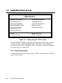
1
MIC-3355 6u-sized Pentium® processor-based CPU module for CompactPCI ® Copyright Notice This document is copyrighted, 1998. All rights are reserved. The original manufacturer reserves the right to make improvements to the products described in this manual at any time without notice. No part of this manual may be reproduced, copied, translated or transmitted in any form or by any means without the prior written permission of the original manufacturer. Information provided in this manual is intended to be accurate and reliable. However, the original manufacturer assumes no responsibility for its use, nor for any infringements upon the rights of third parties which may result from its use. Acknowledgements AMD is a trademark of Advanced Micro Devices, Inc. Award is a trademark of Award Software International, Inc. Cyrix is a trademark of Cyrix Corporation. IBM, PC/AT, PS/2 and VGA are trademarks of International Business Machines Corporation. Intel and Pentium are trademarks of Intel Corporation. Microsoft Windows® is a registered trademark of Microsoft Corp. PICMG™, CompactPCI™ and the PICMG™, CompactPCI™ logos are trademarks of the PCI Industrial Computers Manufacturers Group RTL is a trademark of Realtek Semi-Conductor Co., Ltd. SiS is a trademark of Silicon Integration Systems Corporation. All other product names or trademarks are properties of their respective owners. Part No. 2006335520 Printed in Taiwan MIC-3355 User's Manual 3rd Edition January 2000 Packing List Before installing your board, ensure that the following materials have been received: • 1 MIC-3355 all-in-one single board computer • 1CD-ROM disc including Ethernet utility programs, IDE utility programs and SVGA utility programs and drivers for Windows 3.1/ 95/NT and OS/2 • 1 hard disk drive (IDE) interface cable (44-pin) • 1 warranty certificate • This user's manual If any of these items are missing or damaged, contact your distributor or sales representative immediately. Preface and Table of Contents Contents Chapter 1: Hardware Configuration ............................................ 1 1.1 Introduction .................................................................... 2 1.2 Specifications .................................................................. 3 1.2.1 Standard SBC functions .............................................. 3 1.2.2 PCI-to-PCI Bridge ...................................................... 4 1.2.3 VGA interface ............................................................. 4 1.2.4 100Base-T Ethernet Interface ..................................... 4 1.2.5 Mechanical and environmental specifications ............. 5 1.3 Board Layout: Dimensions .......................................... 6 1.4 Jumpers and Connectors ............................................. 7 1.5 Board Layout: Jumper Locations ............................... 8 1.6 Board Layout: Connector Locations ........................ 10 1.7 Safety Precautions ....................................................... 11 1.8 Jumper Settings ........................................................... 12 1.9 Installing SDRAM (DIMMs) .................................... 15 Chapter 2: Connecting Peripherals ........................................... 17 2.1 IDE Device connector (CN10) and Floppy Drive connector (CN9) ............................... 19 2.2 VGA Display Connector (CN2) ..................................... 21 2.3 Parallel Port Connector (CN6) ...................................... 21 2.4 Keyboard and PS/2 Mouse Connector (CN1) .............. 21 2.5 Serial Ports (CN6: COM1 and COM2) ......................... 21 2.5.1 RS-232 connection (COM1-CN6) ............................. 22 2.5.2 RS-232/422/485 connection (COM2-CN6) ............... 22 2.6 Power Connectors (CN7 & CN8) .................................. 22 2.6.1 Main power connector +5 V, +12 V (CN7) ............... 22 2.6.2 CPU fan power supply connector (CN8) ................... 23 2.7 Ethernet Configuration (CN4) ....................................... 23 RJ-45A connector (CN4) .................................................... 23 Network boot ...................................................................... 23 2.8 USB Connector (CN5) ................................................ 23 MIC-3355 User's Manual 2.9 IR Interface (LED1) .................................................... 24 2.10 Card Installation ......................................................... 24 Chapter 3: VGA Display & Ethernet Software Configuration ... 27 3.1 Introduction .................................................................. 28 3.2 Utility and Drivers ....................................................... 28 3.3 VGA Display Setup and Configuration ..................... 30 3.3.1 VGA Display Setup and Configuration for DOS ....... 30 3.3.2 VGA Driver Setup for Autodesk ADI 4.2 (Protected Mode) ............................................ 32 3.3.3 VGA Display Setup and Configuration for Microsoft Windows NT 3.5x .................................. 32 3.3.4 VGA Display Setup and Configuration for Microsoft Windows NT 4.0 .................................... 34 3.3.5 VGA Display Setup and Configuration for Microsoft Windows 95 ............................................ 35 3.3.6 VGA Display Setup and Configuration for Microsoft Windows 3.x ............................................ 36 3.3.7 VGA Display Setup and Configuration for IBM OS/2 Ver. 2.1 .................................................... 39 3.3.8 VGA Display Setup and Configuration for IBM OS/2 Warp 3.0 (Double Byte Character) .......... 39 3.3.9 VGA Display Setup and Configuration for IBM OS/2 Warp 3.0 (Single Byte Character) ............ 40 3.4 Ethernet Software Configuration ............................... 41 Chapter 4: Award BIOS Setup ................................................... 43 4.1 AWARD BIOS Setup ................................................... 44 4.1.1 Entering setup ............................................................ 44 4.1.2 Standard CMOS setup .............................................. 45 4.1.3 BIOS features setup .................................................. 46 4.1.4 CHIPSET features setup .......................................... 50 4.1.5 Power management setup .........................................51 4.1.6 PCI configuration setup ............................................. 52 4.1.7 Load BIOS defaults................................................... 52 Preface and Table of Contents 4.1.8 Load setup defaults ................................................... 52 4.1.9 Integrated Peripherals ............................................... 53 4.1.10 Password setting ....................................................... 53 4.1.11 IDE HDD auto detection .......................................... 53 4.1.12 Save & exit setup .....................................................54 4.1.13 Exit without saving .................................................... 54 Appendix A: Programming the Watchdog Timer .................... 55 A.1 Programming the Watchdog Timer .......................... 56 Appendix B: Pin Assignments ................................................... 59 B.1 B.2 B.3 B.4 B.5 B.6 B.7 B.8 B.9 B.10 B.11 B.12 B.13 B.14 B.15 B.16 CRT Display Connector (CN2) ............................. 60 COM1 RS-232 Serial Port (CN6) ......................... 60 COM2 RS-232/422/485 Serial Port (CN6) .......... 61 Keyboard and Mouse Connnector (CN1) ........... 61 Main Power Connector (CN7) .............................. 62 IDE Hard Drive Connector (CN10) ..................... 63 USB Connector (CN5) ........................................... 64 CPU Fan Power Connector (CN8) ....................... 64 Ethernet RJ-45 Connector (CN4) ........................ 65 Floppy Drive Connector (CN9) ............................ 66 Parallel Port Connector (CN6) .............................. 67 System I/O Ports ..................................................... 68 DMA Channel Assignments ................................. 69 Interrupt Assignments ........................................... 70 1st MB Memory Map ............................................ 70 J3 Connector Pin Assignments ............................ 71 MIC-3355 User's Manual Figures Figure 1-1: Figure 1-2: Figure 1-3: Figure 1-4: Figure 2-1: Figure 2-2: Figure 4-1: Figure 4-2: Figure 4-3: Figure 4-4: Figure 4-5: Figure 4-6: Figure 4-7: MIC-3355 board layout: Dimensions ................................ 6 MIC-3355 board layout: Jumper locations ...................... 8 MIC-3355 board layout: Connector locations ............... 10 MIC-3355 board layout: Jumper settings ...................... 13 Installing the HDD ............................................................ 20 Installing the card into the chassis ............................... 25 Setup program initial screen ......................................... 44 CMOS setup screen ....................................................... 45 BIOS features setup screen .......................................... 46 CHIPSET features setup screen .................................... 50 Power management setup screen ............................... 51 PCI configuration screen ............................................... 52 Integrated peripherals ................................................... 53 Tables Table 1-1: Table 1-2: Table 1-3: Table 2-1: Table 2-3: Table B-1: Table B-2: Table B-3: Table B-4: Table B-5: Table B-6: Table B-7: Table B-8: Table B-9: Table B-10: Table B-11: Table B-12: Table B-13: Table B-14: Table B-15: Table B-16: Table B-17: MIC-3355 jumpers ............................................................ 7 MIC-3355 connectors ....................................................... 8 CPU clock ratio setting ................................................... 14 List of connectors .......................................................... 18 MIC-3355 serial port default settings ............................ 22 MIC-3355 CRT display connector .................................. 60 MIC-3355 COM1 RS-232 serial port ............................... 60 MIC-3355 COM2 RS-232/422/485 series port ............... 61 MIC-3355 keyboard connector ...................................... 61 MIC-3355 mouse connector .......................................... 62 MIC-3355 main power connector .................................. 62 MIC-3355 IDE hard drive connector ............................... 63 USB1/USB2 connector ................................................... 64 MIC-3355 CPU fan power connector ............................. 64 MIC-3355 Ethernet RJ-45 connector ............................. 65 MIC-3355 floppy drive connector ................................... 66 MIC-3355 parallel port connector .................................. 67 System I/O ports ............................................................. 68 DMA channel assignments ............................................ 69 Interrupt assignments ................................................... 70 1st MB memory map ...................................................... 70 J3 Connector Pin Assignments ..................................... 71 Preface and Table of Contents CHAPTER Hardware Configuration 1 This chapter gives background information on the MIC-3355. It then shows you how to configure the card to match your application and prepare it for installation into your chassis. Sections include: • Card specifications • Board layout: dimensions • Board layout: jumper locations • Board layout: connector locations • Safety precautions • Jumper settings • Installing SDRAM (DIMMs) 1.1 Introduction The MIC-3355 is a 6U-sized CompactPCI™, all-in-one single board Pentium® processor-based CPU card which complies with PICMG 2.0 R2.1 CompactPCI specifications. The MIC-3355 offers all the functions of an industrial computer on a single board CPU card. This card supports an Intel Pentium, Pentium MMX, AMD K5, AMD K6, Cyrix M1 or Cyrix M2 processor. The card accepts up to 256 MB SDRAM. It also supports on-board 512 KB PB-SRAM 2nd level cache. The MIC-3355 uses a single-chip solution, allowing on-board DRAM to be shared with the built-in VGA controller. In this configuration, the chipset always acts as the arbiter between memory bus masters. This system ensures efficient memory allocation while substantially reducing the overall system cost. On-board features include 512 KB 2nd level cache memory, 100/10 Mbps fast Ethernet interface, one RS-232 port, one RS-232/422/485 port, one multi-mode parallel (ECP/EPP/SPP) port, a floppy drive controller and a keyboard and PS/2 mouse interface. The built-in high speed PCI IDE controller supports both PIO and bus master modes. Two IDE channels are available through the J3 connector and one channel is available through the on-board connector. Up to two IDE devices can be connected to one channel, including large hard disks, CD-ROM drives, tape backup drives and other IDE devices. The MIC3355 also supports two USB ports and one fast infrared port. The MIC-3355 also features power management to minimize power consumption. It complies with the "Green Function" standard and supports three types of power saving features: Doze mode, Standby mode and Suspend mode. A watchdog timer can automatically reset the system or generate an interrupt should the system stop due to a program bug or EMI. 2 MIC-3355 User's Manual 1.2 Specifications 1.2.1 Standard SBC functions • CPU: Intel Pentium®, Pentium MMX, AMD K5, AMD K6, Cyrix M1, Cyrix M2, or IDT Win Chip C6 • BIOS: Award 256 KB (2 Mbit) memory; supports plug and play • Chipset: SiS5598 • L2 cache: On-board 512 KB synchronous (pipeline burst) SRAM • Green function: Features power management option via BIOS, activated by keyboard or mouse activity. Supports doze, standby and suspend modes. APM 1.1 compliant • RAM: Two 168-pin DIMM sockets. Supports SDRAM with memory capacity up to 256 MB • EIDE interface: Handles up to 4 IDE HDDs or other IDE devices via the J3 connector, or 2 IDE devices through the on-board connector. Supports PIO mode 4 and Ultra DMA mode • FDD interface: Supports up to two floppy disk drives through the J3 connector or on-board connector • Parallel port: Configured to LPT1, LPT2, LPT3 or disabled. Supports multi-mode parallel port (SPP/ECP/EPP) • Serial ports: Two 16C550 UARTs, one RS-232, one RS-232/422/485 interface • Watchdog timer: Can generate a system reset or IRQ 15. Software enabled/disabled. Time interval is from 1 to 63 seconds, jumperless with run-time setup • Keyboard/mouse connector: 6-pin mini-DIN connector on the front panel • USB interface: Two USB connectors with fuse protection. Complies with USB specification 1.0 • Infrared port: Fast IrDA. Transfer rate up to 4 Mbps. I/O port programmable to COM1 (3F8), COM2 (2F8), COM3 (3E8) or COM4 (2E8). Chapter 1 Hardware Configuration 3 1.2.2 PCI-to-PCI Bridge • Controller chip: Texas Instruments PCI2031 • Support up to six secondary bus masters. (Bus master cards can be installed in any slots except logic slot 8. Logic slot 8 accepts only slave card.) 1.2.3 VGA interface • Chipset: SiS5598 built-in VGA function • Architecture: Universal memory architecture • Display memory: Share system RAM 0.5 MB ~ 4 MB through BIOS setting (refer to section 4.1.4 for detail) • Display Resolution: • • • • • • 640 x 480 with 256/32K/64K/16M color display, NI 800 x 600 with 16/256/32K/64K/16M color display, NI 1024 x 768 with 16/256/32K/64K/16M color display, NI 1280 x 1024 with 16/256 color display, NI 1280 x 1024 with 32K/64K color display, interlaced only 1600 x 1200 with 256 color display, NI 1.2.4 100Base-T Ethernet Interface • Chipset: REALTEK RTL8139A. PCI bus 100/10 Mbps Ethernet controller • Built-in boot ROM 4 MIC-3355 User's Manual 1.2.5 Mechanical and environmental specifications • Board size: 233.35 x 160 mm (6u size) • Max. power requirements: +5 V (4.75 ~ 5.25 V) @ 5.5 A • Operating temperature: 0 ~ 60° C (32 ~ 140° F) • Storage temperature: -20° C ~ 70° C(-4° ~ 158° F) • Humidity (operating and storage): 5 ~ 95% (non-condensing) • Board weight: 0.65 kg (1.4 lb) • Operating altitude: 0 to 10,000 feet (3048 meters) • Storage/transit altitude: 0 to 40,000 feet (12,190 meters) • Shock: 20 G (operating); 50 G (storage/transit) • Vibration:1.5 G at 5-39 Hz, 100 - 200 Hz; 0.5 G 40 - 99 Hz (Y-axis) 1.5 G at 5-39 Hz, 0.5 G 40 - 200 Hz (X-axis) 1.5 G at 5-49 Hz, 0.75 G 50 - 200 Hz (Z-axis) Chapter 1 Hardware Configuration 5 1.3 Board Layout: Dimensions 233.35 mm 160 mm Figure 1-1: MIC-3355 board layout: Dimensions 6 MIC-3355 User's Manual 1.4 Jumpers and Connectors On-board connectors link it to external devices such as hard disk drives, a keyboard, or floppy drives. In addition, the board has jumpers for configuring your board for specific applications. The table below lists the function of each of the board's jumpers and connectors. Later sections in this chapter give instructions on setting jumpers and detailed information on each jumper setting. Chapter 2 gives instructions for connecting external devices to your card. Table 1-1: MIC-3355 jumpers Number Function JP1 CPU dual/single power setting JP2 CPU clock setting JP3 COM2 RS-232/422/485 selection JP4 COM2 RS-232/422/485 setting JP5 COM2 RS-232/422/485 setting JP6 CPU clock ratio setting JP7 Watchdog timer control setting JP9 Cyrix linear mode setting JP10 CPU core voltage setting JP11 clear CMOS Chapter 1 Hardware Configuration 7 Table 1-2: MIC-3355 connectors Number Function CN1 Keyboard and PS/2 mouse CN2 VGA connector CN3 Reset switch CN4 10/100 Mbps LAN connector CN5 USB connector CN6 COM1, COM2, parallel port CN7 Main power connector CN8 CPU fan power connector CN9 Floppy disk connector CN10 IDE connector LED1 IR LED2 Power, HDD activity LED LED3 LAN LED Please refer to Appendix B for pin assignments. 8 MIC-3355 User's Manual 1.5 Board Layout: Jumper Locations JP9: Cyrix linear mode setting JP10: CPU core voltage setting JP6: CPU clock ratio setting JP2: CPU clock setting JP1: Dual/Single power setting JP7: watchdog timer control JP4 & JP5: RS-232 and RS-422/485 signal selector JP11: clear CMOS JP3: RS-232/422/ 485 mode selector Figure 1-2: MIC-3355 board layout: Jumper locations Chapter 1 Hardware Configuration 9 1.6 Board Layout: Connector Locations Figure 1-3: MIC-3355 board layout: Connector locations 10 MIC-3355 User's Manual 1.7 Safety Precautions Follow these simple precautions to protect yourself from harm and your PC from damage. 1. To avoid electric shock, always disconnect the power from your PC chassis before you work on it. Don't touch any components on the CPU card or other cards while the PC is on. 2. Disconnect power before making any configuration changes. The sudden rush of power as you connect a jumper or install a card may damage sensitive electronic components. 3. Always ground yourself to remove any static charge before you touch your CPU card. Be particularly careful not to touch the chip connectors. Modern integrated electronic devices, especially CPUs and memory chips, are extremely sensitive to static electric discharges and fields. Keep the card in its antistatic packaging when it is not installed in the PC, and place it on a static dissipative mat when you are working with it. Wear a grounding wrist strap for continuous protection. Chapter 1 Hardware Configuration 11 1.8 Jumper Settings This section tells how to set the jumpers to configure your card. It gives the card default configuration and your options for each jumper. After you set the jumpers and install the card, you will also need to run the BIOS Setup program (discussed in Chapter 4) to configure the serial port addresses, floppy/hard disk drive types and system operating parameters. Connections, such as hard disk cables, appear in Chapter 2. For the locations of each jumper, see the board layout diagram depicted earlier in this chapter. You configure your card to match the needs of your application by setting jumpers. A jumper is the simplest kind of electric switch. It consists of two metal pins and a small metal cap (often protected by a plastic cover) that slides over the pins to connect them. To "close" a jumper you connect the pins with the cap. To "open" a jumper you remove the cap. Sometimes a jumper will have three pins, labeled 1, 2 and 3. In this case you connect either pins 1 and 2 or 2 and 3. 1 Open Closed 2 3 Closed 2-3 You may find a pair of needle-nose pliers useful for setting the jumpers. If you have any doubts about the best hardware configuration for your application, contact your local distributor or sales representative before you make any changes. 12 MIC-3355 User's Manual Figure 1-4: MIC-3355 board layout: Jumper settings Chapter 1 Hardware Configuration 13 8 6 4 2 2. 1 : P54C 2. AMD K6 1-2 3-4 5-6 x x x o o x o x x x o x x x o o o o o x o x o o : 75 MHz : 60 MHz : 66 MHz 2.1 3.1 4.1 ratio 3.5 2.5 2 3 5.5 4.5 5 4 JP6: CPU clock ratio setting x: open o: close 1. Intel CPU ratio 1-2 3-4 5-6 P54C P55C x x x 1.5 3.5 o o x 2.5 2.5 o x x 2 2 x o x 3 3 J2: CPU clock setting 1.1 : 55 MHz 1 6 4 2 5 3 1 JP9 Cyrix CPU 1. : normal 2. : linear mode JP1: P54C/P55C Power setting 1. : P55C (MMX) 1 1 JP10: CPU core voltage x: open o: close 1-2 3-4 5-6 7-8 Vcore x x x x 2.1 o x x x 2.2 x o x x 2.3 o o x x 2.4 x x o x 2.5 o x o x 2.6 x o o x 2.7 o o o x 2.8 x x x o 2.9 o x x o 3.0 x o x o 3.1 o o x o 3.2 x x o o 3.3 o x o o 3.4 x o o o 3.5 o o o o 3.6 7 5 3 1 2. : Normal 3 1 5 3. 1 3 5 2. 1 3 5 : RS-232 : RS-422 : RS-485 JP3: COM2 MODE 1. : reset system JP11: CMOS 1. : clear CMOS (when power is on) 2. 3 2 1 JP7: Watchdog control 1. 3 2 1 : IRQ15 1 1 3 1 3 1 5 5 3 3 2. 5 5 : RS-232 : RS-422/485 JP4,JP5: COM2 Signal Selector 1. CPU Clock Ratio Setting Table 1-3: CPU clock ratio setting CPU mode CPU Bus Clock JP6 JP2 clock clock Ratio 1-2 3-4 5-6 1-2 3-4 Pentium 233MHz 233 66 3.5 x x x x x Pentium 200MHz 200 66 3.0 x o x x x Pentium 166MHz 166 66 2.5 o o x x x Pentium 150MHz 150 60 2.5 o o x o x Pentium 133MHz 133 66 2.0 o x x x x Pentium 120MHz 120 60 2.0 o x x o x Pentium 100MHz 100 66 1.5 x x x x x Pentium 90MHz 90 60 1.5 x x x o x o Pentium 75MHz 75 50 1.5 x x x o AMD K6-300 300 66 4.5 o o o x x AMD K6-266 266 66 4.0 o x o x x AMD K6-233 233 66 3.5 x x x x x AMD K6-200 200 66 3.0 x o x x x AMD K6-166 166 66 2.5 o o x x x Cyrix 6x86MX-PR166GP 133 66 2.0 o x x x x Cyrix 6x86MX-PR166GP 150 60 2.5 o o x o x Cyrix 6x86MX-PR200GP 166 66 2.5 o o x x x *Cyrix 6x86MX-PR200GP 150 75 2.0 o x x x o *Cyrix 6x86MX-PR233GP 187.5 75 2.5 o o x x o *Cyrix MII-300GP 225 75 3.0 x o x x o Cyrix MII-300GP 233 66 3.5 x x x x x IDT WinChip C6-180 180 60 3.0 x o x o x IDT WinChip C6-200 200 66 3.0 x o x x x *IDT WinChip C6-225 225 75 3.0 x o x x o IDT WinChip C6-240 240 60 4.0 o x o o x x: open o: closed *: Bus clock of 75 MHz is not recommended to use. 14 MIC-3355 User's Manual JP9 Cyrix CPU This jumper is for Cyrix CPUs only. Close it only when using Cyrix brand CPUs. JP11 Clear CMOS This jumper is used to erase CMOS data and reset system BIOS information. The procedure for clearing CMOS appears below. 1. Turn off the system. 2. Short JP11 3. Turn on the system. The CMOS is now cleared. 4. Turn off the system. Open JP11. 5. Turn on the system. The BIOS is reset to its default setting. 1.9 Installing SDRAM (DIMMs) The MIC-3355 provides two 168-pin DIMM sockets. Each socket accepts 16, 32, 64 or 128 MB SDRAM with access time ≤ 60 ns. The MIC-3355 supports a single SDRAM which has to be installed in Bank 0 for on-board VGA. NOTE: The modules can only fit into a socket one way. Their gold pins must point down into the DIMM socket. The procedure for installing DIMMs appears below. Please follow these steps carefully. 1. Ensure that all power supplies to the system are switched Off. 2. Install the DIMM module. Install the DIMM so that its gold pins point down into the DIMM socket. 3. Slip the DIMM into the socket and carefully fit the bottom of the card against the connectors. Chapter 1 Hardware Configuration 15 4. Gently push the DIMM into a perpendicular position until the clips on the ends of the DIMM sockets snap into place. 5. Check to ensure that the DIMM is correctly seated and all connector contacts touch. The DIMM should not move around in its socket. 16 MIC-3355 User's Manual CHAPTER Connecting Peripherals 2 This chapter tells how to connect peripherals to the MIC-3355. You can access most of the connectors from the front panel. The following table lists the connectors on the MIC-3355. Table 2-1: List of connectors Number Function J1 Compact PCI bus (32-bit) J2 Compact PCI bus (64-bit) J3 IDE and FDD interface CN1 Keyboard and PS/2 mouse CN2 VGA connector CN3 Reset switch CN4 100/10 Mbps LAN connector CN5 USB connector CN6 COM1, COM2, parallel port CN7 Main power connector CN8 CPU fan connector CN9 Floppy disk connector CN10 IDE connector (primary) LED1 Infrared interface LED2 Power, HDD activity LED LED3 LAN LED The following sections tell how to make each connection. In most cases, you will simply need to connect a standard cable. All of the connector pin assignments are shown in Appendix B. Warning! Always completely disconnect the power cord from your chassis whenever you are working on it. Do not make connections while the power is on. Sensitive electronic components can be damaged by a sudden rush of power. 18 MIC-3355 User's Manual Caution! Always ground yourself to remove any static charge before touching the CPU card. Modern electronic devices are very sensitive to static electric charges. Use a grounding wrist strap at all times. Place all electronic components on a static-dissipative surface or in a static-shielded bag when they are not in the chassis. 2.1 IDE Device connector (CN10) and Floppy Drive connector (CN9) The MIC-3355 provides two IDE (Integrated Device Electronics) channels and one floppy drive interface through the CompactPCI J3 connector. These connect to two IDE and one floppy drive connectors on Advantech's 6U-sized backplane. The primary IDE channel is also available through the on-board 44-pin connector (CN10), which accepts a 2.5" hard drive by using the hard drive bracket, or an IDE flash disk module (i.e., Advantech's PCD-1230). Users can attach two IDE devices to each IDE channel, either to the backplane or to the on-board connector. If two drives are installed in one channel, remember to set one as the master and the other one as the slave. You may do this by setting the jumpers on the drives. Refer to the documentation that came with your drive for more information. A jumper diagram usually appears on the top side of a hard disk drive. Users can attach up to two floppy disk drives to the floppy connector on the backplane. The MIC-3355 supports any combination of 5.25" (360 KB/1.2 MB) and/or 3.5" (720 KB/1.44/2.88 MB) drives. The on-board connector (CN9) can also be used to connect to a 3.5" floppy drive by using a 26-pin FPC cable. However, due to the limited space, there is no access to the floppy drive on the front panel. We do not recommend the use of this connector. Chapter 2 Connecting Peripherals 19 Warning: Plug the other end of the cable into the drive with pin 1 on the cable corresponding to pin 1 on the drive. Improper connection will damage the drive. Note: We don't recommend connection to following IDE HDD models of Seagate: ST 31276A, ST 31720A, ST 32531A, ST 33240A or ST 34340A Figure 2-1: Installing the HDD 20 MIC-3355 User's Manual 2.2 VGA Display Connector (CN2) The MIC-3355 provides a VGA controller for a high resolution VGA interface. The MIC-3355's CN2 is a DB-15 connector for VGA monitor input. Pin assignments for the CRT display are detailed in Appendix B. Share memory architecture supports 0.5 MB, 1 MB, 1.5 MB, 2 MB, 2.5 MB, 3 MB, 3.5 MB and 4 MB system memory. The memory is configured in the system BIOS setup. 2.3 Parallel Port Connector (CN6) The parallel port is normally used to connect the CPU card to a printer. The MIC-3355 includes an on-board parallel port, accessed through a DB 25-pin connector, CN6 on the front panel. The parallel port is designated as LPT1 and can be disabled or changed to LPT2 or LPT3 in the system BIOS setup. 2.4 Keyboard and PS/2 Mouse Connector (CN1) The MIC-3355 provides two connectors for connection of keyboard and PS/2 mouse on the front panel. Since these two connectors are identical, please be careful to plug in keyboard or mouse into the correct connector. 2.5 Serial Ports (CN6: COM1 and COM2) The MIC-3355 offers two serial ports: COM1 in RS-232, COM2 in RS-232/422/485. These ports let you connect to serial devices (a mouse, printers, etc.) or a communication network. You can select the address for each port ( For example, 3F8H [COM1], 2F8H [COM2]) or disable it, using the BIOS Advanced Setup program, covered in Chapter 4. Chapter 2 Connecting Peripherals 21 2.5.1 RS-232 connection (COM1-CN6) Different devices implement the RS-232 standard in different ways. If you are having problems with a serial device, be sure to check the pin assignments for the connector. 2.5.2 RS-232/422/485 connection (COM2-CN6) COM2 is an RS-232/422/485 serial port. The specific port type is determined by jumper settings, as detailed in Chapter 1. The IRQ and address range for both ports are fixed. However, if you wish to disable the port or change these parameters later, you can do this in the system BIOS setup. The table below shows the settings for the MIC-3355 board's ports: Table 2-3: MIC-3355 serial port default settings Port Address Default COM1 3F8, 2F8, 3E8, 2E8 3F8/IRQ4 COM2 3F8, 2F8, 3E8, 2E8 2F8/IRQ3 2.6 Power Connectors (CN7 & CN8) 2.6.1 Main power connector +5 V, +12 V (CN7) The on-board power connector allows users to operate MIC-3355 with external power supply without plugging into a chassis. The CN7 provides power input connection to +5 V and +12V. 22 MIC-3355 User's Manual 2.6.2 CPU fan power supply connector (CN8) This connector provides power supply to the optional CPU cooling fan. This connector is only available when +5 V and +12 V power is supplied to the board. Warning! Before making the connection, make sure the voltage is absolutely correct and matched with the correct connector. 2.7 Ethernet Configuration (CN4) The MIC-3355 is equipped with a high performance 32-bit PCI-bus Fast Ethernet interface which is fully compliant with IEEE 802.3u 100/10Base-T specifications. It is supported by all major network operating systems and is 100% Novell NE-2000 compatible. The medium type can be configured via the RSET8139.EXE program included on the utility CD-ROM disc. (See Chapter 3 for detailed information.) RJ-45A connector (CN4) 100/10BASE-T connects to the MIC-3355 via an adapter cable to the RJ-45 standard jack. Network boot The Network Boot feature is built into the BIOS. It can be enabled/ disabled in the chipset setup of the CMOS configuration. Refer to "BIOS Setting" in Chapter 4 for more information. 2.8 USB Connector (CN5) The MIC-3355 board provides two USB (Universal Serial Bus) interfaces, which give complete plug and play, hot attach/detach for up to 127 external devices. The USB interfaces comply with USB specification rev. 1.0 and are fuse protected. The USB interfaces can be disabled in the system BIOS setup. Chapter 2 Connecting Peripherals 23 2.9 IR Interface (LED1) The IR interface supports the wireless infrared transmitting and receiving module. You must configure the setting through BIOS setup. 2.10 Card Installation The CompactPCI connectors are firm and rigid, and require careful handling while plugging and unplugging. Improper installation of a card can easily damage the backplane of the chassis. The insert/eject handles of MIC-3355 help you to install and remove the card easily and safely. Follow the procedure below to install the MIC-3355 into a chassis: To install a card: 1. Hold the MIC-3355 vertically. Be sure that the card is pointing in the correct direction. The components of the card should be pointing to the right-hand side. 2. Holding both handles, pull out the red portion in the middle of the handle to unlock it. Caution: Keep your fingers away from the hinge to prevent your fingers from getting pinched. 3. Insert the card into the chassis by sliding the upper and lower edges of the card into the card guide. 4. Push the card into the slot gently by sliding the card along the card guide until the handles meet the rectangular holes of the cross rails. Note: If the card is correctly positioned and has been slid all the way into the chassis, the handles should match the rectangular holes. If not, remove the card from the card guide and repeat step 3 again. Do not try to install a card by forcing it into the chassis. 5. Pull the upper handle down and lift the lower handle up to push the card into place. 24 MIC-3355 User's Manual 6. Secure the card by pushing in the red handle to lock it into place. To remove a card: 1. Unscrew the four screws on the front panel. Pull out the red part to unlock the handles. 2. Lift the upper handle up and press the lower handle down to release the card from the backplane. 3. Slide the card out. Keep your fingers away from this area. Figure 2-2: Installing the card into the chassis Chapter 2 Connecting Peripherals 25 26 MIC-3355 User's Manual CHAPTER 3 VGA Display & Ethernet Software Configuration This chapter details the software configuration information. It shows you how to configure the board to match your application requirements. The AWARD System BIOS is covered in Chapter 4. Sections include: • VGA display configuration • Ethernet interface configuration 3.1 Introduction The MIC-3355 uses the SiS5598 chipset. This chipset includes a highperformance VGA display controller, which uses system SDRAM as display memory. The shared memory size can easily be adjusted from 0.5 MB to 4 MB by setting BIOS, which is covered in Chapter 4. The larger memory size allows high display resolution and more display color. 3.2 Utility and Drivers The MIC-3355 is supplied with a software utility CD-ROM that holds the necessary files for setting up the VGA display and Ethernet under the directory \MIC3000\SiS5598 and \MIC3000\RTL8139A. The following lists the contents and pathnames of this CD-ROM: • MIC3000\SiS5598\README.TXT: ASCII text file. • MIC3000\SiS5598\RELEASE.TXT: Text file of driver release note • MIC3000\SiS5598\IDE <DIR>: SiS IDE drivers and Readme files for SiS chipset 5513, 5571, 5581, 5582, 5597, 5598, 559 and 5592 • MIC3000\SiS5598\MM <DIR>: SISTAG (disk tag file for Windows NT 3.5x) • MIC3000\SiS5598\MM <DIR>: RELEASE.TXT (Text file of driver release note) • MIC3000\SiS5598\MM\BIOS <DIR>: contains SiS SVGA BIOS binary file. It is not a driver file but for your reference only. • MIC3000\SiS5598\MM\DOS <DIR>: Including the following files and sub-directories: • INSTDRV.EXE: Unpack & copy program of ADI 4.2 28 MIC-3355 User's Manual • SVGAUTIL.EXE: SiS5598 SVGA Utility Program • MIC3000\SiS5598\MM\DOS\ADI42 <DIR>: Contains AutoCAD, AutoShade, 3D Studio driver files • MIC3000\SiS5598\ MM\DOS\ET <DIR>: Contains ETen Chinese system display driver (ETDSPDRV.COM) v. 119B01 to support SiS SVGA. You may update this driver to your ETen Chinese system if you have the old version or you may ignore it if you have the newer version. • MIC3000\SiS5598\MM\OS2 <DIR>: Contains IBM OS/2 Ver. 2.1, IBM OS/2 Warp 3.0 (double-byte) and IBM OS/2 Warp 3.0 (single byte) driver files. Including the following sub-directories: • MIC3000\SiS5598\OS2\SBCS.21 <DIR>: SISINST.CMD: SiS 5597/5598 VGA OS/2 2.1 setup program • MIC3000\SiS5598\OS2\DBCS.30 <DIR>: SETUP.CMD: SiS 5597/5598 SVGA OS/2 3.0 setup program, contains IBM OS/2 WARP 3.0 (double-byte: Chinese, Japanese, Korean, etc.) driver files. • MIC3000\SiS5598\OS2\SBCS.30 <DIR>: SISINST.CMD: SiS 5597/5598 VGA OS/2 3.0 Setup Program, contains IBM OS/2 WARP 3.0 (single-byte) driver files. • MIC3000\SiS5598\MM\WIN31 <DIR>: Contains Windows 3.X driver, setup program, SiS MMPlayer and utilities. • MIC3000\SiS5598\MM\WIN95 <DIR>: Contains Windows 95 driver, setup program, SiS MMPlayer, Direct Draw driver and utilities. Chapter 3 VGA Display & Ethernet Software Configuration 29 • MIC3000\SiS5598\MM\WINNT <DIR>: Contains Windows 3.5x, 4.0 driver files and contains the following sub-directories: • MIC3000\SiS5598\WINNT\WINNT35 <DIR>: Contains Windows NT 3.5x driver files OEMSETUP.INF: SiS SVGA setup information file (NT 3.5x) • MIC3000\SiS5598\WINNT\WINNT40 <DIR>: Contains Windows NT 4.0 driver files SISV5597.INF: SiS SVGA setup information file (NT 4.0) 3.3 VGA Display Setup and Configuration 3.3.1 VGA Display Setup and Configuration for DOS 3.3.1.1. General Description SVGAUTL.EXE is one of the utilities for VGA controller SiS5598. It supports three functions: 1. Video mode setting 2. Frame rate setting 3. Power saving setting Since SiS5598 supports many enhanced text mode and graphic modes, you can use SVGAUTL.EXE to select the desired video mode. For 640 x 480, 800 x 600, 1024 x 768 and 1280 x 1024 resolutions, SiS5598 SVGA supports multiple frame rates. If your monitor could synchronize with these frame rates, you can use SVGAUTL.EXE to take advantage of your monitor's features. SiS 5597/5598 also supports VESA DPMS power saving modes. SVGAUTL.EXE can help you make the settings. 3.3.1.2. How to Use SVGAUTL.EXE, 1. Type "SVGAUTL" in the directory where it resides. For example: D:\MIC3000\SiS5598\DOS\SVGAUTL <Enter> (assume the CD-ROM drive letter is "D:\") 30 MIC-3355 User's Manual 2. The Main Menu appears and directs you to configure SiS5598. 3. When you complete configuration, you may save your preferences to the AUTOEXEC.BAT file and use it as your power-on (or hardware reset) default environment. 3.3.1.3. Parameters Explanation The meaning of parameters used by SVGAUTL.EXE are explained below: Syntax: >SVGAUTL [/D:mode_no] [/F0:n0] [/F1:n1] [/F2:n2] [/F3:n3] [/PA:ta] [/PB:tb] where /D: Set the video mode to be mode_no (hex) For example: Set 1024 x 768, 256-color graphic mode: >SVGAUTL /D:38 <Enter> /F0: For 640 x 480, set frame rate to be n0 Hz. Three available frame rates are 60, 72 and 75 Hz. For example: Set 640 x 480 graphic mode with 60 Hz frame rate >SVGAUTL /F0:60 <Enter> /F1: For 800 x 600, set frame rate to be n1 Hz. Four available frame rates are 56, 60, 72 and 75 Hz. For example: Set 800 x 600 graphic mode with 72 Hz frame rate: >SVGAUTL /F1:72 <Enter> /F2: For 1024 x 768, set frame rate to be n2 Hz. Four available frame rates are 87 (interlaced), 60, 70, and 75 Hz. For example: Set 1024 x 768 graphic mode with 60 Hz frame rate: >SVGAUTL /F2:60 <Enter> /F3: For 1280 x 1024, set frame rate to be n3 Hz. Chapter 3 VGA Display & Ethernet Software Configuration 31 Two available frame rates are 87 (interlaced) and 60 Hz. For example: Set 1280 x 1024 graphic mode with 60 Hz frame rate: >SVGAUTL /F3:60 <Enter> /PA: Set standby timer to be ta minutes. (0 < ta < 15 min.) For example: Set Standby Timer to be 5 minutes: >SVGAUTL /PA:5 <Enter> /PB: Set suspend timer to be tb minutes. (0 < tb < 15 min.) For example: Set suspend timer to be 5 minutes: >SVGAUTL /PB:5 <Enter> Note: 1. Suspend time would be "ta + tb". (i.e. standby time + suspend time) 2. The timers will not be very accurate and approximate the time that you set 3.3.2 VGA Driver Setup for Autodesk ADI 4.2 (Protected Mode) Concerning how to setup VGA for AutoCAD R11, AutoCAD R12, AutoShade R2.0 and 3D Studio Version 3.0., please refer to MIC3000\SiS5598\README.TXT on the accompanying CD-ROM disc. 3.3.3 VGA Display Setup and Configuration for Microsoft Windows NT 3.5x 3.3.3.1 Driver Installation: a. Select Control Panel from Main group. b.Select Display icon. c. Select Change Display Type from Display Settings. d. Select Change from Display Type. 32 MIC-3355 User's Manual e. Select Other from Select Device. f. Place the CD-ROM into CD-ROM Drive. g. When the "Install from Disk" dialog box appears, type "D:\MIC3000\SiS5598\MM\WINNT\WINNT35" and click "OK". h. Select Install and click "Yes" when the "Installing Driver" dialog box appears. i. Select New when the "Windows NT Setup" dialog box appears. Click "Continue". A message will appear stating that the drivers were successfully installed. Click "OK". You must now restart Windows NT 3.51. 3.3.3.2 Selecting resolution and color depth: a. Select Control Panel from the Main group. b. Select Display icon. c. Select Color Palette to change between 16 colors, 256 colors, 32768 colors, 65536 colors and 16777216 colors. d. To select desktop resolution size, go to the Desktop area and use the slide bar to change resolution from 640 x 480, 800 x 600, 1024 x 768, and 1280 x 1024. e. Select Test to test the resolution. f. If the display test screen was good then select "Yes" when the "Testing Mode" dialog box appears. If the display test screen was bad then select "No". Windows NT will give you an error message. g. If the display test screen was good and you select "Yes", Windows NT 3.5x will prompt you to restart Windows NT 3.5x. 3.3.4 VGA Display Setup and Configuration for Microsoft Windows NT 4.0 Chapter 3 VGA Display & Ethernet Software Configuration 33 3.3.4.1 Driver Installation: a. Click the "Start" menu and select Control Panel from the Settings group. b. Select the Display icon. c. Select Settings of Display Properties. d. Select Display Type. e. Select Change from the Adapter Type area. f. Select Have Disk in the Change Display screen. g. Place the CD-ROM disc into the CD-ROM drive. h. When the "Install from Disk" dialog box appears, type "D:\MIC3000\SiS5598\ MM\WINNT\WINNT40" and click "OK". i. When the "Change Display" dialog box appears, click "OK". j. When the "Third-party Drivers" dialog box appears, click "Yes". A message will appear stating that the drivers were successfully installed. Click "OK". You must now restart Windows NT 4.0. 3.3.4.2 Selecting resolution and color depth a. Click the "Start" menu and select Control Panel from the Settings group. b. Select Display icon. c. Select Settings. d. Select Color Palette to change between 16 colors, 256 colors, 32768 colors, 65536 colors and 16777216 colors. e. To select desktop resolution size, go to the Desktop area and use the slide bar to change resolution from 640 x 480, 800 x 600, 1024 x 768 to 1280 x 1024. f. Select Test to test the resolution. If the display test screen was good then select "Yes" when the "Testing Mode" dialog box appears. If the display test screen was bad then select "No". Windows NT will give you an error message. g. Click "OK". If the display test screen was good and you select "Yes", Windows NT 4.0 will change the mode without restarting Windows NT 4.0. 34 MIC-3355 User's Manual 3.3.5 VGA Display Setup and Configuration for Microsoft Windows 95 3.3.5.1 Driver Installation a. Click "Start" menu and select Control Panel from Settings group. b. Select "Display" icon. c. Select "Settings" index in the display properties sheet. d. Select "Change Display Type" button. e. Select "Change..." button in "Adapter Type" group. f. Select "Have Disk" button. g. Place the CD-ROM disc into CD-ROM drive. h. When the "Install from Disk" dialog box appears, type "D:\MIC3000\SiS5598\ MM\WINNT\WIN95" and click "OK". i. When the "Change Display" dialog box appears, click "Close". j. Select the "Close" or "Apply" button from the display properties sheet. k. A message will appear stating that you must restart Windows 95. Select "yes" to restart. l. After restarting, Windows 95 will run on 640 x 480 at 256 colors, 75Hz NI. 3.3.5.2 Selecting resolution, color depth, and refresh rate a. Click "Start" menu and select Control Panel from Settings group. b. Select Display icon. c. Select Settings. d. Select Color Palette to change between 16-color, 256-color, Hicolor, and True-color. e. To select desktop resolution size, go to the Desktop area and use the slide bar to change resolution from 640 x 480, 800 x 600, 1024 x 768 and 1280 x 1024. f. Select Refresh rate list box to change the screen refresh rate. Chapter 3 VGA Display & Ethernet Software Configuration 35 g. Click "OK" or "Apply". 3.3.5.2 Install the Utility for Windows 95 a. Place the CD-ROM disc into the CD-ROM drive. b. Click "Start" menu and select "Run..." menu item. c. In "Run" dialog, type: "D:\MIC3000\SiS5598\MM\WIN95\SETUP.EXE" d. The Setup procedure will create a "SiS Multimedia Vx.xx" program group, including 3 items: • Multimedia Manager • SiS MMPlayer • Center Screen e. A Setup Successful dialog will appear when setup completes. You are given the option of restarting your computer and finalizing the changes. 3.3.6 VGA Display Setup and Configuration for Microsoft Windows 3.x 3.3.6.1 Display Driver and Utility Installation a. Click "File" menu and select "Run..." menu item. b. In "Run" dialog, type: D:\MIC3000\SiS5598\MM\WIN31\SETUP.EXE c. Follow the setup program's on-screen instructions. d. Setup procedure will create a "SiS Multimedia Vx.xx" program group, including 5 items: • Multimedia Manager • SiS MMPlayer • SVGA Setup • Center Screen • Uninstall 36 MIC-3355 User's Manual e. A Setup Successful dialog will appear when setup completes. You are given the option of restarting your computer and finalizing the changes. 3.3.6.2. Graphics Setup a. In the "SiS Multimedia Vx.xx" program group, choose "SVGA Setup" icon to enter "SiS VGA Configuration System" screen. b. In "SiS VGA Configuration System" screen, choose which options you would like to use. c. After completing your selections, choose "OK" to make all your selections effective. d. Choose "Restart Windows" to re-boot Windows using the new settings. Or, choose "Continue" to finalize the changes later. 3.3.6.3. Power Saving Setup in Windows a. In the "SiS VGA Configuration System" screen, choose "power saver" item to enter "Power Saver" screen. b. In the "Power Saver" Screen, choose which options you would like to use. c. After completing the selections, choose "OK" to make all your selections effective. d. After completing setup, the power_saver should take effect after the time interval has elapsed. 3.3.6.4. Zoom_Key Setup In the "SiS VGA Configuration System" screen, choose "zooming" item to define "hot keys" for enlarging or making the screen smaller without entering the setup program. The operation principles of zoom-in and zoom-out are as follows: 1.The resolution change sequence for zoom-in is: 1024 x 768 ——→ 800 x 600 ——→ 640 x 480 2. The resolution change sequence for zoom-out is: 640 x 480 ——→ 800 x 600 ——→ 1024 x 768 Note: You cannot zoom-out to a resolution larger than you have previously configured. Chapter 3 VGA Display & Ethernet Software Configuration 37 To use this feature,follow this procedure: a. In the "SiS VGA Configuration System" screen, choose "zooming" item to enter the "Zooming Hotkey" screen. b. In the "Zooming Hotkey" Screen, choose which "hot-key" you would like to use and enable it. c. After completing the selections, choose "OK" to make all your selections effective. d. After completing the setup, you may use your own defined hot key to zoom-in or zoom-out. Note: The power saver's timer settings would be effective even after exiting Windows back to DOS. 3.3.6.5 MPEG1 Video Operations SiS 5597/5598 supports DCI drivers for software MPEG playback and other media player programs which can take advantage of DCI. The SiS 5597/5598 DCI driver is automatically loaded during the "Windows Driver Unpack & Copy" process. Therefore it should be transparent to the end-user and any media players can take advantage of it. To make software MPEG playback better than what your original software MPEG player supplier provided, SiS provide an MMPlayer application program to provide a VCP-like (Video Cassette Player) interface. To take advantage of the SiS MMPlayer, you must first install "SW MPEG Player". SiS provides an interface but not a software MPEG player. If the software MPEG player (Xing or Mediamatics) does not exist, the SiS MMPlayer will not work. To use the SiS MMPlayer, choose the "SiS MMPlayer" icon in the "SiS Multimedia Vx.xx" program group and the SiS MMPlayer VCPlike icon will appear. You can then enjoy the software MPEG playback. 38 MIC-3355 User's Manual 3.3.7 VGA Display Setup and Configuration for IBM OS/2 Ver. 2.1 3.3.7.1 OS2 V2.1 Display Driver Installation a. Before installing SiS OS/2 V2.1 display driver, start up OS/2 system in standard VGA mode. b. Select "Command Prompt" folder. c. Select "OS/2 window" or "OS/2 full screen" icon. d. Place the CD-ROM disc into the CD-ROM drive. e. Change the directory to D:\MIC3000\SiS5598\MM\OS2\SBCS.21. f. Type SISINST then press "Enter". g. When the "Select Screen Parameters for SiS SVGA" dialog appears, select the resolution, color depth and frame rate you would like, then click "OK" h. The installation program will create a "SiS Setup" icon on the desktop. i. Shut down and re-boot OS/2 V2.1. 3.3.8 VGA Display Setup and Configuration for IBM OS/2 Warp 3.0 (Double Byte Character) 3.3.8.1 OS/2 Warp Display Driver Installation (For DBCS version) a. Before installing SiS OS/2 Warp display driver, start up OS/2 system in standard VGA mode. b. Select "Command Prompt" folder. c. Select "OS/2 window" or "OS/2 full screen" icon. d. Place the CD-ROM disc into the CD-ROM drive. e. Change the directory to D:\MIC3000\SiS5598\MM\OS2\DBCS.30. f. Type SETUP and then press "Enter". g. Setup procedure will create a "SiS Install" icon on the desktop. h. Shutdown and reboot the OS/2 Warp system. Chapter 3 VGA Display & Ethernet Software Configuration 39 i. When the system reboots, double-click the "SiS Install" icon. It will perform the further installation. j. When the "Select Screen Parameters for SiS SVGA" dialog appears, select the resolution, color depth and frame rate you would like, then click "OK" k. The installation program will create a "SiS Setup" icon on the desktop. l. Shutdown and re-boot OS/2 Warp. 3.3.9 VGA Display Setup and Configuration for IBM OS/2 Warp 3.0 (Single Byte Character) 3.3.9.1 OS2 Warp Display Driver Installation (For SBCS version) a. Before installing the SiS OS/2 Warp display driver, start up OS/ 2 system in standard VGA mode. b. Select "Command Prompts" folder. c. Select "OS/2 window" or "OS/2 full screen" icon. d. Place the CD-ROM disc into the CD-ROM drive. e. Change directory to D:\MIC3000\SiS5598\MM\OS2\SBCS.30 f. Type SISINST and then press "Enter". g. When the "Select Screen Parameters for SiS SVGA" dialog appears, select the resolution, color depth and frame rate you would like and then click "OK". h. The installation program will create a "SiS Setup" icon on the desktop. i. Shutdown and re-boot OS/2 Warp. 40 MIC-3355 User's Manual 3.4 Ethernet Software Configuration The MIC-3355's on-board Ethernet interface supports all major network operating systems. To configure the medium type, to view the current configuration, or to run diagnostics: 1. Power-on the MIC-3355. Ensure that the utility CD-ROM disc is located in the CD-ROM drive. 2. At the prompt, type \MIC3000\RTL8139A\RSET8139.EXE and press <Enter>. The Ethernet configuration program will then be displayed. 3. This simple screen shows all the available options for the Ethernet interface. Just highlight the option you want to change by using the Up and Down keys. To change a selected item, press <Enter> and a screen will appear with the available options. Highlight your option and press <Enter>. Each highlighted option has a helpful message guide displayed at the bottom of the screen for additional information. 4. After you have made your selections and are certain it is the configuration that you want, press ESC. A prompt will appear asking if you want to save the configuration. Press Y if you want to save. The Ethernet Setup Menu also offers three very useful diagnostic functions: 1. Run EEPROM test. 2. Run Diagnostics on Board. 3. Run Diagnostics on Network. Each option has its own display screen which shows the format and result of any diagnostic tests undertaken. Chapter 3 VGA Display & Ethernet Software Configuration 41 42 MIC-3355 User's Manual CHAPTER 4 Award BIOS Setup This chapter describes how to set the card’s BIOS configuration data. 4.1 AWARD BIOS Setup ROM PCI/ISA BIOS (2A5IIAKC) CMOS SETUP UTILITY AWARD SOFTWARE, INC. STANDARD CMOS SETTING INTEGRATED PERIPHERALS BIOS FEATURES SETUP PASSWORD SETTING CHIPSET FEATURES SETUP IDE HDD AUTO DETECTION POWER MANAGEMENT SETUP SAVE & EXIT SETUP PNP/PCI CONFIGURATION EXIT WITHOUT SAVING LOAD BIOS DEFAULTS LOAD SETUP DEFAULTS Esc: Quit F10: Save & Exit Setup ↑ ↓ → ← : Select Item (Shift)F2: Change Color Figure 4-1: Setup program initial screen Award’s BIOS ROM has a built-in Setup program that allows users to modify the basic system configuration. This type of information is stored in battery-backed RAM so that it retains the Setup information when the power is turned off. 4.1.1 Entering setup Turning on the computer and pressing <DEL> immediately will allow you to enter Setup. 44 MIC-3355 User's Manual 4.1.2 Standard CMOS setup Choose the “STANDARD CMOS SETUP” option from the INITIAL SETUP SCREEN Menu, and the screen below is displayed. This standard Setup Menu allows users to configure system components such as date, time, hard disk drive, floppy drive, display, and memory. ROM PCI/ISA BIOS (2A5IIAKC) STANDARD CMOS SETUP AWARD SOFTWARE, INC. Date <mm:dd:yy> Time <hh:mm:ss> HARD DISKS Primary Master Primary Slave Secondary Master Secondary Slave : Mon. Oct 7 1996 : 16 : 52 : 38 TYPE :Auto :None :Auto :None SIZE 0 0 0 0 Drive A: 1.44M. 3.5 in. Drive B: None Video: EGA/VGA Halt On : All But Keyboard ESC: Quit F1: Help CYLS 0 0 0 0 HEAD 0 0 0 0 PRECOMP 0 0 0 0 LANDZ 0 0 0 0 SECTOR 0 0 0 0 MODE Auto -------Auto -------- Base Memory: 640K Extended Memory: 15360K Other Memory: 384K Total Memory: ↑↓→←: Select Item <Shift> F2: Change Color 16384K PU/PD/+/-: Modify Figure 4-2: CMOS setup screen Chapter 4 Award BIOS Setup 45 4.1.3 BIOS features setup The “BIOS FEATURES SETUP” screen appears when choosing the BIOS FEATURES SETUP item from the CMOS SETUP UTILITY Menu. It allows the user to configure the MIC-3355 according to his particular requirements. Below are some major items that are provided in the BIOS FEATURES SETUP screen: ROM PCI/ISA BIOS (2A5IIAKC) BIOS FEATURES SETUP AWARD SOFTWARE, INC. Virus Warning : CPU Internal Cache : External Cache : Quick Power On Self Test : Boot Sequence : Swap Floppy Drive : Boot Up Floppy Seek : Boot Up NumLock Status : Boot Up System Speed : Gate A20 Option : Memory Parity Check : Typematic Rate Setting : Typematic Rate (Char/sec): Typematic Delay (Msec) : Security Option : PCI/VGA Palette Snoop : OS Select for DRAM >64M : Disabled Enabled Enabled Enabled C, A, SCSI Disabled Enabled On High Fast Disabled Disabled 6 250 Setup Disabled Non-OS2 Video Bios Shadow : Enabled C8000-CBFFF Shadow : Disabled CC000-CFFFF Shadow : Disabled D0000-D3FFF Shadow : Disabled D4000-D7FFF Shadow : Disabled D8000-DBFFF Shadow : Disabled DC000-DFFFF Shadow : Disabled Esc : F1 : F5 : F6 : F7 : Quit ↑↓→←: Select Item Help PU/PD/+/- : Modify Old Values <Shift>F2 : Color Load BIOS Defaults Load Setup Defaults Figure 4-3: BIOS features setup screen 46 MIC-3355 User's Manual Virus Warning During and after the system boots up, any attempt to write to the boot sector or partition table of the hard disk drive will halt the system. In this case, a warning message will be displayed. You can run the antivirus program to locate the problem. If Virus Warning is Disabled, no warning message will appear if anything attempts to access the boot sector or hard disk partition. CPU Internal Cache/External Cache Depending on the CPU/chipset design, these options can speed up memory access when enabled. Quick Power On Self Test This option speeds up the Power-On Self Test (POST) conducted as soon as the computer is turned on. When enabled, BIOS shortens or skips some of the items during the test. When disabled, normal POST procedures assumes. Boot Sequence This function determines the sequence in which the computer will search the drives for the disk operating system (i.e. DOS). The default value is “C, A, SCSI”. The following options are available: A: C: CDROM: SCSI: D: E: F: Computer Computer Computer Computer Computer Computer Computer will will will will will will will boot boot boot boot boot boot boot from from from from from from from the the the the the the the A (floppy) disk drive C (hard) disk drive CD-ROM disc drive SCSI drive D drive E drive F drive LS120: Computer will boot from the LS-120 drive Boot Up Floppy Seek During POST, BIOS will determine if the floppy disk drive installed is 40 or 80 tracks. 360 KB type is 40 tracks while 720 KB, 1.2 MB, and 1.44 MB are all 80 tracks. Enabled BIOS searches the floppy drive to determine if it is 40 or 80 tracks. Note that BIOS cannot differentiate 720 KB, 1.2 MB, and 1.44 MB type drives as they are all 80 tracks. Disabled BIOS will not search for the floppy drive type by track number. Note that there will not be any warning message if the drive installed is 360 KB. Chapter 4 Award BIOS Setup 47 Boot Up NumLock Status The default is “On”. On Keypad boots up to number keys. Off Keypad boots up to arrow keys. Boot Up System Speed High Sets the speed to high Low Sets the speed to low IDE HDD Block Mode Enabled Enable IDE HDD Block Mode. BIOS will detect the block size of the HDD and send a block command automatically. Disabled Disable IDE HDD Block Mode Gate A20 option Normal The A20 signal is controlled by the keyboard controller or chipset hardware Fast Default: Fast. The A20 signal is controlled by Port 92 or chipset specific method. Typematic Rate Setting The typematic rate determines the characters per second accepted by the computer. Typematic Rate setting enables or disables the typematic rate. Typematic Rate (Char/Sec) BIOS accepts the following input values (character/second) for Typematic Rate: 6, 8, 10, 12, 15, 20, 24, 30. 48 MIC-3355 User's Manual Typematic Delay (msec) When holding down a key, the Typematic Delay is the time interval between the appearance of the first and second characters. The input values (msec) for this category are: 250, 500, 750, 1000. Security Option This setting determines whether the system will boot if the password is denied, while limiting access to Setup. System The system will not boot, and access to Setup will be denied if the correct password is not entered at the prompt. Setup The system will boot, but access to Setup will be denied if the correct password is not entered at the prompt. Note: To disable security, select PASSWORD SETTING in the main menu. At this point, you will be asked to enter a password. Simply hit the <ENTER> key to disable security. When security is disabled, the system will boot, and you can enter Setup freely. OS Select for DRAM>64 MB This setting is under OS/2 system. Video BIOS Shadow This determines whether video BIOS will be copied to RAM, which is optional according to the chipset design. When enabled, Video Shadow increases the video speed. C8000 - CFFFF Shadow/DC000-DFFFF Shadow These determine whether optional ROM will be copied to RAM in blocks of 16 KB. Enabled Optional shadow is enabled Disabled Optional shadow is disabled Chapter 4 Award BIOS Setup 49 4.1.4 CHIPSET features setup By choosing the “CHIPSET FEATURES SETUP” option from the INITIAL SETUP SCREEN Menu, the screen below is displayed. This sample screen contains the manufacturer’s default values for the MIC3355. ROM PCI/ISA BIOS (2A5IIAKC) CHIPSET FEATURES SETUP AWARD SOFTWARE, INC. Auto Configuration : L2 (WB) Tag Bit Length : SRAM Back to Back : NA # Enable : Starting Point of Paging : Refresh Cycle Time (US) : RAS Pulse Width Refresh : RAS Precharge Time : RAS to CAS Delay : RAMW# Assertion Timing : SDRAM WR Retire Rate : SDRAM Wait State Control : Enabled 8 bits Enabled Enabled 1T 15.6 6T 4T 4T 3T X-2-2-2 1WS Enhanced Memory Write : Read Prefetch Memory RD: CPU to PCI Post Write : CPU-PCI Burst Mem.WR : ISA Bus Clock Frequency : System BIOS Cacheable : Video BIOS Cacheable : Disabled Enabled Disabled Disabled PCI CLK/4 Enabled Enabled Memory Hole at 15M-16M : Disabled VGA Shared Memory Size : 1 MB VGA Mem Clock (MHz) : 55 Linear Mode SRAM Support: Disabled Esc F1 F5 F6 F7 : : : : : Quit ↑↓→← Help PU/PD/+/Old Values <Shift>F2 Load BIOS Defaults Load Setup Defaults : Select Item : Modify : Color Figure 4-4: CHIPSET features setup screen VGA Shared Memory Size Share memory architecture can support 0.5 MB, 1MB, 1.5 MB, 2 MB, 3 MB, 3.5 MB and 4 MB of system memory. 50 MIC-3355 User's Manual 4.1.5 Power management setup The power management setup controls the CPU cards’ “green” features. The following screen shows the manufacturer’s default. ROM PCI/ISA BIOS (2A5IIAKC) POWER MANAGEMENT SETUP AWARD SOFTWARE, INC. Power Management : Disable PM Control by APM : Yes Video Off Option : Susp,Stby → Off Video Off Method : DPMS Supported Switch Function : Break/Wake Doze Speed (div by) : 2 Stdby Speed (div by) : 3 Modem Use IRQ : 3 Hot Key Power Off : Disabled **PM Timers** HDD Off After : Disabled Doze Mode : Disabled Standby Mode : Disabled Suspend Mode : Disabled **PM Events** COM Ports Activity : Enabled LPT Ports Activity : Enabled HDD Ports Activity : Enabled VGA Activity IRQ3 (COM2) IRQ4 (COM1) IRQ5 (LPT2) IRQ6 (Floppy Disk) IRQ7 (LPT1) IRQ8 (RTC Alarm) IRQ9 (IRQ2 Redir) IRQ10 (Reserved) IRQ11 (Reserved) IRQ12 (PS/2 Mouse) IRQ13 (Coprocessor) IRQ14 (Hard Disk) IRQ15 (Reserved) Esc : F1 : F5 : F6 : F7 : : : : : : : : : : : : : : : Disabled Enabled Enabled Enabled Enabled Enabled Disabled Enabled Enabled Enabled Enabled Enabled Enabled Enabled Quit ↑↓→←: Select Item Help PU/PD/+/- : Modify Old Values <Shift>F2 : Color Load BIOS Defaults Load Setup Defaults Figure 4-5: Power management setup screen Power Management This option allows you to determine if the values in power management are disabled, user-defined, or predefined. HDD Power Management You can choose to turn the HDD off after a one of the time interval listed, or when the system is in Suspend mode. If in a power saving mode, any access to the HDD will wake it up. Note: HDD will not power down if the Power Management option is disabled. IRQ Activity IRQ can be set independently. Activity on any enabled IRQ will wake up the system. Chapter 4 Award BIOS Setup 51 4.1.6 PCI configuration setup ROM PCI/ISA BIOS (2A5IIAKC) PNP/PCI CONFIGURATION AWARD SOFTWARE, INC. Resources Controlled By : Manual Reset Config. Data : Disabled IRQ-3 assigned to IRQ-4 assigned to IRQ-5 assigned to IRQ-7 assigned to IRQ-9 assigned to IRQ-10 assigned to IRQ-11 assigned to IRQ-12 assigned to IRQ-14 assigned to IRQ-15 assigned to DMA-0 assigned to DMA-1 assigned to DMA-3 assigned to DMA-5 assigned to DMA-6 assigned to DMA-7 assigned to : : : : : : : : : : : : : : : : Legacy ISA Legacy ISA PCI/ISA PnP Legacy ISA PCI/ISA PnP PCI/ISA PnP PCI/ISA PnP PCI/ISA PnP Legacy ISA Legacy ISA PCI/ISA PnP PCI/ISA PnP PCI/ISA PnP PCI/ISA PnP PCI/ISA PnP PCI/ISA PnP PCI IRQ Activated By : Level PCI IDE 2nd Channel : Enabled PCI IDE IRQ Map To : PCI-AUTO Primary IDE INT# : A Secondary IDE INT# : B Esc : F1 : F5 : F6 : F7 : Quit ↑↓→←: Select Item Help PU/PD/+/- : Modify Old Values <Shift>F2 : Color Load BIOS Defaults Load Setup Default Figure 4-6: PCI configuration screen 4.1.7 Load BIOS defaults “LOAD BIOS DEFAULTS” indicates the most appropriate values for the system parameters for minimum performance. These default values are loaded automatically if the stored record created by the Setup program becomes corrupted (and therefore unusable). 4.1.8 Load setup defaults “LOAD SETUP DEFAULTS” loads the values required by the system for maximum performance. 52 MIC-3355 User's Manual 4.1.9 Integrated Peripherals ROM PCI/ISA BIOS (2A5IIAKC) INTEGRATED PERIPHERALS AWARD SOFTWARE, INC. Internal PC/IDE : IDE Primary Master PIO : IDE Primary Slave PIO : IDE Secondary Master PIO : IDE Secondary Slave PIO : Primary Master Ultra DMA : Primary Slave Ultra DMA : Secondary Master Ultra DMA : Secondary Slave Ultra DMA : IDE Burst Mode : IDE Data Port Post Write : IDE HDD Block Mode : Both Auto Auto Auto Auto Auto Auto Auto Auto Enabled Enabled Enabled Onboard Parallel Port : 378/IRQ7 Onboard Parallel Mode : ECP+EPP ECP Mode Use DMA : 3 PS/2 Mouse function : Disabled WDT Active when power on : Disabled USB Controller : Enabled USB Keyboard Support : Disabled Ethernet Boot ROM : Disabled Onboard FDC Controller Onboard Serial Port 1 Onboard Serial Port 2 IR Address Select Enabled 3F8/IRQ4 2F8/IRQ3 Disabled Esc : Quit F1 : Help F5 : Old Values F6 : Load BIOS Defaults : : : : F7 : Load Setup Default ↑↓→←: Select Item PU/PD/+/- : Modify <Shift>F2 : Color Figure 4-7: Integrated peripherals Note: If you enable the IDE HDD block mode, the enhanced IDE driver will be enabled. 4.1.10 Password setting To change, confirm, or disable the password, choose the “PASSWORD SETTING” option form the Setup main menu and press [Enter]. The password can be at most 8 characters long. Remember, to enable this feature. You must first select the Security Option in the BIOS FEATURES SETUP to be either “Setup” or “System.” Pressing [Enter] again without typing any characters can disable the password setting function. 4.1.11 IDE HDD auto detection “IDE HDD AUTO DETECTION” automatically self-detect for the correct hard disk type. Chapter 4 Award BIOS Setup 53 4.1.12 Save & exit setup If you select this and press the [Enter] key, the values entered in the setup utilities will be recorded in the CMOS memory of the chipset. The microprocessor will check this every time you turn your system on and compare this to what it finds as it checks the system. This record is required for the system to operate. 4.1.13 Exit without saving Selecting this option and pressing the [Enter] key lets you exit the Setup program without recording any new values or changing old ones. 54 MIC-3355 User's Manual APPENDIX A Programming the Watchdog Timer The MIC-3355 is equipped with a watchdog timer that resets the CPU or generates an interrupt if processing comes to a standstill for any reason. This feature ensures system reliability in standalone or unmanned environments. A.1 Programming the Watchdog Timer To program the watchdog timer, you must write a program which writes I/O port address 443 (hex). The output data is a value of time interval. The value range is from 01 (hex) to 3F (hex), and the related time interval is 1 sec. to 63 sec. 56 Data Time Interval 01 1 sec. 02 2 sec. 03 3 sec. 04 4 sec. • • • • • • 3F 63 sec. MIC-3355 User's Manual After data entry, your program must refresh the watchdog timer by rewriting the I/O port 443 (hex) while simultaneously setting it. When you want to disable the watchdog timer, your program should read I/O port 443 (hex). The following example shows how you might program the watchdog timer in BASIC: 10 20 30 40 50 60 70 80 REM Watchdog timer example program OUT &H443, data REM Start and restart the watchdog GOSUB 1000 REM Your application task #1, OUT &H443, data REM Reset the timer GOSUB 2000 REM Your application task #2, OUT &H443, data REM Reset the timer X=INP (&H443) REM, Disable the watchdog timer END 1000 1070 2000 2090 REM Subroutine #1, your application task RETURN REM Subroutine #2, your application task RETURN Appendix A Programming the Watchdog Timer 57 58 MIC-3355 User's Manual APPENDIX B Pin Assignments This appendix contains information of a detailed or specialized nature. It includes: • CRT display connector • RS-232/422/485 serial port connector • Keyboard and mouse connector • External keyboard connector • Main power connector • IDE connector • RS-232 serial port connector • Ethernet RJ-45 connector • Floppy connector • Parallel connector • IR connector • CompactPCI J3/P3 connector B.1 CRT Display Connector (CN2) Table B-1: MIC-3355 CRT display connector Pin 1 2 3 4 5 6 7 8 Pin 9 10 11 12 13 14 15 Signal N/C GND N/C DDAT H-SYNC V-SYNC DDCK 9 6 5 4 3 2 1 5 COM1 RS-232 Serial Port (CN6) 9 8 7 6 1 B.2 Signal RED GREEN BLUE N/C GND GND GND GND Table B-2: MIC-3355 COM1 RS-232 serial port Pin 1 2 3 4 5 6 7 8 9 60 Signal DCD RXD TXD DTR GND DSR RTS CTS RI MIC-3355 User's Manual 6 9 5 4 3 2 1 5 COM2 RS-232/422/485 Serial Port (CN6) 9 8 7 6 1 B.3 Table B-3: MIC-3355 COM2 RS-232/422/485 serial port Pin 1 2 3 4 5 6 7 8 9 RS-232 port DCD RXD TXD DTR GND DSR RTS CTS RI RS-422 port TXDTXD+ RX+ RXN/C N/C N/C N/C N/C RS-485 port DATADATA+ N/C N/C N/C N/C N/C N/C N/C B.4 Keyboard and Mouse Connnector (CN1) Table B-4: MIC-3355 keyboard connector Pin 1 2 3 4 5 6 Signal KB DATA N/C GND VCC KB CLOCK N/C Appendix B Pin Assignments 61 Table B-5: MIC-3355 mouse connector Pin 1 2 3 4 5 6 Signal N/C MDAT GND VCC N/C MCLOCK B.5 Main Power Connector (CN7) Table B-6: MIC-3355 main power connector 62 Pin Signal 1 2 3 4 +12 V GND GND VCC MIC-3355 User's Manual B.6 IDE Hard Drive Connector (CN10) 43 41 .... 3 1 44 42 .... 4 2 Table B-7: MIC-3355 IDE hard drive connector Pin 1 3 5 7 9 11 13 15 17 19 21 23 25 27 29 31 33 35 37 39 41 43 Signal IDE RESET* DATA 7 DATA 6 DATA 5 DATA 4 DATA 3 DATA 2 DATA 1 DATA 0 SIGNAL GND N/C IO WRITE IO READ IO CHANNEL READY HDACKO* IRQ14 ADDR 1 ADDR 0 HARD DISK SELECT 0* IDE ACTIVE* VCC GND Pin 2 4 6 8 10 12 14 16 18 20 22 24 26 28 30 32 34 36 38 40 42 44 Signal GND DATA 8 DATA 9 DATA 10 DATA 11 DATA 12 DATA 13 DATA 14 DATA 15 N/C GND GND GND N/C GND IOCS16 N/C ADDR 2 HARD DISK SELECT 1* GND VCC N/C * Low active Appendix B Pin Assignments 63 B.7 USB Connector (CN5) 4 1 USB2 USB1 Table B-8: USB1/USB2 connector Pin 1 2 3 4 B.8 USB1 Signal +5 V DATA1DATA1+ GND Pin 1 2 3 4 USB2 Signal +5 V DATA2DATA2+ GND CPU Fan Power Connector (CN8) 1 2 3 Table B-9: MIC-3355 CPU fan power connector Pin 1 2 3 64 Signal +5 V GND +12 V MIC-3355 User's Manual B.9 Ethernet RJ-45 Connector (CN4) Table B-10: MIC-3355 Ethernet RJ-45 connector Pin 1 3 5 7 Signal TD+ RD+ N/C N/C Pin 2 4 6 8 Signal TDN/C RDN/C Appendix B Pin Assignments 65 B.10 Floppy Drive Connector (CN9) 26 25 .... 2 1 Table B-11: MIC-3355 floppy drive connector Pin 1 3 5 7 9 11 13 15 17 19 21 23 25 Signal VCC VCC VCC N/C N/C N/C DVSL* GND GND GND GND GND GND * Low active 66 MIC-3355 User's Manual Pin 2 4 6 8 10 12 14 16 18 20 22 24 26 Signal INDEX* DRVA* DSKCG* N/C MOTEA* FDIR* STEP* WDATA* WGATE* TK00* WPT* RDATA* SIDE1* B.11 Parallel Port Connector (CN6) 13 1 25 14 Table B-12: MIC-3355 parallel port connector Pin 1 2 3 4 5 6 7 8 9 10 11 12 13 14 15 16 17 18 19 20 21 22 23 24 25 Signal STB* D0 D1 D2 D3 D4 D5 D6 D7 ACK* BUSY PE SLCT AFD* ERR* INIT* SLIN* GND GND GND GND GND GND GND GND Appendix B Pin Assignments 67 B.12 System I/O Ports Table B-13: System I/O ports Addr. range (Hex) Device 000-01F DMA controller 020-021 Interrupt controller 1, master 022-023 Chipset address 040-05F 8254 timer 060-06F 8042 (keyboard controller) 070-07F Real-time clock, non-maskable interrupt (NMI) mask 080-09F DMA page register, 0A0-0BF Interrupt controller 2 0C0-0DF DMA controller 0F0 Clear math co-processor 0F1 Reset math co-processor 0F8-0FF Math co-processor 1F0-1F8 Fixed disk 200-207 Game I/O 278-27F Parallel printer port 2 (LPT 3) 2F8-2FF Serial port 2 300-31F Prototype card 360-36F Reserved 378-37F Parallel printer port 1 (LPT 2) 380-38F SDLC, bisynchronous 2 3A0-3AF Bisynchronous 1 3B0-3BF Monochrome display and printer adapter(LPT1) 3C0-3CF Reserved 3D0-3DF Color/graphics monitor adapter 3F0-3F7 Diskette controller 3F8-3FF Serial port 1 * PNP audio I/O map range from 220 ~ 250H (16 bytes) MPU-401 select from 300 ~ 330H (2 bytes) 68 MIC-3355 User's Manual B.13 DMA Channel Assignments Table B-14: DMA channel assignments Channel 0 1 2 3 4 5 6 7 Function Available Available Floppy disk (8-bit transfer) Available Cascade for DMA controller 1 Available Available Available * Audio DMA select 0, 1 or 3 Appendix B Pin Assignments 69 B.14 Interrupt Assignments Table B-15: Interrupt assignments Interrupt# IRQ 0 IRQ 1 IRQ 2 IRQ 8 IRQ 9 IRQ 10 IRQ 11 IRQ 12 IRQ 13 IRQ 14 IRQ 15 IRQ 3 IRQ 4 IRQ 5 IRQ 6 IRQ 7 Interrupt source Interval timer Keyboard Interrupt from controller 2 (cascade) Real-time clock Cascaded to INT 0A (IRQ 2) Available Available PS/2 mouse INT from co-processor Fixed disk controller Available Serial communication port 2 Serial communication port 1 Parallel port 2 Diskette controller (FDC) Parallel port 1 (print port) * Ethernet function is auto-sensing B.15 1st MB Memory Map Table B-16:1st MB memory map Addr. range (Hex) F000h - FFFFh C800h - EFFFh C000h - C7FFh B800h - BFFFh B000h - B7FFh A000h - AFFFh 0000h - 9FFFh 70 Device System ROM Unused Expansion ROM CGA/EGA/VGA text Unused EGA/VGA graphics Base memory MIC-3355 User's Manual B.16 J3 connector pin assignments Table B -16: J3 connector pin assignments Pin 19 Row A IDE2D3 Row B IDE2D6 Row C IDE2D2 Row D IDE2D10 Row E IDE2D14 18 IDE2D8 IDE2D5 IDE2D1 IDE2D11 IDE2D15 17 IDE2D9 IDE2D4 IDE2D0 IDE2D12 IDE2D13 16 IDE2D7 IDE2CS0- IDE2IOR- IDE2CS1- IDE2RDY 15 IDE2DRQ IDE2ACK- IDE2SA2 IDE2IRQ IDE2IOW- 14 GND GND IDE2SA1 GND IDE2SA0 13 GND GND GND GND GND 12 IDE1D0 IDE1D2 IDE1D4 IDE1D7 GND 11 IDE1D1 IDE1D3 IDE1D8 IDE1D6 IDE1D12 10 IDE1D5 IDE1D9 IDE1D10 IDE1D11 IDE1D13 9 IDE1D15 IDE1D14 IDE1DRQ- IDE1CS1- IDE1IOR- 8 IRQ14 IDE1ACK- N/C IDE1SA2 IDE1IOW- 7 IDE1LED GND IDE1RST- IDE1RDY IDE1CS0- 6 GND GND GND IDE1SA0 IDE1SA1 5 GND GPIO5 IOCHK- SDCLK1 SDDAT1 4 N/C GND GND N/C GND 3 DSKCHG- MOTEA- STEP- SIDE1- TK00- 2 DRVA- MOTEB- DVSL- RDATA- WPT- 1 INDEX- DRVB- FDIR- WGATE- WDATA- Appendix B Pin Assignments 71