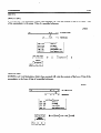
1
Chapter
51
0
5
Programming
GE&90842
SECTION 1
Introduction to Programming
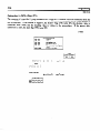
General Information
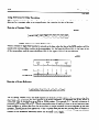
The Series Onem and Series One TM Plus are easy to use small PCs with many advanced features. One
of the advantages of these PCs is the ability to be programmed or tailored specifically to the needs of an
application. Furthermore, if requirements change, the PC can be reprogrammed to fit the new application. This chapter provides the information a user needs to develop or modify the logic within the Series
One or Series One Plus. It will discuss the basics of CPU operation necessary to develop a proper logic
program, the theory behind each function, examples of how that function could be used, and
step-by-step entq of sample programs.
Planning a PC System
When planning a PC system, the first step should be to define the system by writing a description of the
functional requirements for that system. A description would usually consist of block diagrams and
written descriptions of the various parts of the system. Input devices should be defined along with the
process or machines to be controlled. The next step would be to develop the program required to control
the system.
On a sheet of paper, layout each rung of your ladder diagram and assign references to inputs and
outputs. The program can also be written in mnemonic form (Boolean), which is how it will be keyed
into the Series One or Series One Plus when using the hand-held programmer. As an option, programs
can be entered in ladder diagram Format using the Portable Programmer. This applies to both the Series
One and Series One Plus. You can also enter programs with the Workmaster@ industrial computer
using Logicmaster~l application software. For information on using the Wockmaster industrial computer for programming, refer to the Logicmaster 1 Programming manual, GE&96632 for Series One.
For Series One Model E, Series One Plus, and Series One Plus 3.7K, refer to GFK-0075 which is the
Logicmaster 1 Family Programming Manual.
How to Use This Chapter
This chapter is divided into 3 sectiuns. Section 1 is a description of the requirements for programming.
Included, are lists of all of the progr amming functions and a table of programming references assigned
to each slot for 8 point modules. The purpose and types of references are explained, including “real
world” use and internal use. A basic explanation of the scanning operation of the Series One and Series
One Plus PCs is given. The scanning process is the basis for operation of all PCs and the user should
have a good working knowledge of this operation.
The next 2 sections are devoted to programming. Section 2 describes and gives examples of the basic
ladder diagram functions. Section 3 provides the user with a description -f the data operation functions
for use with a Series One Plus PC. The data operations greatly r=xtend ‘LI’pe number and complexity of
applications possible with the Series One family.
520
PrograIIlming
_
GEK-90842
Table 5.1 lists the basic ladder diagram fimctions for the Series One and Series One Plus. A more
detailed explanation of each instruction can be found later in this chapter. Execution times in Table 5.1
are for Series One Model E, Series One Plus, and Plus 3.7K only. Execution times for Series One are
listed in Table 5.2. Note that in the table, VO = I/O points, IR = Internal Relay, SR = Shift Register.
Table 5-l. Series One Model E/One Plus Basic Ladder Diagram Instructions
IIlStruCtiOIl
DdiIlitiOIl
ISTART.
STR
Start rung with a N.O. Normally Open) contact.
1
I
START TIMER.
STRTMR
66
5019
6.6 I/O,IR,SR
I 50.9 Sequencer
Start rung with a N.O. contact referencing a
timer.
START COUNTER.
YrRcNT
Start rung with N..O. contact
1
referencing a counter.
YIR NOT
START NOT.
contact.
STR NOT TMR
STR NOT CNT
Start rung with a N.C. (Normally Closed)
1START NOT TIMER. Start rung with a N.C. timer contact.
IcontacL
I
START NOT COUNTER.
Start rung with a N.C. counter
Add a N.O. contact in series with the previous contact.
1
1
1
Add a N.O. timer contact in series with the
I
I
ANDTMR
1
AND TIMER.
10.3
10.3
I
I
I
I
1
I
91
6115
12.8
12.8
53
612
I
I
I
I
9.1 IJO,IR,SR
61.5 Sequencer I
112.8
I
12.8
_
5.3 I/O,IR,SR
59.1 Sequencer I
previous contacL
ANDCNT
AND COUNTER.
Add a N.O. counter contact in series with
the previous contact.
AND NOT
Add a N.C. contact in series with the previous contact.
1
AND NOT TIMER. Add a N.C. timer contact in series with
1
I the previous contact.
~~
AND NOT CNT AND NOT COUNTER. Add a N.C. counter contact in series
I with tbe previous CantacL
1
OR
1
I
_~
Add a N.O. contact in parallel with the previous contact.
-T---OR TIMER.
OR TMR
~~
OR CNT
OR NOT TMR
84
84
84
.
.
84
Add a N.O. timer contact in parallel with the
previous contact
IAdd
I
I
OR COUNTER. Add a N.O. counter contact in parallel with
the pmious
OR NOT
8.4I/O,IR,SR
60.3
Sequencer
I
.
.
I I
I I
I
I
AND NOT TMR
.
84
ContacL
a NC. contact in parallel with the previous contact.
1
OR NOT TIMER. Add a N.C. timer contact in parallel with
1
the previou!L
I
I
91
612
.
91
I
I
9.1 l/O,IR,SR
625 Sequencer
91
.
I
I
Programming
GE&90842
Table 5-l. Series One Model E/One Plus Basic Ladder Diagram Instructions - Continued
Execution Time
(mhoseconds)
For !&&es One Pins
IIlStI=UtiOIl
D&litiOIl
Memory ,
Words Inactive
Active
OR NOT CNT
OR NOT COUNTER. Add a N.C. counter contact in parallel
with the previous contacL
ANDSTR
.
AND STORE. Connects a logic group in series with the
1
38
logic group preceding it.
1
.
OR STORE. Connects a logic group in parallel with the
38
logic group pceding it.
MASTER CONTROL START. Begin control of a block of
1
5.0
logic with a master control relay.
1
MASTER CONTROL RESET. Ends control of a block of
3.0
logic with a master control relay.
.
Defines a coil for a rung of logic, either an external output or
1
75
an intemal coil.
Defines a coil as being latched, the coil will remain on until
1
17.5
tumed off by RST.
IF ON, the coil will remain ON even under control of the
1
10.0
Output Disabler Coil (376).
--1
.
RESET. Causes a coil that had been latched (SET) to be
93
unlatched (Reset).
1
19.3
SET OUT RESET. Defines a coil as being a one-shot (ON
for one scan).(One Plus Only)
27.1 700.0
‘ITMER. Programs a Timer operation. Times up kom zero
to a preset value. Elapsed time stored in an accumulate
UOJR,SR
458.8 Register
register. Preset time range is 0.1 seconds to 999.9 seconds.
27.1 706.8
COUNTER. Programs an up counter. Counts up from zero
to a preset value which can be 1 to 9999. The cunent count
VOJRSR
465.6 Register
is stored in an accumulate register. Counters are retentive.
Requires 2 rungs of logic; fkst rung enables the counter, the
second rung resets the counter.
53.1 64.1
Sm REGISTER. Programs a shift register which can be
+16.6 For each
128 steps in length or a number of shift registers of varying
lengths (128 bits total). Retentive. Requires 3 rings of logic;
bit shifted
(1) da@ (2) docl& (3) mset. can be pmgrammed to shift
fonwud or bachward.
OR STR
MCS
MCR
OUT
SET
SET OUT
1
91
.
9.1
l
RST
SET OUT RST
SR
Note: I/O = I/O Points, IR = Inuzmal Relay, SR = Shift Register
Table 5.2 is a list of execution times for the Series One functions. Execution times are given in
microseconds.
Programming
GE&90842
Table 5.2. Series One Execution Times
-I===
I/O Point Int Relay
IIlSWUCti0n
33.9
36.5
36.3
38.7
40.8
42.0
38.1
38.1
AND NOT
OR
OR NOT
STR
STR NOT
SET
RST
I
Shift Register Timer Counter
32.7
35.1
34.5
36.9
39.6
432
42.6
42.6
Inactive
Active
36.0
40.8
36
40.8
89.4
97.2
84.0
88.8
84.0
88.8
89.4
97.2
37.5
39.9
43.5
45.6
48.0
50.4
Inactive
Active
MCS
MCR
SET OUT
OUT
35.2
37.8
49.8
43.8
69.6
SR
ANDSTR
OR STR
55.2
34.2
37.8
35.2
37.8
49.8
43.8
115.8
103.5
66.9 + 12.9!/N (1)
34.2
37.8
LnSWUCtiOIl
80.4
11) N = number of bits shifted.
Table 5.3 is a list and description of the data operations that can be programmed, with a Series One Plus,
in addition to the basic ladder diagram functions listed in Table 5.1. A more detailed explanation of
each instruction is provided later in this chapter.
Table 5-3. Series One Plus Data Operation Instructions
Memory
&ion Time
croseconcls)
Active
words
Inactive
2
6 .3
321.9 I/O,IR,SR
80.7 Register
14.3 constant
DATA STORE 1. Loads the lower byte (least significant) of
the accumulator with the contents of a specified 1 byte
reference.
2
6 .3
140.9 I/O,IR,SR
63.8 Register
De STR2
e52)
DATA STORE 2. Loads the lower 4 bits of the accumulator
I witMheupper4bitsofa~lbyte~ference.
2
6 .3
D.STR3
eS3)
DATA STORE 3. Loads the lower 4 bits of the accumulator
I with the lower 4 bits of a spedied 1 byte nsfmnce.
2
6 .3
Instnrcti0n
DGIR
CW
DG’IRl
eS1)
DdhitiOIl
STORE. Loads accumulator with a binary or BCD
I DATA
value which can be a 4 digit castant orthecontentsofa
I
specified 2 byte reference.
I
I
I
~~
,172.2 I/OJEZ,SR
95.0 Register
I
I
Il73.8 I/O,IR,SR
196.6 Register
0
55
Programming
GEK-90842
Table 5-3. Series One Plus Data Operation Instructions - Continued
Execution Time
(microseconds)
Memory .
InstractiOIl
D4&litiOIl
Words badive
Active
DGTRS
(F55)
DATA STORE 5. Loads accumulator with a binary or BCD
value from tbe 2 byte contents of a 16 circuit (high density)
Input Module.
2
.
63
325.0 16 Point
input
Module
D.OUT
(F6W
DATA OUT. The contents of the accumulator (2 bytes) ~RZ
written to a specified 2 byte refkrence (Output, Internal Relay,
Shift Register Coils, Data Register or T/C Accumulate
Register).
2
6.3
329.4 I/O,IR,SR
52.6 Register
D.OUTl
F6l)
DATA OUT 1. The contents of the lower byte of the
accumulator are written to a specifkd 1 byte reference (Output,
Intemal Relay, Shift Register or Data Register.
2
63
.
160.1 I/O.IR,SR
39.1 Register
DeOUT2
(F62)
DATA OUT 2. The contents of the lower 4 bits of the
accumulator are written to the upper 4 bits of a specified 1
byte reference (Output, Intemal Relay, Shift Register or Data
Register).
2
.
63
116.0 I/O,IR,SR
39.8 Register
D.OUT3
F63)
DATA OUT 3. The contents of the lower 4 bits of the
accumulator are written to the lower 4 bits of a specified 1
byte reference (Output, Internal Relay, Shift Register or Data
Register.
2
63
108.1 I/o, IR,
SR
55.0 Register
DoOUT
(F65)
DATA OUT 5. The contents of the accumulator (2 bytes) are
written to a specified 2 byte refierence. Must be a 16 circuit
(high density) Output module.
6.3
365.3 16 Point
=<
On@
COMPARE. The contents of the accumulator are compared to
the contents of a specified 2 byte refe=nce (I, IR, SR, or DR)
or a 4 digit BCD constant. Intemal coils turn on to reflect the
result of the comparison.
Act > DataOn 772
Ace = DataOn 777
Act < Data011 774
.
63
354.0 UO,IR,SR
112.8 Register
57.0 constant
+
(F71)
ADDITION (BCD). The contents of the accumulator are
addedtoa4digitBCDconstantorthecontentsofaspecified
2 byte reference which must be a valid BCD number (Input,
Int~mal Relay, Shift Register or Data Registers).
2
.
63
698.0 I/O,IR,SR
456.8 Register
262.0 Canstant
SUBTRACI’ION (BCD). The contents of a specified 2 byte
&hence (Input, Internal Relays, Shift Register, or Data
Registers) or a 4 digit BCD constant are s&tract& from the
ca@nts of the accumulator.
2
6.3
557.0 IfO,IR,SR
3 15.8 Register
275.0 Constant
MULWPLICATION (BCD). The contents of tbe accumulator
zuc multiplied by he contents of a specified 2 byte reference
(Input, Internal Relays, Shift Register, or Data Registers) or a 4
digit BCD COI~SUII~. ‘Ik lower 4 digits of the result remain in
tk accumulator, the upper 4 digits a~ stod in registers 576
and 577 which is the auxilhy accumulator.
2
6.3
497 to 2851
CYO&SR)
29oto2644
(Register)
223 to 2576
(Constant)
I
Cnz)
X
(F73)
l
output
Module
506
Programming
GEK-90842
Table 5-3. Series One Plus Data Operation Instructions -
Continued
Execution Time
(miuosecods)
lIMNCti0n
lMIlitiOIl
Memory .
Words Inactive
Active
DIVISION (BCD). The contents of the accumulator 8lre
divided by the contents of a specifkd 2 byte reference (I, IR,
SR,orDR)ora4digitBCDconstant. Thefirst4digitsofthe
answer are stored in the accumulator and the remainder is
stored in the remainder is stored in the auxiliary accumulator
(registers 576 and 577).
63
.
DATA AND (Logic product). The contents of the accumulator
are logically AND-ed with each corresponding bit of a
specified 2 byte reference (I, Ilk, SR, or DR) or a 4 digit BCD
constant. The result is stored in the accumulator.
.
63
345.0 IJO,IR,SR
103.7 Register
55.6 Constant
.
63
345.0 I/O,IR,SR
103.7 Register
55.6 Constant
SHIFT RIGHT FUNCTION 80, SHIFI’ RIGHT N BITS. Contents of the
accumulator are shifted to the right by the specified number of
cF80)
bits (l-15). Positions from which bits were shifted are filled
with zleros.
.
63
216 + 13.4/N
of bits shified
SHlFT LEFT
(F81)
FUNCIlON 81, Shill: Lm N BITS. Contents of the
accumulator are shifted to the left by the specified number of
bits (l-15). Positions from which bits were shifted are filled
with zeros.
63
.
DECODE
(F82)
FUNCTION 82, DECODE. Decodes the lower 4 bits of the
accumulator to a decimal number from 0 to 15 and places a 1
in the bit position in the accumulator which comxponds to that
decimal number.
1
.
63
56.3
ENCODE
(F83)
FUNCTION 83, ENCODE. Encodes a bit in the accumulator
to a binary code representing the position number (0 - 15) and
places the binary code in the lower four bits of the
accumulator.
1
63
.
282.0
INVERT. The 16 bits of the accumulator a~ inverted; i.e., 1
to 0 and 0 to 1. Example:
1101 1001 0110 0111
inverted to
0010 0110 1001 1000
1
.
63
30.3
BIN
VW
BINARY. Converts a BCD value in the accumulator to a
binary code.
1
6.3
412.2
BCD
(F86)
BINARY CODED DECIMAL. Converts a binary code in the
accumulator to a BCD value.
1
6.3
746.0
1
6.3
355.3 I/OJR,SR
114.0 Register
722 Constant
.
F;4)
DdND
(F7S)
DoOR
(F36)
DATA OR (Logic Sum). The contents of the accumulator are
logically OR-cd with each corresponding bit of a specified 2
byte reference (I, IR, SR, or DR) or a 4 digit BCD constant.
The result is stored in the accumulator.
ENTERNAL FUNCI’ION 2 0 , EKIZRNAL, FAULT DIAGNOSIS. Allows
FAULT
extemal &vices to be monitored for unwanted conditions. If a
DIAGNOSIS
fault occurs a presssigned 4 digit BCD number is displayed on
the programmer. Multiple fault conditions can be monitored.
0)
1218 to 2851
(I/o, IR, SR)
742 to 2645
(Register)
720 to 2577
(Constant
2
_
220 + 13.4/N
of bits shifted
Programming
?
GE&90842
Programming Fundamentals
This section provides a guide for entering and using each of the instructions. The instructions are
presented in groups that correspond to their functionality. Table 5.4 lists the instructions grouped in this
manner.
Table 5-4. Series One/One Plus Instruction Groups
BASIC INSTRUCTIONS
STR, STR TMR, STR CNT, STR NOT,
STRNOTTMR,S'IRNOTCNT
AND,ANDTMR,ANDCNT,ANDNOT,ANDNOTTMR,
ANDNOTCNT
OR,ORTMR, ORCNT, ORNOT,ORNOTTMR,
ORNOTCNT
ANDSTR, ORSTR
MCS, MCR,
OUT, SET, SET OUT, RST, SET OUT RST (ONE PLUS ONLY)
TMR, CNT, SR
DATA OPERATIONS
SERIES ONE PLUS ONLY
MOVE
DGTR (FSO), D.STRl (FSl), DCI’R2 (F52)
D.STR3 (F53), DoSIR (F55)
DaUT (F60), D.OUTl (F61), D+OUT2 (F62)
DKNJT3 (F63),D.OUT5 (F65)
ARITHMETIC
>=< (FIO), + ml), - F72), x F73), f (F74)
DAND (F75), DoOR (F76), INV (F84)
LOGICAL
CONVERT
BIN (F85), BCD (I?‘86), Shift Right (F80)
shift Left, (F81) Decode (x%2), Elmode (F83)
SPECIAL
Extemal Fault Diagnosis (RO)
Significance of References
Whenever programs are entered into any PC, they must be accompanied by reference numbers. These
references help to tell the CPU which function is specified. For example, which pushbutton controls the
starting of which motor? Which timer are you referring to? Reference numbers are a vital part of
programming, and in the Series One and Series One Plus are octal based; that is, they start at 0 and go
up to 7, then jump to 10; at 77 the next value is 100. They look like traditional decimal numbers, except
the digits 8 and 9 do not exist. Table 5.5 summa&e s the various reference values and their signifkance.
Programming
58
0
GEL90842
Table 54. Summary of References
Octal values
Rt!&THlCeS
000-157
000-157
700-767
770-777
160-337
I/O points (Series One)
I/O points (Series One Plus)
(Series One Plus only)
Special Function Coils (Series 0~ Plus only)
Intemal Coils (Non-retentive)
340-373
374-377
400-577
600-677 (4)
Retentive Coils (Internal)
Special Functions
Shift Registers
Timers and/or
Counters
Data Registers, M-bit (Series One Plus only)
400-577
WQnantits
112 total
168 total
8
112
28
4
128
64
(1)
(1)
(1)
(2)
(1X2)
64 WV
124 Total if T/C references used as data registers
1. Retentive upon power failure.
2. Total maximum number of Timers and/or Counters.
3. Shift @ster and data register references are identical however, shift registers operate on bits, while data registers (located in a
Merent area of memory) operate on bytes.
4. T/C references 600-673 can be used as data registers, if they are not referenced as timers or counters.
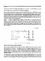
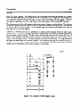
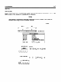
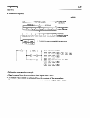
Significance of Input/Output References
I/O modules can be placed in any mix desired; however, once installed the exact reference used in
programming is established by their physical placement. In other words, references are assigned to each
location by the operating system in the CPU, and therefore E fixed for each location. As shown in the
example in Figure 5.1, the modules are numbered from zero (adjacent to CPU) towards the left through
all racks until the last module is reached at the left of the last rack. The exact reference is obtained by
appending the circuit number (O-7), to the module number. Circuit numbers depend upon the terminal to
which the field device is wired as discussed in Chapter 6. Table 5.6 summarizes available I/O references
for 8 circuit modules for your convenience. This table can be reproduced locally to form a part of your
system documentation. Notice that whether reference 005 is an input or an output depends upon which
module is inserted into the I/O slot adjacent to the CPU. Refer to the Series One family compatibility
guide in Appendix C for additional valid If0 references per physical location of modules.
Programming
GEL90842
L li
ml
TO
107
/
A
070
TO
077
c
a
10
040
TO
057
047
150
TO
157
I40
TO
147
-a
&
TO
067
L
040
A
a40797
130
TO
137
‘r
J
030
TO
107
r
1
a
a
L
3
I
1
TO
057
TO
047
TO
037
020
TO
027
TO
007
150
TO
157
140
TO
147
130
TO
137
120
TO
127
loo
TO
107
-I
CPU
t
l
. 5
7
I
10 SLOl RACKS
IEXAMPLE SFRYS ONf PLUS)
k
1
02
f
’
01
20-27
lo-17
120-127
110-117
t
I
J
I
T
3
T
I
00
SLOT NUMBER
o-7
vo
12
REFERENCE
'
~
5SLOT RACKS
(EXAMPLE-SERIES ONE)
Figure 5-l. I/O References Per Physical Placement for 5 and lo-Slot Racks
NOTE
The addressing of slot 10 in a lO-slot rack is determined by configuration of the two bridge
connectors on the rack backplane.
S-10
Programming
GE&90842
Table 5-6. Summary of I/O References for 8 Circuit Modules
Mociule No.
00
01
02
03
04
05
06
Circuit No.
0
1
2
3
4
5
6
7
Reference
au
002
003
005
an
0
1
2
3
4
5
6
7
010
011
0i2
013
014
015
016
017
0
1
2
3
4
5
6
7
020
021
022
023
024
025
026
027
0
1
2
3
4
5
6
7
.030
031
032
033
034
035
036
037
0
1
2
3
4
5
6
7
040
041
CM2
043
0
1
2
3
4
5
6
7
050
051
052
853
054
055
056
057
0
1
2
3
4
5
6
7
045
046
047
061
062
c&3
065
066
c&7
hmut
Device Name
Wire No.
Programming
Table 5-6. Summary of I/O References for 8 Circuit Modules - Continued
Module No.
07
10
11
Circuit No.
Reference
0
1
2
3
4
5
6
7
070
071
072
073
074
075
076
077
0
1
2
3
4
5
6
7
100
101
102
103
104
105
106
107
0
1
2
3
4
5
6
7
110
111
112
113
114
115
116
117
120
121
122
123
124
125
126
127
13
14
15
0
1
2
3
4
5
6
130
131
132
133
134
135
136
0
1
2
3
4
5
6
7
140
141
142
143
144
145
146
147
0
1
2
3
4
5
6
7
150
151
152
153
154
155
156
157
InOut
Device Name
Wire No.
~-
5-12
GEL90842
Table 5-6. Summsiry of I/O References for 8 Circuit Modules - Continued
Module No.
70
71
72
73
74
75
76
Circuit No.
Reference
0
1
2
3
4
5
6
7
700
701
702
703
704
705
706
707
0
1
2
3
4
5
6
7
710
711
712
713
714
715
716
717
0
1
2
3
4
5
6
7
720
721
722
723
724
725
726
727
0
1
2
3
4
5
6
7
730
731
732
733
734
735
736
737
0
1
2
3
4
5
6
7
740
741
742
743
744
745
746
747
0
1
2
3
4
5
6
7
750
751
752
753
754
755
756
757
0
1
2
3
4
5
6
7
760
761
762
763
764
765
766
767
In/out
Device Name
Wire No.
,~
Programming
5-13
GEK-90842
Internal Coils
The internal coils are control relays that can be used to control logic in the Series One or Series One
Plus user program. However, their status cannot be provided directly to the I/O section. Retentive
relays are specialized internal coils that have their ON or OFF status retained during time periods that
the PC is not operating such as during loss of AC power. They use dual operations (set and reset) similar
to hard-wired latching relays. A switch (Sl) on the CPU module must be set to the ON position in order
for the internal coils, 340 to 377, to be retentive upon loss of power. If the switch is not set properly,
these coils will function as non-retentive coils.
Use of the Special Function Coils
Internal coils 374 through 377 are special purpose coils, in that they always perform specific internal
functions and also provide useful internal system status. Coil 374 is a fist scan reset or power-up
indicator. Coil 375 provides a convenient way to program a 0.1 second clock pulse. Coil 376 can be
used to inhibit all hardware outputs, that is, outputs that are connected to user devices (programmed with
an OUT m instruction). Finally, coil 377 is an indicator of the operating status of the back-up battery
for the CMOS memory devices. This coil could be used as a contact to turn on an output connected to a
light, bell, etc. as a visual warning of a low battery.
Shift Register References
A group of references (400 to 577) are used by the shift register. A total of 128 stages are possible and
they can be used as one large shift register or a group of smaller shift registers (for example, 3 @ 30
stages and 2 @ 19 stages) as long as the total number of stages does not exceed 128. Additional details
on all these functions will be provided later in this chapter.
Timer and Counter References
Another group of fixed references (600 to 677) are used with timers and counters. Any mix of timers or
counters totaling 64 can be used in a Series One or Series One Plus PC. Counters provide an additional
function, in that they can also control a sequencer with up to 1000 steps. Counters are retentive upon
power failure. References 600 to 673 can be used as 16.bit data registers if they are not used as T/C
references. T/C references 674-677 are reserved for Thumbwheel Interfaces or Timer/Counter Set Point
use only.
Data Registers
Data registers are available only with a Series One Plus PC. This is a group of sixty four 16-bit registers
which can be used for storage of numerical data. Data can be written to or read from the data registers
for use by the data operation instructions. Additionally data stored in the regkters can be used as
Timer/Counter presets. The references to be assigned to these registers are 400 to 577. Note that these
references are identical to the shift register references. However, shift registers operate on individual
bits (4(X),401,402, etc.), while the data registers operate on bytes and are located in a totally merent
area of memory. A byte in the Series One Plus PC is a group of 8 consecutive bits and each register is 2
bytes in length. By using available T/C references, the total number of data registers references can be
up to 124.
5-14
Programming
Flexibility in Using References
Although references are assigned to specific functions as shown in Table 5.5, there is some flexibility in
their use. I/O references not used by the hardware I/O section (for example, no module inserted into
that slot or circuit not wired up) can be used as internal coils. However, if expansion is planned for the
future, sufficient references to support that expansion should be reserved and not used in the current
programming. Retentive coils can also be used as internal coils if their retentive function is not
required. However, typically the unique value of retentive relays does not justify their sacrifice for a few
internal coils. The shift register references can be used as a source for additional retentive or internal
coils if they are not used for shift registers or sequencers.
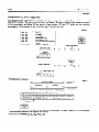
Operating Principles
Before discussing the details of programming and the use of references, some details on the internal
operation of the CPU can be useful. The majority of Series One and Series One Plus applications can be
solved and the programs developed without consideration of the internal structure of the CPU. However, some applications can be more efficiently solved if knowledge of the CPU operation is applied
while the program is being developed. The basic operation of virtually all PCs is referred to as a
scanning function. There are many hundreds of decisions to be performed in any program, and the CPU
cannot do all of them simultaneously. Similar to any electronic processor, it performs its operations one
at a time. However, the speed of performance internally, makes the external results appear to have all
operations accomplished at once.
scanning
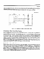
The term scan is a method of describing how the CPU performs its assigned tasks (see Figure 5.2). It
begins at the first function, such as a relay contact, entered into the beginning of memory (address 0000).
It proceeds sequentially through all memory addresses performing all functions entered by the user (for
example, relay contacts, timers, latching relays, counters, sequencers, shift registers, etc.) until it reaches
either the end of memory (address 1723) or the end of the program as entered by the user.
During the scan the logic sets or resets coils, according to the instructions entered into the logic program
by the user. The status of these coils is immediately available to the next logic function. At the end of
the logic scan, the CPU gets input data from the input modules and provides new data to output
modules.
Next, the programmer, if connected, is serviced by making logic changes and/or updating its display.
After servicing the programmer, the CPU performs a check of its internal hardware and resets the
watchdog timer. The watchdog timer is a hardware timer set at 180 msec (milliseconds) to ensure that
memory or internal circuit faults do not cause the CPU to enter an endless loop because of hardware
failure. If a scan is not completed at least once every 180 msec (typical maximum scan is 60 msec), the
hardware will shut the CPU down turning outputs OFF. Finally, any forced I/O wiIl be entered. With
successful completion of the internal checks, the CPU goes back to the start of the scan and continues its
scanning sequence with the logic function entered at address 0000. This repetitive scanning operation is
performed from the time power is applied to the CPU until it is removed.
Total scan time includes user logic solution time plus overhead. The overhead time includes monitoring
functions, I/O updates and housekeeping tasks. The typical scan times listed in the specifications in
Chapter 1 assume that only basic instructions have been programmed (AND, OR, STR, NOT, etc.), they
do not include overhead. The overhcti time is about the same (4 to 5 mSec) for Series One and Series
One Plus. This time must be added to the logic solution time to obtain the total real scan time.
515
Programming
GEK-90842
In order to achieve the maximum scan time, the monitor function should be disabled for both Series One
and Series One Plus programs, since the monitor function adds about 2 mSec of overhead time when it
is active. Also the overhead of a Series One Plus is increased slightly when communicating through the
DCM, since both the Series One Plus CPU and DCM have been designed to provide a much higher
throughput than the Series One CPU/DCM combination. Additionally, timer and counter instructions in
the Series One Plus are slower than in the Series One because of the ability to use registers for preset
values.
The scanning operation is very basic to PC operation and should not be overlooked. It provides a very
useful verification of the CPU’s reliability. For details on troubleshooting, refer to Chapter 7. The
scanning operation also provides a fixed and definable sequence of logic decisions. Functions are solved
in the order programmed. The results of one function (for example, coil, timer, shift register, etc.) are
immediately available internally to the next logic element. In larger complex logic programs, internal
races can be eliminated. The user does not need to be concerned with the time delay relays required to
pull in or activate nor their variations (for example, a 4 pole vs 8 pole relay).
SOLVE
LADDER
MAGRAM
SERVICE
r/o
SERVICE
PROGRAMMER
WATCHDOG
TMER
ADD FORCED Vb
Figure S-2. CPU Scanning Sequence
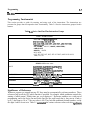
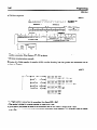
Programmer Functions
The basic programming language of the Series One and Series One Plus PCs is a simple relay ladder
representation based upon standard Boolean functions (AND, OR, and NOT). Throughout the discussion of programming, examples will be used to illustrate the function described. The illustration of the
Programmer (Figure 5.3) will be used as a reference for these examples and specific key sequences will
5-16
Programming
GEK-90842
be provided so that the user can follow and demonstrate the example. A short-hand notation will also be
provided that is recommended as a simple method to document your program. A complete discussion of
the programmer is provided in Chapter 4. A brief overview of important keys is presented below to aid
the user’s understanding of the examples.
The keyboard has both upper and lower case functions similar to a typewriter. The numerical keys for
most programming steps are accessed by first selecting the SHF (Shift) key to the upper right. Once
depressed, the SHF LED is lit (display center right) and then the appropriate numerical digit(s) can be
selected. The shift function is latched and will be released only by selection of the ENT (Enter) or CLR
(Clear) key. The SHF key does not have to be held down. The display window in the upper left reflects
either address or data information (not both) as the operation progresses. Typically, as keys are selected,
their resmctive LEDs will light to display the function selected. Other important keys are as follows:
KEY
AND
OR
STR
NOT
OUT
TMR
CNT
SET
MCS
MCR
SR
RST
F
R
FUNCTION
AND referenced status with previously entered logic (Series)
OR referenced status with previously entesed logic (Parallel)
START new rung of a ladder diagram
NOT or invert (i.e. make normally closed) contact referenced
OUTput logic status to a coil, either output or intemal
TIMER is selected as desired function
COUNTER is selected as &s&d function
SET latching relay or shift register status
Master Control Start - begin control of master control relay
Master Control Reset - end control of master control relay
Shift Register - establish range of shift register
RESET latching relay or shift register status
FUNCTION - specifies a data operation (Series On& Plus)
REGISTER - specifies a data qister or group entry (Series One Plus)
a41 939
Figure 5-X Programmer for Series One and Series One Plus
Programming
5-17
_~
GEL90842
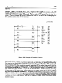
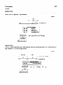
Basic Ladder Diagram Format
Figure 5.4 illustrates a typical ladder diagram. Between two vertical power rails to the extreme left and
right, contacts are placed in horizontal strings or lines. Adjacent lines can be connected between
contacts by a vertical line to allow logic to be solved in parallel. The horizontal strings (series) of
contacts anz equivalent to ANDs. For example line 1 can be described as: A and B and C must occur
before coil X is energized; any one reference can prevent the coil from energizing. Similarly vertical
contacts are in parallel and programmed as ORs. Thus, line 2 is described as: D or E or F will energize
coil Y. Any one reference can by itself energize coil Y.
In the Series One and Series One Plus PCs, there is no internal limit on how many contacts can be
placed in series, nor how many in parallel. However, as a practical limit for simple programming and
system documentation, it is recommended that a horizontal string be limited to nine contacts and one
coil; and a vertical array to seven parallel lines.
a42342
D
E
F
It
v
-
0
OUTPUT f
COIL
RlGuT
POWER
RAIL
-
’
LEU
POWER RAIL
Figure S-4. Typical Ladder Diagram
Concept of Power Flow
One key feature of PCs is power flow. This is a conceptual flow of power used to visualize the operation
of coils, timers, counters etc. Referring again to Figure 5.4, the left hand power rail can be envisioned as
“hot” (connected to 115 V ac or +24 V dc) and the right as its associated “neutral” (connected to 115
V ac or -24 V dc), The coils (e.g. X and Y) will be energized if there is a path for power flow from the
left leg to the coil placing the full potential across the coil. If there is no power (electron) flow, the coil
will be de-energized (OFF).
Power always flows from the left towards the right and will pass through normally open contacts if their
references are energized (ON) or normally closed with de-energized (OFF) references. Power flow is
also allowed vertically either up or down between adjacent lines where parallel connections are
programmed. However, power can NOT flow from right to left at any time through contacts or
horizontal shunts. ‘I&s feature simpWes programmin g and prevents undesired sneak paths. However,
if hard wired relays are replaced by a Series One or Series One Plus PC, it is possible some adjustments
may be necessary to the logic to either simplify the programming or to add sneak paths that may be a
basis for the relays functioning.
5-18
Programming
GEK-90842
Unlimited References
Another difference between PC programmin g and hardwired relays is that any reference such as an input
or coil can be used on relay contacts as often as necessary. Since references are merely a unique series
of bits in a word of memory, they can be programmed wherever and whenever necessary. Now with
PCs, there is no need to count relay contacts and try to limit individual references to four or less
contacts; no need to plan to use form C relay configurations to squeeze two contacts from one pole. Any
reference can be envisioned as a relay controlling many poles providing both normally open and
normally closed contacts that operate without any time delay from pole 1 (closest to the coil) to pole
1000 (furthest away from coil).
Programming
5-19
GE&90842
2
Basic Instructions
SECTION
Basic Instructions
This group can be considered as the basic building blocks for a relay ladder diagram. The instructions
reference discrete bits that are to be part of an operation, that is, a conditional contact or the end of a
rung, which could be an output or an internal relay.
How to Begin Programming
The easiest way to begin feeling comfortable with programming a Series One or Series One Plus PC, is
to enter one rung of logic with contacts in series that control a single coil. Physically connect input
devices (pushbutton switches, limit switches, etc) and an output device (such as a lamp) to the
corresponding terminals on an input and output module in the PC, turn the inputs on and off, and observe
the result on the output device.
Entering a Rung With Series Contacts
In the following program sequence, a rung of ladder logic is shown, then the keystroke sequence
required for entering the logic. Notice that when entering a numerical sequence, the SHF key must be
depressed before the number or number sequence. In the example, each keystroke is separated by a
comma. Numbers with more than 1 digit are grouped together for ease of interpretation.
Turn the mode keyswitch to the PROG (programmin g) position in order to enter the logic.
Enter wo normally open contacts (1 and 2) in series controlling the state of an output coil (17). Both
contacts must be closed to tum on the output.
a40347
When input devices wired to inputs 1 and 2 are closed, output 17 will tum on. The operating state of the
inputs and outputs, either ON or OFF, can be monitored by observing the LEDs on the Programmer’s
logic display that correq3ond to the input or output.
Entering the Clear all Memory Sequence
After observing the operation of the series rung, the rung can be deleted by entering the clear all
memory sequence, or the rung can remain in memory, with the next rung starting at the next memory
address. The next memory address, assuming that tEre above rung was entered at address 0000, is 0003.
If you wish to clear tie contents of memory and , start the next rung at address 0000, enter the following
key sequence.
CLR, SHF, 348, DEL, NXI’
5-20
Programming
GEK-90842
When the clear all memory sequence has been successfully entered, the rung of logic that had been
entered will be cleared from memory. (Remember, whenever the clear all memory sequence is entered,
the entire contents of memory will be cleared).
NOTE
Be sure that you want to clear the complete contents of memory when using this sequence, there
is no recovery.
Entering a Rung with Parallel Contacts
Continue the simple program entry by entering a normally open contact (4) in parallel with a second
nomally open contact (20) that references the output coil (20). In series with these, add a normally
closed contact (5), then the output coil.
a40347
If an input device, such as a limit switch is wired to input 4, and the limit switch is closed, the output
would turn on. The normally open contact referencing the output would close and become a seal
contact, which would maintain the output in the on state, even if the limit switch wired to input 4 were
then opened. The output could be turned off, in this example, by momentarily closing a switch
connected to the closed contact, reference 5. Since this is a normally closed contact, it would open when
the switch is depressed, and the output would turn off. This logic is commonly used as a motor starter.
Entering a Simple Timer Rung
Next, enter two rungs of logic, the first ending with a timer, having a preset value of 30 secondsThe
second rung has an output controlled by the state of the timer coil. When input 11 is closed, the timer
begins timing up from 0 towards the preset value of 30 seconds. When the accumulated value of the
preset reaches 30, the timer coil will turn on, contact T605 will close, and output 25 will turn on.
a40347
5-21
Programming
Basic Relay Logic (Motor Starter)
With this background on the basics of pro gramming a Series One and Series One Plus PC, Figure 5.5
provides a simple example to illustrate relay ladder programming. The references used were selected for
illustrative purposes and can be adjusted as necessary to meet your application needs. This is a simple
motor starter and seal circuit. An input module is assumed to be installed next to the CPU (005 = start
pushbutton input, and 006 = stop pushbutton). Adjacent to the input module is assumed to be an output
module (010 = output to motor starter). The program does not care whether these input and output
modules are 115 V ac or 24 V dc. The programmer keys to be depressed to enter this logic are also
shown in the figure. The start key begins a new rung of logic; this example and most that follow assume
an empty memory so the example begins at address 0000.
START
KEY
ON LED’S
STR
I
STR SHF
SW
0
STR
STR. SHF
ADR
STOP
IANdl
0001
ADR
DIS PLAY
AND
SHF ]
AND. NOT. SHF
6
I
AND. NOT, SHF
IF]
ADR
[
I
OR. SHF
oft SHF
ON LED’S
AND. NOT
5
OR
OR, SW
KEY
DtSPLAY
6
0003
OUT
1
I SW
OUT. SHF
10
El 1
OUT, SHF
1
0 0 0.2
00
OUT, SHF
10
EN’I
I
ADR
0 0 0 4
Figure 5-5. Sample Relay Logic (Motor Starter)
Motor Starter Logic Description
The first reference is entered (STR, SHF, 5, ENT) and a normally open contact is established since the
NOT key was not depressed. Referring to Figure 5.5, the next function moving from the left (contact
005) to the right along the top line of the logic rung, is a parallel contact referenced as 010. Parallel
logic is represented by the OR function, which is selected followed by the desired reference (10) and the
Enter key to load the memory. Again moving to the right of the top line, the next contact is in series with
the logic completed so far. Thus the ANTI key is selected (for series logic). Since this contact is
normally closed, the NOT key is also selected followed by the reference 6 and the Enter key.
The final element of this logic is the coil or output of the rung. Selecting the Output key does not ensure
a “real world” output will be generated; it also must refer to an I/D reference and have an output
module inserted in the proper slot. To establish the rung output coil, the output key is selected followed
by the Shift key, the reference (10) and the Enter key. Outputs can be paralleled by entering additional
OUT functions immediately after the initial one.
Programming
5-22
GEK-90842
Normally Closed Input
After completing the logic of Figure 5.5, several features of progr amming should be noticed. First, all
elements of the program are entered directly into CMOS memory as the Enter @NT) key is depressed.
Thus, if power should be interrupted while a program is being entered or altered, it will be totally saved
except possibly for the one element being worked on. Second, there is feedback on the programmer for
all entries. Something happens (LED ON, display changes, error codes appear, etc) for each key
selected. Third, the logic is set up for inputs that are wired normally open. If an input is wired normally
closed, an adjustment must be made to the symbol (NO or NC) used for that input. Referring to Figure
5.6, inputs sense voltage at their field terminals. They can not detect if a voltage is from a normally
open limit switch that is depressed or from a normally closed pushbutton that is not depressed. Cover up
the two field devices wired to inputs 002 or 003. If you were the input module, and both applied voltage
to the field terminals, could you tell which was wired normally closed and which normally open?
Because of this, the programmer or system designer must compensate.
Figure 5-6. Example of Normally Closed Inputs
In a previous discussion, it was stated that inputs are like relays with many poles and you are selecting
which type of pole is to be used when you program. In the lower half of Figure 5.6, coil 002 is shown in
the de-energized position; however it is wired to a normally closed pushbutton. When you want power
to flow if the pushbutton is NOT depressed, which contact type do you choose, NO or NC? The answer
is normally open since coil 002 is always energized except when the pushbutton is depressed. Therefore, in pqGimmin g with the Series One or Series One Plus PCs, a normally open contact is
appropriate. If the stop button of Figure 5.6 were wired normally closed, its internal logic should be
normally open to compensate] However, this concept does not normally cause problems for the
programmer. Since PCs are reprogrammable, if an error is made and discovered when the system is
exercised, it is easy to correct
Programming
5-23
GEK-90842
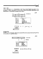
Push-Down Stack
Two very useful functions are programmed using a 2-key sequence, the AND STR and the OR STR.
The AND STR provides a common series connection between a block of logic and the OR STR
provides a common parallel connection for a block of logic. These instructions provide the connecting
links not allowed with any of the previously mentioned instructions. The logic used with this type of
operation is referred to as a push-down stack. The push-down stack can accommodate up to eight levels
(groups) of logic. A push-down stack can be thought of as a temporary storage area to allow the
combining of elements in series (AND) or parallel (OR) connections. Figure 5.7 illustrates the use of
these functions.
a40545
Figure 5-7. AND STR and OR STR Connections
The following pages contain a more detailed description of a pushdown stack and programming with
the AND SIR/or STR instructions.
Programming
S-25
GEL90842
Rule Number 3: The AND STR or OR SIR instructions logically AND or OR location number 1 in
the stack with location number 2 and writes the result into location number 1. In other words, these
instructions put one group of contacts in series or parallel with another group of contacts. This
instruction also moves the contents of positions 3 through 8 up one location.
Rule Number 4: An OUT Y instruction sets Y to reflect the status of location number 1 in the stack. If
the status of location number 1 is ON (I), output Y will be turned off. If the status of location number 1
is OFF (O), output Y will be turned off.
LOCATKIN
NUMBER
1
2
Figure 540. AND STR/OR STR Example Number 1
s-26
Programming
GEK-90842
ED
SIR
f
4
6
ANDNOT
ORSTR
iEFsTR
20
LOCATION
c
4’H’t -
ANDSTR
,
our
20
20
;IH'C
Figure 5-11. AND STR/OR STR Example Number 2
Use of Retentive Coils as Latches
All coils referenced so far have not been retentive upon power failure. Thus if a non-retentive coil is ON
when power is removed fkom the CPU, it will be OFF upon reapplication of power (if Switch 1 on the
CPU module is ON). Them axt 28 special coil references (340-373) that axe retained upon power
failure. Thus if they were ON prior to loss of power, they will be ON when power is restored; they will
be OFF while power is OFF since no scanning is being performed. In addition to these 28 references,
latches can be built using shift register references (400-577) that are not being used to perform shift
register functions. Either retentive coils (340-373) or shift registers (400-577) can be used to control
contacts, both normally open and normally closed wherever required. ‘Ikis special retentive function is
derived from their use as coils to complete or store the results of relay logic rungs.
Programming a Latched Relay
Latches require two separate functions or inputs similar to hard-wired relays, a SET (turn ON) and a
RESET (turn OFF). These functions are commonly referred to as latch and unlatch. If both are active,
the last one in the scan will be controlling the state of the coil. To turn on a latch, the function SET
Programming
527
GE&90842
followed by the retentive coil reference (for example, 340-373 or 400-577) is used instead of OUT, plus
the coil number at the end of a logic rung. Once power flows to that coil, it will be energized (turned
ON) and remain ON even if power flow to it should be interrupted.
To turn a latch off (de-energize) separate relay logic should be built ending in a RST (Reset) function
and the [same] coil number. In many applications, it is useful to allow the system to clear (turn OFF)
coils when power fails so that an orderly restart is possible when power is restored, whether that is 2
seconds or several hours, or several days later. Other applications require the control system to
remember the status of key items such as part position, operations completed, elevators up or down, etc.
The Series One and Series One Plus are provided with both standard and retentive coils to allow the user
to tailor the program to fit their requirements.
Figure 5.12 illustrates the programmin g of retentive (latched) relays. Coil 340 is used only as m
example.
The logic to either set or reset a retentive coil can be of any convenient size similar to
standard coil logic. When power flows through the top rung to the SET coil 340 function, it will be
energized and remain ON even if power flow is removed. Anytime the power flows through the lower
rung (regardless of path), coil 340 will be turned OFF. Since the set coil 340 is programmed before the
reset, it is placed in earlier memory locations and the reset function will have overriding control if they
are both energized.
271
132
037
175
340
STR
AND
OR
OR
STR NOT
AND
OR
AND
SET
STR
AND
STR
AND
RESET OR
SET
067
306
036
340
AND NOT
RESET
271
132
135
377
037
175
267
STR
340
067
306
015
307
SfR
036
340
1 1 14 WORDS PER ELEMENT
1
Figure 5-12. Example of Latching Logic
Master Control Relay Functional Description
To control large quantities of coils on a supervisory basis, a Master Control relay function is provided.
This function allows an efficient method of programmin g to turn off large quantities of coils in case some
major permissive is not satisfied. One approach would be to incorporate a permissive contact in each
rung controlling one of the coils. This may require many contacts and inefficient use of memory.
Another method is to bracket those rungs over which master control is desired; this is similar to
quotation marks around a direct statement (one at each end to define exactly where the statement starts
and where it ends).
The permissive logic is first built starting to the left of the ladder diagram adjacent to the “hot” power
rail. Then an MC!? (Master Control Start) function is entered, followed by the logic it is to control, and
ending with an MCR (Master Control Reset) function. The MCS and MCR axe like quotations around
the logic to be controlled. When power flows to the MCS, the logic enclosed will operate normally. If
548
Programming
GEK-90842
there is no power flow to MCS, the coils will be forced to the OFF state regardless of the internal logic
conditions, timers will be reset to zero, and counters will stop (frozen) but not reset. The amount of logic
controlled by the Master Control relay function is limited only by the memory provided.
STR
AND
MCS
STR
OR
AND
OUT
152
156
010
271
SPAN Of
CONTROL
~+--+t-++-e
265
+--it---u+
043
r
STR
AND
AND NOT
OUT
STR
AND
OUT
-MCR
STR
AND
OR
AND NOT
OUT
003
005
007
043
021
052
152
156
010
271
152
027
265
017
012
315
303
043
1 18 WORDS PER ELEMENT
1
Figure 543. Example of Master Control Relay Logic
Programming a Master Control Relay Function
Figure 5.13 illustrates the use of one pair of MCS/MCR functions. In many cases it is convenient to
view the MCS function as defining a sub-left power rail whose connection to the main power rail is
dependent upon some relay logic. The conditional logic (IO03 - 1125 in this example) is built fkst using
the normal relay logic. The MCS function is entered without any reference to create the beginning point
of the control. Logic is built using normal functions within the control area. Note the duplication of
contact 152, which cost only one memory word, there is no need to count or limit the quantity of relay
contacts used in PCs. To end the master control, the MCR function is entered returning control to the
next power rail to the left and conventional logic can now be built. Unless both references 003 !andA
005 are energized (ON) in this example, coils 052,271, and 265 will be OFF. When these contacts are
passing power, coils 052, 271, and 265 will respond to their normal logic.
Multiple Master Control Relay Functions
Multiple master control functions are possible in any logic program. They can be embedded within the
scope of the first MCS and the last MCR as necessary, as illustrated in Figure 5.14. The f&t group of
coils under the Master Control of references 010 [or] 011 is 204-213 which includes two smaller groups
(207-210 and 212-213). Group 207 and 210 are under the Master Control of 010 or 011 and 015, while
group 212 and 213 are controlled by 010 or 011 and 022. Note the requirement for two successive
MCRs to end both the group 212-213 and the larger group 204-213. To operate correctly there must be
an equal number of MCS and MCR fhnctions in your program.
Programming
5-29
GEK-90842
ST-R
010
011
5
-
OUT
SfR
204
012
205
013
AND Not
014
SfR
MCS
STR NOT
i:
Sm
wr
OUT
[
E
MCA
STR
ANoNof
OUT
STR
MCS
STR
OUT
SfR NOT
ANDNOT
L
r
$i
-MCR
STR
AND
Lbof
Out
I1 22
016
207
012
210
WOROS
023
021
:;:
024
212
025
026
213
030
031
033
032
27:
PER ELEMEN’
]
Figure 5-14. Multiple Master Control Relay Logic
Disabling of Outputs
In addition to Master Control functions, all outputs can be affected by an internal special function coil
referenced as 376. When this coil is energized by user logic, all outputs in the hardware I/O structure
will be turned OFF. Internal coils and statuses will still operate, but only internally. The only exception
is to coils that are programmed as SET OUT functions rather than the OUT function. These will still be
able to provide their normal output status (ON or OFF) to the I/O section.
Figure 5.15 illustrates
the use of coil 376. In this example, when either reference 003 or 056 (inputs,
outputs, or internal depending upon hardware I/O configuration) is energized, coil 376 will also be
energized. This will cause all coils programmed with the OUT function, such as 010, to be turned OFF
at their output module, although they will function normally internally. However, coils driven by the
SET OUT function, such as 011, will not be affected by the status of coil 376. Table 5.7 summarizes the
effectof coil 376 on the OUT and SET OUT functions.
NOTE
It is not recommended that the Output Disabler coil (376) be used with retentive coils (latches).
Table 5-7. Effect of Coil 376 (Output Disabler)
Coil 376 OFF
I
OFF
ON
I
OFF
ON
Coil 376 ON
OFF
ON
5-30
Progra.mming
GE&90842
003
376
II
STR
OR
OUT
STR
OR
ANDNOT
OUT
STR
OR
ANDNOT
SET OUT
?
056
i
0
t
005
It
L
c
006
#
010
010
I I
\
005
003
056
370
005
010
006
010
005
011
006
011
006
SET
I11 00 WORDS PER ELEMENT
Figure 5-15. Sample Coil Disabler Logic
Timer and Counter Functional Description
In addition to relay logic, there are a wide variety of functions that are standard with the Series One and
Series One Plus. Timing and Counting are two of the most commonly used non-relay functions. These
functions are special coils using references 600-677. Up to 64 total timers and/or counters can be built
within the Series One or Series One Plus. They end a rung of logic similar to using an OUT function
for relay logic. Unlimited contacts, both normally closed (timed OFF delay) and normally open (timed
ON delay) can be referenced to any timer/counter coil. A preset value is used to indicate how many
seconds, tenths of seconds, or counts, the function should delay before energizing its coil. When the coil
is energized, time or counts continue to be recorded. All presets can be up to four decimal digits (0001
to 9999), which allow timers to be set from 0.1 to 999.9 seconds, and counters from 1 to 9999 counts.
Timers can be set from 0.01 to 99.99 seconds with the Series One Plus 3.7K PC only. Timers are set to
a .Ol second duration by setting output reference 770 (SET 770). Caution must be used when doing this,
since reference 770 being reset in the same program would cause the timers to revert back to .l second
duration.
Special Timer/Counter References
The four references 674-677 obtain their presets from external thumbwheels
via the thumbwheel
interface. Additionally, a Timer/Counter Setpoint unit can be used with the Series One Plus to enter the
preset values. When a preset value is selected with the Timer/Counter Setpoint unit, the values are
simultaneously entered into &bit registers, (two registers for each 4digit BCD value). The registers can
then be used to specify the preset value for any Timer or Counter.
It should be noted that only 1
Thumbwheel Interface unit or 1 Timer/Counter Setpoint unit can be used with a series One Plus PC, not
both at the same time. These four references cannot use internal presets; however, they will count up to
9999 and can be used to drive sequencers without the thumbwheel interface.
Programming Timers
Timers (Figure 5.16) can be programmed in either seconds or tenths of seconds (or hundredths of
seconds with a Series One Plus 3.7K PC) and require only one line of logic to control their operation.
When power flows to the timer coil, it will begin recording time at the rate of one count every 0.1
Programming
5-31
GE&90842
seconds or .Ol seconds as applicable. The timer starts at 0000.0 and records time, towards the preset
value. When the preset value is reached, an event will happen according to what has been programmed.
Also, when the timer reaches the preset value, the timer will continue timing up, until reset by an
interruption of power flow through its conditional contacts, or until it reaches its maximum value of
999.9 or 99.99, as applicable at which time it will stop. If power flow to a timer is interrupted or if the
CPU should stop operating, the timer will be reset to zero. The basic clock driving all timers derives its
accuracy from a crystal within the CPU, it does not depend upon the AC power line frequency.
RELAY LOGIC
Figure 546.
PRESET
Sample of Timer Logic
A timer can be programmed to be self resetting, by pro gramming a closed contact refereficing the timer
coil. If programmed in this manner, when the preset value is reached, the timer coil will tum on, the
closed contact referencing the coil will open and the timer will reset to 000.0 and start timing up again.
Figure 5.17 illustrates the pro gramming of various types of timers. The relay logic is built in the normal
The timer (TMR) function is selected along with a timer/counter
manner up to the coil selection.
reference (600-677). Each timer or counter must have its own unique coil to operate properly. After the
timer is identified, the preset is entered.
In this example, coil 41 will be OFF until 15 seconds after timer 601 is energized. It will remain ON
until either the power flow to 601 is interrupted or the CPU goes through a power up operation. Coil 42
is inverted from 41 in that it stays ON until 15 seconds after power flows continuously to the timer 601,
when it goes OFF. Timer 602 delays 5.5 seconds after reference 27 is energized before it turns its coil
ON, also energizing coil 43.
Specifying Timer Preset Values
The Timer preset value can be either a fixed value entered after the T/C reference, the BCD value
entered with the Timer/Counter Setpoint unit for the special Timer/Counter references (674.677), or the
value in the registers that are assigned to the special Timer/Counter references. These registers are 564
and 565 for T/C reference 614; 566 and 567 for T/C reference 675; 570 and 571 for T/C reference 676;
and 572 and 573 for T/C reference 677.
The preset value information is also valid for Counters.
Programming
5-32
a4001 6
OR
ANDNOT
isrlrlr
STRNOTTMR
Il.17
LED’S
DISPLAY
SIR
STR, SHF
ST-R,SHF
STR, SHF
CY
DtSPUY
LED’S
SHF
SHF
SHF
SHF
OR
OqsHF
oR,SHF
0R, SHF
AND, NOT
AND, NOT, SHF
AND, NOT, SHF 3
AND, NOT, SHF 32
0.0.0.3
6
60
601
0.0.0.4
WORDS
025
026
032
601
15
601
041
601
042
027
602
5.5
602
043
PER ELEMENT]
KEY
6
60
601
0.0.0.6
LED’S
DISPUY
2
27
0.0.1 .o
6
60
602
0.0.1.1
5 ,.
5.
5.5
0.0.1.2
SHF
SHF 6
SHF 60
SHF 601
0.0.0.8
4
42
0.0.0.9
SHF
SHF
6
St-F60
StiF 602
0.0.1.3
4
43
0.0.1.4
Figure 5-17. Example of Timer Logic
Programming Counters
Counters (Figure 5.18) operate similar to timers except that they require two rungs of relay logic to
control their operation. The upper rung controls when the counter is incremented. When this rung goes
from no power-flow to power-flow (OFF to ON), the counter is incremented by one. To cause another
count to be recorded, power-flow must be interrupted and another OFF to ON transition must occur. All
counters count up, starting at zero, towards a preset value. The ability to detect transitions and record
counts is built into the counter function and requires no further programming by the user. The lower
rung of logic (second STR function) controls the reset of the counter function.
Whenever this rung
supplies power flow to the counter, the counter will be reset to zero. If both rungs supply power flow, no
Programming
GEK-90842
counts are recorded
power.
and the counter is forced to zero.
All counters
.
ANY
L
RELAY LOGIC
t
COUNT
I
.
C
0
I
i
are retentive upon loss of CPU
1b PRESET
ANY
RELAY LOGIC
L
RESET
E
R
J
Figure S-18. Example of Counter Logic
Figure 5.19 illustrates the operation of counters. Again, the relay logic driving the counters is built as
separate rungs using normal relay programming
techniques.
Counter 603 will count (increment)
whenever references 015 and 016 are both ON or reference 017 is ON. If one parallel path is energized
while the other is also ON, no additional count is recorded. When the count reaches 35 (its preset), coil
603 is energized, also energizing coil 46. Counting will continue beyond the preset value, and will
continue counting until the counter is reset. Whenever reference 013 is energized, regardless of the
count or top rung status or coil state, counter 603 will be reset to zero and held at that value until
reference 013 is de-energized.
Programming
5-34
GEK-90842
046
1.14 WORDS
KEY
I STR
I SHF
STR. SHF
tri
5
STR. S-IF
15
[p]
STR. SHF
1 ENfj
ADR
ADR
0001
DISPLAY
LED’S
I CN’I
STR.
CNT
SHF
STR.
CNT. SHF
I
[-q
STR, CNT, SHF
101
STR.
CNT.
SHF
CNT
13j
STR. CN?, SHF
ISHTl
CNT. SHF
I EN?
ADR
161
CNT. SHF
ml
OUT
101
CNT, SHF
AND,
SHF
I OR
OR
ElSW
OR. SW
El
0004
STR
ICNT]
ADR
I
L
OR
7
OR, SHF
ADR
1
16
0002
1
Enn
13
ON
I STR
AND, SHF
AND, SHF
6
1
KEY
AND
ENT
El
1
SHF
STR. SHF
r
1
STR.
SHF
1
SHF
El
0
DISPLAY
--
STR
0 STR
SHF
!ZE]
I
ON LED’S
KEY
STR.
ENT
II
DISPLAY
STR
1
u
I
ON LED’S
PER ELEMENT
SW
1
17
0.003
3
I
ENT
CNT. SHF
ADR
I
SHF
lJ
SHF
[T]
SHF
IEM]
ADR
6
6
60
603
0007
I
OUT, SHF
6:
,;I
OUT, SHF
4
0005
[7]
OUT, SHF
46
[EN’I]
ADR
0.0.0
8
3
35
0006
Figure 5-19. Example of Counters
Extending the Timer and Counter Range
Timers and countes can be connected in series or cascaded to extend their range beyond four digits.
Figure 5.20 illustrates several techniques to extend preset ranges by utilizing multiple timer/counter
Programming
5-35
GEK-90842
functions.
Timer 611 will record time as soon as references 206 and 225 are energized.
After 800
seconds it energizes its coil and stops recording time. However, timer 612 starts as soon as 611 reaches
it preset and continues for another 950 seconds. This is a total of 1750 seconds from the time T611
started. Whenever reference 206 or 225 is de-energized, timer 611 is reset to zero, de-energizing coil
611, and also resetting timer 612 (if necessary).
7wH
I
1611
225
STR
1611
1612
4 950
I I
T613
1613
l 1.0
1613
l
i
t
7
CNT
614
306
4 t
052
c
.
CNT
C615
615
I t
i
t
a 500
206
225
611
800
611
612
950
613
613
1.0
613
306
614
750
052
615
615
500
615
307
616
BOO
L.
.
*
1
L
CNT
616
307
I I
l 750
L
i I
C615
.
AND
TMR
w-e
STR TMR
TMR
W-W
STR NOT TMR
TMR
-aSTR TMR
STR
CNT
--w
STR
STR CNT
CNT
W-W
STR CNT
STR
CNT
-a-
4
*BOO
.
Figure 5-20. Example of Extended Counters
Another pair of functions are timer 613 and counter 614. Timer 613 is a self resetting timer with a
preset of one second (10 tenths). It produces outputs each one scan long, every second from the time the
CPU starts until it is auned OFF. Counter 614 counts these pulses up to 750 of them (750 seconds) until
reset by reference 106. Since counters are retentive, using timer 613 to produce a one second clock that
is counted by 614, results in a retentive timer. A similar result occurs if the top rung of counter 614
were referenced to intemal coil 375 in lieu of 613. The third example in Figure 5.20 is counters 615 and
616. Counter 615 counts reference 52, up to 500, and then resets itself. Counter 616 records how many
of these groups of 500 counts occur. Since counter 616 has a preset of 900, its coil will be energized
only after 450,000 transitions of reference 52. At anytime, counter 615 has a representation of the small
number of counts (O-499 or least significant portion) and counter 616 the larger values representing
multiples of 500 (5OO-45Oscxx) or most significant portion. Application techniques shown in Chapter
8 illustrate how a low order preset of 1000 can be obtained to produce a more conventional double
precision counter.
5-36
Programming
GEK-90842
Sequencer Operation
All Series One and Series One Plus counters have one other very powerful feature which is applicable to
all counters. They all can be programmed to act as sequencers. Each counter can control a 1000 step
sequencer, which allows any Series One or Series One Plus PC to have sixty four 1000 step sequencers,
each similar to a stepping switch or drum sequencer. Figure 5.21 illustrates the operation of one of these
sequencers. Each sequencer moves fkom one position to the next as directed by some user defined signal
shown here as a pushbutton.
Counters move or are incremented once each time a count is recorded.
Each sequencer starts at zero or home position when the counter is reset, and progresses through its steps
one at a time in numerical order. At any time the position of the sequencer can be determined by the
current count value contained in its storage. Although any sequencer can have up to 1000 steps, many
applications are solved with a smaller number. To limit a sequencer to less than 1000 steps, the preset
on the counter is used. As usual, each step of the sequencer can control any number of contacts.
INCREMENT
Figure 5-21. Illustration of Sequencer Operation
To illustrate the capabilities of the sequencer, refer to the example in Figure 5.22. The sequence map in
this example is in the form of a timing diagram that has an overall cycle of 45 seconds. This time is
subdivided into increments of 5 seconds per the requirements of this application. There are six outputs
to be controlled during the sequence with the desired ON periods shown by horizontal black lines.
Outputs are assigned and step numbers (starting at zero) are entered for each time period. To drive the
sequencer (Figure 5.23), a timer (600) is entered to reset itself each 5 seconds. Input 030 is used to
control the sequencer, which will not be incremented except when this input is energized.
When
energized, timer 600 will produce one pulse every 5 seconds. Counter 601 increments its count once
each pulse, thus stepping the sequencer. Input 031 will reset the sequencer to home (zero) whenever it is
energized, regardless of the count or position of the sequencer. The counter will go up to eight and then
stop waiting for a reset signal.
Programming
5-37
GE&90842
pc-~1-83-0021
TIME (SECONDS)
15
20
25
30
35
40
45
OUTPUT
033
RED LIGHT
OUTPUT 1
034
OUTPUT 2
035
GREEN LIGHT
036
BLUE ffiHT
037
SOLENOID
STEP NUMBER
-
-
1
2
3
4
5
6
040
7
8
Figure 5-22. Example of Sequencer
The outputs from the sequencer are programmed using relay logic. However, the reference is first to the
counter (601) controlling the sequencer and then to the current value that is going to control that contact.
For example if a reference to counter 601 is desired that will pass power only when that counter has a
current count of exactly one, the value 1 is entered after the reference to 601 on a normally open contact.
In this
and 6.
of step
seal-in
example, output 033 (red light) will be energized during 5 second intervals each for steps 0, 1,
Similarly, output 034 (Output 1) will be energized at step 2, sealed and held until the beginning
5 (end of step 4). The other outputs are controlled using similar logic with parallel contacts or
circuits.
If an output is ON for more steps than it is OFF, normally closed contacts would probably simplify your
logic. Counters can also be used that are driven independently and not with a time base.
Referencing Sequencer Contacts with a Series One Plus PC
When progr amming a Counter or Shift Register in a Series One Plus or Series One Plus 3.7K PC that
has the IC61OCPU105 CPU installed, a Drum Sequencer contact reference should not be used as the first
contact (with a STR or STR NOT instruction) in the COUNT or RESET rung of a counter or the DATA,
CLOCK, or RESET rung of a Shift Register. If a program using the step described above was entered
into a Series One PC having an IC6lOCPUlOl
CPU (this would work correctly) and written to Tape,
then later transferred to a Series One Plus PC with an IC61OCPUlOS CPU or a Series One Plus 3.7K PC
with an IC61OCPU106 CPU, the program would not execute properly.
Do not reference a Drum Sequencer step as the first contact in the rungs as described above. If a Drum
Sequencer step is required
as the first
contact reference for a rung in a Counter or Shift Register, a
programming technique *a~ would work properly is to use the required Drum Sequencer step to tum on
an internal Coil in a Separate rung, then reference that coil as the first contact in the Counter or Shift
Register rung.
PC Operation
4-27
GE&90842
t
USED
TABLE
v2. 2
-1.w-
SmEs MJlE
m
41:
402:
403:
404:
46:
46:
W?:
YE
W:
W:
!iEk
YM:
5Ei:
!iMk
1lByI:
.
wu?
ltwsR-2e#a-2l
418:8
411:If
412:8
413:3
414:s
415:8
416:3
4l7: 8
42k 8
421:8
422:3
423:a
424:3
425:8
426:t
427:t
430: t
518:
511:
512:
513:
514:
535:
!i36:
517:
52%:
521:
522:
523:
524:
5a
526:
523:
530:
431: 3
432: s
433: 8
434: 3
435: a
436:
437:
446:
441:
442:
1$3:
444:
445:
446:
447:
540:
541:
53:
532:
542:
533:
543:
534:
536:
544:
545:
536:
546:
537:
547:
63h
63l:
632:
633:
634:
6e
641:
642:
64%
644:
:
645
:
646
.W:
m
6s
am:
458=
45.1:
w:
(1153=
454:
455:
d?&
45%
4%
47l:
472:
!i6Ik
551:
552:
!B
554:
@5:
5&:
559:
m
F%gure4-8. Sample Outputs Used Table Printout
473:
474:
475:
#6:
477:
-
571:
572:
57%
574:
5Nk
5E
5n:
.
iF@6n
6721
67%
674:
6%:
:
f116
m
I
.
PC Operation
GEK-90842
OUTPUf
USED
REGISTERS
000:
881:
002:
913:
M4:
B15:
0Ek
I-ABM
v2.
2
$rq:
886:
06:
an:
me:
811:
@E.
070:
07l:
072:
833:
074:
mi:
m
@&
847:
020:
021:
622:
$23:
$24:
@25:
032:
033:
$34:
835:
066:
WI:
042:
813:
M4:
m6:
W:
052:
053:
64:
066:
967:
MTA E6BTER
m
)1:
4aQ:
Wo:
a:
405:
4k
$87:
410z
411:
412:
413:
414:
415:
U6:
117:
420:
430:
148:
421:
422:
423:
424:
425:
426:
427:
431:
432:
433:
434:
435:
436:
437:
441:
442:
443:
444:
445:
446:
u7:
520E
521
HI:
531:
532:
533:
534:
535:
536:
:
537
540:
541:
542:
5113:
544:
545:
51116
srtf
522;
52%
524:
525:
5a6:
527:
450:
451:
452:
453:
454:
455:
456:
457:
!i6k
551:
552:
553:
554:
ak
566:
967:
460:
4%
461:
462:
463:
464:
465:
466z
467:
m:
472:
473:
474:
475:
476:
477:
m
5%
sn:
573:
574:
535:
536:
s??..
Figure 4-9. Sample Outputs Used Table Printout (continued)
Programming
GEK-90842
030
0
1600
I
5
T600
0
T600
I
1
C601
e-m
*I
t
t
.
It
l
It
2
034
G
601
OR
AND
e-s
034
kt5
l
035
601
H
G
St1
tw
5
601
0
IW
6il
it
0
601
t+
’
036
3+
NOT
03:
601
OUT
STR
03:
601
bk-
SO?
OR
60:
OR
60:
OUT
STR
-we
03:
601
OR
60:
OR
60:
iii
STR
w-s
03:
601
OR
60:
&ii
STR
m-w
03;
601
OR
AND
weOUT
NOT
-
04:
601
04:
037
Sk
0
03:
601
STR
*
8
60:
CT
It
6
601
0
601
OR
G
it
0
CNT
s;R
-se
6&
0
030
600
600
6Oi
601
031
601
STRTMR
ANDNOTCNT
STR
4
033
601
l
4 8
COUNT
601
031
I
m-R
ANDNOTTMR
II
$
Sk
0
it
6
601
’
601
I?#
CA0
040
4
7
Figure 5-23. Typical Sequencer Logic
Shift Register Functional Description
Another powerful feature of all Series One and Series One Plus PCs is the ability to simulate the
operation of shiftregisters.
There are many physical devices that operate similar to shift registers such
as an anchor chain, a conveyor belt, an indexing machine, a line of customers at a refund desk, etc.
Programming
S-39
GEL90842
There are several common features that can be used to describe the generalized features of a shift
register. There is movement in all examples, normally in one direction. This movement can be defined
as a group of fixed increments such as one link, one box position, one operation, or one person. The 2
order 1 of activities (pulling chain in, placing boxes on conveyor, loading parts to be worked on/tested,
or adding people to the line) normally remains the same - first in, first out. In case of power failure in the
plant or building, it is desirable that the shift register retain its content (part position, people order, boxes
on conveyor, etc). However, in many cases it is also desirable that under logic control, the shift register
be cleared such as start up on Monday morning. It is much easier for the user to clear a retentive shift
register than it is to restore a cleared (volatile) content.
t-83-0023
CLOCK
Figure S-24. Typical Shift Register
A shift register is a group of storage locations that are synchronized by a timing or clock signal. Figure
5.24 illustrates the operation of a typical shift register with six stages. Each stage can store a single bit
which can represent a good or bad part, part or no part, ON or OFF, a one or zero, etc. Data is loaded
into the first stage, incremented through the shift register one position per clock pulse, and then out the
other end. When the clock signal goes from OFF to ON, each stage shifts one position towards the
right. The content of stage 6 is unloaded, stage 5 content moves into stage 6, stage 4 into 5, etc. until
stage 1 moves into stage 2. Stage 1 is then cleared, awaiting a load signal from another logic.
Within the Series One and Series One Plus, there are 128 retentive storage locations for use with shift
registers.
Since the Series One family logic functions are easy to use yet provide the user with
unmatched flexibility, they allow many separate shift registers to be built of various lengths as long as
the total quantity of stages does not exceed 128.
Each shift register requires several pieces of information to perform its function. Since it is a serial
operation, there must be a definite beginning and a similar ending. At the start of an operation parts are
put into the machine or boxes are put on the conveyor. A signal is required to indicate when a part is to
be placed into the shift register at stage one. Similarly, there is a signal that indicates when the shift
register should increment or move one position. The third and last signal is one to indicate when the
shift register (all stages) should be cleared to zero or OFF conditions.
Shift Register References
The definition of size for any shift register requires the user to define how many stages are desired, and
which references are assigned to this function. The size of the shift register is usually established by the
maximum size of the physical device it is controlling.
For example, how many links are in the chain,
how many boxes can be placed on the conveyor, how many positions has the index machine, or how
many people is there space for? The references to stages of the shift registers within the Series One and
Series One Plus are to the references 400 through 577. Each stage or position of any shift register
should be unique. Storage locations should not be shared between different shift registers. However,
multiple logic functions can be programmed to operate upon one shift register to pruduce bidirectional
5-40
Programming
_ ~
GEK-90842
shift registers, ring counters, First In First Out or Last In First Out stacks. Each shift register reference
can control any number of relay contacts, both normally open and normally closed.
Shift Register Operation
To illustrate the operation of serial shift registers, Figure 5.25 defines a theoretical problem using a
sequential assembly machine. The machine has space for a maximum of 12 parts at any one time. these
parts may be cups or other storage locations physically on the machine. The operations are performed
while the machine is stationary and then all storage locations (cups) are indexed rapidly one position
towards the right. There are three separate operations such as part assembly, welding, clamping, nuts
tightened, painting and label placement, etc. Since it would be a waste of material and machine time to
operate on locations without a part in place, there is a sensor on the first location to detect when a part is
present. To the right is a testing position to determine good parts and bad parts for later separation.
Each position of the machine is assigned a number for later reference to the shift register. Notice that
positions 3, 5, 7, 10, and 12 ale only holding locations to store parts in progress and are related to the
mechanical layout of the machine.
WER
1
OPER
2
OPER
3
TEST
DIVERTER
I
t
PART
PRESENT
f
REJECTS I
Figure 5-25. Example of Shift Register
Figure 5.26 illustrates the logic, including shift register, used to solve this problem. The following I/O
references are assigned for use in this logic and can be changed as necessary to fit your application.
Part Present (Input)
Test OK (Input)
Reset/AU @put)
Operation 1 (Output)
Operation 2 (Output)
Operation 3 (Output)
Test (Output)
Diverter (Output)
Shift Permissive (Inted)
045
046
047
130
131
132
133
134
214
The timing of each operation allows the machine to index one position each 3 seconds. Thus timer 631
produces an output every 3 seconds as long as the internal permissive is satisfied. This coil (214) is
developed elsewhere and indicates all operations have been completed and hardware is out of the way,
allowing movement without damaging the machinery.
The shift register itself has three parallel rungs
each of which can be any combination of series and parallel contacts. The f!i.rst is the input signal.
Whenever this is supplying power flow the first stage of the shift register will turn ON and remains ON
Programming
5-41
GEK-90842
even if the input changes. The middle rung is the clock signal controlling the shifting of all stages.
When this signal goes from OFF (no power flow) to ON (power flow), all stages will shift one position.
This shifting is completed before other logic is solved. The bottom rung is the reset signal. Whenever
this signal is supplying power flow, (all) stages of the shift register will be turned OFF (cleared).
The references used by this shift register and thus the number of stages, must be defined. The reference
for the shift register itself is the location of the first stage and immediately following that is the reference
for the last stage of that shift register. In our example, input 045 indicates a part present and loads the
f&t stage (431) of the shift register.
Timer 631 (3 seconds) and coil 214 (permissive to shift) are both required before the shift occurs.
Finally, input 047 is used to clear all shift register stages perhaps at the start of machine operation or
otherwise under operator control. The shift register is built using references 431 through 444 (total 12
stages). The remaining relay logic merely connects the individual stages of the shift register to their
output to exercise proper control. The only exception is the next to the last rung. This rung receives the
test signal and resets stage 440 if the test is passed. Thus when the later stage (443) receives the data, it
will not activate coil 134 to operate the diverter. Therefore, good parts are passed and the diverter
operates only for bad parts, not for empty locations or good parts.
a42154
631
ll.mPARTwIEsw
‘O’rNOPARTOFInrYnPARr
214
631
I
3.0
6TFINQttMFl
awl
WR
w-m
045
1431
STRTam
6R
-a-
631
214
631
3.0
045
631
214
047
431
444
432
130
434
131
436
132
440
133
046
340
443
134
046
443
134
it
Figure 5%. Example of Shift Register Logic
S-42
Programming
GE&90842
Normally many parts will be processed through this machine, continuously moving from input at
position 1 to output from position 12. However, for the purpose of illustration, a single part will be
examined as it moves down the machine. The part is placed in position 1, energizing input 045 and
setting shift register stage 43 1. After three seconds, timer 631 energizes clocking the shift register
causing the ON state for this part to move into stage 432. Then timer 631 will reset itself and stage 431
is cleared. When stage 432 is energized so is output 130 causing operation one to be performed on this
part. An additional three seconds pass and another clock cycle causes the ON to move to stage 433.
Stage 432 will be loaded from 431 which is OFF as long as additional parts are not processed. The
above discussion assumes no delays are experienced with the permissive.
The above operation repeats itself as the part goes through 434 (operation 2), 435 (rest), 436 (operation
3), 437 (rest), and 440 (test) at three second intervals. While at the test position, output 133 is energized
and the test OK input (046) is expected. If the part passes the test, input 046 will reset stage 440 making
the remainder of the shift register act as if no part was present and allowing the part to pass straight on
through. However, if the test is not passed, the ON stage moves to 441,442, and 443 at three second
intervals. At stage 443, it energizes output 134 causing the diverter to push off the defective part into the
reject bin.
Other logic can be added to improve the capabilities of this program.
For example, a timer could
measure the delay from the manual cycle (631 energized) and receipt of the permissive (214). It would
also alarm if this delay was excessive such as 5 or 8 seconds beyond the normal 3 seconds. Counters
could also be installed to record both good and bad parts produced.
This data can be readout and reset
via the programmer whenever desired, such as each shift, day, week, etc.
Forcing I/O References
An invaluable tool in the verification of user logic and field wiring is the ability to force I/O references.
The operation of the I/O forcing operation is dependent on the I/O reference being forced. Inputs
connected to external devices can be forced on or off for one solution of user logic. All other I/O
references can be forced on or off indefinitely, but are overridden by user logic.
The most frequent user of the I/O forcing function is for verification of field wiring of outputs. Since
user logic overrides the I/O forcing function it is recommended that this operation be performed with
user program memory cleared. The key sequences for forcing I/O references are as follows:
l
l
To force a specific I/O reference ON, enter the sequence: SET, SHF, Xxx (I/O) reference),
To force a specific I/O reference OFF, enter the sequence: RST, SHF, Xxx (I/O reference),
I
WARNING
I
When forcing input points with the set or RST sequence, be aware that the physical state of
the input may be overridden. If the forced set or RST occurs in the user logic program
before the input is checked in the same I/O scan, the set or RST state will take precedence
and would cause an output to be turned on or off at the wrong time.
ENT.
ENT.
Programming
GEK-90842
3
Data Operation Instructions for the Series One Plus
Programmable Controller
SECTION
Data Operations
The Series One Plus PC has, in addition to the basic ladder diagram functions, a group of instructions
that include data moves, math functions, logical operations, conversion, and external fault diagnosis.
These instructions provide the PC with the capability of performing various data operations. This group
of instructions operate on multiple bits rather than one bit at a time. These instructions are not available
with a Series One PC. For programs requiring many data operations, it is recommended that the Series
One Plus 3.7K PC be used.
All of these instructions require that the data to be operated on be loaded (stored) into a 160bit register
called the accumulator.
The data (numerical value) is processed in the CPU as BCD (Binary Coded
Decimal). Each BCD value is represented by 4 corresponding bits in the accumulator.
A BCD value
can be any of the digits 0 through 9. When the specified operation is performed with the contents of the
accumulator, the result of the operation is stored in the accumulator. This data can then be transferred to
external outputs or stored internally to be used as needed. Additionally, data can be stored in registers
(sixty-four 160bit registers) and those registers referenced when programming the data operations. Each
register can contain a 4digit BCD number.
Figure 5.27 is a block diagram showing how the data
operations are performed.
Registers and the accumulator may also contain binary data, however
performed until the binary values are converted to BCD.
arithmetic
functions
cannot be
a40848
I
DATA IN,
OONSTANTOR
oF)ouplwEFmcE
I
\
e
/
ACCUWIATOR
.
I
DATA OUT,
TO-
Fiire
I
5-27. Data Operation Block Diagram
The contents of the accumulator do not change until new data is loaded into it with a D STR instruction
or a computation takes place and the result is stored in the accumulator.
s-44
Programming
GEK-90842
Using References for Data Operations
When entering an instruction for a data operation, the instruction is first specified, then the data
data can be a constant value or a groupreference that contains the data to be used.
The
Entering a Constant Value
a40849
Where m
is a 4-digit BCD number
When a constant (4digit BCD number) is entered as the data value, the bits of the BCD numbers will be
stored in the corresponding position in the accumulator, i.e., the least significant digit in the lower 4 bits
of the accumulator, and the most sign&ant digit in the upper 4 bits of the accumulator.
a40850
4-DIGIT BCD NUMBER
I
DIGIT
3
I
8~4~2~1~8[4~2~1
4
L
/314/211
I
I
NUMBER
8
I
DIGIT ‘Dlcnl
2
I
I
I
I
I
3
1
8141211
9
I
2
ACCUMULATOR
Entering a Group Reference
The I/O points, internal coils, and shift registers are treated as 8-bit registers when programming data
operations. The references are then referred to as group references. By selecting the R key before a
value, that value is operated on as an 8-bit or 16.bit register. For example, R 1 5 actually references 8
consecutive I/O points, 150 to 157. This is a convenient way ofreading in data to the accumulator from
input modules, or writing data from the accumulator to output modules for use as required by the user
program. Certain instructions operate on 16 bits, in those cases the data will be read from or written to
16 consecutive references (one 16 circuit module or 2 adjacent 8 circuit modules). The group reference
number for the references mentioned above can be either 1 or 2 digits.
Programming
5-45
GEK-90842
Data Register References
Data registers are referenced as 3digit octal values with a valid range from 400 to 577. Although each
individual register actually refers to one 8-bit byte, most registers a operated on as 160bit words (2
consecutive registers). For example, if the key sequence R 4 0 2 is entered, the data operation uses data
registers 402 and 403. If a 4digit BCD value (for example 1234) were entered into the register, register
402 would contain the 2 least significant digits (34) and 403 the 2 most significant digits (12). A useful
feature of the registers is that they can contain a value to be used as the preset for timers or counters.
Unused T/C references 600-673 can be used as data registers. Each T/C reference operates on a 160bit
register.
Timer/Counter References
The timer/counter
references are also 3digit octal values.
Each of the timer/counter
references
represent a 16.bit register. Valid range for the timer/counter references is 600 to 677. These registers
contain the accumulated value of a timer or counter. It is important to note that the timer/counter
accumulated value is not the same as the accumulator read to or written from when programming any of
the data operations.
Example of Specifying a Group Reference
An example of specifying a group reference
Example: Reference specified is 41.
and how it relates to the accumulator
is shown below.
a4085
42
7
1
41
0
017
16 BIT ACCUMULATOR
Contents of 41 and 42
(16 bits) are Mod
into
the accumulrtor
NOTE
Discrete bit 410 will be stored in the first position of the accumulator; discrete bit 427 will be
stored in the last position (16) of the accumulator.
Programming the Data Operation Instructions
When a program is entered to perform any of the data operations, the first instruction must have at least
one conditional contact entered immediately before it. To enter any of the data instructions, the F key
must first be selected, then the Function number (F50, F63, F82, etc.) of the instruction. These numbers
are assigned intemally, by the CPU’s operating system, to each of the data operation instructions and are
listed in Table 5.8. After the F X X number has been entered, the program address will advance 1 step
and the second word (data entry) should now be entered. The data entry is selected by entering SHF X
X X X, for a constant value, or R X X X for a group lleference.
Programming
5-46
Table 54. Data Operation Function Numbers
Key Sequence
IllSWUCtion
D.STR
D.STRl
DeSTR2
DW”R3
DdTR5
DdXJT
D.OUTl
DdWT2
DdWI-3
DaUT5
CMPR
ADDITION
SUBTRACTION
F50
F51
F52
F53
F55
F60
F61
F62
F63
F65
F70
F71
F72
Kv
InstraCtion
seqpe-
hmLTTPLY
DIVIDE
DeAND
DaR
SHIFT RIGHT
SHlFl?W
DECODE
ENCODE
F13
BIN(BCDTOBIN)
BCD (BIB TO BCD)
EXTERNAL FAULT
DIAGNOSIS
F85
F86
F74
F75
F76
F80
F81
F82
F83
RO
The remainder of this chapter lists each of the data operation instructions and the information
for pIDgr amming them. The format used to describe each of the instructions is as follows:
required
Mnemonic name for each instruction.
Function number that must be entered with the programmer (F50, F60, etc.)
Illustration of how each instruction operates in relation to the accumulator.
List of valid references (where required).
*
Keystrokes required to enter the instruction.
Program example to enhance the description of certain instructions.
Special Function Coils for Data Operations
A group of 6 special purpose internal coils in the Series One Plus ~RZused as indicators of certain
conditions that may occur when some of the data operations are performed. When these conditions
occur, the applicable coil is tumed on as a “Flag” or indicator that the condition has occurred. These
coils can be included in your program as conditional contacts to tum on an output or perform some
function to indicate that a Flag is on. These special purpose coils and their meanings are:
COIL REFERENCE
772
773
774
775
776
777
FLAG INDICATION
>,GreaterThan
=,ECplto
<,LessThan
Cany or Borrow
Ovedow
S-47
Programming
GEK-90842
D&Ilt
(F50)
DGXR (Data Store) is a 2 word instruction which, when executed, loads the accumulator
BCD constant or the contents of a specified 2 byte reference.
with a 4 digit
NOTE
When loading I/O References or other data, be sure that it is in BCD Format+ If not it should be
converted before using the data for arithmetic fimctions.
a40852
REF+l
REF
17
017
115
8
01
0 1
7
I
VIM
ooo- 014
070 - 075
016 - 036
W-056
400 - 576
600-677
oow
ACCUMULATOR
Group Refefences
I
I/OPoints
l/O Points
Intefnd Coils
Shift Register Cds
Data Registers (80bit)
T/C Accumulated Value Registers
(1 G-bit)
- 9999
Constant WdiQit BCD)
CONDITIONAL
CONTACT
r
GROUP
REFERENCE 1
+-+
I--{
DSTR
XXX]-+
4 DIGIT CONSTANT
+---4
BCD VALUE
I
l!EKlclclcl
1
t_c
PSTR XXxx]-+
.
S-48
Programming
GE&90842
D6IItl
(F51)
This is a 2 word instruction which, when executed loads the lower 8 bits of the accumulator with the
contents of a specifkd 1 byte referenoe. The upper 8 bits (8-15) will be zeros.
a40853
15
817
01
ACCUMULATOR
Valid Group References
000-015
070 - 076
016-037
w-057
400 - 577
r;l [-i-j r;l
I/O Points
I/O Points
Interrud Coils
Shift Register Coils
Data Registers (80bit)
+--4 I--{
DSTRl
XXX]-+
GROUP
r REFERENCE 1
q
rrcl
D.STR2 (F52)
This is a 2 word insmction which, when executed loads the lower 2 bits of the accumulator with the
upper 4 bits of a specified 1 byte reference.
a40854
REF
ACCUMULATOR
I
OOO-01s
070 - 076
016-037
040-057
400-677
r
GROUP
-I
REFERWCE
v&id Group Rehrenoes
I/0Points
IK)Points
momal coi!s
shm Ragistel Co&
Data Registers(8-m)
I
5-49
Programming
GEK-90842
D.STR3 (F53)
This is a 2 word instruction which, when executed loads the lower 4 bits of the accumulator
lower 4 bits of a specified 1 byte reference.
with the
a40855
rwi
ACCUMULATOR
I
I
Valid Group References
000-015
070 - 076
016 - 037
040-057
400- 577
I/O Points
I/O Points
Internal Coils
Shift Register Coils
Data Registers (8-bit)
GROUP
TREFERENCE 1
DdiKI’RS(F55)
This is a 2 word instruction which, when executed loads the accumulator
byte contents of a 16 circuit Input module.
with a BCD value fkom the 2
a40856
REF+ 100
REF
]
17
017
0
115
817
0 ]
I
I
r;l
wid
ACCUMULATOR
GroupRefewence
16 Point Input Module
000-005
m
16 POINT INPUT MODULE
Fl
GROUP
r REFERENCE1
+---I
/--[DSTR5
I
I
X)--+
Programming
540
DoOUT (F60)
DoOUT (Data Out) is a 2 word instruction, which when executed transfers the contents of the
accumulator (16 bits) to a specified 2 byte (group) reference (Output, Internal Relay, Shift Register coils,
Data Registers or Timer/Counter accumulate value register).
a40857
017
15
0
O]
017
7
REF+ 1
ACCUMULATOR
REF
Valid Group R8f8f8nC8S
I/O Points
l/O Points
Int8m8i COik
Shift Register Coils
Data Registers (8-bit)
T/C Accumulated Value
(16-bit)
000-014
070 - 075
016 - 036
040-056
400 - 576
600-677
r
GROUP
REFERENCE
R8gisters
1
D.OUT1 (Fdl)
DoOUT is a 2 word instruction which, when executed will write the contents of the first 8 bits (O-7) of
the accumulator to a specified reference.
a40858
15
817
17
I
0
ACCUMULATOR
0 1
REFERENCE
V8lid Group References
000-015
070 - 076
016-037
MO-057
400-577
r;7 F] 1;1
GROUP
rREFERENCE1
110 Points
I/O Points
hltwMl Coils
Shift Re@ter Coils
Data Register (8&t)
+---{ j---{
D-OUT1
xxx)--+
541
Programming
GEK-90842
DaOUT2 (F62)
DoOUT is a 2 word instruction which, when executed will write the contents of the lower (first) 4 bits
of the accumulator to the upper 4 bits of a specified reference.
a40859
15
7
I
hiid
r
DoOUT
0
ACCUMULATOR
413
0
REFERENCE
Group References
000-015
070 - 076
016 - 037
MO-057
400 - 577
GROUP
REFERENCE
413
/
I
I/O Points
I/O Points
Internal Coils
Shift Register Coik
Data Registers (80bit)
1
(F63)
DoOUT is a 2 word instruction, which when executed will write the contents of the lower 4 bits of the
accumulator to the lower 4 bits of a specified reference.
a40860
1 15
17
I
v&d
413
0
413
01
r
Fl 131
GROUP
REFERENCE
1
ACCUMULATOR
REFERENCE
I
Group Refemnces
ODO-015
070 - 076
016-037
040-057
400-577
17
1
I/O Points
I/O Points
lntwnal Coils
Shift Register Coik
Data Registers (80bii)
+---I
}--{
D-OUT3 XXX}-+
542
DoOUT
programming
(F65)
D~OUTS is a 2 word instruction, which when executed will write the contents of the accumulator
byte reference which must be a 16 circuit Output module.
to a 2
a40861
115
817
0 1
ACCUMULATOR
7
017
01
16 POINT OUTPUT MODULE
REF
REF+ 100
I
[T]
r
CMPR
I
Valid Grouo Reference
1 ooo-005
F]
16 Point Output Module
++
17
GROUP
REFERENCE
1-3
DOW5
+-+
1
(F70)
The contents of a specified 2 group reference or a 4 digit BCD constant are compared to the contents of
the accumulator.
The result of the comparison will cause one of three special purpose i;ltemal coils to
turn on, depending on whether the accumulator value is greater than (>), equal to (=) or less than (c) the
value specified by the reference or constant.
a40862
Valid Group References
L
ooo-014
070 - 075
016-036
040-056
500 - 576
600 - 677
I/O Points
I/O Points
Internal Coils
Shift Register Coils
Data Registers (80bit)
T/C Accumulated Value Registers
(16-bit)
oooo - 9999
Constant Digit
BCD)
+---I t---_ICMPRxxx 1J-7
r;l r;l r;;l
Ill
I
GROUP
rREFERENCE1
q clclcl
4 DIGIT CONSTANT
l
I-
BCD VALUE
1
++
t---{cMPR xxxx}-+
Programming
S-53
GEL90842
l
Compare sequence
(4 DIGIT BCD NUMBER)
15
0~0~0~0~1~0~0~~~~~1~1
a40863
0
['lop
p10
ACCUMULATOR
CONTENTS
CMPR
REFERENCE
+ 1
REFERENCE
.7
o_ 7
4
I
. 0~0~1~1
l
l
l
l
0
3
2
llO/OlO
0~1~1~1
1
doll11
2 GROUP
REFERENCE
OR
4 DIGIT CONSTANT
a
lo
If Accumulator > Reference, then 772 tums ON.
If Accumulator = Reference, then 773 tums ON.
If Accumulator < Reference, then 774 tums ON.
Pr0gmnming
example,
Compare
1
Addition (+), BCD 4 Digit (F71)
The contents of a 4 digit constant or a specified 2 group reference are added to the contents of the
accumulator.
The result of the addition is stored in the accumulator as a 4 digit BCD number. If the
answer is >9999, the carry flag (Internal coil, 775) will tum on. If the answer is zero, the zero flag (776)
will turn on. The flag coils can be used in a program as references for contacts to tum on an output
connected to a light or other device to provide an indicator of the flag conditions.
Valid
oooa14
070 - 075
016 - 036
040-056
400 - 570
600 - 677
1 oooo-9999
a40864
Group
References
I/O Points
I/O Points
Intem8l Coih
shift RegisterCoil8
Data Registers (8-b&)
T/C Accumulaad Value Registam
I
FLAGS
cAoRRRy
ZERO
(1&bit)
Constant M-digit BCD)
BORROW
I
775
xxx]-+
GROUP
REFERENCE
1
r
q clclcl
4 DIGIT CONSTANT
k-4
l-
BCD VALUE
1
t-c-
xXxX]-+
I
776
Programming
s-54
GE&90842
l
Addition
sequence
a40865
15
(4 DIGIT BCD NUMBER)
0
ACCUMULATOR
CONTENTS
+
REFERENCE + 1
17
I
4
8141211
r
0
REFERENCE
7
0b
,
3
8141211
2
8141211
1
8141211
2
81412/l
1
8141211
’
2 GROUP REFERENCE
OR
4 DIGIT CONSTANT
-c
4
I
-8[41211
3
8141211
l
.
.
?
1
+
4 DIGIT BCD
ANSWER STORED IN
ACCUMULATOR
IF ANSWER IS 0000, ZERO FLAG IS ON
IF ANSWER IS >9999, CARRY FLAG tS ON
IF ANSWER IS > 9999 AND THE 4 BCD DIGITS
ARE WOO, BOTH THE CARRY AND ZERO FLAGS
WILL TURN ON.
EXAMPLE :
7777
+ 2223
CARRY FLAG ON
l
Addition Programming
I&
digits
ZERO FLAG ON
Example
are loaded in accumulator
from Inputs 00304047.
.
a40866
I
I
data from Inputs 00504067.
is stored in the accumulator and alsow1ittentoOutputs0100-0117.
IfD OUTisspecifiedasaData
Register, Intemal coil, etc.; the answer would lx stored at that location for further use in the program.
The mer
545
Programming
GEK90842
Example 2
This example shows more than one constant value entered in the program. By closing the respective
contact, a different number can be selected to be added to the contents of the accumulator.
a40867
EN1
SHF 0
IMCS
El
0STR El
11 I EN7
1 f El5 El0 El I
1
iSTR3
R
ENT
I STR I SW I
I
I
S-V
El
1258
7
F
I
-a
it
MCR
~~~~~~~-~~~--~~~
-*
I’ (a-\ *’
I STR
I
I
1
F
SHF
El
SW
El
Elf
I
I
I
1
SHF
7
3
SHF
7
I
El
I
I
I
I
El
2
1
2
I
I
I
3
ENT
ENT
5
3
1
0
ENT
I
3
4
1
6
i
I
J
ENT
El
I
ENT
When 11 is closed, MCS is energized and does not control the logic following it. The number selected
by closing one of the contacts, I2,I3, or 14 is added to the contents of the accumulator (read fkom Inputs
0030-0047). When I5 is closed, the answer will be written to Outputs 0060-0077.
S-56
Programming
Subtraction (I), BCD 4 Digit (F72)
The contents of a specifkd
2 group reference or a 4 digit BCD constant value are subtracted from the
contents (BCD) of the accumulator. If the answer after the subtraction is positive, it is written directly to
the accumulator.
If the answer is negative, the Borrow Flag (775) turns ON, the absolute value is
subtracted from 10000 and the resulting value is written to the accumulator.
If the answer after
subtraction is zero, the Zero flag (776) turns ON.
I
Valid
070
- 075
I/O Points
016
- 036
Internal
4-DtGIT
Coils
400
Data Registers
600
T/C Accumulated
GROUP
REFERENCE
1
References
I/O Points
- 576
- 677
040 - 056
t oooo- 9999
r
Group
ooo - 014
Shift Register
(16-bit)
Constant
(8-bit)
Value
(4diait
BCD)
1
CONSTANT
k-i
r
BCD VALUE
1
t-c+
1
Registers
Coils
xxtiI-$
1
Programming
5-57
GE&90842
l
Subtraction
sequence
a40869
15
(4 DIGIT BCD NUMBER)
REFERENCE +1
9
-
I7
0
4
L 8141211
3
8141211
0
REFERENCE
7
0
2
s(4~2ll
1
8141211
2
1
4
3
.
.
, 2 GROUP REFERENCE
OR
1
4 DIGIT CONSTANT
1 4 DIGIT BCD
ANSWER STORED IN
ACCUMULATOR
l
.
ACCUMULATOR
CONTENTS
IF ANSWER IS 0000, ZERO FLAG IS ON
IF ANSWER IS NEGATIVE, BORROW FLAG WILL BE ON
5
1
J
l
Subtraction
l
Data is entered into the accumulator from Inputs 0040 - 0057.
A constant value (3333) is subtracted from the contents of the accumulator.
The answer is stored in the accumulator and is written to outputs 0150 - 0167.
l
l
programming
-
example
GEK-90842
Multiplication (X), BCD 4 Digit (F73)
The contents of the accumulator are multiplied by the contents of a specified 2 group reference or a 4
digit BCD constant. The answer can be from 1 to 8 digits. The lower 4 digits of the answer are stored
in the accumulator and digits S-8 are stored in data registers 576 and 577, which are the auxiliary
accumulator. If the answer is zero, the Zero flag (776) will turn ON.
a40870
vdid
I
t
b
&DUD
ROfOft!M?WS
I
ooo-014
070 - 075
016 - 036
W-056
400 - 576
600-677
I/O Points
l/O Points
Internal Coils
Shift Register Coils
Data Registers (8-bit)
f/C Accumulated Value Registers
W-bit)
oooo - 9999
Constant (ddigit BCD)
GROUP
REFERENCE
r
1
.
GROUP REFERENCE
1
CONSTANT
VALUE
x!xx}y+
4 DIGIT CONSTANT
++
6CD VALUE
r
l
1
Multiplication sequence
(4
15
DIGIT BCD NUMBER)
X
REFERENCE + 1
t
7
0
8j4lZll
8
8l4/2jl
7
6
8]4l2]1
814121
2
8141211
5
1 8141211
REGISTER
REGISTER 577
AUXILIARY ACCUMULATOR
576
9 the &ro
flag (776) is ON.
1
8]4)211
I
.
4
3
2
1
1 81412j
1 81412!!
SlOlZll
!
a40871
GROUP REFERENCE
OR
4 DIGIT CONSTANT
8]4121
~lower4digits(1,2,3,4)oftheanswerwillbestoredintbeaccumuratcK.
in the audimy sccumulator (Data Req$sters 576 and 577).
dftheansweris~
4
o -2
7
SlOjZll
ACCUMULATOR
CONTENTS
0
REFERENCE
3
4
r
l
t--xx
ACCUMULATOR WILL COKTAIN
LOWER 4 DIGITS
Tk~pper4digit~(5,6,7,8)~iUbe~m~i
Programming
S-59
GEK-90842
l
Multiplication
programming
example
Multiplying 4 digits by 4 digits with an answer containing
8 digits.
a40872
2
+I
[s’“l
[s”‘J
[T]
piiq
i’l
IT’
[TJ
[‘XT”
I”1
[“I
I’]
1’1
171
Ls)
[piq
IENTl
ICmm
l
pq
!FII
IRIIII
A 4 digit BCD value is ented
into the accumulator hm Inputs 0050-0067.
A constant value (1375) is entered as the multiplier.
Assume that the answer is an 8 digit BCD number. The lower 4 digits are stared in the accumulator and transfened to
Outputs 0140-0157. The upper 4 digits are stored in the auxiliary accumulator (Data Registers 576,577) and transferred to
outputs 0160-0177.
Division I#, BCD 4 Digit (F74)
The contents of the accumulator are divided by the contents of a specified 2 group reference or a 4 digit
BCD constant.
The 4 digits of the quotient are stored in the accumulator and the 4 digits of the
remainder are stored in the auxiliary accumulator (Data Registers 576,577).
If either the dividend or
divisor are zero, the Zero flag (776) will tum ON. If the divisor is zero, the Overflow flag (777) will also
turn ON.
I
V&id
DOD-014
070 - 075
016-036
040-056
400 - 576
600 - 077
a40873
GmupRsfefemc8s
I
I/O Points
I/O Point8
IntamrrlCoils
Shift Register Coils
Data Registers(8-bit)
f/C Accumulated Value Rwistws
1 oooo- 9999
Constant iddigit 8CDl
q rm
+-I
I
t-x+
GROUP
rREFERENCE1
4 DIGIT CONSTANT VALUE
tit-x+
r
BCD VALUE
1
xxxx}-+
560
Programming
GEK-90842
l
Division
sequence
15
(4 DIGIT BCD NUMBER)
0
ACCUMULATOR
CONTENTS
~~1~0~0~0~1~1~0~0]0~1~1~0~~]0~~
t
REFERENCE + 1
c7
REFERENCE
0
4
3
. olo~olo
O~Ojl~o
7
0 ,2
CjllOlO
1
a
OjllllO
2 GROUP REFERENCE
OR
4 DIGIT CONSTANT
3c
4
3
QUOTIENT
I
2
REMAINDER
1
0~0~0~0
olololo
o~o~o~l~lpp~o
ACCUMULATOR
l
I
2
OlllOlO
REGISTER 577
.
3
olo~o~t
4
OlljOlO
REGISTER 576
AUXILIARY ACCUMULATOR
v
l
1
IlO~OlO
,
I
.
The quotient (0 - 4 digits) will be stored in the accumulator as shown. the remain&r (0 - 4 digits) will be stored in the
auxiliary accumulator (Data Registers 577,576) as shown.
Division programming
example
Division of a 4 digit number by another 4 digit number showing how the quotient and remainder
written to Outputs.
can be
a40875
l
l
l
l
A 4 digit number is entered into the accumulator fkom Inputs 0030 - 0047.
‘Ihat number is divided by a number spexified by Inputs 0050 - 0067.
TIE 4 digits of the quotient are stored in the accumlata and are also written to Outputs 0110 - 0127.
‘Ibe 4 digits of the remainder a stored in the auxikuy accumulator (Data Registers 577,576) and are written to Outputs
0130 - 0147.
Programming
5-61
GE&90842
DwWD (DATA AND) (F75)
The contents of the accumulator a~ logically bit ANDed with the contents of a specified 2 group
reference or a 4 digit BCD constant. The result is stored in the accumulator. If the answer is 0000, the
Zero flag (776) will turn ON.
a40876
I
4
Valid
&OUD
References
000-014
070 - 075
016 - 036
W-056
400 - 576
600 - 677
l/O Points
I/O Points
Internal Coils
Shift Register Coils
Data Registers (O-bit)
T/C Accumulated Value Registers
(160bit)
oooo- 9999
Constant W-digit BCD)
I-[
+----f
r
GROUP
REFERENCE
q uclcl
D-AND xxx]-+
1
4 DIGIT CONSTANT
l-
BCD VALUE
1
liixlclclu
D*AND Sequence
a40877
ACCUMULATOR
CONTENTS
D*AND
:
*
L
.i
REFERENCE + 1
4
. 7161514
3
2
3]2]110
I
1
REFERENCE
7161514
1
312[llO
,
2 GROUP
REFERENCE
OR
4 DIGIT
CONSTANT
LOGIC PRODUCT
RESULTING
BIT PATTERN
STORED IN
ACCUMULATOR
l
table for DdND operation
A = Accumulator contents
D = Contents of reference or constant
Truth
A
0
0
1
1
1
D
1 RESULT
0
1
0
1
0
0
0
1
5-62
Programming
GE&90842
l
Programming
example, DWWD
a40878
l
l
l
l
l
Assume the data entered into the accumulator from Inputs 0040 - 0057 = 1234
Is logically AND-cd with 2222
The resulting answer stored in the acmnulator would be 0220
0220 is written to Outputs 0060 - 0077
Accumulator and refemxe contents for above operation 81leshown below
Programming
5-63
GEK-90842
DoOR (DATA OR) (F76)
The contents of the accumulator are logically bit OR-cd with the contents of a specified 2 group
reference or a 4 digit BCD constant. The result is stored in the accumulator. If the answer is 0000, the
Zero flag (776) will tum ON.
wo - 014
070 - 075
016 - 036
040 - 056
400 - 576
I/O Points
I/O Points
kIternal Coils
Shift Register Coils
Data Registers @-bit)
f/C Accumulated Value Registers
(160bit)
600 0 677
.
a40879
Valid Group References
I
1
1
i
Constant W-digit BCD)
OOOO - 9999
+---I
III171
r
GROUP
REFERENCE
Elclucl
ZERO
776
r
I
1-L
DOR
1
4 DlGfT CONSTANT
I-
I
FLAG
+--1
f----{WR
1
XXXX J-7
I
BCD VALUE
1
D*OR Sequence
a40880
15114113[
9 f 8 17 1 6 ] 5 14 13 1 2 1 1 1 0
12lllllOl
ACCUMULATOR
CONTENTS
D.OR
;
4
r
REFERENCE + 1
4
7~6~5~4~3~2~1~0
3
t
/8
,
REFERENCE
2
716/5~4j3~2[110
1
15~~~4’113’!12’111’110’1 9’1 8’1 7’1 6’1 5’1 4’1 3.1 2’1 1’1 0’
l
Truth table for DaR
operation.
A = Accumulator contents
D = Contents of reference or constant
1
2 GROUP
REFERENCE
OR
4 DIGIT
CONSTANT.
,
s-64
Programming
GE&90842
l
Prqmmming example, DeOR
Assume data entered into the accumulator fi-om Inputs 0120 - 0137 = 3210
Is logically OR-ed with data from Inputs 0140 - 0157 = 7531
The resulting answer stored in the accumulator will be 7731
7731 is written to Outputs 0160 - 0177
Accumulator and nzfenznce contents for above operation ~RZshown below
Programming
565
GEL90842
Shift Right (F80)
The contents of the accumulator are shifted to the right by the number of shifts (bits) specified by the
instruction. The number of bits shifted can be fkom 1 to 15. The bit positions of bits shifted from the
left are filled with zeros. If a “1” is shifted out of the accumulator as a result of the shift, the Carry flag
(775) will tum on. If after the shift, the accumulator contains only zeros, the Zero flag (776) will turn
on.
a40882
IFI
+----- 1
,
+-+“N
80 Xi}-+
IT015
r
l
FUN 80, Shift Right sequence (6 shifts in example)
ACCUMULATOR
CONTENTS
BEFORE SHIFT
0~1~1~1~1~0~0~1~0~0~0~1~0~1~0~1
SHIFT RtGHT
6BnS
FUN 80 6
ACCUMULATOR
CONTENTS
AFTER SHIFT.
AU “0” IN THESE POSITtONS
Shift Left (F81)
The contents of the accumulator are shifted to the left by the number of shifts (bits) specified by the
instruction. The number of bits shifted can be fkom 1 to 15. The bit positions of bits shifted from the
right are f3.M with zeros. If a “1” is shifted out of the accumulator as a result of the shift, the Carzy
flag (775) will turn on. If after the shift, the accumulator contains only zeros, the Zero flag (776) will
turn on.
a40883
IFI
r
,
~---_I
}-FuN~~
xXl_t
lTO15
mclcl
l FUN
81, Shift left sequence (4 shifts in example)
ACCUMULATOR
CONTENTS
BEFORE
SHIFK
SHIFT LEFT
4BKs
0~1~0~1~1~0~0~0~0~1~1~0~0~0~1~0
FUN81 4
.
4
FLAGS
CARRY ZERO
775
776
~“0”
.
W THESE
PosmoNS
5-66
Progrmming
GEK-90842
l
Programmin g example using FUN 80 and FUN 81
This example shows a technique that can be used for deleting unnecessary data after it has been entered
into the accumulator.
In the example the fourth BCD digit will be deleted.
a40884
l
Date entered into accumulator
from Inputs 0020 - 0037.
0
l
0
l
1
3
1
6
1
2
3
1
6
1
2
1
0
0
1
3
1
6
1
2
Shifted right, 4 bits.
0
l
5
Shifted left, 4 bits.
The
fourth digit (5) has been deleted.
a
l
The remaining value is added to the contents of Inputs 0060 - 0077.
accumulator and written to Outputs 0100 - 0117.
The result is stored in the
Programming
S-67
GEK-90842
Decode (F82)
The lower 4 bits (least significant) of the accumulator are decoded to a decimal number from 0 to 15. A
“ 1” is placed in the bit position in the accumulator that corresponds to the decoded decimal number.
The upper 12 bits of the accumulator are disregarded for this operation.
a40885
mmllel
}-{FuN*2]-4
++
I
FUN 82 Decode sequence
LOWER 4 BKS OF
ACCUMULATOR CONTAIN
1 BCD OfGIl.
WHICH lS DECODED TO
A DECMAL NUMBER.
A “1” WlLL BE PLACED IN
THE ACCUMULATOR POSITlON CORRESPONDING TO
THAT
DECIMAL NUMBER.
AU OTHER POSiTlONS WILL
CONTAIN ZEROS.
If the BCD digit to be decoded is an 8, A “1” will be placed in the accumulator at that position as shown.
Programming
example, FUN 82
0STR
I F
I F
I
I STR
0OUT
F
SHF
El
I
I0
I
I SHF
SHF
El
5
6
a40886
I 1
El
I
El0
I
3
2
4
I
I
I
STR
El
I
u
SHF
0OUT I SHF 0
1
El
171 IEEl
A BCD digit (for example: 6) is loaded into the accumulator (lower 4 bits) fkom the lower 4 bits of the refkrence, Inputs
20,21,22, and 23. The bit pattern loaded in the accumulator would be 0 1 1 0.
The BCD digit is decoded to a decimal number between 0 - 15 (in this example 6).
That number is stored in the corresponding bit position in the accumulator.
0utputs 0040 to 0057 correspond to the 16 bits of the accumuIator. oneoftheoutputswillbeenabledwhenthe
accumulator position has a “1” placed in it. When the contact corresponding to the output reference is closed, a coil 100 117 will tum on.
5-68
Programming
GEK-90842
Encode (F83)
A bit in a position in the accumulator is encoded to a 4-bit code representing the position number (O-15)
in the accumulator.
The resulting 4-bit code is placed in the lower four bits of the accumulator.
a40887
EJ El El
l
FUN 83 Encode sequence
+--{
}-----[
FUN83
(example)
15
0
ONE BIT IN A
POSITKIN IN THE
ACCUMULATOR
0~0~0~0~0~0~0~0~0~0~1~0~0~0~0~0
v
POSITION 5
FUN 83
1s ENCODED
5
TO A 4-BIT CODE
AND STORED IN
THE LOWER 4 BITS
OF THE ACCUMULATQR
~~0~0~0~0~0~0jol0~0~0~0~0~0~1~0~1
18
1
l
4
2
118
4
2
118
4
2
118
4
2
11
I
The upper 12 bits of the accumulator will contain zeros after the FUN 83 has been executed
The 16 bits stored in the accumulator
are logically inverted; i.e., 1 to 0 and 0 to 1.
L
p-lF-Jp-1 t---i
l
a40888
t--+4--i
Invert sequence
15
0
16 BITS STORED IN
ACCUMUCATOR
1~0~0~0~0~~~1~0~0~1~1~0~0~1~1~1
INV
15
0~1~1~1~1~0~0~1~1~0~0~1~1~0~0~0
l
Programming
LOGICALLY INVERTED
example, INV
SHF
ISTR El
I
l
l
3
IENT
I F
0 5
I 0
I ENT
F
I 8
I 4
I ENT
I F
I 7
I 1
0ENT
0 F
I 8
I 4
0ENT
0 F
I 6
i 0
I ENT
I
l
ARE
0
Data entered into the accumulator fbrn Inputs 0030 - 0047 is inverted.
The inverted data is added to data from Inputs 0050 - 0067. The 8nswer is stod
Data is written to 0utputs 0070 - 0107
I
El
IEEl
in the accumulator, then inverted again.
-_
‘_
Programming
5-69
GE&90842
BIN (BCD to Binary) (F85)
The BCD value stored in the accumulator
is converted
to a binary code corresponding
to that value.
a40889
l
Binary conversion
sequence
.
L
5
oploll
4
2
OlllOlO
O[O)ljO
00
s
BIN
olo]oplol
l
l~ofl]o~o~l~o~l~1pp
3
OlOllll
1
,
4BCD
NUMBERS
STORED IN
ACCUMULATOR
ARE
CONVERTED
TO A BINARY
CODE
Progr amming example, BIN
Data is stored in the accumulator fkom Inputs 0040 - 0057.
l Data entered finm Inputs 0060 - 0077 is subtracted from the value in the accumulator.
l ‘Ihe resulting answer is stored in the accumulator, where it is canverted to a binary code.
. The binary c&e is written to Outputs 0700 - 0717.
l
5-70
Programming
GEK-90842
BCD (Binary to BCD) (FW)
A binary code stored in the accumulator is converted to a 4 digit BCD value. If the resulting BCD value
is H999, the overflow flag (777) will tum on. The flag coil can be used to turn on an output device as an
indication
of the overflow.
a40890
BCD conversion
sequence
BINARY CODE
STORED IN THE
ACCUMULATOR
BCD
‘)
9
2
Ilojop
Progmmming
7
ollpp
oloplo
1
OlOlOjl
I
I
CONVERTED TO A
4 DtGIT BCD
NUMBER
example, BCD
lx 31
DSTR 3 J
+5
BCD
D-OUT 7
777
I t
130
4,
Data is stod in tbe accumulator fiom Inputs 0030 - 0047.
Data hm Inputs 0050 - 0067 is ad&d to the value in the accumulator.
‘Ibe rtmking answer is stmed in the accumulator, wbexe it is umverted to a 4 digit BCD number.
The BCD number is writta~ to Outputs 0070 - 0107.
If an OVeIfIOWoczcuIs, the overfjiow Hag 777 will turn on output 130.
Programming
5-71
GEK-90842
External Fault Diagnosis (F20)
This instruction provides a method of monitoring external devices for unwanted conditions such as
switches that should not be on at the same time. When the instruction is programmed, a 4 digit BCD
number is specified as a fault indication number. If the unwanted condition occurs, the 4 digit number
will be displayed on the programmer data display. The 4 digit number can be a constant value or read
from a group reference.
a40891
1-q r;l r;;l
I-
BCD VALUE s-I
l&mud
+--++p”N
t
u
t
More than one FUN 20 instruction can be used in a program
Each condition to be monitored is assigned a different 4
simultaneously, the number displayed will be the one assigned
Registers 574 and 575 will contain the fault indicator number.
programmer, the fault number can be cleared from the display
is recommended that the actual fault be fixed before clearing
Programming
2oxxxx-J--+
INPUTS TO BE MONITORED
for detection of multiple fault conditions.
digit number.
If multiple faults occur
by the last FUN 20 in the program. Data
When a fault number is displayed on the
by depressing the CLR key. However, it
the display.
example, FUN 20
D=OUT 6
a40892
IF I2
I SW I 2
0STR I NOT
ElF 0 5 IO
~~~~coMectedtoI1andI3aFemadeatthesametime,FUN20willbeactive,ll11wilIbedisplayedonthe&~
display on the programmer.
IfdevicesconnectedtOI2andI4aremadeattbesametimethedatartisplavwilldisplay2222.
The indicator nUmberWilIbe stored in 574 and 575 and that number will be written to Outputs 0060-0077.
Fault indicator number display
l
The physical fault should be cleanxl. Tbtn clear the programmerdisplay with the CIX key.