1
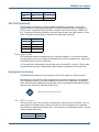
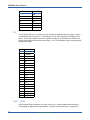
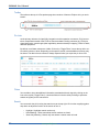
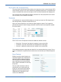
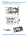
Opal Kelly
XEM6002 User’s Manual
A business-card sized (3.5’’ x 2.0’’) semiconductor
evaluation platform featuring the Xilinx Spartan-6
FPGA and four PmodTM connectors.
The XEM6002 is a small, business-card sized FPGA board featuring the Xilinx Spartan-6 FPGA. Designed as a bare-bones system, the XEM6002 is an excellent platform for semiconductor evaluation and
general experimentation using any of a large number of Pmod devices available from numerous semiconductor manufacturers. The USB 2.0 interface provides fast downloads and easy access with FrontPanel
software. An on-board PLL provides flexible clock generation for a variety of applications and on-board
pushbuttons and LEDs allow simple user interfacing in addition to FrontPanel virtual components. Four
12-pin Pmod connectors are available on two edges of the device.
Software, documentation, samples, and related materials are
Copyright © 2012-2015 Opal Kelly Incorporated.
Opal Kelly Incorporated
Portland, Oregon
http://www.opalkelly.com
All rights reserved. Unauthorized duplication, in whole or part, of this document by any means except for brief
excerpts in published reviews is prohibited without the express written permission of Opal Kelly Incorporated.
Opal Kelly, the Opal Kelly Logo, and FrontPanel are trademarks of Opal Kelly Incorporated.
Linux is a registered trademark of Linus Torvalds. Microsoft and Windows are both registered trademarks of
Microsoft Corporation. All other trademarks referenced herein are the property of their respective owners and no
trademark rights to the same are claimed.
Pmod is a trademark of Digilent, Inc.
Revision History:
Date
Description
20120901
Initial release.
20140331
Added remark about Pins.
20150303
Added additional information about Pins.
Contents
Introducing the XEM6002 . . . . . . . . . . . . . . . . . . . . . . . 5
PCB Footprint. . . . . . . . . . . . . . . . . . . . . . . . . . . . . . . . . . . . . 5
Functional Block Diagram. . . . . . . . . . . . . . . . . . . . . . . . . . . . 6
Power Supply. . . . . . . . . . . . . . . . . . . . . . . . . . . . . . . . . . . . . 6
USB 2.0 Interface. . . . . . . . . . . . . . . . . . . . . . . . . . . . . . . . . . 6
On-board Peripherals. . . . . . . . . . . . . . . . . . . . . . . . . . . . . . . 6
EEPROM . . . . . . . . . . . . . . . . . . . . . . . . . . . . . . . . . . . . . 7
Cypress CY22150 PLL. . . . . . . . . . . . . . . . . . . . . . . . . . . 7
32 Mb SPI Flash [Optional] . . . . . . . . . . . . . . . . . . . . . . . 7
LEDs and Pushbuttons. . . . . . . . . . . . . . . . . . . . . . . . . . . 7
Expansion Connectors. . . . . . . . . . . . . . . . . . . . . . . . . . . . . . 7
FrontPanel Support. . . . . . . . . . . . . . . . . . . . . . . . . . . . . . . . . 7
Programmer’s Interface. . . . . . . . . . . . . . . . . . . . . . . . . . 8
FPGA Pin Connections. . . . . . . . . . . . . . . . . . . . . . . . . 9
Host Interface. . . . . . . . . . . . . . . . . . . . . . . . . . . . . . . . . . . . . 9
MUXSEL. . . . . . . . . . . . . . . . . . . . . . . . . . . . . . . . . . . . . . 9
LEDs and Pushbuttons. . . . . . . . . . . . . . . . . . . . . . . . . . . . . . 10
PLL Connections . . . . . . . . . . . . . . . . . . . . . . . . . . . . . . . . . . 10
SPI Flash [Optional] . . . . . . . . . . . . . . . . . . . . . . . . . . . . . . . . 11
FlashLoader Sample . . . . . . . . . . . . . . . . . . . . . . . . . . . . 11
Expansion Connectors. . . . . . . . . . . . . . . . . . . . . . . . . . . . . . 11
JP4 - JTAG Connector. . . . . . . . . . . . . . . . . . . . . . . . . . . 11
JP1. . . . . . . . . . . . . . . . . . . . . . . . . . . . . . . . . . . . . . . . . . 12
POD1 ... POD4. . . . . . . . . . . . . . . . . . . . . . . . . . . . . . . . . 12
Pins. . . . . . . . . . . . . . . . . . . . . . . . . . . . . . . . . . . . . . . . . . . . . 13
Toolbar. . . . . . . . . . . . . . . . . . . . . . . . . . . . . . . . . . . . . . . 14
Pin Lists . . . . . . . . . . . . . . . . . . . . . . . . . . . . . . . . . . . . . . 14
Filters. . . . . . . . . . . . . . . . . . . . . . . . . . . . . . . . . . . . . . . . 14
Search . . . . . . . . . . . . . . . . . . . . . . . . . . . . . . . . . . . . . . . 14
Export (PDF, CSV, Constraints Files). . . . . . . . . . . . . . . . 15
Peripherals. . . . . . . . . . . . . . . . . . . . . . . . . . . . . . . . . . . . 15
XEM6002 Mechanical Drawing. . . . . . . . . . . . . . . . . . . 16
XEM6002 User’s Manual
4
www.opalkelly.com
XEM6002 User’s Manual
Introducing the XEM6002
The XEM6002 is a small, business-card sized (3.5’’ x 2.0’’) FPGA board featuring the Xilinx
Spartan-6 FPGA. Combined with the powerful FrontPanel SDK and easy-to-use FrontPanel
Application, the XEM6002 is an excellent platform for semiconductor evaluation and experimentation. Featuring four Pmod connectors, the XEM6002 can interface to hundreds of peripheral
modules available from several semiconductor manufacturers
PCB Footprint
A mechanical drawing of the XEM6002 is provided at the end of this document. The PCB is
3.5” x 2.0” (88.9mm x 50.8mm) with four mounting holes spaced as shown in the figure. These
mounting holes are electrically isolated (disconnected).
The five FPGA-access ports POD1...POD4 and JP1 are arranged on three edges of the device.
A JTAG header (JP4) is also provided.
www.opalkelly.com
5
XEM6002 User’s Manual
Functional Block Diagram
POD1
8 I/O
17 I/O
Host Interface
Bus
PLL
(CY22150)
8 I/O
Spartan-6 FPGA
(XC6SLX9-2FTG256C)
3 PLL CLKs
(3 GCLK)
(1 PLL CLK)
ZBUS (JP1)
USB Micro
(CY68013A)
USB
POD2
12 I/O
4 Pushbuttons
8 I/O
POD3
8 I/O
8 LEDs
POD4
Power Supply
The XEM6002 is a bus-powered device. That is, it takes power from the 5-v USB power and
generates the voltages it needs from there. To do so, the XEM6002 has small linear regulators
for 3.3v, and 1.2v.
Computers and USB hubs often have USB ports that do not provide bus power. These are called
unpowered ports. In order to be operated as a bus-powered device, the XEM6002 must be
connected to a USB port that provides bus power. You should check with the hub or computer
manufacturer to verify that the port provides bus power.
IMPORTANT NOTE: Under normal operating conditions and with an unconfigured FPGA, the XEM6002 draws approximately 125 mA from the 3.3-V node.
FPGA current draw is impossible to predict because it strongly depends on the
implemented design, clock rates, and I/O usage. Current requirements of the
FPGA can be estimated using Xilinx power estimation tools and should be considered if you think you may be getting close to USB limits.
USB 2.0 Interface
The XEM6002 uses a Cypress CY7C68013A FX2 USB microcontroller to make the device a
USB 2.0 peripheral. As a USB peripheral, the module is instantly recognized as a plug and play
peripheral on millions of PCs. More importantly, FPGA downloads happen blazingly fast, virtual
instruments under FrontPanel update quickly, and data transfers are much faster than the parallel
port interfaces common on many FPGA experimentation boards.
The USB interface also allows the XEM to be bus-powered which means it is ultra-portable
requiring just a USB cable and the proper drivers to connect to any supporting PC, including
laptops.
On-board Peripherals
The XEM6002 is designed as a low-cost, barebones device. However, a few key peripherals
have been added for convenience.
6
www.opalkelly.com
XEM6002 User’s Manual
EEPROM
A small serial EEPROM is attached to the USB microcontroller on the XEM6002, but not directly
available to the FPGA. The EEPROM is used to store boot code for the microcontroller as well
as PLL configuration data and a device identifier string.
The PLL configuration data is loaded from EEPROM and used to reconfigure the PLL each time
a new configuration file is loaded to the FPGA. Therefore, stable and active clocks will be present on the FPGA pins as soon as it comes out of configuration. The stored PLL configuration
may be changed at any time using FrontPanel’s PLL Configuration Dialog.
The EEPROM also stores a device identifier string which may be changed at any time using
FrontPanel. The string serves only a cosmetic purpose and is used when multiple XEM devices
are attached to the same computer so you may select the proper active device.
Cypress CY22150 PLL
A multi-output, single-VCO PLL can provide up to five clocks, three to the FPGA and another two
to the expansion connectors JP2 and JP3. The PLL is driven by a 48-MHz signal output from the
USB microcontroller. The PLL can output clocks up to 150-MHz and is configured through the
FrontPanel software interface or the FrontPanel API.
32 Mb SPI Flash [Optional]
Note: The SPI Flash is an OEM option and is not available in the default configuration.
A serial flash device is available to the FPGA for configuration booting and post-configuration usage as general-purpose non-volatile memory.
LEDs and Pushbuttons
Eight LEDs and four pushbuttons are available for general use as debug inputs and outputs.
Expansion Connectors
Four Pmod connectors are available to interface with external devices. The I/O signals on these
connectors are wired through series resistors to the FPGA I/Os. ESD protection diodes are also
connected at the connector pin.
One 0.1”-spaced expansion connector (JP1) is also provided for external connection. This connector provides 3.3v power, ground, one PLL output, and 17 FPGA pins for general I/O.
NOTE: The expansion connectors are not installed at the factory to provide you
the flexibility of installing your choice of expansion -- directly soldering wires, or
using stacking or right-angle connectors.
FrontPanel Support
The XEM6002 is fully supported by the Opal Kelly FrontPanel Application. FrontPanel augments
the limited peripheral support with a host of PC-based virtual instruments such as LEDs, hex
displays, pushbuttons, toggle buttons, and so on. Essentially, this makes your PC a reconfigurable I/O board and adds enormous value to the XEM6002 as an experimentation or prototyping
system.
www.opalkelly.com
7
XEM6002 User’s Manual
Programmer’s Interface
In addition to complete support within FrontPanel, the XEM6002 is also fully-supported by the
FrontPanel software development kit (SDK), a powerful API library available to Windows, Mac
OS X, and Linux programmers allowing you to easily interface your own software to the XEM.
In addition to the C++ library, wrappers have been written for Java and Python making the API
available under those languages as well. Java and Python extensions are available under Windows, Mac OS X, and Linux.
Complete documentation and several sample programs are installed with FrontPanel.
8
www.opalkelly.com
XEM6002 User’s Manual
FPGA Pin Connections
Host Interface
There are 27 pins that connect the on-board USB microcontroller to the FPGA. These pins comprise the host interface on the FPGA and are used for configuration downloads. After configuration, these pins are used to allow FrontPanel communication with the FPGA.
If the FrontPanel okHostInterface module is instantiated in your design, you must map the interface pins to specific pin locations using Xilinx LOC constraints. This may be done using the
Xilinx constraints editor or specifying the constraints manually in a text file.
A template constraints file (xem6002.ucf) is located in the Samples directory of the FrontPanel
installation. This file lists all the XEM6002 pins and maps them to the appropriate FPGA pins using LOC (location) constraints. You can use this template to quickly get the pin locations correct
on a new design.
MUXSEL
MUXSEL is a signal on the XEM6002 which selects the signal path to the FPGA programming
signals D0 and CCLK. When low (deasserted), the FPGA and USB microcontroller are connected. When high (asserted), the FPGA and Flash are connected.
In normal USB-programmed operation, JP5 is positioned at “USB” and pulls MUXSEL low, connecting the FPGA and USB microcontroller at all times. This allows USB-based programming of
the FPGA and subsequent USB communication with the FPGA design after configuration.
In order to allow the Flash to configure the FPGA, JP5 is positioned at “PROM.” In order to deassert MUXSEL post-configuration, your design must deassert MUXSEL. This allows the FPGA
www.opalkelly.com
9
XEM6002 User’s Manual
design to properly startup and allows for communication over USB even after the Flash has configured it.
The end result is that your FPGA design should always tie HI_MUXSEL to 0. This is the case
regardless of how the design was configured (via Flash or USB). For example, in Verilog:
assign hi_muxsel = 1’b0;
Note: MUXSEL handling is only required on XEM6002 which have the SPI Flash inserted (an
OEM option). However, no harm is done including the above HDL in all designs. Therefore, we
recommend including this as a general rule.
LEDs and Pushbuttons
There are eight LEDs and four pushbuttons on the XEM6002. Each is wired directly to the FPGA
as shown in the tables below.
LED
FPGA Pin
Button
FPGA Pin
D1
K2
BTN1
C5
D2
N3
BTN2
A4
D3
R2
BTN3
C8
D4
R1
BTN4
A9
D5
P2
D6
P1
D7
N1
D8
M2
The LED anodes are connected to a pull-up resistor to +3.3VDD and the cathodes wired directly
to the FPGA. To turn ON an LED, the FPGA pin should be brought low. To turn OFF an LED,
the FPGA pin should be brought high.
The pushbuttons are connected between their respective FPGA pin and DGND. The FPGA side
of the connection has a pull-up resistor to +3.3VDD. Therefore, in the pressed state, the FPGA
pin will be at DGND (low) and in the unpressed state, the FPGA pin will be at +3.3VDD (high).
Note that the pushbuttons are not debounced on the XEM6002. In order to deglitch the signals
from the pushbuttons, proper debouncing should be done inside the FPGA.
PLL Connections
The PLL contains six output pins, two of which are unconnected. The other four are labelled
SYS_CLK1 through SYS_CLK4. SYS_CLK4 connects to JP1. The other three pins are connected directly to the FPGA. The table below illustrates the PLL connections.
10
PLL Pin
Clock Name
Connection
LCLK1
SYS_CLK1
FPGA - T8
LCLK2
SYS_CLK2
FPGA - K12
LCLK3
SYS_CLK3
FPGA - H4
LCLK4
SYS_CLK4
JP1 - Pin 1
www.opalkelly.com
XEM6002 User’s Manual
PLL Pin
Clock Name
CLK5
N/A
CLK6
N/A
Connection
SPI Flash [Optional]
The SPI flash on the module is a Numonyx M25P32-VME6G or equivalent. It can be programmed (using the FlashLoader sample) with an FPGA configuration bitfile to configure the
FPGA on boot. To boot the FPGA from flash, the switch JP5 must be slid to the “PROM” position. To boot the FPGA using FrontPanel, the switch must be slid to the “USB” position. In both
cases, FrontPanel communication is available after configuration completes.
Flash Pin
FPGA Pin
C
M9
S
T3
D
R9
Q
T9
FlashLoader Sample
The FlashLoader sample is installed with your FrontPanel installation. It is a simple commandline utility that you can use to program the SPI flash with an FPGA configuration file. Please see
the Samples directory for more information.
You can also load a configuration file to the Flash using your own HDL, of course. There is nothing special about the way our FlashLoader sample loads the configuration file into the Flash.
Expansion Connectors
The XEM6002 has locations for five expansion connectors in addition to a JTAG connector.
Opal Kelly Pins is an interactive online reference for the expansion connectors on all Opal Kelly
FPGA integration modules. It provides additional information on pin capabilities, pin characteristics, and PCB routing. Additionally, Pins provides a tool for generating constraint files for place
and route tools. Pins can be found at the URL below.
http://www.opalkelly.com/pins
JP4 - JTAG Connector
JP4 is the 14-pin 2-mm JTAG connector on-board and is connected only to the FPGA. The connector pinout is compatible with the Xilinx JTAG cable for JTAG configuration and ChipScope.
The JP4 pins are connected as shown below. This connector is not installed by default. The part
number is Molex 87831-1420.
JP4 Pin
Signal
2
+3.3VDD
www.opalkelly.com
11
XEM6002 User’s Manual
JP4 Pin
Signal
4
TMS
6
TCK
8
TDO
10
TDI
12
NC
14
NC
1,3,5,7,9, 11,13
DGND
JP1
JP1 is a 20-pin dual-row 0.1” header, two pins of which are dedicated to power supply. One pin
is connected to the on-board PLL. The remaining 17 pins connect directly to the Spartan-6 on
bank 0. Pin 19 of the header connects to a global clock pin on the FPGA and can therefore be
used as clock inputs to the internal clock network. All 17 FPGA signals may be used as generalpurpose input/output.
JP1
Connection
1
SYS_CLK4
2
+3.3VDD
3
B5
4
A5
5
B6
6
A6
7
C6
8
A7
9
A8
10
B8
11
A10
12
B10
13
A11
14
A12
15
A13
16
B12
17
A14
18
C13
19
E8 (GCLK)
20
DGND
POD1 ... POD4
POD1 through POD4 connectors are 12-pin, dual-row, 0.1” female headers which have a pinout satisfying the Digilent Pmod specification. Two pins of each connector are connected to
12
www.opalkelly.com
XEM6002 User’s Manual
+3.3VDD and two pins are connected to DGND. The remaining 8 pins are connected to the
FPGA on banks 1 and 3.
POD1
Signal
POD2
Signal
1
M1
1
A2
2
L1
2
B2
3
K1
3
B3
4
J1
4
A3
5
DGND
5
DGND
6
+3.3VDD
6
+3.3VDD
7
E1
7
B1
8
E2
8
C2
9
F1
9
C1
10
G1
10
D1
11
DGND
11
DGND
12
+3.3VDD
12
+3.3VDD
POD3
Signal
POD4
Signal
1
F15
1
B15
2
G16
2
B16
3
J16
3
C15
4
L16
4
C16
5
DGND
5
DGND
6
+3.3VDD
6
+3.3VDD
7
F16
7
E16
8
H16
8
E15
9
K16
9
D16
10
M16
10
D14
11
DGND
11
DGND
12
+3.3VDD
12
+3.3VDD
Pins
Opal Kelly Pins is an interactive online reference for the expansion connectors on all Opal Kelly
FPGA integration modules. It provides additional information on pin capabilities, pin characteristics, and PCB routing. Additionally, Pins provides a tool for generating constraint files for place
and route tools. Pins can be found at the URL below.
http://www.opalkelly.com/pins
www.opalkelly.com
13
XEM6002 User’s Manual
Toolbar
The toolbar at the top of a Pins product page has a number of features. Explore a bit; you won’t
break it.
Pin Lists
As the primary reference for Opal Kelly integration module expansion connectors, Pin Lists contain a comprehensive table of the FPGA-to-Connector data including connector pin, FPGA pin,
signal description, routed length (when applicable), breakout board pin mapping, FPGA I/O bank,
and other properties.
By default, not all data columns are visible. Click on the “Toggle Filters” icon at the top-left to select which columns to show. Depending on the specific module, several additional columns may
be shown. The data in these columns is always exported when you export the pin list to CSV.
Filters
You can hide or show the additional information associated with each signal by clicking on the
icon at the top left (“Toggle Filters”). Use these filters to limit the visible pin listing to particular
subsets of signals you are interested in.
Search
You can search the pin list using the search entry at the top-right. Click on the magnifying glass
drop-down to adjust the function of the search to one of:
•
•
•
14
Highlight - Highlights search results only.
Hide Matching - Hides rows where search matches are found.
Show Only Matching - Shows only rows where a search match is found.
www.opalkelly.com
XEM6002 User’s Manual
Export (PDF, CSV, Constraints Files)
The export button near the search entry allows you to export the pin list in several formats. PDFs
can be viewed or printed. CSV can be loaded into a spreadsheet application or manipulated with
scripts. Constraints files can be used as inputs to Xilinx and Altera synthesis and mapping tools.
The constraints files include additional mapping information for other peripherals on the module
such as memory, clock oscillators, and LEDs.
Peripherals
A Pins Peripheral is a project definition where you can enter your top-level HDL design nets to
have Pins generate a complete constraint file for you.
When you create a Peripheral, you will select a target integration module. The Peripheral is
paired to this module so that the design parameters match the features and expansion capabilities of the module.
Specifying Net Names
The Pin List view for a Peripheral includes three additional, editable columns:
•
•
•
Design Net - The name of the signal as it appears in your top-level HDL.
Constraints - Text that is inserted into the constraints file for that signal.
Comment - Additional comment text that is added to the constraints file.
These additional data are merged with the default Pin List constraints file prior to export. The result is a constraints file complete with net names that can be used with your FPGA development
flow.
Export Features
Enable the specific module features you
would like to appear in the exported constraints file. When a feature is enabled,
Pins will export the constraints appropriate to that feature such as pin locations.
When a feature is disabled, Pins will skip
that portion.
The User Lead In and User Lead Out
sections allow you to add custom payloads (your own constraints) that will be
added to the exported constraints file.
Additional timing constraints or comments can be added here.
www.opalkelly.com
15
XEM6002 User’s Manual
XEM6002 Mechanical Drawing
00
3.
50.80
46.99
29.89
22.19
80.26
85.09
88.90
64.52
57.40
41.66
0
3.81
3.81
0
50.80
7.70
38.10
36.83
12.70
7.35
6.62
5.65
0
All dimensions in mm
16
www.opalkelly.com
88.90
60.04
45.72
33.02
22.86
0
5.08
10.16
0