1
CFD-ACE+ 2003 : Integrated Circuit (IC) Thermal Analysis Tutorial
____________________________________________________________________________________
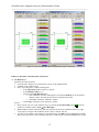
rectangle are appropriate. If not, correct them by typing the accurate number (Pos.X = 0, Pos.Y = 0, Size X
= 100, Size Y = 100), and click Accept.
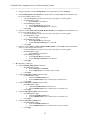
11. Edit Bulk_Silicon layer:
Operation and vertical position:
• Click LB on the “Bulk_Silicon” layer from the list of layers on the right-hand side
• Click RB on the “Bulk_Silicon” layer
• In the “Layer Properties” window which appears:
o set the Operation: pull-down menu to “deposit”
o set the Thickness [um]: to 0.5
o click Accept
Layout:
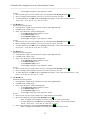
• Draw a layout (top view) of the “Bulk_Silicon” layer, by selecting the New Rectangle button [ ]
• Draw a rectangle with coordinates (0 um, 0 um) to (100 um, 100 um).
• To check dimensions, click RB on the red (highlighted) rectangle: correct values should be (Pos.X = 0,
Pos.Y = 0, Size X = 100, Size Y = 100)
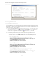
12. Edit Oxide layer:
Operation and vertical position:
• Click LB on the “Oxide” layer from the list of layers on the right-hand side
• Click RB on the “Oxide” layer
• In the “Layer Properties” window which appears:
o set the Operation: pull-down menu to “deposit”
o set the Thickness [um]: to 4.5
o click Accept, closing the “Layer Properties” window
Layout:
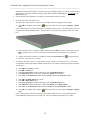
• Draw a layout (top view) of the “Oxide” layer, by selecting the New Rectangle button [ ]
• Draw a rectangle with coordinates (0 um, 0 um) to (100 um, 100 um).
• To check dimensions, click RB on the red (highlighted) rectangle: correct values should be (Pos.X = 0,
Pos.Y = 0, Size X = 100, Size Y = 100)
13. Edit Semi_Device layer:
Operation and vertical position:
• Click LB on the “Semi_Device” layer from the list of layers on the right-hand side
• Click RB on the “Semi_Device” layer
• In the “Layer Properties” window which appears:
o set the Operation: pull-down menu to “insert”
o set the Position [um]: to 0.7
o set the Thickness [um]: to 0.05
o click Accept, closing the “Layer Properties” window
Layout:
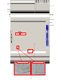
• Draw a layout (top view) of the “Semi_Device” layer, by selecting the New Rectangle button [ ]
• Draw a rectangle with coordinates (22.24 um, 22.4 um) to (85.92 um, 64 um).
• To check dimensions, click RB on the red (highlighted) rectangle: correct values should be (Pos.X =
22.24, Pos.Y = 22.4, Size X = 63.68, Size Y = 41.6)
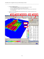
14. Edit HeatA layer:
Operation and vertical position:
• Click LB on the “HeatA” layer from the list of layers on the right-hand side
• Click RB on the “HeatA” layer
• In the “Layer Properties” window which appears:
o set the Operation: pull-down menu to “insert”
o set the Position [um]: to 0.75
o set the Thickness [um]: to 0.15
14