1
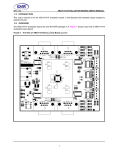
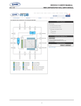
XR20M1170 EVALUATION BOARD USER’S MANUAL
REV. 1.0.0
INTRODUCTION
This user’s manual is for the XR20M1170 evaluation board. Table 1 shows the different devices and packages
that the evaluation board support. This user’s manual will describe the hardware setup required to operate the
different packages.
1.0 HARDWARE SETUP
1.1
Packages description
Since the XR20M1170 evaluation board can be used for both the XR20M1170 and XR20V2170, Table 1 shows
the different packages supported by the board.
TABLE 1: PACKAGE LIST
1.2
PART NUMBER
PACKAGE
LOCATION
XR20M1170IL28
28-pin QFN
U6
XR20M1170IL24
24-pin QFN
U2
XR20M1170IL16
16-pin QFN
U5
XR20M1170IG24
24-pin TSSOP
U9
XR20M1170IG16
16-pin TSSOP
U8
XR20V2170IL40
40-pin QFN
U4
Jumper Settings
1.2.1
XR20M1170IL28
The following jumpers apply to the XR20M1170IL28:
TABLE 2: JUMPER SETTINGS FOR XR20M1170IL28
JUMPERS
J25
FUNCTIONS
COMMENTS
Jumper in selects SPI mode
Selects between I2C and SPI mode
Jumper out selects I2C mode
J5
Power for the RS-232 Transceiver
Jumper in enables power for RS-232 Transceiver
Jumper out disables power for RS-232 Transceiver
J11
Routing of modem signals to RS-232 Transceiver
Jumper not installed
Trace between 1&2
Trace between 3&4
Trace between 5&6
Trace between 7&8
J7
For internal test only
J4
For internal test only
Not installed
J29
I2C Address Select (A0)
■ 1&2 = VCC
■ 3&4 = SCL
■ 5&6 = SDA
■ 7&8 = GND
For I2C mode, only one jumper should be selected.
See XR20M1170 datasheet for I2C addressing.
For SPI mode, jumper should be out.
1
XR20M1170 EVALUATION BOARD USER’S MANUAL
REV. 1.0.0
TABLE 2: JUMPER SETTINGS FOR XR20M1170IL28
JUMPERS
FUNCTIONS
COMMENTS
J30
I2C Address Select (A1)
■ 1&2 = VCC
■ 3&4 = SCL
■ 5&6 = SDA
■ 7&8 = GND
For I2C mode, only one jumper should be selected.
See XR20M1170 datasheet for I2C addressing.
For SPI mode, jumper should be out.
J13
Header for connection to external microcontroller
board
Ground and Power connections
■
■
■
■
■
■
■
■
■
Pin 2 = SDA signal for I2C interface
Pin 3 = SO signal for SPI interface
Pin 4 = IRQ# output signal from XR20M1170
■
■
Pin 17 should be connected to GND
Pin 18 should be connected +3.3V
If I2C interface is used:
Pin 13 = A0 signal for
interface or CS# for
■ Pin 2 should be connected to SDA
SPI interface
■ Pin 4 should be connected to MCU interrupt
input (if using interrupts)
Pin 14 = A1 signal for I2C interface or SI for
SPI interface
■ Pin 13 should be unconnected when using J29
Pin 15 = RESET# input signal
■ Pin 14 should be unconnected when using J30
2
■ Pin 15 should be connected to reset output from
Pin 16 = SCL signal for I C interface or SCK
MCU
for SPI interface
■
Pin 16 should be connected to SCL
Pin 17 = GND signal
I2C
Pin 18 = External power for XR20M1170 and If SPI interface is used:
RS-232 Transceiver
■ Pin 2 should be unconnected
■ Pin 3 should be connected to SO
■ Pin 4 should be connected to MCU interrupt (if
using interrupts)
■ Pin 13 should be connected to CS#
■ Pin 14 should be connected to SI
■ Pin 15 should be connected to reset output from
MCU
■ Pin 16 should be connected to SCK
J16
Power supply for the XR20M1170IL28
Jumper not installed
Trace between 1&2
J17
Enable/Disable RS-485 feature
Jumper in enables RS-485 mode
Jumper out disables RS-485 mode
J18
Enable/Disable IR feature
Jumper in enables IR mode
Jumper out disables IR mode
J26
Enable/Disable UART side external loopback
Jumper in enables UART side external loopback
Jumper out disables UART side external loopback
2
XR20M1170 EVALUATION BOARD USER’S MANUAL
REV. 1.0.0
1.2.2
XR20M1170IL24
The following jumpers apply to the XR20M1170IL24:
TABLE 3: JUMPER SETTINGS FOR XR20M1170IL24
JUMPERS
J25
FUNCTIONS
COMMENTS
Jumper in selects SPI mode
Selects between I2C and SPI mode
Jumper out selects I2C mode
J5
Power for the RS-232 Transceiver
Jumper in enables power for RS-232 Transceiver
Jumper out disables power for RS-232 Transceiver
J11
Routing of modem signals to RS-232 Transceiver
Jumper not installed
Trace between 1&2
Trace between 3&4
Trace between 5&6
Trace between 7&8
J7
For internal test only
J4
For internal test only
Not installed
J29
I2C Address Select (A0)
■ 1&2 = VCC
■ 3&4 = SCL
■ 5&6 = SDA
■ 7&8 = GND
For I2C mode, only one jumper should be selected.
See XR20M1170 datasheet for I2C addressing.
For SPI mode, jumper should be out.
J30
I2C Address Select (A1)
■ 1&2 = VCC
■ 3&4 = SCL
■ 5&6 = SDA
■ 7&8 = GND
For I2C mode, only one jumper should be selected.
See XR20M1170 datasheet for I2C addressing.
For SPI mode, jumper should be out.
3
XR20M1170 EVALUATION BOARD USER’S MANUAL
REV. 1.0.0
TABLE 3: JUMPER SETTINGS FOR XR20M1170IL24
JUMPERS
J13
FUNCTIONS
Header for connection to external microcontroller
board
■
■
■
■
■
■
■
■
■
J8
COMMENTS
Pin 2 = SDA signal for I2C interface
Pin 3 = SO signal for SPI interface
Pin 4 = IRQ# output signal from XR20M1170
Ground and Power connections
■
■
Pin 17 should be connected to GND
Pin 18 should be connected +3.3V
If I2C interface is used:
Pin 13 = A0 signal for
interface or CS# for
■ Pin 2 should be connected to SDA
SPI interface
■ Pin 4 should be connected to MCU interrupt
2
input (if using interrupts)
Pin 14 = A1 signal for I C interface or SI for
SPI interface
■ Pin 13 should be unconnected when using J29
Pin 15 = RESET# input signal
■ Pin 14 should be unconnected when using J30
■ Pin 15 should be connected to reset output from
Pin 16 = SCL signal for I2C interface or SCK
MCU
for SPI interface
■ Pin 16 should be connected to SCL
Pin 17 = GND signal
I2C
Pin 18 = External power for XR20M1170 and If SPI interface is used:
RS-232 Transceiver
■ Pin 2 should be unconnected
■ Pin 3 should be connected to SO
■ Pin 4 should be connected to MCU interrupt (if
using interrupts)
■ Pin 13 should be connected to CS#
■ Pin 14 should be connected to SI
■ Pin 15 should be connected to reset output from
MCU
■ Pin 16 should be connected to SCK
Power supply for the XR20M1170IL24
Jumper not installed
Trace between 1&2
4
XR20M1170 EVALUATION BOARD USER’S MANUAL
REV. 1.0.0
1.2.3
XR20M1170IG24
The following jumpers apply to the XR20M1170IG24:
TABLE 4: JUMPER SETTINGS FOR XR20M1170IG24
JUMPERS
J25
FUNCTIONS
COMMENTS
Jumper in selects SPI mode
Selects between I2C and SPI mode
Jumper out selects I2C mode
J5
Power for the RS-232 Transceiver
Jumper in enables power for RS-232 Transceiver
Jumper out disables power for RS-232 Transceiver
J11
Routing of modem signals to RS-232 Transceiver
Jumper not installed
Trace between 1&2
Trace between 3&4
Trace between 5&6
Trace between 7&8
J7
For internal test only
J4
For internal test only
Not installed
J29
I2C Address Select (A0)
■ 1&2 = VCC
■ 3&4 = SCL
■ 5&6 = SDA
■ 7&8 = GND
For I2C mode, only one jumper should be selected.
See XR20M1170 datasheet for I2C addressing.
For SPI mode, jumper should be out.
J30
I2C Address Select (A1)
■ 1&2 = VCC
■ 3&4 = SCL
■ 5&6 = SDA
■ 7&8 = GND
For I2C mode, only one jumper should be selected.
See XR20M1170 datasheet for I2C addressing.
For SPI mode, jumper should be out.
5
XR20M1170 EVALUATION BOARD USER’S MANUAL
REV. 1.0.0
TABLE 4: JUMPER SETTINGS FOR XR20M1170IG24
JUMPERS
J13
FUNCTIONS
Header for connection to external microcontroller
board
■
■
■
■
■
■
■
■
■
J23
COMMENTS
Pin 2 = SDA signal for I2C interface
Pin 3 = SO signal for SPI interface
Pin 4 = IRQ# output signal from XR20M1170
Ground and Power connections
■
■
Pin 17 should be connected to GND
Pin 18 should be connected +3.3V
If I2C interface is used:
Pin 13 = A0 signal for
interface or CS# for
■ Pin 2 should be connected to SDA
SPI interface
■ Pin 4 should be connected to MCU interrupt
2
input (if using interrupts)
Pin 14 = A1 signal for I C interface or SI for
SPI interface
■ Pin 13 should be unconnected when using J29
Pin 15 = RESET# input signal
■ Pin 14 should be unconnected when using J30
■ Pin 15 should be connected to reset output from
Pin 16 = SCL signal for I2C interface or SCK
MCU
for SPI interface
■ Pin 16 should be connected to SCL
Pin 17 = GND signal
I2C
Pin 18 = External power for XR20M1170 and If SPI interface is used:
RS-232 Transceiver
■ Pin 2 should be unconnected
■ Pin 3 should be connected to SO
■ Pin 4 should be connected to MCU interrupt (if
using interrupts)
■ Pin 13 should be connected to CS#
■ Pin 14 should be connected to SI
■ Pin 15 should be connected to reset output from
MCU
■ Pin 16 should be connected to SCK
Power supply for the XR20M1170IG24
Jumper not installed
Trace between 1&2
6
XR20M1170 EVALUATION BOARD USER’S MANUAL
REV. 1.0.0
1.2.4
XR20M1170IL16
The following jumpers apply to the XR20M1170IL16:
TABLE 5: JUMPER SETTINGS FOR XR20M1170IL16 PACKAGE
JUMPERS
J25
FUNCTIONS
COMMENTS
Jumper in selects SPI mode
Selects between I2C and SPI mode
Jumper out selects I2C mode
J5
Power for the RS-232 Transceiver
Jumper in enables power for RS-232 Transceiver
Jumper out disables power for RS-232 Transceiver
J11
Routing of modem signals to RS-232 Transceiver
Jumper not installed
Trace between 1&2
Trace between 3&4
Trace between 5&6
Trace between 7&8
J7
For internal test only
J4
For internal test only
Not installed
J29
I2C Address Select (A0)
■ 1&2 = VCC
■ 3&4 = SCL
■ 5&6 = SDA
■ 7&8 = GND
For I2C mode, only one jumper should be selected.
See XR20M1170 datasheet for I2C addressing.
For SPI mode, jumper should be out.
J30
I2C Address Select (A1)
■ 1&2 = VCC
■ 3&4 = SCL
■ 5&6 = SDA
■ 7&8 = GND
For I2C mode, only one jumper should be selected.
See XR20M1170 datasheet for I2C addressing.
For SPI mode, jumper should be out.
7
XR20M1170 EVALUATION BOARD USER’S MANUAL
REV. 1.0.0
TABLE 5: JUMPER SETTINGS FOR XR20M1170IL16 PACKAGE
JUMPERS
J13
FUNCTIONS
Header for connection to external microcontroller
board
■
■
■
■
■
■
■
■
■
J15
COMMENTS
Pin 2 = SDA signal for I2C interface
Pin 3 = SO signal for SPI interface
Pin 4 = IRQ# output signal from XR20M1170
Ground and Power connections
■
■
Pin 17 should be connected to GND
Pin 18 should be connected +3.3V
If I2C interface is used:
Pin 13 = A0 signal for
interface or CS# for
■ Pin 2 should be connected to SDA
SPI interface
■ Pin 4 should be connected to MCU interrupt
2
input (if using interrupts)
Pin 14 = A1 signal for I C interface or SI for
SPI interface
■ Pin 13 should be unconnected when using J29
Pin 15 = RESET# input signal
■ Pin 14 should be unconnected when using J30
■ Pin 15 should be connected to reset output from
Pin 16 = SCL signal for I2C interface or SCK
MCU
for SPI interface
■ Pin 16 should be connected to SCL
Pin 17 = GND signal
I2C
Pin 18 = External power for XR20M1170 and If SPI interface is used:
RS-232 Transceiver
■ Pin 2 should be unconnected
■ Pin 3 should be connected to SO
■ Pin 4 should be connected to MCU interrupt (if
using interrupts)
■ Pin 13 should be connected to CS#
■ Pin 14 should be connected to SI
■ Pin 15 should be connected to reset output from
MCU
■ Pin 16 should be connected to SCK
Power supply for the XR20M1170IL16
Jumper not installed
Trace between 1&2
8
XR20M1170 EVALUATION BOARD USER’S MANUAL
REV. 1.0.0
1.2.5
XR20M1170IG16
The following jumpers apply to the XR20M1170IG16:
TABLE 6: JUMPER SETTINGS FOR XR20M1170IG16
JUMPERS
J25
FUNCTIONS
COMMENTS
Jumper in selects SPI mode
Selects between I2C and SPI mode
Jumper out selects I2C mode
J5
Power for the RS-232 Transceiver
Jumper in enables power for RS-232 Transceiver
Jumper out disables power for RS-232 Transceiver
J11
Routing of modem signals to RS-232 Transceiver
Jumper not installed
Trace between 1&2
Trace between 3&4
Trace between 5&6
Trace between 7&8
J7
For internal test only
J4
For internal test only
Not installed
J29
I2C Address Select (A0)
■ 1&2 = VCC
■ 3&4 = SCL
■ 5&6 = SDA
■ 7&8 = GND
For I2C mode, only one jumper should be selected.
See XR20M1170 datasheet for I2C addressing.
For SPI mode, jumper should be out.
J30
I2C Address Select (A1)
■ 1&2 = VCC
■ 3&4 = SCL
■ 5&6 = SDA
■ 7&8 = GND
For I2C mode, only one jumper should be selected.
See XR20M1170 datasheet for I2C addressing.
For SPI mode, jumper should be out.
9
XR20M1170 EVALUATION BOARD USER’S MANUAL
REV. 1.0.0
TABLE 6: JUMPER SETTINGS FOR XR20M1170IG16
JUMPERS
J13
FUNCTIONS
Header for connection to external microcontroller
board
■
■
■
■
■
■
■
■
■
J22
COMMENTS
Pin 2 = SDA signal for I2C interface
Pin 3 = SO signal for SPI interface
Pin 4 = IRQ# output signal from XR20M1170
Ground and Power connections
■
■
Pin 17 should be connected to GND
Pin 18 should be connected +3.3V
If I2C interface is used:
Pin 13 = A0 signal for
interface or CS# for
■ Pin 2 should be connected to SDA
SPI interface
■ Pin 4 should be connected to MCU interrupt
2
input (if using interrupts)
Pin 14 = A1 signal for I C interface or SI for
SPI interface
■ Pin 13 should be unconnected when using J29
Pin 15 = RESET# input signal
■ Pin 14 should be unconnected when using J30
■ Pin 15 should be connected to reset output from
Pin 16 = SCL signal for I2C interface or SCK
MCU
for SPI interface
■ Pin 16 should be connected to SCL
Pin 17 = GND signal
I2C
Pin 18 = External power for XR20M1170 and If SPI interface is used:
RS-232 Transceiver
■ Pin 2 should be unconnected
■ Pin 3 should be connected to SO
■ Pin 4 should be connected to MCU interrupt (if
using interrupts)
■ Pin 13 should be connected to CS#
■ Pin 14 should be connected to SI
■ Pin 15 should be connected to reset output from
MCU
■ Pin 16 should be connected to SCK
Power supply for the XR20M1170IG16
Jumper not installed
Trace between 1&2
10
XR20M1170 EVALUATION BOARD USER’S MANUAL
REV. 1.0.0
1.2.6
XR20V2170IL40
The following jumpers apply to the XR20V2170IL40:
TABLE 7: JUMPER SETTINGS FOR XR20V2170IL40
JUMPERS
J25
FUNCTIONS
COMMENTS
Jumper in selects SPI mode
Selects between I2C and SPI mode
Jumper out selects I2C mode
J5
Power for the RS-232 Transceiver
Jumper in enables power for RS-232 Transceiver
Jumper out disables power for RS-232 Transceiver
J11
Routing of modem signals to RS-232 Transceiver
Jumper not installed
Trace between 1&2
Trace between 3&4
Trace between 5&6
Trace between 7&8
J7
For internal test only
J4
For internal test only
Not installed
J29
I2C Address Select (A0)
■ 1&2 = VCC
■ 3&4 = SCL
■ 5&6 = SDA
■ 7&8 = GND
For I2C mode, only one jumper should be selected.
See XR20V2170 datasheet for I2C addressing.
For SPI mode, jumper should be out.
J30
I2C Address Select (A1)
■ 1&2 = VCC
■ 3&4 = SCL
■ 5&6 = SDA
■ 7&8 = GND
For I2C mode, only one jumper should be selected.
See XR20V2170 datasheet for I2C addressing.
For SPI mode, jumper should be out.
11
XR20M1170 EVALUATION BOARD USER’S MANUAL
REV. 1.0.0
TABLE 7: JUMPER SETTINGS FOR XR20V2170IL40
JUMPERS
J13
FUNCTIONS
COMMENTS
Header for connection to external microcontroller
board
■
■
■
■
■
■
■
■
■
Ground and Power connections
■
Pin 2 = SDA signal for I2C interface
Pin 3 = SO signal for SPI interface
Pin 4 = IRQ# output signal from XR20M1170
■
Pin 17 should be connected to GND
Pin 18 should be connected +3.3V
If I2C interface is used:
Pin 13 = A0 signal for
interface or CS# for
■ Pin 2 should be connected to SDA
SPI interface
■ Pin 4 should be connected to MCU interrupt
2
input (if using interrupts)
Pin 14 = A1 signal for I C interface or SI for
SPI interface
■ Pin 13 should be unconnected when using J29
Pin 15 = RESET# input signal
■ Pin 14 should be unconnected when using J30
■ Pin 15 should be connected to reset output from
Pin 16 = SCL signal for I2C interface or SCK
MCU
for SPI interface
■ Pin 16 should be connected to SCL
Pin 17 = GND signal
I2C
Pin 18 = External power for XR20M1170 and If SPI interface is used:
RS-232 Transceiver
■ Pin 2 should be unconnected
■ Pin 3 should be connected to SO
■ Pin 4 should be connected to MCU interrupt (if
using interrupts)
■ Pin 13 should be connected to CS#
■ Pin 14 should be connected to SI
■ Pin 15 should be connected to reset output from
MCU
■ Pin 16 should be connected to SCK
J6
Power supply for the XR20V2170IL40
Jumper not installed
Trace between 1&2
J9
Enable/Disable autosleep for charge pump
Jumper in enables autosleep for charge pump
Jumper out disables autosleep for charge pump
J14
Enable/Disable UART side external loopback
Jumper in enables UART side external loopback
Jumper out disables UART side external loopback
2.0 DRIVERS
For the I2C/SPI UART driver, it is recommended that you contact your microcontroller vendor first for sample
code to access devices on the I2C or SPI bus. Once you can access devices on the I2C or SPI bus, you can
use the sample code from EXAR for initializing the I2C/SPI UART as a reference for devoloping your driver.
3.0 SAMPLE INITIALIZATION ROUTINE AND SUPPORT
For a sample initialization routine or if there are any questions, send an e-mail to [email protected].
12
REV. 1.0.0
XR20M1170 EVALUATION BOARD USER’S MANUAL
NOTICE
EXAR Corporation reserves the right to make changes to the products contained in this publication in order to
improve design, performance or reliability. EXAR Corporation assumes no responsibility for the use of any
circuits described herein, conveys no license under any patent or other right, and makes no representation that
the circuits are free of patent infringement. Charts and schedules contained here in are only for illustration
purposes and may vary depending upon a user’s specific application. While the information in this publication
has been carefully checked; no responsibility, however, is assumed for inaccuracies.
EXAR Corporation does not recommend the use of any of its products in life support applications where the
failure or malfunction of the product can reasonably be expected to cause failure of the life support system or
to significantly affect its safety or effectiveness. Products are not authorized for use in such applications unless
EXAR Corporation receives, in writing, assurances to its satisfaction that: (a) the risk of injury or damage has
been minimized; (b) the user assumes all such risks; (c) potential liability of EXAR Corporation is adequately
protected under the circumstances.
Copyright 2007 EXAR Corporation
Datasheet September 2007.
Send your UART technical inquiry with technical details to hotline: [email protected].
Reproduction, in part or whole, without the prior written consent of EXAR Corporation is prohibited.
13