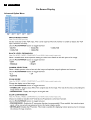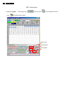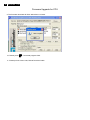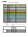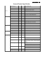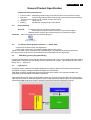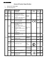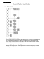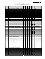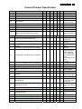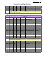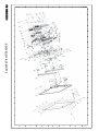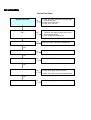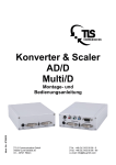
1
42 inch FHD LCD PUBLIC DISPLAY BDL4230E/00 Horizontal frequencies 31 - 8 3 kHz TABLE OF CONTENTS Description Page Description Page Important Safety Notice--------------------------------------2 Technical Data--------------------------------------------------3 Installation----------------------------------------------------4~6 Failure Mode Of Panel - ------------------------------------47 Wiring Diagram----------------------------------------------48 Block Diagram-------------------------------------------49~50 Troubleshooting------------------------------------------------7 On Screen Display----------------------------------------8~19 Scaler Diagram & C.B.A. -----------------------------51~55 Power Diagram & C.B.A. ----------------------------56~58 Control Diagram & C.B.A. ----------------------------59~60 Philips Pixel Defect Policy ---------------------------------20 Mechanical Instructions ------------------------------21~26 Color adjustment ---------------------------------------27~28 Electrical instruction -----------------------------------29~31 Service Tool-----------------------------------------------32~33 DDC Instructions & Serial Number -----------------34~41 DDC DATA ----------------------------------------------------42 Firmware Upgrade for CPU-- -------------------------43~46 SAFETY General product specification---------------------61~110 Exploded V iew ---------------------------------------------111 Spare/ Recommended P arts List-----------------------112 PCBA photos-------------------------------------------------113 Repair tips---------------------------------------------114~115 Repair Flow chart------------------------------------116~121 Safety Test Requirments---------------------------------122 NOTICE ANY PERSON ATTEMPTING TO SERVICE THIS CHASSIS MUST FAMILIARIZE HIMSELF WITH THE CHASSIS AND BE AWARE OF THE NECESSARY SAFETY PRECAUTIONS TO BE USED WHEN SERVICING ELECTRONIC EQUIPMENT CONTAINING HIGH VOL TAGES. CAUTION: USE A SEPARATE ISOLATION TRANSFORMER FOR THIS UNIT WHEN SERVICING. REFER TO BACK COVER FOR IMPORTANT SAFETY GUIDELINES Published by Philips Consumer Lifestyle Copyright reserved Subject to modification Aug 21 2009 GB 2 BDL4230E LCD Important Safety Notice Proper s ervic e and repair is important to the safe, reliable operation of all Philips Consumer Electronics Company equipment. The service procedures recommended by Philips and FOR PRODUCTS CONTAINING LASER : DANGER - described in this service manual a re eff ective methods of performing service operations . Some of these service AVOID DIRECT EXPOSURE TO BEAM. CAUTION - operations require the us e of tools speciall y desi gned for the Use of controls or adjustments or performance of procedures other than purpose. The special tools should be used when and as those specified herein may result in recomm ended. hazardous radiation exposure. It is im portant to note that this m anual c ontains various CAUTI ONS and NOTICES which should becarefully read in Invisible laser radiation when open. CAUTION - The use of optical instruments with this product will increase eye hazard. order to m inimize the risk of personal injury to service personnel . The possibility exists that improper service methods may damage the equipment. It is also important to underst and that these CAUTIONS and NOTICES ARE NOT EXHAU STIVE. Philips could not possibly know, evaluate and advise the servic etrade of all conceivable ways i n which TO ENSURE THE CONTINUED RELIABILITY OF THIS service might be done or of the possible hazardous PRODUCT , USE ONLY ORIGINAL MANUFACTURER'S consequences of each way. Consequently, Philips has not REPLACEMENT PAR TS, WHICH ARE LISTED WITH THEIR PART undertaken any such broad evaluation. Accordingly, NUMBERS IN THE PARTS LIST SECTION OF THIS who uses a servi ce procedure or tool which is not SERVICE MANUAL. recommended by Philips must first satisfy himself thoroughly that neither his safety nor the safe operation of the equipment will be jeopardized by the service method selected. * * Hereafter throughout this manual, Philips Consumer Electronics Company will be referred to as Philips . * * Take care during handling the LCD module with backlight unit - Must mount the module using mounting holes arranged in four WARNING corners. - Do not press on the panel, edge of the frame strongly or electric Critical components having special safety characteristics are identified with a by the Ref. No. in the parts list and enclosed within a broken line shock as this will result in damage to the screen. - Do not scratch or press on the panel with any sharp objects, such as pencil or pen as this may result in damage to the panel. (where several critical components are grouped in one area) along with the safety symbol on the schematics or exploded views. - Protect the module from the ESD as it may damage the electronic circuit (C -MOS). Use of substitute replacement parts which do not have the - Make certain that treatment body are grounded through same speci fied safety characteristic s may create shock, fire, wrist band. or other hazards . - Do not leave the module in high temperature and in areas of high Under no circumstances should the original design be humidity for a long time. modified or altered without written permission from Philips. Philips assumes no liability, express or implied, arising out of - Avoid contact with water as it may as hort circuit within the module. - If the surface of panel become dirty, please wipe it off with a soft any unauthorized modification of design. Servicer assumes all liability. material. (Cleaning with a dirty or rough cloth may damage the panel.) BDL4230E LCD Technical Data LGD panel Interface Requirement LCD Panel LCD size Display Resolution Pixel Pitch LC420WUN-SBA1 42.02” inch 1920(H) x 1080(V) 0.4845 mm Viewing Angle R/L 178 degree (min)/ UD178 degree (min) Display Response Time (Tr+Tf) Display Color Contrast Ratio Luminance Surface 3H, Lamp Life Time 5 ms (G-to-G) 1.06B (10bits) 1400:1(Typ) 500 cd/m2 (Typ.) Haze10% 50,000hrs (Min.) External Connector 1 1920 x 1080 @ 60 Hz 8-bit 162 MHz ADC Picture in Picture(PIP) Yes Yes 3D comb-filter, 3D De-interlace Yes Fully Programmable White Balance functions Enhanced H & V Sharpness PC Auto Phase adjustment and Auto Mode Detect Advanced video enhance. noise reduction RS232 control in and out Screen saver with image sticking protection 0 1 1 1 0 0 1 1 0 1 1 2 2 VGA (D-sub) DVI Audio (PC) HDMI Yes Yes Component (YPbPr) Yes Yes VGA input and output Yes Display wall support up to 5x5 Yes Remote control lock in OSD Front panel keypad lock Yes Yes Scheduling Y HDMI Overscan Auto Adjustment es Yes Yes Audio (RCA/YPbPr) Built-in AC power board 1 1 1 1 1 1 0 RS232 AV (VIDEO) BNC/CBVS Power Requirement Power Supply 1 Power hard switch Yes Yes Configuration Output 1 Power (AC) Features Max & Native Panel Resolution Input S-Video By pass AC plug-in for external BOX PC Power Cable Detachable AC power cord Power Supply AC power adaptor: 90~264V AC 50/60Hz Voltage Power Consumption Environment Requirement Operating Condition Power ON mode: < TBD W Operating Temperature Standby mode: < 1 W Humidity Off mode < 1 W Altitude DPMS Support Power Saving Mode <1 W Power Control On/off control via IR/RS232/Push button Temperature 0 to 40 degrees к Relative Humidity: 85%@50к (non-condensing) 0 meter to +3000 meters above sea level Storage Condition Temperature Temperature-20 to 60 degree к Humidity Relative Humidity: 10~85%@50к (non-condensing) Altitude 0 meter to 12,000 meters above sea level 3 4 BDL4230E LCD Installation Front View Product Description Input/ Output Terminals Rear View Remote Control BDL4230E LCD Using s-video input Using video input Package Contents Using HDMI input Connecting external equipment (DVD/ VCR/VCD) Using component video input Connecting a PC Using VGA input 5 6 BDL4230E LCD Using DVI input Using DVI input External audio connection Connecting external speakers Connecting external audio device Connecting another BDL4230E monitor BDL4230E LCD 7 Troubleshootingʳ Symptom Possible Cause Remedy 1. The power cord is disconnected. No picture is displayed 2. The main power switch on the back of the 1. Plug in the power cord. monitor is not switched on. 2. Make sure the power switch is switched on. 3. 3. The selected input has no connection. Connect a signal connection to the monitor. 4. The monitor is in standby mode in VGA mode. Interference displayed on the Caused by surrounding electrical appliances, monitor or audible noise is heard cars/motorcycles or fluorescent lights. Color is abnormal The signal cable is not connected properly Move the monitor to another location to see is the interference is reduced. Make sure that the signal cable is attached firmly to the back of the monitor. 1. Make sure that the signal cable is attached firmly. Picture is distorted with abnormal patterns 1. The signal cable is not connected properly. 2. Check the video signal source to see if it is 2. The input signal is beyond the capabilities of beyond the range of the monitor. Please verify its the monitor. specifications with this monitor’s specification section. Display image doesn’t fill up the full size of the screen Can hear sound, but no picture Use the ZOOM MODE or CUSTOM ZOOM function The zoom mode is not correctly set. in the SCREEN menu to fine tune display geometry and time frequency parameter. Improperly connected source signal cable. Make sure that both video inputs and sound inputs are correctly connected. 1. Make sure that both video inputs and sound 1. Improperly connected source signal cable. Can see picture but no sound is 2. Volume is turned all the way down. heard inputs are correctly connected. 2. Use VOL UP/VOL DOWN button to hear sound. 3. MUTE is turned on. 3. Switch MUTE off by using the MUTE button. 4. No external speaker connected 4. Connect external speakers and adjust the volume to a suitable level. This monitor is manufactured using an extremely Some picture elements do not light up Some pixels of the display may not turn on. high level of precision technology: however, sometimes some pixels of the monitor may not display. This is not a malfunction. After-Images can still be seen on the monitor after the monitor is powered off. (Examples of still pictures include logos, video games, computer images, and images displayed in 4:3 normal mode) A still picture is displayed for an over extended period of time Do not allow a still image to be displayed for an extended period of time as this can cause a permanent after-image to remain on the monitor. 8 BDL4230E LCD On-Screen Display Description of the On Screen Displayʳ What is the On-Screen Display?ʳ On-Screen Display (OSD) is a feature in all Philips LCD monitors. It allows an end user to adjust screen performance or select functions of the monitors directly through an on-screen instruction window. A user friendly on screen display interface is shown as below:ʳ Picture Menu ʳ ʳ ʳ ʳ ʳ ʳ ʳ ʳ ʳ ʳ BDL4230E LCD 9 On-Screen Display ʳ ʳ ʳ ʳ 10 BDL4230E LCD On-Screen Display Screen Menu ʳ ʳ ʳ ʳ BDL4230E LCD 11 On-Screen Display ʳ ʳ ʳ ʳ ʳ ʳ ʳ ʳ ʳ ʳ ʳ ʳ ʳ ʳ ʳ ʳ ʳ ʳ ʳ 12 BDL4230E LCD On-Screen Display Audio Menu ʳ BDL4230E LCD On-Screen Display PIP Menu 13 14 BDL4230E LCD On-Screen Display Configuration 1 Menu BDL4230E LCD On-Screen Display Configuration 2 Menu 15 16 BDL4230E LCD On-Screen Display Advanced Option Menu BDL4230E LCD On-Screen Display 17 18 BDL4230E LCD On-Screen Display BDL4230E LCD On-Screen Display 19 20 BDL4230E LCD Philips Pixel Defect Policyʳ Philips' Flat Panel Displays Pixel Defect Policyʳ Philips strives to deliver the highest quality products. We use some of the industry's most advanced manufacturing processes and practice stringent quality control. However, pixel or sub-pixel defects on the PDP / TFT panels used in Plasma- & LCD- displays are sometimes unavoidable. No manufacturer can guarantee that all panels will be free from pixel defects, but Philips guarantees that any Plasma- & LCD- displays with an unacceptable number of defects will be repaired during the warranty period in line with your local guarantee conditions. This notice explains the different types of pixel defects and defines the acceptable defect level for the BDL4230E LCD screen. In order to qualify for repair under warranty, the number of pixel defects must exceed a certain level which is given in the reference table. If the LCD screen is within specification a warranty exchange / claim back will be refused. Additionally, because some types or combinations of pixel defects are more noticeable than others, Philips sets even higher quality standards for those. Pixels and Sub pixels A pixel, or picture element, is composed of three sub-pixels in the primary colors of red, green and blue. Many pixels together form an image. When all sub-pixels of a pixel are lit, the three colored sub-pixels together appear as a single white pixel. When all are dark, the three colored sub-pixels together appear as a single black pixel. Other combinations of lit and dark sub-pixels appear as single pixels of other colors. Proximity of Pixel Defects ʳ Because pixel and sub-pixels defects of the same type that are nearby one another may be more noticeable, Philips also specifies tolerances for the proximity of pixel defects. In the table below you can find specifications about: • Allowed amount of adjacent dark dots = (adjacent dark dots =1 pair of dark dots) • Minimum distance between dark dots • Total no. of all defective dots Pixel Defect Tolerances In order to qualify for repair due to pixel defects during the warranty period, a PDP / TFT panel in a Philips Plasma / LCD- display must have pixel or sub-pixel defects exceeding the tolerances listed in the following table. BRIGHT DOT DEFECTSʳ ACCEPTABLE LEVEL BDL4230Eʳ MODELʳ 1 lit sub pixelʳ 3ʳ 2 adjacent lit sub pixelsʳ 1ʳ 3 adjacent lit sub pixels (one white pixel) 0 50% ~ Less Dot (Weak Dot) 7 Distance between two bright dot defects* 5mm Total bright dot defects of all types BLACK DOT DEFECTSʳ 7 ACCEPTABLE LEVEL BDL4230Eʳ MODELʳ Types of Pixel Defects + Dot Definition Pixel and sub-pixel defects appear on the screen in different ways. There are three categories of pixel defects and several types of sub-pixel defects within each category. Dot definition = What is a defective "Dot"? : One or more defective, adjacent sub-pixel are defined as one "dot". The no. of defective sub-pixels are not relevant to define a defective dot. This means that a defective dot can consist of one, two or three defective sub-pixels which can be dark or lit. 1 dark sub pixelʳ 9ʳ 2 adjacent dark sub pixelsʳ 3ʳ 3 adjacent dark sub pixelsʳ 1ʳ Distance between two black dot defects*ʳ NAʳ Total black dot defects of all typesʳ TOTAL DOT DEFECTSʳ 9ʳ ACCEPTABLE LEVEL MODELʳ Bright Dot Defects Bright dot defects appear as pixels or sub-pixels that are always lit or "on". These are the examples of bright dot defects: TOTAL DOT DEFECTS OF ALL TYPESʳ Note: * 1 or 2 adjacent sub pixel defects = 1 dot defect One lit red, green or blue sub-pixel Two adjacent lit sub-pixels: - Red + Blue = Purple - Red + Green = Yellow Green + Blue = Cyan (Light Blue) Three adjacent lit sub-pixels (one white dot) Dark Dot Defects Black dot defects appear as pixels or sub-pixels that are always dark or "off". These are the examples of black dot defects One dark dot l Two adjacent dark dots = 1 pair of dark dots Green = Yellow Green + Blue = Cyan (Light Blue) Two dark dots, specifications defines the minimum distance between dark dots BDL4230Eʳ 10ʳ BDL4230E LCD 21 Mechanical Instruction Preparation before disassemble 1.Clean the room for disassemble 2.Identify the area for monitor 3.Check the position that the monitors be placed and the quantity of the monitor ;prepare the area for material flow; according to the actual condition plan the disassemble layout 4.Prepare the implement, equipments, materials as bellow: 1) Press-fixture 2) working table 3) Screw-driver 4) knife*1 5) glove 6) cleaning cloth 7) ESD protection item picture Operation Tool Disassemble the VESA 1 Screw-driver bktÆ 12 screws, After take off speakers of connector 2 disassembly the bezel from the monitor take off 17 pcs screw, ! Screw-driver Notes 22 BDL4230E LCD Mechanical Instruction 3 disassembly the transfer Screw-driver board from the case rear take off 2 pcs screw, After take off 2wires from transfer board 4 Disassembled the keypad from the case rear take off wire ˦˶̅˸̊ʳ˅̃˶̆ ! Screw-driver BDL4230E LCD Mechanical Instruction 5 Take off 2 pcs screw Screw-driver 6 Take off 3 pcs screw Screw-driver 7 Take off 3 pcs tape 8 Disassembled the speakers form vesa bkt take off 4 screws ! Screw-driver 23 24 BDL4230E LCD Mechanical Instruction 9 Take off 2 tapes from bzl ,After disassemble IR lens 10 Take off 17 screws Screw-driver 11 Disassemble the I/O bkt Screw-driver and top bkt Æ take off 6 screws ! BDL4230E LCD Mechanical Instruction 12 Disassemble the wires Æ1 screw ! Screw-driver 25 26 BDL4230E LCD Mechanical Instruction 13 Disassemble power bd , Screw-driver audio bd, main bd,Æ15 screws 14 Take off 17 screws from Screw-driver 4side of case rear 15 Disassemble the handles Screw-driver Æ4 screws 16 Tear out the acetic tape 7pcs 17 Disassemble the R,L bkt Æ 12 Screws 18 Tear out the acetic tape 12 pcs and disassemble wires ! Screw-driver BDL4230E LCD 27 Color Adjustment Color adjustment (1). Input source set the YPbPr (VGA / DVI / HDMI) input (2). After ADC Calibration (3). Set the picture mode to standard mode at user OSD (4). Set input timing to SDTV480P with“80% white” pattern (5). Enter factory OSD, select Color Temp Turning. (6). Use CA210 read the color coordinate. (7). Adjust the Red, Green, Blue driver to let the color coordinate to meet the table1 spec. (8). Go to step (6) until the 80% white pattern meet the table 1 spec. (9). Add the following “offset” values to drive/offset values of 10000°KColor Temperature to get9300°K Color Temperature. (10). Add the following “offset” values to drive/offset values of 6500°KColor Temperature to get 5800°K Color Temperature. (3). (4). (5). (6). YPbPr (VGA / DVI / HDMI) Color Temp 9300° K (1). (2). R drive G drive B drive R offset G offset B offset 10000° K R -2 10000° K G +0 10000° KB +5 10000° K R +0 10000° KG +0 10000° KB +0 Timing SDTV480P @ 60Hz , YPbPr source DEFAULT the unit and select the ANSI BRIGHTNESS GRID pattern. Change the unit to MAX/MAX for Contrast/Brightness , Color temperature default setting 9300°K. Surface luminance is luminance value at point 1 across the LCD surface 50cm from the surface with all pixels displaying white. From more information see Fig. When VDDB =24V,IDDB = 12.5 A. LWH=Lon1, Where Lon1 is the luminance with all pixels displaying white at center 1 location. just for reference , no spec. Position the CA-210 at the locations indicated on the grid , there are 9 points see Fig .1. Measure and Record the values when the GRID is OFF. Panel spec brightness minimum 400 nits , typical 500 nits , Luminance Variation 1.3(Max). The variation in surface luminance, WHITE is defined under 100% brightness as: ǻwhite(9P)=Maximum(Lon1, Lon2,…,Lon9)/Minimum(Lon1, Lon2,…Lon9) Spec and Table list Color Temp 5800°K R drive G drive B drive 6500°K R +8 6500°K G +0 6500°K B -15 R offset 6500°K R +0 G offset 6500°K G +0 B offset 6500°K B +0 (1). Reference: The variance of color coordinate via Red, Green, Blue : X Y Red drive p xp Green drive p Yp Blue drive p xn Yn Red offset n xn Green offset n Yn Blue offset n xp Yp (2). Table 1-1,1-2,1-3 : Color temperature spec User OSD (AV Signal Black Level =40Δcontrast =72) (YPbPr Signal Black Level=49, contrast =55) (VGA Signal Black Level =48, contrast = 50) Video Color adjustment (1). (2). (3). (4). (5). (6). Input source set the CVBS1 (CVBS2 / S-Video) input. Set the picture mode to standard mode at user OSD. Setup input timing to NTSC with“80% white” pattern Enter factory OSD, select Color Temp Turning Use CA210 read the color coordinate. Adjust the Red, Green, Blue driver to let the color coordinate to meet the table1 spec. (7). Go to step (5) until the 80% white pattern meet the table 1 spec. (8). Add the following “offset” values to drive/offset values of 10000°K Color Temperature to get 9300°K Color Temperature. (9). Add the following “offset” values to drive/offset values of 6500°K Color Temperature to get 5800°K Color Temperature. CVBS1 (CVBS2 / S-VIDEO) Color Temp 9300° K Color Temp 5800°K R drive G drive B drive R offset 10000° KR +0 10000° KG +0 10000° K B -8 10000° KR +0 R drive G drive B drive 6500°K R +8 6500°K G +0 6500°K B -14 R offset 6500°K R +0 G offset 10000° KG +0 10000° KB +0 G offset 6500°K G +0 B offset 6500°K B +0 Table 1-1 Color temp item @factory OSD Color temperature x y CVBS1 / CVBS2 / S-VIDEO / VGA / YPbPr / DVI / HDMI 10000qK 0.278r0.01 0.291r0.01 B offset Table 1-2 Color temp item @factory OSD Color temperature x y CVBS1 / CVBS2 / S-VIDEO / VGA / YPbPr / DVI / HDMI 9300qK 0.283r0.01 0.298r0.01 Table 1-3 Screen Uniformity Color temp item @factory OSD CVBS1 / CVBS2 / S-VIDEO / VGA / YPbPr / DVI / HDMI Color temperature x y 6500qK 0.312r0.01 0.329r0.01 Table 1-4 Fig.1 Optical measurement point Color temp item @factory OSD Color temperature x y CVBS1 / CVBS2 / S-VIDEO / VGA / YPbPr / DVI / HDMI 5800qK 0.326r0.01 0.342r0.01 28 BDL4230E LCD Color Adjustment Table 2 : default value of internal gain RGB drive & offset: Color temp item CVBS1 / CVBS2 / VGA / YPbPr / DVI @factory OSD S-VIDEO / HDMI Color temperature 10000qK 10000qK Red drive 127 127 Green drive 127 127 Blue drive 135 136 Red offset 127 130 Green offset 127 127 Blue offset 127 120 Color temp item @factory OSD Color temperature Red drive Green drive Blue drive Red offset Green offset Blue offset CVBS1 / CVBS2 / S-VIDEO 9300qK 127 127 127 127 127 127 Color temp item @factory OSD Color temperature Red drive Green drive Blue drive Red offset Green offset Blue offset CVBS1 / CVBS2 / S-VIDEO 6500qK 127 127 127 127 127 127 Color temp item @factory OSD Color temperature Red drive Green drive Blue drive Red offset Green offset Blue offset CVBS1 / CVBS2 / S-VIDEO 5800qK 135 127 113 127 127 127 Table 3 : limit value of RGB drive & offset: Color temp item CVBS1 / CVBS2 / @factory OSD S-VIDEO Color temperature 10000qK Red drive 100~140 Green drive Blue drive Red offset 110~140 Green offset Blue offset Color temp item @factory OSD Color temperature Red drive Green drive Blue drive Red offset Green offset Blue offset VGA / YPbPr / DVI / HDMI 9300qK 127 127 127 137 127 127 VGA / YPbPr / DVI / HDMI 6500qK 127 127 127 127 127 127 VGA / YPbPr / DVI / HDMI 5800qK 135 127 112 127 127 127 VGA / YPbPr / DVI / HDM 10000qK 100~140 110~140 CVBS1 / CVBS2 / VGA / YPbPr / S-VIDEO DVI / HDMI 9300qK 9300qK 110~130 110~130 110~140 110~140 Color temp item @factory OSD Color temperature Red drive Green drive Blue drive Red offset Green offset Blue offset CVBS1 / CVBS2 / VGA / YPbPr / S-VIDEO DVI / HDMI 6500qK 6500qK Color temp item @factory OSD Color temperature Red drive Green drive Blue drive Red offset Green offset Blue offset CVBS1 / CVBS2 / VGA / YPbPr / S-VIDEO DVI / HDMI 5800qK 5800qK 110~130 110~130 110~140 110~140 100~140 100~140 110~140 110~140 PC Auto Timing Check (1) Timing list: Resolution 800×600 Horizontal Frequency (KHz) 37.879 Vertical Dot Clock Frequency Frequency (Hz) (MHz) 60.317 40.0 Remark VESA (2) Setup input timing VESA-800x600 (37.9K, 60Hz) “16-Grays pattern” pattern. (3) Select timing from above timing list. (4) If position is wrong, press “Auto Adjust” function at user OSD to check this function PC (RGB) ADC Calibration (1) Setup input timing VESA-800x600 (37.9K, 60Hz) & 16-Grays pattern to DSUB connector. (2) Setup “source” to “VGA”. (3) Select 16:9 format (4) Enter factory OSD (5) Enter the “ADC CAL….” page and run “Calibration…” function (6) Execute “Input 16 grays scale pattern for PC” to start calibration. 4. YPbPr ADC Calibration: (1) Setup input timing SDTV480P & “SMPTE Color Bar (0 IRE, 75% Color)” pattern to component connectors. (2) Setup “source” to “YpbPr”. (3) Select 16:9 format. (4) Enter factory OSD. (5) Enter the “ADC CAL….” page and run “Calibration” function. (6) Execute “Input SMPTE 75 color bar for 480P” to start calibration BDL4230E LCD 29 (OHFWULFDO,QVWUXFWLRQV Electrical characteristics ¾ 1. PC input signal requirements display engine is 720 physical lines in wide aspect z Pixel rate capability -86 MHz. z VGA sync input - TTL level, separate H/V sync only, “+” or “-” polarity, terminated with t 2.2k: impedance. The minimum native resolution of the display or ratio. z Video Interfaces: ¾ The display device accepts HD input via: z HDMI input Analog YPbPr. “HD ready” displays support analog YPbPr as a HD input format TMDS channel: ¾ Carries video data. to allow full compatibility with today's HD ¾ Signaling method: According to DVI 1.0 video sources in the market. Support of the specification. Single-link (Type A HDMI). YPbPr signal should be through common ¾ Video pixel rate: 25 MHz to 165 MHz (Type A) industry standard connectors directly on the HD ready display or through an adaptor DDC channel: ¾ Allows source to interrogate capabilities of sink. ¾ I²C signaling with 100 kHz clock. ¾ E-EDID data structure according to EIA/CEA-861B and VESA Enhanced EDID. z VGA analog RGB level - 0 ~ 700mV linear, positive polarity, terminated with 75: impedance. z I²C DDC signal - DDC2B required, DDC serial Data & Clock, DDC components are connected to both display Vcc and DDC +5V (from PC via video cable), that the easily accessible to the consumer; and ¾ HDMI HD capable inputs accept the following HD video formats: 1280x720 @ 50 and 60Hz progressive scan (“720p”) 1920x1080 @ 50 and 60Hz interlaced (“1080i”) ¾ The HDMI input supports copy protection (HDCP). PC can read the DDC data also when the display is z FHD-FHD ready logo not required, but powered off. To prevent current feedback into PC, requirements to be fulfilled as:1080p/23.98, 1080p/24, blocking diodes are required at display side. 1080p/25, 1080p/29.97, 1080p/50, and 1080p/60. z Audio input -Sensitivity 500mVrms, the amplifier outputs full power when the input level reaches 500mVrms, terminated with impedance >10k:. z Lineout output - Stereo, 2Vrms output. z HDMI Input -Compliance with HDMI Specification 1.3 or later, 480i/p, 576i/p, 720p, 1080i/p signal handling capability. z Speaker output - 2 x 10 Wrms back firing speakers, with T.H.D. < 10%. 2. AV input signal requirements z CVBS input -1000mVpp (including 300 mV sync level), terminated with input impedance of 75:. z S-Video input - Y: 1000mVpp, C: 300mVpp, terminated with input impedance of 75:. z Component video input -Y: 1000mVpp, PbPr: ±350mVpp, terminated with input impedance of 75:. 480i/p, 576i/p, 720p, 1080i signal handling capability. z HD ready -HD ready logo not required, but requirements to be fulfilled as-Display, display engine: TMDS channel: ¾ Carries audio, video and auxiliary data. ¾ Signaling method: According to HDMI Ver. 1.3b specification. (Type A HDMI). ¾ Video pixel rate: 25 MHz to 165 MHz (Type A) ¾ Pixel encodings: RGB 4:4:4, YCbCr 4:2:2, YCbCr 4:4:4. ¾ Audio sample rates: 32 kHz, 44.1 kHz, 48 kHz, 88.2 kHz, 96kHz, 176.4 kHz, 192 kHz. ¾ Audio channels: up to 8. 30 BDL4230E LCD Electrical Instructions DDC channel: z ¾ Allows source to interrogate capabilities of sink. Audio input -Sensitivity 500mVrms, the amplifier ¾ I²C signaling with 100 kHz clock. outputs full power when the input level reaches ¾ E-EDID data structure according to EIA/CEA-861B 500mVrms, terminated with input impedance of >10k:. z and VESA Enhanced EDID. Speaker output -Back firing speakers 2 x 10 Wrms, with T.H.D. < 10%. Content protection: ¾ According to High-Definition Content Protection z No signal input - While no signal at external inputs, screen goes blue before entering standby mode. (HDCP) Specification 1.10. 3. Timing requirement MODE STANDARD x x RESOLUTION ASPECT RATIO HANDLING ʳ FS*Full-Screen AR Aspect Ratio Composite S-Video YPBPR RGB HDMI DVI VESA 640x480 @ 60Hz 1920x 1080 16:09 NA NA NA Y Y Y VESA 640x480 @ 72Hz 1920x 1080 16:09 NA NA NA Y Y Y VESA 640x480 @ 75Hz 1920x 1080 16:09 NA NA NA Y Y Y ʳ 720x400 @ 70Hz 1920x 1080 16:09 NA NA NA Y Y Y VESA 800x600 @ 60Hz 1920x 1080 16:09 NA NA NA Y Y Y VESA 800x600 @ 75Hz 1920x 1080 16:09 NA NA NA Y Y Y VESA 1024x768 @ 60Hz 1920x 1080 16:09 NA NA NA Y Y Y ʳ 1024x768 @ 75Hz 1920x 1080 16:09 NA NA NA Y Y Y VESA 1280 x 768 @ 60Hz 1920x 1080 16:09 NA NA NA Y Y Y VESA 1280 x 800 @ 60Hz 1920x 1080 16:09 NA NA NA Y Y Y VESA 1280x960 @ 60Hz 1920x 1080 16:09 NA NA NA Y Y Y VESA 1280x1024 @ 60Hz 1920x 1080 16:09 NA NA NA Y Y Y VESA 1360 x 768 @ 60Hz 1920x 1080 16:09 NA NA NA Y Y Y VESA 1366 x 768 @ 60Hz 1920x 1080 16:09 NA NA NA Y Y Y VESA 1600x1200 @ 60Hz 1920x 1080 16:09 NA NA NA Y Y Y VESA 1920x1080 @ 60Hz 1920x 1080 16:09 NA NA NA Y Y Y VESA 1920x1200 @ 60Hz 1920x 1080 16:09 NA NA NA Y Y Y PAL 576i(50Hz) 1920x 1080 16:09 Y Y Y NA Y NA NTSC 480i(60Hz) 1920x 1080 16:09 Y Y Y NA Y NA DVD 480p(60Hz) 1920x 1080 16:09 NA NA Y NA Y NA ʳ 576p(50Hz) 1920x 1080 16:09 NA NA Y NA Y NA ʳ 720p(50Hz) 1920x 1080 16:09 NA NA Y NA Y NA ʳ 720p(60Hz) 1920x 1080 16:09 NA NA Y NA Y NA ʳ 1080i (50Hz) 1920x 1080 16:09 NA NA Y NA Y NA ʳ 1080i (60Hz) 1920x 1080 16:09 NA NA Y NA Y NA ʳ 1080p(50Hz) 1920x 1080 16:09 NA NA Y NA Y NA ʳ 1080p(60Hz) 1920x 1080 16:09 NA NA Y NA Y NA * = Default Setting, ** = these modes also works on every source input. Aspect Ratio control is saved to memory, tied to input. BDL4230E LCD 31 (OHFWULFDO,QVWUXFWLRQV White color adjustment The picture color temperature shall be able to be chosen out of 5 modes 10000K,9300K, 6500K, 5800K, and USER. 10000K, 9300K, 6500K, 5800K are factory setting (fixed color) and “USER” is adjustable mode. (The default color of “USER” mode is the same color as 6500K mode.) A/D converter calibration of the scalar shall be performed with 0V/0.730Vp-p black/white level signal to obtain adequate dynamic range for video signal output level deviation. White balance adjustment and inspection shall be carried out using 0.700Vp-p level signal. Measurement condition – Measurement point : Center of screen Measurement distances Measurement Angle Measurement equipment – Color Analyzer Signal Generator Video Signal : 50cm : 90° : CA210 or Equivalent : VG828 or Equivalent : White pattern Color Temperature Table: Mode x y Specification 10000K 0.278 0.291 ±0.03 9300K 0.283 0.298 ±0.03 6500K 0.313 0.329 ±0.03 5800K 0.326 0.342 ±0.03 32 BDL4230E LCD Service tool-Hardware F/W Writing Tool: RS232 Cable: P/N Description 5K.0R505.501 CABLE D-SUB 9/9P UL20276 11M EDID Writing Tool: USB Cable and Jig BD P/N Description 5K.L1E03.501 Service Tool-Cable-VOARD (CABLE USB 2.0A/B B-PVC 1.8M) 5E.0RC38.001 Service Tool-Board-VOARD (PCBA JIG BD MI WP42SF0) BDL4230E LCD Service tool-Software FW writing tool: Pixelworks ImageProcessor SDK FlashUpgrader EDID writing tool: RTD_CustomerTool_V1.2 33 34 BDL4230E LCD DDC Instructions DDC Data Re-programming In case the DDC data memory IC or main EEPROM which storage all factory settings were replaced due to a defect, the serial numbers have to be re-programmed "Analog DDC IC, Digital DDC IC & EEPROM". It is advised to re-soldered DDC IC and main EEPROM from the old board onto the new board if circuit board have been replaced, in this case the DDC data does not need to be re-programmed. Additional information Additional information about DDC (Display Data Channel) may be obtained from Video Electronics Standards Association (VESA). Extended Display Identification Data(EDID) information may be also obtained from VESA. Configuration and procedure 1.Install ϘCustomerTool_V1.2ϙ in PC or NB 2. Press ϘYϙ to install DriverLINX Port I/O Driver BDL4230E LCD DDC Instructions 3. Follow the installed steps and press ϙNEXTϙ to Install Driver 4. When setup has finished, restart computer 35 36 BDL4230E LCD DDC Instructions 5. Prepare the download equipment. - Use USB cable connect to PC and Tool Board - Use VGA cable connect to Tool Board and Display PC or NB VGA cable for EDID writing need to be removed pin5 to disable EDID write protect Display 6. Plug power cord into Display and run ϘDebugTool_V6.2ϙ file OK Fail BDL4230E LCD DDC Instructions 7. Update EDID – select “EDID Update” Communication – select “USB”, ISP Type – select “Serial Flash” For EDID Updated 37 38 BDL4230E LCD DDC Instructions 8. EDID upload(VGA) Ω EDID length select press and then press to select EDID file and then to write EDID into display 128B for VGA Open EDID file To write EDID BDL4230E LCD DDC Instructions (Power off status and LED: Red) 9. EDID upload(DVI)-EDID length select and then press to select EDID file and then press to write EDID into display 128B for DVI Open EDID file To write EDID 39 40 BDL4230E LCD DDC Instructions (Power off status and LED: Red) 10. EDID upload(HDMI) Ω EDID length select press and then press to select EDID file and then to write EDID into display 256B for VGA Open EDID file To write EDID 11. EDID upload finished and successful as below BDL4230E LCD DDC Instructions Serial Number Definition 41 42 BDL4230E LCD DDC DATA Analog DDC 00 FF FF FF FF FF FF 00 41 0C 05 D2 00 00 00 00 01 14 01 03 08 5D 34 78 EA 6F C3 A3 55 49 9A 24 10 47 4A AD 4A 00 81 80 81 40 A9 40 81 00 01 01 01 01 01 01 01 01 02 3A 80 18 71 38 2D 40 58 2C 45 00 A2 0B 32 00 00 1E 00 00 00 FF 00 52 41 4B 30 39 30 31 30 30 30 30 31 0A 00 00 00 FD 00 32 4 C 1 F 4 B 11 0 0 0 A 2 0 2 0 20 20 20 20 00 00 00 FC 00 50 48 4C 20 42 44 4C 34 32 33 30 45 0A 00 D5 Decoded EDID data DVI DDC 00 41 01 EA 10 81 01 80 45 00 30 31 4C 20 00 34 FF 0C 14 6F 47 40 01 18 00 00 39 0A 1F 20 50 32 FF FF FF FF FF 00 05 D2 00 00 00 00 01 03 80 5D 34 78 C3 A3 55 49 9A 24 4A AD 4A 00 81 80 A9 40 81 00 01 01 01 01 01 01 02 3A 71 38 2D 40 58 2C A2 0B 32 00 00 1E 00 FF 00 52 41 4B 30 31 30 30 30 30 00 00 00 FD 00 32 4 B 11 0 0 0 A 2 0 2 0 20 20 00 00 00 FC 48 4C 20 42 44 4C 33 30 45 0A 00 5D HDMI DDC 00 41 01 EA 10 81 01 80 45 00 30 31 4C 20 00 34 02 14 06 83 10 2D 32 71 A2 56 33 66 40 00 00 00 FF 0C 14 60 47 40 01 18 00 00 39 0A 1F 20 50 32 03 04 07 01 00 40 00 1C 0B AA 00 21 70 1E 00 00 FF 05 01 D7 4A A9 01 71 A2 00 30 00 4B 20 48 33 22 13 15 00 02 58 00 16 32 51 A2 50 36 00 00 00 FF FF FF FF 00 D2 00 00 00 00 03 80 5D 34 78 A3 55 4A 9B 24 AD 4A 00 81 80 40 81 00 01 01 01 01 01 02 3A 38 2D 40 58 2C 0B 32 00 00 1E FF 00 52 41 4B 31 30 30 30 30 00 00 FD 00 32 11 0 0 0 A 2 0 2 0 20 00 00 00 FC 4C 20 42 44 4C 30 45 0A 01 55 F1 4F 90 1F 05 11 1 2 0 1 0 2 0 3 15 23 09 7F 07 00 65 03 0C 00 3A 80 18 71 38 2C 45 00 A2 0B 1E 01 1D 80 18 20 58 2C 25 00 00 00 9E 66 21 00 1E 30 46 8F 0B 32 00 00 1E B0 51 00 1B 30 00 A2 0B 32 00 00 00 00 00 00 00 00 00 00 00 00 00 00 00 20 BDL4230E LCD Firmware Upgrade for CPU 1. Preparation: 1.1 Tool: f Download cable( RS232 cable connect between PC/Notebook with tool board ) f #RS232 is RXD and TXD interlaced line f Personal computer or Notebook f Download tool program “Pixelworks ImageProcessor SDK FlashUpgrader”. 1.2 Firmware files 2. Procedure: 1. Open firmware program files 2. Choose FlashUpgrar.exe files. 43 44 BDL4230E LCD Firmware Upgrade for CPU 3. Show the Pixelworks ImageProcess K FlashUpgrader picture. #The Connection, COM Port in accordance with user by oneself PC/NB choose. #The Notify On Completion in accordance with user by oneself PC/NB choose. 4. The RS232 Download cable insert RS232 INPUT pin. 5. Press Flash key of Pixelworks ImageProcess or SDK FlashUpgrader BDL4230E LCD Firmware Upgrade for CPU 6. The key change to cancel after Press Flash key, 7. The Power code cable insert. 8. The pixelworks ImageProcess or SDK FlashUpgrader program download start. 45 46 BDL4230E LCD Firmware Upgrade for CPU 9. The firmware download will finish after about 5 minutes. 10. Please press “確定”. Download program finish. 11. Please pull out Power code, RS232 Download cable. BDL4230E LCD 47 Failure Mode Of Panel Quick reference for failure mode of LCD panel this page presents problems that could be made by LCD panel. It is not necessary to repair circuit board. Simply follow the mechanical instruction on this manual to eliminate failure by replace LCD panel. Failure description Vertical block defect Polarizer has bubbles Phenomenon Polarizer has bubbles Vertical dim lines Foreign material inside polarizer . It shows liner or dot shape. Vertical lines defect (Always bright or dark) Concentric circle formed Horizontal block defect Bottom back light of LCD is brighter than normal Horizontal dim lines Back light un-uniformity Horizontal lines defect (Always bright or dark) Has bright or dark pixel Backlight has foreign material. Black or white color, liner or circular type Power BD Audio BD 48 BDL4230E LCD J2 IR BD J1 Transfer BD J1 J2 B4 01 B4 02 B4 03 Wiring Diagram J11 J24 J1 J20 Keypad Main BD J21 Panel J25 Block Diagram BDL4230E LCD 49 50 BDL4230E LCD Block Diagram A B C D 5 0.1U K C71 0.1U K 0.1U K C94 C93 0.1U K C91 0.1U K 0.1U K C90 C92 0.1U K C89 A1V8 0.1U K C86 0.1U K C84 0.1U K 0.1U K C83 C85 10UF K C82 Z120 AVCC33 R365 4.7K 3 2HDMI_CKN 3 2HDMI_CKP 10 HDMI_INT 3 H2_HPD AVCC18 HPD1 2HDMI_CKN 2HDMI_CKP I2C_SEL DVCC18 DSDA0 DSCL0 RP WR0 1HDMI_D2N 1HDMI_D2P 1HDMI_D1N 1HDMI_D1P 1HDMI_D0N 1HDMI_D0P HDMI1 INPUT R471 3.3K LSCL LSDA C393 10UF K 3 H1DDC_SDA 3 H1DDC_SCL 3 H1_RPWR5V 3 1HDMI_D2N 3 1HDMI_D2P 3 1HDMI_D1N 3 1HDMI_D1P 3 1HDMI_D0N 3 1HDMI_D0P AVCC33 AVCC33 L8 A3V3 11 11 21 22 23 24 25 26 27 28 29 30 31 32 33 34 35 36 37 38 39 40 4 R415 22 J R416 22 J R0X0R0X0+ AVC33 R0X1R0X1+ AGND R0X2R0X2+ AVCC18 DSDA0 DSCL0 RPWR0 DVCC18 DGND I2CSEL/INT# HPD1 AVCC18 R1CR1C+ AGND U24 SII9185ACTU 2HDMI_D2N 2HDMI_D2P D3V3 AVCC18 I2C Pull high TP221 TP222 HDMI2 INPUT D1V8 HDMI OUTPUTPUT R472 750 3 Scalar Diagram & C.B .A DSDA1 DSCL1 RP WR1 3.3K TP220 HDMI_RST add R 500 ohm 3 3 RESET 1HDMI_CKP 1HDMI_CKN 1HDMI_CKP 1HDMI_CKN AVCC18 2HDMI_D0N 2HDMI_D0P HPD2 R470 H1_HPD 2HDMI_D0N 2HDMI_D0P AVCC33 2HDMI_D1N 2HDMI_D1P 2HDMI_D1N 2HDMI_D1P AGND I2CADDR/TPWR TSCL TSDA HPDIN RSVDL DGND DVCC18 RPWR2 DSCL2 DSDA2 AVCC18 R2X2+ R2X2AGND R2X1+ R2X1AVCC33 R2X0+ R2X0- AVCC18 4 TXCTXC+ TXCTXC+ 7,11 TX1- 3 TX0TX0+ TX0TX0+ AVCC18 TX1TX1+ 2HDMI_D2N 2HDMI_D2P3 3 H2DDC_SDA H2DDC_SCL 3 H2_RPWR5V3 D VII_CKN DVI_CKP 3 3 DVI_HPDET 3 DVI_CKN 3 DVI_CKP 3 5 TX1+ 7 7 TX2TX2+ 7 7 TX2TX2+ 20 19 18 17 16 15 14 13 12 11 10 9 8 7 6 5 4 3 2 1 AGND R0C+ R0CAVCC18 HPD0 LSCL/EPSEL1 LSDA/EPSEL0 RESET# EXT_SWING TXCTXC+ AGND TX0TX0+ AVCC18 TX1TX1+ AGND TX2TX2+ R1X0R1X0+ AVCC33 R1X1R1X1+ AGND R1X2R1X2+ AVCC18 DSDA1 DSCL1 RPWR1 CEC_D CEC_A AVCC33 HPD2 AVCC18 R2CR2C+ AGND 41 42 43 44 45 46 47 48 49 50 51 52 53 54 55 56 57 58 59 60 AVCC33 3 80 79 78 77 76 75 74 73 72 71 70 69 68 67 66 65 64 63 62 61 7 7 4 DVI_D1P DVI_D1N AVCC33 DVI_D0P DVI_D0N RP WR2 DSCL2 DSDA2 AVCC18 DVI_D2P DVI_D2N DVCC18 4 4 DVI_D0P DVI_D0N DVI INPUT 4 4 4 4 DVI_D1P DVI_D1N DVI_D2P DVI_D2N DVI_RPWR5V 4 DVIDC_SCL 4 DVIDC_SDA 4 TPWR TPWR 7 TSCL HDDC_SCL 7 TSDA HDDC_SDA 7 HP DIN HDMI_HPDET 10 R167 4.7K 7 7 4 4 D1V8 C88 C87 2 0.1U K 0.1U K C383 10UF K 2 TSCL TSDA R396 4.7K R395 4.7K D3V3 1 1 A B C D BDL4230E LCD 51 A B C D 4.7K R178 6 6 6 6 6 6 6 6 I2S_WS I2S_CLK I2S_DA_IN0 RCLK48B R177 * 4.7K /NC D3V3 0x62/0x6A TP63 WS SCK C133 R188 1M 28.322MHZ Y1 RXO C134 R184 390 change to 5 PF 33 R179 DAC_MUTE TPWR XI Audio_CLK R181 RWS R183 RSCK TP60 R0PWR5V XO TP62 33 33 TP58 TP57 TP56 69 70 TP54 TP55 6 35 30 95 94 89 81 82 83 84 85 86 78 75 105 65 66 TP51 TP53 51 52 HDMI_D2N HDMI_D2P 61 62 47 48 HDMI_D1N HDMI_D1P 57 58 43 44 HDMI_D0N HDMI_D0P TP48 TP49 39 40 TP46 TP47 TX2TX2+ TX1TX1+ TX0TX0+ TXCTXC+ SD0 Address 0x60/0x68 (Default) HDMI_CKN HDMI_CKP HDMI_SCDT R419 100 HDMI_RST HDMI2_DSDA HDMI2_DSCL HDMI1_DSDA HDMI1_DSCL R0PWR5V R1PWR5V XTALIN XTALOUT MCLK SD0 SD1 SD2 SD3 WS SCK SPDIF MUTEOUT CI2CA R1X2R1X2+ R1X1R1X1+ R1X0R1X0+ R1XCR1XC+ R0X2R0X2+ R0X1R0X1+ R0X0R0X0+ R0XCR0XC+ U25A INT Remove 1 2 TP279 * 20P J /NC C137 4.7K R170 4 R197 Y2 Vcont 4 3 4 * 0 J/NC Vdd Output * 18.432MHZ/NC GND Option SiI9125 34 33 DSCL0 DSDA0 TP225 29 28 DSCL1 DSDA1 TP42 TP43 LAYOUT: Place xtal circuit as compact and close to chip as possible Default High State Low 1 101 100 RESET# RX Config. I2C Addr. Select 2 102 INT SCDT VREF 0.01U K C95 22 19 20 21 5 RSVDNC RSVDNC RSVDNC RSVDNC RSVDL CSDA CSCL Q32 Q33 Q34 Q35 Q28 Q29 Q30 Q31 Q24 Q25 Q26 Q27 Q20 Q21 Q22 Q23 Q16 Q17 Q18 Q19 Q12 Q13 Q14 Q15 Q8 Q9 Q10 Q11 Q4 Q5 Q6 Q7 Q0 Q1 Q2 Q3 D3V3 4 3 2 1 4 3 2 1 4 3 2 1 RN3 5 6 7 8 RN4 5 6 7 8 R180 R182 RN5 5 6 7 8 RN6 5 6 7 8 33 J 33 J TP50 TP52 HDMI_G/Y0 HDMI_G/Y1 HDMI_G/Y2 HDMI_G/Y3 HDMI_G/Y4 HDMI_G/Y5 HDMI_G/Y6 HDMI_G/Y7 HDMI_G/Y8 HDMI_G/Y9 TP59 TP61 HDMI_R/Cr0 HDMI_R/Cr1 HDMI_R/Cr2 HDMI_R/Cr3 HDMI_R/Cr4 HDMI_R/Cr5 HDMI_R/Cr6 HDMI_R/Cr7 HDMI_R/Cr8 HDMI_R/Cr9 CSDA R185 CSCL R186 141 140 139 138 135 134 133 132 129 128 127 126 123 122 121 120 117 116 115 114 111 110 109 108 26 27 R0PWR5V 4.7K 4 3 2 1 R175 R176 HDMI_B/Cb6 HDMI_B/Cb7 HDMI_B/Cb8 HDMI_B/Cb9 3 2 1 144 R187 4 3 2 1 RN2 5 6 7 8 10 9 8 7 55 76 77 98 99 4 3 2 1 RN1 5 6 7 8 HDMI_B/Cb2 HDMI_B/Cb3 HDMI_B/Cb4 HDMI_B/Cb5 AGND C135 0.1U K Z120 L12 IN0G[0..9] IN0B[0..9] 3 Audio_CLK I2S_CLK I2S_DA_IN0 I2S_WS 22K R597 12 13 15 14 1 2 3 16 TEST DEMP FMT MUTE BCK DATA LRCK SCK U26 IN0R[0..9] 10UF K C136 10 10 TP505 R195 22 J R196 22 J R193 22 J R194 22 J CDCLK : 2.3 MHz SLRCLK : 48 KHz AGND SCLK : 18.432 MHz DAC_MUTE L26 Z30 3 +5V_Module CSDA_HDMI 11 CSCL_HDMI 11 IN0R6 IN0R7 IN0R8 IN0R9 IN0R2 IN0R3 IN0R4 IN0R5 IN0R0 IN0R1 IN0G6 IN0G7 IN0G8 IN0G9 IN0G2 IN0G3 IN0G4 IN0G5 IN0G0 IN0G1 IN0B6 IN0B7 IN0B8 IN0B9 IN0B2 IN0B3 IN0B4 IN0B5 IN0B0 IN0B1 BOM Remove 33 33 33 J 33 J 33 33 33 J 33 J 33 33 R173 R174 33 J 33 J C96 * 0.1U K/NC IN0_TMD_DE 10 IN0_TMD_HS 10 IN0_TMD_VS 10 IN0_TMD_CLK 10 TP44 TP45 HDMI_B/Cb0 HDMI_B/Cb1 33 J 33 J 33 J 33 16 15 14 13 RDE R168 RHSY NC R169 R VSYNC R171 RODCK R172 PORT2_CLK Resister must close with AD_CLK Resister and close to T2 SIL9125CTU EVNODD DE HSYNC VSYNC ODCK 6 HDDC_SDA 6 HDDC_SCL 3 AGND NC ZEROA VCOM VOUTR VOUTL 10 5 11 10 8 7 10UF K10UF K 10UF K C138 1U K C432 1U K C394 Z120 L11 C124 0.1U K C119 0.1U K C117 0.1U K C116 0.1U K C114 0.1U K C112 0.1U K C110 0.1U K C108 0.1U K C106 0.1U K C104 0.1U K C102 0.1U K C129 C130 Z120 L10 VCOM_F D3V3 D1V8 D1V8 10UF K C100 0.1U K C98 2 L9 8 2 HDMI_AOR 8 HDMI_AOL 0.1U K C131 10 HDMI_SCDT 6,11 HDMI_RST 4 0.1U K C132 11 9125_INT G1 97 96 92 93 37 54 72 38 42 46 50 56 60 64 68 36 41 45 49 53 59 63 67 71 D3V3 *NC_1U K C395 11 Buzzer_PWM EPAD REGVCC XTALVCC DVCC18 DGND2 AVCC18 AVCC18 AVCC18 AVCC33 AVCC33 AVCC33 AVCC33 AVCC33 AVCC33 AVCC33 AVCC33 AGND AGND AGND AGND AGND AGND AGND AGND AGND U25B Z120 AGND 1U K +12V SiI9125 C400 1 10UF K C397 4.7K R468 C396 10P J AGND 9.1K R467 N.C 4 3 2 1 V+ B_IN+ B_IN- B_OUT 12 24 25 80 91 107 119 131 143 11 23 79 90 106 118 130 142 6 18 32 74 88 104 113 125 137 4 17 31 73 87 103 112 124 136 5 6 7 8 D1V8 D3V3 1 *NC_NJM3414AV-TE1 V- A_IN+ A_IN- A_OUT U17 SIL9125CTU CVCC18 CVCC18 CVCC18 CVCC18 CVCC18 CVCC18 CVCC18 CVCC18 CVCC18 CGND CGND CGND CGND CGND CGND CGND CGND IOVCC33 IOVCC33 IOVCC33 IOVCC33 IOVCC33 IOVCC33 IOVCC33 IOVCC33 IOVCC33 IOGND IOGND IOGND IOGND IOGND IOGND IOGND IOGND IOGND LAYOUT: Place capacitors as close as possible to chip R465 5 0.1U K C99 AGND + +12V C128 0.1U K C127 0.1U K C126 0.1U K C125 0.1U K C123 0.1U K C122 0.1U K C121 0.1U K C120 0.1U K C118 0.1U K C115 0.1U K C113 0.1U K C111 0.1U K C109 0.1U K C107 0.1U K C105 0.1U K C103 0.1U K C101 0.1U K 10UF K C97 1 Scalar Diagram & C.B .A 6 VCC PCM1754DBQR DGND C133 27P J AGND 10K J 4 C134 33P J 10P J 10K J R191 C398 R192 9 * 22K F/NC R466 10K J 22K F R190 2 52 BDL4230E LCD CLK_OUT B A C399 *NC_47U 25V <Spec> R469 3.3 C D A B C SV_Y1 1,10 0.1U K 0.1U K 0.1U K 0.1U K 0.1U K 0.1U K 0.1U K 0.1U K 0.1U K 0.1U K 0.1U K C333 C334 C335 C336 C337 C339 C340 C341 C342 C343 C344 5 C366 0.1U K C365 0.1U K VDD1V8 4.7K 0.1U K C367 0.1U K C368 11 VDC_RSTn 2 POWER_STB VDD3V3 VDD3V3 R357 R355 22 J R356 22 J 0.1U K C332 8,11 CPN_SCL 8,11 CPN_SDA 10 VDC_IRQ VDD3V3 SV_C1 10 CVBS_IN2 1,10 1,10 CVBS_IN1 TP200 1 2 3 4 5 6 7 8 9 10 11 12 13 14 15 16 17 18 19 20 21 22 23 24 25 26 27 28 29 30 31 32 0.1U K C369 VDC_PWDN VDC_A3V3 VDC_A1V8 *NC_14.318MHZ 0.1U K C370 R359 A33GND A33VDD VI_1 VI_2 VI_3 NC VI_4 VI_5 VI_6 NC A18VDD A18GND A18VDD A18GND A18GND A18VDD VI_7 VI_8 VI_9 NC VI_10 VI_11 VI_12 NC A33VDD A33GND A33GND A33GND DGND SCL SDA INTREQ U41 C330 27P J C331 22P J R349 VDD1V8 VDD3V3 PORT2_VS TP196 PORT2_HS TP197 TP198 PORT2_FIELD TP199PORT2_SOG/DEN R348 10K Address : 0xB8 *TVP5160PNP /NC 0.1U K C371 0 0.1U K C372 4 R360 10K P3V3 Z120 L51 C356 0.1U K 0.1U K C357 VDD3V3 VDC_DQ8 VDC_DQ9 VDC_DQ10 VDC_DQ11 VDC_DQ12 VDC_DQ13 VDC_DQ14 VDC_DQ15 VDC_DQ7 VDC_DQ6 VDC_DQ5 VDC_DQ4 VDC_DQ3 VDC_DQ2 VDC_DQ1 VDC_DQ0 R358 3 C358 0.1U K C359 3 0.1U K C360 0.1U K VDC_BA0 VDC_RAS VDC_CAS VDC_WE P3V3 C349 * 10P/NC 22uF C362 X5R ==> 10uF x7R 0.1U K VDC_BA0 VDC_BA1 0.1U K C363 R354 10K VDC_A3V3 10UF K C373 R353 10K 2 VDC_DQ7 VDC_DQ5 VDC_DQ6 VDC_DQ3 VDC_DQ4 VDC_DQ1 VDC_DQ2 VDC_DQ0 C364 0.1U K Z120 Z120 L50 U42 VSS DQ15 VSSQ DQ14 DQ13 VDDQ DQ12 DQ11 VSSQ DQ10 DQ9 VDDQ DQ8 VSS N.C/RFU UDQM CLK CKE N.C A11 A9 A8 A7 A6 A5 A4 VSS C346 C352 0.1U K C347 0.1U K C353 0.1U K 0.1U K C354 0.1U K C348 54 53 52 51 50 49 48 47 46 45 44 43 42 41 40 39 38 37 36 35 34 33 32 31 30 29 28 1 0.1U K 0.1U K C355 C350 VDC_A11 VDC_A9 VDC_A8 VDC_A7 VDC_A6 VDC_A5 VDC_A4 0.1U K C351 VDC_SDRAM_CLK VDC_SDRAM_CLK VDC_DQ8 VDC_DQ10 VDC_DQ9 VDC_DQ12 VDC_DQ11 VDC_DQ14 VDC_DQ13 VDC_DQ15 A B C D BDL4230E LCD 53 * M12L64164A-7TG/NC VDD DQ0 VDDQ DQ1 DQ2 VSSQ DQ3 DQ4 VDDQ DQ5 DQ6 VSSQ DQ7 VDD LDQM WE CAS RAS CS BA0 BA1 A10/AP A0 A1 A2 A3 VDD 0.1U K VDD1V8 0.1U K C345 L49 1 2 3 4 5 6 7 8 9 10 11 12 13 14 15 16 17 18 19 20 21 22 23 24 25 26 27 VDC_A1V8 VDD3V3 PORT2_VIDEO[9..0] 10 VDC_SDRAM_DQM VDC_WE VDC_CAS VDC_RAS VDC_SDRAM_CS VDC_BA0 VDC_BA1 VDC_A10 VDC_A0 VDC_A1 VDC_A2 VDC_A3 10 P1V8 VDC_CLK PORT2_VIDEO[9..0] VDC_SDRAM_DQM VDC_WE VDC_CAS R352 VDC_RAS *10M/NC VDD3V3 R351 *10M/ NC VDD3V3 C338* 10P/NC PORT2_VIDEO6 PORT2_VIDEO7 PORT2_VIDEO8 PORT2_VIDEO9 PORT2_VIDEO2 PORT2_VIDEO3 PORT2_VIDEO4 PORT2_VIDEO5 2 measure VDC_A3V3 ripple value modify C373 value 0.1U K C361 Z120 L52 VDC_SDRAM_CLK VDC_SDRAM_DQM VDC_BA0 VDC_RAS VDC_CAS VDC_WE VDC_A4 VDC_A5 VDC_A6 8 7 6 5 8 7 6 5 RN24 R350 33 VDC_BA1 1 2 3 4 22RN23 1 2 3 4 22 VDD1V8 PORT2_VIDEO0 R477 22 J PORT2_VIDEO1 VDC_SDRAM_CS VDC_A3 VDC_A2 VDC_A1 VDC_A0 VDC_A10 VDC_BA1 VDD3V3 R476 22 J VDC_A7 VDC_A8 VDC_A9 VDC_A11 33VDC_SDRAM_CLK VDC_SDRAM_DQM Y_2 Y_3 Y_4 IOGND IOVDD Y_5 Y_6 Y_7 Y_8 Y_9 DGND DVDD DATACLK GLCO/GPIO/I2CA0 GPIO/I2CA1 A3 A2 A1 A0 A10 BA1 IOGND IOVDD BA0 RAS# CAS# WE# A4 A5 A6 DGND DVDD 96 95 94 93 92 91 90 89 88 87 86 85 84 83 82 81 80 79 78 77 76 75 74 73 72 71 70 69 68 67 66 65 PORT2_VS 10 PORT2_HS 10 PORT2_FIELD 10 PORT2_SOG/DEN 10 10K Thermal_Pad D Y5 TP249 R347 100K TP250 4 TP251 G1 5 XTAL2 XTAL1 Scalar Diagram & C.B .A TP252 TP253 TP254 128 127 126 125 124 123 122 121 120 119 118 117 116 115 114 113 112 111 110 109 108 107 106 105 104 103 102 101 100 99 98 97 A33GND Analog_out A33GND A33VDD PLL18GND PLL18VDD XTAL2 XTAL1 DGND FSS VS/VBLK/GPIO HS/CS/GPIO FID/GPIO AVID/GPIO C_0/GPIO C_1/GPIO DGND DVDD C_2/GPIO C_3/GPIO C_4/GPIO C_5/GPIO IOGND IOVDD C_6/GPIO/DR C_7/GPIO/DG C_8/GPIO/DB C_9/GPIO/FSO DGND DVDD Y_0 Y_1 DVDD DGND PWDN RESETB IOVDD IOGND D0 D1 D2 D3 D4 D5 D6 D7 DVDD DGND D15 D14 D13 D12 D11 D10 D9 D8 IOVDD IOGND DQM CLK A11 A9 A8 A7 33 34 35 36 37 38 39 40 41 42 43 44 45 46 47 48 49 50 51 52 53 54 55 56 57 58 59 60 61 62 63 64 54 BDL4230E LCD Scalar Diagram & C.B .A Scalar Diagram & C.B .A BDL4230E LCD 55 56 BDL4230E LCD Power Diagram & C.B.A BDL4230E LCD Power Diagram & C.B.A 57 58 BDL4230E LCD Power Diagram & C.B.A A B C D 2K D 1005112 J1 G2 12 11 10 9 8 7 6 5 4 3 2 1 G1 5 5 H1 S cr e w Hole s TP4 TP6 H2 T P 10 TP9 TP7 TP8 TP5 TP3 TP2 TP1 H3 2 C1 0 .1U K H4 4 4 H5 68 F R2 1_R 3_G R E D /G R N 3 OP 2 OP O ptical P oints OP 1 OP 2 OP 3 OP OP 4 OP OP 5 OP OP 6 OP V9 1 5 V 150P F C9 0 .1U K V8 1 5 V 150P F C8 0 .1U K V7 1 5 V 1 50P F C7 0 .1U K V6 1 5 V 150P F C6 0 .1U K V5 1 5 V 150P F C5 0 .1U K V4 1 5 V 150P F 68 F R1 LE D1 3 Control Diagram & C.B .A. C4 0 .1U K V3 1 5 V 150P F C3 0 .1U K V2 1 5 V 1 50P F C2 0 .1U K V1 1 5 V 150P F . . 1 2 . . 1 2 . . 1 2 . . 1 2 . . 1 2 . . 1 2 . . 1 2 . . 1 2 . . 1 3 1 2 S K R P AB E 010 SW7 1 4 2 3 S K R P A B E 010 3 1 4 3 4 2 S K R P AB E 010 SW4 2 S K R P AB E 010 SW1 1 SW6 4 3 S K R P A B E 010 2 1 SW5 4 3 S K R P AB E 010 2 1 SW2 2 4 2 3 1 1 S K R P A B E 010 SW3 1 4 2 BDL4230E LCD 59 vC o d A B C D 60 BDL4230E LCD Control Diagram & C.B .A. BDL4230E LCD General Product Specification Product Identification 42” BDL LCD DISPLAY BDL4230E/00 Issued by: Technical Marketing Manager Larry Yang 61 62 BDL4230E LCD General Product Specification Table of Contents 1. SCOPE ......................................................................................................................... 5 1.1 GENERAL PRODUCT FEATURES.................................................................................................................. 5 1.2 PRODUCT RANGE ....................................................................................................................................... 5 2. ELECTRICAL REQUIREMENTS ......................................................................................... 5 2.1 STANDARD TESTING CONDITIONS ................................................................................................................ 5 2.2 VIDEO / AUDIO INPUT SIGNALS .................................................................................................................... 6 2.2.1 PC input signal requirements ....................................................................................................... 6 2.2.2 AV input signal requirements ....................................................................................................... 8 2.3 DDC CHANNEL ........................................................................................................................................... 9 2.4 SERVICE MODE ......................................................................................................................................... 10 2.5 POWER SUPPLY ......................................................................................................................................... 10 2.5.1 Power supply features....................................................................................................... 10 2.5.2 Power consumption .......................................................................................................... 10 2.5.3 Display DPM standby (D-sub & HDMI input) ....................................................................... 10 2.6 USER CONTROL INTERFACE........................................................................................................................ 10 2.6.1 Hidden controls ................................................................................................................ 10 2.6.2 Front controls ................................................................................................................... 11 2.7 I /O CONNECTORS ..................................................................................................................................... 27 3. VISUAL PERFORMANCE................................................................................................ 28 3.1 LCD MODULE CHARACTERISTICS .............................................................................................................. 28 3.2 FRONT OF SCREEN PERFORMANCE ............................................................................................................. 28 4. FUNCTIONAL REQUIREMENTS ....................................................................................... 29 4.1 POWER ................................................................................................................................................... 29 4.2 PICTURE .................................................................................................................................................... 29 4.2.1 Wide Screen Signalling Bit (WSSB) picture size ................................................................. 29 4.2.2 Picture format ................................................................................................................... 30 4.2.3 Picture in Graphics ........................................................................................................... 30 4.3 AUDIO ...................................................................................................................................................... 30 4.3.1 Sound mode..................................................................................................................... 30 4.3.2 Sound related requirements .............................................................................................. 31 4.4 PICTURE SHIFTING .................................................................................................................................... 31 4.5 PC PICTURE AUTO ADJUSTMENT FUNCTION ----- D-SUB INPUT ................................................................... 31 4.6 ESP (ENERGY SAVING PROGRAMMABILITY) .............................................................................................. 31 4.7 LIGHT SENSOR ......................................................................................................................................... 31 4.8 HEAT MONITORING AND DEFINITION........................................................................................................... 32 4.9 SMART POWER ......................................................................................................................................... 32 5. NON FUNCTIONAL REQUIREMENTS................................................................................ 32 5.1 START UP BEHAVIOR ................................................................................................................................. 32 5.2 DEFAULT/RESET CONTROL VALUES ........................................................................................................... 32 5.3 TIME-OUT ................................................................................................................................................. 33 5.4.1 Audio last status ............................................................................................................... 33 5.4.2 Video last status ............................................................................................................... 33 5.4.3 Function last status ........................................................................................................... 33 5.5 CHANNEL TABLES ..................................................................................................................................... 33 5.6 LIFE TIME INDICATION (SHOW ON OSD MENU TO BE DEFINED) .................................................................... 33 5.7 EXTERNAL COMMUNICATION..................................................................................................................... 33 6. ACCESSORIES ............................................................................................................ 34 6.1 CABLES ..................................................................................................................................................... 34 6.2 REMOTE CONTROL ................................................................................................................................... 34 6.3 DFU....................................................................................................................................................... 34 6.4 QUICK USER GUIDE ................................................................................................................................. 34 6.5 WARRANTY CARD .................................................................................................................................... 34 6.6 OTHERS ................................................................................................................................................... 34 7. MECHANICAL .............................................................................................................. 34 7.1 COSMETIC ................................................................................................................................................ 34 7.2 MECHANICAL DATA FILES .......................................................................................................................... 34 BDL4230E LCD 63 General Product Specification 7.3 LOCATION OF PHILIPS LOGO..................................................................................................................................35 7.4 LOCATION OF ICONS.................................................................................................................................. 35 7.5 COLOR FOR RESIN / PAINT ......................................................................................................................... 35 7.6 RESINS ..................................................................................................................................................... 35 7.7 PAINT USED ............................................................................................................................................... 35 7.8 PLASTIC MOLD TOOLING ............................................................................................................................ 35 7.9 PLASTICS FLAMMABILITY ............................................................................................................................ 35 7.10 TEXTURE/GLOSSING OF HOUSING ............................................................................................................. 35 7.11 BASE TILT / SWIVEL RANGE ...................................................................................................................... 35 7.12 MOVEMENT OF UNIT WITH BASE................................................................................................................ 35 7.13 WALL MOUNT METHOD ............................................................................................................................ 36 7.14 LABEL...................................................................................................................................................... 36 7.15 PRODUCT DIMENSION / WEIGHT................................................................................................................ 36 7.16 TRANSPORTATION .................................................................................................................................... 36 7.16.1 Transportation packages............................................................................................................. 36 7.16.2 Transportation test procedures ................................................................................................... 36 7.17 PALLET / CONTAINER LOADING ................................................................................................................. 36 8. RELIABILITY / ENVIRONMENT .......................................................................................... 37 8.1 MTBF PREDICTION..................................................................................................................................... 37 8.2 DEMONSTRATION MTBF ............................................................................................................................ 37 8.3 TEMPERATURE ........................................................................................................................................... 37 8.4 HUMIDITY................................................................................................................................................... 37 8.5 ALTITUDE................................................................................................................................................... 37 8.6 AIR PRESSURE ........................................................................................................................................... 37 8.7 ENVIRONMENTAL TEST .............................................................................................................................. 37 9. REGULATORY COMPLIANCE ......................................................................................... 38 9.1 WORLDWIDE REGULATORY ....................................................................................................................... 38 9.2 EMC REQUIREMENTS ............................................................................................................................... 39 9.4 ROHS...................................................................................................................................................... 39 9.5 WEEE ..................................................................................................................................................... 39 9.6 ONGOING REGULATORY ............................................................................................................................ 39 10. DQE Test Items Template ............................................................................................... 39 10.1SYSTEM FLOW CHART ............................................................................................................................... 40 10.2SPECIFICATION INPUT AND UPDATE ............................................................................................................ 40 10.3DESIGN QUALITY EVALUATION CAPABILITY QUALIFICATION ........................................................................... 40 10.4QUALITY AND RELIABILITY DELIVERABLES LIST ............................................................................................ 41 10.5 DESIGN QUALITY AND RELIABILITY REVIEW AND VALIDATION PROCEDURE ..................................................... 49 10.6 DESIGN QUALITY REVIEW AND VALIDATION EVALUATION PROCESS ............................................................... 49 10.7 DESIGN CHANGE REVIEW AND CONFIRMATION ............................................................................................ 49 10.8 DESIGN QUALITY IMPROVEMENT ................................................................................................................ 50 10.8.1 Customer complaints................................................................................................................... 50 10.8.2 Field Call Rate ............................................................................................................................. 50 10.8.3 Analyze root cause & Work out solution ..................................................................................... 50 10.8.4 Verify solution effectiveness........................................................................................................ 50 10.8.5 Review issue technical report...................................................................................................... 50 10.8.6 Verification of ECN ...................................................................................................................... 50 10.8.7 Update the deliverables list ......................................................................................................... 50 64 BDL4230E LCD General Product Specification DOCUMENT REVISION HISTORY Revision no. V0.9 Date 2009/09/25 2009/10/27 Description Draft for discussion Revise for final spec. BDL4230E LCD 65 General Product Specification 1. SCOPE This specification describes the feature and performance of the LCD public/business display, which includes PC video connector for Display application and AV connectors for multiple video format inputs. x Product Name - x Manufacturer ID - PHL (in EDID) x Product ID - D205 (in EDID) x Serial no. - xxxx (in EDID & NVM) 1.1 x x x x x x x x x x x x x x x x x x x x x PHL BDL4230E (in EDID) General Product Features Screen of 16:9 aspect ratio, 42” Full HD LCD color display Universal power supply PC analog 15pin D-sub input/output Supports PC mode via D-sub, DVI and HDMI connector Multi-system PAL, SECAM, NTSC playback Support components video, S-Video, composite video input and audio input. Support HDMI Ver.1.3b. with HDCP, audio included (meet EIA-861B standard) User-friendly and family look OSD menu User-friendly and professional look remote controller DPM power management for PC mode VESA standard wall mount Portrait mounting (extra ventilation slots have to be considered) Tiled matrix up to 5x5 Software upgrade should be done easily Network controllability through RS-232 Smart Power Fault diagnostics Advanced anti image sticking Automatic Long Cable Compensation PIP/POP/PBP support Scheduling 1.2 Product Range Display Destination Mains Cord BDL4230E/00 EU, NA, China EU, UK, NA, CN 2. Cabinet Color ELECTRICAL REQUIREMENTS All performance specifications are defined under “STANDARD TESTING CONDITIONS”, unless otherwise specified. 2.1 x x x x x x Standard Testing Conditions Warm up time - t 30 min. Ambient temperature - 15qC ~35 qC. Ambient light 400-600 lux Relative humidity 25% ~ 75%. Barometric pressure - 860 mbar ~ 1013 mbar. Dark room conditions - < 1 lux for optical measurements 66 BDL4230E LCD General Product Specification 2.2 Video / Audio Input Signals 2.2.1 PC input signal requirements z z z Pixel rate capability 86 MHz. VGA sync input TTL level, separate H/V sync only, “+” or “-” polarity, terminated with t 2.2k: impedance. HDMI input TMDS channel: ¾ Carries video data. ¾ Signaling method: According to DVI 1.0 specification. Single-link (Type A HDMI). ¾ Video pixel rate: 25 MHz to 165 MHz (Type A) DDC channel: ¾ Allows source to interrogate capabilities of sink. ¾ I²C signaling with 100 kHz clock. ¾ E-EDID data structure according to EIA/CEA-861B and VESA Enhanced EDID. z z VGA analog RGB level -0 ~ 700mV linear, positive polarity, terminated with 75: impedance. z I²C DDC signal DDC2B required, DDC serial Data & Clock, DDC components are connected to both display Vcc and DDC +5V (from PC via video cable), that the PC can read the DDC data also when the display is powered off. To prevent current feedback into PC, blocking diodes are required at display side. Preset timings 53 preset modes sets, 15 factory preset mode sets, timing, size and centering have been pre-aligned in factory according to specifications. Preset mode definition: z Need to support those timing: BDL4230E LCD 67 General Product Specification Req. ID Resolution according to VESA DMT standard Specification ʳ Resolution Refresh Horizontal Pixel Clock Standard Type Rate Frequency PCRES4 640 x 480 60 Hz 31.5 kHz 25.175 MHz Industry Standard n/a Original Document Date n/a PCRES5 640 x 480 72 Hz 37.9 kHz 31.500 MHz VESA Standard VS901101 12/2/92 PCRES6 640 x 480 75 Hz 37.5 kHz 31.500 MHz VESA Standard VDMT75HZ 10/4/93 PCRES9 800 x 600 60 Hz 37.9 kHz 40.000 MHz VESA Guidelines VG900602 8/6/90 PCRES11 800 x 600 75 Hz 46.9 kHz 49.500 MHz VESA Standard VDMT75HZ 10/4/93 PCRES16 1024 x 768 60 Hz 48.4 kHz 65.000 MHz VESA Guidelines VG901101A 9/10/91 PCRES18 1024 x 768 75 Hz 60.0 kHz 78.750 MHz VESA Standard VDMT75HZ 10/4/93 PCRES23 1280 x 768 60 Hz 47.8 kHz 79.500 MHz CVT AddDMT 3/Apr/2003 PCRES28 1280 x 800 60 Hz 49.7 kHz 79.500 MHz CVT 1/May/2007 PCRES32 1280 x 960 60 Hz 60.0 kHz 108.000 MHz VESA Standard VDMTPROP 3/1/96 PCRES35 1280 x 1024 60 Hz 64.0 kHz 108.000 MHz VESA Standard VDMTREV 12/18/96 PCRES39 1360 x 768 60 Hz 47.7 kHz 85.500 MHz VESA Standard AddDMT 2003/4/3 PCRES41 1366 x 768 60 Hz 47.7 kHz 85.500 MHz VESA Standard AddDMT 2007/11/30 PCRES53 1600 x 1200 60 Hz 75.0 kHz 162.000 MHz VESA Standard VDMTREV 12/18/96 PCRES70 1920 x 1080 60 Hz 67.5 kHz 148.500 MHz VESA Standard VDMTREV 2007/11/30 PCRES71 1920 x 1200 60 Hz 74.0 kHz 154.000 MHz CVT Red. Blanking AddDMT 2003/4/3 PCRES89 720x400 ʳ ʳ 70 Hz DOS ʳ PCRES90 All supported resolutions will meet the timings specified separately in paragraphs in the VESA ʳ and Industry Standards and Guidelines for Computer Display Monitor Timing (DMT) Version 1.0, ʳ Revision 11, May 1 2007 or higher VIRES1 1080i@50 50Hz ʳ ʳ HD interlaced ʳ VIRES2 1080i@60 60 Hz ʳ ʳ HD interlaced ʳ VIRES3 720p@50 50Hz ʳ ʳ HD progressive ʳ VIRES4 720p@60 60 Hz ʳ ʳ HD progressive ʳ VIRES5 576i 50Hz ʳ ʳ SD PAL ʳ VIRES6 576p 50Hz ʳ ʳ ED ʳ VIRES7 480i 60Hz ʳ ʳ SD NTSC ʳ VIRES8 480p 60Hz ʳ ʳ ED ʳ VIRES9 1080p@50 50Hz ʳ ʳ Full HD ʳ VIRES10 1080p@60 60Hz ʳ ʳ Full HD ʳ Factory preset mode definition (green highlhigh light): 1. Perfect FOS while presenting those timing 2. Will specify those timing in User's Manual. z User modes - 10 user mode sets, user timings can be stored by first in first out. Auto adjustment can be used for optimal picture performance. User mode definition: 1. Can save those timing that not in Preset mode and can be showed (not over scalar or Panel spec.) 2. Usually need to reserve around 10 sets in memory User mode timing specifications: besides timings listed in VESA-timing DMT, CVT; some other special detailed timings are listed as below. 68 BDL4230E LCD General Product Specification z z z z z 85Hz timings can display, but don’t guarantee Picture. 1920X1080 should not be scaled. The position must be center. The outside area of display must be black. Audio input - Sensitivity 500mVrms, the amplifier outputs full power when the input level reaches 500mVrms, terminated with impedance >10k:. Lineout output Stereo, 2Vrms output. Speaker output 2 x 10 Wrms back firing speakers, with T.H.D. < 10%. 2.2.2 AV input signal requirements z CVBS input 1000mVpp (including 300 mV sync level), terminated with input impedance of 75:. z S-Video input - z Component video input Y: 1000mVpp, PbPr: ±350mVpp, terminated with input impedance of 75:. 480i/p, 576i/p, 720p, 1080i signal handling capability. z HD ready - z FHD z HDMI Input - Y: 1000mVpp, C: 300mVpp, terminated with input impedance of 75:. HD ready logo not required, but requirements to be fulfilled as-Display, display engine: ¾ The minimum native resolution of the display or display engine is 720 physical lines in wide aspect ratio. Video Interfaces: ¾ The display device accepts HD input via: Analog YPbPr. “HD ready” displays support analog YPbPr as a HD input format to allow full compatibility with today's HD video sources in the market. Support of the YPbPr signal should be through common industry standard connectors directly on the HD ready display or through an adaptor easily accessible to the consumer; and: ¾ HDMI HD capable inputs accept the following HD video formats: 1280x720 @ 50 and 60Hz progressive scan (“720p”) 1920x1080 @ 50 and 60Hz interlaced (“1080i”) ¾ The HDMI input supports copy protection (HDCP). FHD ready logo not required, but requirements to be fulfilled as: 1080p/23.98, 1080p/24, 1080p/25, 1080p/29.97, 1080p/50, and 1080p/60. Compliance with HDMI Specification 1.3 or later, 480i/p, 576i/p, 720p, 1080i/p signal handling capability. TMDS channel: ¾ Carries audio, video and auxiliary data. ¾ Signaling method: According to HDMI Ver. 1.3b specification. (Type A HDMI). ¾ Video pixel rate: 25 MHz to 165 MHz (Type A) ¾ Pixel encodings: RGB 4:4:4, YCbCr 4:2:2, YCbCr 4:4:4. ¾ Audio sample rates: 32 kHz, 44.1 kHz, 48 kHz, 88.2 kHz, 96kHz, 176.4 kHz, 192 kHz. ¾ Audio channels: up to 8. BDL4230E LCD 69 General Product Specification DDC channel: ¾ ¾ ¾ Allows source to interrogate capabilities of sink. I²C signaling with 100 kHz clock. E-EDID data structure according to EIA/CEA-861B and VESA Enhanced EDID. ¾ According to High-Definition Content Protection (HDCP) Specification 1.10. Content protection: z z z 2.3 x x x Audio input - Sensitivity 500mVrms, the amplifier outputs full power when the input level reaches 500mVrms, terminated with input impedance of >10k:. Speaker output Back firing speakers 2 x 10 Wrms, with T.H.D. < 10%. No signal input While no signal at external inputs, screen goes blue before entering standby mode. DDC channel E-EDID data structure according to VESA Enhanced EDID 1.3 (and EIA/CEA-861B for HDMI). Allows source to interrogate capabilities of the Display & AV inputs. Separate EDID for VGA input and HDMI input. 2.3.1 EDID content for Analog TBD 2.3.2 EDID content for Digital TBD 2.3.3 DDC/CI DDC/CI (Command Interface) specifies a means for a computer to send commands to the monitor, as well as receive sensor data from the monitor, over the bidirectional link such as DDC2Ab/Bi/B+. Specific commands to control monitors are defined in a separate Monitor Control Command Set (MCCS) standard. DDC/CI monitors are sometimes supplied with an external color sensor to allow automatic calibration of the monitor's color balance. Some tilting DDC/CI monitors support an auto pivot function, where a rotation sensor in the monitor enables the operating system to keep the display upright as the monitor is moved between its portrait and landscape positions. The following DDC/CI commands should be supported via command line: No. Commands 1 Set Brightness 2 Set Contrast 3 Set Red Gain 4 Set Green Gain 5 Set Blue Gain 6 Get Brightness 7 Get Contrast 8 Get Red Gain 9 Get Green Gain 10 Get Blue Gain 70 BDL4230E LCD General Product Specification 2.4 Service mode Detailed technical specification refers to Service delta technical specs. x Software Update: ¾ Wireless data cloning (IR transmission). ¾ Through RS-232 2.5 Power Supply 2.5.1 Power supply features x x x x x x x 2.5.2 AC line voltage range AC line frequency range DC tact switch AC mains switch Inrush current Leakage current Power factor correction - 90Vac ~ 264Vac. 50-60 Hz r 3 Hz. Minimal power consumption when switch off No power consumption when switch off. < 40A at 240Vac when cold start. < 0.5mA at 240Vac. According to EN61000-3-2 Power consumption x x x x Normal on TBD w (typical), TBD w(max.) Standby < 1w, RC standby mode Switch off (DC or TACT) - < 1w, RC in-active Switch off (AC mains) < No power consumption. 2.5.3 Display DPM standby (D-sub & HDMI input) z DPM - z Recovery from DPM - z Standby - The Display enters “AV standby mode” when it’s switched off by RC. “Standby/Power” key or SLEEP TIMER function is activated or no AV signal input for 30 minutes. z Recovery from Standby - Power & function recovers when RC “Standby” or “CH +/-” or “AV” is pressed. Hidden key control “Menu” or “CH +/-” key is toggled. The Display enters DPM off (sleep) mode when no H&V sync, one of H-sync / V-sync input or digital clock is absent. “No Video Input” message appears before entering DPM mode. A delay of 30 seconds before entering the power saving state is required to avoid misunderstanding of display resolution and timing mode changes. Power & function recover when either H & V syncs or digital clock are detected. 2.6 User Control Interface Controlled via top control keypads or remote control or RS-232. 2.6.1 Hidden controls It can’t be easily accessed in front of the set. TBC BDL4230E LCD General Product Specification To be revised according to new graphic sheet. Key PC mode AV mode DC switch power standby DC switch power standby Decrease/Volume down Decrease/Volume down Increase/Volume up Increase/Volume up Ÿ MENU Select Down Menu Select Down/Channel Down ź MENU Select Up Menu Select Up/Channel up Enter /Exit OSD menu Enter /Exit OSD menu MENU INPUT x x Power On/Off DC switch. Access main menu by pressing “MENU” key x Select function via “Ÿ / ź” keys, increase/decrease via “ x “ / / ” keys. ” are also for Volume Hot Key. 2.6.2 Front controls x LED indicator 4 States. LED Status Power Status LED behavior LED Active Normal on Blue Standby Amber RC command Blue blinking Switch off Blank LED Not-active Normal on/Standby/RC command/Switch off Blank x RC sensor – Operation Angle 0q (for H & V) 30q (for H & V) 45q (for H only) Receiver for Display control, transmitter for ITV data cloning. RC operational distance t 10m t 8m t 6m x Remote Control – Philips protocol. Philips protocol is used for remote control communication. 71 72 BDL4230E LCD General Product Specification POWER button To turn the power on/off. If LED Power Indicator on the monitor is not lightening, then the remote control will not work. SMART PICTURE button To select smart picture mode from [HIGHBRIGHT], [STANDARD], [sRGB], [CINEMA]. HIGHBRIGHT: for moving image such as Video STANDARD: for images (Factory setting) sRGB: for text based images CINEMA: for movies. PIP (Picture In Picture) button ON/OFF button: To turn PIP mode ON/OFF. INPUT button: To select the input signal for the sub-picture. CHANGE button: To exchange between the main picture and sub-picture. Note: The “PIP” and “POP” modes do not work if the screen size is “CUSTOM” or “REAL”. BDL4230E LCD General Product Specification CONTRAST button To start CONTRACT OSD selection, and then push "+" or "-" button to adjust the value. DISPLAY button To turn on/off the setting information displayed on the right-up corner of the screen. MINUS button To decrease the adjustment with OSD menu. To move the sub-picture left when in “PIP” mode. SET button To activate the setting with OSD menu. AUTO ADJUST button To execute the AUTO ADJUST function. MUTE button To turn the mute function on/off. VIDEO SOURCE button To set the video source by toggle selection from [HDMI1], [PC-A], [CVI], [VIDEO<S>] and [VIDEO]. AUDIO SOURCE button To set the audio source by toggle selection from [AUDIO1] to [AUDIO2], [AUDIO3] and [HDMI]. Note 1: You cannot select the audio source for video source is set to [VIDEO<S>] or [VIDEO]. Note 2: [HDMI] is selectable only when the video source is [HDMI 1] or [HDMI 2]. SIZE button To select the picture size from [FULL], [NORMAL], [CUSTOM] , [DYNAM IC] and [REAL]. BRIGHTNESS button To start the BRIGHTNESS OSD selection, and then push "+" or "-" button to adjust the value. UP button To move the highlight bar up to adjust the selected item when OSD menu is on. To move the sub-picture up when in “PIP” mode. MENU button To turn the OSD menu on/off. PLUS button To increase the adjustment with OSD menu. To move the sub-picture right when in “PIP” mode. EXIT button To turn to the previous OSD menu. DOWN button To move the highlight bar down to adjust the selected item when OSD menu is on. To move the sub-picture down when in “PIP” mode. VOLUME UP button To increase the audio output level. VOLUME DOWN button To decrease the audio output level. 73 74 BDL4230E LCD General Product Specification RC key definition: Remote Key Customer Code : 0x80 Data Code Function Description 0x03 Software Power ON/OFF Key Name POWER VIDEO SOURCE 0x01 Input signal select (Note1) AUDIO SOURCE 0x1E Switch Audio Input Activity 㩷 㩷 AUDIO1 -> AUDIO2 ->AUDIO3->HDMI->AUDIO1 SIZE Change the picture mode setting 0x29 Toggle the ZOOM mode PIP ON/OFF 0x24 Switch the PIP/POP and OFF PIP INPUT 0x25 Select the input source of PIP Note3 PIP CHANGE 0x26 Change the PIP/MAIN. 㩷 CONTRAST 0x27 Adjust contrast 㩷 BRIGHTNESS 0x28 Adjust Brightness 㩷 MENU 0x20 㩷 㩷 UP 0x15 㩷 㩷 DOWN 0x14 㩷 㩷 SET 0x23 㩷 㩷 PLUS 0x22 㩷 㩷 MINUS 0x21 㩷 㩷 EXIT 0x1F 㩷 DISPLAY 0x19 AUTO ADJUST 0x1C 㩷 IR control shall be set to "Normal" if the "DISPLAY" button is pushed more than 5 sec. 㩷 MUTE 0x1B Mute On/Off 㩷 VOL UP 0x17 audio volume up 㩷 VOL DOWN 0x16 audio volume down 㩷 SMART 0x1D Message display Standard -> sRGB -> Cinema -> High Bright -> Standard Note2 OFF -> PIP -> POP -> Side by Side1 -> Side by Side2 -> OFF All RC buttons generate RC commands. All those commands should be interpreted into the correct actions. 2.6.3 OSD MENU x 9 languages x OSD tree Control Picture English, French, German, Italian, Spanish, Polish, Turkish, Russian, Simple Chinese. Default Default Value Value (PC (Video Mode) Mode) Range Brightness - ʳ 0~100 Contrast ʳ ʳ 0~100 Sharpness ʳ ʳ 0~100 Black Level ʳ ʳ 0~100 BDL4230E LCD 75 General Product Specification Picture Screen ʳ PIP Configuration 1 Noise Reduction ʳ ʳ Off/Low/Middle/High Tint - ʳ 0~100 Color - ʳ 0~100 Color Temperature ʳ ʳ 5800K/6500K/9300K/10000K Color Control - ʳ R/G/B: 0~255 Light Sensor ʳ ʳ On/Off Smart Contract ʳ ʳ On/Off Video Source ʳ ʳ AV/S-Video/ VGA/DVI/HDMI/YPbPr Picture Reset ʳ ʳ No/Yes H Position ʳ ʳ 0~100 V Position ʳ ʳ 0~100 Clock - ʳ 0~100 Clock Phase - ʳ 0~100 Zoom Mode ʳ ʳ Full/Normal/Dynamic/Custom/Real Custom Zoom - ʳ ZOOM/HZOOM/VZOOM Screen Reset ʳ ʳ No/Yes Volume ʳ ʳ 0~100 Mute ʳ ʳ On/Off Audio Source ʳ ʳ Audio 1/Audio 2/Line-in/HDMI Speaker ʳ ʳ Internal/External/Line-out Audio Reset ʳ ʳ No/Yes PIP Size ʳ ʳ Small/Middel/Large PIP Audio ʳ ʳ MAIN/SUB PIP Reset ʳ ʳ No/Yes Auto Adjust - ʳ Auto/On/Off Power Save ʳ ʳ VGA: On/Off Video: On/Off Language Panel Saving English ʳ ʳ ʳ English/ German / Spanish / French / Italian / Spanish / Russian / Polish / Turkish /Simplified Chinese Cooling Fan: Auto/On/Off Brightness: Auto/Off Pixel Shift: (10~900 Seconds) Color System - ʳ Auto/NTSC/PAL/SECAM/ PAL60/4.43NTSC Configuration Reset ʳ ʳ No/Yes Factory Reset ʳ ʳ No/Yes 76 BDL4230E LCD General Product Specification Configuration 2 60 ʳ 0, 5, 10~120 Seconds OSD Mode ʳ ʳ Protrait/Landscape Information OSD ʳ ʳ Off/1~10 Seconds Sleep Timer ʳ ʳ Off/1~24 Hours OSD H Position ʳ ʳ 0~100 OSD V Position ʳ ʳ 0~100 Monitor Information ʳ ʳ Model Number OSD Turn Off Serial Number Operation Hours SW Version Advanced Option Input Resolution - ʳ Auto/1024x768/1280x768/1360x768 Black Level Expansion - ʳ Off/Low/Middle/High Gamma Selection ʳ ʳ Native/2.2/2.4 Scan Mode - ʳ Underscan/Overscan Scan Conversion - ʳ Progressive/Interlace Film Mode - ʳ Auto/Off IR Control ʳ ʳ Normal/Primary/Secondary/Lock Keyboard Control ʳ ʳ Lock/Unlock Tiling ʳ ʳ H Monitors: 1~5 V Monitors: 1~5 Position: 1~25 Frame Comp.: No/Yes Enable: No/Yes Heat Status ʳ ʳ Fan/Temperature Status Date And Time ʳ ʳ Year/Month/Day/Hour/Minute Daylight/Current Time Schedule ʳ ʳ On/Off/Input Monitor ID ʳ ʳ 1~26 DDC/CI ʳ ʳ On/Off Smart Power ʳ ʳ High/Medium/Low/Off Advanced Option Reset ʳ ʳ No/Yes BDL4230E LCD 77 General Product Specification PICTURE TBC BRIGHTNESS Adjusts the overall image and background screen brightness. Press button to increase brightness. Press button to decrease brightness. CONTRAST Adjusts the image brightness for the input signal. Press button to increase contrast. Press button to decrease contrast. SHARPNESS This function is digitally capable to keep crisp image at any timings. It is adjustable to get a distinct image or a soft one as you prefer and set independently for each picture mode. Press button to increase sharpness. Press button to decrease sharpness. BLACK LEVEL Adjusts the image brightness for the background. Press button to increase black level. Press button to decrease black level. NOTE: sRGB picture mode is standard and cannot be changed. NOISE REDUCTION * : INPUT VIDEO<S>, VIDEO only Adjusts the noise reduction level. Press button to increase reduction level. Press button to decrease reduction level. TINT * : INPUT HDMI1, 2(HDMI INPUT MODE-HD), CVI, VIDEO<S>, VIDEO only Adjusts the tint of the screen. Press button the flesh tone color becomes greenish. Press button the flesh tone color becomes purplish. 78 BDL4230E LCD General Product Specification COLOR * : INPUT HDMI1, 2(HDMI INPUT MODE-HD), CVI, VIDEO<S>, VIDEO only Adjusts the color of the screen. Press button to increase color depth. Press button to decrease color depth. COLOR TEMPERATURE Is used to adjust the color temperature. The image becomes reddish as the color temperature decreases, and becomes bluish as the color temperature increases. COLOR CONTROL The color levels of red, green, and blue are adjusted by the color bars. R: Red, G: Green, B: Blue LIGHT SENSOR It is used to turn on/off light sensor function. SMART CONTRAST It is used to turn on/off dynamic contrast ratio function. VIDEO SOURCE It is used to select video source. PICTURE RESET Selecting Picture reset allows you to reset all OSD settings about PICTURE setting. Select “Yes” and press “SET” button to restore to factory preset data. Press “EXIT” button to cancel and then return to the previous menu. SCREEN TBC H POSITION Controls Horizontal Image position within the display area of the LCD. Press button to move screen to right. Press button to move screen to left. BDL4230E LCD 79 General Product Specification V POSITION Controls Vertical Image position within the display area of the LCD. Press button to move screen to UP. Press button to move screen to DOWN. CLOCK * : INPUT PC-A only Press right. button to expand the width of the image on the screen the Press left. button to narrow the width of the image on the screen the CLOCK PHASE * : INPUT PC-A only Improves focus, clarity and image stability by increasing or decreasing this setting. ZOOM MODE You can select “FULL”, “NORMAL” and “CUSTOM” and “REAL”. (INPUT HDMI1,HDMI2,PC-A only) You can also select “FULL”,“NORMAL” “DYNAMIC” and “CUSTOM” and “REAL”. (INPUT CVI, VIDEO<S>, VIDEO only) Selecting “DYNAMIC” will make the screen display panoramic with the expansion of the middle and outside of the screen changed. (The upper and the bottom of the image will be cut by expansion.) Dynamic image is the same as FULL size image when HDTV signal is input. Selecting “REAL” image will be displayed 1 by 1 pixel. CUSTOM ZOOM “CUSTOM ZOOM” will be selected when you select “CUSTOM” on the screen “ZOOM” mode. ZOOM: expands the horizontal and the vertical size simultaneously. HZOOM: expands the horizontal size only. VZOOM: expands the vertical size only. H POSITION: moves to the right with + button. moves to the left with – button. V POSITION: moves up with + button. moves down with – button. 80 BDL4230E LCD General Product Specification SCREEN RESET Selecting Screen reset allows you to reset all OSD settings from PICTURE setting. Select “Yes” and press “SET” button to restore the factory preset data. Press “EXIT” button to cancel and then return to the previous menu. AUDIO TBC VOLUME Adjusts the volume of speaker Press button to move the stereo sound image to right. Sound of the left side will be small. Press button to move the stereo sound image to left. MUTE It is to turn on/off volume . AUDIO SOURCE It is to select audio input source . SPEAKER It is to select internal speaker/external speaker/external line out speaker. AUDIO RESET Selecting Audio reset allows you to reset all OSD settings from AUDIO setting. Select “YES” and press “SET” button to restore the factory preset. Press “EXIT” button to cancel and then return to the previous menu. PIP (PICTURE IN PICTURE) TBC Note: The “PIP” and “POP” modes do not function when the screen size is “CUSTOM” or “REAL”. PIP SIZE Selecting the size of picture inserted at the “Picture-in-Picture” (PIP) mode. “Large”, “Middle” and “Small” are available. BDL4230E LCD 81 General Product Specification PIP AUDIO Selecting the sound source in PIP mode. When selecting “MAIN AUDIO”, you will get the sound for the main picture and when selecting “PIP AUDIO”, you will get the sound for the picture instead. PIP RESET Selecting PIP Reset allows you to reset all OSD settings from PIP setting. Select “Yes” and press “SET” button to restore the factory preset data. Press “EXIT” button to cancel and then return to the previous menu. CONFIGURATION 1 TBC AUTO ADJUST * : INPUT PC-A only Press "SET" button to automatically adjust screen size, horizontal position, vertical position, clock, clock phase, white level and black level. Press "EXIT" button to cancel execution AUTO ADJUST and then will return to the previous menu. POWER SAVE Selecting RGB "ON", the monitor will go to power management mode when HDMI1,HDMI2,PC-A, sync is lost. Selecting VIDEO "ON", the monitor will go to power management mode after about 10 minutes delay from when CVI and VIDEO input signal is lost. LANGUAGE OSD control menus are available in eight languages. (English, German, French, Italian, Spanish, Polish, Turkish, Russian, Simple Chinese) 82 BDL4230E LCD General Product Specification PANEL SAVING Select "PANEL SAVING" functions to reduce the risk of the "image persistence". COOLING FAN: Regulation of temperature when the display working. " AUTO" in the state .The fan will automatically open when the display reaches a certain temperature. " ON " in the state, displays the beginning of the state, fans will always open. BRIGHTNESS: The brightness is decreased to lowest when selected "ON". PIXEL SHIFT: Image is slightly expanded and moves 4 directions (UP, DOWN, RIGHT, LEFT) periodically (Need setting the time for movement). Movement area is approximately +/- 10mm from original position; Please locate the important information such as text within 90% area of screen image. See note (1) for this functions. PIP and STILL will be disabled when "MOTION" is active. COLOR SYSTEM * : INPUT VIDEO<S>, VIDEO only Selecting the Color System depends on your input video format. AUTO: NTSC, PAL, SECAM, PAL60 or 4.43 NTSC is automatically selected. NTSC: Specific selection of NTSC. PAL: Specific selection of PAL. SECAM: Specific selection of SECAM. PAL-60: Specific selection of PAL60. 4.43NTSC: Specific selection of 4.43 NTSC. CONFIGURATION RESET Selecting the CONFIGURATION RESET allows you to reset all configuration settings. Select "Yes" and press "SET" button to restore the factory preset data. Press "EXIT" button to cancel and return the previous menu. FACTORY RESET Selecting "YES" allows you to reset PICTURE, SCREEN, AUDIO, CONFIGURATION1,2 and ADVANCED OPTION will be back to factory settings (except LANGUAGE, DATE AND TIME and SCHEDULE). Select "YES" and press "SET" button to restore the factory preset data. Press "EXIT" button to cancel and return the previous menu. BDL4230E LCD 83 General Product Specification CONFIGURATION 2 TBC OSD TURN OFF The OSD control menu will stay on as long as it is use. In the OSD Turn Off submenu, you can select how long the monitor waits after the last touch of a button to shut off the OSD control menu. The preset choices are 5 -120 seconds. INFORMATION OSD Selects the information OSD display or not. The information OSD will display when input signal or source change or warning message like as no-signal or out-of range. A time between 1 to 10 seconds is available. SLEEP TIMER To select SLEEP TIMER mode ON/OFF. In the SLEEP TIMER menu, you can preset the monitor to automatically power down. A time between 1 to 24 hours is available. When the SLEEP TIMER is set, the SCHEDULE settings will be disabled. OSD H POSITION Adjusts the horizontal position of the OSD menu. OSD V POSITION Adjusts the vertical position of the OSD menu. MONITOR INFORMATION Indicates the model and serial number of your monitor. 84 BDL4230E LCD General Product Specification ADVANCED OPTION TBC INPUT RESOLUTION * : INPUT PC-A only Selects to decision of input signal about below timings, 1024x768, 1280x768 and 1360x768. AUTO: Determines the resolution automatically. 1024x768: Determines the resolution as 1024x768 1280x768: Determines the resolution as 1280x768 1360x768: Determines the resolution as 1360x768 The setting you select becomes effective when POWER is turned OFF and ON again. BLACK LEVEL EXPANSION * : INPUT HDMI1,2(HDMI INPUT MODE-HD), VIDEO<S>, VIDEO only Selects a level of black expansion from “OFF”, “MIDDLE” and “HIGH.” In case of go under the black cut-off level, please adjust the “Black level” in moderation on OSD menu. GAMMA SELECTION Selects a display gamma, It’s refer to the brightness performance curve of signal input. 2.2 2.4 Native NOTE: sRGB picture mode is standard and cannot be changed. SCAN MODE * : INPUT HDMI1,2(HDMI INPUT MODE-HD), CVI, VIDEO<S>, VIDEO only Changes the display area of the image. OVERSCAN: Set to display area about 95% UNDERSCAN: Set to display area about 100% SCAN CONVERSION * : INPUT HDMI1,2(HDMI INPUT MODE-HD), CVI, VIDEO<S>, VIDEO only Selects IP (Interlace to Progressive) converter function. PROGRESSIVE: Enable the IP function, to convert interlace signal to progressive. Normally use this setting. INTERLACE*: Disable the IP function. *NOTE: This mode is better suited for motion pictures, but it increases chance of image retention. BDL4230E LCD 85 General Product Specification FILM MODE * : INPUT HDMI1,2(HDMI INPUT MODE-HD), CVI, VIDEO<S>, VIDEO only Selects Film mode function. AUTO: Enable the Film mode function. This mode is better suited for movies, which is converted 24 Frames/sec source to DVD Video. We recommend to select “PROGRESSIVE” in “SCAN CONVERSION”. OFF: Disable the Film mode function. This mode is better suited for Broadcasting or VCR source. IR CONTROL Selects the operation mode of the remote controller when multiple BDL4635E monitors are connected via RS-232C. The item in this menu will become effective by pressing “SET” button on the selected item. NORMAL: The monitor will be controlled normally by remote controller. PRIMARY: The first BDL4230E monitor of those multi-connected via RS-232C is designated as PRIMARY. SECONDARY: BDL4230E monitors other than the first one multi-connected via RS-232C are designated as SECONDARY. LOCK: Disable the monitor control by infrared remote controller. Keep pressing “DISPLAY” button during 5 sec or more, this setting will return to “NORMAL”. KEYBOARD CONTROL Selects the operation mode of the keyboard control. Select “YES” to disable the keyboard. Select “NO” to enable the keyboard. TILING TILING demonstrates multiple screens. This feature provides a single large screen using up to 25 monitors. It will be able to divide up to 5 each H and V. This requires you to feed the PC output into each of the monitors through a distributor. H MONITORS: Select number of horizontal divide. V MONITORS: Select number of vertical divide. POSITION: Select a position to expand the screen. FRAME COMP: Works in tandem with TILING to compensate for the width of the tile bezels in order to accurately display the image. ENABLE: Select “YES”, the monitor will expand the selected position. PIP and STILL will be disabled when “TILING” is activated. 86 BDL4230E LCD General Product Specification DATE AND TIME Adjusts the current date and time for internal clock. You should set this function when you use “SCHEDULE”. SCHEDULE Programs the monitor's working schedule. Schedule the power on and power off with hour and a day of the week. Also sets the input port. This OSD can't remove except EXIT. MONITOR ID ID numbers for remote control are assigned to BDL4635E monitors that are multi-connected via RS-232C. ID numbers 1 to 26 are selectable. DDC/CI Use to turn ON or OFF the DDC/CI communication function. Select ON for normal use. HEAT STATUS HEAT STATUS allows you to watch the thermal status at any time via the OSD menu and/or via RS232 commands. The indicated temperature has a accuracy of 3 degrees (plus and minus). Press “SET” button to enter the submenu to monitor the heat status. Press “EXIT” button to cancel and then return the previous menu. SMART POWER Selecting SMART POWER allows you to choose a certain level of power saving condition. Select “OFF” to set the system in normal power condition Select “MEDIUM” to set the system in medium level power saving status. Select “HIGH” to set the system in high level power saving status Press “EXIT” button to cancel and then return the previous menu. ADVANCED OPTION RESET Selecting ADVANCED OPTION RESET allows you to reset all OSD settings from ADVANCED OPTION settings, except for GAMMA SELECTION, DATE AND TIME, SCHEDULE, HDMI 1 INPUT MODE, HDMI 2 INPUT MODE, MONITOR ID, and DDC/CI. Select “YES” and press “SET” button to restore the factory preset data. Press “EXIT” button to cancel and then return the previous menu. GAMMA SELECTION is reset when carrying out the PICTURE RESET in the PICTURE. BDL4230E LCD General Product Specification 2.7 I /O Connectors Connectivity overview: TBC RGB will be renamed to VGA. Rear connectors: x Power input: x AC switch: x PC input: 3-pin IEC-320-C13 socket mains AC in. Mains switch at line. 15 pins VGA D-Sub Female connector with lime green 3.5mm Mini-jack audio stereo connector. VGA D-Sub connector pin assignment: Pin 1 3 5 7 9 11 13 15 Signal Assignment Red video Blue video GND Green GND +5V (Supply from PC for DDC circuit) GND H-sync DDC serial clock x HDMI input: Pin 2 4 6 8 10 12 14 Signal Assignment Green video GND Red GND Blue GND Sync GND DDC serial data V-sync Type A includes digital video and audio, HDCP supported. HDMI type A connector pin assignment: Pin Signal Assignment Pin Signal Assignment 1 TMDS Data2+ 2 TMDS Data2 Shield 3 TMDS Data2– 4 TMDS Data1+ 5 TMDS Data1 Shield 6 TMDS Data1– 7 TMDS Data0+ 8 TMDS Data0 Shield 9 TMDS Data0– 10 TMDS Clock+ 11 TMDS Clock Shield 12 TMDS Clock– 13 CEC 14 Reserved (N.C. on device) 15 SCL 16 SDA 17 DDC/CEC Ground 18 +5V Power 19 Hot Plug Detect x x x x x YPbPr input: YPbPr with R/L Cinch audio in. AV input: S-Video, CVBS Cinch video and R/L Cinch audio in. Stereo audio output: 12w (at 8ohm) cinch audio stereo connector for stereo audio. Speaker output 10w (at 8ohm) stereo output snap type connectors. RS232: DB9 RS232 male type connector. 87 88 BDL4230E LCD General Product Specification 3. VISUAL PERFORMANCE 3.1 LCD Module Characteristics First Panel AUO P645HW01 V0 1482.4(V) x 862.0 (H) x 58.9 (D) 1428 (H) x 803.52 (V) Vendor Panel Type Number Module Dimensions (mm) Display Area (H x V) Aspect Ratio Pixel Format Pixel Pitch (mm) Color Pixel Arrangement Display Operating Mode Color Depth Gamut (color saturation) White Chromaticity Luminance (cd/m^2) Brightness Uniformity Backlight Response Time Contrast Ratio View Angle (CR > 10) Frame Rate Electrical Interface Power Consumption Module Weight Second Panel N/A 0.744 RGB Vertical Stripe Transmissive, Normally Black 1073.7M(10bit) 72% NTSC 700 cd/m2 1.3 56pcs 8ms (typ. G-to-G) 2500:1 (typ.) 89/89/89/89 420 (typ.) 30KG (max) 3.2 Front of Screen Performance x x x x x Peak brightness 500 nits (typ.), brightness & contrast controls are at 100% Luminance uniformity < 10% (5 points measured). Chromatic uniformity Deviation ¨x, ¨y < 0.015 (5 points measured) Color tracking ¨x, ¨y < 0.015 for all grey levels (5 points measured). Luminance variation The variation in surface luminance , į WHITE and į BLACK are defined as : į WHITE(5P) = Maximum(Lon1,Lon2, Lon3, Lon4, Lon5) / Minimum(Lon1,Lon2, Lon3, Lon4, Lon5)=1.3 į BLACK(5P) = Maximum(Lon1,Lon2, Lon3, Lon4, Lon5) / Minimum(Lon1,Lon2, Lon3, Lon4, Lon5)=1.7 Where Lon1 to Lon5 are the luminance with all pixels displaying white at 5 locations. x Display video color - CCT x y Picture at full white, pattern, brightness at 50 %, and contrast at 50%. The color, temperature at the screen center should be: 9300º K 0.283 r 0.015 0.297 r 0.015 10000º K 0.278 r 0.015 0.291 r 0.015 6500º K 0.313 r 0.015 0.329 r 0.015 5800 º K 0.326 r 0.015 0.342 r 0.015 BDL4230E LCD 89 General Product Specification z Picture centering - z Over scan 3 % (top) & 3 % (bottom) for Display, 480i, 576i 3% (left) & 3 % (right) for Display, 480i, 576i 3 % (top) & 3% (bottom) for 480p, 576p, 720p, 1080i/p 3 % (left) & 3 % (right) for 480p, 576p, 720p, 1080i/p 0% (fit to screen) for PC mode vertically and horizontally. Contrast Ratio - 1000: 1 (brig0htness controls is at 50%, contrast is at 100%) View angle (CR>10) - H & V > 178º. Residual image - Recover < 2 min. after burn in the checkerboard image for 2 hours. Contouring Minimum contouring visible. Blue stretch No Green enhance - No Black stretch No De-interlace 3D MA (motion adaptive) Y/C separation - 3D comb filter Video artifact reduction - High quality Motion compensated de-interlacing 3/2 - 2/2 motion pull down Noise reduction z z z z z z z z z z z z z 4. 4.1 H & V 0.5 %. (for 480i/p, 576i/p, 720p, 1080i/p) FUNCTIONAL REQUIREMENTS Power When POWER ON = FORCED ON, Display goes to On state when mains is applied, secondary user actions cannot switch off the Display. When POWER ON = STANDBY , Display goes to STANDBY when mains is applied. When POWER ON = ON , Display goes to On state when mains is applied. When POWER ON = LAST STATUS, Display goes to Last status (ON or STANDBY) depending of the previous state of Display before power off. 4.2 Picture Picture control handles the initialization of the video parameters and the recall of the video personal preferences. Some video parameters can also be changed via the picture sub menu. 4.2.1 Wide Screen Signalling Bit (WSSB) picture size CVBS input must support WSSB function. 90 BDL4230E LCD General Product Specification 4.2.2 Picture format There are 6 picture formats: super zoom, 4:3, zoom 14:9, zoom 16:9, subtitle zoom and wide screen. Super zoom 4:3 zoom 16:9 zoom 14:9 subtitle zoom Wide screen 4.2.3 Picture in Graphics PIP Specification Input VGA DVI HDMI YPbPr AV S-video VGA – Yes Yes – – – DVI Yes – – Yes No No HDMI Yes – – Yes No No YPbPr – Yes Yes – – – AV – No No – – – S-video – No No – – – 4.3 Audio Audio control handles the initialization of the audio parameters and the recall of the audio last status. Some audio parameters can be also changed via the sound submenu. A 5-band equalizer is used for tone control. 4.3.1 Sound mode Sound Mode selections: Source External Detected Sound System ANY TYPE Current Sound Mode Mono (forced) Stereo New Sound Mode Stereo Mono (forced) BDL4230E LCD 91 General Product Specification 4.3.2 Sound related requirements x x x x 4.4 Volume control - Should be gradual change of sound level from zero to maximum output. Soft mute A short and gradual increase of the sound to prevent the pop sound during AC plug in/out, standby on/off, channel change, mute on/off. Lip Sync -20 to +40 ms Rattling No distortion / rattling at 80% max volume Picture Shifting On mode : To detect A,B,C,D,E to judge the picture content. Same picture content: to execute the burn-in prevention program. Different picture content: don’t execute the burn-in prevention program. Off mode : Don’t execute the burn-in prevention program. ˕˗˦ʳ̆˶̅˸˸́̆ʳ˴́˷ʳ ˵̈̅́ˀ˼́ʳ̃̅˸̉˸́̇˼̂́˲̀ 4.5 PC Picture Auto Adjustment Function ----- D-Sub input Perfect Front Of Screen after auto adjustment. Perfect FOS : Full Screen, w/o flash & unstable status at any picture. When a new VGA source is detected, then automatically an auto adjustment should be performed. The “Auto” button on the remote control will act as a manual button for auto adjustment 4.6 ESP (Energy Saving Programmability) Limit the time the Display can be ON after the last interaction with a user. It is provided to allow the Lodging establishment to limit the time the display remains activated once a Guest has checked-out of his room. Range: Off, 1,….99 (hours). 4.7 Light Sensor The lighter sensor measures the outside brightness according to different environments and sends the information to display. Display will adjust the brightness automatically. With lighter condition (Outdoor/Sun-light) the brightness will increase; in the opposite condition, the brightness will be decreased to fit darker environment. Light sensor detects the change of illumination outsiee, then it send the signal to MCU via Iˆ2C interface. MCU will ask inverter to switch the brightness if the outside illumination was change over the default.MCU will transmit PWM signal to the inverter, amd the inverter will change the brightness of panel. 92 BDL4230E LCD General Product Specification Light sensor design has three-steps brightness settings based on Smart Power settings: High, Medium, Off. Smart Power Setting Illumination (Lux) Display Brightness Dark Room 50% High Office/meeting room 75% Medium Public Place 100% Off Each step has its own illuminate range according different environment illumination. This technology makes the use of visual application more friendly and intelligently. 4.8 Heat Monitoring and Definition This function is for overheating protection with temperature controlled fans, and the temperature limit can be defined by users When the Panel Saving\Cooling Fan is set to AUTO in OSD Configuration 1 menu, the temperature sensor will detect the temperature and do the following actions: 1. If the temperature reaches to 50oC, the fan will be turned ON in low speed, if the temperature decreases to 450oC then the fan will be turned off 2. If the temperature reaches to 55 oC, the fan will be turned on in middle speed, if the temperature decrease to 50 oC, the fan will be turned on in low speed. 3. If the temperature reaches to 60oC, the fan will be turned on in max speed, if the temperature decrease to 55 oC, the fan will be turned on in middle speed. 4. If the temperature reaches to 65oC, the OSD warning message will appear on screen, if the temperature decrease to 60 oC, the OSD message will be turned off. 4.9 Smart Power This function allows you to choose a certain level of power saving condition: “OFF”: to set the system in normal power condition “MEDIUM”: to set the system in medium level power saving status. “HIGH”: to set the system in high level power saving status 1) Audio: internal: RL = 8ȍ / max. power 2x5W @ 10%THD external: RL = 8ȍ / max. power 2x7W @ 10%THD 2) Smart Power requirements: Smart RS232 Power Level Power DATA[1] OSD Off (A)W 0x00 no difference in power mode OFF Low (A)W 0x01 Middle (B)W 0x02 Middle / Medium High (C)W 0x03 High (A)W: to be defined by supplier for optimal picture quality at Brightness level =50 and Contrast level = 50 (B)W: reduce backlight current such that (A) - (B) = approx 15W (C)W: reduce backlight current such that (B) - (C) = approc 25W 5. NON FUNCTIONAL REQUIREMENTS 5.1 Start up behavior LED indication should respond in 1 seconds and picture shows up within 5 seconds when the Display wakes from standby, or power on with DC switch or cold start. The first time AC On , power status is in Standby mode. 5.2 Default/Reset Control Values The default/reset values (out-of-box setting) of the various controls are listed: Switch AC Power Switch Speaker Switch Default Position ON N/A BDL4230E LCD 93 General Product Specification 5.3 Time-out Summary of Time-out values: Description Setup Menu AV source display (without AV source input) 5.4 Value 60s. 3s Last Status A variable can be classified as “last status” variable. This means if the variable is changed it may take up to 3 seconds before the variable is stored in NVM. This automatic storage mechanism is not operational when the Display is in Factory mode. 5.4.1 Audio last status Region ALL Audio Last Status Volume, Mute, Audio Source, Speaker 5.4.2 Video last status Region ALL Video Last Status Brightness, Color, Contrast, Sharpness, and Smart Picture. 5.4.3 Function last status Region ALL 5.5 Function Last Status Language, Smart Port, RS232 ID , Speed , DCM type , welcome message , Switch On Channel , Switch On Volume , Switch On PIC FMT , Power On ,Volume Indicator, Display , Power LED , Keyboard Lock , ESP , min. volume , Max. volume , Sleeptimer , Smart Power Channel Tables N.A. 5.6 Life time indication (show on OSD menu to be defined) Burn-in hour reporting based on generic service requirements for OEM (D04.1) + study of data-sheets 5.7 External communication 5.7.1 5.7.2 Timing between each message should be a minimum of 500 ms There should be a menu selection ( e.g. in the service menu) for the baud rate of 1200,4800,9600, 19200, 57600, 115200 94 BDL4230E LCD General Product Specification 6. ACCESSORIES 6.1 Cables z Power cord - EU, UK, NA, China, Length: 1.8 M +/- 50 mm z VGA Interface Cable (option) - Length: 1.8 M +/- 50 mm z BNC to RCA adapter - ×3 6.2 Remote Control Remote Control: Type number: EURT57B093 Batteries included. Type number: R03-B500/01S 6.3 DFU DFU: English / German / Spanish / French / Italian / Russian / Polish / Turkish /Simplified Chinese on CD. 6.4 Quick User Guide QSG: English / German / Spanish / French / Italian / Russian / Polish / Turkish /Simplified Chinese on CD. 6.5 Warranty card Philips warranty card English, German, Italian, French, Spanish, Polish, Turkish, Russian, simplified Chinese 6.6 Others Logo nameplate Logo Guider Power cover 7. MECHANICAL 7.1 Cosmetic (Screw included) Philips ID 7.2 Mechanical Data Files ProE files required. Provide mechanical drawings with key dimensions. BDL4230E LCD 95 General Product Specification 7.3 Location of Philips Logo Per Philips make-up sheet Gap between panel and front bezel < 1.2 mm 7.4 Location of Icons Per Philips make-up sheet 7.5 Color for Resin / Paint Black 30% gloss front/Silver brush gloss decoration part/Stealth Black in mould back-cover. 7.6 Resins x x x x RoHS requirements. WEEE requirements. PC+ABS China Rohs required. ( sales in China only) 7.7 Paint Used x x RoHS requirements. WEEE requirements. 7.8 Plastic Mold Tooling x x Tooling to be designed to minimize cosmetic defects induced by molding process (sink, blush, weld lines, gate marks, ejector marks, etc.). Painting to cover up cosmetic defects due to molding is strongly discouraged. 7.9 Plastics Flammability x x x All Plastics to be Flame Retardant UL 94-V0 or Better (if Display weighs less than 18kg; UL94-V0 is OK). Base / Pedestal to be Flame Retardant UL 94-HB. All major plastic parts (bezel, back cover, base) need to be molded from same resin. Base / Pedestal otherwise specified. 7.10 Texture/Glossing of Housing x x x x x The texture area and texture no should follow Philips make-up sheet. The exterior surfaces shall have a uniform texture. Philips must approve the mold texturing. Detail document for texture refer to UN-D249. The gloss value of texture area < = 20 gloss units. 7.11 Base Tilt / Swivel Range x x x x Tilt N.A. (per commercial spec request) Swivel Range 0° Base detach Should be directly disassembled from main body, so as for easy install the Display to wall mount. Tip over 15° minimum in worst case, base dimension designed so that ID and tip over requirements can be met. 7.12 Movement of Unit with Base x x x Base must have non-marring, non-staining feet. Unit must tilt up and down with no “Stick / Slip”. Base must provide sufficient friction to hold unit in desired position after adjusting tilt. 96 BDL4230E LCD General Product Specification 7.13 Wall Mount Method x VESA in back-cover. 7.14 Label x x Regulatory label / Carton label should follow Philips requirement. Detail document refer to Philips Engineering Reference Book. 7.15 Product Dimension / Weight x x x x Unit dimension (with stand) TBD Packed unit dimension (carton) TBD Net weight TBD Gross weight TBD 7.16 Transportation Packaging and wrapping shall be sufficient to protect the product against damage or loss during shipment from the supplier to the destination specified in the purchase order. All packaging materials are subject to test and evaluation perXTN-0009,UAN-D636. Packaging unit should be protected by corner protector on 4 corner, don’t use surrounding cardboard. General pallet requirement refer to wood packaging reqs SBMT-ISBM15-16-03-06.pdf. 7.16.1 Transportation packages The overall test sequence is: vibration test, drop test and when applicable cold drop test. The sequential tests have to be carried out using the same packaging. Vibration, drop test should be performed at ambient temperature (20°C to 23oC) and relative humidity (40% to 65%). 7.16.2 Transportation test procedures Transportation test specification refers to XTN-0009.pdf, for all regions. Packaging test x Vibration and drop or cant-drop test (UAN-D 1534/01) x Vibration and cold/drop test (UAN-D 1534/01, UAN-D 1534/02 and UAN-D 636) x Vibration, bump and drop test only for China & India(UAN-D 1534/02) x Multiple drop test only for China & India(UAN-D 1534/02) x Bump test only for China & India(UAN-D 1534/02) Un-packaging test 7.17 x x x x x Fragility test optionally (UAN-D 1534/01) x Drop onto a face (IEC 60068-2-31 test Ec) x Vibration test (IEC 60068-2-6 test Fc) x Vibration test, screen size < 56cm, only for China & India (GB 9384 / 97) Pallet / Container Loading Air shipment TBC Sea container 20'(pallet/slip sheet) ?/? Sea container 40'(pallet/slip sheet) ?/? Sea container 40' High Cube (pallet/slip sheet) - ?/? BDL4230E LCD General Product Specification x Container loading CONTAINER SIZE 40’ 20’ 40’ High Cube W/ Pallet W/ Pallet W/ Pallet Quantity Yes No A.1.1.1.1 Yes No No Layers Sets / Layer Sets / Block Blocks/Container Total Sets 8. RELIABILITY / ENVIRONMENT 8.1 MTBF prediction >60k hours (excluding Panel) 8.2 Demonstration MTBF > 60k hours with 90% confidence level at CR (excluding Panel) 8.3 Temperature x x x Operating (guaranteed performance according to spec requirements): 0 to 40 degree Storage -20 to 60 ºC Shipping -40 to 65 ºC 8.4 Humidity x x x Operating (non-condensing) Storage (non-condensing) Shipping (non-condensing) - 20 to 80% 5 to 95% 5 to 95% 8.5 Altitude x x x Operating Storage Shipping - 0 to 4500m 0 to 9000m 0 to 9000m 8.6 Air pressure x x x 8.7 Operating Storage Shipping - 795 to 1013 mbar 300 to 1013 mbar 300 to 1013 mbar Environmental test x x x Cold test (-25 degree,96 hours) Damp heat steady state (40 degree, 95% RH, 96 hours) Dry heat test (70 degree, 96 hours) 97 98 BDL4230E LCD General Product Specification 9. REGULATORY COMPLIANCE 9.1 Worldwide Regulatory REGIO COUN SAFETY / EMC / N TRY DOMAIN ERGONOMICS / (RSO) (NSO) STANDARDS World wide Sa IEC60950-1:2001. Group and national differences of all countries listed in CB Bulletin No. 107A, or IEC60950-1:2005 and National difference of all countries CB Report, certificate Sa European Low Voltage Directives 2006/95/EC Declaration of Conformity E European Electromagnetic Compatibility Directive 2004/108/EC EN55022:2006+A1:2007 EN55024:1998+A1:2001+A2:20 03, EMC/CE test EN61000-3-2:2006, report EN61000-3-3:1995+A1:2001+A 2:2005 EN 55013:2001+A1:2003+A2:2006 (for TV) EN 55020:2007 O EUP Directive 2005/32/EC Energy Saving Sa EN60950-1:2001 or EN60950-1:2006 E RUSSI A All EU World wide ʳ Easter n Europe REFERENCE APPLIC Manda LOGO ANT tory ʳ Supplier Yes MMD Yes Supplier Yes ʳ Supplier Yes Certificate of Conformity ʳ MMD Yes EN55022,EN55024, IEC61000-3-2 ,IEC61000-3-3 Certificate of Conformity ʳ MMD Yes Sa GOST R 50377-1992 GOST certificate Supplier Yes O WEEE WEEE report and declaration Supplier Yes Sa GB4943-2001 (IEC60950-1) CCC certificate Supplier Yes E GB9254-2008 (CISPR22) GB17625.1-2003 (IEC61000-3-2) CCC certificate Supplier Yes EURO PE Europe DOCUMENTS CHINA EUP BDL4230E LCD 99 General Product Specification Europe NAFTA USA O GB21520-2008 CECP certificate (խഏᆏ౨റூ) Supplier option al E FCC Part 15 Class B FCC report and DoC Supplier Yes Sa = Safety E = Electromagnetic Compatibility O = Other which including recycling, energy saving, ergonomics ,GreenMark X=X-Ray Remark: 1. Supplier to provide all approbation documents, samples before CR 2. Supplier to pay approbation samples and transportation cost. 3. Supplier to pay Switzerland approbation cost and provide EN62311 report. 4. AC/DC adaptor have to meet California Energy Commission requirement 5. Supplier have to check regulation information on rating label, carton label, user manual to meet all mandatory regulation 6. Supplier have to apply all mandatory regulation base on sales country. 9.2 EMC Requirements Supplier DVT EMI test result must be submitted prior to FVT samples delivery, and PVT EMI test result must be submitted again prior to PVT samples delivery. Which also has to meet Philips' immunity testing specification. 9.4 RoHS Restriction on the use of certain hazardous substances. Lead, Cadmium, Mercury, Hexavalent Chromium, Polybrominated Bipheny1 (PBB) and Polybrominated Bipheny1 Ether (PBDE)(flame retardant). 9.5 WEEE Producer (Philips) responsible for retailer take back schemes and recycling. -- System implemented. -- Collection and recycle targets. 9.6 Ongoing Regulatory There's a possibility that other regulatory certificates will be required during the life of the product. It is the responsibility of the supplier to provide related documentation. 10. DQE Test Items Template Product Release Test: DQE/DQA: The objective of Design Quality Assurance process is to define the activities to be taken by concerning within the Product Creation Process to manage the quality and reliability of products in a more coherent and systematic approach. The scope of Design Quality Assurance process covers all activities to ensure the design quality and reliability in Product Creation Process that starts from RFQ, Kick-off, EVT, DVT and PVT, Product release phase & Pilot run and CR & MP phase. Design Quality Assurance procedure covers the system flow charts and the activities described as below. 100 BDL4230E LCD General Product Specification 10.1 System flow chart 10.2 Specification input and update The product specification shall be initiated by MMD and supported by concerned engineering department such as E/M/S, Safety/Approbation Group and DQE before RFQ. It must be updated in each product creation milestone. DQE engineers will be responsible to make product quality and reliability definition based on the product characteristics and requirements. 10.3 Design quality evaluation capability qualification During the product creating process, the DQE has to support to regulate the supplier design quality and reliability evaluation capability to ensure the supplier is qualified to create the best quality and reliability product to provide to MMD. BDL4230E LCD 101 General Product Specification 10.4 Quality and reliability deliverables list During product creation RFQ milestone the DQE has to provide deliverables list to supplier and discuss with them to perform quality and reliability evaluation and testing report per request in list to DQE for design quality and reliability review and validation. Model No. : ʳ Date : ʳ Supplier Milestone MMD Milestoneʳ Test Item ᇖ EVT DVT EVT Philip v.s. Qisda EVT/DVT v.s. EVT ; PVT PVT PVT v.s. PVT ʳ 1 1.1 1.1.1 1.1.2 1.1.3 1.1.4 1.1.5 1.1.6 1.1.7 1.1.8 1.1.9 1.1.10 1.2 1.2.1 1.2.2 1.2.3 1.2.4 1.2.5 1.2.6 1.2.7 1.2.8 1.2.9 1.2.10 1.2.11 1.2.12 1.3 1.3.1 1.3.2 1.3.3 1.3.4 1.3.5 1.3.6 1.3.7 1.3.8 Front of screen tests Brightness/Contrast Brightness control range Contrast control range Luminance uniformity Luminance transition Contrast ratio Luminance-full white Dimming range Contrast vs. viewing angles Luminance variation curve Peak white luminance Colour Colour Temperature Chromaticity Chromaticity uniformity Colour saturation Color tracking Purity Hue/Tint control range Colour transition Colour shift vs. viewing angles Gamma value RGB and W Gamma curve Deagussing Image Geometry Over/Under Scan Centring error Position/Ratation Convergence Jitter/Flicker/Flag waving Cross talk Residual image ʳ ʳ ʳ ʳ ʳ ʳ ʳ ʳ ʳ ʳ ʳ ʳ ʳ ʳ ʳ ʳ ʳ ʳ ʳ ʳ ʳ ʳ ʳ ʳ ʳ ʳ ʳ ʳ ʳ ʳ ʳ ʳ ʳ ʳ v v v v v v v v v ʳ ʳ v v v v v ʳ v v v v v ʳ ʳ v v v v ʳ v v v ʳ 1 1 2 1 1 1 1 1 1 ʳ ʳ 1 1 1 1 1 ʳ 1 1 1 1 1 ʳ ʳ 1 1 1 1 ʳ 1 1 1 ʳ ʳ ʳ ʳ ʳ ʳ ʳ ʳ ʳ ʳ ʳ ʳ ʳ ʳ ʳ ʳ ʳ ʳ ʳ ʳ ʳ ʳ ʳ ʳ ʳ ʳ ʳ ʳ ʳ ʳ ʳ ʳ ʳ ʳ v v v v v v ʳ ʳ ʳ ʳ ʳ v v v v v ʳ v v v v v ʳ ʳ v v v v ʳ v v v ʳ 1 1 1 1 1 1 ʳ ʳ ʳ ʳ ʳ 1 1 1 1 1 ʳ 1 1 N/A 1 1 ʳ ʳ 1 1 1 1 ʳ 1 1 1 1.3.9 Image sticking ʳ v 1 ʳ v 1 1.3.10 1.3.11 1.3.12 1.3.13 1.3.14 Brush effect (PDP) Halation Luminance loading Pixel defects Noise and self pollution ʳ ʳ ʳ ʳ ʳ v v v v v N/A 1 1 1 1 ʳ ʳ ʳ ʳ ʳ v v v v v N/A 1 1 1 1 ʳ ʳ Refer to Qisda Refer to Qisda Refer to Qisda Refer to Qisda Refer to Qisda Refer to Qisda Refer to Qisda Refer to Qisda Refer to Qisda No need ʳ Refer to Qisda Refer to Qisda Refer to Qisda Refer to Qisda Refer to Qisda No need Refer to Qisda Refer to Qisda attach panel spec Refer to Qisda Refer to Qisda No need ʳ Refer to Qisda Refer to Qisda Refer to Qisda Refer to Qisda No need Refer to Qisda Refer to Qisda Refer to Qisda B/W pattern for 10hrcheck ྲྀᐙ No need Refer to Qisda Refer to Qisda Refer to Qisda Refer to Qisda 102 BDL4230E LCD General Product Specification 1.3.15 1.3.16 1.3.17 1.3.18 1.3.19 1.3.20 1.3.21 1.4 1.4.1 1.4.2 1.4.3 1.4.4 1.4.5 1.4.6 1.4.7 1.4.8 1.4.9 1.4.10 1.4.11 1.4.12 2 2.1 2.2 2.3 2.4 2.5 2.6 2.7 2.8 2.9 2.10 2.11 2.12 2.13 2.14 2.15 2.16 2.17 2.18 2.19 2.20 2.21 3 3.1 3.2 3.3 3.4 3.5 Microphony High voltage regulation Earth magnetic sensitivity Local dooming MANNHEIM effect Interlacing Contouring (PDP) Resolution Display resolution Sharpness/Smearing Overshoot/Undershoot/Ring Focus Readability Moire/Mura Response time Video bandwidth Video sag Video black level stability (PDP) Video spurious response Video rising/falling time Audio Tests Maximum output power Power Bandwidth THD S/N ratio Pop noise Hum Noise Rattle Tone & Volume control range Channel seperation Channel unbalance Crosstalk attenuation Mute and Plop Supresssion Available surrond mode performance Dolby Virtual dolby Unweighted and filter Headphone performance Auxiliary In/out Level Thermal click noise TV Front end and Remote control Tuner sensitivity Tuning range Interference on IF harmonics Search tuning behavious AFC catch in and holding range ʳ ʳ ʳ ʳ ʳ ʳ ʳ ʳ ʳ ʳ ʳ ʳ ʳ ʳ ʳ ʳ ʳ ʳ ʳ ʳ ʳ ʳ ʳ ʳ ʳ ʳ ʳ ʳ ʳ ʳ ʳ ʳ ʳ ʳ ʳ ʳ ʳ ʳ ʳ ʳ ʳ ʳ ʳ ʳ ʳ ʳ ʳ ʳ v ʳ ʳ ʳ ʳ ʳ v ʳ v v v v v v v ʳ ʳ v ʳ ʳ ʳ v v v v v v v v v v v v v v v v v v v v v ʳ v v v v v 1 ʳ ʳ ʳ ʳ ʳ ʳ ʳ ʳ ʳ ʳ ʳ N/A ʳ ʳ ʳ 1 ʳ 1 ʳ 1 ʳ 1 ʳ 1 ʳ 1 ʳ 1 ʳ ʳ ʳ ʳ ʳ N/A ʳ ʳ ʳ ʳ ʳ ʳ ʳ 1 1 1 1 TBC TBC 1 1 1 1 N/A ʳ 1 1 N/A ʳ 1 1 N/A ʳ N/A ʳ N/A ʳ N/A ʳ N/A ʳ N/A ʳ N/A ʳ N/A ʳ N/A ʳ N/A ʳ N/A ʳ N/A ʳ ʳ ʳ N/A ʳ N/A ʳ N/A ʳ N/A ʳ N/A ʳ v ʳ ʳ ʳ ʳ ʳ v ʳ v v v v v v v ʳ ʳ v ʳ ʳ ʳ v ʳ ʳ ʳ v ʳ ʳ v v v v v v v v v v v v v v ʳ ʳ ʳ ʳ ʳ ʳ 1 ʳ ʳ ʳ ʳ ʳ N/A ʳ 1 1 1 1 1 1 1 ʳ ʳ N/A ʳ ʳ ʳ 1 ʳ ʳ ʳ 1 ʳ ʳ N/A 1 N/A N/A N/A N/A N/A N/A N/A N/A N/A N/A N/A N/A ʳ ʳ ʳ ʳ ʳ ʳ Refer to Qisda No need No need No need No need No need No need ʳ Refer to Qisda Refer to Qisda Refer to Qisda Refer to Qisda Refer to Qisda Refer to Qisda Refer to Qisda ʳ ʳ No need ʳ ʳ ʳ Refer to Qisda Refer to Qisda ʳ Refer to Qisda Refer to Qisda Refer to Qisda Refer to Qisda Refer to Qisda Refer to Qisda ʳ ʳ ʳ ʳ ʳ ʳ ʳ ʳ ʳ ʳ ʳ ʳ ʳ NA NA NA NA NA BDL4230E LCD 103 General Product Specification ʳ ʳ ʳ ʳ ʳ ʳ ʳ ʳ ʳ ʳ ʳ v v v v v v v v v v v N/A N/A N/A N/A N/A N/A N/A N/A N/A N/A N/A ʳ ʳ ʳ ʳ ʳ ʳ ʳ ʳ ʳ ʳ ʳ ʳ ʳ ʳ ʳ ʳ ʳ ʳ ʳ ʳ ʳ ʳ ʳ ʳ ʳ ʳ ʳ ʳ ʳ ʳ ʳ ʳ ʳ NA NA NA NA NA NA NA NA NA NA NA ʳ v N/A ʳ ʳ ʳ NA ʳ v 1 1 ʳ ʳ Refer to Qisda ʳ v 1 1 ʳ ʳ Refer to Qisda ʳ ʳ ʳ v v v 1 1 1 1 1 1 v v ʳ 1 1 ʳ Refer to Qisda Refer to Qisda Refer to Qisda ʳ v 1 1 ʳ ʳ Refer to Qisda ʳ v 1 1 ʳ ʳ Refer to Qisda ʳ v 1 1 ʳ ʳ Refer to Qisda 3.26 3.27 3.28 3.29 3.30 4 4.1 AGC overload Tuner/IF parameter Amplitude response to modulation frequency Group delay of Luma Amplitude and Group delay of chroma Frequency stability vs AFC Local oscillator leakage Maximum usable multiple RF input signal selectivity Cross modulation Cross luminance V-chip, Closed captions and Extended data service Remote transmitter frequency stability Remote transmitter phase condition of Rf-carrier Remote transmitter key bounce Remote transmitter multiple key activation Remote transmitter data pulse width Remote transmitter message repetition and interval Remote transmitter radiant intensity Remote transmitter radiant intensity loss with filter cover Remote transmitter battery lifetime Remote receiver sensitivity H&V optical viewing angle Maximum IR power loss cause by cover Disturbance immunity of Remote receiver Mains power and Inverter tests Under voltage ʳ ʳ ʳ ʳ ʳ ʳ ʳ v v v v v ʳ v 1 1 N/A N/A N/A ʳ 1 1 1 ʳ ʳ ʳ ʳ ʳ ʳ ʳ ʳ ʳ ʳ ʳ ʳ ʳ ʳ ʳ ʳ ʳ ʳ ʳ 4.2 Over voltage operation (290Vac) ʳ v 1 ʳ ʳ ʳ 4.3 4.4 4.5 4.6 4.7 4.8 4.9 4.10 4.11 4.12 4.13 4.14 4.15 4.16 4.17 4.18 4.19 Over voltage protection Operational variation (+/- 20%) Brown in voltage Brown out voltage Mains frequency Start up and off behavious Power dissipation Current consumption Gain and Phase margin Output voltage and Cross regulation Transient Response Line and load regulation Ripple and noise level Inrush current Mains Harmonic/ Power factor Earth leakage current Inverter/CCFL strike voltage and time ʳ ʳ ʳ ʳ ʳ ʳ ʳ ʳ ʳ ʳ ʳ ʳ ʳ ʳ ʳ ʳ ʳ v v v v v v v v v v v v v v v v v 1 1 1 1 1 1 1 1 1 1 1 1 1 1 1 1 1 ʳ ʳ ʳ ʳ ʳ ʳ ʳ ʳ ʳ ʳ ʳ ʳ ʳ ʳ ʳ ʳ ʳ v v ʳ ʳ v v v ʳ ʳ ʳ ʳ ʳ ʳ ʳ v v ʳ 1 1 ʳ ʳ 1 1 1 ʳ ʳ ʳ ʳ ʳ ʳ ʳ 1 1 ʳ Refer to Qisda Refer to Qisda NA NA NA ʳ ʳ MMD wants to be 290V, not 275V ʳ ʳ ʳ ʳ ʳ ʳ ʳ ʳ ʳ ʳ ʳ ʳ ʳ ʳ ʳ ʳ ʳ 3.6 3.7 3.8 3.9 3.10 3.11 3.12 3.13 3.14 3.15 3.16 3.17 3.18 3.19 3.20 3.21 3.22 3.23 3.24 3.25 104 BDL4230E LCD General Product Specification Power Management Function Key pad / Remote control Function Video Mode Detection ( All Mode ) Picture Performance ( All Mode ) New Modes storge function Video mode operation frequency Range Catch in Range Holding Range Synchronization behavious OSD Function OSD Warning Message EEPROM Read/Write Check Mode Independent Functions DDC2B/CI Function Color Function Disply Image Test Check Frequency Sweep Noise Test (EEPROM data loss) Wake Up from Off Mode Timer Function Light Frame Function DVI/HDCP Mode HDMI/HDCP Mode AV Mode TV Mode Input Selection Function PIP Function Audio Test Check Smart Control Function EEPROM mapping after power on-off cycle I2C Function Test Display size control Function Reset function Zoom Function Extra function key BDS Serial Xpress communication test Design Quality and Reliability tests ʳ ʳ ʳ ʳ ʳ ʳ ʳ ʳ ʳ ʳ ʳ ʳ ʳ ʳ ʳ ʳ ʳ ʳ ʳ ʳ ʳ ʳ ʳ ʳ ʳ ʳ ʳ ʳ ʳ ʳ ʳ ʳ ʳ ʳ ʳ ʳ ʳ ʳ ʳ v v v v v v v v v v v v v v v v v v v v v v v v v v v v v v v v v v v v ʳ ʳ 1 1 1 1 1 1 1 1 1 1 1 1 1 1 1 1 1 1 1 1 1 1 1 1 N/A 1 1 1 1 1 1 1 1 1 1 1 ʳ ʳ ʳ ʳ ʳ ʳ ʳ ʳ ʳ ʳ ʳ ʳ ʳ ʳ ʳ ʳ ʳ ʳ ʳ ʳ ʳ ʳ ʳ ʳ ʳ ʳ ʳ ʳ ʳ ʳ ʳ ʳ ʳ ʳ ʳ ʳ ʳ ʳ ʳ ʳ v v v v v ʳ ʳ ʳ ʳ v v ʳ ʳ v v v ʳ ʳ v v v v v v v v v v v ʳ ʳ v v v v v ʳ ʳ 1 1 1 1 1 ʳ ʳ ʳ ʳ 1 1 ʳ ʳ 1 1 1 ʳ ʳ 1 1 1 1 1 1 N/A 1 1 1 1 ʳ ʳ 1 1 1 1 1 ʳ 6.1 Component derating ʳ v ʳ ʳ ʳ 1 6.2 Thermal stress v v 1 1 ʳ ʳ 6.3 6.4 Capacitor stress check Capacitor life calculation ʳ ʳ v v 1 1 ʳ ʳ ʳ ʳ ʳ ʳ 6.5 DPMS cycling ʳ v 1 1 v 1 6.6 Power/DPMS cycling ʳ v 1 1 ʳ ʳ 5 5.1 5.2 5.3 5.4 5.5 5.6 5.7 5.8 5.9 5.10 5.11 5.12 5.13 5.14 5.15 5.16 5.17 5.18 5.19 5.20 5.21 5.22 5.23 5.24 5.25 5.26 5.27 5.28 5.29 5.30 5.31 5.32 5.33 5.34 5.35 5.36 6 Software and OSD Tests ʳ ʳ ʳ ʳ ʳ ʳ ʳ ʳ ʳ ʳ ʳ ʳ ʳ ʳ ʳ ʳ ʳ ʳ ʳ ʳ ʳ ʳ ʳ ʳ ʳ ʳ ʳ ʳ ʳ ʳ ʳ ʳ ʳ ʳ ʳ ʳ ʳ ʳ Refer to Qisda (PVT) Refer to Qisda thermal profile RD provide data RD provide data Power on/Stand by/Sleep cycle test Different video input auto scan with white pattern for 15 cycle BDL4230E LCD 105 General Product Specification 6.7 6.8 6.9 6.10 6.11 Power off/on interval Mode cycling / OSD check MTBF Prediction MTBF demo Acoustic noise ʳ ʳ v ʳ ʳ v v v v v 1 1 3 1 1 1 ʳ ʳ ʳ ʳ ʳ ʳ v v ʳ ʳ ʳ 2 1 6.12 Father/Mother ʳ v 1 ʳ ʳ ʳ 6.13 6.14 6.15 6.16 EHT X-ray protection Flash over Mechnical assembler quality ʳ ʳ ʳ ʳ ʳ ʳ ʳ v ʳ ʳ ʳ 1 ʳ ʳ ʳ ʳ ʳ ʳ ʳ v ʳ ʳ ʳ 1 6.17 Vibration (2G/3 axial)/Thermal cycling ʳ v N/A ʳ ʳ ʳ 7 Environment Reliability tests ʳ ʳ ʳ ʳ ʳ ʳ 7.1 Cold, non operational and packed ʳ v 1 ʳ ʳ ʳ 7.2 Dry heat, non operational and packed ʳ v 1 ʳ ʳ ʳ ʳ v 1 ʳ ʳ ʳ ʳ v 1 ʳ ʳ ʳ 7.4 Thermal step stress, operational and non packed Cold start up, operational and non packed 7.5 Cold storage, operational and non packed ʳ v 1 ʳ ʳ ʳ 7.6 Dry heat, non packed and w/o operational ʳ v 1 ʳ ʳ ʳ Refer to Qisda Refer to Qisda Refer to Qisda Refer to Qisda Refer to Qisda Check power after 100 times unplug ʳ ʳ ʳ Refer to 8.xx Reserve to discuss due to panel did not test ʳ MMD: -25 degree for 96 hours MMD: 70 degree for 96 hours 84 hours, original is 168hrs 24 hours Add -10 degree storage 24 hours before cold start (not in US model) -10, operating for 4 hours -10, storage for 20 hours 2 cycles 70 degree 96 hours 7.7 Altitude (Low air pressure) (PDP and CRT) ʳ v N/A ʳ ʳ ʳ ʳ 8 ʳ ʳ ʳ ʳ ʳ v 1 ʳ v 1 Refer to Qisda 8.2 Mechanical ( Transportation ) Tests Non operational and packed random vibration test Operational vibration test ʳ v 1 ʳ v 1 8.3 Drop test ʳ v 1 ʳ v 1 Refer to Qisda Refer to Qisda (could refer to 8.4) 8.4 Boundary drop test ʳ v 1 ʳ v 1 8.5 Cold drop test ʳ v 1 ʳ v 8.6 Half-sine shock test ʳ v N/A ʳ v 8.7 Bump ʳ v N/A ʳ v 8.8 DBC ʳ v - ʳ v 8.9 Compression test ʳ v - ʳ v 8.10 Mechanical Aspect and Tests ʳ ʳ ʳ ʳ ʳ 8.10.1 Assembled stand (salt spray) ʳ v N/A ʳ ʳ ʳ 8.10.2 Stand base warpage Positioning (slant, assembly) ʳ v N/A ʳ v N/A ʳ ʳ v N/A ʳ v N/A ʳ 7.3 8.1 8.10.3 ʳ ʳ Drop +10% height -10 degree, storage 1 for 16 hours, then do drop test Reserve to discuss N/A due to panel did not test N/A ʳ N/A Provide panel data Provide vendor's N/A report ʳ ʳ ʳ 106 BDL4230E LCD General Product Specification 8.10.4 8.10.5 8.10.6 8.10.7 Stability (floor stand base) Stability (tilt over) Bump test (for set >7kg) Wobbling test (mainbody vs standbase) ʳ ʳ ʳ ʳ v v v v N/A N/A N/A N/A ʳ ʳ ʳ ʳ ʳ ʳ ʳ ʳ ʳ ʳ ʳ ʳ ʳ ʳ ʳ ʳ 8.10.8 8.10.9 Stand loading (strength) ʳ ʳ v v 1 N/A ʳ ʳ ʳ ʳ ʳ ʳ Refer to Qisda ʳ ʳ v N/A ʳ ʳ ʳ ʳ ʳ ʳ ʳ ʳ ʳ ʳ ʳ v v v v v v 1 N/A N/A N/A N/A N/A ʳ ʳ ʳ ʳ ʳ ʳ ʳ ʳ ʳ v ʳ ʳ ʳ v ʳ N/A ʳ ʳ ʳ N/A ʳ Hinge cycling test (foldable set) Stand base feet assembly( moving and feet 8.10.10 contact) 8.10.11 Wall mount (VESA spacing ) 8.10.12 Cosmetic and appreance (assembly) 8.10.13 Impact test(glass element) 8.10.14 Fragmentation (glass element) 8.10.15 Screw torque test (glass element) 8.10.16 Bending force test (glass element) 9 HALT Tests Refer to Qisda ʳ ʳ ʳ ʳ ʳ ʳ 9.1 Voltage test ʳ v N/A ʳ ʳ ʳ No need 9.2 Thermal step stress test ʳ v N/A ʳ ʳ ʳ No need 9.3 Rapid thermal transition test ʳ v N/A ʳ ʳ ʳ No need 9.4 9.5 Vibration step stress test Combined test ʳ ʳ v v N/A N/A ʳ ʳ ʳ ʳ ʳ ʳ 10 Compatibility Test ʳ v 1 ʳ ʳ ʳ No need No need HDMI compatibility test. Rest follow Qisda 11 12 13 14 ʳ ʳ ʳ Winlog DFMEA DFSS of critical parameter DQE Test Plan Road Test Allion Test HDMI ATC ʳ ʳ ʳ v ʳ ʳ ʳ ʳ ʳ ʳ ʳ ʳ v v ʳ ʳ ʳ 1 ʳ 1 R ʳ ʳ ʳ ʳ ʳ ʳ ʳ ʳ ʳ v ʳ v ʳ ʳ ʳ ʳ N/A ʳ TBD ʳ ʳ No need No need No need ʳ ʳ ʳ Refer to 42" Except the above tests, Vendor and MMD will do more verify and acceptance based on CRS in development stage: z Functionality and Performance Test z VGA/HDMI EDID Test VGA: Req. ID Resolution according to VESA DMT standard Specification Resolution Refresh Horizontal Pixel Clock Standard Type Original Document Rate Frequency Date PCRES4 640 x 480 60 Hz 31.5 kHz 25.175 MHz Industry Standard n/a n/a ʳ PCRES5 640 x 480 72 Hz 37.9 kHz 31.500 MHz VESA Standard VS901101 12/2/92 PCRES6 640 x 480 75 Hz 37.5 kHz 31.500 MHz VESA Standard VDMT75HZ 10/4/93 PCRES9 800 x 600 60 Hz 37.9 kHz 40.000 MHz VESA Guidelines VG900602 8/6/90 PCRES11 800 x 600 75 Hz 46.9 kHz 49.500 MHz VESA Standard VDMT75HZ 10/4/93 PCRES16 1024 x 768 60 Hz 48.4 kHz 65.000 MHz VESA Guidelines VG901101A 9/10/91 PCRES18 1024 x 768 75 Hz 60.0 kHz 78.750 MHz VESA Standard VDMT75HZ 10/4/93 PCRES23 1280 x 768 60 Hz 47.8 kHz 79.500 MHz CVT AddDMT 3/Apr/2003 PCRES28 1280 x 800 60 Hz 49.7 kHz 79.500 MHz CVT 1/May/2007 PCRES32 1280 x 960 60 Hz 60.0 kHz 108.000 MHz VESA Standard VDMTPROP 3/1/96 PCRES35 1280 x 1024 60 Hz 64.0 kHz 108.000 MHz VESA Standard VDMTREV 12/18/96 PCRES39 1360 x 768 60 Hz 47.7 kHz 85.500 MHz VESA Standard AddDMT 2003/4/3 PCRES41 1366 x 768 60 Hz 47.7 kHz 85.500 MHz VESA Standard AddDMT 2007/11/30 BDL4230E LCD 107 General Product Specification PCRES53 1600 x 1200 60 Hz 75.0 kHz 162.000 MHz VESA Standard VDMTREV 12/18/96 PCRES70 1920 x 1080 60 Hz 67.5 kHz 148.500 MHz VESA Standard VDMTREV 2007/11/30 PCRES71 1920 x 1200 60 Hz 74.0 kHz 154.000 MHz CVT Red. Blanking AddDMT 2003/4/3 PCRES89 720x400 ʳ ʳ ʳ 70 Hz DOS PCRES90 All supported resolutions will meet the timings specified separately in paragraphs in the VESA and Industry Standards and Guidelines for Computer Display Monitor Timing (DMT) Version 1.0, ʳ ʳ Revision 11, May 1 2007 or higher H DMI: Req. ID Resolution according to VESA DMT standard Specification ʳ Resolution Refresh Horizontal Pixel Clock Standard Type Rate Frequency PCRES4 640 x 480 60 Hz 31.5 kHz 25.175 MHz Industry Standard n/a Original Document Date n/a PCRES5 640 x 480 72 Hz 37.9 kHz 31.500 MHz VESA Standard VS901101 12/2/92 PCRES6 640 x 480 75 Hz 37.5 kHz 31.500 MHz VESA Standard VDMT75HZ 10/4/93 PCRES9 800 x 600 60 Hz 37.9 kHz 40.000 MHz VESA Guidelines VG900602 8/6/90 PCRES11 800 x 600 75 Hz 46.9 kHz 49.500 MHz VESA Standard VDMT75HZ 10/4/93 PCRES16 1024 x 768 60 Hz 48.4 kHz 65.000 MHz VESA Guidelines VG901101A 9/10/91 PCRES18 1024 x 768 75 Hz 60.0 kHz 78.750 MHz VESA Standard VDMT75HZ 10/4/93 PCRES23 1280 x 768 60 Hz 47.8 kHz 79.500 MHz CVT AddDMT 3/Apr/2003 1/May/2007 PCRES28 1280 x 800 60 Hz 49.7 kHz 79.500 MHz CVT PCRES32 1280 x 960 60 Hz 60.0 kHz 108.000 MHz VESA Standard VDMTPROP 3/1/96 PCRES35 1280 x 1024 60 Hz 64.0 kHz 108.000 MHz VESA Standard VDMTREV 12/18/96 PCRES39 1360 x 768 60 Hz 47.7 kHz 85.500 MHz VESA Standard AddDMT 2003/4/3 PCRES41 1366 x 768 60 Hz 47.7 kHz 85.500 MHz VESA Standard AddDMT 2007/11/30 PCRES53 1600 x 1200 60 Hz 75.0 kHz 162.000 MHz VESA Standard VDMTREV 12/18/96 PCRES70 1920 x 1080 60 Hz 67.5 kHz 148.500 MHz VESA Standard VDMTREV 2007/11/30 PCRES71 1920 x 1200 60 Hz 74.0 kHz 154.000 MHz CVT Red. Blanking AddDMT 2003/4/3 PCRES89 720x400 ʳ ʳ 70 Hz DOS ʳ PCRES90 All supported resolutions will meet the timings specified separately in paragraphs in the VESA ʳ and Industry Standards and Guidelines for Computer Display Monitor Timing (DMT) Version 1.0, Revision 11, May 1 2007 or higher ʳ VIRES1 1080i@50 50Hz ʳ ʳ HD interlaced ʳ VIRES2 1080i@60 60 Hz ʳ ʳ HD interlaced ʳ VIRES3 720p@50 50Hz ʳ ʳ HD progressive ʳ VIRES4 720p@60 60 Hz ʳ ʳ HD progressive ʳ VIRES5 576i 50Hz ʳ ʳ SD PAL ʳ VIRES6 576p 50Hz ʳ ʳ ED ʳ VIRES7 zA VIRES8 V VIRES9 T VIRES10 e 480i 60Hz ʳ ʳ SD NTSC ʳ 480p 60Hz ʳ ʳ ED ʳ 1080p@50 50Hz ʳ ʳ Full HD ʳ 1080p@60 60Hz ʳ ʳ Full HD ʳ 108 BDL4230E LCD General Product Specification ST: Input VGA PC Input +Audio L/R Component video 1 (HD/SD) + Audio L/R CVBS + Audio L/R x 1 S-video x 1 HDMI input with HDCP (version 1.3) x 2 Displayport (version 1.1a) EDID tables filled in for all supported PC and Video modes Output VGA PC Output (loopthrough) CVBS + Audio L/R x 1 Speaker connector (amplified out, 2x10Watt RMS minimum, shortcircuit protected) Control Serial Port for Remote Management via RS232 in Serial Port for Remote Management via RS232 out for LoopThrough Compliance to broadcast standards for reception and/or video playback playback (DVD, VCR, STB) Video play back support for various video coding standards Wide Screen Signalling support (16:9 / 4:3) z Pictures Motion Test z RS232 SCIP and Control Test ʳ Command Code Communication Control 0x00 Platform and version labels 0xA2 Power state get 0x19 Power state set 0x18 User Input Control get 0x1D User Input Control set 0x1C Power state at cold start 0xA3 Input Source 0xAC Current Source 0xAD Video parameters get 0x33 Video parameters set 0x32 Picture Format get 0x3B Picture Format set 0x3A Picture-in-picture 0x3C PIP source 0x84 Audio parameters get 0x43 Audio parameters set 0x42 Volume get 0x45 Volume set 0x44 Miscellaneous info 0x0F Smart power 0xDD Video alignment 0x70 Auto Adjust 0x70 Image Flip Get 0x2B Image Flip Set 0x2A Temperature Get 0x2F Tiling Get 0x23 Tiling Set 0x22 ʳ R R R R R ʳ VGA D-sub YPbPr(480i/p, 720p, 1080i, 1080p) 1 1 HDMI with HDCP (480i/p, 576 i/p, 720p, 1080i, 1080p) 1 EDID version 1.3 ʳ VGA-D-sub ʳ W R ʳ R W R standard speaker terminal for speaker wires ʳ R R ʳ RS232 - D-sub 9 pin RS232 - D-sub 9 pin ʳ R PAL, SECAM, NTSC R WSS BDL4230E LCD 109 General Product Specification z z Compatibility Test 3rd Party HDMI/PC Test: TBD 10.5 Design quality and reliability review and validation procedure These are activities that should be executed by Supplier and MMD group per product creating process. Supplier must provide whole quality and reliability testing and evaluation report to DQE. DQE will be responsible for reviewing the design quality and reliability report with verification and validation. 10.5.1 There are design quality and reliability reviews for each product respectively The design quality and reliability review is required whenever a new product is starting to be created from supplier in either electrical or mechanical parts. During design and evaluation phase, detailed design quality and reliability reviews are required from EVT stage to DVT and PVT stage respectively. 10.5.2 Quality and Reliability evaluation and testing report Supplier should provide product quality and reliability evaluation and testing report in each product developing milestone to DQE for review. This is not limited to three times. Intensive and comprehensive design reviews are recommended whenever required. 10.5.3 General Review Procedure 1) Review DQE pending items of previous review meetings. 2) Check the current status of all tests and evaluations which should be done and provided by supplier before the meeting. 3) Discuss the design quality and reliability by means of circuit walk through, assembly and disassembly and assess the potential risks. 4) List down suggestions /attention points /remaining problems and action plan. (Or countermeasure). 10.5.4 Design quality and reliability review validation items (Supported by test data or report from supplier) a) Electrical items Electrical functions /performances Software for user interface Thermal behavior Design critical parameter Design quality and reliability b) Mechanical items Mechanical functions /performance Design for assembly/disassembly Design critical parameter Design quality and reliability 10.5.5 DQE Report The DQE report will issue the design quality and reliability review and verification reports to project team and keep the reports traceable. 10.6 Design quality review and validation evaluation process DQE will performs review and validation on the reports and activities of design quality and reliability evaluation in product creation process, which is performed by supplier. If necessary, supplier needs to provide third party verification and certification report. The third party must be approved by MMD. 10.7 Design change review and confirmation All design changes after product release shall follow the engineering change notes (ECN) procedures. Before Product release that all design changes follow design quality and reliability review procedure 1.5.4. For design quality improvement and lesson learnt of product creation experiences, the Deliverables list will be updated with these new experiences. 110 BDL4230E LCD General Product Specification 10.8 Design quality improvement 10.8.1 Customer complaints 10.8.2 Field Call Rate 10.8.3 Analyze root cause & Work out solution 10.8.4 Verify solution effectiveness 10.8.5 Review issue technical report 10.8.6 Verification of ECN 10.8.7 Update the deliverables list Exploded View-BDL4230E BDL4230E LCD 111 112 BDL4230E LCD Spare / Recommended parts list BDL4230E LCD Panel & PCBA photos ITEM PCM Philips 12NC Description 1 5F.MLPLP.011 ʳ LCDM42W LC420WUN-SBA1/LGD 2 5D.0RC07.001 ʳ PCBA PWR BD 300W UP3003-01G 3 9B.12W01.001 ʳ SKD PCBA MAIN BD EP42SF2 4 9B.0VE02.QBU ʳ SKD ASSY KEY BD WP08SF0 5 9B.0WF02.001 ʳ SKD PCBA AUDIO BD EP65SF0 6 9B.0WF03.011 ʳ SKD PCBA IR BD EP65SF0 7 9B.0WF04.011 ʳ SKD TRANSFER BD EP65SF0 Photo 113 114 BDL4230E LCD 5HSDLU7LSV 0. Warning All ICs and many other semi -conductors are susceptible to electrostatic discharges (ESD). Careless handling during repair can reduce life drastically . When repairing, make sure that you are connected with the same potential as the mass of the unit via a wrist wrap with resistance. Keep components and tools also at the same potential! 1.4 Attachment of SMDs - Locate the SMD on the solder lands by means of tweezers and solder the component on one side. Ensure that the component is positioned correctly on the solder lands (see Fig.2A). - Next complete the soldering of the terminals of the component (see Fiq. 2B). 1. Servicing of SMDs (Surface Mounted Devices) 1.1 General cautions on handling and storage - Oxidation on the terminals of SMDs results in poor soldering. Do not handle SMDs with bare hands. - Avoid using storage places that are sensitive to oxidation such as places with sulphur or chlorine gas, direct sunlight, high temperatures or a high degree of humidity. The capacitance or resistance value of the SMDs may be affected by this. - Rough handling of circuit boards containing SMDs may cause damage to the components as well as the circuit boards. Circuit boards containing SMDs should never be bent or flexed. Different circuit board materials expand and contract at different rates when heated or cooled and the components and/or solder connections may be damaged due to the stress. Never rub or scrape chip components as this may cause the value of the component to change. Similarly, do not slide the circuit board across any surface. 1.2 Removal of SMDs - Heat the solde r (for 2-3 seconds) at each terminal of the chip. By means of litz wire and a slight horizontal force, small components can be removed with the soldering iron. They can also be removed with a solder sucker (see Fig. 1A) While holding the SMD with a pair of tweezers, take it off gently using the soldering iron's heat applied to each terminal (see Fig. 1 B). - Remove the excess solder on the solder lands by means of litz wire or a solder sucker (see Fig. 1C). While holding the SMD with a pair of tweezers, take it off gently using the soldering iron's heat applied to each terminal (see Fig. 1 B). - Remove the excess solder on the solder lands by means of litz wire or a solder sucker (see Fig. 1C). 1.3 Caution on removal - When handling the soldering.iron. use suitable pressur e and be careful. - When removing the chip, do not use undue force with the pair of tweezers. - The soldering iron to be used (approx. 30 W) should preferably be equipped with a thermal control (soldering temperature: 225 to 250 C). 7KHFKLSRQFHUHPRYHGPXVWQHYHUEHUHXVHG 2. Caution when attaching SMDs - When soldering the SMD terminals, do not touch them directly with the soldering iron. The soldering should be done as quickly as possible, care must be taken to avoid damage to the terminals of the SMDs themselves. - Keep the SMD's body in contact with the printed board when soldering. - The soldering iron to be used (approx. 30 W ) should preferably be equipped with a thermal control (soldering temperature: 225 to 250 C). - Soldering should not be done outside the solder land. - Soldering flux (of rosin) may be used, but should not be acidic. - After soldering, let the SMD cool down gradually at room temperature. - The quantity of solder must be proportional to the size of the solder land. If the quantity is too great, the SMD might crack or the solder lands might be torn loose from the printed board (see Fig. 3). BDL4230E LCD 115 5HSDLU7LSV 3. Lead-free product identification You can identify lead-free product by Philips-lead-free logo on PCB. 4. Lead-free product repair instruction 4.1 Use only lead-free Solder Alloy 0622 149 00106(1.2mm SAC305) or 0622 14900108(1.0mm SAC305). Remark: For lead free soldering material, please visit www.alphametals.com website for details. This is recommended by Philips. 4.2 Use only adequate solder tools applicable for lead-free soldering-tin. The solder tool must be able to reach at least a solder-temperature of 400, to stabilize the adjusted temperature at the solder-tip and to exchange solder-tips for different applications. Small Passives/Actives to be removed with thermal tweezers Automated system for IC and BGA repair (Microscope, Camera, Beam split optics, Computer, Programmer, Heat controllers, Vacuum system, Laser pointer) Solder Hand-Tool (Adjustable in temperature height, Temperature shall be held constant, Flexible tips) 4.3 Adjust your solder tool so that a temperature around 360 -380 is reached and stabilized at the solder joint. Heating-time of the solder-joint should not exceed ~ 4 sec. Avoid temperatures above 400 otherwise wear-out of tips will rise drastically and flux-fluid will be destroyed. Corrosion of Tool-Spikes can be avoided when using SAC305 and a temperature of less than 400. 4.4 Mix of lead-free solder-tin/parts with leaded soldering-tin/parts is possible but not recommended. If not to avoid clean carefully the solder-joint from old tin and re-solder with new tin. 4.5 Use only original spare-parts listed in the Service-Manuals. Standard-material (consumables) can also be purchased at external companies. 4.6 Special information for lead-free BGA-ICs: this ICs will be delivered in so-called dry-packaging to protect the IC against moisture and with lead-free logo on it. This packaging may only be opened shortly before it is used (soldered). Otherwise the body of the IC gets wet inside and during the heating time the structure of the IC will be destroyed due to high (steam-) pressure. If the packaging was opened before usage the IC has to be heated up for some hours (around 90 ) for drying (Take attention for ESD-protection!) 5. Rework on BGA (Ball Grid Array) ICs General Although (LF)BGA assembly yields are very high, there may still be a requirement for component rework. By rework, we mean the process of removing the component from the PWB and replacing it with a new component. If an (LF) BGA is removed from a P WB, the solder balls of the component are deformed drastically so the removed (LF)BGA has to be discarded. Device Removal As is the case with any component that, it is essential when removing an (LF) BGA, the board, tracks, solder lands, or surrounding components are not damaged. To remove an (LF)BGA, the board must be uniformly heated to a temperature close to the reflow soldering temperature. A uniform temperature reduces the chance of warping the PWB. To do this, we recommend that the board is heated until it is certain that all the joints are molten. Then carefully pull the component off the board with a vacuum nozzle. For the appropriate temperature profiles, see the IC data sheet. Area Preparation When the component has been removed, the vacant IC area must be cleaned before replacing the (LF) BGA. Removing an IC often leaves varying amounts of solder on the mounting lands. This excessive solder can be removed with either a solder sucker or solder wick. The remaining flux can be removed with a brush and cleaning agent. After the board is properly cleaned and inspected, apply flux on the solder lands and on the connection balls of the (LF)BGA Note: Do not apply solder paste, as this has shown to result in problems during re-soldering. Device Replacement The last step in the repair process is to solder the new component on the board. Ideally, the (LF) BGA should be aligned under a microscope or magnifying glass. If this is not possible, try to align the (LF)BGA with any board markers. To reflow the solder , apply a temperature profile according to the IC data sheet. So as not to damage neighbouring components, it may be necessary to reduce some temperatures and times. More Information For more information on how to handle BGA devices, visit this URL: http://www.atyourservice.ce.philips.com (needs subscription). After login, select Magazine, then go to Workshop Information. Here you will find Information on how to deal with BGA-ICs. 116 BDL4230E LCD Repair Flow Chart System power ON? No 1. Check wire cable connection between main board and keypad 2. Check VCC Power 5V in 3V3, 1V8, 2V5 3. Check Yes Keypad LED_Red or IR LED_Org ON ? No 1.Check IR/Lign wire cable Ε Audio wire cable or Sensor wire cable to check which one is short to cause this fail 2. Check keypad board NG or OK Yes Back light on ? No Yes OSD image ok? No Check J24 LVDS cable connection Yes Input signal display? Check wire cable connection between back No Check input cable Yes Audio ok? No 1. Check audio input cable connection 2. Check wire cable connection between audio Yes Function ok? No Check every PCBA board function BDL4230E LCD Repair Flow Chart LCD Panel is no picture Keypad LED is ON? No Check power is correctly? No Check GPIO status Yes Power button operation is normal Yes Check POWER ON control pin is High? Yes Check input source and path is ready Yes Check LCD12V and LVDS power sequence Check GPIO status No 117 118 BDL4230E LCD Repair Flow Chart RS232 link fail Check U28 pin20 is high? No 1. Check control pin RS232_TXEN status (default high) 2. Check R213 or R214 is mouted? Yes Check U28 pin19 is high? No Check control pin RS232_SHDN status (default high) Yes Check J22 pin RX and TX is normal ? No 1. Check RS232 cable (pin2/pin3 is cross type or normal type) 2. Cross type must plug in to substratum of J22 3. Normal type must plug in to upper stratum of J22 Yes Check signal MCU_RX and MCU_TX is normal No 1. Check U28 soldering or to change a new chip 2. Check system RS232 status is setup at off status BDL4230E LCD Repair Flow Chart Audio output is no sound Check Audio board power 12V is correctly? Yes Check control pin AUDIO_SW_SE1’ 2 operation is normal Check GPIO control pin (R277, R278) status No Yes Check mute pin AUDIO_VOL_ON is high or low No Check GPIO control pin(R492) status No Check audio board U1 soldering or change another chip Yes To measure audio board U1 output waveform (1K Hz sinewave) Yes To measure audio board U1 output waveform No Check audio board U6 (Power AMP) soldering or change another chip 119 120 BDL4230E LCD Repair Flow Chart Keypad LED fail 1. Check Q9ΕQ10ΕR162ΕR163ΕR164 2. Check P3V3 3. Check J11 soldering No OSD image 1. Check P5V, P2V5, P3V3, P1V8 2. Check J25 PWRBD_ON and LCD_BRT_CTRL Signal No PC input No DVI input No HDMI input 1. Check L55, L56, L57, R22, R3, R38 2. Check C32, C36, C37, C40 1. Check J10 pin14 and R412 2. Check U18, U20, R124 ~ R134 1. Check J8 soldering 2. Check U8 ~ U10, U20, R124 ~ R134 No S-Video input 1. Check J31 soldering 2. Check L2, L3, R1, R3 No CVBS1 input 1. Check J31 soldering 2. Check L1, R2, R483 No CVBS2 input 1. Check J30 soldering 2. Check L4, R9, R490 BDL4230E LCD Repair Flow Chart CVBS repeat output no signal Check U1 or U2 operation normal? VGA repeat output no signal Check U5 operation normal? DVI or HDMI picture display abnormal Check C96 is mounted? (N.C. is normal) IR function fail Check cable or change another IR board Detect ambient light function fail Check cable or change another IR board Scheduling function fail Check Y4 waveform or U35 is operation normal 121 122 BDL4230E LCD Safety Test Requirements All units that are returned for service or repair must pass the original manufactures safety tests. Safety testing requires both Hipot and Ground Continuity testing. HI-POT TEST INSTRUCTION 1.Application requirements 1.1 All mains operated products must pass the Hi-Pot test as described in this instruction. 1.2 This test must be performed again after the covers have been refitted following the repair , inspection or modification of the product. 3. Equipments and Connection 3.1. Equipments For example : - Zentech 9032 PROGRAMMABLE AUT O SAFETY TESTER 3.2. Connection * Turn on the power switch of monitor before Hipot and Ground Continuity testing. 2. Test method 2.1 Connecting conditions 2.1.1 The test specified must be applied between the parallel blade plug of the main scord and all accessible metal parts of the product. 2.1.2 Before carrying out the test, reliable conductive connections must be ensured and thereafter be maintained throughout the test period. 2.1.3 The mains switch(es) must be in the "ON" position. 2.2 Test Requirements All products should be HiPot and Ground Continuity tested as follows: Hi-Pot Test for products where Condition the mains input is 220V AC Hi-Pot Test for products where the mains input is 110V AC Test voltage 1700VDC (1200VAC) 2820VDC (2000VAC) Test time 3 seconds 1 seconds Trip current (Tester) Set at 100uA for Max limit; 5mA Set at 0.1uA for Min limit. Ramp time (Tester) Set at 2 seconds ʳ Ground Continuity Test requirement Test current: 25A, AC Test time: 3 seconds Resistance required: <=0.09+Rohm, R is the resistance of the mains cord. 91 220CW9 LCD 2.2.1 The minimum test duration for Quality Control Inspector must be 1 minute. 2.2.2 The test voltage must be maintained within the specified voltage + 5%. 2.2.3 There must be no breakdown during the test. 2.2.4 The grounding blade or pin of mains plug must be conducted with accessible metal parts. 4. Recording Hipot and Ground Continuity testing records have to be kept for a period of 10 years.