1
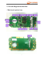
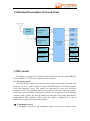
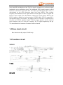
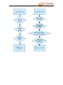
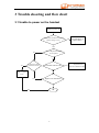
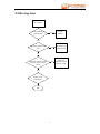
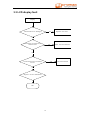
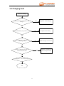
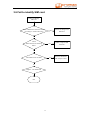
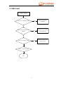
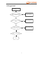
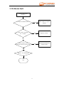
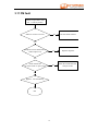
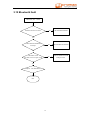
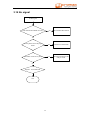
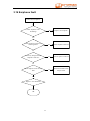
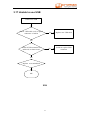
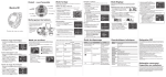
A27 Service Manual
1
Table of Contents
1. Circuit diagram instruction .................................................................................... 3
1.1 Main board explored view.............................................................................. 3
1.2 Detailed Description of Circuit Chart ........................................................... 4
1.3 RF circuit ......................................................................................................... 4
1.4 Base band circuit ............................................................................................. 5
1.5 Function circuit ............................................................................................... 5
2.Fault maintenance .................................................................................................. 6
3.Trouble shooting and flow chart ........................................................................... 8
3.1 Unable to power on the handset .................................................................... 8
3.2 No ring tone ..................................................................................................... 9
3.3 LCD display fault .......................................................................................... 10
3.4 Charging fault ............................................................................................... 11
3.5 Camera fault .................................................................................................. 12
3.6 Fail to identify SIM card .............................................................................. 13
3.7 MIC fault ....................................................................................................... 14
3.8 Keypad fault .................................................................................................. 15
3.9 Receiver fault ................................................................................................. 16
3.10 Vibrate fault ................................................................................................. 17
3.11 FM fault........................................................................................................ 18
3.12 Bluetooth fault ............................................................................................. 19
3.14 No signal....................................................................................................... 20
3.15 Failure to identify T-flash card .................................................................. 21
3.16 Earphone fault............................................................................................. 22
3.17 Unable to use USB....................................................................................... 23
2
1. Circuit diagram instruction
.1 Main board explored view
direction sensor
RF amplifier
receiving filter
四方向传感器
射频放大器
接收滤波器
FLASH
SC6820
T-card connector
Battery connector
RF transceiver
USB
26M crystal
connector
Earphone
connector
WIFI/BT IC
32.768
SIM connector
Crystal IC
LCD PAD
3
TP connector
1.2 Detailed Description of Circuit Chart
RF PA
(U112)
Rf
transceiver
U114
Rf
transceiver
U103
SIM card 1
Key pad
SIM card 2
Camera
BT/WIFI
T-card
1.3 RF circuit
This phone is designed on SC6820 platform. RF main chip integration SR1019,
PA use RDA6163A, TCXO uses 26MHz crystal oscillator.
(1) Receiving circuit
The GSM or DCS signal received from a base station via antenna is inputted from
the pin 27 of U101, send U104/U105 to pin A20/B20/A19/B19. This chip integrates
LNA and Frequency mixer. The signals are amplified by their own low-noise
amplifier (LNA). The amplified signal is sent to a down converter, where the signal is
mixed with local oscillation (LO) output from RX VCO to generate zero intermediate
frequency (ZIF) signals. The zero-IF signal passes through a filter and is amplified by
programmable gain amplifier (PGA), then the signal is outputted to I and Q
demodulator to generate I/Q base band signals.
(2) Transmitting circuit
A transmitter consists of I/Q modulation circuit, up-conversion mixer circuit,
4
power amplifier and duplex switch. The I/Q signal is inputted to be performed signal
modulation as the modulation signal. The modulated TXIF signals restrain its third
harmonic by harmonic suppression filter. The follow-up TXIF signal will be sent to a
discriminator on the offset frequency phase lock loop (OPLL). Then perform
frequency discrimination to this signal and the mixed signal of TXVCO signal and
RFVCO output signal. The discriminator outputs the signal control RFVCO and
RFVCO phase is enabled to lock at the phase of TXIF signal. TXVCO output RF is
still decided by RFVCO frequency. The phases of RFVCO and IFVCO signals lock at
the phase of VCTXO reference signal. TXVCO output signal is sent to emission
power amplifier (PA) A17/A16 pin to amplify. The TX signal outputted by PA pin
27is transmitted to the antenna via antenna switch to launch.
1.4 Base band circuit
Base band main chip adopts SC6820 chip.
1.5 Function circuit
WIFI/BT
T card
SIM card
5
Camera
2.Fault maintenance
Note:
The PCBA repairing is a very important work during the final production of cellular
phones. The speed and quality of repairing decides the yield and production efficiency.
The repair idea is very important for a good repairing technician. Make sure not to
heat a board right away once a phone reaches at hand.
6
7
3 Trouble shooting and flow chart
3.1 Unable to power on the handset
Failure to power on
Check battery mounted correctly &
battery voltage >3.4V?
No
Re-mount battery or
replace battery
Yes
Yes
Check if Keyboard backlight
can be lighted
No
No
Check if LCD is
connected correctly
Download software! Ok?
No
Solder or replace
LCD
Yes
Replace new mainboard
OK
Yes
8
Yes
Pay attention to
retain the calibration data
3.2 No ring tone
No ringtone
Check soldering of
speaker.OK?
No
Solder
speaker
Yes
Replace speaker and
test
Yes
OK! Mark the
failed speaker
No
Mark the
mainboard with
analysis result
No
Check the speaker circuit
no short ciruit or open
circuit
Yes
Replace new
mainboard
OK
9
3.3 LCD display fault
Abnormal LCD
Display
Check If the lcd is damaged
Yes
Replace new LCD
No
Check if the lcd connector is
soldered well
No
Solder the lcd connector
Yes
Check If the LCD is mounted
inverse
Yes
No
Replace the new mainboard
OK
10
Re-mount the lcd
3.4 Charging fault
Failure to Charge
Check charger or Replace new
charger
Yes
Replace new Charger
No
Check battery is good or not
No
Replace new battery
Yes
Solder charger connector
Yes
Check charger connector for
soldering defect
No
Check charging circuit of
mainboard for fault
Yes
No
Replace new mainboard
OK
11
Mark the mainboard
with analysis result
3.5 Camera fault
Failure to use camera
Check camera for damage
Yes
Replace new camera
No
Check if camera is soldered or
assembled well
Yes
Solder camera connector
or Re-assemble camera
No
Check camera circuit for fault
Yes
No
Replace new mainboard
OK
12
Mark the mainboard
with analysis result
3.6 Fail to identify SIM card
Failure to identify
SIM card
Check if SIM card is inserted correctly
According to insertion direction
No
Reinsert or change new
SIM card
No
Check
SIM connector for soldering
defect
Yes
Solder or replace SIM
connector
No
Check SIM circuit for fault
Yes
No
Replace new mainboard
OK
13
Mark the mainboard
with analysis result
3.7 MIC fault
Unable to record
No sound in microphone
Check mic for soldering defect
Yes
Solder or replace new
micphone
No
Check if mic sound hole is
jammed
Yes
Clean mic sound hole and
re-assemble mic
Yes
Mark the mainboard with
analysis result
No
Check mic circuit for fault
No
Replace new mainboard
OK
14
3.8 Keypad fault
Keypad doesn’t work
correctly
Check : DOME is pasted and
keymat is assembled correctly
Yes
Paste the DOME or
assemble keymat again
No
Is there any dirty on keypad
surface?
Yes
Clean keypad surface and
test
Yes
Solder or replace sidekey
No
Is sidekey soldered well?
No short circuit
No
Replace new mainboard
OK
15
3.9 Receiver fault
No voice in receiver
Is receiver ok ?
No broken wire
No
Replace new receiver
Yes
Check receiver connector for
soldering defect
Yes
Solder receiver connector
No
Check receiver circuit for any
fault
Yes
No
Replace new mainboard
OK
16
Mark the mainboard with
analysis result
3.10 Vibrate fault
Vibrator fault or No
vibration
Is vibrator soldered well ?
No
Solder vibrator or replace
vibrator
No
Check : Wire of vibrator
isn’t broken
Yes
Replace vibrator
No
Mark the mainboard with
analysis result
No
Check vibrator circuit
No short circuit or open circuit
Yes
Replace new mainboard
OK
17
3.11 FM fault
Failure to open FM or FM
can’t scan any station
Software version is correct
No
Re-download software
Yes
Earphone can be detected and
audio output is ok
No
Replace earphone
Yes
Check FM circuit
No short circuit or open circuit
No
Yes
Replace new mainboard
OK
18
Mark the mainboard with
analysis result
3.12 Bluetooth fault
Bluetooth can’t work
Software version is correct
No
Re-download software
Yes
Is BT antenna assembled
correctly?
No
Re-assemble BT antenna
No
Mark the mainboard with
analysis result
Yes
Check BT circuit
No short circuit or open circuit
Yes
Replace new mainboard
OK
19
3.14 No signal
No RF signal
Is RF antenna assembled correctly?
No
Re-assemble BT anntena
Yes
Is the phone set into Flying
mode?
Yes
Return to Normal mode
Yes
Mark the mainboard with
analysis result
No
Check RF circuit for any fault
No
Replace new mainboard
OK
20
3.15 Failure to identify T-flash card
Failure to read T-flash card
Is T-flash card inserted correctly?
No
Re-insert T-flash card
Yes
Check: the T-flash card is ok?
No
Replace new card
No
Clean socket or replace
socket
Yes
Mark the mainboard with
analysis result
Yes
Check card socket is clean and
no physical fault
Yes
Check card circuit for any fault
No
Replace new mainboard
OK
21
3.16 Earphone fault
Failure to use earphone
Check: earphone is ok?
No damage
No
Replace new earphone
Yes
Check earphone connector for
soldering defect
Yes
Solder earphone connector
Yes
Clean or replace connector
Yes
Mark the mainboard with
analysis result
No
Is there any foreign matter in
earphone connector?
No
Check earphone circuit for any
fault
No
Replace new mainboard
OK
22
3.17 Unable to use USB
Uable to use USB
Check : USB cable is ok, no pin of
connector is broken
No
Replace new USB cable
Yes
Check if USB connector is
solder ok, no short circuit
No
Yes
Replace new mainboard
OK
END
23
Solder or replace USB
connector