1
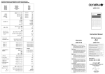
SERVICE MANUAL
PC-1280
SHARP
CODE: OOZPC1280SM/E
POCKET COMPUTER
MODEL
Pc-12ae
0
I
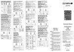
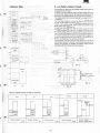
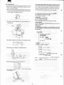
POCKET COMPUTER
.~I SP.!;,A y s I z E:
2 4* 2
PC-1280
j
-+--H--1t--LCD Screen
LINES
11-Pin
Connector""""'"'"""'..
~
~LCD Contrast
Dial
Iii================~~
fQ
1~
BS
@]
ms§~t:Jri:Jl§lrarnrn
l§J f!'\l
!ID ~ ITJ ~
l
RAM Slot
OH
[SJ
1"1$
--+-+=~'11-+H+-Cell
Compartment
imi:I
ffi!J llEI l!EJ
CfJ IE rID B
@ cD § ~ W
0[§][Q](f]l2J[ij]Q]@[QEJ
I
IT)
~[8](912][§]~[00r@J[QJ
[§] ~
ra
CT]
0
0
-
Memory
Backup
Cell
Compartment
Keyboard
c:J
OJ
Memory
Protect
Switch
(Internal
memory only)
Top View of PC-1280
Bottom View of PC-1280
1. INTRODUCTION
PC-1280 was designed to close with a tight fit to protect its LCD
screen and keyboard, and has the facility for double-precision
calculations.
2. Specifications
Model:
PC-1280 Pocket Computer
Processor:
8-bit CMOS CPU
Programming Language:
BASIC
System ROM:
136K Bytes
Memory Capacity:
System internal
1.6K Bytes Approx.
Data area .. .. .. .. .. .. .. .. .. .. .. .. . .. .. .. .. .. .. .. .. . .. . .. .. .. . .. .. .. .. .. .. .. . 208 Bytes
Program/Data Area
6558 Bytes
Reserve Area .. .. .. .. .. .. .. .. .. .. .. .. .. .. .. .. .. .. .. .. .. .. .. .. .. .. .. .. .. .. . 144 Bytes
(Memory expandable to 40KB using RAM cards)
Stack:
Sub-routine: 1 O stacks
Function: 16 stacks
FOR-NEXT: 5 stacks
Data: 8 stacks
Operators:
Addition, subtraction, multiplication, division, trigonometric, and
inverse trigonometric functions, logarithmic and exponential
functions, angle conversion, square and square root, sign,
absolute, integer, relational operators, logical operators etc.
Numeric Precision:
1 O digits (single-precision mode) I 20 digits (double-precision
mode) (mantissa) + 2 digits (exponent).
Editing Features:
Cursor left and right, line up and down, character insert, character
delete.
Memory Protection:
CMOS Battery backup.
Interface Capability:
11 pin (For cassette interface, disk, printer, etc.)
Ram Card Slot:
Cards of 2KB, 4KB, BKB, 16KB, or 32KB.
Display:
2-line 24-digit liquid crystal display with 5x7 dot characters.
Keys:
72 keys. Alphabetic, numeric, special symbols, and functions.
Numeric pad. User defined keys.
SHARP CORPORATION
-
PC-1280
Dimensions:
135(W) x 70.5(D) x 19.2(H)mm (closed)
5.31(W)x2.76(D)x0.76(H) inches
135(W)x141(D)x9.6(H) mm (open)
5.31 (W}x5.55(D)x0.38(H)
inches
Weight:
Approximately 180g (0.4 lbs.) (with cells)
Accessories:
Lithium cells (built in) and operation manual.
Options:
Plug-in RAM cards 2KB (CE-210M), 4KB (CE-211 M), 8KB
(CE-212M), 16KB (CE-2H16M), 32KB (CE-2H32M)
Cassette Tape Recorder (CE-152)
Printer/Cassette Interface (CE-126P)
Pocket Disk Drive (CE-140F).
Power Supply:
6.0V DC: Lithium cells.
type: CR-2032x2
Backup Battery:
Built-in memory backup cell.
type: CR-2032
Power Consumption:
6.0V DC @ 0.03W
Approximately 120 hours of continuous operation under normal
conditions (based on 1 O minutes of operation or program
execution and 50 minutes of display per hour at a temperature
of 20°C). The time may vary slightly depending on usage and
the type of battery used.
Operating Temperature:
0°-40°C (32°-140°F)
PC-1280
CE-124
CE-152
ea~~e~:1
••••••••••DOOCJ
••••••••••CJCJOCJ
••••••••-CICJCJCJ
········••CJCJO[:j
CE-126P
~:
CE-210M (2KB)
CE-211 M (4KB)
CE-212M (8KB)
CE-2H16M (16KB)
CE-2H32M {32k8)
CE-140F
3. Operating Battery Life and
Consumption Power
PC-1280 battery
Lithium battery:
CR-2032x2pcs
Capacity:
170mAH
10. Open the computer, switch on the power and look at the display.
If it looks like the following with an * displayed, Press the ALL
RESET button.
*
Terminal voltage:
6.0V
11. Turn OFF the power, remove the slot cover, and slide the
Memory Protect Switch to position A.
12. Replace the RAM card, if used.
13. Replace the slot cover and slide the switch back to the LOCK
position.
Consumption current
PC-1280 When OFF:
PC-1280When0N:
45µcA, max.
400µcA, max.
Replacing memory backup cell
The above is at the room temperature of 20°C and may vary
depending on conditions.
The memory backup cell in your PC-1280 has an effective life of
about five years under normal operating conditions.
ate that
temperature extremes can shorten cell life and cause memory
losses. When the memory backup cell was installed at the factory,
a label was attached above the memory protect switch, sho ·ng the
date of installation and a control code.
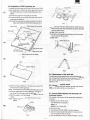
4. Battery Replacement
Replacing the operating cells
1. Turn the power OFF.
2. Close the computer and turn it over. Follow the diagrams on
the slot cover to remove the cover.
3. Remove the RAM card if present.
4. Slide the Memory Protect Switch to position B.
THIS IS IMPORTANT and must be done before removing the
operating cells or data and programs in memory will be lost.
Replacing Memory Backup Cell
DO NOT REPLACE THE MEMORY BACKUP CELL WHEN
OPERATING CELLS ARE REMOVED OR WEAK (mil
DISPLAYED WITH POWER ON): MEMORY CONTENTS WILL BE
LOST.
1. Turn OFF the power, close the computer and tum it over.
2. Remove the slot cover and RAM card if present
3. Slide the Memory Protect Switch to position B.
4. Release the screw (1) retaining the cover of the Backup Cell
compartment and remove the cover (2).
5. Replace the cell (3), making sure that the new cell is inserted
with the correct polarity (positive pole down).
6. Slide the Memory Protect Switch back to position A.
7. Replace the slot cover.
Replacing Operating Cells
5. Press the tab (1) and slide open the cell-compartment cover
(2). Remove the two lithium cells (3).
6. Replace the two cells, taking care that they are inserted with
the correct polarity, as shown in the diagram.
7. Replace the cell compartment cover (4).
8. Press the ALL RESET button.
THIS IS IMPORTANT AND MUST BE DONE TO PRESERVE
PROGRAMS AND DATA.
9. Replace the slot cover and slide the switch to the Lock position.
-2-
-
PC-1280
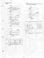
6. Low Battery Detect Circuit
5. Memory Map
Discussed next is about the low battery detect circuit which is
incorporated in the PC-1280.
As shown in the figure BELOW, when the input voltage VIN goes
above the detect voltage level VD, its output turns to high level. On
the contrary, when VIN goes below VD, the output turns to low level.
Two levels of caution and stop are detected by a single IC (LB iC
= MN1280).
The input voltage added to the input pin (No.2) is divided by R1
and R2, and R2 is turned on/off by the CAU signal of G.A. As shown
in Fig.3, when the supply voltage drops below the caution level, the
BATT symbol comes to activate. When it further drops down below
the stop level, the symbol goes out.
To sense the caution level, the CAU line of the G.A. is set active
(low) and the state on LB of the G.A. is checked. If LB is at a low,
the symbol activates. When the caution label is sensed, the CAU
line is set off (high impedance). With this, the voltage increases on
the LB iC pin 2 because there is no more voltage division by resistors,
so that the output changes from low to high level. As the LB line of
the G.A. is sensed again, the stop level is detected.
During standby, F01 of the CPU and CAU of the G.A. are set at
high impedance and Di 1 is inserted to correct the battery drop during
standby and operation. The ON/BRK and RESET switch became
inoperative after the stop level has been detected.
2800,~---DISP 1
2AO 0 .__
_
2
DISP
oo~o
2COO
-~----~
1
PC-1470U/75
PC-1280
POB
A13 sent
on POS
G.A. POS
selection
3ooo
Low battery
latch CE
3 2 o o Caution PON
latch write CE
2EOO
34
o o ROM bank CE
3600
3800
3AOO
3COO
3EOO
RAM bank
address
P05
Port write CE
P06
P07
Port write CE
~----P08
Memory map
POI
P02
P03
Key strobe
write CE
~----P04
4000
~--------->-03 02 nt
0
DO
0
0000
KS 1
0
Internal ROM,
KS8
KS1-KS8
SKB
CPU
2800
4000
Di 1
FOi
(P-Ch open)I-----___.
2000
RI
PISP & port
System ROM
I
1
'
16KBX8BANK
~
BANK RO
Rl
I
I
-
'I
R3
R2
I
I
I
Di 2
GA CAU -----'
R7
(N-ch open)
8000
Va;
AO 00
------
(Fig. 1]
(V)TIN
\'oM
\'oL
External
slot
Q)
~
2.0V
cooo ------
~ Sym - Caution label
0"----'----'--'----'-_,_4
-5: ·_bs>! P.N_ _
OUT
(V)
Stop level
c.
::>
rn
EOOO
(V)
Internal RAM,
-- SKB
SLT2
[Fig. 3]
Voltage detect IC operation
T
i
SLTl
[Fig. 2]
Memory mapping according to RAM card combination.
2K
4K
16 K
8K
32 K
800
Internal
RAM
000
cooo
D800
EOOO
FFFF
DOOO
SLOT 1
SLOT!
Internal
RAM
Internal
RAM
D800-FFFF
FFFF
lOK
DOOO-FFFF
SLOT!
sior i
SLOT!
Internal
FFF
12K
FFF
COOO-FFFF
-3-
16K
Internal
RAM
AOOO-FFFF
9FFF
FF
24K
8000-FFFF
8000-9FFF
40K
-
PC-1280
7. LSI Description
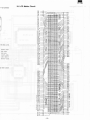
7-1. CPU {SC61860A38) signal description
Pin No
Signal
name
In/Out
1
2
3
4
5
6
7
8
9
10
11
12
13
A01
R/W
0AL
TES
01
00
RES
XIN
XON
XOUT
DIS
HA
IA8
Out
Out
Out
In
In
Out
In
In
In
Out
Out
Out
In/Out
I
I
I
20
21
22
23
24
25
26
27
28
29
30
31
32
IA1
IBB
IB7
IB6
IB5
IB4
IB3
IB2
IB1
VM
VA
GND
H1
In/Out
-
In
In
In
In
In
In
In
In
Out
I
I
I
45
46·47
48
49
50
51
52
53
H14
H15·H16
VB
VDIS
Out
vcc
voe
VGG
08
In
In
In
Out
In
In/Out
I
I
I
60
61
62
63
64
65
66
01
F05
F04
F03
F02
F01
BOB
In/Out
Out
Out
Out
Out
Out
I
I
I
73
74
B01
A08
Out
Out
I
I
I
80
A02
Out
Description (Standby = power off)
Address bus AO, high during standby
Write clock, normally high
Address latch. Clock used to latch the address of the LCD driver.
Test pin, normally low.
Oscillator input
Oscillator output
Reset input, reset with a high state of signal.
Cassette signal input
ON/BRK key input, normally pulled down to low level.
Cassette signal and buzzer signal output
LCD driver control signal, high during displaying.
LCD driver sync clock
Key input/key strobe
I
Key input/key strobe, low during standby.
Not used.
Not used.
Not used.
11-pin ACK (acknowledge on 11-pin interface)
11-pin DIN (data input on 11-pin interface)
11-pin DOUT (data output on 11-pin interface)
11-pin 102 (data input on 11-pin interface)
11-pin 101 (data input on 11-pin interface)
LCD drive power
LCD drive power
(+)supply
LCD backplate signal, 4-level pulse during displaying (1 /14 duty)
I
LCD backplate signal, 4 level pulse during displaying (1/14 duty)
Not used (because of 1 /14 duty)
LCD drive power, high during standby
LCD drive power, high during standby
LCD drive power, high during standby
LCD drive power, high during standby
(-)supply
Data bus, 07, normally high impedance
I
Data bus, DO, normally high impedance
Gate array chip enable (CE)
ROM chip enable
RAM card bank select (BA)
Not used.
Low battery detect, high impedanceduring standby.
Address bus A 15, high during standby.
(
Address bus A 1, high during standby.
-4-
~
-
PC-1280
7-2. Gate array (LZ92K38} signal description
Pin No
1
2
3
Signal
name
In/Out
BA
CE
DOO
In
In
In
I
I
I
6
7
8
9
10
11
12
13
14
15
16
17
18
19
20
21
22
23
24
25
26
27
28
29
30
31
32
33
D03
GND
P01
P02
P03
P04
P05
NC
SLTB
AS3B
AS1
AS2
AS3
AF15
AF16
SLT1
SLT2
DSP1
DSP2
RESO
KON
LB
RESI
BAK
VDD
GND
CAU
KS1
In
In
Out
Out
Out
Out
Out
Out
Out
Out
Out
Out
Out
Out
Out
Out
Out
Out
Out
Out
In
In
In
In
In
Out
Out
I
I
I
40
41
42
KS8
R/W
A9
Out
In
In
Description
Bank select
Chip enable
Data bus
I
Data bus
(-)supply
t t-pin 101 (P-channel open output)
11-pin 102 (P-channel open output)
11-pin DOUT (P-channelopen output)
11-pin DIN (P-channel open output)
11-pin BUSY (P-channel open output)
Not used.
Not used.
Not used.
System ROM 14 and RAM A 11
System ROM 15 and RAM A 12
System ROM 16 and RAM A 13
RAM card slot A 15
RAMcardA16
RAM card slot chip enable
Internal RAM chip enable
DISPCHIP1 chip enable
DISPCHIP2 chip enable
Reset output to CPU RESET line, normally low.
ON/BAK output to CPU KON line, normally low.
Low battery detect, low at battery low.
Reset input, normally pulled down.
ON/BAK key input, normally pulled down.
(+)supply
(-)supply
Low battery symbol activating voltage detect line, high impedance after the activation of the symbol.
Key strobe (P-channel open output)
I
Key strobe (P-channel open output)
Write clock
Address bus
I
I
I
I
48
A15
In
Address bus
-5-
-PC-1280
8. Service Precautions
2. Do the reverse sequence of the above to assemble.
NOTE: When removing CAB-A, be careful not to separate the static
tape.
Each cabinet is called as follows:
Display side bottom cabinet: CAB-A
Display side top cabinet: CAB-B
keyboard side bottom cabinet: CAB-C
Keyboard side top cabinet: CAB-D
8-2. Installationof CAB-C
*
*
CAB-A
Make sure that the pin is properly engaged into the hole.
When mating CAB-C to CAB-D, push CAB-C all the way in the
arrowhead A to achieve firm engagement. Tighten the screw with
the unit placed on the special table.
CAB-D
~J
li
8-1. Removal and installationof CAB-A
Procedure to mate CAB-A to CAB-B.
Latch
CAB-A
~[ [
Latch
I
@f~=:::::::::.::::=:::::::::.::::~-~=============~w
I
(Fig.1)
CAB-B
~
Pin in CAB-D (keyboard
side top cabinet)
CAB-C
Hole in CAB-C (keyboard side
bottom cabinet)
*The pin must be properly and firmly engaged into the hole.
8-3. Installationof the contactto the LOCK switch
knob
Latch B
* Two contacts may be attached to the knob, but it has to be installed
on the location shown in the figure. After installing the contact, it
has to be caulked to fix it secure.
I l
Contact
(Fig.2)
1.
Engage the latch A shown in Fig.2 in a manner as shown with
G) in Fig.1.
2. Engage the latch B shown in Fig.2.
3. Engage the latch C shown in Fig.2 in a manner as shown with
®in Fig.1.
Knob
Procedure to remove CAB-A
1.
As shown in the figure, insert your nail in a clearance between
CAB-A and CAB-C and push it in the arrow direction to disengage
the latch C (Fig.2) at two locations. CAB-C must be disengaged
first to achieve easier removal.
-6-
-
PC-1280
8-4. Installation
of PWB, keysheet, etc.
Buzzer leads
G) Assemble the blind sheet and the main PWB unit onto CAB-B.
® Insert rubber keys in CAB-D, then insert upper half of the key
sheet. Match the guide pins and key sheet holding pins in their
CAB-A
A
Black
positions.
@ Match the key spacer with the guide pin and insert.
© Fold back the lower half of the key sheet and insert only the
terminal onto the guide pin.
NOTE: Leave the lower side key sheet uninserted onto CAB-D
guide pin and holding pin and the folded area loose (Fig.1 ).
Red
(Fig.4)
CAB-B (display side top cabinet)
Main PWB unit
®
Bring the display side bottom cabinet (CAB-A). Solder the buzzer
leads first (Fig.4) and fasten the terminal lug of the static tape
using two tapping screw.
@ Mate CAB-A with CAB-B.
® Close the unit halfway and mount the lower half of the key sheet
and the memory PWB on CAB-D.
@ Mate CAB-C.
Blind sheet
(Fig.5)
CAB-D (keyboard side top cabinet)
(Fig.1)
FPC
Memory PWB unit
(Fig.6)
8-5. Replacement of the static tape
The static tape must be replaced with a new one once after it has
been removed from the aluminum panel. Wipe away residual glue
after bonding. Check ground continuity after the installation, in
reference to 8-6.
(Fig.2)
8-6. Ground continuitycheck
®
Mount the memory PWB unit in Fig.2 and insert only the FPC
terminal onto the CAB-B guide pin.
NOTE: Do not insert the memory PWB onto the CAB-D guide pin yet.
@ Insert the mask sheet and fixing rubber (Fig.3) and fold back a
part of the FPC and insert it onto the CAB-B guide pin.
Make sure that the resistance between the display side cosmetic
panel and the RAM card lid is not more than 50.
8-7. Internal RAM capacity and auto-power off
functionalchecks
CV
Match the angle to the CAB-B guide pin and fasten it with four
screws.
NOTE: Tighten two screws in the center first, then two more
adjacent to it.
-:
The contents of the memory will be erased after the following is
conducted.
(j) Depress the ALL RESET switch.
The following will be displayed.
MEM$="2"
Guide pin
®
®
©
®
(Fig.3)
-7-
MEMORY ALL CLEAR OK?
Push the [Y] key.
Type [M) and [ENTER]. "6558" will come displayed.
Leave it in the above state for more than 14 minutes, then make
sure that power has been turned off.
Push the [ON] key to bring the display message in ® above.
T
-
PC-1280
8-8. Precautions
8-9. Display side cabinet and keyboard side cabinet
• All components must be closely attached to the PWB and soldered.
•When the LSI is replaced, use KR19RAM to solder with (see
Service Information PS-009).
• The 0.1 µ.F ceramic capacitor (RC-KZ1054CCZZ) inserted across
the KON pin of GA (pin 26) and the VGG side of the 0.033µ.F
must be handled in the following manner:
The above two cabinets are mated together with the spring pin in
use. To replace one of the cabinets, it is possible to remove the
spring pin by scraping off the cabinet body using such as wire cutter,
but the spring pin once removed may not be used again.
9. Check-Out with the Test Program
A test program is contained in the ROM.
•Check item
(1) RAM card read after
(2) 11-pin connector 1/0
(3) 15-pin connector 1/0
NOTE: The above item
• The capacitor must be inserted to the 11-pin connector in the
following manner:
write test
line tests
line tests
(3) is not used by the PC-1280.
• Tools required
The PC-1360 special tool UKOGC3020CSZZ (price rank: BC) is
used for (2) and (3).
• Description
The RAM contents must be saved on such as tape before conducting
the above test item (1 ), because the program and data are destroyed
during the test.
OFF)
(Power
Turn power on with the following
four keys depressed
at the same time.
···~GIJIE]IQI
PC-1280···
• The resistor (1 OOkll) must be inserted in the following manner:
PC-1475
J···!2J ~
I
(MENU)
I I:RAM
ITl[B]
2:11PIN
3:15PIN
Type [I)
• The diode must be inserted in the following manner:
(I)
RAM test
(2)
11-pin check
Type [2J
Type [ID
(3)
23
POWER switch
~----•(Power
28
__
Tu_be_2_7
.,
NOTE-2:
• See the table below for the size of jumper wire.
Size
140
J2
40
J3
105
• The capacitor (RC-K1E104HCZZ)
in the following manner:
OFF)
•1
NOTE-1:
J1
15-pin check
(Not necessary for the PC-1280)
x 2 pieces must be inserted
-8-
Power can be turned off while the above message is on
display.
If the test program fails to start, check keys first.
• Details of check items
(1) RAM test
(2) t t-pin test
Set the t t-pin connector of the test tool with the t t-pin connector
of the unit with the parts side facing up.
Menu
Menu
[I]
<RAMl)
B:4K
D:l6K
A:2K
C:SK
E:32K
IA], [BJ, ~.
<llPIN)
XWAITX
P:PASS
[DJ, IE]
<RAMl)
XWAITX
IENTERI
<llPIN)
XOUT:HIGH
XIN:LOW
IENTERI
<RAMl)
ERROR OCCURED AT ????H
<llPIN)
CHECKED
JENTERJ
<RAMl)
(????H-????H
Menu
IS CHECHED)
!ENTER!
<RAM2)
A=2K
NOTE-1:
B:4K
C:SK
IA],
D:l6K
E:32K
rm
l!2J•
~.
[DJ,
See the following for the sequence of the test vs. the
test pin.
P:PASS
See
Ip
IE] NOTE-3.
<RAM2)
CD
®
®
XOUT->XIN
101->102
©
DOUT->DIN
DIN->DOUT
BUSY-.ACK
®
®
102->101
IENTERI
<RAM2)
ERROR OCCURED
Specialtesltool11-pinoonnector
sidecircuil diagram
AT ????H
NOTE-2:
<RAM2)
(????H -????H
I ENTER
IS CHECKED)
I
Menu
OTE-3:
OTE-4:
The RAM corresponds to the slot in the following way.
PC1280
PC1475
RAM1
SLOT
SLOT1
RAM2
8KB internal RAM
SLOT2
The contents of the RAM are destroyed during the test.
To preserve the RAM contents, type the [Pl key to pass
the test.
-9-
Error will not be caused, if signal lines were to short
within the unit.
..
PC-1280
10. LCD Matrix Circuit
' 11-pin connector
H4
H5
HS
H7
,f the test vs. the
XOUT-.XIN
101-102
102-101
DOUT-.DIN
DIN-.DOUT
BUSY-.ACK
ss were to short
-10-
-
PC-1280
11. Circuit Diagram
1) The resistor with no comment is 1/aW, J (±5%)
2) The capacitor with no comment is 25WV, (F)
Hl-7
L
--..
LF-7318E
5
l
r rr r r r
l ll
•
'--lE
'--
.
54'!
~~
'--jj
'-''-
SC43536
SISO
'-t:ffi
St52
'-I
I'-
-~1=
7 l--
~t!ti
r-- see
H~
r:::~
see
'-W!
l~=N
03
VeAT
I~
111~
'V
1
.• CR2032
Sil
>->-1---'
..J"""l'i"'I
·~
• fil--'
::::~
...__~
-oo
1=
-rv
~
_,
SC43536
~~
_,
_,
r-- ss
J......,
~~
s •>--
I'-~
RESET
6~
COISP2)
r--;m
CIO
820P(L)
VRI
205.
_,
::::~
.......
·~-N
I)
RIS
vv
1001(.
,~
I
-
04
ISRl48
c,,',!!· 1 "rl I-
A A A
vv
Rl5
IM
wr
<:»
~
3
E1
~~
~~
VGG
I
r r
Gi5L
-
lC9150PCHl
~~"'
!
§I
LH5310X7
CROM) e
Id
Rl4
E'~'ll'll::l---·
l
IM
"
'--
KSI
A/W
A •
~1
;--
i=
<r-
v-
r-:lli
=~=l"J
l
LZ92K38
14
I
05133
L-
9 T
st. Tl
...
AFI
AS3
~91~
12
,--
MN
1280
I
II
,.--
~a 1 a
-
f'-fHl
f'-.
,...___~
~E:
~~
02
fG~~,A~ c~1~8
'Cl
IJ_!!: ~i
~~~~
~
SLOT
IOK
I I
r
I~~~~~~~
8K
04364
Rt7
T3~~
~
_._.
ca a.o3.s-cei
' - J"""l'i"'I
J
T
SW
If--
>-1--
..L
I
J
r>.
'.:::.J
rr-.
_,
r rr r
I
.,
s ........
'--i:IB
s
'-
OAN202
~--'
I
I
•I-s >--
COISPI)
'-- ee
--
CL CO)
10 .......
'-- s •
H8-14
CG. A)
•
~
""J! ~~
I
GNO..l
Vee
R/'11'
A 0 '----'
-
---------_---_
----
2
A I
A 2
A 3
A 4
A 5
A 6 _,
A 7 _,
A 8
A 9 >---'
AIO
AI I
Al2
Al3
Al4 ..............
Al5
Al6
NC >NC ......
D 0 L-0 I
D 2~
D 3~
D 4
D 5
D 6 L-D 7~
CE
NC
NC
OE h
OT
.___..,
.___..,
._____,
Vw
A
35
~
Internal
lOOK!l
>
Y4 w
r
RAM Protect
A:SHORT
B:OPEN
c
8
-11-
SW
D
E
I
GNO
•CAL
VA
H8-14
_l
CR2032*2
VM
VG
VAi
T=1-
5
20K
5
3.3~
VB
¥
VDIS
O.lµF
RI
JO
X2
FG
01
RESET SW
ca
OAN202
GG
o , 03s. <ai
RIS
1001(.
4
IA6
09
IA7
IA71
SW
!AS
LOCK:QPEN
R7
J:OPEN
EX:SHORT
I 001<
3
KS8
C5
A38
C6100,cH)
IOOP
CH)
XI CSB768
RB
CCPU)
IM
~mff ~~TII___.
QI
2
A I I
OT4
JOOK
OTC 144
F.G
.o rz
05
!!Pin
MT2
GNO
OA204K
,------..,
I
r-+*l-'-+-++-+-~~--,.""1(/rr-=::;-::-~~
:
Va;
:OT3
Cl2
I
Cl3
BUSY
OOUT
XIH
XOUT
01•
ACK
102
101
E
F
G
-12-
- H
12. Parts & Signal Description
Main PWB bottom side
j
Memory PWB bottom side
-13-
-
PC-1280
Main PWB upper side
{1 .2mm heigt MAX)
Memory PWB upper side
No foil pattern
-14-
-
PC-1280
13. PARTS LIST & GUIDE
IT] Exteriors(~~)
NO.
1
2
3
4
7
8
9
10
11
12
13
14.
15
16
17
18
19
20
21
22
23
24
25
26
27
28
29
30
31
32
33
34
35
36
37
38
39
40
41
42
43
44
45
46
101
102
103
PARTS CODE
DUNTG1226ECZZ
DUNTG1229ECZZ
PFiLW1009ECZZ
PSHEZ 1019ECZZ
DUNTK1227ECZZ
PGUMS 10 l 7ECZZ
CPWBF1052EC01
QCNCW1306CC1B
LX-BZ l 155CCZZ
RALMB1030CCZZ
PTPEH1213CCZZ
PTPEH1026ECZZ
DUNT-1230ECZZ
PGUMM1015ECZZ
LANGT 1011 ECZZ
LX-BZ1200CCZZ
DUNTG1268ECZZ
GFTAS1282CC01
DUNTG1225ECZZ
DUNTG1228ECZZ
LPiNS1002ECZZ
PGUMM1013ECZZ
PGUMM1013ECSA
PZETL1024ECZZ
C p\JiB F 1053EC0
1
MSPRClOllECZZ
MSPRClOOlECZZ
QCNTM1042CCZZ
MSLiP1003ECZZ
PGUMM1594CCZZ
PGUMS1608CCZZ
PZETL1564CCZZ
QTANZ1503CCZZ
QCNTM1056CC01
JKNBZ1747CCZZ
GCABA1030ECZZ
QTANZ1504CCZZ
LFiX-1190CCSC
TLABHl 127ECZZ
TLABH1143ECZZ
GFTAU1012ECZZ
QTANZ1406CCZZ
LX-BZ1018ECZZ
LX-BZ1147CCZZ
LX-BZ l l l 6CCN 1
PSPAPlOOlECZZ
TLABH1160ECZZ
TLABH1161ECZZ
PZETL1029ECZZ
TLABZ1008ECZZ
TLABS1078ECZZ
TLABH1956CCZZ
PRICE RANK NEW PART
Ex
Ja MARK RANK
EM
N
0 Oisolav cabinet unit (TOD)
AP
N
0 Display cabinet unit (Too)
AD OF
N
c Polarized filter
AB DC
N
c Mask sheet
EV
FM
N
B
LCD unit
AB DC
N
c Rubber connector
BS
NF
N
E
Main PWB unit
AK DY
c Connector 0 2Din)
AA
DA
c Screw (2X8)
AD OF
B
Buzzer
AB
DB
c Taoe
AE 0 J
N
c static tape
AK DY
N
B
Key sheet
AB DC
N
c Fixin2 rubber
AC
DE
N
c Fixin2 anzle
AA DA
c Screw
AP
EM
N
0 Displav cabinet unit (Bottom)
AB OB
0 Connector cover
N
EM
0 Key cabinet unit (ToD)
AP
N
0 Key cabinet unit (ToD)
AA DA
N
c Sorina oin
N
B
Kev rubber
EC
N
Al
c Kev rubber
AA
DA
N
c Kev soacer
AX FU
N
Memory PWB unit
E
AA DA
N
c Earth sl)ring
AB DB
c PS sorinz for RAM card
AA DA
c Slide switch terminal
AB
DC
N
c Slide switch knob
AB DB
c Reset soring rubber
AE 0 J
c Rubber connector for RAM card
AB
DC
c Insulator sheet
AB OB
c Battery terminal A
AA DA
c Contact for slide switch
AA OB
c PS switch knob
AE DK
N
0 Kev cabinet unit (Bottom)
AB DB
c Batterv terminal B
AB DC
N
c Card stcooer
N
DA
c Battery caution label
AA
N
c Battery caution label
N
0 Lid for card
AE OM
AB DC
c Battery terminal (tf1iS;l
AA DA
c Screw
AA DA
c Screw 12 X 4.5)
AA DA
c Screw
AA DA
c Reset spacer
DA
N
c Caution label(Battery replacement)
AA
N
c Caution label(Battery reptacernent)
AB DB
c Insulator sheet
N
AA DA
c Caution label
0 VCCI label 3
DA
AB DB
c Protector label
-15-
DESCRIPTION
* ., rr
(Jaoan) t 3 '7/~1" t";t. .,
(exceot Jaoan) t 3 '7;; ~ 1" t"
"/:J'7711i.-'1;I] 7:,,-;,.- r
LCDi=- ., r
::J°J.,,::J;t.7'!
(Include No.9) J1 ;_,~,<;, i=...,
::J;t.7'1t" ;z
i=- .,
i=--,
r
r
r
1-tf"'/;t/'11
-t1T'/'i-l
::J'i1'i-l
~-/-r
7 ::J"J.,,
7-,+1"
7 ., + 1" 7 7 / 7" '"
t" ;z
3 " ;; ~ 1" c t· ., r i.:: .. , r
::J;t.7'1- 7'!
(Japan) ~-~ 1" t• ;t. ., r ice .. , r
(except Japan) ~ - ~-\" t" ;t. ., r ice .. , r
A /IJ / 7°C/
(Japan) :J" J.,, ~ lexceotJaoan) :J"J.,,~~-;z-.:--ijJ-f:IJ-~'</ i-·' r
-t1'f";, ;z/1J ;,7
RAM;IJ- r· 3 '7 PS:Z /1J ;..- 7"
;z 7 1 r· ;z 1 ., + 3 ,,_, -t ., -i- ;..:z 7 1 r· :z 1 ., + ·1-.... :
IJ -j: ., r A/ 1) / 7° ::J" J.,,
RAM;IJ-r3'7
::J"J.,,::J;t.77-t"·1 .r, / ;,.- r
''·'T'!-'I>/
A
;z 7 1 r x 1 ., + 3 '7 -t ., 'i ;..PS:z 1 ., + '/< c
~ - ~ 1" t:
r i =- ., r
'' ., T 'J - 'I / / B
t
* .,
;I]-
1:
J..
r ., ,,_
(Japan) 7;,++1'71
7-.:1i.(exceot Jaoan) T/ ++ i '71 7-.:1i.;I]-
r·17
, '., T ') - 'I ;..- ;,
t" ;z
t" ;z
t" z:
1) -t I r ;z-.:--ij-(Japan) T/ + :J '7 ;I]/ + 1 '71
(except Japan) T/ + :J '7 ;I]/ + .1 '71
'71 7-';/r+1 '717-.:1i.(Japan! VCCl7"''" 3
.1'/'7/
;j;:J" 7-.:1i.-
7-.:1i.7-.:1i.-
22
-----~:
25
44
38
-16-
-
PC-1280
[£] Main PWB unit(.;< 1 /£t.&i=
NO.
PARTS CODE
I
2
3
4
5
6
7
8
9
10
11
12
13
14
15
16
17
18
19
20
21
22
23
24
25
26
27
28
29
30
31
32
33
34
35
36
QCNCW1306CCIB
RC-CZD105ECZZ
RC-CZ1047CCZZ
RC-EZ335BECOJ
RC-KZ1054CCZZ
RC-ZZI006CCZZ
RCRSZ1063CCZZ
RH-OZIOO!ECNI
RVR-Z2400QCZZ
VCCCTPIHHIOIJ
VCCCTPIHH151J
VCKYTPIEF!04Z
VCKYTPIHB82 IK
VHDDAN202K/-l
VHDDA204K//-l
VHDDSS133//-l
VHiD4364Gl5LN
VHiLH5310X7-l
VHiLZ92K38/-l
VHiMN1280Q/-l
VHiSC43536/-l
VHiSC61860A38
VRS-TP2BD100J
VRS-TP2BDI03J
VRS-TP2BDI04J
VRS-TP2BDI05J
VRS-TP2BD203J
VRS-TP2BD393G
VRS-TP2BD472J
VRS-TP2BD562G
VRS-TP2BD563J
VSDTA144EK/-l
VS D TC I 4 4E K/- I
VS2SC2412K/-l
RC-K1El04HCZZ
VRD-HT2EY104J
1-•;J r (Unit)
901 CPWBF!052ECOI
''J
l)
PRICE RANK NEW PART
Ex
Ja MARK RANK
AK DY
c Connector ( 11 oi n )
AC DD
c Capacitor (luF)
AB DB
c Capacitor (0 033uF)
AB DC
c Caoacitor (6.3WV 3.3uF)
AB DC
c Capacitor (50WV O. luF)
AB DB
c Caoacitor (0.1 uF)
a Crvstal (768KHz)
AF OM
B
AD OF
Diode OSR14S)
AF ON
B Variable resistor (20K(l)
AA DA
c Caoacitor (50WV IOOPF)
AA DA
N
c Caoacitor (50WV l 50PF)
AA DA
c Capacitor (25WV O.!OuF)
AA DA
N
c Caoacitor (50WV S20PF)
AB DB
B
Diode (DAN202K)
B
AC DC
Diode (DA204K)
B
AA DA
Diode ross 133)
BO GU
B
IC (D4364Gl5LN)
B
AW FR
IC (LH5310X7)
B
AN EK
IC (LZ92K3Sl
IC (MN l 2S00)
AE DH
B
B IC (SC43536)
AX FU
B
AX FU
IC (SC6IS60A3S)
AA DA
c Resistor (l/SW 100 ±5%)
AA DA
c Resistor (l/SW !OKO ±5%)
AA DA
c Resistor (I/SW IOOKO ±5%)
AA DA
c Resistor (I /SW I.OMO ± 5%)
AA DA
c Resistor <l/SW 20KO ±5%)
AA DA
c Resistor (I/SW 39KO ±2%)
AA DA
c Resistor (I/SW 4.7KO ±5%)
AA DA
c Resistor (I/SW 5.6KO ±2%)
AA DA
c Resistor (l/SW 56KO ±5%)
B Transistor <DTA!44EKl
AC DC
B Transistor <DTC144EK)
AC DC
B Transistor (SC24 l 2K)
AB DB
AB DC
c Capacitor(25WV 0.JµF)
AA DA
c Resistor (l/4W lOOKD +5%)
BS
NF
N
E
PARTS CODE
I
LPLTPI007ECZZ
TiNSJl!l8ECZZ
TiNSE1122ECZZ
TiNSG1123ECZZ
SPAKC0276ECZZ
SPAKC0279ECZZ
TLSTSI015CCZZ
SPAKA0278ECZZ
PHOG-1001ECZZ
2
3
4
5
6
:.if.1:5':.i;,-f·:.--t:J/f"/-tf--
:.i;,-f·:.---t:.i:.--7:.---t:J/T/"t-
11)
;;(.)'Iv
Y 1 ot- i:
n i:
:.i:.--7"·:.--tt:.i:.--7:.--t-
j:IJ
::i:.---T·:.---tt:J/'}-°/ij"-
Y1 ;tY1 ;t-
r·
f'
Y1ot-r·
IC
IC
IC
IC
IC
IC
T1
-f 1
-f 1
::i "l
::i '7
::i '7
T.{ ::J </
-f 1
::i '7
-T1 ::i '7
-f 1 01 '7
-f 1 :.i '7
-f 1 01 '7
f 7/'/;;(.:5'r7/'/;;(.:5'f7:.--'/;;(.:5':J/7°/-t71 :J '7
) 1 / "',
Main PWB unit
[JJ Packing material & Accessories(.ml~
NO.
DESCRIPTION
</
::L-- ·1
f
c 1t~J1)
PRICE RANK NEW PART
Ex
Ja MARK RANK
AC DD
N
D Temolate
F X
N
D Instruction book
AX
N
D Instruction book
AX
N
D Instruction book
ON
N
D Packing case
AF
N
D Packing case
DA
D Service list
AD OF
N
D Packinz cushion for set
AA DA
D Pr o t ec to r sheet
N
-17-
DESCRIPTION
-f/7'v-f
(Japan) r ') 7 "/ fJ 1 -t '/ ) 1 3
(except Japan.Germany) r IJ 7 '/ 7J 1 -t '/ ) 1 3
(Germanv) r 1) 7'/fJ1-t'/)1
3
(Jaoanl """°/:7'7-;;(.
(exceot Jaoan) ''""'/:7'7-;;(.
(Jaoan) 't-1:' ;;(. '! ;;(. f
-t '/ f 3 '7 , { ·1 "' / ::r :; ·1
:1'}
'7 ::;>;t::i'J:,.--;;<,
;,.
3 /
-
PC-1280
SHARP
COPYRIGHT
©
1987 BY SHARP CORPORATION
All rights reserved.
Printed in Japan.
No part of this publication may be reproduced,
stored in a retrieval system, or transmitted,
in any form or by any means,
electronic, mechanical, photocopying, recording, or otherwise,
without prior written permission of the publisher.
SHARP CORPORATION
Information Systems Group
Quality & Reliability Control Center
Yamatokoriyama, Nara 639-11, Japan
1987 March Printed
in Japan
®


![取扱説明書〈詳細版〉 [F-01B]](http://vs1.manualzilla.com/store/data/006609204_2-ba82d04dd0f6be34caac6e011e0e94c5-150x150.png)