1
-
PC-1280
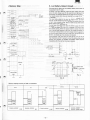
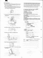
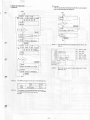
6. Low Battery Detect Circuit
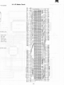
5. Memory Map
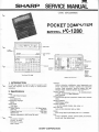
Discussed next is about the low battery detect circuit which is
incorporated in the PC-1280.
As shown in the figure BELOW, when the input voltage VIN goes
above the detect voltage level VD, its output turns to high level. On
the contrary, when VIN goes below VD, the output turns to low level.
Two levels of caution and stop are detected by a single IC (LB iC
= MN1280).
The input voltage added to the input pin (No.2) is divided by R1
and R2, and R2 is turned on/off by the CAU signal of G.A. As shown
in Fig.3, when the supply voltage drops below the caution level, the
BATT symbol comes to activate. When it further drops down below
the stop level, the symbol goes out.
To sense the caution level, the CAU line of the G.A. is set active
(low) and the state on LB of the G.A. is checked. If LB is at a low,
the symbol activates. When the caution label is sensed, the CAU
line is set off (high impedance). With this, the voltage increases on
the LB iC pin 2 because there is no more voltage division by resistors,
so that the output changes from low to high level. As the LB line of
the G.A. is sensed again, the stop level is detected.
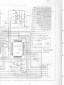
During standby, F01 of the CPU and CAU of the G.A. are set at
high impedance and Di 1 is inserted to correct the battery drop during
standby and operation. The ON/BRK and RESET switch became
inoperative after the stop level has been detected.
2800,~---DISP 1
2AO 0 .__
_
2
DISP
oo~o
2COO
-~----~
1
PC-1470U/75
PC-1280
POB
A13 sent
on POS
G.A. POS
selection
3ooo
Low battery
latch CE
3 2 o o Caution PON
latch write CE
2EOO
34
o o ROM bank CE
3600
3800
3AOO
3COO
3EOO
RAM bank
address
P05
Port write CE
P06
P07
Port write CE
~----P08
Memory map
POI
P02
P03
Key strobe
write CE
~----P04
4000
~--------->-03 02 nt
0
DO
0
0000
KS 1
0
Internal ROM,
KS8
KS1-KS8
SKB
CPU
2800
4000
Di 1
FOi
(P-Ch open)I-----___.
2000
RI
PISP & port
System ROM
I
1
'
16KBX8BANK
~
BANK RO
Rl
I
I
-
'I
R3
R2
I
I
I
Di 2
GA CAU -----'
R7
(N-ch open)
8000
Va;
AO 00
------
(Fig. 1]
(V)TIN
\'oM
\'oL
External
slot
Q)
~
2.0V
cooo ------
~ Sym - Caution label
0"----'----'--'----'-_,_4
-5: ·_bs>! P.N_ _
OUT
(V)
Stop level
c.
::>
rn
EOOO
(V)
Internal RAM,
-- SKB
SLT2
[Fig. 3]
Voltage detect IC operation
T
i
SLTl
[Fig. 2]
Memory mapping according to RAM card combination.
2K
4K
16 K
8K
32 K
800
Internal
RAM
000
cooo
D800
EOOO
FFFF
DOOO
SLOT 1
SLOT!
Internal
RAM
Internal
RAM
D800-FFFF
FFFF
lOK
DOOO-FFFF
SLOT!
sior i
SLOT!
Internal
FFF
12K
FFF
COOO-FFFF
-3-
16K
Internal
RAM
AOOO-FFFF
9FFF
FF
24K
8000-FFFF
8000-9FFF
40K