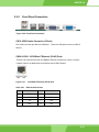
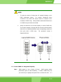
1
WAFER-LX
3.5” Profile WAFER Embedded Board
User Manual
RoHS Compliant
WAFER-LX
Revision History
Title
3.5” Profile WAFER-LX Embedded Board
Revision Number
Description
Date of Issue
1.0
Initial release
April, 2006
Copyright Notice
The information in this document is subject to change without prior notice in order to improve
reliability, design, and function and does not represent a commitment on the part of the
manufacturer.
In no event will the manufacturer be liable for direct, indirect, special, incidental, or consequential
damages arising out of the use or inability to use the product or documentation, even if advised of
the possibility of such damages.
This document contains proprietary information protected by copyright. All rights are reserved. No
part of this manual may be reproduced by any mechanical, electronic, or other means in any form
without prior written permission of the manufacturer.
Trademarks
AMD is the registered trademarks of Advanced Micro Devices, Inc. Geode, GeodeLink, Virtual
System Architecture and 3DNow! are also trademarks of Advanced Micro Devices, Inc. AMI is a
registered trademark of American Megatrends Inc. Other product names mentioned herein are
used for identification purposes only and may be trademarks and/or registered trademarks of their
respective owners.
Page 22
Page
IEI® Technology, Corp.
WAFER-LX User Manual
Table of Contents
Revision History ·························································································································· 2
Copyright Notice ·························································································································· 2
Trademarks··································································································································· 2
Table of Contents ························································································································· 3
List of Tables ································································································································ 6
List of Figures ······························································································································ 7
Product Overview ·····················································································································1-2
CHAPTER ONE
1.1
INTRODUCTION
General Information ········································································································1-2
Connectivity ····························································································································1-4
Label
··································································································································· 1-4
Function ·································································································································· 1-4
1.2
WAFER-LX Board Overview ··························································································· 1-8
1.3
Technical Specifications ································································································ 1-9
Audio Connector ···················································································································1-10
AC ’97 interface ···················································································································· 1-11
Packing List ······························································································································ 1-11
System Monitoring ···················································································································· 1-11
CHAPTER TWO FUNCTIONAL DESCRIPTION
2.1
CPU, Memory, and Chipsets
··················································································· 2-2
CPU ············································································································································ 2-2
Memory ······································································································································· 2-3
VGA/LCD Interface ····················································································································· 2-3
Audio ·········································································································································· 2-3
Block Diagram···························································································································2-4
Important Features ···················································································································2-5
2.2
External Interfaces ··········································································································2-7
Page 3
WAFER-LX
2.2.1 Internal Connectors ······································································································ 2-11
2.2.2 Front Panel Connectors ·······························································································2-31
CHAPTER THREE
3.1
INSTALLATION
Considerations Prior to Installation ·············································································· 3-2
Preparing Your Embedded Board ······························································································· 3-2
Installation Notices ······················································································································ 3-2
Airflow Consideration ··············································································································3-3
Unpacking Precautions ············································································································3-3
Memory Module ························································································································3-3
3.2
Mechanical Diagrams ····································································································· 3-4
3.3
Jumper Settings ··············································································································3-5
JP1 (AT/ATX Mode Selector) ································································································· 3-6
JP1 Pin Configuration·············································································································3-6
JP1
··································································································································· 3-6
JP2: COM3 Serial Port Operation Mode Selector ·································································· 3-6
JP3: COM Ports Power Selector ···························································································· 3-7
3.4
Installation ·······················································································································3-8
IDE Disk Drive and CDROM Connector ················································································· 3-8
Optional Floppy Drive Connector (CN31) ·············································································· 3-9
Compact Flash Disk ···············································································································3-9
Parallel Port Connector (CN15)······························································································ 3-9
Audio Interface ·····················································································································3-10
COM Port Connectors [COM1(CN22), COM2/COM3(CN16)] ············································· 3-10
LCD Panel Connection (CN26, CN28, and CN29) ······························································ 3-10
Ethernet Connection (CN20 & CN21) ·················································································· 3-11
USB Connection (CN24 and CN19) ·····················································································3-12
Accessories Included in Kit ···································································································3-12
Type
································································································································· 3-12
CHAPTER FOUR
AWARD BIOS SETUP
Introduction ·······························································································································4-2
Page 44
Page
IEI® Technology, Corp.
WAFER-LX User Manual
1.1.1
Starting Setup ············································································································4-2
1.1.2
Using Setup ···············································································································4-2
1.1.3
Getting Help ··············································································································4-3
1.1.4
Unable to Reboot After Configuration Changes ························································ 4-3
1.1.5
Main BIOS Menu ······································································································· 4-3
Standard CMOS Features ········································································································4-5
1.1.6
IDE Channel Master ·································································································· 4-8
Advanced BIOS Features ·······································································································4-10
1.1.7
CPU Feature ···········································································································4-17
1.1.8
Hard Disk Boot Priority ····························································································4-19
Advanced Chipset Features ··································································································4-20
Integrated Peripherals ············································································································4-26
1.1.9
OnChip IDE Device ·································································································4-27
Power Management Setup ·····································································································4-31
1.1.10 Onboard Device ······································································································4-37
1.1.11 Super I/O Device ·····································································································4-39
PnP/PCI Configurations ·········································································································4-44
PC Health Status ·····················································································································4-47
Frequency/Voltage ··················································································································4-49
APPENDIX A WATCHDOG TIMER
APPENDIX B
CONNECTING ATX POWER
Power Supply ··························································································································· B-1
1.
Using ATX Power Switch ································································································ B-2
2.
Using AT Power Supply ·································································································· B-3
APPENDIX C
ALI® RAID FOR SATA
1. Introduction ·························································································································· C-2
Precautions:··························································································································· C-2
2. Features and Benefits ······································································································· C-3
3. SATA-ALi RAID Driver ··········································································································· C-4
Page 5
WAFER-LX
4. Accessing the ALi RAID Utility ··························································································· C-6
Safety Notice ································································································································ 8
ESD Precautions ·························································································································· 8
Conventions Used in This Manual ····························································································· 9
Software Updates························································································································· 9
List of Tables
Page 66
Page
Table 1-1
Models with Embedded OS Images......................................................6
Table 1-2
Technical Specifications ........................................................................9
Table 2-1
Important Features ................................................................................5
Table 2-2
Interface Connectors.............................................................................9
Table 2-3
CN1: Power 4P Connector..................................................................11
Table 2-4
CN2 SBVCC: ATX Power Feature Pinouts .........................................12
Table 2-5
CN3 IVTC Inverter Control Pinouts .....................................................12
Table 2-6
CN4 Fan Connector ............................................................................13
Table 2-7
CN5 Pinouts ........................................................................................13
Table 2-8
CN8 Audio Pinouts ..............................................................................15
Table 2-9
PC/104-64 Connector Pinouts ............................................................16
Table 2-10
PC/104-40 Connector Pinouts ............................................................17
Table 2-11
CN11 -VCC PC/104 Supplementary Power ........................................18
Table 2-12
CN12 Reset Button Connector Pinouts ..............................................18
Table 2-13
CN13 Power ON/OFF Button Connector Pinouts ...............................19
Table 2-14
CN14 Digital I/O Connector Pinouts....................................................19
Table 2-15
Digital Input/Output Definition Options ................................................20
Table 2-16
CN15 Parallel Port Pinouts .................................................................21
Table 2-17
CN16: 14 (2x7) Pin 2.0mm Connector Pinouts...................................22
Table 2-18
CN17 Keyboard/Mouse Header Pinouts.............................................23
Table 2-19
Serial ATA Port Pinouts .......................................................................24
Table 2-20
CN24 USB Port Pinouts ......................................................................25
Table 2-21
CN28 Flat Panel Connector Pinouts ...................................................26
Table 2-22
CN29 LVDS Connector Pinouts ..........................................................27
Table 2-23
CN30 IDE Connector Pinouts .............................................................28
IEI® Technology, Corp.
WAFER-LX User Manual
Table 2-24
CN31: Optional Floppy Connector ......................................................29
Table 2-25
CN32 Compact Flash Pinouts.............................................................30
Table 2-26
Ethernet Port Pinouts ..........................................................................31
Table 2-27
Ethernet Port LED Indications.............................................................32
Table 2-28
Serial Port COM1 Pinouts ...................................................................32
Table 2-29
VGA Port Pinouts ................................................................................32
Figure B-1
ATX Power Connection .........................................................................2
Figure B-2
ATX Power Adapter Cable ....................................................................3
List of Figures
Figure 1-1
WAFER-LX Board Layout .....................................................................2
Figure 1-2
WAFER-LX Board Layout (Soldering Side) ..........................................3
Figure 1-3
WAFER-LX Board Overview .................................................................8
Figure 1-4
WAFER-LX Board Overview .................................................................8
Figure 2-1
System Block Diagram..........................................................................4
Figure 2-2
External Interfaces (Component Side)..................................................7
Figure 2-3
External Interfaces (Soldering Side) .....................................................8
Figure 2-4
Locations of Configuration Jumpers .....................................................8
Figure 2-5
Power 4P Connector ...........................................................................11
Figure 2-6
CN2 SBVCC ATX Power Feature .......................................................12
Figure 2-7
Inverter Backlight Control....................................................................12
Figure 2-8
CN4 Fan Connector ............................................................................13
Figure 2-9
CN5 Power and HDD LED Connector ................................................13
Figure 2-10
CN8 Audio Port....................................................................................15
Figure 2-11
CN11 –VCC Power..............................................................................18
Figure 2-12
CN12 Reset Button Connector............................................................18
Figure 2-13
CN13 Power ON/OFF Button Connector ............................................19
Figure 2-14
CN15 Parallel Port ..............................................................................21
Figure 2-15
COM2 Connector ................................................................................22
Figure 2-16
COM2 & COM3 Adapter Cable ...........................................................22
Figure 2-17
CN17 Keyboard/Mouse Pin Header....................................................23
Figure 2-18
CN23 & CN25 Serial ATA Port ............................................................24
Figure 2-19
CN24 USB Port ...................................................................................25
Figure 2-20
CN28 TFT Panel Display Connector...................................................26
Figure 2-21
CN29 LVDS Panel Display Connector ................................................27
Page 7
WAFER-LX
Figure 2-22
CN 30 IDE Connector .........................................................................28
Figure 2-23
CN31 Floppy Port................................................................................29
Figure 2-24
CN32 Front Panel Connectors ............................................................31
Figure 2-25
CN33 10/100BaseT Ethernet (RJ-45) Port .........................................31
Safety Notice
Electrical shock hazards might occur while proceeding with the installation, repair and
maintenance of this product. Therefore, the following precaution measures should be carefully
observed:
1.
All sorts of operations on this product must be carried out by certified technicians.
2.
The chassis into which the embedded board and its associated backplane are installed
should provide stable power supply and be properly grounded.
3.
Power off the embedded board and unplug its power cord before handling.
4.
When handling the embedded board, avoid touching any metal leads or connectors.
5.
Please verify that the power supply is switched off before unplugging the power supply
connector from the embedded board.
ESD Precautions
Observe all conventional anti-ESD methods while handling the embedded board.
The use of a grounded wrist strap and an anti-static work pad is recommended.
Avoid dust and debris or other static-accumulating materials in your work area.
Page 88
Page
IEI® Technology, Corp.
WAFER-LX User Manual
Conventions Used in This Manual
WARNING!
Warnings appear where overlooked details may cause damage to the equipment or result
in personal injury. Warnings should be taken seriously. Warnings are easy to recognize.
The word “warning” is written as “WARNING,” both capitalized and bold and is followed by
the warning message.
CAUTION!
Cautionary messages should also be heeded to help you reduce the chance of losing data
or damaging the system. Cautions are easy to recognize. The word “caution” is written as
“CAUTION,” both capitalized and bold and is followed by the cautionary message.
NOTE:
These messages inform the reader of essential but non-critical information. These
messages should be read carefully as any directions or instructions contained therein can
help you avoid making mistakes. Notes are easy to recognize. The word “note” is written as
“NOTE,” both capitalized and bold and is followed by the cautionary message.
Lists
Bulleted Lists: Bulleted lists are statements of non-sequential facts that can be read in any
order. Each statement is preceded by a square or round black dot.
Numbered Lists: Numbered lists describe sequential steps you should follow in order.
Software Updates
Please contact your system vendor or visit IEI website (www.iei.com.tw) for the latest
software or BIOS updates. NOTE that the BIOS version and associated drivers installed on
your system should provide the complete functionality listed in the Datasheet/User Manual.
Page 9
WAFER-LX
We provide special revisions for various application purposes. Therefore, DO NOT upgrade
your BIOS unless you fully understand what a revision will do.
Problems that occur during the updating process may cause unrecoverable errors and
system down time. Always consult qualified technicians before proceeding with any
upgrade.
Page 10
10
Page
IEI® Technology, Corp.
WAFER-LX
Chapter
1
Introduction
1-1
1-1
WAFER-LX User Manual
Product Overview
1.1
General Information
The WAFER-LX is a highly-integrated embedded computer specifically optimized
for multi-media applications requiring minimum installation space. The WAFER-LX
is particularly suitable for low power and fan-less applications. The WAFER-LX
supports a full range of functionality for an AT/ATX-compatible industrial computer in
a space-saving 3.5” profile. The WAFER-LX is equipped with a low-power
consumption and high performance AMD Geode LX800 processor on board. It
also contains a DDR SO-DIMM socket that supports up to 1GB memory in size.
Figure 1-1 WAFER-LX Board Layout
1-2
1-2
IEI® Technology, Corp.
WAFER-LX
Figure 1-2
WAFER-LX Board Layout (Soldering Side)
1-3
1-3
WAFER-LX User Manual
Connectivity
The WAFER-LX provides the following interface connections:
Label
Function
CN1
4P power connector
CN2
3-pin PS-ON/ATX feature connector
CN3
5-pin Inverter control
CN4
3-pin CPU fan connector
CN5
6-pin External LED connector (to chassis LED control PCB)
CN6
200-pin DDR SO-DIMM socket
CN7
2-pin connector to the external Lithium 3V coin cell battery-
CN8
10-pin audio connector (to the external adapter cable kit which
should provide phone jacks for Line_out, Line_in, and MIC_in
connectivity)
CN9
Not implemented
CN10
PC/104 connector (104-pin ISA bus)
CN11
3-pin external VCC (supplementary for PC/104) power connector
CN12
2-pin Reset button switch (to the chassis front panel)
CN13
2-pin Power switch button (to the chassis front panel)
CN14
10-pin general purpose I/Os connector
CN15
26-pin parallel port pin header
CN16
14-pin internal serial port pin header (COM2/COM3)
CN17
6-pin keyboard/mouse connector (a 6-pin-to-PS/2 adapter cable is
required)
1-4
1-4
CN18
Not implemented
CN19
External USB2.0 connector (2 ports)
CN20
10/100BaseT Ethernet port
CN21
10/100BaseT Ethernet port
CN22
External D-SUB 9 serial port connector (COM1)
CN23
Serial ATA connector
CN24
8-pin internal USB header (an adapter cable required)
CN25
Serial ATA connector
IEI® Technology, Corp.
WAFER-LX
CN26
D-SUB 15-pin VGA connector
CN27
Not implemented
CN28
24-bit TFT LCD connector (DF13-40P-1.25V)
CN29
LCD panel single-channel 18-bit LVDS/TTL connector, 20 (2x10) pin
header 1.25mm (DF13-20P-1.25V)
CN30
Primary IDE bus connector (44-pin 2.0mm)
CN31
FDC flat type floppy port (one floppy drive only)
CN32
Compact flash storage card socket
The WAFER-LX is built around an AMD Geode™ chipset which features highest
performance per watt, an embedded graphics controller, and full set of functionality
through the companion Geode CS5536 Southbridge. The WAFER-LX enables
simultaneous dual-display operations by the 32-bit processing power, the 9GB/s
bandwidth GeodeLink internal links, and the integrated FPUs operating enhanced
Intel MMX and 3Dnow! technologies.
The built-in graphics controller supports both a CRT and an 18-bit LCD display
simultaneously. It offers the resolutions of LCD screen up to 1920 x 1440 (CRT),
and 1620 x 1200 (TFT) pixels, with 18-bit DSTN/TFT flat panel interface. The
WAFER-LX’s high efficiency design enables its use in a variety of multimedia
applications combining the powerful Geode x86 engine, application-specific
system-level peripherals, multi-input video processor, video input/output ports, core
logic, and a Super I/O block. In addition, the architecture features advanced
display interface support for audio, AC’97.
Other distinguished features include: PCI extension bus, USB interface, power
management ACPI 1.0 compliance, long-term support, and built-in OS integration.
With a specially designed aluminum heatsink, this board can operate without a
cooling fan at temperatures up to 60° C (140°F) and typically consumes low power
watts while supporting numerous peripherals.
1-5
1-5
WAFER-LX User Manual
The embedded support for different OSes is revealed through the table of model
options below:
Table 1-1
Models with Embedded OS Images
Part No.
Description
WAFER-LX-800-R10
3.5” SBC with AMD LX 800 processor, Audio, CRT,
LCD/LVDS, dual Ethernet, and SATA connectors.
WAFER-LX-WINXPE
3.5” SBC with AMD LX 800 processor, 256MB DDR
SO-DIMM memory, audio, CRT, LCD/LVDS, dual
Ethernet, SATA, IFM 512MB and Windows® XP
embedded image.
WAFER-LX-CENET050
3.5” SBC with AMD LX 800 processor, 256MB DDR
SO-DIMM memory, audio, CRT, LCD/LVDS, dual
Ethernet, SATA, IFM 32MB and Windows® CE 5.0
image.
WAFER-LX-CLIENT-XPE
3.5” SBC with AMD LX 800 processor, 256MB DDR
SO-DIMM memory, audio, CRT, LCD/LVDS, dual
Ethernet, SATA, IFM 512MB and Windows® XP
embedded image and thin client package.
WAFER-LX-CLIENT-CENET 3.5” SBC with AMD LX 800 processor, 256MB DDR
050
SO-DIMM memory, audio, CRT, LCD/LVDS, dual
Ethernet, SATA, IFM 64MB and Windows® CE 5.0 image
and thin client package.
For a more updated information of supported OSes, please check on IEI website or
contact our technical support.
OS Packages:
A. Windows XPE SP2 (350MB image size stored in a 512MB CF card)
1. Advance Set Top Box:
The package includes the components required to create the advanced Set-Top Box
(ASTB). The package provides the functionality of the basic set-top box and also
supports DVD playback, DVR, Web browsing, networking, universal serial bus (USB),
terminal services, and Windows Media Player.
2. Internet Explorer.
1-6
1-6
IEI® Technology, Corp.
WAFER-LX
3. Net Framework 1.1.
4. EWF (Enhanced Write Filter).
5. CMD - Windows Command Processor.
6. Device Manager and Task Manager.
7. Video / audio and other board chipset drivers.
8. PS/2 keyboard / mouse drivers.
9. IDE Compact Flash/HDD/Flash Disk/CD-ROM support
B. Windows CE 5.0 (around 22Mbyte, CF must > 32Mbyte)
1. Enterprise Web Pad (provides the starting point for a range of Web Pad-based devices.)
2. IE 6.0, Media Player, Excel Viewer, Image Viewer, PDF viewer, PowerPoint viewer,
Word viewer, and WordPad.
3. Support hive-based registry.
4. SIP (Software-based Input Panel): SIP for Large Screens.
5. Microsoft Foundation Classes (MFC).
6. NET Compact Framework 2.0.
7. Standard SDK for Windows CE.
8. Transaction-Safe FAT File System (TFAT).
9. PCL Printer Driver.
10. Devices drivers: IDE, CF card, CD-ROM, USB host, USB keyboard/ mouse /storage,
Ethernet, and serial ports.
1-7
1-7
WAFER-LX User Manual
1.2
WAFER-LX Board Overview
Component Side
Figure 1-3
WAFER-LX Board Overview
Soldering Side
Figure 1-4 WAFER-LX Board Overview
1-8
1-8
IEI® Technology, Corp.
WAFER-LX
1.3
Technical Specifications
Table 1-2 Technical Specifications
CPU
Chipset
Memory
Embedded AMD Geode [email protected] processor at 500MHz
frequency
Geode CS5536AD as Southbridge
One 64-bit 333/400MHz 200-pin SODIMM socket that supports
DDR memory up to 1GB
24-bit TTL/single-channel 18-bit DSTN/TFT flat panel interface
Display Controller
Support for all resolutions up to 1024X768 pixels
Hardware Suspend/Standby control
10/100Mbps
Realtek8100C
Ethernet
Controller
BIOS
IEEE 802.3 10/100M Base-T standard auto-sensing interface to
10Mbps or 100Mbps networks through an onboard RJ-45
connector.
Award 512KB Flash memory
Compact Flash
Disk
Runs in true IDE mode that simulates the operation of a physical
IDE hard drive. It can be used with a passive adapter in a Type
II socket in DMA mode.
IDE Interface
Supports one ATA33 IDE channel with the connectivity to two
hard disk drives
FDD Interface
Supports one optional floppy disk drive, 3.5” (1.44MB ) by a
26-pin FPC connector cable.
Serial Ports
Two RS-232 ports with 16C550 UART (or compatible) with
16-byte FIFO buffer. COM3 supports RS-422/485 through
jumper setting.
Parallel Port
One parallel port supports SPP/EPP/ECP mode
Audio Connector
USB Interface
One 2x5 pin header supports AC’97 2.3 Line-in, Line-out, and
Mic-in signals.
Four (4) USB ports, Two external and two internal via pin header;
1-9
1-9
WAFER-LX User Manual
USB 2.0 compliant.
Watchdog Timer
PC/104 Interface
Power Supply
Hardware Monitor
Can be Set to 1 to 255 seconds period. Reset or NMI will be
generated when CPU does not periodically trigger the timer.
Direct ISA DMA mode operation.
+5V: 1.2A typical, CPU w/ 1x1GB DDR 400MHz memory module.
System voltage detection
CPU temperature detection
Operating
Temperature
0° to 60°C
Form Factors
5.75”(L) x 4”(W) x 1”(H)
Provides 10 Pin Audio header.
16-bit, full-duplex AC'97 Rev. 2.3 compatible six-channel audio
CODEC designed for PC multimedia systems.
AC ’97 interface
Meets Microsoft WHQL/WLP 2.0 audio requirements
16-bit Stereo full-duplex CODEC with 48KHz
sampling rate
Compliant with AC'97 Rev 2.3 specifications
Front-Out, MIC-In and LINE-In pin header
14.318MHz -> 24.576MHz PLL to eliminate crystal
12.288MHz BITCLK input
Interrupt capability
Packing List
2xSATA cables
(P/N: 32000-062800-RS)
1xAudio adapter cable
(P/N: 32000-072100-RS)
1x4P-to-SATA power adapter cable
(P/N: 32100-088600-RS)
1xIDE flat cable 44p/40p/40p
(P/N: 32200-008800-RS)
1xsecond serial port (COM2) cable
(P/N: 32200-000061-RS)
1xKeyboard/ PS2 mouse cable
(P/N: 32000-023800-RS)
1xMini jumper pack
(P/N: 33100-000079-RS)
1xDriver and Utility CD
-
1xQIG (Quick Installation Guide)
(P/N: 51000-001109-RS)
1-10
1-10
IEI® Technology, Corp.
WAFER-LX
System Monitoring
The WAFER-LX is capable of self-monitoring various aspects of its operating status:
Vcore voltage, +3.3V, +5V, and +2.5V
RPM of cooling fans (not implemented with this model)
CPU temperatures (by the corresponding embedded sensors)
1-11
1-11
WAFER-LX
Chapter
2
Functional Description
2-1
2-1
WAFER-LX User Manual
This chapter provides a functional description of the WAFER-LX embedded board designed for the
integration into a compact size chassis. This chapter includes information about main processors,
interface connectors, implementation options, and signal description.
2.1 CPU, Memory, and LX Chipsets
CPU
The WAFER-LX comes with a soldered low power AMD Geode LX-800 processor. The AMD
Geode design integrates high-performance graphics controller, VGA and Flat Panel display
interfaces, with the burst and concurrent GeodeLink pipelining capability for fast data distribution
among CPU, DRAM, and PCI buses. CPU and the major functionalities are provided in a single
processor package. The CPU is accompanied by the Geode CS5536AD Southbridge featuring
full-featured interfaces with integrated UltraDMA-33 IDE, USB, and a complete power
management feature set. The CS5536AD also provides hardware monitoring and super I/O
functions (floppy disk drive and serial/parallel ports).
The CPU is passively cooled over a heatsink made in aluminum alloy and is ideal for small form
factor computing applications with its low power consumption and minimum heat dissipation.
Shown below are some of the key features of the AMD Geode LX processor:
x86/x87 compatible core.
LX-800 with a processor frequency up to 500MHz.
64K I/64K D L1 cache & 128K L2 cache.
Split I/D cache / TLB (Translation Look-aside Buffer).
64-bit DDR memory up to 400MHz (LX 800).
Integrated FPU that supports the Intel MMX and AMD 3DNow! Technology instruction
sets.
9GB/s internal GeodeLink Interface Unit (GLIU).
High-resolution CRT and TFT outputs (simultaneous operation)
Support for High Definition (HD) and standard Definition (SD) standards.
0.13 micron process.
GeodeLink active hardware power management.
Hardware support for standard ACPI software power management.
2-2
IEI® Technology, Corp.
2-2
WAFER-LX
Low power I/O.
Wakeup on LAN.
Memory
The WAFER-LX provides one (1) 200-pin DDR SODIMM socket without ECC support for building
a buffer size up to 1GB. The memory is automatically identified.
The memory interface
supports DDR SODIMM modules at up to 400MHz frequency.
VGA/LCD Interface
Chipset:
AMD Geode LX- series CPU with integrated Graphics 2D/Video Accelerator
Interface:
High-resolution CRT and TFT outputs (simultaneous operation)–Support for High
Definition (HD) and Standard Definition (SD) standards–Support 1920x1440 in
CRT mode and 1600x1200 in TFT mode
Audio
The AC’97 capabilities are provided by a Realtek ALC203 chip supporting digital audio outputs.
The onboard ALC203 is a 20-bit DAC and 18-bit ADC supporting full-duplex AC’97 2.3 compatible
stereo audio CODEC for multimedia, including host/soft audio based designs. It provides two
pairs of stereo outputs with independent volume controls, a mono output, multiple stereo and
mono inputs, along with flexible mixing, gain, and mute functions.
2-3
2-3
WAFER-LX User Manual
Block Diagram
Figure 2-1
2-4
System Block Diagram
IEI® Technology, Corp.
2-4
WAFER-LX
Important Features
Major functionalities provided by the WAFER-LX are listed below:
Table 2-1
Important Features
RoHS compliance.
AMD long term support product; embedded AMD processor.
PC/104 PCI-to-ISA extension slot for stack-up configurations
CF II socket (CF card behaves as an IDE boot device if no HDD is
applied).
Embedded Graphics Controller with the support for VGA-interface and
LVDS displays (simultaneous operation).
Supports one 18-/24-bit TFT, and with up to 1920 x 1440 resolutions
Aluminum alloy heatsink for optimum heat dissipation in fan-less
installations.
Supports 18-bit LVDS and/or 24-bit TFT LCD interface
System Memory: one 200-pin SODIMM socket for 64-bit, 400MHz
memory modules ranging from 64MB to 1GB in size.
64KB I/ 64KB D L1 cache and 128KB L2 cache for fast I/O turnarounds
Two serial ports, COM1 and COM2 for RS-232, COM3 for RS-422/485
USB compliant with the USB rev. 2.0 standard
System Chipset: AMD Geode LX-800 + Geode CS5536AD Southbridge
Hardware Monitor: built-in to monitor CPU Vcore, VCC, CPU/System fan
speed, and temperature detection functionalities.
PXE LAN support with ATX power supply
Realtek® 8100C: Supports 10/100BaseT Ethernet, IEEE 802.3U
compatible full duplex flow control
Audio: ALC203 AC”97 2.3 CODEC
Watchdog Timer: 1-255 SEC W83627EHF
Operating temperature: 0 to 60°C
2-5
2-5
WAFER-LX User Manual
Humidity: 0 to 95% relative humidity
Power consumption: +5V @1.2A (AMD Geode LX-800with DDR400 1GB
memory)
2-6
IEI® Technology, Corp.
2-6
WAFER-LX
2.2 External Interfaces
For the locations of external interfaces, please refer to the diagram below:
Figure 2-2 External Interfaces (Component Side)
2-7
2-7
WAFER-LX User Manual
Figure 2-3 External Interfaces (Soldering Side)
NOTE:
1. The configuration options through jumper settings will be discussed
in Chapter 3: Installation.
2. On the solder side, there are a CFII card socket and a FPC floppy
connector.
Shown below is a diagram indicating the locations of configuration jumpers.
Figure 2-4 Locations of Configuration Jumpers
NOTE:
1. Only configuration jumpers are shown in the diagram above.
2. For more configuration details on jumper settings, please refer to
Chapter 3 Installation.
2-8
IEI® Technology, Corp.
2-8
WAFER-LX
Table 2-2
Interface Connectors
Label
Function
CN1
4P power connector
CN2
3-pin PS-ON/ATX feature connector
WARNING!
A 20-pin-to-4P+3-pin adapter cable comes as an option for configurations
using ATX power supply. This adapter cable is different from the similar
cables provided with the previous WAFER series models. The “Ground”
pin is removed from the 3-pin header of this cable; and, if a cable of the
previous design is connected to CN2, serious damage to the embedded
board will occur.
CN3
5-pin Inverter control
CN4
3-pin CPU fan connector
CN5
5-pin External LED connector (to chassis LED controller board)
CN6
200-pin DDR SO-DIMM socket
CN7
2-pin connector to the external Lithium 3V coin cell battery-
CN8
10-pin audio connector (to the external adapter cable kit which
should provide phone jacks for Line_out, Line_in, and MIC_in
connectivity)
CN9
Not implemented.
CN10
PC/104 connector (104-pin ISA bus)
CN11
3-pin external -VCC power connector. It is a peripheral power
connector, provides a -5V and -12V sources as -VCC voltage that
are supplementary to the PC/104 (CN10) connector.
2-9
CN12
2-pin Reset button switch (to the chassis front panel)
CN13
2-pin Power switch button (to the chassis front panel)
CN14
10-pin general purpose I/Os connector
CN15
26-pin parallel port pin header
2-9
WAFER-LX User Manual
CN16
14-pin 2.0mm internal serial port pin header (COM2 and COM3)
CN17
6-pin keyboard/mouse connector (a 6-pin-to-PS/2 adapter cable is
required)
CN18
Not implemented
CN19
External USB2.0 connector (2 ports)
CN20
10/100BaseT Ethernet port
CN21
10/100BaseT Ethernet port
CN22
External D-SUB 9 serial port connector (COM1)
CN23
Serial ATA connector
CN24
8-pin internal 2.0mm USB header (2 ports; an adapter cable is
required)
CN25
Serial ATA connector
CN26
D-SUB 15-pin VGA connector
CN27
Not implemented
CN28
24-bit TFT LCD connector (DF13-40P-1.25V)
CN29
LCD panel single-channel 18-bit LVDS/TTL connector, 20 (2x10)
pin header 1.25mm (DF13-20P-1.25V)
2-10
CN30
Primary IDE bus connector (44-pin 2.0mm)
CN31
FPC flat type floppy port (one floppy drive only)
CN32
Compact flash storage card socket
IEI® Technology, Corp.
2-10
WAFER-LX
2.2.1
Internal Connectors
1. CN1: Power 4P Connector
The WAFER-LX-R10 is equipped with an onboard external power connector, CN1. You can
connect power directly to CN1 or mount a PC/104 compact-size power supply module on top
of the board through the PC/104 interface.
Table 2-3
PIN
CN1: Power 4P Connector
DESCRIPTION
1
+5V
2
GND
3
GND
4
+12V
Figure 2-5
Power 4P Connector
2. CN2: SBVCC ATX Power Feature Connector
2-11
2-11
WAFER-LX User Manual
1x3 WAFER 2mm connector.
Using CN2 as a Power Feature Connector:
The SBVCC connector can support an advanced soft power switch function. If an
ATX power supply is used, connect an ATX-to-4P power cable between the SBVCC connector
and ATX power source. Also connect a power on/off switch to the ATX ON/OFF switch
previously mentioned. Note that your ATX power supply should provide a 10mA load on the
5V source standby lead for this function to take effect.
IEI provides an ATX-to-4P adapter cable that comes with a 20-pin ATX connector, a 3-pin
connector to the SBVCC (CN2) connector, and a 4P power connector. This board uses an
adapter cable different from that provided with the previous WAFER models, please
refer to Appendix B for more information.
Table 2-4
CN2 SBVCC: ATX Power Feature Pinouts
PCB rev. 1.0
PCB rev. 1.1
PIN
DESCRIPTION
PIN
DESCRIPTION
1
5VSB
1
5VSB
2
+5V
2
N/C
3
PS_ON#
3
PS_ON#
Figure 2-6 CN2 SBVCC ATX
Power Feature
3. CN3: IVTC LCD Panel Inverter Backlight Control Connector
This connector comes as a 1x5 pin Wafer 2mm connector.
Table 2-5
CN3 IVTC Inverter Control Pinouts
PIN
DESCRIPTION
PIN
DESCRIPTION
1
LCD_ADJ
2
GND
3
+12V
4
GND
5
VEEON
Figure 2-7 Inverter Backlight
Control
4. CN4: CPU Fan Connector
FAN1 provides access to a +5V power source and a sensor pin for connecting a cooling fan.
2-12
IEI® Technology, Corp.
2-12
WAFER-LX
Table 2-6
CN4 Fan Connector
PIN
DESCRIPTION
1
Fan Speed Detect
2
+5V
3
GND
Figure 2-8 CN4 Fan Connector
5. CN5: Power and HDD LED Connector
This port provides the connectivity to the power and hard drive activity LEDs on the chassis
front panel (may be so through an LED controller board on the chassis). An adapter cable is
required.
Table 2-7
CN5 Pinouts
PIN
DESCRIPTION
1
VCC5
2
GROUND
3
POWER LED+
4
POWER LED-(GND)
5
HDD LED+
6
HDD LED-
Figure 2-9
CN5 Power and HDD LED Connector
6. CN6: DDR 200-pin SODIMM Socket
This socket receives a DDR 333/400MHz SODIMM module.
2-13
2-13
WAFER-LX User Manual
7. CN7: Battery Connector
This 2-pin header connects to an externally mounted 3V, Lithium, cell coin battery (VARTA
CR2032). The life expectancy of the battery is approximately 7 years. Depending on the
working condition, the life expectancy may be shorter.
Replacing a battery is not a user operation.
If the battery starts to weaken and loses voltage, contact your vendor or IEI for a replacement
module. Dispose of the used battery properly. You may contact your local waste disposal
agency for disposal instructions. Do not dispose of a used battery with normal household
waste.
WARNING!
1. Keep a used battery away from children.
2. Danger of explosion if the battery is incorrectly replaced. Only
certified module from IEI can be used as a replacement.
3. Do not expose the battery to excessive heat or fire.
4. If the battery shows signs of leakage, contact your local vendor
or IEI immediately.
8. CN8: 2x5 2.0mm Audio Pin Header
This port connects to AC’97 compatible audio devices through an adapter cable, e.g., that
features a 10-pin header to audio phone jacks on a slot bracket.
2-14
IEI® Technology, Corp.
2-14
WAFER-LX
Table 2-8
CN8 Audio Pinouts
PIN
DESCRIPTION
PIN
DESCRIPTION
1
LINE OUT R
2
LINE IN R
3
GROUND
4
GROUND
5
LINE OUT L
6
LINE IN L
7
GROUND
8
GROUND
9
MIC IN
10
N/C
Figure 2-10 CN8 Audio Port
9. CN9: - functionality not implemented
2-15
2-15
WAFER-LX User Manual
10. CN10: PC/104 (104-pin ISA bus) Connector
The WAFER-LX features a PC/104 expansion bus that let you attach any kind of PC/104
modules. The PC/104 bus has already become the industrial embedded PC bus standard, so
you can easily install over thousands of PC/104 modules from hundreds of vendors in the
world. There are two PC-104 connectors on this board: PC/104-64 and PC/104-40.
A -5V/-12V (-VCC) connector is provided to supply -VCC voltage that is routed through the
PC/104 64-pin connector.
Table 2-9
DESCRIPTION
PIN
DESCRIPTION
1
IOCHECK#
33
GROUND
2
SD7
34
IRSTDRV
3
SD6
35
VCC
4
SD5
36
IRQ9
5
SD4
37
-5V
6
SD3
38
DRQ2
7
SD2
39
-12V
8
SD1
40
ZWS
9
SD0
41
+12V
10
IOCHRDY
42
GROUND
11
AEN
43
SMEMW#
12
LA19
44
SMEMR#
13
LA18
45
IOW#
14
LA17
46
IOR#
15
SA16
47
DACK3#
16
SA15
48
DRQ3
17
SA14
49
DACK1#
18
SA13
50
DRQ1
19
SA12
51
REFRESH#
20
SA11
52
SYSCLK
21
SA10
53
IRQ7
22
SA9
54
N/C
23
SA8
55
IRQ5
PIN
2-16
PC/104-64 Connector Pinouts
IEI® Technology, Corp.
2-16
WAFER-LX
24
SA7
56
IRQ4
25
SA6
57
IRQ3
26
SA5
58
DACK2
27
SA4
59
TC
28
SA3
60
BALE
29
SA2
61
VCC
30
SA1
62
OSC
31
SA0
63
GROUND
32
GROUND
64
GROUND
Table 2-10
DESCRIPTION
PIN
DESCRIPTION
1
GROUND
21
GROUND
2
MCS16#
22
SBHE#
3
IOCS16#
23
LA23
4
IRQ10
24
LA22
5
IRQ11
25
LA21
6
IRQ12
26
LA20
7
IRQ15
27
LA19
8
IRQ14
28
LA18
9
DACK0#
29
LA17
10
DRQ0
30
MEMR#
11
DACK5#
31
MEMW#
12
DRQ5
32
SD8
13
DACK6#
33
SD9
14
DRQ6
34
SD10
15
DACK7#
35
SD11
16
DRQ7
36
SD12
17
VCC
37
SD13
18
MASTER#
38
SD14
19
GROUND
39
SD15
20
GROUND
40
GROUND
PIN
2-17
PC/104-40 Connector Pinouts
2-17
WAFER-LX User Manual
11. CN11: External –VCC Power Connector
Table 2-11
PIN
CN11 -VCC PC/104 Supplementary Power
DESCRIPTION
1
-5V
2
GND
3
-12V
Figure 2-11 CN11 –VCC Power
12. CN12: Reset Button Connector
This connector connects to an externally implemented reset button through an adapter cable.
Table 2-12
PIN
CN12 Reset Button Connector Pinouts
DESCRIPTION
1
RST_SW
2
GND
Figure 2-12 CN12 Reset Button Connector
2-18
IEI® Technology, Corp.
2-18
WAFER-LX
13. CN13: AT Power ON/OFF Button Connector
This connector is used to connect a chassis power On/Off button using an adapter cable.
This connector is closely related to JP1 configuration. The use of this connector is briefed as
follows:
1.
Using ATX power: CN13 connects to a power switch, and the JP1 jumper should be
left open.
2.
Using AT power:
The pins on JP1 are shorted by a jumper cap. The reason why
JP1 should be shorted is because the AMD Southbridge is
designed without the consideration for a power button signal and
the shorted JP1 provides a hardware feedback to initiate the
system.
Table 2-13
PIN
CN13 Power ON/OFF Button Connector Pinouts
DESCRIPTION
1
PWR_BTN#
2
GND
Figure 2-13 CN13 Power ON/OFF Button Connector
14. CN14: Digital I/O Connector
This Digital I/O port is managed through AMD CS5536AD Southbridge. The first table below
shows the CN14 port pinouts. The second table shows the Digital I/O port assembly codes.
Table 2-14
PIN
2-19
CN14 Digital I/O Connector Pinouts
DESCRIPTION
PIN
DESCRIPTION
1
GND
2
+5V
3
DIO_OUT0
4
DIO_OUT1
5
DIO_OUT2
6
DIO_OUT3
2-19
WAFER-LX User Manual
7
DIO_IN0
8
DIO_IN1
9
DIO_IN2
10
DIO_IN3
Table 2-15
Digital Input/Output Definition Options
I/O Address
6F08
DESCRIPTION
Reads DIO port data, and returns AL DIO input data. The boot-up
default input correspondence is DIO –DI3 => Bit0 – Bit3.
Configuration example:
MOV AX, 6F08h
INT
15h
When executed, the AL contents include DIO input data.
Masking required on user applications for those non-input bits.
6F09
Outputs data to DIO port. The BL contents include output data.
The boot-up default correspondence is DO0 – DO3 => Bit4 – Bit7.
Configuration example:
MOV AX, 6F09h
MOV BL, 10h
INT 15h
If set as the boot-up default, DO0 =1, DO1 – DO3 = 0
6F0A
Defines DIO port (8 bits) as input or output. Each of 8 bits in the
BL register represents one DIO signal.
If set to “1,” the DIO becomes input signal.
If set to “0,” the DIO port carries output signal.
If the boot-up default is set to 0Fh, with 4 inputs and 4 outputs.
Configuration example:
Move AX, 6F0Ah
MOV BL, 00h
INT 15h
When executed, 8 DIO signals become output signals.
2-20
IEI® Technology, Corp.
2-20
WAFER-LX
15. CN15: Parallel Port Connector
2x13 pin header 2mm connector
CN15 is an IEEE1284 compatible interface. Usually, the parallel port connects to a printer.
This port is provided as a 26-pin 2.0mm pin header.
An adapter cable is required, e.g., IEI’s 32200-000050 (2x13 pin header-to-parallel D-SUB w/
screws for securing to a chassis panel)
Table 2-16
CN15 Parallel Port Pinouts
PIN
DESCRIPTION
PIN
DESCRIPTION
1
STROBE#
2
AUTO FORM FEED#
3
DATA0
4
ERROR#
5
DATA1
6
INITIALIZE
7
DATA2
8
PRINTER SELECT LN#
9
DATA3
10
GROUND
11
DATA4
12
GROUND
13
DATA5
14
GROUND
15
DATA6
16
GROUND
17
DATA7
18
GROUND
19
ACK-
20
GROUND
21
BUSY
22
GROUND
23
PAPER EMPTY
24
GROUND
25
PRINTER SELECT
26
N/C
Figure 2-14 CN15 Parallel Port
2-21
2-21
WAFER-LX User Manual
16. CN16: COM2 RS-232/422/485 Serial Port Header
Table 2-17 CN16: 14 (2x7) Pin 2.0mm Connector Pinouts
PIN
DESCRIPTION
PIN
DESCRIPTION
1
DCD
2
DSR
3
RXD
4
RTS
5
TXD
6
CTS
7
DTR
8
RI/Vout
9
GND
10
GND
11
TXD485+
12
TXD485-
13
RXD485+
14
RXD485-
Figure 2-15
COM2 Connector
The part number of the IEI COM2 serial port adapter cable is 32200-000061.
Figure
2-22
2-16 COM2 & COM3 Adapter Cable
IEI® Technology, Corp.
2-22
WAFER-LX
NOTE:
1. If you want to use the RS485 mode, just connect to TXD485-,
TXD485+. If you want to use the RS422, please connect to TXD485-,
TXD485+, RXD485-, and RXD485+.
2. Please refer to Chapter 3 for details on serial port operation modes.
17. CN17: Keyboard/Mouse Pin Header
This port connects to a PS/2 keyboard or mouse using a 6-pin-to-PS/2 adapter cable. An
adapter cable, 6-pin-to-two PS/2, is required (IEI part no.: 32200-023800)
Table 2-18 CN17 Keyboard/Mouse Header Pinouts
PIN
DESCRIPTION
1
+5V
2
MS_DATA
3
MS_CLK
4
KB_DATA
5
KB_CLK
6
GND
Figure 2-17 CN17 Keyboard/Mouse Pin Header
18. CN18:
This functionality is not implemented.
2-23
2-23
WAFER-LX User Manual
19. CN19, CN20, CN21, CN22, and CN26: Front Panel Connectors
These are front panel connectors. Please refer to the next section for details.
20. CN23 & CN25: Serial ATA Disk Drive Connectors
These 7-pin standard Serial ATA ports connect to SATA I-compatible hard disk drives. SATA
drives are managed by the ALi chipset onboard.
Table 2-19
Serial ATA Port Pinouts
PIN
DESCRIPTION
PIN
DESCRIPTION
1
GND
2
STXP
3
STXN
4
GND
5
SRXN
6
SRXP
7
GND
Figure 2-18
CN23 & CN25 Serial ATA Port
21. CN24: Internal USB Header (Two Ports)
USB2/3: 2x4 8-pin Header.
This header provides the connectivity to additional USB devices through an adapter cable.
Various adapters may come with USB ports on a slot bracket or ports that can be attached to
D-SUB openings on a chassis.
2-24
IEI® Technology, Corp.
2-24
WAFER-LX
Table 2-20 CN24 USB Port Pinouts
PIN
DESCRIPTION
PIN
DESCRIPTION
1
+5V
8
GND
2
USBDT2N
7
USBDT3P
3
USBDT2P
6
USBDT3N
4
GND
5
+5V
Figure 2-19 CN24 USB Port
22. CN27: Not Implemented
2-25
2-25
WAFER-LX User Manual
23. CN28: Flat Panel Display Connector
TFT LCD (24-bit one channel; DF13-40DP-1.25V )
Table 2-21 CN28 Flat Panel Connector Pinouts
PIN
DESCRIPTION
PIN
DESCRIPTION
2
LCD5V
1
LCD5V
NOTE:
4
GROUND
3
GROUND
Pins 1, 2, 5, and 6 on PCB
6
LCD3V
5
LCD3V
version 1.1 are changed to
8
GROUND
7
N/C
10
B1
9
B0
12
B3
11
B2
14
B5
13
B4
16
B7
15
B6
18
G1
17
G0
20
G3
19
G2
22
G5
21
G4
24
G7
23
G6
26
R1
25
R0
28
R3
27
R2
30
R5
29
R4
32
R7
31
R6
34
GROUND
33
GROUND
36
FPVS
35
FPCLK
38
FPHS
37
FPDEN
40
ENVEE
39
N/C
Figure 2-20
2-26
LCD_VCC.
The supplied voltage (3.3V
and 5V) can be selected via
JP4.
CN28 TFT Panel Display Connector
IEI® Technology, Corp.
2-26
WAFER-LX
24. CN29: LVDS Panel Display Connector
LVDS LCD (18-bit) 2x15 pin header 1.25mm (DF13-20DP-1.25V)
Table 2-22 CN29 LVDS Connector Pinouts
PIN
DESCRIPTION
PIN
DESCRIPTION
2
GND
1
GND
NOTE:
4
LVD0-
3
LVD0+
Pins 17, 18, 19, and 24 on
6
LVD1-
5
LVD1+
PCB revision 1.1 are
8
LVD2-
7
LVD2+
changed to LCD_VCC.
10
LVDCK-
9
LVDCK+
12
N/C
11
N/C
14
GROUND
13
GROUND
16
N/C
15
N/C
18
LVD_VCC5
17
LVD_VCC5
20
LVD_VCC3
19
LVD_VCC3
Figure 2-21
The supplied voltage can be
selected via JP4.
CN29 LVDS Panel Display Connector
25. CN30: IDE Connector
One IDE connector can connect to one (1) IDE cable, and the single IDE cable can then
connect to two IDE devices. An optional IDE adapter cable from IEI is available; the part
number is 32200-008800.
2-27
2-27
WAFER-LX User Manual
Table 2-23 CN30 IDE Connector Pinouts
PIN
DESCRIPTION
PIN
DESCRIPTION
1
RESET#
2
GROUND
3
DATA 7
4
DATA 8
5
DATA 6
6
DATA 9
7
DATA 5
8
DATA 10
9
DATA 4
10
DATA 11
11
DATA 3
12
DATA 12
13
DATA 2
14
DATA 13
15
DATA 1
16
DATA 14
17
DATA 0
18
DATA 15
19
SIGNAL GND
20
(KEY)
21
HDD 0
22
GROUND
23
IO WRITE
24
GROUND
25
IO READ
26
GROUND
27
HD READY
28
N/C
29
HDACK 0
30
GROUND
31
IRQ14
32
N/C
33
ADDR 1
34
N/C
35
ADDR 0
36
ADDR 2
37
HDD SELECT 0
38
HDD SELECT 1
39
IDE ACTIVE#
40
GROUND
41
VCC
42
VCC
43
GROUND
44
N/C
Figure 2-22 CN30 IDE Connector
2-28
IEI® Technology, Corp.
2-28
WAFER-LX
26. CN31: Optional Floppy Connector (On the Soldering Side)
A 26-pin FPC connector cable is required for connecting to the optional floppy port. You can
connect one (1) 3.5”(1.44 MB) drive to this port.
Table 2-24 CN31: Optional Floppy Connector
DESCRIPTION
PIN
DESCRIPTION
1
VCC
14
STEP#
2
INDEX#
15
GROUND
3
VCC
16
WDATA#
4
DISKSEL0#
17
GROUND
5
VCC
18
WGATE#
6
DSKCHG#
19
GROUND
7
N/C
20
TRAK0#
8
N/C
21
GROUND
9
N/C
22
WRTPRT#
10
MTR0#
23
GROUND
11
N/C
24
RDATA#
12
DIR#
25
GROUND
13
N/C
26
HDSEL#
PIN
Figure 2-23
CN31 Floppy Port
2-29
2-29
WAFER-LX User Manual
27. CN32: Compact Flash Connector)
The CN32 socket allows you to attach a Compact Flash Disk that occupies the secondary IDE
channel. The CN32 socket supports both the TYPE II and TYPE I modules.
Table 2-25 CN32 Compact Flash Pinouts
DESCRIPTION
PIN
DESCRIPTION
1
GROUND
26
VCC-IN CHECK1
2
DATA3
27
DATA11
3
DATA4
28
DATA12
4
DATA5
29
DATA13
5
DATA6
30
DATA14
6
DATA7
31
DATA15
7
HDC_CS0#
32
HDC_CS1
8
N/C
33
N/C
9
GROUND
34
IOR#
10
N/C
35
IOW#
11
N/C
36
VCC_COM
12
N/C
37
IRQ15
13
VCC_COM
38
VCC_COM
14
N/C
39
CSEL
15
N/C
40
N/C
16
N/C
41
HDD_RESET
17
N/C
42
IORDY
18
SA2
43
SDREQ
19
SA1
44
SDACK#
20
SA0
45
HDD_ACTIVE#
21
DATA0
46
PDIAG
22
DATA1
47
DATA8
23
DATA2
48
DATA9
24
N/C
49
DATA10
25
VCC-IN CHECK2
50
GROUND
PIN
2-30
IEI® Technology, Corp.
2-30
WAFER-LX
2.2.2
Front Panel Connectors
Figure 2-24 Front Panel Connectors
CN19: USB Combo Connector (2 Ports)
The combo connector provides two USB ports. These two USB ports connect to USB2.0
devices.
CN20 & CN21: 10/100BaseT Ethernet (RJ-45) Ports
These RJ-45 connectors provide 10/100BaseT Ethernet connection to a local or internet
network. Refer to the table below for the Ethernet port LED indication.
Figure 2-25
Table 2-26
10/100BaseT Ethernet (RJ-45) Port
Ethernet Port Pinouts
PIN
DESCRIPTION
PIN
DESCRIPTION
1
TX-
5
N/C
2
N/C
6
RX-
3
TX-
7
N/C
4
RX+
8
N/C
2-31
2-31
WAFER-LX User Manual
Ethernet Port LED Indicators
Table 2-27
Ethernet Port LED Indications
SPEED LED
LINK LED
Status
Description
Status
Description
GREEN
ON: 100MB
YELLOW
ON: Linked
OFF: 10MB
Flashing: Activity
CN22: Serial Port COM1
This serial port is defined as COM1 and provides serial connection in the RS-232 mode.
Table 2-28
Serial Port COM1 Pinouts
PIN
DESCRIPTION
PIN
DESCRIPTION
1
DCD
6
DSR
2
RXD
7
RTS
3
TXD
8
CTS
4
DTR
9
RI/Vout
5
GND
CN26: VGA Port
This 15-pin D-SUB VGA port connects to a CRT or LCD display monitor.
Table 2-29
VGA Port Pinouts
PIN
DESCRIPTION
PIN
DESCRIPTION
1
VGA_R
9
N/C
2
VGA_G
10
GND
3
VGA_B
11
N/C
4
N/C
12
SSDA
5
GND
13
VGA_HS
6
GND
14
VGA_VS
7
GND
15
SSCL
8
GND
2-32
IEI® Technology, Corp.
2-32
WAFER-LX
Chapter
3
Installation
3-1
3-1
WAFER-LX User Manual
3.1
Considerations Prior to Installation
Preparing Your Embedded Board
The embedded board contains numerous delicate electronic circuits and components, which can
become damaged as a result of electrostatic discharge (ESD). Thus, prior to installation, please
follow the instructions below:
1. Please turn off the computer and unplug its power cord.
2. When handling the board, avoid touching any metal leads or connectors.
3. It is best to wear an electrostatic discharge (ESD) cuff when handling electronic components
(CPU, RAM).
4. Prior to installing the electronic components, please have these items on top of an anti-static
pad or within an electrostatic shielding container.
5. Please verify that the power supply is switched off before unplugging the power supply
connector from the motherboard.
Installation Notices
1. Prior to installation, please do not remove the stickers on the system board. These stickers are
required for warranty validation.
2. Prior to the installation of the system board or any hardware, please first carefully read the
information in the provided manual.
3. Before using the product, please verify that all cables and power connectors are connected.
4. To prevent damage to the PCB board, please do not allow screws to come in contact with the
PCB circuit, connector pins, or its components.
5. Please make sure there are no leftover screws or metal components placed on the PCB board
or within the computer casing.
6. Please do not place the computer system on an uneven surface.
7. Turning on the computer power during the installation process can lead to damage to system
components as well as physical harm to the user.
8. If you are uncertain about any installation steps or have a problem related to the use of the
product, please consult a certified computer technician.
3-2
3-2
IEI® Technology, Corp.
WAFER-LX
Airflow Consideration
Although the embedded board can operate without active cooling, it is still necessary to install the
board in a chassis with ventilation holes on the sides allowing airflow to travel through the heatsink
surface. In a system with an individual power supply unit, the cooling fan of a power supply can
also help generate airflow through the board surface.
Unpacking Precautions
Some components on the WAFER-LX are very sensitive to static electric charges and can be
damaged by a sudden rush of power. To protect it from unintended damage, be sure to follow
these precautions:
Ground yourself to remove any static charge before touching your PCB. You can do
so by using a grounded wrist strap at all times or by frequently touching any
conducting materials that is connected to the ground.
Handle your PCB by its edges. Do not touch IC chips, leads or circuitry if not
necessary.
Do not plug or unplug any connector or jumper while the power is on.
Do not place a PCB on top of an anti-static bag. Only the inside of the bag is safe
from static discharge.
Memory Module
DDR 333/400, 256MB, 512MB, or 1GB, 200-pin DDR SODIMM modules recommended.
3-3
3-3
WAFER-LX User Manual
3.2
Mechanical Diagrams
- TBD Figure 3-1
Board Dimensions and Mounting Hole Locations
NOTE:
Use the mounting holes on the four corners of the PCB for securing within a chassis.
Holes in the middle of the board are used for securing a heatsink.
3-4
3-4
IEI® Technology, Corp.
WAFER-LX
3.3
Jumper Settings
NOTE:
A jumper is a metal bridge that is used to
close an electrical circuit. It consists of
two metal pins and a small metal clip
(often protected by a plastic cover) that
slides over the ins to connect them. To
CLOSE/SHORT a jumper means
connecting the pins of the jumper with
the plastic clip and to OPEN a jumper
means removing the plastic clip from a
Figure 3-2 Jumper
jumper.
Figure 3-3
Locations of Configuration Jumpers
3-5
3-5
WAFER-LX User Manual
NOTE:
The WAFER-LX SBC does not provide the “Clear CMOS”
configuration jumper. If your SBC fails to boot due to improper
BIOS settings, you can reset the CMOS contents by disconnecting
the CN7 battery connector temporarily.
Use a small-size needle
nose plier to carefully disconnect the connector.
JP1 (AT/ATX Mode Selector)
This jumper block controls the way you connect to a power supply
The CN13 connector is used to connect a chassis power On/Off button using an adapter cable.
The CN13 connector is configured through the JP1 jumper. The use of this connector is
briefed as follows:
1. Using ATX power: CN13 connects to an externally implemented power switch, and
the JP1 jumper should be left open.
2. Using AT power:
The pins on JP1 are shorted by a jumper cap. The reason why
JP1 should be shorted is because the AMD Southbridge is
designed without the consideration for a power button signal and
the shorted JP1 provides a hardware feedback to initiate the
system. The power on/off function is then managed by the AT
power switch button. On PCB revision 1.1, the Pin2 “+5V” is
changed to N/C.
JP1 Pin Configuration
Table 3-1
3-6
3-6
JP1 Pin Configuration
JP1
Power Mode Selector
1
AUTO_SW#
2
PWRBTN#
IEI® Technology, Corp.
WAFER-LX
JP2: COM3 Serial Port Operation Mode Selector
This jumper block allows you to select an operation mode for the COM3 serial port (Default:
1-2).
Table 3-2
JP2 Pinouts
PIN
DESCRIPTION
COMBINATION
1-2
RS-422 (default)
2-3
RS-485
Figure 3-4 JP2 Pinouts
JP3: COM1 and COM2 Ports Power Selector
Table 3-3
JP3 COM2 Signal Selector
COM1 Pin-9 Signal Selection
PIN
COMBINATION
DESCRIPTION
COM2 Pin-9 Signal Selection
PIN
COMBINATION
DESCRIPTION
1-3
12V
2-4
12V
3-5
5V
4-6
5V
5-7
5V
6-8
5V
7-9
RI1
8-10
RI2
3-7
3-7
WAFER-LX User Manual
Figure 3-5
JP3 Pin Configurations
JP4: LCD Voltage Selector
Table 3-4
JP4 LCD Voltage Selector Pin Combinations
PIN
COMBINATION
3-8
3-8
DESCRIPTION
1-2
LCD_VCC = 3.3V (default)
2-3
LCD_VCC = 5V
IEI® Technology, Corp.
WAFER-LX
3.4
Installation
Figure 3-6
Soldering Side Sockets
IDE Disk Drive and CDROM Connector
The WAFER-LX provides 1 IDE channel which allows the connection to two Enhanced Integrated
Device Electronics hard disk drives or CD/DVD-ROM. The IDE controller is attached to a PCI
interface. The advanced IDE controller supports PIO mode 3, mode 4 and up to UDMA/33 in
transfer speed.
Connecting Hard Disk Drives
IDE bus devices are daisy-chained using a standard 44-pin IDE cable. Connection is made by
connecting one end of the cable to the CN30 IDE connector. The connector has a keyed pin
which prevents you from inserting the connector in a wrong direction. The read wire corresponds
to pin 1 on the connector.
Plug the other end of the cable into the Enhanced IDE hard drive, with pin 1 on the cable
corresponding to pin 1 on the hard drive.
Note that when connecting two IDE disk drives you will have to configure one as the master and
the other the slave. The configuration is done by setting the jumpers on the disk drives.
3-9
3-9
WAFER-LX User Manual
Optional Floppy Drive Connector (CN31)
This connector provides access to one (1) externally mounted floppy drive (3.5”-profile, 1.44 MB
type floppy drive).
A 26-pin FPC connector cable is required for the connection to floppy drives. The cable should
come with a 26-pin FPC-cable connector and floppy disk drive connector on the other end.
Connecting the Floppy Drive
1. Plug the 26-pin FPC-cable connector into CN31. Make sure that the red wire corresponds to
pin one on the connector.
2. Attach the appropriate connector on the other end of the cable to the floppy drive. You can use
only one connector in the set.
Compact Flash Disk
When appropriately formatted, a compact Flash disk can serve as a bootable hard drive in
applications where installation space is limited. The Compact Flash card occupies a secondary
IDE channel. Configuration options can be found through the BIOS configuration utility.
Parallel Port Connector (CN15)
Parallel port connects to a printer. The WAFER-LX comes with a multi-mode (ECP/EPP/SPP)
parallel port. The CN15 parallel port interface features a 26-pin flat-cable connector that requires
an adapter cable if a traditional DB-25 connector is preferred. The parallel interface can be
re-assigned to LPT2 or LPT3 through the BIOS configuration utility.
The default interrupt channel is IRQ7. Select ECP or EPP DMA mode using the BIOS
configuration utility.
Audio Interface
Audio Connector
AC’97 Audio signals are interfaced through a 10-pin flat-cable connector. These signals include
3-10
3-10
IEI® Technology, Corp.
WAFER-LX
Microphone line-in, line-in stereo, and line-out stereo. An audio 10-pin-to-phone-jack adapter kit
is required.
COM Port Connectors [COM1(CN22), COM2/COM3(CN16)]
The WAFER-LX provides two serial ports (COM1 & COM2: RS-232; COM3: RS-422/485)
interfaced through one DB-9 connector (COM1) and one 14-pin male header. These serial ports
facilitate the connection to serial devices or a communication network, e.g., terminal console.
LCD Panel Connection (CN26, CN28, and CN29)
The PCI SVGA interface on the WAFER-LX connects conventional CRT displays and flat panel
displays including passive LCD and active LCD displays. There are three (3) connectors
onboard for the connection to the three (3) display types:
1. CRT VGA monitors
2. TFT flat panel displays
3. LVDS type LCD panels
One CRT display connector (CN26) is provided as a 15-pin, female D-SUB to connect
conventional CRT displays. Pin assignments can be found in Chapter 2 Functional
Description.
Flat Panel Display Connector (CN28):
CN28 is a 40-pin connector, Hirose DF13A-40DP-1.25V, which can support a 24-bit LCD panel.
A bias control signal, ENVEE, active high on CN28, controls the LCD bias voltage. The LCD bias
voltage shall not be applied until the +5V or +3.3V logical supply and panel video signals become
stable. When powered on, the control signal remains low until receiving the flat panel signals.
CN28 connects up to 24-bit TFT LCD.
LVDS Connector (CN29):
CN29 is a 20-pin connector, Hirose DF13A-20DP-1.25V. The CN29 connects an 18-bit LCD
panel.
Adapter cables are required for connecting the display connectors.
3-11
3-11
WAFER-LX User Manual
Ethernet Connection (CN20 & CN21)
The onboard 32-bit PCI-bus Ethernet interface is fully compliant with IEEE 802.3U 10/100Mbps
CSMA/CD standards. The 10/100BaseT connector connections are made via standard RJ-45
connectors on the front edge.
PXE: Pre-Boot Execution Environment
PXE is an open industry standard developed by a number of software and hardware vendors. IEI
BIOS PXE feature allows a workstation to boot from a server on a network by receiving a pre-OS
agent prior to booting the operating system on the local hard drive.
Figure 3-7
PXE Central Management
USB Connection (CN24 and CN19)
The combo USB header (CN24) provides the connectivity of up to two (2) USB (Universal Serial
Bus) ports. The USB interface features complete Plug and Play, and hot attach/detach for up to
127 external devices, compliance with USB specification Rev. 1.1. An adapter 8-pin-to-USB
cable is required for connecting to CN24. The USB interface is accessed through two 4 x 2-pin
3-12
3-12
IEI® Technology, Corp.
WAFER-LX
connectors, USB01. The adapter cable has one (1) 4x2-pin connector on one end and a
standard USB connector on the other.
Accessories Included in Kit
IEI provides the following cables to facilitate connections to your peripheral devices. For more
information on the locations of the connectors, please refer to Chapter 2. Cables not included in
kit are the user supplied items and should be separately purchased.
Table 3-5
No.
Cables and Accessories Included in Kit
Type
1
IDE flat cable 44p/44p (P/N: 32200-008800-RS)
2
SATA cable (P/N: 32000-0628000-RS)
1
SATA power cable (P/N: 32100-086600-RS)
1
PS/2 KB/MS cable (P/N: 32000-023800-RS)
1
Audio adapter cable (P/N: 32000-072100-RS)
1
COM2 serial port cable (RS-232/422/485 compatible; P/N: 32200-000061-RS)
3-13
3-13
WAFER-LX User Manual
This page is intentionally left blank
B-4
B-4
IEI® Technology, Corp.
WAFER-LX
Chapter
3
Installation
3-1
3-1
WAFER-LX User Manual
3.1
Considerations Prior to Installation
Preparing Your Embedded Board
The embedded board contains numerous delicate electronic circuits and components, which can
become damaged as a result of electrostatic discharge (ESD). Thus, prior to installation, please
follow the instructions below:
1. Please turn off the computer and unplug its power cord.
2. When handling the board, avoid touching any metal leads or connectors.
3. It is best to wear an electrostatic discharge (ESD) cuff when handling electronic components
(CPU, RAM).
4. Prior to installing the electronic components, please have these items on top of an anti-static
pad or within an electrostatic shielding container.
5. Please verify that the power supply is switched off before unplugging the power supply
connector from the motherboard.
Installation Notices
1. Prior to installation, please do not remove the stickers on the system board. These stickers are
required for warranty validation.
2. Prior to the installation of the system board or any hardware, please first carefully read the
information in the provided manual.
3. Before using the product, please verify that all cables and power connectors are connected.
4. To prevent damage to the PCB board, please do not allow screws to come in contact with the
PCB circuit, connector pins, or its components.
5. Please make sure there are no leftover screws or metal components placed on the PCB board
or within the computer casing.
6. Please do not place the computer system on an uneven surface.
7. Turning on the computer power during the installation process can lead to damage to system
components as well as physical harm to the user.
8. If you are uncertain about any installation steps or have a problem related to the use of the
product, please consult a certified computer technician.
3-2
3-2
IEI® Technology, Corp.
WAFER-LX
Airflow Consideration
Although the embedded board can operate without active cooling, it is still necessary to install the
board in a chassis with ventilation holes on the sides allowing airflow to travel through the heatsink
surface. In a system with an individual power supply unit, the cooling fan of a power supply can
also help generate airflow through the board surface.
Unpacking Precautions
Some components on the WAFER-LX are very sensitive to static electric charges and can be
damaged by a sudden rush of power. To protect it from unintended damage, be sure to follow
these precautions:
Ground yourself to remove any static charge before touching your PCB. You can do
so by using a grounded wrist strap at all times or by frequently touching any
conducting materials that is connected to the ground.
Handle your PCB by its edges. Do not touch IC chips, leads or circuitry if not
necessary.
Do not plug or unplug any connector or jumper while the power is on.
Do not place a PCB on top of an anti-static bag. Only the inside of the bag is safe
from static discharge.
Memory Module
DDR 333/400, 256MB, 512MB, or 1GB, 144-pin SODIMM modules recommended.
3-3
3-3
WAFER-LX User Manual
3.2
Mechanical Diagrams
- TBD Figure 3-1
Board Dimensions and Mounting Hole Locations
NOTE:
Use the mounting holes on the four corners of the PCB for securing within a chassis.
Holes in the middle of the board are used for securing a heatsink.
3-4
3-4
IEI® Technology, Corp.
WAFER-LX
3.3
Jumper Settings
NOTE:
A jumper is a metal bridge that is used to
close an electrical circuit. It consists of
two metal pins and a small metal clip
(often protected by a plastic cover) that
slides over the ins to connect them. To
CLOSE/SHORT a jumper means
connecting the pins of the jumper with
the plastic clip and to OPEN a jumper
means removing the plastic clip from a
Figure 3-2 Jumper
jumper.
Figure 3-3
Locations of Configuration Jumpers
3-5
3-5
WAFER-LX User Manual
JP1 (AT/ATX Mode Selector)
This jumper block controls the way you connect to a power supply
The CN13 connector is used to connect a chassis power On/Off button using an adapter cable.
The CN13 connector is configured through the JP1 jumper. The use of this connector is
briefed as follows:
1. Using ATX power: CN13 connects to an externally implemented power switch, and
the JP1 jumper should be left open.
2. Using AT power:
The pins on JP1 are shorted by a jumper cap. The reason why
JP1 should be shorted is because the AMD Southbridge is
designed without the consideration for a power button signal and
the shorted JP1 provides a hardware feedback to initiate the
system. The power on/off function is then managed by the AT
power switch button.
JP1 Pin Configuration
Table 3-1
JP1 Pin Configuration
JP1
Power Mode Selector
1
AUTO_SW#
2
PWRBTN#
JP2: COM3 Serial Port Operation Mode Selector
This jumper block allows you to select an operation mode for the COM2 serial port (Default:
1-2).
Table 3-2
JP2 Pinouts
PIN
COMBINATION
3-6
3-6
DESCRIPTION
1-2
RS-422 (default)
2-3
RS-485
IEI® Technology, Corp.
WAFER-LX
Figure 3-4 JP2 Pinouts
JP3: COM1 and COM Ports Power Selector
Table 3-3
JP3 COM2 Signal Selector
COM1 Pin-9 Signal Selection
PIN
COMBINATION
DESCRIPTION
COM2 Pin-8 Signal Selection
PIN
COMBINATION
DESCRIPTION
1-3
12V
2-4
12V
3-5
5V
4-6
5V
5-7
5V
6-8
5V
7-9
RI1
8-10
RI2
Figure 3-5
JP3 Pin Configurations
3-7
3-7
WAFER-LX User Manual
3.4
Installation
Figure 3-6
Soldering Side Sockets
IDE Disk Drive and CDROM Connector
The WAFER-LX provides 1 IDE channel which allows the connection to two Enhanced Integrated
Device Electronics hard disk drives or CD/DVD-ROM. The IDE controller is attached to a PCI
interface. The advanced IDE controller supports PIO mode 3, mode 4 and up to UDMA/100 in
transfer speed.
Connecting Hard Disk Drives
IDE bus devices are daisy-chained using a standard 44-pin IDE cable. Connection is made by
connecting one end of the cable to the CN30 IDE connector. The connector has a keyed pin
which prevents you from inserting the connector in a wrong direction. The read wire corresponds
to pin 1 on the connector.
Plug the other end of the cable into the Enhanced IDE hard drive, with pin 1 on the cable
corresponding to pin 1 on the hard drive.
Note that when connecting two IDE disk drives you will have to configure one as the master and
the other the slave. The configuration is done by setting the jumpers on the disk drives.
3-8
3-8
IEI® Technology, Corp.
WAFER-LX
Optional Floppy Drive Connector (CN31)
This connector provides access to one (1) externally mounted floppy drive (3.5”-profile, 720 KB,
1.44 MB, and 2.88 MB types floppy drive).
A 26-pin FPC connector cable is required for the connection to floppy drives. The cable should
come with a 26-pin FPC-cable connector and floppy disk drive connector on the other end.
Connecting the Floppy Drive
1. Plug the 26-pin FPC-cable connector into CN31. Make sure that the red wire corresponds to
pin one on the connector.
2. Attach the appropriate connector on the other end of the cable to the floppy drive. You can use
only one connector in the set.
Compact Flash Disk
When appropriately formatted, a compact Flash disk can serve as a bootable hard drive in
applications where installation space is limited. The Compact Flash card occupies a secondary
IDE channel. Configuration options can be found through the BIOS configuration utility.
Parallel Port Connector (CN15)
Parallel port connects to a printer. The WAFER-LX comes with a multi-mode (ECP/EPP/SPP)
parallel port. The CN15 parallel port interface features a 26-pin flat-cable connector that requires
an adapter cable if a traditional DB-25 connector is preferred. The parallel interface can be
re-assigned to LPT2 or LPT3 through the BIOS configuration utility.
The default interrupt channel is IRQ7. Select ECP or EPP DMA mode using the BIOS
configuration utility.
3-9
3-9
WAFER-LX User Manual
Audio Interface
Audio Connector
AC’97 Audio signals are interfaced through a 10-pin flat-cable connector. These signals include
Microphone line-in, line-in stereo, and line-out stereo. An audio 10-pin-to-phone-jack adapter kit
is required.
COM Port Connectors [COM1(CN22), COM2/COM3(CN16)]
The WAFER-LX provides two serial ports (COM1: RS-232; COM2: RS-232/422/485) interfaced
through one DB-9 connector (COM1) and one 14-pin male header. These serial ports facilitate
the connection to serial devices or a communication network, e.g., terminal console.
LCD Panel Connection (CN26, CN28, and CN29)
The PCI SVGA interface on the WAFER-LX connects conventional CRT displays and flat panel
displays including passive LCD and active LCD displays. There are three (3) connectors
onboard for the connection to the three (3) display types:
1. CRT VGA monitors
2. TFT flat panel displays
3. LVDS type LCD panels
One CRT display connector (CN26) is provided as a 15-pin, female D-SUB to connect
conventional CRT displays. Pin assignments can be found in Chapter 2 Functional
Description.
Flat Panel Display Connector (CN28):
CN28 is a 40-pin connector, Hirose DF13A-40DP-1.25V, which can support a 24-bit LCD panel.
A bias control signal, ENVEE, active high on CN28, controls the LCD bias voltage. The LCD bias
voltage shall not be applied until the +5V or +3.3V logical supply and panel video signals become
stable. When powered on, the control signal remains low until receiving the flat panel signals.
CN28 connects up to 24-bit TFT LCD.
3-10
3-10
IEI® Technology, Corp.
WAFER-LX
LVDS Connector (CN29):
CN29 is a 20-pin connector, Hirose DF13A-20DP-1.25V. The CN29 connects an 18-bit LCD
panel.
Adapter cables are required for connecting the display connectors.
Ethernet Connection (CN20 & CN21)
The onboard 32-bit PCI-bus Ethernet interface is fully compliant with IEEE 802.3U 10/100Mbps
CSMA/CD standards. The 10/100BaseT connector connections are made via standard RJ-45
connectors on the front edge.
PXE: Pre-Boot Execution Environment
PXE is an open industry standard developed by a number of software and hardware vendors. IEI
BIOS PXE feature allows a workstation to boot from a server on a network by receiving a pre-OS
agent prior to booting the operating system on the local hard drive.
Figure 3-7
PXE Central Management
3-11
3-11
WAFER-LX User Manual
USB Connection (CN24 and CN19)
The combo USB header (CN24) provides the connectivity of up to two (2) USB (Universal Serial
Bus) ports. The USB interface features complete Plug and Play, and hot attach/detach for up to
127 external devices, compliance with USB specification Rev. 1.1. An adapter 10-pin-to-USB
cable is required for connecting to CN24. The USB interface is accessed through two 5 x 2-pin
connectors, USB01. The adapter cable has one (1) 5x2-pin connector on one end and a
standard USB connector on the other.
Accessories Included in Kit
IEI provides the following cables to facilitate connections to your peripheral devices. For more
information on the locations of the connectors, please refer to Chapter 2. Cables not included in
kit are the user supplied items and should be separately purchased.
Table 3-4
No.
Cables and Accessories Included in Kit
Type
1
IDE flat cable 44p/40p/40p (P/N: 32200-000009-RS)
2
SATA cable (P/N: 32000-0628000-RS)
1
SATA power cable (P/N: 32100-086600-RS)
1
PS/2 KB/MS cable (P/N: 32000-000138-RS)
1
Audio adapter cable (P/N: 32000-072100-RS)
1
COM2 serial port cable (RS-232/422/485 compatible; P/N: 32200-000061-RS)
3-12
3-12
IEI® Technology, Corp.
WAFER-LX
Chapter
4
Award BIOS Setup
4-1
4-1
WAFER-LX User Manual
Introduction
A licensed copy of Phoenix Award BIOS is preprogrammed into the ROM BIOS. The BIOS setup
program allows users to modify the basic system configuration. This chapter describes how to
access the BIOS setup program and the configuration options you may change.
1.1.1 Starting Setup
The Phoenix Award BIOS is activated when you turn on the computer. The setup program can be
activated in one of two ways.
1. Press the DELETE key as soon as the system is turned on or
2. Press the DELETE key when the “Press Del to enter SETUP” message
appears on the screen.
If the message disappears before you respond, you must restart your computer and try again.
1.1.2 Using Setup
Use the arrow keys to highlight items, press ENTER to select, use the PageUp and PageDown keys
to change entries, press F1 for help and press ESC to quit. Navigation keys are shown in.
Key
Function
Up arrow
Move to the item above
Down arrow
Move to the item below
Left arrow
Move to the item on the left hand side
Right arrow
Move to the item on the right hand side
+/Page up
Increase the numeric value or make changes
-/Page down
Decrease the numeric value or make changes
Esc
Main Menu – Quit and not save changes into CMOS
Status Page Setup Menu and Option Page Setup Menu -Exit current page and return to Main Menu
F1
General help, only for Status Page Setup Menu and Option
Page Setup Menu
4-2
4-2
F2
Item help
F5
Previous values for the page menu items
F6
Fail-safe defaults for the current page menu items
F7
Optimized defaults for the current page menu items
IEI® Technology, Corp.
WAFER-LX
F9
Menu in BIOS
F10
Save changes and Exit BIOS
Table 4-1: BIOS Navigation Keys
1.1.3 Getting Help
When you press F1 a small help window describing the appropriate keys to use and the possible
selections for the highlighted item appears. To exit the Help Window press ESC or the F1 key
again.
1.1.4 Unable to Reboot After Configuration Changes
If you are unable to boot your computer after you have made changes to the system configuration,
you must restore the CMOS defaults. Use the jumper described in Chapter Error! Reference
source not found., Section Error! Reference source not found..
1.1.5 Main BIOS Menu
Once the BIOS opens, the main menu in Error! Reference source not found. appears.
NOTE:
The following sections will completely describe the menus listed below and
the configuration options available to users.
The following menu options are seen in Error! Reference source not found..
1.
Standard CMOS Features: Changes the basic system configuration.
2.
Advanced BIOS Features: Changes the advanced system settings.
3.
Advanced Chipset Features: Changes the chipset configuration features
4.
Integrated Peripherals: Changes the settings for integrated peripherals
5.
Power Management Setup: Allows you to configure power saving options
6.
PCIPnP Configurations: Changes the advanced PCI/PnP Settings
7.
PC Health Status: Menu that monitors essential system parameters
The following user configurable options are also available in the BIOS Main Menu
Load Fail-Safe Defaults
4-3
4-3
WAFER-LX User Manual
This option allows you to load failsafe default values for each of the parameters on the Setup
menus. F6 key can be used for this operation on any page.
Load Optimized Defaults
This option allows you to load optimal default values for each of the parameters on the Setup
menus. F7 key can be used for this operation on any page.
Set Supervisor Password
By default no Supervisor Password is set. If you wish to install a supervisor password, select this
field and enter the password. After this option has been selected, a red dialogue box with “Enter
Password: ” will appear. You will be asked to confirm your password. Retype the original
password into the “Confirm Password: ” dialogue box and press enter.
Change User Password
By default no User Password is set. If you wish to install a user password, select this field and
enter the password. After this option has been selected, A red dialogue box with “Enter
Password: ” will appear. You will be asked to confirm your password. Retype the original
password into the “Confirm Password: ” dialogue box and press enter.
Save & Exit Setup
If you have finished making the configuration changes and wish to save them and exit the BIOS
menus, select this option.
Exit Without Saving
If you have finished making configuration changes but do not want to save them and you want to
exit the BIOS menus, select this option.
Standard CMOS Features
When you enter the Standard CMOS Features BIOS menu Error! Reference source not found.
appears. The Standard CMOS Features menu allows you to set basic BIOS configuration
options.
The Standard CMOS Features menu allows you to set both the date and the time field:
1.
4-4
4-4
Date [mm:dd:yy]: Allows you to set the system date.
IEI® Technology, Corp.
WAFER-LX
2.
Time [Day hh/mm/ss]: Allows you to set the system time.
IDE Master and IDE Slave
When entering setup, BIOS auto detects the presence of IDE devices. This displays the status of
the auto detected IDE devices. The following IDE devices will be detected and are shown in the
Standard CMOS Features menu:
1.
Primary IDE Master
2.
Primary IDE Slave
3.
Secondary IDE Master
4.
Secondary IDE Slave
The IDE Configuration menu (Error! Reference source not found.) allows you to set or change the
configurations for the IDE devices installed in the system. If an IDE device is detected, and one of
the above listed four BIOS configuration options are selected, the IDE configuration options shown
in Section 1.1.6 appear.
Drive A [1.44M, 3.5in]
The Drive A configuration option determines the type of floppy drive installed in the system. The
floppy drive configuration options are listed below.
1.
None
2.
1.44M, 3.5 in (DEFAULT)
Halt On
The Halt On category allows users to determine whether the computer will stop if an error is
detected during power up.
All Errors
(DEFAULT)
Whenever BIOS detects a non-fatal error the
system will be stopped and you will be
prompted.
No Errors
The system boot will not be stopped for any
errors that may be detected
All, But Keyboard
The system boot will not stop for a keyboard
error; it will stop for all other errors.
All, But Diskette
The system boot will not stop for a disk error;
it will stop for all other errors.
All, But Disk/Key
The system boot will not stop for a keyboard
4-5
4-5
WAFER-LX User Manual
or a disk error; it will stop for all other errors.
Base Memory:
The Base Memory is NOT user configurable. The POST will determine the amount of base (or
conventional) memory is installed in the system. The value of the base memory is typically 512K
for systems with 512K memory installed on the CPU card or 640K for systems with 640K or more
memory installed on the motherboard.
Extended Memory
The Extended Memory is NOT user configurable. The BIOS determines how much extended
memory is present during the POST. This is the amount of memory above 1MB located in the
memory address map of the CPU.
Total Memory
The Total Memory is NOT user configurable.
4-6
4-6
IEI® Technology, Corp.
WAFER-LX
1.1.6 IDE Channel Master
The IDE Channel Master menu (Error! Reference source not found.) allows you to set or change
the configurations for the master and slave IDE devices for both channel 0 and channel 1.
IDE HDD Auto-Detection [Press Enter]
Selecting IDE HDD Auto-Detection option and pressing the “ENTER” key will enable the BIOS to
automatically detect the HDD type. Do not set this option manually.
IDE Channel 0/1 Master/Slave [Auto]
The IDE Channel option allows you to activate or deactivate the following drive channels:
1.
Channel 0 Master
2.
Channel 0 Slave
If you have no drives connected to the IDE channel
None
select this option. Once set, this IDE channel will
become inaccessible and any drives attached to it
undetected.
Auto
(DEFAULT)
Setting this option allows the device to be automatically
detected by the BIOS
Manual
Selecting this option allows you to manually configure
the device on the IDE channel in BIOS.
Access Mode [Auto]
The Access Mode option allows you to determine the hard disk BIOS translation modes. Most
systems now use hard drives with large capacities and therefore either the LBA translation mode
or auto should be selected.
CHS
Select this mode if the HDD capacity is less than
504MB.
LBA
Select this mode if the HDD capacity is more than
8.4GB.
Large
This mode is an extended ECHS mode and while it
supports HDDs larger than 504MB, it is not
4-7
4-7
WAFER-LX User Manual
recommended.
Auto
(DEFAULT)
If you are unsure of what access mode to set, select this
option
Capacity
The Capacity specification tells the user the storage capacity of the HDD installed in the system.
Cylinder
The Cylinder specification tells the user how many cylinders (tracks) are on the HDD installed in
the system.
Head
The Head specification tells the user how many logical heads are on the HDD installed in the
system.
Precomp
The Precomp specification tells the user on what track the write pre-compensation begins.
Landing Zone
The Landing Zone specification tells the user where the disk head will park itself after the system
powers off.
Sector
The Sector specification tells the user how many logical sectors the HDD has been divided into.
Advanced BIOS Features
The Advanced BIOS Features menu (Error! Reference source not found.) allows you to access
CPU and peripheral device configuration options.
Once the Advanced BIOS Features menu is selected, two menu options and a host of
configuration options are available. The two menu options are:
4-8
4-8
1.
CPU Feature
2.
Hard Disk Boot Priority
IEI® Technology, Corp.
WAFER-LX
To access these menus, use the arrow keys to select the menu option and press the “ENTER”
button. The menu will appear. The menus are discussed fully in Section 1.1.7 : CPU Feature and
Section Error! Reference source not found.: Error! Reference source not found. below.
Virus Warning [Disabled]
When this item is enabled, the BIOS will monitor the boot sector and partition table of the HDD for
any attempt at modification. If an attempt is made, the BIOS will halt the system and an error
message will appear. Afterwards, if necessary, you will be able to run an anti-virus program to
locate and remove the problem before any damage is done.
Activates automatically when the system boots up
Enabled
causing a warning message to appear when anything
attempts to access the boot sector or HDD partition table.
Disabled
(Default)
No warning message will appear when anything attempts
to access the boot sector or HDD partition table.
NOTE:
Many disk diagnostic programs can cause the above warning message to
appear when the program attempts to access the boot sector table. If you
will be running such a program, it is recommended that you first disable the
virus protection function before hand.
CPU Internal (L1 & L2) Cache [Enabled]
The CPU L1 & L2 Cache option allows users to select whether the CPU primary cache (L1) and
secondary cache (L2) will be turned on or off.
Enabled
(DEFAULT)
Disabled
The L1 and L2 CPU caches are both turned on
The L1 and L2 CPU caches are both turned off
Boot From LAN Control
This allows you to utilize the boot-from-LAN feature. The associated hardware should also be
prepared for utilizing this feature, e.g., several hundreds of mA standby voltage from the power
supply.
4-9
4-9
WAFER-LX User Manual
SATA Boot ROM Control
When enabled, the ALi or ULi SATA ROM management utility will provide the access to RAID
configuration utility during the POST stage and allow you to boot from SATA disk drives. You
may refer to Appendix C for more details. .
Boot Device
There are three Boot Device configuration options. They are:
1.
First Boot Device [DEFAULT: Floppy]
2.
Second Boot Device [DEFAULT: Hard Disk]
3.
Third Boot Device [DEFAULT: LS120]
The Boot Device configuration options allow you to select the order of devices the computer will
boot from. Using the default values, the system will first look for a FDD to boot from. If it cannot find
an FDD it will use an HDD to boot from. If both a FDD and a HDD are unavailable then the system
will boot from a LS120 (Super Disk) drive.
Boot Device configuration options are:
1.
Floppy
2.
LS120
3.
HDD-0
4.
SCSI
5.
CDROM
6.
HDD-1
7.
ZIP100
8.
USB-FDD
9.
USB-ZIP
10.
USB-CDROM
11.
USB-HDD
12.
LAN
13.
Disabled
Boot Other Device [Enabled]
The Boot Other Device option determines whether the SBC will use a second or third boot device
if the first boot device is not found.
4-10
4-10
IEI® Technology, Corp.
WAFER-LX
Enabled
(DEFAULT)
The system will look for second and third boot devices if
the first one is not found.
The system will not look for second and third boot device
Disabled
if the first one is not found.
Swap Floppy Drive [Disabled]
This option should not avail because FPC interface only allows the connection to one floppy drive.
Boot Up Floppy Seek [Enabled]
During the POST, BIOS will determine if the floppy disk drive installed has 40 or 80 tracks. 360K
FDDs have 40 tracks while 760K, 1.2M and 1.44M FDDs all have 80 tracks
BIOS searches for a FDD to determine if it has 40 or 80
Enabled
tracks. Note that BIOS cannot tell the difference between
720K, 1.2M or 1.44M drives as they all have 80 tracks.
Disabled
(DEFAULT)
BIOS will not search for the type of FDD drive by track
number. Note that there will not be any warning message
if the drive installed is 360K.
Boot Up Numlock Status [On]
The Boot Up Numlock Status option allows you to determine the default state of the numeric
keypad.
The keys on the keypad will be arrow keys
Off
On
(DEFAULT)
The keys on the keypad will be number keys
Typematic Rate Setting [Disabled]
Disabling the Typematic Rate Setting configuration option only allows one character to appear
onto the screen if a key is continuously held down. In other words, the BIOS will only report the key
is down. When this option is enabled, the BIOS will report as before, but it will then wait a moment,
and, if the key is still down, it will begin to report that the key has been depressed repeatedly. Such
a feature would be used to accelerate cursor movements with the arrow keys.
Disabled
Enabled
(DEFAULT)
Disables the typematic rate
Enables the typematic rate
x Typematic Rate (Chars/sec) [6]
4-11
4-11
WAFER-LX User Manual
The Typematic Rate can only be configured if the Typematic Rate Setting is Enabled. The
Typematic Rate configuration field determines the rate keys are accelerated.
6
(DEFAULT)
6 characters per second
8
8 characters per second
10
10 characters per second
12
12 characters per second
15
15 characters per second
20
20 characters per second
24
24 characters per second
30
30 characters per second
Gate A20 Option
This option determines the Gate A20 control options. This option only avails in older, DOS, or
16-/32-bit operating systems. For systems running newer, protected or real mode, operating
systems, this option should never be changed.
x Typematic Delay (Msec) [250]
The Typematic Delay can only be configured if the Typematic Rate Setting is enabled. The
Typematic Delay configuration field allows you to select the delay between when the key was first
depressed and when the acceleration begins.
250
(DEFAULT)
250 milliseconds
500
500 milliseconds
750
750 milliseconds
1000
1000 milliseconds
Security Option [Setup]
The Security Option configuration option allows you to limit access to the system and Setup or
just to the Setup.
Setup
(DEFAULT)
The system will not boot and access to Setup will be
denied if the correct password is not entered at the
prompt.
System
The system will boot, but access to Setup will be denied if
the correct password is not entered at the prompt.
4-12
4-12
IEI® Technology, Corp.
WAFER-LX
NOTE:
To disable security, select the password setting in the Main Menu. When
asked to enter a password, do not type anything, press, “ENTER” and the
security is disabled. Once the security is disabled, the system will boot and
you can enter Setup freely.
OS Select For DRAM > 64MB [Non-OS2]
The OS Select For DRAM > 64MB option allows you to specify the operating system you are
using. This option only applies when using IBM OS2 operating system.
Only select this if you are using the OS/2 operating
Enabled
system
Disabled
(DEFAULT)
If you are not using the OS/2 operating system then
disable this function.
Video BIOS Shadow [Enabled]
When enabled, the video BIOS is copied to the system RAM for quicker access. Shadowing
boosts BIOS turnaround speed for that BIOS is accessed by CPU through the memory bus rather
than the original 8-bit X bus.
C8000-CBFFF to DC000-DFFFF Shadow [Disabled]
When enabled, this setting avails adapter ROM shadowing for the located 16K block of memory.
It is designed to speed up the access to BIOS code in adapters, e.g., a network expansion card,
using this memory space from slow ROM into faster RAM.
Small Logo (EPA) Show [Disabled]
The Small Logo (EPA) Show option determines if the Environmental Protection Agency (EPA)
logo will appear during the system boot-up process. If it is enabled then the boot up process may
be delayed.
EPA logo will appear during the boot up process.
Enabled
Disabled
(DEFAULT)
EPA logo will not appear during the boot up process.
4-13
4-13
WAFER-LX User Manual
Delay For HDD (Secs) [3]
A large number can be applied for slowly-initiated (longer spin-up time) hard drives depending on
the specifications provided by your hard drive vendors.
Cyrix 6x86/MII CPPUID [Enabled]
This option determines whether to use the function of controlling or accessing the Cyrix 6x86/MII
CPU ID.
Advanced Chipset Features
1.1.7 CPU Feature
The CPU Feature menu (Error! Reference source not found.) shows CPU configuration options.
CPU Frequency [500 MHz]
This option allows you to change the CPU FSB frequency. Setting this value too high may
damage your embedded board.
Memory Frequency [333 MHz]
This option allows you to manually change the operating frequency of your system memory.
Setting this value too high may damage your embedded board.
CAS Latency [Auto]
This controls the time delay (in clock cycles - CLKs) that passes before the SDRAM starts to carry
out a read command after receiving it. This also determines the number of CLKs for the
completion of the first part of a burst transfer. In other words, the lower the latency, the faster the
transaction. Note that some SDRAM modules may not be able to handle the lower latency and
will become unstable and lose data.
Interleave Select [LOI]
The Interleave Select BIOS feature controls the timing for reading the next bank of data when the
DRAM interleave or SDRAM bank interleave is enabled. The lower the option, the faster the
DRAM modules can interleave and as the result, the better performance.
Video Memory Size [8 M]
4-14
4-14
IEI® Technology, Corp.
WAFER-LX
This option selects the size of the graphics aperture. The aperture is a portion of the PCI memory
address range dedicated as graphics memory address space. Host cycles that hit the aperture
range are forwarded to the graphics controller without need for translation. This size also
determines the maximum amount of system RAM that can be allocated to the graphics card for
texture storage.
Output Display [Panel & CRT]
This option allows you to select either one of the display types (Flat Panel & CRT) or both of the
display types connected to the embedded board.
Flat Panel Configuration [Press Enter]
The Flat Panel configuration provides access to fine-tune the flat panel display characteristics.
The options include:
1.
LVDS, TFT, or auto-detect the LCD display connection.
2.
Resolutions ranging from 320x420 to 1600x1200 pixels.
3.
9-24 bits, 1 ppc or 18, 24 bits, 2ppc.
4.
Refresh Rate ranging from 60 to 100Hz.
5.
HSYNC Polarity value to High or Low.
6.
VSYNC Polarity value to High or Low.
7.
SHFCLK Active Period time to Active Only or Free running.
8.
LP Active Period time to Active Only or Free Running.
Onboard Audio [Enabled]
The Onboard Audio configuration option enables or disables the Realtek AC’97 CODEC
onboard.
Integrated Peripherals
The Integrated Peripherals menu (Error! Reference source not found.) allows you to change the
configuration option for peripheral devices.
4-15
4-15
WAFER-LX User Manual
The Integrated Peripherals menu (Error! Reference source not found.) has three options listed
below:
1.
Master Drive PIO Mode
2.
Slave Drive PIO Mode
3.
IDE Primary Master UDMA
4.
IDE Primary Slave UDMA
5.
IDE DMA transfer access
6.
IDE HDD Block Mode
7.
Onboard FDC Controller
8.
Onboard Serial Port 1
9.
Onboard Serial Port 2
10.
Onboard Serial Port 3
11.
Onboard Parallel Port
12.
Parallel Port Mode
Select the menu you wish to configure.
1.1.8 OnChip IDE Device
The OnChip IDE Device menu (Error! Reference source not found.) allows you to change the IDE
device configurations. This item is always enabled.
Master/Slave Drive PIO Mode [Auto]
PIO means Programmed Input/Output. Instead of constantly issuing BIOS commands to
facilitate I/O transfers to and from the hard disk drives, the PIO mode allows the BIOS to issue I/O
requests and let CPU and IDE controller to fulfill the requests. Four modes from 0 to 4 are
supported.
1.
IDE Primary Master PIO
2.
IDE Primary Slave PIO
3.
IDE Secondary Master PIO
4.
IDE Secondary Slave PIO
Auto
0
4-16
4-16
(DEFAULT)
Allows the computer to select the correct mode
PIO mode 0 selected with a maximum transfer rate of 3.3MBps
IEI® Technology, Corp.
WAFER-LX
1
PIO mode 1 selected with a maximum transfer rate of 5.2MBps
2
PIO mode 2 selected with a maximum transfer rate of 8.3MBps
3
PIO mode 3 selected with a maximum transfer rate of 11.1MBps
4
PIO mode 4 selected with a maximum transfer rate of 16.6MBps
IDE Primary Master/Slave UDMA [Auto]
The Ultra DMA (UDMA) mode for the following HDDs can all be selected.
1.
IDE Primary Master UDMA
2.
IDE Primary Slave UDMA
3.
IDE Secondary Master UDMA
4.
IDE Secondary Slave UDMA
Auto
(DEFAULT)
Allows the computer to select the correct UDMA
Disables the UDMA for the HDD device
Disabled
IDE DMA transfer access [Enabled]
The IDE DMA transfer access option allows you to determine whether or not the IDE device
installed in the system will have a DMA device.
The IDE HDD installed in the system will not have DMA
Disabled
transfer access
Enabled
(DEFAULT)
The IDE HDD installed in the system will have DMA
transfer access
IDE HDD Block Mode [Enabled]
The IDE HDD Block Mode option should only be enabled if your IDE HDD device supports block
mode. Please refer to the documentation that came with your IDE HDD device to check the
compatibility.
The BIOS will not detect block data transfers.
Disabled
Enabled
(DEFAULT)
The optimal number of block read/writes per sector the
drive can support will be automatically detected.
Onboard FDC Controller [Enabled]
The Onboard FDC Controller option allows you to enable or disable the Floppy Drive controller. .
4-17
4-17
WAFER-LX User Manual
Onboard Serial Port # [Auto]
These options are used to select the port address for specific on-board serial port. The options are
3F8H, 2F8H, 3E8H, 2E8H, Auto and Disable. Port 1 is COM1, Port 2 is Com2 and so on. The
operating mode of COM2/COM3 can be selected through jumpers on the embedded board.
Onboard Parallel Port [378/IRQ7]
These options are used to select the port address for specific on-board serial port. The options are
378/IRQ7, 278/IRQ5, 3BC/IRQ7, and Disable.
SPP
(DEFAULT)
The parallel port will operate in the standard parallel
port (SPP) mode. This parallel port mode will work with
most parallel port devices but is slow.
EPP
The parallel port will operate in the enhanced parallel
port mode (EPP). The EPP mode supports
bi-directional communication between the system and
the parallel port device and the transmission rates
between the two are much faster than the SPP mode.
ECP
The parallel port will operate in the extended
capabilities port (ECP) mode. The ECP mode supports
bi-directional communication between the system and
the parallel port device and the transmission rates
between the two are much faster than the SPP mode.
ECP+EPP
The parallel port will be compatible with both ECP and
EPP devices
Normal
Parallel Port Mode [SPP]
These options are used to select the parallel port operating mode. The options are SPP, EPP,
ECP, ECP+EPP, and Normal. Two specific options avail when either of the ECP or EPP modes
is selected: EPP Mode Select and ECP Mode Use DMA.
If the EPP mode is selected in the Parallel Port Mode configuration option, you will be able to
configure the EPP Mode Select option. The EPP parallel port mode has two standards, EPP 1.7
and EP 1.9. This selection allows you to choose the standard the parallel port will operate in.
4-18
4-18
IEI® Technology, Corp.
WAFER-LX
Please refer to the parallel device that your system will be connected to and select the EPP mode
accordingly.
EPP 1.9 is selected as the EPP standard
EPP1.9
EPP1.7
(DEFAULT)
EPP 1.7 is selected as the EPP standard
x ECP Mode Use DMA [3]
If the ECP mode is selected in the Parallel Port Mode configuration option, you will be able to
configure the ECP Mode Use DMA option. This option determines the DMA channel the parallel
port uses when it is in the ECP mode.
1
3
Parallel port uses DMA Channel 1 in the ECP mode
(DEFAULT)
Parallel port uses DMA Channel 3 in the ECP mode
4-19
4-19
WAFER-LX User Manual
Power Management Setup
The Power Management Setup menu (Error! Reference source not found.) allows you to set the
power management and saving features in the BIOS.
Power management [APM]
The Power management option allows you to enable/disable or select one of the following
management modes.
Disabled
The ACPI function is enabled
Legacy
The Legacy mode allows you to manually define the PM
Timers features including Standby Mode, Suspend
Mode, and the Soft-off button operations.
APM
(DEFAULT)
When selected, the APM management is automatically
applied and the other configurable option is setting the
power button soft-off mode.
ACPI
Enables the ACPI power management mode.
Currently only the S1(POS) mode is supported on this
board.
APM Mode
APM is briefed from Advanced Power Management. The energy-saving standby mode is initiated
in the following ways:
•
Time-out period specified in the BIOS Setup Utility
•
Commands from the operating system, such as the Suspend menu item in your
operating system
•
In standby mode, the SBC reduces power consumption by using the SMM
capabilities. Reducing power to or turning off Video Electronics Standards
Association (VESA) Display Power Management Signaling (DPMS)-compliant
monitors and spinning down hard disks.
One noticeable point is that the operating system must support an APM driver for the
power-management features to work.
4-20
4-20
IEI® Technology, Corp.
WAFER-LX
ACPI Mode
ACPI stands for Advanced Configuration and Power Interface
Under Advanced Configuration and Power Interface (ACPI
ACPI enables the direct control by the operating system over the power management and Plug
and Play functions of a computer. ACPI requires an ACPI-aware operating system, such as
Windows NT 4.0, Windows 98 SE, Windows 2000, and later.
ACPI features include:
•
Plug and Play and Advanced Power Management (APM) functionality as here
contained in the BIOS Setup Utility.
•
Power management control of individual devices, add-in boards (some add-in
boards may require an ACPI-aware driver), video displays, and hard disk drives.
•
Features that enables a system to be held in a power-saving mode consuming
less than 30-watt computer operation in the Power On Suspend sleeping state,
and less than five-watt operation in the Suspend to Disk sleeping state.
•
A soft-off feature that enables the operating system to turn off the computer.
Legacy Mode
When set to Legacy, you can manually configure the parameters of the following two power-saving
modes:
Standby Mode
Defines the continuous idle time before the system enters Standby Mode. If any item defined
is enabled & active Standby timer will be reloaded. The standby mode turns screen and
hard drives off. The time span configurable ranges from 1 second to 120 minutes.
Suspend Mode
Defines the timeout before the system enters the Suspend Mode. The suspend mode
powers down the system and keeps a trickle of power. If an interrupt to RTC reaches, the
system wakes up. The time span configurable ranges from 1 second to 120 minutes.
Soft –Off by PWR-BTTN [Instant-Off]
The Soft –Off by PWR-BTTN option allows you to define how the system responds when the
power button is pushed. You may choose to allow the system to be either turned off completely or
enter into a suspend mode.
4-21
4-21
WAFER-LX User Manual
(DEFAULT)
Instant-Off
The system will be turned off as soon as the power
button is pressed.
The power button must be pressed for more than
Delay 4 Sec
four seconds before it is turned off. If it is pressed for
less than four seconds the system will enter a
suspend state.
PnP/PCI Configurations
The PnP/PCI Configurations menu (Error! Reference source not found.) allows you to set the
plug and play, and PCI options.
PNP OS Installed [No]
The PNP OS Installed option allows you to determine whether or not installing a PNP(Plug &
Play)-aware OS onto your system. If set to Yes, your OS should have the control over all devices
installed. If set to NO, your BIOS has the control instead. For integrations involving some
legacy ISA devices, it is recommended to turn it off.
Reset Configuration Data [Disabled]
The Reset Configuration Data option allows you to reset the Extended System Configuration
Data (ESCD) when you exit setup if you have problems booting the system up after you have
installed a new add-on.
Disabled
(DEFAULT)
ESCD will not be reconfigured
ESCD will be reconfigured after you exit setup
Enabled
Resources Controlled By [Auto (ESCD)]
The Resources Controlled By option gives you the option of manually configuring all the boot
and plug and play devices, or allowing BIOS to configure these devices automatically. If you allow
BIOS to configure it automatically you will not be able to select the IRQs, DMA and memory base
address fields because BIOS will automatically assign them.
Auto(ESCD)
(DEFAULT)
BIOS automatically configures plug and play devices as
well as boot devices.
Manual
You manually configure the plug and play devices and
any other boot devices
4-22
4-22
IEI® Technology, Corp.
WAFER-LX
x IRQ Resources [Press Enter]
If you select manual in the Resources Controlled By option then you will be able to configure the
IRQ Resources. To do this, select IRQ Resources and press ENTER. A new menu will appear.
(See Error! Reference source not found.)
The menu will have the following 12 BIOS configuration options:
1.
IRQ-3 assigned to
2.
IRQ-4 assigned to
3.
IRQ-5 assigned to
4.
IRQ-6 assigned to
5.
IRQ-7 assigned to
6.
IRQ-8 assigned to
7.
IRQ-9 assigned to
8.
IRQ-10 assigned to
9.
IRQ-11 assigned to
10.
IRQ-12 assigned to
11.
IRQ-13 assigned to
12.
IRQ-14 assigned to
13.
IRQ-15 assigned to
The above options all have the same default and the same options. These are listed below.
PCI Device
(DEFAULT)
The IRQ is assigned to legacy ISA for devices compliant
with the original PC AT bus specification, PCI/ISA PNP for
devices compliant with the Plug and Play standard
whether designed for PCI or ISA bus architecture.
Reserved
The IRQ is reserved by BIOS
Memory Resources [Press Enter]
This option allows you to appoint low memory for non-PNP legacy devices. Choices are:
Reserved Memory Base and Reserved Memory Length. The memory Base options are NA,
C800, CC00, D000, D400, D800, and DC00. The Memory Length options are 8K, 16K, 32K, and
64K.
PCI/VGA Palette Snoop [Disabled]
The PCI/VGA Palette Snoop option allows you determine whether or not some special VGA cards,
high-end hardware MPEG decoders and other similar devices are allowed to look at the VGA
4-23
4-23
WAFER-LX User Manual
palette on the video card so these devices can determine what colors are in use. This option is
only very rarely needed. It should be left at "Disabled" unless a video device specifically requires
the setting enabled upon installation.
Disabled
(DEFAULT)
Does not allow the graphics devices to examine the VGA
palette on the graphics card
Enabled
Does allow the graphics devices to examine the VGA palette
on the graphics card
PC Health Status
The PC Health Status menu (Error! Reference source not found.) is a passive menu where you
cannot alter any BIOS configurations. This menu shows system operating parameters that are
essential to the stable operation of your system.
The following system parameters are monitored by the PC Health Status menu (Error! Reference
source not found.).
CPU Warning Temperature
This item provides access to setup a temperature threshold on the detected CPU temperature. If
the threshold is violated, the onboard beeper will be sounded to warn the user an abnormal
thermal condition has occurred, e.g., a cooling fan failure or abnormal rise of ambient temperature.
CPU may then generate an idle command to slow down the work speed so that the chip
temperature can be reduced.
Current CPU Temperature, Current Fan Speed, Vcore, VccMem, +3.3V, +5V, +12V,
VBAT(V), and 5VSB(V)
These are the automatically detected values shown for system monitoring.
Shutdown Temperature [Disabled]
When a preset threshold is violated, system will commence an automatic shutdown to protect the
hardware from overheating. The configurable options are: [Disabled], [60°C/140°F],
[65°C/149°F], [70°C/158°F], [75°C/167°F].
4-24
4-24
IEI® Technology, Corp.
WAFER-LX
Appendix
A
Watchdog Timer
A-1
A-1
WAFER-LX User Manual
NOTE:
The following discussion applies to DOS environment. It is recommended
you contact IEI support or visit our website for specific drivers for more
sophisticated operating systems, e.g., Windows and Linux.
The Watchdog Timer is provided to ensure that standalone systems can always recover
from catastrophic conditions that cause the CPU to crash. This condition may have
occurred by external EMI or a software bug. When the CPU stops working correctly,
Watchdog Timer will either perform a hardware reset (cold boot) or a Non-Maskable
Interrupt (NMI) to bring the system back to a known state.
A BIOS function call (INT 15H) is used to control the Watchdog Timer:
INT 15H:
AH – 6FH
Sub-function:
AL – 2: Set the Watchdog Timer’s period
BL
: Time-out value(Its unit--second is dependent on the
item “Watchdog Timer unit select” in CMOS setup).
You have to call sub-function 2 to set the time-out period of Watchdog Timer first. If the
time-out value is not zero, the Watchdog Timer will start counting down. While the
timer value reaches zero, the system will reset. To ensure that this reset condition does
not occur, calling sub-function 2 must periodically refresh the Watchdog Timer. However,
the Watchdog timer will be disabled if you set the time-out value to be zero.
A tolerance of at least 10% must be maintained to avoid unknown routines within the operating
system (DOS), such as disk I/O that can be very time-consuming.
A-2
A-2
IEI® Technology, Corp.
WAFER-LX
NOTE:
When exiting a program it is necessary to disable the Watchdog Timer,
otherwise the system will reset.
Example program:
; INITIAL TIMER PERIOD COUNTER
;
W_LOOP:
MOV
AX, 6F02H
MOV
BL, 30
INT
15H
;setting the time-out value
;time-out value is 48 seconds
;
; ADD YOUR APPLICATION PROGRAM HERE
;
CMP
EXIT_AP, 1
JNE
W_LOOP
;is your application over?
;No, restart your application
MOV
AX, 6F02H
;disable Watchdog Timer
MOV
BL, 0
;
INT
15H
;
; EXIT ;
A-3
A-3
WAFER-LX
Appendix
B
Connecting ATX
Power Supply
B-1
B-1
WAFER-LX User Manual
The following notes show how to connect ATX Power Supply to the embedded board.
1.
Using ATX Power Switch
Step 1.
Disconnect the AC cord of the Power Supply from the AC source to prevent
sudden electric surge to the board.
Step 2.
Properly configure the JP1 jumper. Remove the jumper cap from JP1 and
CN2.
Figure B-1
ATX Power Connection
WARNING!
The new power adapter cable for the WAFER-LX has its “Ground” pin
removed from the 3-pin ATX feature connector. If you connect the
power feature connector cable previously provided by IEI, you will
destroy the WAFER-LX board.
There is no such concern for PCB revision 1.1.
Step 3.
B-2
B-2
Connect an ATX power button switch (see the diagram above) to the ATX
IEI® Technology, Corp.
WAFER-LX
ON/OFF switch connector (power button). And connect the power cable from
20-pin ATX power supply to the CN1 4P and the CN2 SBVCC ATX feature
connectors.
The connection can be done using IEI’s adapter (ATX-to-4P)
cable.
Figure B-2
ATX Power Adapter Cable
Step 4.
Connect CN13 to a power button switch.
Step 5.
To turn on the system press the button once. To turn off the power supply press
the ATX power switch button for about 4 seconds.
2.
Using AT Power Supply
The connection to an AT power supply is as simple as connecting a 4P power connector
to CN1. Power on or off is controlled by the power switch on the AT power supply. Let
the jumper caps stay on JP1 and CN2.
B-3
B-3
WAFER-LX User Manual
This page is intentionally left blank
B-4
B-4
IEI® Technology, Corp.
WAFER-LX
Appendix
C
ALi® RAID for SATA
C-1
C-1
WAFER-LX User Manual
1. Introduction
The ALi M5283 is a highly integrated disk drive controller that is capable of managing Parallel-ATA
and Serial-ATA interface hard disk drives. The ALi controller supports PATA UDMA transfer mode
up to mode 6 and SATA 1.0 disk drives. The ALi M5283 also comes with cost-effective RAID
functionalities that can be used to increase data read/write speed and to provide protection to data
by distributing mirrored duplicates of data onto two disk drives (RAID1).
CAUTION!
You must properly configure the associated BIOS settings before the Ctlr+A
key combination can take effect. Please refer to Chapter 4 Award BIOS
Setup, the discussions of the associated configurations for more details.
SATA disk drive support must be initiated under the following two BIOS
sub-menus.
1. Boot -> Onboard SATA ROM
2. Chipset -> Southbridge Chipset Configuration
You will not be able to access the ALi configuration utility unless you have
properly initiated the SATA disk drive support in the Award BIOS configuration
utility.
CAUTION!
A configured RAID volume (which may consist of multiple hard drives)
appears to an operating system as a contiguous storage space. Your
operating system will not be able to distinguish the physical disk drives
contained in a RAID configuration.
Precautions:
1. One key benefit a RAID configuration brings you is that a single hard drive can fail within a
RAID array without damaging your data. With RAID1 array, you can replace a failed drive
and restore your RAID configuration.
C-2 C-2
IEI® Technology, Corp.
WAFER-LX
However, if you replace the wrong drive when you are trying to remove a failed one,
irrecoverable data loss will occur!
It is therefore strongly recommended to mark the
physical connections of all of your SATA disk drives. If a drive member of a RAID array
should fail, you will then be able to correctly locate a failed drive.
For example, you may specify the drive locations by attaching stickers to the drive bays. You
need a reminder if the cabling does not match the physical locations of hard drives.
2. It is also crucial that you do not accidentally disconnect the SATA drive cables. Carefully
route your cables within the chassis to avoid system down time.
2. Features and Benefits
Supports RAID levels 0, 1, and JBOD.
Supports the connectivity to two disk drives.
The supported Operating Systems include: Windows 98/Me, Windows 2000, and
Windows XP.
Windows-based software for RAID management.
C-3
C-3
WAFER-LX User Manual
3. SATA-ALi RAID Driver
CAUTION!
Because of the inherent limitations by system chipset, the ALi M5283
SATA and RAID controller is implemented as a device that requires you
to provide device driver during the Windows installation process. To
successfully install the device driver, please carefully read the following
instructions.
The ALi driver is especially required if SATA drives are the only hard disk drives in your system.
Otherwise the Windows installation program may fail to locate your hard drives whether you
configure your SATA disk drives into RAID volumes or use them as individual disk drives.
The system BIOS can identify SATA disk drives, but cannot control their operation. The separately
installed driver therefore is necessary.
ALi SATA Controller Driver Installation Steps
- During Windows XP Installation
Step 1.
Enable SATA ROM using the BIOS configuration utility. The SATA ROM option is
provided in the ALi BIOS menu.
Step 2.
Locate the ALi installation driver folder within the Utility CD that came with your
motherboard.
Step 3.
Copy files under a sub-directory named “SATA50XX” (taking Windows XP installation
as the example) to the root directory of floppy diskette (labeled driver diskette). The
file names are listed below:
disk1
5283096D.bin
txtsetup.oem
Also copy the OS option directory “win98_me”, “win_nt”, or “win_xp”, and related
driver files in each directory.
C-4 C-4
IEI® Technology, Corp.
WAFER-LX
Step 4.
Boot from Windows installation CD-ROM (this requires you to set CD-ROM as the 1st
Boot Device), when the Windows XP Setup blue screen appears and prompts users to
Press F6 if you need to install third-party SCSI or RAID driver, please press the F6
key.
Step 5.
The setup program will continue, later when the setup program prompts users to
specify additional adapters, please press the S key.
Step 6.
Then the setup program will prompt user to insert the driver diskette. Please insert
the driver diskette your prepared previously, and then press ENTER to continue.
Step 7.
The follow-up window will list out the installation choices, please select ALi
SATA/RAID Controller for Windows XP and press ENTER to continue.
Step 8.
The follow-up window will list out the devices to be installed, in which selected ALi
controller(s) should be included.
Step 9.
Repeat step 5, but select ALi ATA/RAID Controller at step 7. If both controllers are
installed, go to next step.
Step 10.
If users want to install other devices, please operate at this time. If all devices have
been successfully installed, please go to next step.
Step 11.
Press Enter to continue Windows XP setup.
Installation Steps under Existing Windows XP
After Windows XP is started, Windows system will automatically find the newly installed adapter
and prompt user to install its driver. Please follow these steps to install the driver:
Step1.
When the Found New Hardware Wizard windows appear (Mass Storage Controller),
select Install from a list or specify location (Advanced) and click Next to continue.
Step 2.
In the follow-up window, please select "Don't search, I will choose the driver to install",
then click Next to continue.
Step 3.
In the follow-up window, please select SCSI and RAID controllers, and then click Next
C-5
C-5
WAFER-LX User Manual
to continue.
Step 4.
In the follow-up window, click Have Disk..., then insert the driver diskette and type in
the driver location: e.g., a CD-ROM, then click OK to continue.
Step 5.
In the follow-up window, select ALi SATA/RAID Controller, then click Next to continue.
Step 6.
Confirm the follow-up windows and click the Finish button to continue.
Step 7.
Please "confirm" the Digital Signature Not Found window when it appears, when
finished, please restart the computer.
Step 8.
Repeat step 1, but select ALi ATA/RAID Controller at step 4.
4. Accessing the ALi RAID Utility
If the SATA ROM configuration options in system BIOS have been properly configured, the RAID
BIOS version and disk drive information should appear after system POST screen.
The BIOS disk drive information should look like the following:
ALi RAID BIOS V1.XX
(c) ALi Corporation 2005, All Rights Reserved.
Identifying IDE drives…
Channel 1 Master: Maxtor xxxxxx
Channel 2 Master: Maxtor xxxxxx
Press Ctrl-A to enter ALi RAID BIOS setup utility
To enter the RAID configuration utility, press ‘Ctrl’ and ‘A’ keys simultaneously.
C-6 C-6
IEI® Technology, Corp.
WAFER-LX
1.
RAID BIOS Setup Menu:
The Serial ATA RAID volume may be configured using the RAID Configuration utility stored
within the ALi RAID controller ROM. The BIOS configuration screen is divided into three
major functional areas: Main Functional Menu, Drive Selection Menu, and a list for the
configured RAID arrays.
2.
RAID Options:
2.1
Create RAID0 Striping for Performance
Step 1.
To create a RAID0 array, use your arrow keys to highlight and press Enter to
activate this item.
An ‘S’ flashing character will appear at the Drive
Selection Menu where you can choose the member drives to be included in
the RAID0 array.
Step 2.
Use the Space key to select members of the RAID0 RAID configuration.
The flashing cursor should change to a lower case ‘s’ character once any of
the connected disk drives has been selected. Follow the same method to
select another member drive.
C-7
C-7
WAFER-LX User Manual
Step 3.
You should then be prompted by a “Create RAID0(Y/N)” confirm box.
Step 4.
Press Y and then some necessary information will be written to the selected
disk drives.
WARNING!
All data previously stored on the member drives of a RAID configuration will
be destroyed during the RAID initialization process. If you use “used” drives
to create a RAID array, make you have moved or backed up your data before
creating a RAID array out of these disk drives.
Step 5.
Next you will be prompted to enter a nickname for the created array.
Upper and lower case alphabetic, numeric, space, and underscore
characters are all applicable for naming an array.
Step 6.
Once an array is successfully created, it will be listed in the list of the
configured arrays.
C-8 C-8
IEI® Technology, Corp.
WAFER-LX
NOTE:
1. To reduce the chance of losing data, ALi imposed certain limitations on the
RAID configuration options. For example, Parallel-ATA drives connected
on the same IDE channel cannot be selected as the members of a RAID0
array. Mixing Parallel- and Serial-ATA disk drives in a RAID0 array should
also be avoided.
2. Always use disk drives of the same capacity to create a RAID array. The
excessive capacity of a larger disk drive cannot be utilized because data
stripes are equally distributed across all members of a RAID array. The
operational concept is diagrammed below.
C-9
C-9
WAFER-LX User Manual
2.2
Create RAID1 Mirroring for Reliability
Step 1.
To create a RAID1 array, use your arrow keys to highlight and press Enter to
activate this item.
An ‘M’ flashing character will appear at the Drive
Selection Menu where you can choose the member drives to be included in
the RAID1 array.
Step 2.
Use the Space key to select members of the RAID1 RAID configuration.
The flashing cursor should change to a lower case ‘m’ character once any
of the connected disk drives has been selected. Follow the same method
to select another member drive.
Step 3.
You should then be prompted by a “Create RAID1(Y/N)” confirm box.
Step 4.
Press Y and then some necessary information will be written to the selected
disk drives.
WARNING!
All data previously stored on the member drives of a RAID configuration will
be destroyed during the RAID initialization process. If you use “used” drives
to create a RAID array, make you have moved or backed up your data before
creating a RAID array out of these disk drives.
Step 5.
Next you will be prompted to provide a nickname for the created array.
Upper and lower case alphabetic, numeric, space, and underscore
characters are all applicable for naming an array.
Step 6.
Once an array is successfully created, it will be listed in the list of the
configured arrays.
Step 7.
Lastly a prompt will require you to proceed with drive copy. The Source
and Destination drives will be indicated as “M” and “m” in the Drive
Selection Menu.
C-10
C-10
IEI® Technology, Corp.
WAFER-LX
NOTE:
1.
To reduce the chance of losing data, ALi imposed limitations on the
RAID configuration options.
For example, Parallel-ATA drives
connected on the same IDE channel cannot be selected as the
members of a RAID1 array. Mixing Parallel- and Serial-ATA disk drives
in a RAID1 array should also be avoided.
2.
Always use disk drives of the same capacity to create a RAID array.
The excessive capacity of a larger disk drive cannot be utilized because
data mirrors are equally distributed across corresponding members of
drive pairs within a RAID array.
The operational concept is
diagrammed below.
2.3 Create JBOD for Integrated Capacity
Step 1.
JBOD stands for “Just a Bunch of Drives.”
JBOD provides neither
performance gains nor data redundancy. To create a JBOD array, use
your arrow keys to highlight and press Enter to activate this item. A ‘J’
C-11
C-11
WAFER-LX User Manual
flashing character will appear at the Drive Selection Menu where you can
choose the member drives to be included in the JBOD.
Step 2.
Use the Space key to select members of the JBOD configuration. The
flashing cursor should change to a lower case ‘j’ character once any of the
connected disk drives has been selected.
Follow the same method to
select another member drive. The maximum number of member drives in
a JBOD is four and the minimum is two.
Step 3.
You should then be prompted by a “Create RAID1(Y/N)” confirm box.
Step 4.
Press Y and then some necessary information will be written to the selected
disk drives.
WARNING!
All data previously stored on the member drives of a RAID configuration will
be destroyed during the RAID initialization process. If you use “used” drives
to create a RAID array, make you have moved or backed up your data before
creating a RAID array out of these disk drives.
Step 5.
Next you will be prompted to provide a nickname for the created array.
Upper and lower case alphabetic, numeric, space, and underscore
characters are all applicable for naming an array.
Step 6.
Once an array is successfully created, it will be listed in the list of the
configured arrays.
C-12
C-12
IEI® Technology, Corp.
WAFER-LX
NOTE:
To reduce the chance of losing data, ALi imposed limitations on the RAID
configuration options. For example, Parallel-ATA drives connected on the
same IDE channel cannot be selected as the members of a RAID1 array.
Mixing Parallel- and Serial-ATA disk drives in a RAID1 array should also be
avoided.
2.4
Stripe Size
The change to stripe size takes effect on RAID0 arrays. Configurable options are:
64K (default), 32K, 16K, 8K, and 4K. If you can be certain that your I/Os to the hard
drives are small and randomly occurred, you can select a small stripe size. If your
I/Os are mostly large and come in sequential orders, e.g., A/V playback and editing
applications, choose a larger stripe size.
The default value, 64K, should be appropriate for most applications.
2.5
Delete RAID Setting & Partition
Step 1.
To delete an existing RAID configuration, use your arrow keys to highlight
and press Enter to activate this item.
An ‘E’ flashing character will appear
at the Drive Selection Menu where you can choose the member drives to be
removed from an existing configuration.
Step 2.
You should then be prompted by “Data on RAID drives will be erased
(Y/N)?”.
Step 3.
Press Y and then the RAID configuration will be invalidated.
C-13
C-13
WAFER-LX User Manual
WARNING!
If you delete a RAID configuration, all data previously stored on the member
drives of the RAID configuration will be destroyed.
2.6
Delete All RAID Setting & Partition
Step 1.
To delete all existing RAID configurations, use your arrow keys to highlight
and press Enter to activate this item.
Step 2.
You should then be prompted by “Data on RAID drives will be erased
(Y/N)?”.
Step 3.
Press Y and then all existing RAID configurations will be invalidated.
WARNING!
If you delete a RAID configuration, all data previously stored on the member
drives of the RAID configuration will be destroyed.
C-14
C-14
IEI® Technology, Corp.
WAFER-LX
2.7
Rebuild RAID Array
This function allows you to rebuild a RAID array if a member of a RAID configuration
should fail. Neither RAID0 nor JBOD provides data redundancy. Therefore, this
option only applies to RAID1 arrays. This item takes effect when a member of a
RAID1 configuration has failed.
Step 1.
To delete all existing RAID configurations, use your arrow keys to highlight
and press Enter to activate this item.
Step 2.
An “R” flashing character should appear at the list of existing arrays.
Step 3.
The source and destination drives will be displayed.
Step 4.
Press Y to begin the rebuild process.
Step 5.
During the rebuild process, the rebuild progress will be indicated by a status
bar.
Rebuild consumes considerable system resources and the time
required for rebuilding a RAID array may vary depending on the size of
stored data, disk drive capacity, and drive performance.
2.8
Select Boot Drive
Step 1.
To select a Boot drive, use your arrow keys to highlight and press Enter to
activate this item.
Step 2.
An “A” flashing character should appear at the Drive Selection Menu.
Step 3.
Press Enter or the Space key to finish the configuration.
C-15
C-15
WAFER-LX User Manual
This page is intentionally left blank
C-16
C-16
IEI® Technology, Corp.
WAFER-LX
Index
I-1
WAFER-LX User Manual
1
Boot Up Numlock, 4-11
10/100BaseT Ethernet, 2-31
2
Cables Included, 3-13
2D/3D/Video Accelerator, 2-3
4
Capacity, 4-8
CAS Latency, 4-14
4P power, 1-4, 2-9
A
CF II socket, 2-5
Channel Master, 4-7
AC’97, 1-10
chassis, 2-2
Access Mode, 4-7
Chipset, 1-9
Accessories, 3-13
CMOS, 3-6
ACPI Mode, 4-21
CN1, 2-11
Adapter Cable, B-3
CN10, 2-16
Advanced BIOS Features, 4-3, 4-8
CN11, 2-18
Advanced Chipset Features, 4-3
CN12, 2-18
Airflow, 3-3
CN13, 2-19
ALi, C-6
CN14, 2-19
APM Mode, 4-20
CN15, 2-21, 3-10
AT Power, B-3
CN16, 2-22
AT/ATX Mode Selector, 3-6
COM2/COM3, 3-11
AT/ATX-compatible, 1-2
CN17, 2-23
ATX ON/OFF, 2-12
CN19, 2-24, 2-31
ATX Power, B-1
CN2, 2-11, 2-12
ATX Power Feature, 2-11
CN20, 2-24, 2-31, 3-11
audio, 1-4, 2-9
CN21, 2-24, 2-31, 3-11
Audio, 1-10, 2-14, 3-10
CN22, 2-24, 2-32
B
I-2
C
CN23, 2-24
Base Memory, 4-6
CN24, 2-24
Battery Connector, 2-14
CN25, 2-24
BIOS, 1-9, 4-1, 4-2, 4-3, 4-5
CN26, 2-24, 2-32, 3-11
Block Diagram, 2-4
CN27, 2-25
Board Overview, 1-8
CN28, 2-26, 3-11
Boot Drive, C-15
CN29, 2-27, 3-11
Boot Other Device, 4-10
CN3, 2-12
Boot Up Floppy Seek, 4-11
CN30, 2-27
IEI® Technology, Corp.
WAFER-LX
CN31, 2-29, 3-9
Ethernet interface, 1-9
CN32, 2-30
Ethernet port, 1-4, 2-10
CN5, 2-13
Ethernet Port LED, 2-32
CN6, 2-13
Extended Memory, 4-6
CN7, 2-14
external interfaces, 2-7
CN8, 2-14
External LED, 1-4
CN9, 2-15
external VCC, 1-4
coin cell, 2-9
external -VCC, 2-9
COM1, 1-4, 2-10, 2-32
External –VCC Power, 2-18
COM1 and COM2 Port Power Selector,
F
3-7, 3-8
failed drive, C-2
COM1(CN22), 3-11
Fan Connector, 2-12
COM2, 1-4, 2-10, 2-22
FDD, 4-10
Compact flash, 1-5, 2-10
FDD Interface, 1-9
Compact Flash, 2-30
Flat Panel, 4-15
Compact Flash Disk, 1-9, 3-10
Flat Panel Configuration, 4-15
configuration jumpers, 2-8
Flat panel display, 3-11
Configuration Jumpers, 3-5
Flat Panel Display, 2-26
CPU, 1-9, 2-2
floppy, 1-5, 2-10
CPU fan, 1-4, 2-9
Floppy, 2-29, 3-9
CPU Feature, 4-14
Form Factors, 1-10
CPU Frequency, 4-14
FPC connector, 2-29
CPU Warning Temperature, 4-24
Front Panel, 2-31
CRT VGA, 3-11
G
CS5536AD, 2-2
Gate A20 Option, 4-12
Cylinder, 4-8
general purpose I/Os, 1-4, 2-9
D
Geode, 1-5, 2-5
Geode LX800 processor, 1-2
Digital I/O, 2-19
Display Controller, 1-9
DOS environment, A-2
E
H
Halt On, 4-5
Hard Disk Drives, 3-9
ECP Mode Use DMA, 4-19
Hardware monitor, 1-10
EEPROM, 1-10
Hardware Monitor, 2-5
electrostatic discharge, 3-2
HDD, 4-7, 4-8, 4-10, 4-17
ESD, 3-2
Head, 4-8
Ethernet, 3-11
heatsink, 1-5, 2-2
I-3
WAFER-LX User Manual
Load Optimized Defaults, 4-4
Humidity, 2-6
I
LVDS LCD, 2-27
IDE, 1-5, 2-10, 2-27, 3-9, 4-5
LVDS Panel Display, 2-27
IDE Interface, 1-9
LVDS type LCD, 3-11
Important Features, 2-5
LVDS/TTL, 2-10
Init Display First, 4-22
M
Installation, 3-2
Master/Slave, 4-7, 4-16
Integrated Peripherals, 4-3, 4-15
Mechanical Diagrams, 3-4
Interleave Select, 4-14
Memory, 1-9, 2-3
internal USB, 1-4
Memory Frequency, 4-14
Internal USB, 2-24
Memory Resources, 4-23
Inverter control, 1-4
Mounting Holes, 3-4
IrDA, 2-25
multimedia, 1-2
IRQ Resources, 4-23
O
IVTC, 2-12
Onboard Audio, 4-15
J
Onboard FDC Controller, 4-17
JBOD, C-11
Onboard Parallel Port, 4-18
JP1, 3-6
Onboard Serial Port #, 4-18
JP2, 3-7
OnChip IDE Device, 4-16
JP3, 3-7, 3-8
Operating Temperature, 1-10
Jumper Settings, 3-5
OS Select For DRAM, 4-13
K
OSes, 1-6
Output Display, 4-15
Keyboard/Mouse, 2-23
keyboard/mouse connector, 1-4, 2-10
L
I-4
P
Packing List, 1-11
L1, 4-9
parallel, 2-9
L2, 2-5, 4-9
Parallel, C-9
Landing Zone, 4-8
parallel port, 1-4, 4-19
LCD panel, 1-5
Parallel Port, 1-9, 2-21, 3-10
LCD Panel, 3-11
Parallel Port Mode, 4-18
LCD Panel Inverter Backlight Control,
password, 4-4
2-12
PC Health Status, 4-3, 4-24
LED, 2-9, 2-13
PC/104, 1-4, 1-10, 2-5, 2-16
Legacy Mode, 4-21
PCI Device, 4-23
Lithium 3V, 1-4, 2-9
PCI/VGA Palette Snoop, 4-23
Load Fail-Safe Defaults, 4-3
PCIPnP, 4-3
IEI® Technology, Corp.
WAFER-LX
PnP/PCI Configuration, 4-22
Serial ports, 1-9
Power 4P, 2-11
Serial-ATA, C-9
power adapter cable, B-2
Shutdown Temperature, 4-24
Power and HDD LED, 2-13
SODIMM, 1-2, 2-5
Power consumption, 2-6
SO-DIMM, 1-4, 2-9
Power Management Setup, 4-3, 4-20
SODIMM Socket, 2-13
Power ON/OFF Button, 2-19
Soft –Off by PWR-BTTN, 4-21
Power Supply, 1-10
Soldering Side, 3-9
Power Switch, B-2
Standard CMOS Features, 4-3, 4-4,
Power switch button, 1-4, 2-9
4-5
Precomp, 4-8
Stripe Size, C-13
PS-ON/ATX, 2-9
Supervisor, 4-4
PS-ON/ATX feature, 1-4
Suspend Mode, 4-21
PXE, 3-12
Swap Floppy Drive, 4-11
R
System Monitoring, 1-11
RAID, C-1
T
RAID0, C-7
temperatures, 4-24
RAID1, C-10
TFT, 2-5
Realtek, 2-5
TFT LCD, 1-5, 2-10, 2-26
Rebuild, C-15
TFT panel, 2-3
Reserved, 4-23
Total Memory, 4-6
Reset button, 1-4, 2-9
Typematic Delay, 4-12
Reset Button, 2-18
Typematic Rate, 4-11
Reset Configuration Data, 4-22
Typematic Rate Setting, 4-11
resolutions, 1-5
U
Resources Controlled By, 4-22
Unpacking, 3-3
RJ-45, 2-31
USB, 1-4, 1-10, 2-10, 2-24, 2-31, 3-12,
RoHS, 2-5
4-10
RS-232, 3-7
USB ports, 2-5
RS-422, 3-7
V
S
VGA, 1-5, 2-10, 2-32
SATA Boot ROM, 4-10
VGA/LCD Interface, 2-3
SATA-ALi RAID, C-4
Video BIOS, 4-13
SBVCC, 2-11
Video Memory Size, 4-14
Security Option, 4-12
Serial ATA, 1-4, 2-10, 2-24
W
Watchdog Timer, 1-10, 2-5, A-1
I-5