1
R
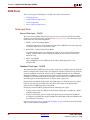
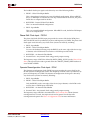
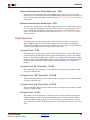
Rules for Combining I/O Standards in the Same Bank
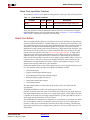
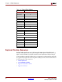
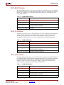
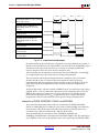
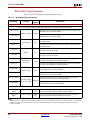
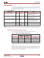
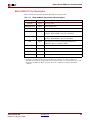
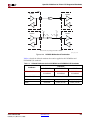
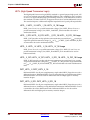
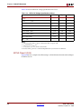
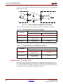
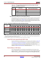
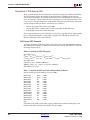
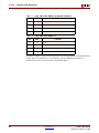
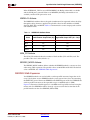
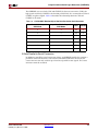
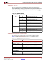
the value of VCCO. Table 6-38 describes the worst-case undershoot and overshoot at
different VCCO levels.
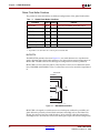
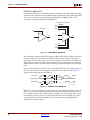
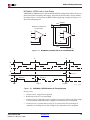
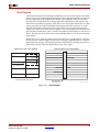
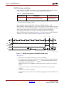
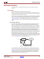
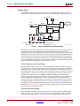
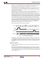
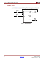
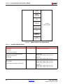
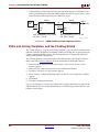
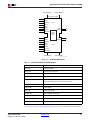
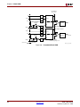
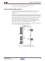
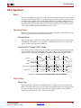
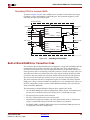
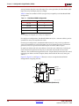
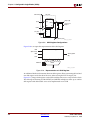
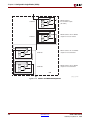
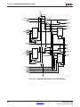
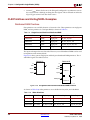
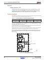
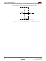
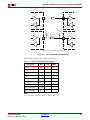
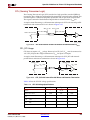
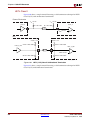
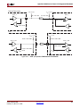
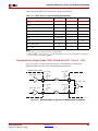
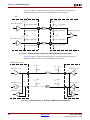
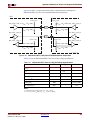
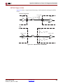
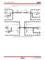
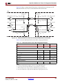
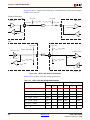
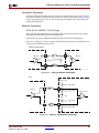
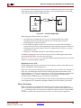
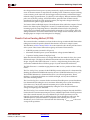
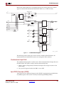
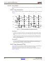
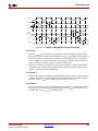
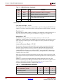
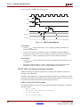
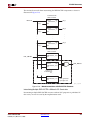
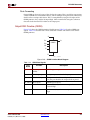
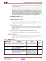
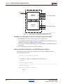
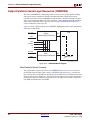
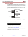
The voltage across the gate oxide at any time must not exceed 4.05V. Consider the case in
which the I/O is either an input or a 3-stated buffer as shown in Figure 6-78. The gate of the
output PMOS transistor P0 and NMOS transistor N0 is connected essentially to VCCO and
ground, respectively.
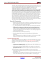
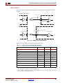
The amount of undershoot allowed without overstressing the PMOS transistor P0 is the
gate voltage minus the gate oxide limit, or VCCO – 4.05V.
Similarly, the absolute maximum overshoot allowed without overstressing the NMOS
transistor N0 is the gate voltage plus the gate oxide limit, or Ground + 4.05V.
Output Driver
Input Buffer
VCCO
VCCO
Po
Power
Clamp
Diode
External
Pin
Pi
DP
No
Ni
Ground
Clamp
Diode
DG
GND
GND
ug070_6_76_072704
Figure 6-78:
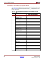
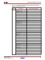
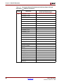
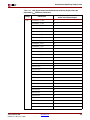
Table 6-39:
Virtex-4 I/O: 3-State Output Driver
Absolute Maximum Undershoot and Overshoot
VCCO (V)
Maximum Undershoot (V)
Maximum Overshoot (V)
3.75
–0.30
4.05
3.6
–0.45
4.05
3.45
–0.60
4.05
3.3
–0.75
4.05
3.0
–1.05
4.05
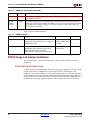
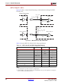
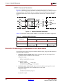
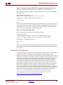
The clamp diodes offer protection against transient voltage beyond approximately
VCCO + 0.5V and Ground – 0.5V. The voltage across the diode increases proportionally to
the current going through it. Therefore the clamped level is not fixed and can vary
depending on the board design. The absolute maximum I/O limits might be exceeded
even if the clamp diode is active.
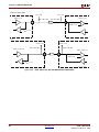
The IBIS models contain the voltage-current characteristics of the I/O drivers and clamp
diodes.
Virtex-4 User Guide
UG070 (v1.5) March 21, 2006
www.xilinx.com
291