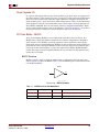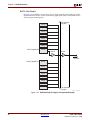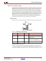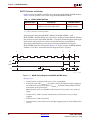
1
R
Chapter 5: Configurable Logic Blocks (CLBs)
General Slice Timing Model and Parameters
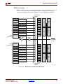
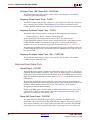
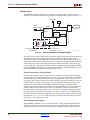
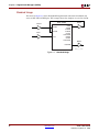
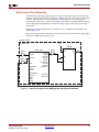
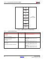
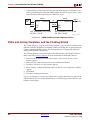
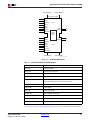
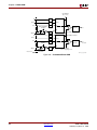
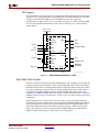
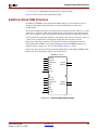
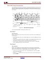
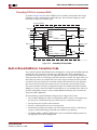
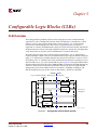
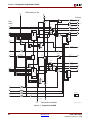
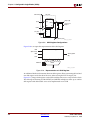
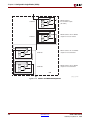
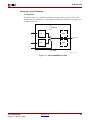
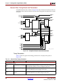
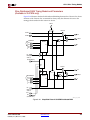
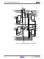
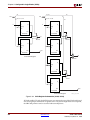
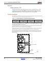
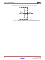
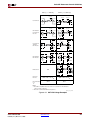
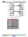
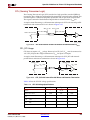
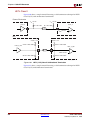
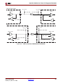
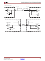
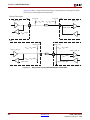
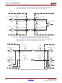
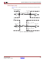
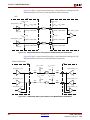
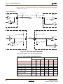
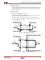
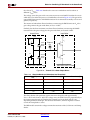
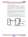
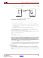
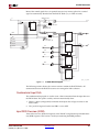
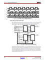
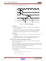
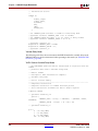
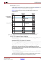
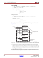
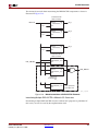
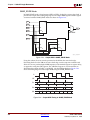
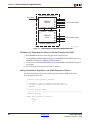
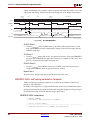
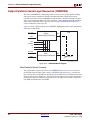
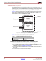
A simplified Virtex-4 slice is shown in Figure 5-20. Some elements of the Virtex-4 slice are
omitted for clarity. Only the elements relevant to the timing paths described in this section
are shown.
FXINA
FX
MUXFX
FXINB
Y
D
LUT
G
inputs
Q
YQ
FF/LAT
CE
D
CLK
SR REV
BY
F5
MUXF5
X
LUT
D
D
F
inputs
Q
XQ
FF/LAT
CE
CLK
SR REV
BX
CE
CLK
SR
UG070_5_20_071504
Figure 5-20:
Simplified Virtex-4 General SliceL/SliceM
Timing Parameters
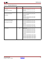
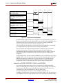
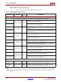
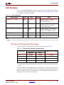
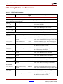
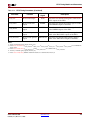
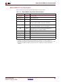
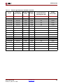
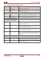
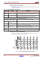
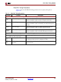
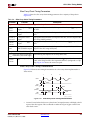
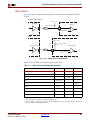
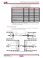
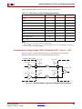
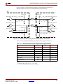
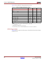
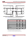
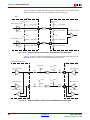
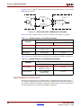
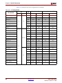
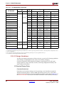
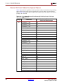
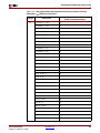
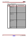
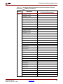
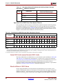
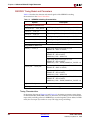
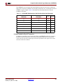
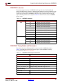
Table 5-5 shows the general slice timing parameters for a majority of the paths in
Figure 5-20.
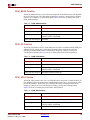
Table 5-5:
General Slice Timing Parameters
Parameter
Function
Description
Combinatorial Delays
TILO
F/G inputs to X/Y outputs
Propagation delay from the F/G inputs of the slice, through the
look-up tables (LUTs), to the X/Y outputs of the slice.
TIF5
F/G inputs to F5 output
Propagation delay from the F/G inputs of the slice, through the
LUTs and MUXF5 to the F5 output of the slice.
TIF5X
F/G inputs to XMUX
output
Propagation delay from the F/G inputs of the slice, through the
LUTs and MUXF5 to the XMUX output of the slice.
186
www.xilinx.com
Virtex-4 User Guide
UG070 (v1.5) March 21, 2006