1
CPRI MegaCore Function User Guide
CPRI MegaCore Function
User Guide
101 Innovation Drive
San Jose, CA 95134
www.altera.com
UG-01062-6.1
Document last updated for Altera Complete Design Suite version:
Document publication date:
12.1 SP1
March 2013
Feedback Subscribe
© 2013 Altera Corporation. All rights reserved. ALTERA, ARRIA, CYCLONE, HARDCOPY, MAX, MEGACORE, NIOS, QUARTUS and STRATIX words and logos
are trademarks of Altera Corporation and registered in the U.S. Patent and Trademark Office and in other countries. All other words and logos identified as
trademarks or service marks are the property of their respective holders as described at www.altera.com/common/legal.html. Altera warrants performance of its
semiconductor products to current specifications in accordance with Altera's standard warranty, but reserves the right to make changes to any products and
services at any time without notice. Altera assumes no responsibility or liability arising out of the application or use of any information, product, or service
described herein except as expressly agreed to in writing by Altera. Altera customers are advised to obtain the latest version of device specifications before relying
on any published information and before placing orders for products or services.
March 2013
Altera Corporation
ISO
9001:2008
Registered
CPRI MegaCore Function
User Guide
Contents
Chapter 1. About This MegaCore Function
General Description . . . . . . . . . . . . . . . . . . . . . . . . . . . . . . . . . . . . . . . . . . . . . . . . . . . . . . . . . . . . . . . . . . . . . 1–2
CPRI IP Core Features . . . . . . . . . . . . . . . . . . . . . . . . . . . . . . . . . . . . . . . . . . . . . . . . . . . . . . . . . . . . . . . . . . . 1–3
Device Family Support . . . . . . . . . . . . . . . . . . . . . . . . . . . . . . . . . . . . . . . . . . . . . . . . . . . . . . . . . . . . . . . . . . . 1–5
MegaCore Verification . . . . . . . . . . . . . . . . . . . . . . . . . . . . . . . . . . . . . . . . . . . . . . . . . . . . . . . . . . . . . . . . . . . 1–6
Performance and Resource Utilization . . . . . . . . . . . . . . . . . . . . . . . . . . . . . . . . . . . . . . . . . . . . . . . . . . . . . . 1–6
Release Information . . . . . . . . . . . . . . . . . . . . . . . . . . . . . . . . . . . . . . . . . . . . . . . . . . . . . . . . . . . . . . . . . . . . . 1–9
Installation and Licensing . . . . . . . . . . . . . . . . . . . . . . . . . . . . . . . . . . . . . . . . . . . . . . . . . . . . . . . . . . . . . . . . 1–9
OpenCore Plus Evaluation . . . . . . . . . . . . . . . . . . . . . . . . . . . . . . . . . . . . . . . . . . . . . . . . . . . . . . . . . . . . 1–10
OpenCore Plus Time-Out Behavior . . . . . . . . . . . . . . . . . . . . . . . . . . . . . . . . . . . . . . . . . . . . . . . . . . . . . 1–11
Chapter 2. Getting Started
MegaWizard Plug-In Manager Design Flow . . . . . . . . . . . . . . . . . . . . . . . . . . . . . . . . . . . . . . . . . . . . . . . . 2–1
Specifying Parameters . . . . . . . . . . . . . . . . . . . . . . . . . . . . . . . . . . . . . . . . . . . . . . . . . . . . . . . . . . . . . . . . . 2–2
Simulation Files . . . . . . . . . . . . . . . . . . . . . . . . . . . . . . . . . . . . . . . . . . . . . . . . . . . . . . . . . . . . . . . . . . . . . . . 2–3
Simulating the Design . . . . . . . . . . . . . . . . . . . . . . . . . . . . . . . . . . . . . . . . . . . . . . . . . . . . . . . . . . . . . . . . . 2–3
Integrating the CPRI IP Core in a Design . . . . . . . . . . . . . . . . . . . . . . . . . . . . . . . . . . . . . . . . . . . . . . . . . . . 2–5
Supporting the Transceivers . . . . . . . . . . . . . . . . . . . . . . . . . . . . . . . . . . . . . . . . . . . . . . . . . . . . . . . . . . . . 2–5
Specifying Constraints . . . . . . . . . . . . . . . . . . . . . . . . . . . . . . . . . . . . . . . . . . . . . . . . . . . . . . . . . . . . . . . . . 2–5
Compiling and Programming the Device . . . . . . . . . . . . . . . . . . . . . . . . . . . . . . . . . . . . . . . . . . . . . . . . . . . 2–6
Instantiating Multiple CPRI IP Cores . . . . . . . . . . . . . . . . . . . . . . . . . . . . . . . . . . . . . . . . . . . . . . . . . . . . . . . 2–6
Chapter 3. Parameter Settings
Physical Layer Parameters . . . . . . . . . . . . . . . . . . . . . . . . . . . . . . . . . . . . . . . . . . . . . . . . . . . . . . . . . . . . . . . . 3–1
Operation Mode Parameter . . . . . . . . . . . . . . . . . . . . . . . . . . . . . . . . . . . . . . . . . . . . . . . . . . . . . . . . . . . . 3–1
Line Rate Parameter . . . . . . . . . . . . . . . . . . . . . . . . . . . . . . . . . . . . . . . . . . . . . . . . . . . . . . . . . . . . . . . . . . . 3–2
Enable Autorate Negotiation . . . . . . . . . . . . . . . . . . . . . . . . . . . . . . . . . . . . . . . . . . . . . . . . . . . . . . . . . . . 3–2
Transceiver Starting Channel Number . . . . . . . . . . . . . . . . . . . . . . . . . . . . . . . . . . . . . . . . . . . . . . . . . . . 3–2
Rx Elastic Buffer Depth . . . . . . . . . . . . . . . . . . . . . . . . . . . . . . . . . . . . . . . . . . . . . . . . . . . . . . . . . . . . . . . . 3–3
Transceiver Reference Clock Frequency . . . . . . . . . . . . . . . . . . . . . . . . . . . . . . . . . . . . . . . . . . . . . . . . . . 3–3
Data Link Layer Parameters . . . . . . . . . . . . . . . . . . . . . . . . . . . . . . . . . . . . . . . . . . . . . . . . . . . . . . . . . . . . . . 3–4
Include MAC Block . . . . . . . . . . . . . . . . . . . . . . . . . . . . . . . . . . . . . . . . . . . . . . . . . . . . . . . . . . . . . . . . . . . 3–4
Include HDLC Block . . . . . . . . . . . . . . . . . . . . . . . . . . . . . . . . . . . . . . . . . . . . . . . . . . . . . . . . . . . . . . . . . . 3–4
Application Layer Parameters . . . . . . . . . . . . . . . . . . . . . . . . . . . . . . . . . . . . . . . . . . . . . . . . . . . . . . . . . . . . . 3–4
Mapping Mode . . . . . . . . . . . . . . . . . . . . . . . . . . . . . . . . . . . . . . . . . . . . . . . . . . . . . . . . . . . . . . . . . . . . . . . 3–5
Number of Antenna-Carrier Interfaces . . . . . . . . . . . . . . . . . . . . . . . . . . . . . . . . . . . . . . . . . . . . . . . . . . . 3–6
Enable Internally-Clocked Synchronization Mode . . . . . . . . . . . . . . . . . . . . . . . . . . . . . . . . . . . . . . . . . 3–6
Chapter 4. Functional Description
Architecture Overview . . . . . . . . . . . . . . . . . . . . . . . . . . . . . . . . . . . . . . . . . . . . . . . . . . . . . . . . . . . . . . . . . . . 4–2
Clocking Structure . . . . . . . . . . . . . . . . . . . . . . . . . . . . . . . . . . . . . . . . . . . . . . . . . . . . . . . . . . . . . . . . . . . . . . . 4–3
CPRI IP Core Clocks . . . . . . . . . . . . . . . . . . . . . . . . . . . . . . . . . . . . . . . . . . . . . . . . . . . . . . . . . . . . . . . . . . . 4–3
Clock Diagrams for the CPRI IP Core . . . . . . . . . . . . . . . . . . . . . . . . . . . . . . . . . . . . . . . . . . . . . . . . . . . . 4–5
Clock Diagrams for Most CPRI IP Core Variations . . . . . . . . . . . . . . . . . . . . . . . . . . . . . . . . . . . . . . 4–6
Clock Diagrams for CPRI IP Core Arria V GT Variations at 9830.4 Mbps . . . . . . . . . . . . . . . . . . . 4–7
Dynamically Switching Clock Mode . . . . . . . . . . . . . . . . . . . . . . . . . . . . . . . . . . . . . . . . . . . . . . . . . . . . . 4–9
CPRI Communication Link Line Rates . . . . . . . . . . . . . . . . . . . . . . . . . . . . . . . . . . . . . . . . . . . . . . . . . . 4–10
Reset Requirements . . . . . . . . . . . . . . . . . . . . . . . . . . . . . . . . . . . . . . . . . . . . . . . . . . . . . . . . . . . . . . . . . . . . . 4–11
March 2013
Altera Corporation
CPRI MegaCore Function
User Guide
iv
ContentsContents
MAP Interface . . . . . . . . . . . . . . . . . . . . . . . . . . . . . . . . . . . . . . . . . . . . . . . . . . . . . . . . . . . . . . . . . . . . . . . . . 4–12
MAP Interface Mapping Modes . . . . . . . . . . . . . . . . . . . . . . . . . . . . . . . . . . . . . . . . . . . . . . . . . . . . . . . . 4–13
Basic AxC Mapping Mode . . . . . . . . . . . . . . . . . . . . . . . . . . . . . . . . . . . . . . . . . . . . . . . . . . . . . . . . . . 4–14
Advanced AxC Mapping Modes . . . . . . . . . . . . . . . . . . . . . . . . . . . . . . . . . . . . . . . . . . . . . . . . . . . . . 4–18
MAP Receiver Interface . . . . . . . . . . . . . . . . . . . . . . . . . . . . . . . . . . . . . . . . . . . . . . . . . . . . . . . . . . . . . . . 4–18
MAP Receiver Interface Signals in Different Synchronization Modes . . . . . . . . . . . . . . . . . . . . . 4–19
MAP Receiver in FIFO Mode . . . . . . . . . . . . . . . . . . . . . . . . . . . . . . . . . . . . . . . . . . . . . . . . . . . . . . . . 4–20
MAP Receiver in Synchronous Buffer Mode . . . . . . . . . . . . . . . . . . . . . . . . . . . . . . . . . . . . . . . . . . . 4–21
MAP Receiver in the Internally-Clocked Mode . . . . . . . . . . . . . . . . . . . . . . . . . . . . . . . . . . . . . . . . 4–23
MAP Transmitter Interface . . . . . . . . . . . . . . . . . . . . . . . . . . . . . . . . . . . . . . . . . . . . . . . . . . . . . . . . . . . . 4–24
MAP Transmitter Interface Signals in Different Synchronization Modes . . . . . . . . . . . . . . . . . . 4–25
MAP Transmitter in FIFO Mode . . . . . . . . . . . . . . . . . . . . . . . . . . . . . . . . . . . . . . . . . . . . . . . . . . . . . 4–26
MAP Transmitter in Synchronous Buffer Mode . . . . . . . . . . . . . . . . . . . . . . . . . . . . . . . . . . . . . . . . 4–27
MAP Transmitter in the Internally-clocked Mode . . . . . . . . . . . . . . . . . . . . . . . . . . . . . . . . . . . . . . 4–29
Auxiliary Interface . . . . . . . . . . . . . . . . . . . . . . . . . . . . . . . . . . . . . . . . . . . . . . . . . . . . . . . . . . . . . . . . . . . . . 4–30
AUX Receiver Module . . . . . . . . . . . . . . . . . . . . . . . . . . . . . . . . . . . . . . . . . . . . . . . . . . . . . . . . . . . . . . . . 4–31
AUX Transmitter Module . . . . . . . . . . . . . . . . . . . . . . . . . . . . . . . . . . . . . . . . . . . . . . . . . . . . . . . . . . . . . 4–34
Media Independent Interface to an External Ethernet Block . . . . . . . . . . . . . . . . . . . . . . . . . . . . . . . . . . 4–37
MII Transmitter . . . . . . . . . . . . . . . . . . . . . . . . . . . . . . . . . . . . . . . . . . . . . . . . . . . . . . . . . . . . . . . . . . . . . . 4–38
MII Receiver . . . . . . . . . . . . . . . . . . . . . . . . . . . . . . . . . . . . . . . . . . . . . . . . . . . . . . . . . . . . . . . . . . . . . . . . 4–39
CPU Interface . . . . . . . . . . . . . . . . . . . . . . . . . . . . . . . . . . . . . . . . . . . . . . . . . . . . . . . . . . . . . . . . . . . . . . . . . . 4–41
Accessing the Hyperframe Control Words . . . . . . . . . . . . . . . . . . . . . . . . . . . . . . . . . . . . . . . . . . . . . . . 4–42
Recording and Retrieving the Incoming Control Words . . . . . . . . . . . . . . . . . . . . . . . . . . . . . . . . . 4–43
Writing the Outgoing Control Words . . . . . . . . . . . . . . . . . . . . . . . . . . . . . . . . . . . . . . . . . . . . . . . . 4–44
Control Word Order . . . . . . . . . . . . . . . . . . . . . . . . . . . . . . . . . . . . . . . . . . . . . . . . . . . . . . . . . . . . . . . 4–46
Control Word Transmission Example . . . . . . . . . . . . . . . . . . . . . . . . . . . . . . . . . . . . . . . . . . . . . . . . 4–46
Control Word Retrieval Example . . . . . . . . . . . . . . . . . . . . . . . . . . . . . . . . . . . . . . . . . . . . . . . . . . . . 4–47
Accessing the Ethernet Channel . . . . . . . . . . . . . . . . . . . . . . . . . . . . . . . . . . . . . . . . . . . . . . . . . . . . . . . . 4–47
Transmitting Ethernet Traffic . . . . . . . . . . . . . . . . . . . . . . . . . . . . . . . . . . . . . . . . . . . . . . . . . . . . . . . 4–48
Receiving Ethernet Traffic . . . . . . . . . . . . . . . . . . . . . . . . . . . . . . . . . . . . . . . . . . . . . . . . . . . . . . . . . . 4–49
Accessing the HDLC Channel . . . . . . . . . . . . . . . . . . . . . . . . . . . . . . . . . . . . . . . . . . . . . . . . . . . . . . . . . 4–50
CPRI Protocol Interface Layer (Physical Layer) . . . . . . . . . . . . . . . . . . . . . . . . . . . . . . . . . . . . . . . . . . . . . 4–51
Features . . . . . . . . . . . . . . . . . . . . . . . . . . . . . . . . . . . . . . . . . . . . . . . . . . . . . . . . . . . . . . . . . . . . . . . . . . . . 4–52
Physical Layer Architecture . . . . . . . . . . . . . . . . . . . . . . . . . . . . . . . . . . . . . . . . . . . . . . . . . . . . . . . . . . . 4–52
Ensuring the Physical Layer Routes Your Data as Expected . . . . . . . . . . . . . . . . . . . . . . . . . . . . . . . . 4–53
Receiver . . . . . . . . . . . . . . . . . . . . . . . . . . . . . . . . . . . . . . . . . . . . . . . . . . . . . . . . . . . . . . . . . . . . . . . . . . . . 4–53
High-Speed Transceiver . . . . . . . . . . . . . . . . . . . . . . . . . . . . . . . . . . . . . . . . . . . . . . . . . . . . . . . . . . . . 4–54
Rx Elastic Buffer . . . . . . . . . . . . . . . . . . . . . . . . . . . . . . . . . . . . . . . . . . . . . . . . . . . . . . . . . . . . . . . . . . . 4–54
Descrambling . . . . . . . . . . . . . . . . . . . . . . . . . . . . . . . . . . . . . . . . . . . . . . . . . . . . . . . . . . . . . . . . . . . . . 4–55
Frame Synchronization . . . . . . . . . . . . . . . . . . . . . . . . . . . . . . . . . . . . . . . . . . . . . . . . . . . . . . . . . . . . . 4–55
Alarm Indications . . . . . . . . . . . . . . . . . . . . . . . . . . . . . . . . . . . . . . . . . . . . . . . . . . . . . . . . . . . . . . . . . 4–56
Reset Control Word . . . . . . . . . . . . . . . . . . . . . . . . . . . . . . . . . . . . . . . . . . . . . . . . . . . . . . . . . . . . . . . . 4–57
Transmitter . . . . . . . . . . . . . . . . . . . . . . . . . . . . . . . . . . . . . . . . . . . . . . . . . . . . . . . . . . . . . . . . . . . . . . . . . 4–58
Scrambling . . . . . . . . . . . . . . . . . . . . . . . . . . . . . . . . . . . . . . . . . . . . . . . . . . . . . . . . . . . . . . . . . . . . . . . 4–59
Tx Elastic Buffer . . . . . . . . . . . . . . . . . . . . . . . . . . . . . . . . . . . . . . . . . . . . . . . . . . . . . . . . . . . . . . . . . . . 4–59
High-Speed Transceiver . . . . . . . . . . . . . . . . . . . . . . . . . . . . . . . . . . . . . . . . . . . . . . . . . . . . . . . . . . . . 4–59
Chapter 5. Testing Features
Loopback Modes . . . . . . . . . . . . . . . . . . . . . . . . . . . . . . . . . . . . . . . . . . . . . . . . . . . . . . . . . . . . . . . . . . . . . . . . 5–1
External Loopback . . . . . . . . . . . . . . . . . . . . . . . . . . . . . . . . . . . . . . . . . . . . . . . . . . . . . . . . . . . . . . . . . . . . 5–1
Internal Reverse Loopback . . . . . . . . . . . . . . . . . . . . . . . . . . . . . . . . . . . . . . . . . . . . . . . . . . . . . . . . . . . . . 5–2
Physical Layer Loopback Mode . . . . . . . . . . . . . . . . . . . . . . . . . . . . . . . . . . . . . . . . . . . . . . . . . . . . . . . 5–2
Reverse Loopback Through CPRI Rx and Tx Buffers . . . . . . . . . . . . . . . . . . . . . . . . . . . . . . . . . . . . 5–2
PRBS Generation and Validation . . . . . . . . . . . . . . . . . . . . . . . . . . . . . . . . . . . . . . . . . . . . . . . . . . . . . . . . . . 5–2
CPRI MegaCore Function
User Guide
March 2013 Altera Corporation
ContentsContents
v
Achieving Link Synchronization Without an REC Master . . . . . . . . . . . . . . . . . . . . . . . . . . . . . . . . . . . . . 5–4
Chapter 6. Signals
MAP Interface Signals . . . . . . . . . . . . . . . . . . . . . . . . . . . . . . . . . . . . . . . . . . . . . . . . . . . . . . . . . . . . . . . . . . . 6–1
MAP Receiver Signals . . . . . . . . . . . . . . . . . . . . . . . . . . . . . . . . . . . . . . . . . . . . . . . . . . . . . . . . . . . . . . . . . 6–1
MAP Transmitter Signals . . . . . . . . . . . . . . . . . . . . . . . . . . . . . . . . . . . . . . . . . . . . . . . . . . . . . . . . . . . . . . 6–3
Auxiliary Interface Signals . . . . . . . . . . . . . . . . . . . . . . . . . . . . . . . . . . . . . . . . . . . . . . . . . . . . . . . . . . . . . . . . 6–5
AUX Receiver Signals . . . . . . . . . . . . . . . . . . . . . . . . . . . . . . . . . . . . . . . . . . . . . . . . . . . . . . . . . . . . . . . . . 6–6
AUX Transmitter Signals . . . . . . . . . . . . . . . . . . . . . . . . . . . . . . . . . . . . . . . . . . . . . . . . . . . . . . . . . . . . . . . 6–7
Extended Rx Status Signals . . . . . . . . . . . . . . . . . . . . . . . . . . . . . . . . . . . . . . . . . . . . . . . . . . . . . . . . . . . . . 6–9
CPRI MII Signals . . . . . . . . . . . . . . . . . . . . . . . . . . . . . . . . . . . . . . . . . . . . . . . . . . . . . . . . . . . . . . . . . . . . . . . 6–10
CPRI MII Receiver Signals . . . . . . . . . . . . . . . . . . . . . . . . . . . . . . . . . . . . . . . . . . . . . . . . . . . . . . . . . . . . 6–10
CPRI MII Transmitter Signals . . . . . . . . . . . . . . . . . . . . . . . . . . . . . . . . . . . . . . . . . . . . . . . . . . . . . . . . . . 6–10
CPU Interface Signals . . . . . . . . . . . . . . . . . . . . . . . . . . . . . . . . . . . . . . . . . . . . . . . . . . . . . . . . . . . . . . . . . . . 6–11
Physical Layer Signals . . . . . . . . . . . . . . . . . . . . . . . . . . . . . . . . . . . . . . . . . . . . . . . . . . . . . . . . . . . . . . . . . . 6–12
CPRI Data Signals . . . . . . . . . . . . . . . . . . . . . . . . . . . . . . . . . . . . . . . . . . . . . . . . . . . . . . . . . . . . . . . . . . . . 6–12
Layer 1 Clock and Reset Signals . . . . . . . . . . . . . . . . . . . . . . . . . . . . . . . . . . . . . . . . . . . . . . . . . . . . . . . . 6–13
Layer 1 Error Signal . . . . . . . . . . . . . . . . . . . . . . . . . . . . . . . . . . . . . . . . . . . . . . . . . . . . . . . . . . . . . . . . . . 6–13
Autorate Negotiation Signals . . . . . . . . . . . . . . . . . . . . . . . . . . . . . . . . . . . . . . . . . . . . . . . . . . . . . . . . . . 6–13
Transceiver Signals . . . . . . . . . . . . . . . . . . . . . . . . . . . . . . . . . . . . . . . . . . . . . . . . . . . . . . . . . . . . . . . . . . . 6–15
Clock and Reset Interface Signals . . . . . . . . . . . . . . . . . . . . . . . . . . . . . . . . . . . . . . . . . . . . . . . . . . . . . . . . . 6–17
Chapter 7. Software Interface
CPRI Protocol Interface Registers . . . . . . . . . . . . . . . . . . . . . . . . . . . . . . . . . . . . . . . . . . . . . . . . . . . . . . . . . . 7–2
MAP Interface and AUX Interface Configuration Registers . . . . . . . . . . . . . . . . . . . . . . . . . . . . . . . . . . . 7–15
Ethernet Registers . . . . . . . . . . . . . . . . . . . . . . . . . . . . . . . . . . . . . . . . . . . . . . . . . . . . . . . . . . . . . . . . . . . . . . 7–22
HDLC Registers . . . . . . . . . . . . . . . . . . . . . . . . . . . . . . . . . . . . . . . . . . . . . . . . . . . . . . . . . . . . . . . . . . . . . . . . 7–27
Chapter 8. Testbenches
Test Sequence . . . . . . . . . . . . . . . . . . . . . . . . . . . . . . . . . . . . . . . . . . . . . . . . . . . . . . . . . . . . . . . . . . . . . . . . . . . 8–6
Reset, Frame Synchronization, and Initialization . . . . . . . . . . . . . . . . . . . . . . . . . . . . . . . . . . . . . . . . . . . . . 8–7
Running the Testbenches . . . . . . . . . . . . . . . . . . . . . . . . . . . . . . . . . . . . . . . . . . . . . . . . . . . . . . . . . . . . . . . . . 8–8
Appendix A. Initialization Sequence
Appendix B. Implementing CPRI Link Autorate Negotiation
Design Implementation . . . . . . . . . . . . . . . . . . . . . . . . . . . . . . . . . . . . . . . . . . . . . . . . . . . . . . . . . . . . . . . . .
Configuring the CPRI IP Core for Autorate Negotiation . . . . . . . . . . . . . . . . . . . . . . . . . . . . . . . . . . . . .
Running Autorate Negotiation . . . . . . . . . . . . . . . . . . . . . . . . . . . . . . . . . . . . . . . . . . . . . . . . . . . . . . . . . . .
Autorate Negotiation From 9.8304 Gbps in Arria V GT Variations . . . . . . . . . . . . . . . . . . . . . . . . . . . .
B–1
B–3
B–3
B–4
Appendix C. Advanced AxC Mapping Modes
Backward Compability . . . . . . . . . . . . . . . . . . . . . . . . . . . . . . . . . . . . . . . . . . . . . . . . . . . . . . . . . . . . . . . . . .
Advanced Mapping Mode Similarities and Differences . . . . . . . . . . . . . . . . . . . . . . . . . . . . . . . . . . . . . .
Fifteen-Bit Width Mode . . . . . . . . . . . . . . . . . . . . . . . . . . . . . . . . . . . . . . . . . . . . . . . . . . . . . . . . . . . . . . .
Sixteen-Bit Width Mode . . . . . . . . . . . . . . . . . . . . . . . . . . . . . . . . . . . . . . . . . . . . . . . . . . . . . . . . . . . . . .
C–1
C–2
C–3
C–4
Appendix D. Delay Measurement and Calibration
Altera Delay Measurement and Calibration Features . . . . . . . . . . . . . . . . . . . . . . . . . . . . . . . . . . . . . . . .
Delay Requirements . . . . . . . . . . . . . . . . . . . . . . . . . . . . . . . . . . . . . . . . . . . . . . . . . . . . . . . . . . . . . . . . . . . .
Rx Path Delay . . . . . . . . . . . . . . . . . . . . . . . . . . . . . . . . . . . . . . . . . . . . . . . . . . . . . . . . . . . . . . . . . . . . . . . . . .
Rx Path Delay Components . . . . . . . . . . . . . . . . . . . . . . . . . . . . . . . . . . . . . . . . . . . . . . . . . . . . . . . . . . .
Rx Path Delay Components in Most CPRI IP Core Variations . . . . . . . . . . . . . . . . . . . . . . . . . . . .
March 2013
Altera Corporation
D–1
D–1
D–3
D–3
D–3
CPRI MegaCore Function
User Guide
vi
ContentsContents
Rx Path Delay Components in Some Specific Arria V GT Variations . . . . . . . . . . . . . . . . . . . . . . D–5
Rx Transceiver Latency . . . . . . . . . . . . . . . . . . . . . . . . . . . . . . . . . . . . . . . . . . . . . . . . . . . . . . . . . . . . . . . D–5
Extended Rx Delay Measurement . . . . . . . . . . . . . . . . . . . . . . . . . . . . . . . . . . . . . . . . . . . . . . . . . . . . . . D–7
M/N Ratio Selection . . . . . . . . . . . . . . . . . . . . . . . . . . . . . . . . . . . . . . . . . . . . . . . . . . . . . . . . . . . . . . . D–7
Arria V GT Variations Originally Configured with CPRI Line Rate 9.8 Gbps . . . . . . . . . . . . . . . D–7
CPRI Receive Buffer Delay Calculation Example . . . . . . . . . . . . . . . . . . . . . . . . . . . . . . . . . . . . . . . D–8
Round-Trip Calibration Delay in Rx Path . . . . . . . . . . . . . . . . . . . . . . . . . . . . . . . . . . . . . . . . . . . . . . . D–9
Fixed Rx Core Delay Component . . . . . . . . . . . . . . . . . . . . . . . . . . . . . . . . . . . . . . . . . . . . . . . . . . . . . . . D–9
Rx Path Delay to AUX Output: Calculation Example . . . . . . . . . . . . . . . . . . . . . . . . . . . . . . . . . . . . . D–10
Tx Path Delay . . . . . . . . . . . . . . . . . . . . . . . . . . . . . . . . . . . . . . . . . . . . . . . . . . . . . . . . . . . . . . . . . . . . . . . . . D–11
Tx Path Delay Components . . . . . . . . . . . . . . . . . . . . . . . . . . . . . . . . . . . . . . . . . . . . . . . . . . . . . . . . . . D–11
Tx Path Delay Components in Most CPRI IP Core Variations . . . . . . . . . . . . . . . . . . . . . . . . . . . D–11
Tx Path Delay Components in Some Specific Arria V GT Variations . . . . . . . . . . . . . . . . . . . . . D–12
Fixed Tx Core Delay Component . . . . . . . . . . . . . . . . . . . . . . . . . . . . . . . . . . . . . . . . . . . . . . . . . . . . . . D–13
Extended Tx Delay Measurement . . . . . . . . . . . . . . . . . . . . . . . . . . . . . . . . . . . . . . . . . . . . . . . . . . . . . D–13
Tx Bitslip Delay . . . . . . . . . . . . . . . . . . . . . . . . . . . . . . . . . . . . . . . . . . . . . . . . . . . . . . . . . . . . . . . . . . . . . D–13
Tx Transceiver Latency . . . . . . . . . . . . . . . . . . . . . . . . . . . . . . . . . . . . . . . . . . . . . . . . . . . . . . . . . . . . . . D–14
T14, Toffset, Round-Trip Delay, and Round-Trip Cable Delay Calculations . . . . . . . . . . . . . . . . . . . . D–15
Round-Trip and Cable Delay Calculations for a Single-Hop Configuration . . . . . . . . . . . . . . . . . D–16
Tx Bitslip Delay in the Round-Trip Delay Calculation . . . . . . . . . . . . . . . . . . . . . . . . . . . . . . . . . D–17
Single-Hop Round-Trip and Cable Delay Calculation Examples . . . . . . . . . . . . . . . . . . . . . . . . D–17
Dynamic Pipelining for Automatic Round-Trip Delay Calibration . . . . . . . . . . . . . . . . . . . . . . . . . D–22
Round-Trip Calculations for a Multihop Configuration . . . . . . . . . . . . . . . . . . . . . . . . . . . . . . . . . . D–23
Multihop Round-Trip Delay Calculation . . . . . . . . . . . . . . . . . . . . . . . . . . . . . . . . . . . . . . . . . . . . . D–24
Multihop Round-Trip Cable Delay Calculation . . . . . . . . . . . . . . . . . . . . . . . . . . . . . . . . . . . . . . . D–24
Two-Hop Round-Trip and Cable Delay Calculation Example . . . . . . . . . . . . . . . . . . . . . . . . . . . D–24
Appendix E. Integrating the CPRI IP Core Timing Constraints in the Full Design
Appendix F. Porting a CPRI IP Core from the Previous Version of the Software
Additional Information
Document Revision History . . . . . . . . . . . . . . . . . . . . . . . . . . . . . . . . . . . . . . . . . . . . . . . . . . . . . . . . . . . Info–1
How to Contact Altera . . . . . . . . . . . . . . . . . . . . . . . . . . . . . . . . . . . . . . . . . . . . . . . . . . . . . . . . . . . . . . . . Info–5
Typographic Conventions . . . . . . . . . . . . . . . . . . . . . . . . . . . . . . . . . . . . . . . . . . . . . . . . . . . . . . . . . . . . . Info–5
CPRI MegaCore Function
User Guide
March 2013 Altera Corporation
1. About This MegaCore Function
The Altera® CPRI MegaCore® function implements the Common Public Radio
Interface (CPRI) specification. CPRI is a high-speed serial interface designed for
network radio equipment controllers (REC) to receive data from and provide data to
remote radio equipment (RE).
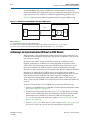
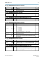
The CPRI IP core targets high-performance, remote, radio network applications. You
can configure the CPRI IP core as an RE or an REC. Figure 1–1 shows an example
system implementation with a two-hop daisy chain. Optical links between devices
support high performance.
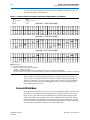
Figure 1–1. Typical CPRI Application on Altera Devices
RF
RF
Routing Layer
MAP
AUX
CPRI
MegaCore Function
(RE Slave)
AUX
CPRI
MegaCore Function
(RE Master)
CPRI
CPRI
Optical Link
CPRI
MAP
FPGA
CPRI
MegaCore Function
(RE Slave)
CPRI
FPGA
Optical Link
FPGA
CPRI
MegaCore Function
(REC)
Clock
Base Band Module Module
March 2013
Altera Corporation
CPRI MegaCore Function
User Guide
1–2
Chapter 1: About This MegaCore Function
General Description
General Description
The Altera CPRI IP core implements Layer 1 and Layer 2 of the CPRI V5.0
specification. It provides access to the V5.0 Layer 1 and Layer 2 access points through
various interfaces:
■
■
■
■
■
■
V5.0 Layer 1 access:
■
Auxiliary (AUX) interface for full access to V5.0 control data stream for
antenna-carrier (Ctrl_AxC) bytes in control word.
■
Register support for loading and unloading full control words, including
Ctrl_AxC bytes.
■
Auxiliary (AUX) interface support for user-defined GSM mapping.
IQ data access:
■
Mapping block (MAP) to antenna-carrier interfaces for easy IQ user data plane
access based on pre-configured antenna-carrier channels.
■
Auxiliary (AUX) interface for full access to the user data plane.
Ethernet channel access:
■
Auxiliary interface for full access to the Ethernet space in the CPRI frame.
■
Register support for loading and unloading the Ethernet frame.
■
Media independent (MI) interface port for Ethernet Frame access.
High level data link control (HDLC) channel access:
■
Auxiliary interface for full access to the HDLC space in the CPRI frame.
■
Register support for loading and unloading the HDLC frame.
Vendor-specific data (VSS):
■
Auxiliary interface for full access to control words.
■
Register support for loading and unloading full control words, including VSS
space.
Synchronization and timing access:
■
Auxiliary interface for full access to synchronization and timing.
You configure the CPRI IP core to include an Ethernet media access control (MAC)
block or to communicate with an external Ethernet module through an MI interface.
You can configure the CPRI link line rate.
For information about the CPRI IP core interfaces and functionality, refer to Chapter 4,
Functional Description. For information about configuration options, refer to
Chapter 3, Parameter Settings.
CPRI MegaCore Function
User Guide
March 2013 Altera Corporation
Chapter 1: About This MegaCore Function
CPRI IP Core Features
1–3
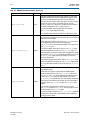
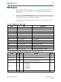
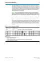
Figure 1–2 shows the CPRI IP core interfaces. The IP core assembles the outbound
CPRI frame control words and data from all of these interfaces, and unloads and
routes control words and data from the inbound CPRI frame to the appropriate
interfaces, based on configuration and register settings.
Figure 1–2. CPRI IP Core Interfaces
AUX
Interface
MAP
Interface (1)
Full access
to
CPRI frame
IQ
Data
MI
Interface
CPU
Interface
Vendor
Specific
L1
Inband
Protocol
HDLC (2)
Ethernet (3)
Time Division Multiplexing
Multiplexing
Transmitter
Transmitter
Transceiver
Receiver
Receiver
Transceiver
tx_dataout
rx_datain
CPRI Link
CPRI Link
Notes to Figure 1–2:
(1) You can configure your CPRI IP core with zero, one, or multiple antenna-carrier interfaces. If you configure zero antenna-carrier interfaces, the
MAP interface is not configured in your CPRI IP core. In that case you can communicate IQ data through the AUX interface to your user-defined
routing layer.
(2) You can configure your CPRI IP core with or without an HDLC block.
(3) You can configure your CPRI IP core with an Ethernet MAC block or a media-independent (MI) interface (MII) block. The two options are mutually
exclusive.
CPRI IP Core Features
The CPRI IP core has the following features:
March 2013
■
Complies with the Common Public Radio Interface (CPRI) Specification V5.0
(2011-09-21) Interface Specification for wireless base station submodule
interconnections, without the full range of IQ data sample widths, using auxiliary
interface for user-defined GSM mapping.
■
Supports radio equipment controller (REC) and radio equipment (RE) module
configurations, including RE master, RE slave, and REC master ports.
■
Supports Universal Mobile Telecommunication System (UMTS) Terrestrial Radio
Access (UTRA) – frequency division duplexing (UTRA-FDD) (UMTS/Wideband
Code Division Multiple Access (W-CDMA)), Evolved UTRA (E-UTRA) (3rd
Generation Partnership Project (3GPP) Long Term Evolution (LTE) specification),
3GPP Global System for Mobile Communications (GSM)/Enhanced Data Rates for
GSM Evolution (EDGE) Radio Access Network, and Worldwide interoperability
for Microwave Access (WiMAX) (IEEE 802.16 standard).
■
Provides full access to CPRI frame.
Altera Corporation
CPRI MegaCore Function
User Guide
1–4
Chapter 1: About This MegaCore Function
CPRI IP Core Features
■
■
Supports the following additional CPRI link features:
■
Programmable CPRI communication line rate (to 614.4, 1228.8, 2457.6, 3072.0,
4915.2, 6144.0, or 9830.4 Mbps) using Altera on-chip high-speed transceivers.
■
Programmable operation mode: CPRI link master or CPRI link slave.
■
Auto-rate negotiation support.
■
Scrambling and descrambling at 4915.2 Mbps, 6144.0 Mbps, and 9830.4 Mbps.
■
Receiver (Rx) delay measurement.
■
Transmitter (Tx) delay calibration.
■
Programmable hardware processing of the reset request bit in the CPRI frame.
■
Vendor-specific subchannel (VSS) communication on the CPRI link.
■
Diagnostic parallel reverse loopback paths.
■
Diagnostic stand-alone RE slave testing mode.
Includes the following additional interfaces:
■
Interface to external or on-chip processor, using the Altera Avalon®
Memory-Mapped (Avalon-MM) interconnect specification.
■
Ethernet communication interfaces that support simultaneous Ethernet and
HDLC communication to and from the CPRI link.
■
■
CPRI MegaCore Function
User Guide
■
Optional configuration of Ethernet MAC.
■
Optional Media-Independent Interface for Ethernet frame access.
■
Optional configuration of HDLC block.
Auxiliary interface provides full access to CPRI frame.
■
Supports data transfer to and from custom mapping functions, including
user-defined GSM mapping.
■
Supports data transfer from slave to master ports to implement daisy-chain
topologies.
■
Supports custom IQ sample widths.
Optional built-in IQ data interface with the following features:
■
Implements mapping methods in Sections 4.2.7.2.5 and 4.2.7.2.7 of the CPRI
V4.2 Specification, and mapping Options 1 and 2 in Sections 4.2.7.2.3 and
4.2.7.2.4 of the CPRI V4.2 Specification.
■
Implements WiMAX mapping methods described in Sections 4.2.7.2.2,
4.2.7.2.5, and 4.2.7.2.7 of the CPRI V4.2 Specification.
■
Implements UMTS/LTE mapping methods described in Section 4.2.7.2 of
the CPRI V4.2 Specification.
■
Implements WiMAX timing control methodology described in Section
4.2.8.2 of the CPRI V4.2 Specification.
■
Supports as many as 24 antenna-carrier interfaces.
■
Supports clocking antenna-carrier interfaces with external data channel
clocks or internal IP core clock.
March 2013 Altera Corporation
Chapter 1: About This MegaCore Function
Device Family Support
1–5
■
Supports synchronous buffer or simple FIFO synchronization modes for
externally clocked antenna-carrier interfaces.
■
Supports independent sample rates for each antenna-carrier interface.
■
Supports 15- and 16-bit data sample widths on uplink and downlink using
the Altera Avalon Streaming (Avalon-ST) interconnect specification.
Device Family Support
Table 1–1 defines the device support levels for Altera IP cores.
Table 1–1. Altera IP Core Device Support Levels
FPGA Device Families
HardCopy Device Families
Preliminary support—The IP core is verified with
preliminary timing models for this device family. The IP core
meets all functional requirements, but might still be
undergoing timing analysis for the device family. It can be
used in production designs with caution.
HardCopy Companion—The IP core is verified with
preliminary timing models for the HardCopy companion
device. The IP core meets all functional requirements, but
might still be undergoing timing analysis for the HardCopy
device family. It can be used in production designs with
caution.
Final support—The IP core is verified with final timing
models for this device family. The IP core meets all
functional and timing requirements for the device family and
can be used in production designs.
HardCopy Compilation—The IP core is verified with final
timing models for the HardCopy device family. The IP core
meets all functional and timing requirements for the device
family and can be used in production designs.
Table 1–2 lists the level of support offered by the CPRI IP core for each Altera device
family.
Table 1–2. Device Family Support
Device Family
Support
Refer to the What’s New in Altera IP page of
the Altera website.
Stratix® V
Stratix IV GX
Final
HardCopy® IV GX
HardCopy Compilation
Arria® V (GX, GT, and GZ (1) variants)
Preliminary
Arria II (GX and GZ variants)
Final
Cyclone®
Preliminary
V
GX (2)
Cyclone IV GX
Final
Other device families
No support
Notes to Table 1–2:
(1) Arria V GZ support to CPRI line rates up to 6.144 Gbps is available starting with the Quartus II v12.1 software
release. Arria V GZ support to CPRI line rate of 9.8304 Gbps is available starting with the Quartus II v12.1 SP1
software release.
(2) Cyclone V GX support is available starting with the Quartus II v12.1 software release.
March 2013
Altera Corporation
CPRI MegaCore Function
User Guide
1–6
Chapter 1: About This MegaCore Function
MegaCore Verification
MegaCore Verification
Before releasing a version of the CPRI IP core, Altera runs comprehensive regression
tests in the current version of the Quartus® II software. These tests use the
MegaWizard™ Plug-In Manager to create the instance files. Altera tests these files in
simulation and hardware to confirm functionality.
Altera tests and verifies the CPRI IP core in hardware, especially the deterministic
latency feature, for different platforms and environments.
Performance and Resource Utilization
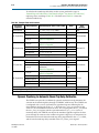
This section contains tables showing IP core variation size and performance examples.
For resource utilization information for additional CPRI IP core variations, refer to the
reports the Quartus II software generates during compilation.
Table 1–3 lists the resources and expected performance for CPRI IP core variations
configured with the following features:
■
Operate in REC master mode
■
Include autorate negotiation support
■
Provide Ethernet access through the MI interface
■
Do not provide an HDLC block
■
Use Basic mapping mode
■
Clock the AxC channels with independent clocks (the Enable MAP interface
synchronization with core clock parameter is turned off)
The numbers of ALMs and logic registers are rounded up to the nearest 100.
Table 1–3 lists results obtained with the Quartus II software v12.1 SP1 for the
following devices:
CPRI MegaCore Function
User Guide
■
Stratix V GX (5SGXMA5N3F40I4
■
Arria V GT (5AGTMD3G3F31I3)
■
Arria V GX (5AGXFB3H6F35C6 for 614.4, 1228.8, 2457.6, and 3072 Mbps variations
and 5AGXFB3H4F35I5 for other variations)
■
Arria V GZ (5AGZME7K3F40I4)
March 2013 Altera Corporation
Chapter 1: About This MegaCore Function
Performance and Resource Utilization
■
1–7
Cyclone V GX (5CGXFC9E7F35C8 for 6144 Mbps variations and 5CGXFC9E6F35I7
for 122.8, 2457.6, and 3072 Mbps variations)
Table 1–3. CPRI IP Core FPGA Resource Utilization (Part 1 of 2)
Parameters
Device
Line Rate
(Mbps)
614.4
Stratix V GX
1228.8,
2457.6,
3072,
4915.2
6144,
9830.4
Arria V GT
6144,
9830.4
614.4
Arria V GX
1228.8,
2457.6,
3072
4915.2,
6144
March 2013
Altera Corporation
Memory
Number of
Antenna-Carrier
Interfaces
ALMs
Logic Registers
M10K or M20K
Blocks (1)
0
2700
3100
10
1
3300
4100
16
2
3500
4300
18
3
3700
4600
20
4
3900
4900
22
0
2500
3100
10
1
3100
4000
16
4
3600
4800
22
8
4300
5800
30
0
4000
6200
10
1
4200
8100
16
4
5600
8900
22
8
6300
10100
30
0
3300
5500
16
1
4800
7400
28
4
4600
8100
34
8
5900
9100
42
0
2600
3100
12
1
3300
4000
22
2
3400
4200
24
3
3600
4400
26
4
3800
4700
28
0
2400
3000
12
1
3000
3900
22
4
3400
4600
28
8
4000
5400
36
0
3700
5600
16
1
4700
7300
28
4
5200
8200
34
8
5800
9100
42
CPRI MegaCore Function
User Guide
1–8
Chapter 1: About This MegaCore Function
Performance and Resource Utilization
Table 1–3. CPRI IP Core FPGA Resource Utilization (Part 2 of 2)
Parameters
Device
Line Rate
(Mbps)
Number of
Antenna-Carrier
Interfaces
ALMs
Logic Registers
M10K or M20K
Blocks (1)
0
2600
3100
10
1
3500
4200
16
2
3700
4500
18
3
3800
4800
20
4
4100
5000
22
0
2400
3100
10
1
3300
4200
16
4
3800
5000
22
8
4300
6000
30
0
4000
6200
10
1
5200
8200
16
4
5700
9100
22
8
6500
10300
30
0
2600
2800
12
1
3500
3700
22
2
3600
3900
24
3
3800
4200
26
4
4000
4400
28
0
2400
2800
12
1
3200
3700
22
4
3700
4400
28
8
4300
5300
36
614.4
Arria V GZ
Memory
1228.8,
2457.6,
3072,
4915.2
6144,
9830.4
614.4
Cyclone V GX
1228.8,
2457.6,
3072
Note to Table 1–3:
(1) M10K blocks in Arria V GX, Arria V GT, and Cyclone V GX devices and M20K blocks in Arria V GZ and Stratix V devices.
Table 1–4 shows the slowest device family speed grade that supports each CPRI line
rate in each device family. Lower speed grade numbers correspond to faster devices.
Table 1–4. Slowest Recommended Device Family Speed Grades (1) (Part 1 of 2)
Device Family
or Variant
CPRI Line Rate (Mbps)
614.4
1228.8
2457.6
3072.0
4915.2
6144
9830.4
Stratix V GX
–4
–4
–4
–4
–4
–4
-2
Stratix IV GX
–4
–4
–4
–4
–4
–3
(3)
Arria V GT
C6
C6
C6
I5
I5
I5
I5
Arria V GX
C6
C6
C6
I5
I5
I5
(3)
Arria V GZ
–4
–4
–4
–4
–4
–4
–3
–6
I3 (2)
I3 (2)
(3)
Arria II GX
CPRI MegaCore Function
User Guide
–6
–6
–6
March 2013 Altera Corporation
Chapter 1: About This MegaCore Function
Release Information
1–9
Table 1–4. Slowest Recommended Device Family Speed Grades (1) (Part 2 of 2)
Device Family
or Variant
CPRI Line Rate (Mbps)
614.4
1228.8
2457.6
3072.0
4915.2
6144
9830.4
Arria II GZ
–4
–4
–4
–4
–3
–3
(3)
Cyclone V GX
C8
–7
–7
–7
(3)
(3)
(3)
Cyclone IV GX
C8, I7
C8, I7
C8, I7
–7
(3)
(3)
(3)
Notes to Table 1–4:
(1) The entry –x indicates that both the industrial speed grade Ix and the commercial speed grade Cx are supported for this device family and CPRI
line rate.
(2) Only the I3 speed grade is available for a CPRI IP core that runs at this line rate and targets the Arria II GX device family.
(3) This CPRI line rate is not supported for this device family.
Release Information
Table 1–5 provides information about this release of the CPRI IP core.
Table 1–5. CPRI Release Information
Item
Version
Release Date
Ordering Code
Description
12.1 SP1
February 2013
IP-CPRI
Product ID
00CB
Vendor ID
6AF7
Altera verifies that the current version of the Quartus II software compiles the
previous version of each Altera IP core. Any exceptions to this verification are
reported in the MegaCore IP Library Release Notes and Errata. Altera does not verify
compilation with IP core versions older than the previous release.
Installation and Licensing
The CPRI IP core is part of the MegaCore IP Library, which is distributed with the
Quartus II software. The combined software is downloadable from the Altera website,
www.altera.com.
March 2013
Altera Corporation
CPRI MegaCore Function
User Guide
1–10
Chapter 1: About This MegaCore Function
Installation and Licensing
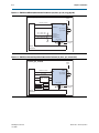
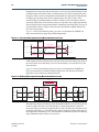
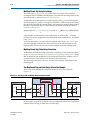
Figure 1–3 shows the directory structure after you install the CPRI IP core, where
<path> is the installation directory. The default installation directory on Windows is
C:\altera\<version number>; on Linux it is /opt/altera<version number>.
Figure 1–3. Directory Structure
<path>
Installation directory
ip
Contains the Altera MegaCore IP Library and third-party IP cores
altera
Contains the Altera MegaCore IP Library
common
Contains shared components
cpri
Contains the CPRI IP core files
src
Contains the CPRI IP core encrypted lower-level design files
constraints
Contains the Synopsys Design Constraints and Tcl constraints scripts for the CPRI IP core
cus_demo_tb
Contains the demonstration testbenches for the CPRI IP core
You can use Altera’s free OpenCore Plus evaluation feature to evaluate the CPRI IP
core in simulation and in hardware before you purchase a license. You must purchase
a license for the CPRI IP core only when you are satisfied with its functionality and
performance, and you want to take your design to production.
After you purchase a license for the CPRI IP core, you can request a license file from
the Altera website at www.altera.com/licensing and install it on your computer.
When you request a license file, Altera emails you a license.dat file. If you do not have
internet access, contact your local Altera representative.
OpenCore Plus Evaluation
With the Altera free OpenCore Plus evaluation feature, you can perform the following
actions:
CPRI MegaCore Function
User Guide
■
Simulate the behavior of a megafunction (Altera IP core or AMPPSM
megafunction) in your system using the Quartus II software and Altera-supported
VHDL and Verilog HDL simulators
■
Verify the functionality of your design and evaluate its size and speed quickly and
easily
■
Generate time-limited device programming files for designs that include Altera IP
cores
■
Program a device and verify your design in hardware
March 2013 Altera Corporation
Chapter 1: About This MegaCore Function
Installation and Licensing
1–11
OpenCore Plus Time-Out Behavior
OpenCore Plus hardware evaluation supports the following two operation modes:
■
Untethered—the design runs for a limited time.
■
Tethered—requires a connection between your board and the host computer. If
tethered mode is supported by all megafunctions in a design, the device can
operate for a longer time or indefinitely.
All megafunctions in a device time out simultaneously when the most restrictive
evaluation time is reached. If there is more than one megafunction in a design, a
specific megafunction's time-out behavior might be masked by the time-out behavior
of the other megafunctions.
1
For Altera IP cores, the untethered time-out is 1 hour; the tethered time-out value is
indefinite.
Your design stops working after the hardware evaluation time expires.
The CPRI IP core then behaves as if the reset and cpu_reset signals are asserted: the
CPRI link and the CPU interface reset. The transceivers do not reset, because the
transceiver quad might be shared with other designs, IP cores, and megafunctions.
The CPRI IP core cannot achieve frame synchronization, and cannot participate in
further CPRI communication.
f For information about installation and licensing, refer to Altera Software Installation and
Licensing. For information about the OpenCore Plus evaluation feature, refer to
AN 320: OpenCore Plus Evaluation of Megafunctions.
March 2013
Altera Corporation
CPRI MegaCore Function
User Guide
1–12
CPRI MegaCore Function
User Guide
Chapter 1: About This MegaCore Function
Installation and Licensing
March 2013 Altera Corporation
2. Getting Started
You can customize the CPRI IP core to support a wide variety of applications. You use
the MegaWizard Plug-In Manager in the Quartus II software to parameterize a
custom IP core variation in a CPRI parameter editor. The CPRI parameter editor lets
you interactively set parameter values and select optional ports.
The CPRI IP core supports the Altera MegaWizard Plug-In Manager design flow. The
CPRI IP core is not available in the Qsys design flow. To include a CPRI IP core in your
Qsys-based design, you must generate the IP core in the MegaWizard Plug-In
Manager design flow and connect it manually in the design.
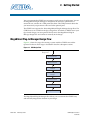
MegaWizard Plug-In Manager Design Flow
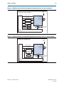
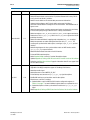
Figure 2–1 shows the stages for creating a system with the CPRI IP core and the
Quartus II software. Each stage is described in detail in subsequent sections.
Figure 2–1. CPRI Design Flow
MegaWizard Plug-In
Manager Flow
Specify Parameters
Generate
MegaCore
MegaCore Function
Function
Simulate with
Testbench
Instantiate MegaCore
In Design
Specify Constraints
Compile Design
Program Device
The MegaWizard Plug-In Manager flow allows you to customize the CPRI IP core,
and manually integrate the function in your design.
March 2013
Altera Corporation
CPRI MegaCore Function
User Guide
2–2
Chapter 2: Getting Started
MegaWizard Plug-In Manager Design Flow
Specifying Parameters
To specify CPRI IP core parameters using the MegaWizard Plug-In Manager, perform
the following steps:
1. Create a Quartus II project using the New Project Wizard available from the File
menu.
2. Launch the MegaWizard Plug-In Manager from the Tools menu, and follow the
prompts in the MegaWizard Plug-In Manager interface to create a custom CPRI IP
core variation.
To select the CPRI IP core, click
Installed Plug-Ins > Interfaces > CPRI > CPRI v12.1.
3. Specify the parameters. For details about these parameters, refer to Chapter 3,
Parameter Settings.
As you specify parameters, the CPRI parameter editor displays messages about
the variation that your current settings define. If your settings define a variation
for which a testbench can be automatically generated when the CPRI IP core is
generated, an information message tells you the name of the relevant testbench.
For more information about the testbenches and the variations that provide them,
refer to Chapter 8, Testbenches.
4. Click Finish to generate the CPRI IP core and supporting files.
You might have to wait several minutes for file generation to complete.
5. When you are prompted to generate an example design, turn on Generate
Example Design. You must turn on this option to generate the testbenches
described in Chapter 8, Testbenches.
The prompt appears even for those CPRI IP core variations for which no testbench
is generated. If you are generating a variation for which no testbench is available,
and you turn on Generate Example Design, a directory with compile.tcl files is
generated. You can use these compile.tcl files as initial templates to build your
own testbench. Table 2–1 on page 2–4 describes the variations for which a
testbench is generated.
6. Click Generate. Despite the moving progress bar, generation does not progress
until you click this button.
7. If you generate the CPRI IP core instance in a Quartus II project, you are prompted
to add the Quartus II IP File (.qip) to the current Quartus II project. You can also
turn on Automatically add Quartus II IP Files to all projects.
The .qip file is generated by the parameter editor, and contains information about
the generated IP core. In most cases, the .qip file contains all of the necessary
information required to process the IP core in the Quartus II compiler. The
parameter editor generates a single .qip file for each instance of the IP core.
Generating your custom CPRI IP core variation creates a set of HDL files and
simulation models. You can now integrate your custom CPRI IP core variation in your
design, simulate, and compile.
CPRI MegaCore Function
User Guide
March 2013 Altera Corporation
Chapter 2: Getting Started
MegaWizard Plug-In Manager Design Flow
2–3
Simulation Files
Generating a CPRI IP core creates an <instance_name>_sim directory with a
subdirectory for each of four different Altera-supported simulators for the current
software release. Each of the vendor-specific directories contains files and scripts to
simulate your CPRI IP core with that vendor’s simulation tools.
The <instance_name>_sim/altera_cpri directory contains the top-level simulation file
for your CPRI IP core.
Generating a CPRI IP core creates a more complex directory structure for Arria V,
Cyclone V, and Stratix V variations than for variations that target other device
families, because the Arria V, Cyclone V, and Stratix V variations instantiate an Altera
Deterministic Latency PHY IP core or an Altera Native PHY IP core. In an Arria V,
Cyclone V, or Stratix V variation, your <instance_name>_sim directory contains
multiple subdirectories, one for each of the various components in the CPRI IP core, in
addition to the individual directories for vendors for four different simulators.
Figure 2–2 shows the directory structure of your CPRI IP core that contains a
Deterministic Latency PHY IP core and generates a VHDL testbench. Not all CPRI IP
core variations provide demonstration testbenches. For information about the CPRI IP
core variations that provide a VHDL testbench, refer to “Simulating the Design”.
Figure 2–2. Generated CPRI IP Core Directory Structure for Most 28-nm Variations
<working directory>
Quartus II project working directory
<instance name>
CPRI IP core instance HDL files
<instance name>_sim
CPRI IP core instance simulation files and scripts
altera_cpri
Contains the CPRI IP core instance top-level simulation file
altera_cpri_instance, altera_merlin_master_translator,
altera_merlin_slave_translator, altera_xcvr_det_latency
Contain the CPRI IP core instance lower-level simulation files
Vendor-specific directories contain simulation scripts
<instance name>_testbench
Contains the VHDL testbench simulation files
altera_cpri
Contains the lower-level testbench simulation files
The altera_xcvr_det_latency directory contains the files to simulate the Altera
Deterministic Latency PHY IP core that is generated as part of your CPRI IP core. It
also contains a mentor subdirectory with IEEE encrypted files to simulate the PHY IP
core efficiently.
Simulating the Design
During the design process, to check your design quickly, you can simulate your CPRI
IP core with any of several Altera-supported EDA simulation tools.
March 2013
Altera Corporation
CPRI MegaCore Function
User Guide
2–4
Chapter 2: Getting Started
MegaWizard Plug-In Manager Design Flow
f For more information about these tools and how to simulate designs created using the
Quartus II software, refer to the “Simulation” section in volume 3 of the Quartus II
Handbook.
You can simulate your CPRI IP core variation using its IP functional simulation model
and VHDL demonstration testbench. The IP functional simulation model, and
testbench files for the CPRI IP core variations that support demonstration testbenches,
are generated in your project directory when you generate your CPRI IP core. The
testbench files include scripts to compile and run the demonstration testbench. The
testbench demonstrates how to instantiate a model in a design and includes simple
stimuli to control the user interfaces of the CPRI IP core.
1
A Verilog HDL testbench is not generated. If you specify Verilog HDL in the
MegaWizard Plug-In Manager, it generates a Verilog HDL IP functional simulation
model for the CPRI IP core. If your CPRI IP core variation is listed in Table 2–1, the
corresponding VHDL demonstration testbench is also generated. You can use this
model with the VHDL demonstration testbench for simulation using a
mixed-language simulator.
For a complete list of models or libraries required to simulate the CPRI IP core, refer to
the compile.tcl scripts provided with the demonstration testbenches described in
Chapter 8, Testbenches. If you turn on Generate Example Design for a variation
without a demonstration testbench, you can view the example scripts in the generated
testbench directory, and use them as a basis to assist you in building your own
testbench.
Not all variations provide demonstration testbenches. To run a demonstration
testbench, you must generate a variation that provides a testbench. Table 2–1 lists the
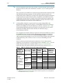
CPRI variations that provide a testbench. Refer to Chapter 8, Testbenches for
information about the specific testbench generated for each variation in Table 2–1.
Table 2–1. CPRI IP Core Variations that Provide a Demonstration Testbench
Properties
Common to all
Variations with
Testbench
REC master
clocking,
0.6144 Gbps line
rate (1), Include
HDLC Block is
Off, Enable MAP
interface
synchronization is
Off
Device Family
Arria II
Arria V,
Cyclone V,
Stratix V
Arria V (GT)
Cyclone IV GX,
Stratix IV GX
Enable
Autorate
Negotiation
Reference
Clock
Frequency
Include
MAC Block
Number of
Antenna-Carrier
Interfaces
Off
—
On or Off
3
Off
—
Off
0
On or Off
3
Off
0
On
0
Off
Off
61.44 MHz
On
On
0
Off
On
—
On or Off
3
Off
—
Off
0
On
—
On
0
Note to Table 2–1:
(1) Testbenches that exercise the autorate negotiation feature have different requirements for the starting CPRI line
rate of the DUT. Refer to Chapter 8, Testbenches.
CPRI MegaCore Function
User Guide
March 2013 Altera Corporation
Chapter 2: Getting Started
Integrating the CPRI IP Core in a Design
2–5
f For information about IP functional simulation models, refer to the Simulating Altera
Designs chapter in volume 3 of the Quartus II Handbook.
Integrating the CPRI IP Core in a Design
To compile the CPRI IP core and configure it on a device, you must integrate it in a
Quartus II project that provides additional functionality and constraints.
Supporting the Transceivers
When you integrate your CPRI IP core variation in your design, observe the following
connection requirements:
■
■
In Arria II, Cyclone IV GX, and Stratix IV GX designs:
■
Ensure that you connect the calibration clock (gxb_cal_blk_clk) to a clock
signal with the appropriate frequency range of 10–125 MHz. The cal_blk_clk
ports on other components that use transceivers must be connected to the same
clock signal.
■
Add a dynamic reconfiguration block (altgx_reconfig) and connect it as
specified in the Arria II Device Handbook, Cyclone IV Device Handbook, or
Stratix IV Device Handbook. This block supports offset cancellation to
compensate for analog voltages offset from required ranges due to process
variations. The design compiles without the altgx_reconfig block, but it
cannot function correctly in hardware.
■
To support the correct signal connections from the CPRI IP core to the dynamic
reconfiguration block, in the ALTGX MegaWizard Plug-In Manager, on the
Reconfiguration Settings tab, turn on Analog controls.
In Arria V, Cyclone V, and Stratix V designs, add an Altera Transceiver
Reconfiguration Controller and connect it as specified in the Altera Transceiver PHY
IP Core User Guide. This block supports offset cancellation to compensate for
analog voltages offset from required ranges due to process variations. The design
does compile without the Altera Transceiver Reconfiguration Controller, with a
critical warning, but it cannot function correctly in hardware.
Specifying Constraints
Altera provides a Synopsys Design Constraints (.sdc) file that you must apply to
ensure that the CPRI IP core meets design timing requirements. In most cases the
script requires modification for your design. For modification guidelines, refer to
Appendix E, Integrating the CPRI IP Core Timing Constraints in the Full Design.
In addition, before you compile your system to generate an SRAM Object File (.sof)
with which to configure your device, Altera recommends that you create assignments
for the high-speed transceiver VCCH settings.
To create assignments for the high-speed transceiver VCCH settings, perform the
following steps:
1. In the Quartus II window, on the Assignments menu, click Assignment Editor.
2. In the <<new>> cell in the To column, type the top-level signal name for your
CPRI IP core instance gxb_txdataout signal.
March 2013
Altera Corporation
CPRI MegaCore Function
User Guide
2–6
Chapter 2: Getting Started
Compiling and Programming the Device
3. Double-click in the Assignment Name column and click I/O Standard.
4. Double-click in the Value column and click your standard (for example, 1.5-V
PCML).
5. In the new <<new>> row, repeat steps 2 to 4 for your CPRI IP core instance
gxb_rxdatain signal.
f For information about timing analyzers, refer to the Quartus II Help and the “Timing
Analysis” section in volume 3 of the Quartus II Handbook.
Compiling and Programming the Device
You can use the Start Compilation command on the Processing menu in the
Quartus II software to compile your design. After successfully compiling your design,
program the targeted Altera device with the Programmer and verify the design in
hardware.
1
Before compiling your CPRI IP core or other incomplete CPRI design in the Quartus II
software, you must assign unconnected CPRI IP core signals to virtual pins.
f For information about compiling your design in the Quartus II software, refer to the
Quartus II Incremental Compilation for Hierarchical and Team-Based Design chapter in
volume 1 of the Quartus II Handbook. For information about programming an Altera
device, refer to the “Device Programming” section in volume 3 of the Quartus II
Handbook.
Instantiating Multiple CPRI IP Cores
If you want to instantiate multiple CPRI IP cores in an Arria II, Cyclone IV GX, or
Stratix IV GX device, to ensure your design optimizes its use of device pins, you must
observe the following additional requirements:
■
■
You must ensure that the gxb_cal_blk_clk input and gxb_powerdown signals are
connected according to the requirements for your target device family.
■
You must ensure that a single calibration clock source drives the
gxb_cal_blk_clk input to each CPRI IP core (or any other megafunction or
user logic that uses the ALTGX megafunction).
■
When you merge multiple CPRI IP cores in a single transceiver block, the same
signal must drive gxb_powerdown to each of the CPRI IP core variations and
other megafunctions, Altera IP cores, and user logic that use the ALTGX
megafunction.
You must ensure that the instances each have different starting channel numbers.
Multiple CPRI IP cores in a single device must use distinct transceiver channels.
You enforce this restriction by specifying different starting channel numbers for
the distinct CPRI IP cores. Refer to Chapter 3, Parameter Settings.
■
CPRI MegaCore Function
User Guide
To configure multiple CPRI IP cores in a single transceiver block, you must specify
in your Quartus Settings File (.qsf) that these CPRI link data lines are configured
March 2013 Altera Corporation
Chapter 2: Getting Started
Instantiating Multiple CPRI IP Cores
2–7
in the same GXB_TX_PLL_RECONFIG_GROUP, using the following syntax for each
outgoing CPRI link cN_gxb_txdataout:
set_instance_assignment -name GXB_TX_PLL_RECONFIG_GROUP 1 -to cN_gxb_txdataout
March 2013
Altera Corporation
CPRI MegaCore Function
User Guide
2–8
CPRI MegaCore Function
User Guide
Chapter 2: Getting Started
Instantiating Multiple CPRI IP Cores
March 2013 Altera Corporation
3. Parameter Settings
You customize the CPRI IP core by specifying parameters in the CPRI parameter
editor, which you access from the MegaWizard Plug-In Manager in the Quartus II
software.
This chapter describes the parameters and how they affect the behavior of the CPRI IP
core. You can modify parameter values to specify the following CPRI IP core
properties:
■
Default clocking mode—whether this CPRI IP core instance is configured initially
with slave clocking mode (RE slave) or with master clocking mode (REC or RE
master).
■
Line rate.
■
Autorate negotiation—whether this CPRI IP core instance supports the connection
of external logic to implement autorate negotiation.
■
Starting channel number.
■
Depth of the low-level receiver elastic buffer.
■
Transceiver reference clock frequency. This option is available only in Arria V,
Cyclone V, and Stratix V devices.
■
Ethernet MAC—whether to include an internal Ethernet MAC block or provide an
MII to connect to an external Ethernet module. These two options are mutually
exclusive.
■
HDLC block—whether to include an internal HDLC block or not.
■
Number of antenna-carrier interfaces.
■
Whether the antenna-carrier interfaces are clocked by the CPRI IP core clock
cpri_clkout or by external clocks.
Physical Layer Parameters
This section lists the parameters that affect the configuration of the physical layer of
the CPRI IP core.
Operation Mode Parameter
The Operation mode parameter specifies whether the CPRI IP core is configured with
slave clocking mode or with master clocking mode. An REC is configured with master
clocking mode.
The value of this parameter determines the initial operation mode of the CPRI IP core.
You can modify the IP core operation mode dynamically by modifying the value of
the operation_mode bit of the CPRI_CONFIG register (Table 7–6 on page 7–4).
In your design, you must connect the clocks appropriately for the operation mode.
Refer to “Clock Diagrams for the CPRI IP Core” on page 4–5.
March 2013
Altera Corporation
CPRI MegaCore Function
User Guide
3–2
Chapter 3: Parameter Settings
Physical Layer Parameters
For information about how to dynamically switch the clock mode of your CPRI IP
core, refer to “Dynamically Switching Clock Mode” on page 4–9.
Line Rate Parameter
The Line rate parameter specifies the line rate on the CPRI link in gigabits per second
(Gbps). Table 3–1 lists the CPRI line rates that each device family supports. A
checkmark indicates a supported variation.
Table 3–1. Device Family Support for CPRI Line Rates (1)
Device Family
or Variant
CPRI Line Rate (Gbps)
0.6144
1.2288
2.4576
3.072
4.9152
6.144
9.8304
Arria II GX
v
v
v
v
v
v
—
Arria II GZ
v
v
v
v
v
v
—
Arria V GX
v
v
v
v
v
v
—
Arria V GT
v
v
v
v
v
v
v
Arria V GZ
v
v
v
v
v
v
v
Cyclone IV GX
v
v
v
v
—
—
—
Cyclone V GX
v
v
v
v
—
—
—
Stratix IV GX
v
v
v
v
v
v
—
Stratix V GX
v
v
v
v
v
v
v
Stratix V GT
v
v
v
v
v
v
v
Note to Table 3–1:
(1) Refer to Table 1–4 on page 1–8 for information about the device speed grades that support each CPRI line rate.
The parameter editor does not enforce these restrictions. However, if you target a device whose speed grade does
not support the CPRI line rate you configure, compilation fails because the design cannot meet timing in hardware.
Enable Autorate Negotiation
Autorate negotiation is the process of stepping down from a higher target CPRI line
rate to a lower target CPRI line rate if you are unable to establish a link at the higher
line rate. If your CPRI IP core has autorate negotiation enabled, and you program it to
step down from its highest target CPRI line rate to its lower target CPRI line rates
when it does not achieve frame synchronization, your CPRI IP core achieves frame
synchronization at the highest possible CPRI line rate in its range of potential line
rates, depending on the capability of its CPRI partner.
For information about the autorate negotiation feature, refer to Appendix B,
Implementing CPRI Link Autorate Negotiation.
Turn on the Enable auto-rate negotiation parameter to specify that your CPRI IP core
supports autorate negotiation. By default, this parameter is turned off.
Transceiver Starting Channel Number
You can specify the starting number for the CPRI IP core transceiver. For a CPRI IP
core master, the Master transceiver starting channel number specifies the starting
channel number for the transceiver.
CPRI MegaCore Function
User Guide
March 2013 Altera Corporation
Chapter 3: Parameter Settings
Physical Layer Parameters
3–3
For a CPRI IP core configured with slave clocking mode, the Slave transmitter
starting channel number and Slave receiver starting channel number are two
separate parameters. Both must have values that are starting channel numbers
available in your design. The two numbers must be different but the Quartus II
software creates an FPGA configuration with a single slave transceiver.
If you instantiate multiple CPRI IP cores on the same device, you must ensure each
uses distinct transceiver channels.
These parameters are not available in Arria V, Cyclone V, and Stratix V devices.
Rx Elastic Buffer Depth
You can specify the depth of the Rx elastic buffer in the CPRI Receiver block. The
Receiver buffer depth value is the log2 of the Rx elastic buffer depth. Allowed values
are 4 to 8, inclusive.
The default depth of the Rx elastic buffer is 64, specified by the Receiver buffer depth
parameter default value of 6. For most systems, the default Rx elastic buffer depth is
adequate to handle dispersion, jitter, and drift that can occur on the link while the
system is running. However, the parameter is available for cases in which additional
depth is required.
1
Altera recommends that you set Receiver buffer depth to 4 in CPRI RE slave
variations.
CPRI IP core variations configured at a CPRI line rate of 9830.4 Mbps that target an
Arria V GT device do not include an Rx elastic buffer. However, this parameter affects
the depth of the RX buffer between the soft PCS and the Altera Transceiver Native
PHY IP core, instead. Refer to Figure 4–4 on page 4–8 and Figure 4–5 on page 4–9.
f For information about the Altera Transceiver Native PHY IP core, refer to the Altera
Transceiver PHY IP Core User Guide.
The value you specify for Receiver buffer depth is referred to as WIDTH_RX_BUF in
this user guide.
For more information about the Rx elastic buffer, refer to “Rx Elastic Buffer” on
page 4–54.
Transceiver Reference Clock Frequency
If your CPRI variation targets an Arria V, Cyclone V, or Stratix V device, the
Transceiver reference clock frequency parameter is available. Use this parameter to
modify the expected frequency of the CPRI transceiver input reference clock to the
frequency of an available clock for your design.
The frequency you specify is an input parameter to the Altera Deterministic Latency
PHY IP core that is included in your Arria V, Cyclone V, or Stratix V CPRI variation.
Values available at each CPRI line rate are the reference clock frequencies for which
the Deterministic Latency PHY IP core supports the target CPRI line rate. The default
value is 122.88 MHz.
March 2013
Altera Corporation
CPRI MegaCore Function
User Guide
3–4
Chapter 3: Parameter Settings
Data Link Layer Parameters
In the case of an Arria V GT variation configured with CPRI line rate 9830.4 Mbps, the
frequency is an input parameter to the Altera Native PHY IP core.
f For more information about the Altera Deterministic Latency PHY IP core and the
Altera Native PHY IP core, refer to the Altera Transceiver PHY IP Core User Guide.
Data Link Layer Parameters
This section lists the parameter that affects the configuration of the data link layer of
the CPRI IP core.
Include MAC Block
Turn on the Include MAC block parameter to specify that your CPRI IP core includes
an internal Ethernet MAC block. By default, this parameter is turned off. If this
parameter is turned off, the CPRI IP core implements the media-independent
interface (MII) to your own external Ethernet MAC, instead.
If this parameter is turned off in your CPRI IP core, your application cannot access the
Ethernet registers. Attempts to access these registers read zeroes and do not write
successfully, as for a reserved register address.
For information about the internal Ethernet MAC block, refer to “Accessing the
Ethernet Channel” on page 4–47.
For information about the MII, refer to “Media Independent Interface to an External
Ethernet Block” on page 4–37.
Include HDLC Block
Turn on the Include HDLC block parameter to specify that your CPRI IP core
includes an internal HDLC block. By default, this parameter is turned off.
If this parameter is turned off in your CPRI IP core, your application cannot access the
HDLC registers. Attempts to access these registers read zeroes and do not write
successfully, as for a reserved register address.
For information about the HDLC block, refer to “Accessing the HDLC Channel” on
page 4–50.
Application Layer Parameters
This section lists the parameters that affect the configuration of the application layer
of the CPRI IP core.
CPRI MegaCore Function
User Guide
March 2013 Altera Corporation
Chapter 3: Parameter Settings
Application Layer Parameters
3–5
Mapping Mode
The Mapping mode(s) parameter specifies whether your CPRI IP core MAP interface
supports a programmable AxC mapping mode or is configured with a specific
mapping mode. Table 3–2 lists the supported values.
Table 3–2. MAP Interface AxC Mapping Mode Support
Value
Description
If you select this value, you configure a CPRI IP core which you can program
dynamically to be in any mapping mode. In this case, you determine the current
mapping mode for your CPRI IP core by programming the map_mode field of the
CPRI_MAP_CONFIG register (0x100).
All
For backward compatibility with previous releases of the CPRI IP core, the value of
All is the default value for this parameter.
For information about the map_mode register field, refer to Table 7–31 on
page 7–15.
Your CPRI IP core MAP interface is configured to function in basic mapping mode
only. This mapping mode has the following features:
Basic
■
Conforms to the description in Sections 4.2.7.2.2 and 4.2.7.2.3 of the CPRI
Specification V4.2 Interface Specification.
■
Supports communication that complies with the LTE/E-UTRA or UMTS/WCDMA
standard.
For information about the basic mapping mode in the CPRI IP core, refer to “MAP
Interface Mapping Modes” on page 4–13.
Your CPRI IP core MAP interface is configured in a single AxC mapping mode only,
a mode that has the following features:
■
Conforms to Method 1: IQ Sample Based described in Section 4.2.7.2.5 of the
CPRI Specification V4.2 Interface Specification.
■
Supports communication that complies with the WiMAX standard.
Advanced 1
For information about this AxC mapping mode, refer to Appendix C, Advanced AxC
Mapping Modes.
Your CPRI IP core MAP interface is configured in a single AxC mapping mode only,
a mode that has the following features:
Advanced 2
■
Conforms to Method 3: Backward Compatible described in Section 4.2.7.2.4 of
the CPRI Specification V4.2 Interface Specification.
■
Supports communication that complies with the WiMAX or LTE/E-UTRA
standard.
For information about this AxC mapping mode, refer to Appendix C, Advanced AxC
Mapping Modes.
Your CPRI IP core MAP interface is configured in a single AxC mapping mode only,
a legacy mode that has the following features:
Advanced 3
■
Conforms to Method 1: IQ Sample Based described in Section 4.2.7.2.5 of the
CPRI Specification V4.2 Interface Specification.
■
Supports communication that complies with the LTE/E-UTRA standard.
This mode does not support 16-bit wide IQ data samples. Refer to Table 7–31 on
page 7–15.
For information about this AxC mapping mode, refer to Appendix C, Advanced AxC
Mapping Modes.
March 2013
Altera Corporation
CPRI MegaCore Function
User Guide
3–6
Chapter 3: Parameter Settings
Application Layer Parameters
Number of Antenna-Carrier Interfaces
The Number of antenna/carrier interfaces parameter specifies the number of
antenna-carrier interfaces, or data channels, in your CPRI IP core. The supported
values are 0 to 24. Set this parameter to the maximum number of data channels you
expect your CPRI IP core to use at the same time.
If this parameter has the value of zero, your CPRI IP core does not implement the
CPRI MAP interface. For example, you might use this option if your CPRI IP core
passes IQ data samples through the AUX interface to an external custom mapping
function that you provide. The default value of this parameter is zero.
The combination of CPRI IP core line rate, sampling width, and sampling rate restricts
the number of active antenna-carrier interfaces your CPRI IP core can support. For
example, if your CPRI IP core operates at line rate 3.072 Gbps, it can support as many
as 20 active antenna-carrier interfaces, but if your CPRI IP core operates at line rate
1.2288 Gbps, it can support a maximum of eight active antenna-carrier interfaces. For
details, refer to Table 4–5 and Table 4–6 on page 4–17.
You can specify in software that some of the antenna-carrier interfaces that you
configure in your CPRI IP core are not active. This feature allows you to change the
number of active and enabled data channels dynamically.
1
The software configuration feature allows you to modify the number of active
antenna-carrier interfaces. If you modify this number, you must keep in mind the
restrictions for your current CPRI line rate. Otherwise, data is dropped in the
mapping to and from the individual antenna-carrier interfaces.
If you set the map_ac field of the CPRI_MAP_CNT_CONFIG register to a number N that is
lower than the value you specify for Number of antenna/carrier interfaces, then the
first N data channels are active and the others are not. In addition, for each
antenna-carrier interface you can use the relevant map_rx_enable bit of the
CPRI_IQ_RX_BUF_CONTROL register and the relevant map_tx_enable bit of the
CPRI_IQ_TX_BUF_CONTROL register to enable or disable the specific data channel and
direction. A data channel must be configured, active, and enabled to function. If it is
configured and active but not enabled, or if it is configured but not active, data to and
from it is ignored.
The value you specify for Number of antenna/carrier interfaces is referred to as
N_MAP in this user guide.
For more information about the antenna-carrier interfaces in a CPRI IP core, refer to
“MAP Interface” on page 4–12.
Enable Internally-Clocked Synchronization Mode
If you configure one or more antenna-carrier interfaces, the option to Enable MAP
interface synchronization with core clock is available. If you turn on this option, both
the MAP receiver interface and the MAP transmitter interface are clocked with the
CPRI IP core internal clock, cpri_clkout. If you turn off this option, these interfaces
are clocked with individual Rx and Tx clocks for each antenna-carrier interface. By
default, this option is turned off.
CPRI MegaCore Function
User Guide
March 2013 Altera Corporation
Chapter 3: Parameter Settings
Application Layer Parameters
3–7
If you turn on this option, the CPRI IP core coordinates communication on these
interfaces in the internally-clocked synchronization mode. Turning on this option
simplifies synchronization of data transfers to and from the antenna-carrier interfaces.
The Boolean value you specify for Enable MAP interface synchronization with core
clock is referred to as SYNC_MAP in this user guide. Table 3–3 shows the
correspondence between the parameter, the MAP interface synchronization mode,
and the clocks that clock the antenna-carrier interfaces.
Table 3–3. Meaning of Enable Map Interface synchronization with core clock Parameter
Enable MAP interface
SYNC_MAP
synchronization with core clock
MAP Interface
Synchronization Mode
Clocks for Antenna-Carrier Interfaces
On
1
Internally-clocked mode cpri_clkout
Off
0
Synchronous buffer or
FIFO mode
mapN_rx_clk, mapN_tx_clk, for
antenna-carrier interfaces N = 1 ... (N_MAP – 1)
For more information about these clocks, refer to “Clocking Structure” on page 4–3.
For more information about the synchronization modes for the Rx and Tx MAP
interfaces, and how they vary depending on your selection of this option, refer to
“MAP Interface” on page 4–12.
March 2013
Altera Corporation
CPRI MegaCore Function
User Guide
3–8
Chapter 3: Parameter Settings
Application Layer Parameters
CPRI MegaCore Function
User Guide
March 2013 Altera Corporation
4. Functional Description
The CPRI protocol interface complies with the CPRI Specification V5.0. The
specification divides the protocol into a two-layer hierarchy: a physical layer (layer 1)
and a data link layer (layer 2). The specification describes the following three
communication planes:
■
User data
■
Control and management (C&M)
■
Timing synchronization information
f More detailed information about the CPRI specification is available from the CPRI
website at www.cpri.info.
The Altera CPRI IP core implements layer 1 and layer 2 of the specification in the
CPRI protocol interface module. This chapter describes the individual data and
control interfaces available to you and how the data on these interfaces is loaded and
unloaded from the CPRI frame.
This chapter contains the following sections:
■
Architecture Overview
■
Clocking Structure
■
Reset Requirements
■
MAP Interface
■
Auxiliary Interface
■
Media Independent Interface to an External Ethernet Block
■
CPU Interface
■
March 2013
Altera Corporation
■
Accessing the Hyperframe Control Words
■
Accessing the Ethernet Channel
■
Accessing the HDLC Channel
CPRI Protocol Interface Layer (Physical Layer)
CPRI MegaCore Function
User Guide
4–2
Chapter 4: Functional Description
Architecture Overview
Architecture Overview
Figure 4–1 shows the main blocks of the CPRI IP core.
Figure 4–1. CPRI IP Core Block Diagram
IQ Data Channels
(Optional)
AxC
IF
1
(1)
...
AxC
IF
24
(1)
CPRI MAP
Interface Module
MI Interface
CPU Interface
MII
(2)
CPU Interface Module
Control and Management
Module
Ethernet
(2)
VSS/
Inband/
Alarms
RX Delay Measurement
and TX Calibration
Block
AUX Interface
AUX
Module
Registers
HDLC
(3)
Physical Layer
Transmitter
Receiver
Transmitter
Transceiver
Receiver
Transceiver
tx_dataout
rx_datain
CPRI Link
CPRI Link
Notes to Figure 4–1:
(1) You can configure your CPRI IP core with zero, one, or multiple IQ data channels.
(2) You can configure your CPRI IP core with an Ethernet MAC block or an MII block. The two options are mutually exclusive.
(3) You can configure your CPRI IP core with or without an HDLC block.
The Altera CPRI IP core supports the following interfaces:
■
MAP Interface
■
Auxiliary Interface
■
Media Independent Interface to an External Ethernet Block
■
CPU Interface
■
CPRI link interface described in CPRI Protocol Interface Layer (Physical Layer)
Information about the signals on the individual interfaces is available in the following
sections and in Chapter 6, Signals.
The following sections describe the individual interfaces and clocks.
CPRI MegaCore Function
User Guide
March 2013 Altera Corporation
Chapter 4: Functional Description
Clocking Structure
4–3
Clocking Structure
The CPRI IP core has a variable number of clock domains. The clock domains in your
CPRI IP core variation depend on the following factors:
■
Number of antenna-carrier interfaces.
■
Whether the MII is configured.
■
Whether the antenna-carrier interfaces are clocked internally. Refer to “Enable
Internally-Clocked Synchronization Mode” on page 3–6.
■
Target device family.
■
In one case, different CPRI line rates.
The input clock frequency requirements depend on the target device family and CPRI
line rate. Refer to Table 4–2 on page 4–10 for these requirements.
You can configure a CPRI IP core in master or slave clocking mode, as described in
“Operation Mode Parameter” on page 3–1. REC configurations and RE master
configurations use master clocking mode, and RE slave configurations use slave
clocking mode. Your design must handle some of the transceiver input clocks
differently in the two different clocking modes. The clocking diagrams in “Clock
Diagrams for the CPRI IP Core” on page 4–5 describe the requirements.
The CPRI IP core supports dynamic switching between master and slave clocking
modes. This section describes how to connect the CPRI IP core input clock signals to
support dynamic clock mode switching and how to dynamically switch the clock
mode in your CPRI IP core.
Table 4–1 describes the individual clocks. The clocking diagrams in Figure 4–2 on
page 4–6 to Figure 4–4 on page 4–8 show the clocks and clock domain boundaries.
Table 4–2 on page 4–10 lists the clock frequencies for the different CPRI IP core
variations.
CPRI IP Core Clocks
Table 4–1 describes the clock domains in the CPRI IP core.
For more information about these clocks, including driver requirements, refer to
Chapter 6, Signals. For expected input clock frequencies refer to Chapter 6, Signals
and to Table 4–2 on page 4–10.
Table 4–1. CPRI IP Core Clocks (Part 1 of 3)
Clock Name
cpri_clkout
March 2013
Direction
Output
Altera Corporation
Configuration
Requirements
Present in all
CPRI IP cores
Description
Main clock for the CPRI IP core. The CPRI IP core derives this clock
from the transceiver transmit PLL, and the frequency of this clock
depends on the CPRI line rate. For more information refer to “CPRI
Communication Link Line Rates” on page 4–10.
CPRI MegaCore Function
User Guide
4–4
Chapter 4: Functional Description
Clocking Structure
Table 4–1. CPRI IP Core Clocks (Part 2 of 3)
Clock Name
mapN_tx_clk
for N in
0..(N_MAP–1)
Direction
Input
mapN_rx_clk
for N in
0..(N_MAP–1)
Input
clk_ex_delay
Input
cpri_mii_txclk
cpri_mii_rxclk
Output
Output
Configuration
Requirements
Description
Present in
variations
configured with
N_MAP > 0
antenna-carrier
interfaces and
with Enable MAP
interface
synchronization
with core clock
turned off
Expected rate of received data on antenna-carrier interface N. The
frequency of this clock is the sample rate on the incoming
antenna-carrier interface. For more information about data channel
sample rates, refer to Table 4–5 and Table 4–6 on page 4–17.
Present in all
CPRI IP cores
Clock for extended delay measurement. For more information refer to
“Extended Rx Delay Measurement” on page D–7.
Present in
variations
configured with
an MI interface
Clocks the transmissions of antenna-carrier interface N. The
frequency of this clock is the sample rate on the outgoing
antenna-carrier interface. For more information about data channel
sample rates, refer to Table 4–5 and Table 4–6 on page 4–17.
Clocks the MII transmitter module. This clock has the same
frequency as the cpri_clkout clock. The frequency depends on the
CPRI line data rate. Refer to “CPRI Communication Link Line Rates”
on page 4–10.
Clocks the MII receiver module. This clock has the same frequency as
the cpri_clkout clock. The frequency depends on the CPRI line
data rate. Refer to “CPRI Communication Link Line Rates” on
page 4–10.
Present in all
CPRI IP cores
Controls the input to the CPU interface of the CPRI IP core and drives
the CPU interface. Assumed to be asynchronous with the
cpri_clkout clock. The maximum frequency is constrained by fMAX
and can vary based on the device family and speed grade.
Input
Present in all
CPRI IP cores
Reference clock for the transceiver PLLs. In master clocking mode,
this clock drives both the receiver PLL and the transmitter PLL in the
transceiver. In slave clocking mode, this clock drives the receiver
PLL.
In master clocking mode, you must tie this input to the same source
as gxb_pll_inclk.
gxb_cal_blk_clk
Input
Not present in
variations that
target an Arria V,
Cyclone V, or
Stratix V device
Transceiver calibration-block clock.
reconfig_clk
Input
Present in all
CPRI IP cores
Transceiver dynamic reconfiguration block clock.
gxb_pll_inclk
Input
Present in all
CPRI IP cores
Input clock to the transmitter PLL in a CPRI IP core configured in
slave clocking mode. In master clocking mode, you must tie this
input to the same source as gxb_refclk.
Output
Present in all
CPRI IP cores
Generated from transceiver clock data recovery circuit. Intended to
connect to an external PLL for jitter clean-up in slave clocking mode.
cpu_clk
gxb_refclk
pll_clkout
CPRI MegaCore Function
User Guide
Input
March 2013 Altera Corporation
Chapter 4: Functional Description
Clocking Structure
4–5
Table 4–1. CPRI IP Core Clocks (Part 3 of 3)
Clock Name
Direction
usr_pma_clk
Input
usr_clk
Input
Configuration
Requirements
Present in
variations
configured at
9830.4 Gbps that
target an
Arria V GT device
Description
Extra clock signal required to drive the PMA in these CPRI IP core
variations. Refer to Table 6–15 on page 6–17 for driver frequency and
synchronization requirements.
Extra clock signal required to drive the PCS in these CPRI IP core
variations. Refer to Table 6–15 on page 6–17 for driver frequency and
synchronization requirements.
Clock Diagrams for the CPRI IP Core
Figure 4–2 and Figure 4–3 show the clocking schemes for CPRI IP cores configured as
RE slaves, RE masters, and REC masters that do not target an Arria V GT device or
that are not configured with a CPRI line rate of 9830.4 Mbps.
Figure 4–4 on page 4–8 and Figure 4–5 on page 4–9 show the clocking schemes for
CPRI IP cores configured as RE slaves, RE masters, and REC masters with a CPRI line
rate of 9830.4 Mbps that target an Arria V GT device. These variations have no clock
divider and no Tx elastic buffer or Rx elastic buffer. However, they require two
additional synchronized input clocks, usr_pma_clk and usr_clk.
You must drive the usr_pma_clk and usr_clk clocks at the , which you must drive at
the frequency of 122.88 MHz, and usr_clk, which you must drive at the frequency of
245.76 MHz.
March 2013
Altera Corporation
CPRI MegaCore Function
User Guide
4–6
Chapter 4: Functional Description
Clocking Structure
Clock Diagrams for Most CPRI IP Core Variations
Figure 4–2 shows the clock diagram for a CPRI IP core configured as an RE slave,
unless the IP core is configured with CPRI line rate 9.830.4 Mbps and targets an
Arria V GT device.
Figure 4–2. CPRI IP Core Slave Clocking Except for Arria V GT 9.8 Gbps Variations
gxb_refclk
cpri_clkout
CPRI MegaCore Function
cpri_clkout
Clock
Domain
Tx Elastic
Sync Buffer
CPRI Tx
MAP
Interface
FIFO
Buffer
mapN_tx_clk
cpri_mii_txclk
Clock
Divider
(1)
tx_clkout
Transceiver
CPRI TX
MII Interface
cpri_mii_rxclk
cpu_clk
CPU
Interface
CPRI RX
CDR
rx_clkout
Rx Elastic
Sync Buffer
pll_clkout
gxb_pll_inclk
FIFO
Buffer
mapN_rx_clk
CPRI Rx
MAP
Interface
clk_ex_delay
Clean-Up PLL
Note to Figure 4–2:
(1) The clock divider factor depends on the device family. In device families with a factor of 1, the divider is not configured. Table 4–17 on page 4–59
lists the datapath width and clock divider by device family.
CPRI MegaCore Function
User Guide
March 2013 Altera Corporation
Chapter 4: Functional Description
Clocking Structure
4–7
Figure 4–3 shows the clock diagram for a CPRI IP core configured as an REC master
or as an RE master, unless the IP core is configured with CPRI line rate 9830.4 Mbps
and targets an Arria V GT device.
Figure 4–3. CPRI IP Core Master Clocking Except for Arria V GT 9.8 Gbps Variations
gxb_refclk
gxb_pll_inclk
cpri_clkout
CPRI MegaCore Function
cpri_clkout
Clock
Domain
Tx Elastic
Sync Buffer
CPRI Tx
MAP
Interface
FIFO
Buffer
mapN_tx_clk
cpri_mii_txclk
tx_clkout
Transceiver
Clock
Divider
(1)
CPRI TX
cpri_mii_rxclk
cpu_clk
CPRI RX
CDR
MII Interface
rx_clkout
Rx Elastic
Sync Buffer
pll_clkout
CPU
Interface
FIFO
Buffer
mapN_rx_clk
CPRI Rx
MAP
Interface
clk_ex_delay
Note to Figure 4–3:
(1) The clock divider factor depends on the device family. In device families with a factor of 1, the divider is not configured. Table 4–17 on page 4–59
lists the datapath width and clock divider by device family.
Clock Diagrams for CPRI IP Core Arria V GT Variations at 9830.4 Mbps
CPRI IP core variations configured with a CPRI line rate of 9830.4 Mbps that target an
Arria V GT device have a different clocking scheme. These variations have no clock
divider, and have neither an RX elastic buffer nor a TX elastic buffer.
These variations use two additional input clock signals, usr_clk and usr_pma_clk.
Table 6–15 on page 6–17 describes the requirements for these two input clock signals.
When a variation configured with a CPRI line rate of 9830.4 Mbps that targets an
Arria V GT device participates in autorate negotiation, you must modify the
frequency of the usr_clk and usr_pma_clk input clocks to specific values for the
different CPRI line rates. Refer to Appendix B, Implementing CPRI Link Autorate
Negotiation.
March 2013
Altera Corporation
CPRI MegaCore Function
User Guide
4–8
Chapter 4: Functional Description
Clocking Structure
Figure 4–4 shows the clocking scheme for a CPRI IP core that targets an Arria V GT
device and is configured with a CPRI line rate of 9830.4 Mbps, configured or
programmed as an RE slave.
Figure 4–4. CPRI IP Core Slave Clocking in Arria V GT 9.8 Gbps Variations (1)
gxb_refclk
usr_pma_clk
(122.88 MHz)
tx_clkout
122.88 MHz
usr_clk
(245.76 MHz)
cpri_clkout
CPRI MegaCore Function
cpri_clkout
Clock
Domain
tx_clkout
80
TX
Buffer
80
Soft
PCS
FIFO
Buffer
32
Transceiver
Native PHY
IP Core
32
80
RX
Buffer
rx_clkout
MII Interface
CPU
Interface
Soft
PCS
data
FIFO
Buffer
cpu_clk
mapN_rx_clk
CPRI Rx
MAP
Interface
122.88 MHz
pll_clkout
cpri_mii_rxclk
CPRI RX
32
32
gxb_pll_inclk
mapN_tx_clk
cpri_mii_txclk
data
CPRI TX
80
CPRI Tx
MAP
Interface
clk_ex_delay
Clean-Up PLL
Notes to Figure 4–4:
(1) In slave clocking mode, the usr_clk and usr_pma_clk input clocks must be driven by a common source from the cleanup PLL. For additional
constraints these clocks require, refer to Table 6–15 on page 6–17.
CPRI MegaCore Function
User Guide
March 2013 Altera Corporation
Chapter 4: Functional Description
Clocking Structure
4–9
Figure 4–5 shows the clocking scheme for a CPRI IP core that targets an Arria V GT
device and is configured with a CPRI line rate of 9830.4 Mbps, configured or
programmed as an REC or RE master.
Figure 4–5. CPRI IP Core Master Clocking in Arria V GT 9.8 Gbps Variations (1)
gxb_refclk
usr_pma_clk
(122.88 MHz)
gxb_pll_inclk tx_clkout
122.88 MHz
usr_clk
(245.76 MHz)
cpri_clkout
CPRI MegaCore Function
cpri_clkout
Clock
Domain
tx_clkout
80
TX
Buffer
80
Soft
PCS
32
rx_clkout
cpri_mii_txclk
data
CPRI TX
80
80
RX
Buffer
mapN_tx_clk
FIFO
Buffer
32
Transceiver
Native PHY
IP Core
CPRI Tx
MAP
Interface
MII Interface
CPU
Interface
Soft
PCS
cpu_clk
CPRI RX
32
32
data
mapN_rx_clk
FIFO
Buffer
CPRI Rx
MAP
Interface
122.88 MHz
pll_clkout
cpri_mii_rxclk
clk_ex_delay
Notes to Figure 4–5:
(1) In master clocking mode, you must drive the gxb_pll_inclk and gxb_refclk input signals from a common source.
Dynamically Switching Clock Mode
The CPRI IP core supports dynamic clock mode switching, from master clock mode to
slave clock mode and from slave clock mode to master clock mode. The value you
select for Operation mode in the CPRI parameter editor determines the clock mode in
which the IP core is configured initially. However, you can modify this value
dynamically.
To switch the clock mode of your CPRI IP core, perform the following steps:
1. Ensure your design supports the input clock connection requirements for the clock
mode to which you intend to switch the IP core.
2. Implement the clock connection requirements for the intended new clock mode by
switching the source that drives the gxb_pll_inclk signal. Refer to “Clock
Diagrams for the CPRI IP Core” on page 4–5.
3. Write the new value to the operation_mode bit of the CPRI_CONFIG register. Refer to
Table 7–6 on page 7–4 for the appropriate value.
4. Wait until you observe successful CPRI link resynchronization. Refer to
Appendix A, Initialization Sequence.
March 2013
Altera Corporation
CPRI MegaCore Function
User Guide
4–10
Chapter 4: Functional Description
Clocking Structure
CPRI Communication Link Line Rates
The CPRI specification specifies line rates of n × 614.4 Mbps for various values of n.
The CPRI IP core supports different ranges of line rates in different device families.
Table 3–1 on page 3–2 lists the CPRI line rate support available in the different device
families.
Table 4–2 shows the relationship between line rates, default transceiver reference
clock (gxb_refclk) rates, parallel recovered clock (pll_clkout) rates, and internal
clock (cpri_clkout) rates.
Table 4–2. CPRI Link Line Rates and Clock Rates for CPRI MegaCore Function
(1)
Clock Frequency (MHz)
pll_clkout Frequency
(If line rate is supported)
Default gxb_refclk Frequency
(If line rate is supported)
Line Rate
(Mbps)
cpri_clkout
Arria V GX
Frequency
Arria V
Arria II GX
Arria II GZ
Arria II GX
Arria II GZ
Arria V GZ
(If
line
rate
Cyclone V
and
and
and
and
Cyclone V Arria V GT
is
and
Cyclone IV GX Stratix IV GX
Cyclone IV GX Stratix IV GX
and
Devices
Stratix V supported)
Devices
Devices
Stratix V
Devices
Devices
Devices
Devices
614.4
61.44
61.44
15.36
61.44
61.44
15.36
15.36
1228.8
61.44
61.44
30.72
61.44
30.72
30.72
30.72
2457.6
122.88
61.44
61.44
122.88
61.44
61.44
61.44
(2)
3072
153.60
76.80
76.80
153.60
76.80
76.80
76.80
4915.2 (3)
245.76
122.88
122.88
245.76
122.88
122.88
122.88
6144 (3)
307.20
153.60
153.60
307.20
153.60
153.60
153.60
9830.4 (4)
—
—
245.76
—
—
245.76
122.88
Notes to Table 4–2:
(1) In this table, device families can be grouped with other device families that do not support all of the same CPRI line rates. The values apply only for
supported CPRI line rates for each device family.
(2) The value of gxb_refclk in CPRI IP cores that target a 28-nm device (Arria V, Cyclone V, or Stratix V device) is the Transceiver reference clock
frequency parameter value that you set in the CPRI parameter editor.
(3) The CPRI IP core does not support CPRI line rates 4915.2 Mbps and 6144 Mbps in variations that target Cyclone IV GX or Cyclone V GX devices.
(4) The CPRI IP core supports CPRI line rate 9830.4 Mbps in variations that target Stratix V (GX or GT), Arria V GT, or Arria V GZ devices. The CPRI IP
core does not support CPRI line rate 9830.4 Mbps for any other devices, including Arria V GX devices.
The cpri_clkout frequency depends only on the CPRI line rate. The pll_clkout
frequency depends on the CPRI line rate and on the datapath width through the
transceiver, except in Arria V, Cyclone V, and Stratix V devices. The datapath width is
determined by device family, as shown in Table 4–17 on page 4–59.
The gxb_refclk clock is the incoming reference clock for the device transceiver’s PLL.
Altera allows you to program the transceiver to work with any of a set of gxb_refclk
frequencies that the PLL in the transceiver can convert to the required internal clock
speed for the CPRI IP core line rate. The parameter editor in which you configure the
gxb_refclk frequency depends on the target device family for your CPRI IP core
variation.
CPRI MegaCore Function
User Guide
March 2013 Altera Corporation
Chapter 4: Functional Description
Reset Requirements
4–11
When you generate a CPRI IP core variation that targets an Arria II, Cyclone IV GX, or
Stratix IV GX device, you generate an ALTGX megafunction with specific default
settings. These default transceiver settings configure a transceiver that works
correctly with the CPRI IP core when the input gxb_refclk clock has the frequency
shown in Table 4–2. However, you can edit the ALTGX megafunction instance to
specify a different gxb_refclk frequency that is more convenient for your design, for
example, to enable you to use an existing clock in your system as the gxb_refclk
reference clock.
When you generate a CPRI IP core variation that targets an Arria V, Cyclone V, or
Stratix V device, you generate an Altera Deterministic Latency PHY IP core or Altera
Native PHY IP core with specific default settings. However, you set the gxb_refclk
frequency in the CPRI parameter editor. As described in Chapter 3, Parameter
Settings, for these target devices the CPRI parameter editor provides a list of potential
transceiver reference clock frequencies from which you select the frequency that is
most convenient for your design.
Reset Requirements
The CPRI IP core has multiple independent reset signals.To reset the CPRI IP core
completely, you must assert all the reset signals.
You can assert all reset signals asynchronously to any clock. However, each reset
signal must be asserted for at least one full clock period of a specific clock, and be
deasserted synchronously to the rising edge of that clock. For example, the CPU
interface reset signal, cpu_reset, must be deasserted on the rising edge of cpu_clk.
Table 4–3 lists the reset signals and their corresponding clock domains.
Table 4–3. Reset Signals and Corresponding Clock Domains
Reset Signal
reset
Clock Domain
reconfig_clk
—
gxb_powerdown
March 2013
Description
Resets the CPRI protocol interface. Drives the
reset controller.
Powers down and resets the high-speed
transceiver block. For setup and hold times,
refer to the relevant device handbook. This
signal is not present in CPRI IP core variations
that target an Arria V, Cyclone V, or Stratix V
device.
reset_ex_delay
clk_ex_delay
Resets the extended delay measurement block.
config_reset
cpri_clkout
Resets the registers to their default values.
cpu_reset
cpu_clk
Resets the CPU interface.
mapN_rx_reset
mapN_rx_clk
Resets the MAP Channel N receiver block in
FIFO or synchronous buffer MAP
synchronization mode.
mapN_tx_reset
mapN_tx_clk
Resets the MAP Channel N transmitter block in
FIFO or synchronous buffer MAP
synchronization mode.
Altera Corporation
CPRI MegaCore Function
User Guide
4–12
Chapter 4: Functional Description
MAP Interface
You must implement logic to ensure the minimal hold time and synchronous
deassertion of each reset input signal to the CPRI IP core. Figure 4–6 shows a circuit
that ensures these conditions for one reset signal.
Figure 4–6. Circuit to Ensure Synchronous Deassertion of Reset Signal
rst
CPRI
MegaCore
Function
rst
D
rst
Q
D
Q
reset
clk
For more information about the requirements for reset signals, refer to Chapter 6,
Signals.
The CPRI IP core has a dedicated reset control module to enforce the specific reset
requirements of the high-speed transceiver module. This reset controller generates the
recommended reset sequence for the transceiver. The reset signal controls the reset
control module.
In Arria V, Cyclone V, and Stratix V devices, the Altera Deterministic Latency PHY IP
core or Altera Native PHY IP core that is generated with the CPRI IP core implements
the reset controller. In earlier device families, the reset control module is internal to
the CPRI IP core, but external to the ALTGX megafunction instance generated with
the CPRI IP core.
After reset, your software must perform link synchronization and other initialization
tasks. For information about the required initialization sequence following CPRI IP
core reset, refer to Appendix A, Initialization Sequence.
MAP Interface
The CPRI IP core MAP interface comprises the individual antenna-carrier interfaces,
or data channels, through which the CPRI IP core transfers IQ sample data to and
from the RF implementation. The MAP interface is implemented as an incoming and
an outgoing Avalon-ST interface. The Avalon-ST interface provides a standard,
flexible, and modular protocol for data transfers from a source interface to a sink
interface.
f For information about the Avalon-ST interface, refer to Avalon Interface Specifications.
CPRI MegaCore Function
User Guide
March 2013 Altera Corporation
Chapter 4: Functional Description
MAP Interface
4–13
The CPRI IP core communicates with the RF implementations (antenna-carriers)
through multiple AxC interfaces, or data channels. A CPRI IP core configured with a
MAP interface module can have as many as 24 data channels, and as few as one data
channel. If a CPRI IP core is configured with zero data channels, it does not have a
MAP interface module. The Number of antenna/carrier interfaces value you set in
the parameter editor determines the number of channels in your CPRI IP core
configuration. Each data channel communicates with the corresponding RF
implementation using two 32-bit Avalon-ST interfaces, one interface for incoming
communication and one interface for outgoing communication.
The MAP interface module controls transmission and reception of data on the AxC
interfaces.
1
The MAP interface does not support GSM mapping. You must implement this CPRI
V5.0 Specification feature using the CPRI IP core AUX interface.
This section contains the following topics:
■
MAP Interface Mapping Modes
■
MAP Receiver Interface
■
MAP Transmitter Interface
MAP Interface Mapping Modes
The CPRI IP core supports basic and advanced MAP interface mapping modes.
In the basic mapping mode, all of the AxC interfaces use the same sample rate and
sample width, and the uplink and downlink sample rates are identical.
In the advanced mapping modes, different data channels can use different sample
rates, and the sample rates need not be integer multiples of 3.84 MHz. However, all
data channels use the same sample width.
If you select All as the value for Mapping mode(s) in the CPRI parameter editor, the
map_mode field of the CPRI_MAP_CONFIG register determines the mapping mode your
CPRI IP core implements currently. Otherwise, the value you specify for this
parameter determines the single mapping mode your CPRI IP core implements.
Table 4–4 lists the MAP interface mapping modes the CPRI IP core supports and how
to configure or program your IP core in each mapping mode.
Table 4–4. Determining the MAP Interface Mapping Mode (Part 1 of 2)
Mapping mode(s)
Parameter Value
March 2013
Value Programmed in
map_mode field of
CPRI_MAP_CONFIG
Register
Basic
Don’t Care
All
2’b00
Altera Corporation
Mapping
Mode
Basic
Mode Description
In current section
CPRI MegaCore Function
User Guide
4–14
Chapter 4: Functional Description
MAP Interface
Table 4–4. Determining the MAP Interface Mapping Mode (Part 2 of 2)
Mapping mode(s)
Parameter Value
Value Programmed in
map_mode field of
CPRI_MAP_CONFIG
Register
Advanced 1
Don’t Care
All
2’b01
Advanced 2
Don’t Care
All
2’b10
Advanced 3
Don’t Care
All
2’b11
Mapping
Mode
Mode Description
Advanced 1
Advanced 2
Appendix C, Advanced
AxC Mapping Modes
Advanced 3
Configuring your IP core with the All mapping mode provides you the flexibility to
modify the mapping mode dynamically, but configuring your IP core with the specific
mapping mode you expect to use generates a smaller IP core.
Basic AxC Mapping Mode
The basic mapping mode supports the LTE/E-UTRA and UMTS/WCDMA
standards. This mapping mode is implemented when you configure and program
your CPRI IP core in either of the following ways:
■
If you select Basic as the value for Mapping mode(s) in the CPRI parameter editor.
■
If you select All as the value for Mapping mode(s) in the CPRI parameter editor
and you program the map_mode field of the CPRI_MAP_CONFIG register with the
value of 2’b00.
In this basic mapping mode, all of the AxC interfaces use the same sample rate and
sample width. The CPRI IP core supports sample rates of 3.84 × 10⁶ through
30.72 × 10⁶ (3.84 × 106 × 8) samples per second, in increments of 3.84 × 10⁶, and sample
widths of 15 bits and 16 bits. The uplink and downlink sample rates are identical.
In this mode, the map_ac field of the CPRI_MAP_CNT_CONFIG register specifies the
number of active data channels, that is, those that have a corresponding AxC
container in the IQ data block of each basic frame. This number must be less than or
equal to the N_MAP value you selected for Number of antenna/carrier interfaces in
the parameter editor, which is the number of channels configured in the CPRI IP core
instance. The map_n_ac field of the CPRI_MAP_CNT_CONFIG register holds the
oversampling factor for the data channels. This value is an integer from 1 to 8. The
sample rate—number of samples per second—is the product of 3.84 × 10⁶ and the
oversampling factor.
CPRI MegaCore Function
User Guide
March 2013 Altera Corporation
Chapter 4: Functional Description
MAP Interface
4–15
In the basic mapping mode, AxC containers are packed in the IQ data block in the
packed position (Option 1) illustrated in Section 4.2.7.2.3 of the CPRI V4.2
Specification. Figure 4–7 shows how the AxC containers map to the individual active
data channels. The oversampling factor is the number of 32-bit data words in each
AxC container.
Figure 4–7. CPRI Basic Mapping Mode
Basic Frame
IQ Data Block
Control
AxC
AxC
Words
Container
Container
1
2
Reserved
Bits
...
Data Word
map_n_ac
...
Data Word 2
Data Word
map_n_ac
...
Data Word 1
AxC
Interface
map_ac
Data
...
Data Word 2
Data Word 1
...
Data Word
map_n_ac
AxC
Interface
1
Data
Data Word 2
Data Word 1
AxC
Container
map_ac
AxC
Interface
0
Data
1
...
The CPRI IP core does not support AxC interface reordering. When the value of
map_ac is less than N_MAP, the first map_ac AxC interfaces, of the existing N_MAP
interfaces, are active. Note that an active AxC interface transmits and receives data on
its data channel based on the values of the relevant map_rx_enable bit of the
CPRI_IQ_RX_BUF_CONTROL register and the relevant map_tx_enable bit of the
CPRI_IQ_TX_BUF_CONTROL register. Any data in an AxC container for an active but
disabled channel is ignored, and an incoming AxC container designated from a
disabled channel is ignored.
The map_15bit_mode field of the CPRI_MAP_CONFIG register specifies the sample width.
The sample width is the number of significant bits —15 or 16—in each 16-bit half
(originally, I- or Q-sample) of the 32-bit data word on the Avalon-ST data channel. In
15-bit mode, the least significant bit in each half of the 32-bit word is ignored when
received from the data channel on input signal mapN_tx_data[31:0], and is set to 0
when transmitted on the data channel in output signal mapN_rx_data[31:0].
Therefore, bit 15 and bit 31 of the data word correspond to bit 14 of the I and Q
samples, respectively; bit 1 and bit 17 of the data word correspond to bit 0 of the I and
Q samples, respectively; and bits 0 and 16 of the data word are ignored. In 16-bit
mode, bit 15 and bit 31 of the data word correspond to bit 15 of the I and Q samples,
respectively, and bit 0 and bit 16 of the data word correspond to bit 0 of the I and Q
samples, respectively. Figure 4–8 shows the bit correspondence for both sample
widths.
March 2013
Altera Corporation
CPRI MegaCore Function
User Guide
4–16
Chapter 4: Functional Description
MAP Interface
Figure 4–8. Bit Correspondence Between IQ Sample and 32-Bit Avalon-ST Data
16-Bit Width IQ Sample:
Q:
15
I:
1 0 15
2 1 0
17 16 15
2 1 0
Avalon-ST Data Word in AxC Container:
31
15-Bit Width IQ Sample:
Q:
14
0
I:
14
2 1 0
You set the oversampling factor to match the frequency of your active data channels.
The CPRI line rate determines the number of bits in the IQ data block of each basic
frame. If your CPRI IP core has a high line rate and a low oversampling factor, it can
accommodate a larger number of active data channels than if the line rate were lower
or the oversampling factor higher.
In 15-bit mode, inside the CPRI IP core, bits 0 and 16 of the Avalon-ST data are absent
from the compact IQ data word representation. Therefore, despite the fact that in
15-bit mode the IQ data goes out on the data channel in 32-bit words, formatted as
CPRI MegaCore Function
User Guide
March 2013 Altera Corporation
Chapter 4: Functional Description
MAP Interface
4–17
shown in Figure 4–8, the maximum number of active data channels is higher in 15-bit
mode. Table 4–5 shows the correspondence between these frequency factors in 16-bit
mode, and Table 4–6 shows the correspondence between these factors in 15-bit mode.
Table 4–5. Maximum Number of Active Data Channels in 16-Bit Mode
Maximum Number of Active Data Channels in 16-Bit Mode
CPRI
Line Rate
(Mbps)
Number of Bits
in
IQ Data Block
Data Channel
Bandwidth LTE
(MHz)
2.5
5
10
15
20
Sample Rate
(106 Sample/Sec)
3.84
7.68
15.36
23.04
30.72
614.4
120
3
1
—
—
—
1228.8
240
7
3
2
1
—
2456.7
480
15
7
3
2
1
3072
600
18
9
4
3
2
4915.2
960
30 (1)
15
7
5
3
1200
37 (1)
18
9
6
4
1920
60 (1)
30 (1)
15
10
7
6144
9830.4
Note to Table 4–5:
(1) The maximum number of data channels supported by the CPRI IP core is 24. The numbers in the table that are larger than 24 are hypothetical;
the CPRI IP core cannot implement them.
Table 4–6. Maximum Number of Active Data Channels in 15-Bit Mode
Maximum Number of Active Data Channels in 15-Bit Mode
CPRI
Line Rate
(Mbps)
Number of Bits
in
IQ Data Block
Data Channel
Bandwidth LTE
(MHz)
2.5
5
10
15
20
Sample Rate
(106 Sample/Sec)
3.84
7.68
15.36
23.04
30.72
614.4
120
4
2
1
—
—
1228.8
240
8
4
2
1
1
2456.7
480
16
8
4
2
2
3072
600
20
10
5
3
2
960
32 (1)
16
8
5
4
6144
1200
40 (1)
20
10
6
5
9830.4
1920
64 (1)
32 (1)
16
10
8
4915.2
Note to Table 4–6:
(1) The maximum number of data channels supported by the CPRI IP core is 24. The numbers in the table that are larger than 24 are hypothetical;
the CPRI IP core cannot implement them.
In 16-bit mode, the total number of bits in all the AxC containers in a basic frame is
2 × 16 × map_n_ac × map_ac
In 15-bit mode, the total number of bits in all the AxC containers in a basic frame is
2 × 15 × map_n_ac × map_ac
March 2013
Altera Corporation
CPRI MegaCore Function
User Guide
4–18
Chapter 4: Functional Description
MAP Interface
This value must be no larger than the number of bits in the IQ data block. The number
of bits in an IQ data block depends on the CPRI line rate, as shown in Table 4–5 and
Table 4–6.
1
If the combination of CPRI line rate, map_n_ac value, and map_ac value requires more
data bits than the number of data bits that fit in the IQ data block, the data for the first
active data channels is transferred correctly, but the data for data channels beyond the
number indicated in Table 4–5 or Table 4–6 is not transferred correctly.
The following CPRI IP core registers are ignored in basic mapping mode:
■
CPRI_MAP_TBL_CONFIG register (Table 7–33 on page 7–16)
■
CPRI_MAP_TBL_INDEX register (Table 7–34 on page 7–17)
■
CPRI_MAP_TBL_RX register (Table 7–35 on page 7–17)
■
CPRI_MAP_TBL_TX register (Table 7–36 on page 7–18)
Advanced AxC Mapping Modes
The CPRI IP core provides advanced AxC mapping modes to support the following
mapping methods from the CPRI V4.2 Specification:
■
Method 1: IQ Sample Based, described in Section 4.2.7.2.5 of the CPRI V4.2
Specification.
■
Method 3: Backward Compatible, described in Section 4.2.7.2.7 of the CPRI V4.2
Specification.
In the advanced mapping modes, different data channels can use different sample
rates, and the sample rates need not be integer multiples of 3.84 MHz. However, all
data channels use the same sample width.
Your CPRI IP core implements one of the advanced AxC mapping modes when you
configure and program your CPRI IP core in any of the following ways:
■
If you select Advanced 1, Advanced 2, or Advanced 3 as the value for Mapping
mode(s) in the CPRI parameter editor.
■
If you select All as the value for Mapping mode(s) in the CPRI parameter editor
and you program the map_mode field of the CPRI_MAP_CONFIG register with the
value of 2’b01, 2’b10, or 2’b11.
For more information about the advanced AxC mapping modes in the Altera CPRI IP
core, refer to Appendix C, Advanced AxC Mapping Modes. For information about
how to program the individual advanced mapping modes, refer to Table 4–4 on
page 4–13.
MAP Receiver Interface
The CPRI IP core MAP receiver interface presents the IQ data that the CPRI IP core
unloads from the CPRI frame received on the CPRI link. The MAP receiver
implements an Avalon-ST interface protocol. Refer to “MAP Receiver Signals” on
page 6–1 for details of the interface communication signals.
CPRI MegaCore Function
User Guide
March 2013 Altera Corporation
Chapter 4: Functional Description
MAP Interface
4–19
The MAP receiver interface presents the IQ data on each antenna-carrier interface
according to one of three different synchronization modes. The synchronization mode
is determined by your selection in the CPRI parameter editor and by the value you
program in the map_rx_sync_mode field of the CPRI_MAP_CONFIG register (Table 7–31 on
page 7–15), as shown in Table 4–7.
Table 4–7. MAP Rx Synchronization Mode Determined by CPRI_MAP_CONFIG Register Bits
SYNC_MAP (1)
map_rx_sync_mode
(register bit [2])
Rx Synchronization Mode
0
0
FIFO mode (page 4–20)
0
1
Synchronous buffer mode (page 4–21)
1
— (2)
Internally-clocked mode (page 4–23)
Notes to Table 4–7:
(1) You determine the value of SYNC_MAP when you generate your CPRI IP core. Refer to Chapter 3, Parameter
Settings.
(2) When SYNC_MAP has the value of 1, the value in the map_rx_sync_mode bit of the CPRI_MAP_CONFIG register
is ignored.
Table 4–8 lists the clocks for the AxC interfaces in the different Rx synchronization
modes.
Table 4–8. MAP Rx Interface Clocks Determined by Rx Synchronization Mode
Rx Synchronization Mode
FIFO mode
Synchronous buffer mode
Internally-clocked mode
AxC Channel Clocks
Each AxC Rx interface is clocked by its own mapN_rx_clk clock
driven by the application.
Every AxC interface is clocked by the CPRI IP core clock,
cpri_clkout.
You determine the AxC interface clocks when you turn the Enable MAP interface
synchronization with core clock parameter on (SYNC_MAP = 1) or off (SYNC_MAP
= 0) in the CPRI parameter editor before you generate your CPRI IP core.
MAP Receiver Interface Signals in Different Synchronization Modes
The different CPRI IP core MAP synchronization modes use different interface
signals. Table 4–9 lists the MAP receiver interface signals used in each of these modes.
Table notes indicate the correct interpretation of the different symbols.
Table 4–9. MAP Receiver Interface Signals by Synchronization Mode (1) (Part 1 of 2)
Available in Synchronization Mode
Signal Name
FIFO
Synchronous
Buffer
Internally
Clocked
map{23…0}_rx_clk
Input
v
v
— (2)
map{23…0}_rx_reset
Input
v
v
— (2)
map{23…0}_rx_ready
Input
v
1 (3)
— (2), (4)
map{23…0}_rx_data[31:0]
Output
v
v
v
map{23…0}_rx_valid
Output
v
— (2)
v
Input
— (2)
v
— (2)
map{23…0}_rx_resync
March 2013
Direction
Altera Corporation
CPRI MegaCore Function
User Guide
4–20
Chapter 4: Functional Description
MAP Interface
Table 4–9. MAP Receiver Interface Signals by Synchronization Mode (1) (Part 2 of 2)
Available in Synchronization Mode
Signal Name
Direction
FIFO
Synchronous
Buffer
Internally
Clocked
map{23…0}_rx_start
Output
— (2)
— (2)
v
map{23…0}_rx_status_data
[2:0]
Output
v
v
v
Notes to Table 4–9:
(1) A checkmark indicates the signal is used in a synchronization mode, and a dash indicates the signal is not used in
that synchronization mode.
(2) An entry with a dash indicates a signal that does not participate in the MAP receiver interface communication in
this synchronization mode. The signal is either not present in the configuration or is ignored. An input signal that
is ignored is ignored by the CPRI IP core. An output signal that is ignored should be ignored by the application.
Refer to Table 6–1 on page 6–1 for information about the case that is relevant for each signal.
(3) A zero or one indicates the application must hold this input signal low or high, respectively.
(4) Altera recommends that you tie the mapN_rx_ready signals high or low in your internally-clocked variation, rather
than leave them floating.
For descriptions of the signals in Table 4–9, refer to Table 6–1 on page 6–1 and to the
following sections.
MAP Receiver in FIFO Mode
In FIFO mode, each data channel, or AxC interface, is clocked by an
application-driven clock mapN_rx_clk, and has an output data-available signal,
mapN_rx_valid. Each AxC interface N asserts its mapN_rx_valid signal when it has
data available to send on this data channel—when the buffer level is above the
threshold indicated in the CPRI_MAP_RX_READY_THR register.
For details about the behavior of the individual signals in FIFO mode, refer to “MAP
Receiver Signals” on page 6–1. Figure 4–9 shows the typical behavior of the MAP Rx
signals in this synchronization mode.
Figure 4–9. MAP Receiver Interface in FIFO Mode
mapN_rx_clk
mapN_rx_ready
mapN_rx_valid
mapN_rx_data[31:0]
When the application is ready to receive data on the data channel, it asserts the
mapN_rx_ready signal. While the CPRI IP core asserts the mapN_rx_valid signal and
the mapN_rx_ready signal is not asserted, the CPRI IP core holds the data value on
mapN_rx_data[31:0]. The application must assert the mapN_rx_ready signal before the
mapN Rx buffer overflows, to avoid data corruption. While the mapN_rx_ready signal
CPRI MegaCore Function
User Guide
March 2013 Altera Corporation
Chapter 4: Functional Description
MAP Interface
4–21
is not yet asserted, the mapN Rx buffer continues to fill. When it overflows, the new
data overwrites current data in the mapN Rx buffer. Each mapN Rx buffer is
implemented as a circular buffer, so the data is overwritten starting at the current
head of the mapN Rx buffer, that is, starting from the initial data not yet sent out on
the data channel.
FIFO-based communication is simple but does not allow easy control of buffer delay.
The delay through each mapN Rx buffer depends on your programmed threshold
value and the application. Data is not sent to a data channel before the buffer
threshold is reached, so the delay through the buffer depends on the fill level. Each
AxC interface has the same buffer threshold, but each Rx buffer reaches that threshold
independently.
MAP Receiver in Synchronous Buffer Mode
In synchronous buffer mode, each AxC interface has a resynchronization signal,
mapN_rx_resync. The application that controls the data channel asserts its
resynchronization signal synchronously with the mapN_rx_clk clock. After the
application asserts the resynchronization signal, it begins reading data on the
mapN_rx_data[31:0] data bus for the individual AxC interface.
In synchronous buffer mode, the application should ignore the mapN_rx_valid output
signals and hold the mapN_rx_ready input signals high. The CPRI IP core does assert
the mapN_rx_valid output signals in response to the mapN_rx_ready signals. If the
application does not hold the mapN_rx_ready input signals high, the CPRI IP core
MAP Rx interface does not function correctly.
For details about the behavior of the individual signals in synchronous buffer mode,
refer to “MAP Receiver Signals” on page 6–1.
Figure 4–10 shows the behavior of the MAP Rx signals in synchronous buffer mode.
In this example, the CPRI line rate is 2457.6 Mbps. The cpri_rx_start signal is
asserted for the duration of a single frame, and the CPRI line rate determines the
duration of a basic frame in cpri_clkout cycles. At 2457.6 Mbps, a basic frame is 16
cpri_clkout cycles. At this line rate, as shown in Table 4–2 on page 4–10, the
cpri_clkout frequency is 61.44 MHz. The mapN_rx_clk frequency is 7.68 MHz
(oversampling rate 2), approximately 0.125 times the cpri_clkout frequency.
Figure 4–10. MAP Receiver Interface in Synchronous Buffer Mode
cpri_clkout
cpri_rx_start
mapN_rx_clk
mapN_rx_ready
mapN_rx_resync
mapN_rx_data[31:0]
March 2013
Altera Corporation
CPRI MegaCore Function
User Guide
4–22
Chapter 4: Functional Description
MAP Interface
1
To ensure IP core control over the resynchronization signal timing, Altera
recommends that your application trigger the mapN_rx_resync signal with the CPRI
IP core output signal cpri_rx_start. The CPRI AUX interface asserts the
cpri_rx_start signal according to the offset value specified in the
user-programmable CPRI_START_OFFSET_RX register.
Asserting the resynchronization signal ensures correct alignment between the RF
implementation and the CPRI basic frame at the appropriate offset from the start of
the 10 ms radio frame. You control the mapN_rx_resync signals to ensure that the IP
core accommodates your application-specific constraints.
Figure 4–11 shows the roles of the CPRI_START_OFFSET_RX and CPRI_MAP_OFFSET_RX
registers in ensuring correct alignment.
Figure 4–11. User-Controlled Delays to the AxC Data Channels in Rx Synchronous Buffer Mode
cpri_rx_rfp / _hfp
Write to mapN Rx buffer according to CPRI_MAP_OFFSET_RX value:
CPRI_MAP_OFFSET_RX
sample 0 sample 1sample 2 sample 3 sample 4 sample 5 sample 6
CPRI_START_OFFSET_RX
cpri_rx_start
mapN_rx_resync
Read from mapN Rx buffer in the first read cycle after the resync signal:
sample 0 sample 1sample 2 sample 3 sample 4 sample 5 sample 6
The values programmed in the CPRI_START_OFFSET_RX register control the assertion of
the cpri_rx_start signal. The values in the start_rx_offset_z, start_rx_offset_x,
and start_rx_offset_seq fields specify a hyperframe number, basic frame number,
and word number in the basic frame, respectively, within the 10 ms frame.
The CPRI master transmitter loads the AxC container block on the CPRI link at a
specific location in the 10 ms frame; the system programs the information for this
location in the CPRI_START_OFFSET_RX register. The CPRI slave receiver learns the
location of the AxC container block from the CPRI_START_OFFSET_RX register.
For example, if the CPRI_START_OFFSET_RX register is programmed with the value
0x00020001, the CPRI receiver asserts the cpri_rx_start signal at word index 2 of
basic frame 1 of hyperframe 0 in the 10ms frame. The data channel application
samples the cpri_rx_start signal, detects it is asserted, and then synchronizes the
received IQ sample to the RX MAP AxC interface by asserting the mapN_rx_resync
signal. Assertion of the mapN_rx_resync signal resets the read pointer of current
antenna-carrier interface (mapN) Rx buffer to zero. The mapN_rx_data can safely be
sampled by the data channel one cycle after the mapN_rx_resync signal is asserted.
The offset programmed in the CPRI_MAP_OFFSET_RX register tells the MAP receiver
interface when to reset the write pointer of the Rx buffer: when the internal counters
match the value in the CPRI_MAP_OFFSET_RX register, the write pointer resets. If the
offset in this register has the value of zero, the write pointer resets at the start of every
10 ms radio frame. After the MAP receiver block resets the write pointer, it begins
transferring IQ data from the CPRI frame to the Rx buffer.
CPRI MegaCore Function
User Guide
March 2013 Altera Corporation
Chapter 4: Functional Description
MAP Interface
1
4–23
In advanced mapping modes, the K counter is reset to zero at the same time, so that it
advances from zero with the transfer of the data to the MAP Rx buffer, tracking the
packing of the CPRI data contents into the AxC container block.
Because the mapN Rx buffer should not be read before it is written, the offset
specified in the CPRI_MAP_OFFSET_RX register must precede the offset specified in the
CPRI_START_OFFSET_RX register. The CPRI IP core informs you of buffer overflow and
underflow (in the CPRI_IQ_RX_BUF_STATUS register described in Table 7–48 on
page 7–22, as reported in the mapN_rx_status_data output signals described in
Table 6–1 on page 6–1), but it does not prevent them from occurring. Altera
recommends that you implement a separate tracking protocol to ensure you do not
overflow or underflow the mapN Rx buffer.
You set the values in the CPRI_START_OFFSET_RX and CPRI_MAP_OFFSET_RX registers to
specify the timeslot in the 10 ms radio frame in which your application expects to
sample the data on the antenna-carrier interface.
In synchronous buffer mode, because programmed offsets control the mapN Rx
buffer pointers, the delay through each mapN Rx buffer can be quantified.
1
In synchronous buffer mode, Altera recommends that you use sample rates that are
integer multiples of 3.84 MHz, or for implementing the WiMAX protocol, that you use
sample rates that provide the exact frequency required.
MAP Receiver in the Internally-Clocked Mode
In the internally-clocked mode, cpri_clkout drives the antenna-carrier interfaces, in
contrast to the other two synchronization modes in which the antenna-carrier
interfaces are clocked by the input mapN_rx_clk clocks. Each AxC interface has only a
two-stage buffer, and data passes quickly from the MAP block out to the individual
data channels. Each AxC interface has a ready output signal, mapN_rx_start. Each
AxC interface asserts its ready signal when it first has data ready to transmit on this
data channel.
The CPRI IP core asserts the mapN_rx_start and mapN_rx_valid signals
simultaneously, synchronously with the cpri_clkout clock, when it makes data
available on the mapN_rx_data[31:0] data bus for the individual AxC interface. It
may also assert mapN_rx_valid before valid data is available. In that case, it does not
assert mapN_rx_start. In each 10 ms radio frame, for each antenna-carrier channel N,
the application should ignore the mapN_rx_valid and mapN_rx_data signals until the
CPRI IP core asserts the mapN_rx_start signal. Refer to Figure 4–12 for an example.
For details about the behavior of the individual signals in the internally-clocked
mode, refer to “MAP Receiver Signals” on page 6–1.
Figure 4–12 shows an example of the behavior of the MAP Rx signals in this
synchronization mode in the basic mapping mode (map_mode = 2’b00). The example
CPRI IP core is configured and programmed with the following features:
March 2013
■
CPRI line rate is 1228.8 Mbps. Therefore the duration of a basic frame is 8
cpri_clkout cycles.
■
Three active antenna-carrier interfaces.
Altera Corporation
CPRI MegaCore Function
User Guide
4–24
Chapter 4: Functional Description
MAP Interface
In the CPRI_MAP_OFFSET_RX register, the cpri_rx_offset_z field has the value of 3
and the cpri_rx_offset_x field has the value of 4.
■
Figure 4–12. MAP Receiver Interface in the internally-Clocked Mode
cpri_clkout
3
cpri_rx_hfn
cpri_rx_x
3
4
5
6
map0_rx_start
map0_rx_valid
map0_rx_data[31:0]
map1_rx_start
map1_rx_valid
map1_rx_data[31:0]
map2_rx_start
map2_rx_valid
map2_rx_data[31:0]
In Figure 4–12, the map0_rx_start signal pulses synchronously with the first rising
edge of map0_rx_valid following the CPRI frame offset specified in the
CPRI_MAP_OFFSET_RX register. The mapN_rx_valid signals are asserted in round-robin
order, following the basic mapping mode.
The internally-clocked mode is useful only with the basic mapping mode. The
advantage of the advanced mapping modes is their support for different clocks on
different antenna-carrier interfaces, a feature not available with the internally-clocked
synchronization mode.
MAP Transmitter Interface
The MAP transmitter interface receives data from the data channels and passes it to
the CPRI protocol interface to transmit on the CPRI link. The MAP transmitter
implements an Avalon-ST interface protocol. Refer to “MAP Transmitter Signals” on
page 6–3 for details of the interface communication signals.
CPRI MegaCore Function
User Guide
March 2013 Altera Corporation
Chapter 4: Functional Description
MAP Interface
4–25
MAP transmitter communication on the individual data map interfaces coordinates
the transfer of data according to one of three different synchronization modes. The
synchronization mode is determined by your selection in the CPRI parameter editor
and by the value you program in the map_tx_sync_mode field of the CPRI_MAP_CONFIG
register (Table 7–31 on page 7–15), as shown in Table 4–10.
Table 4–10. MAP Tx Synchronization Mode Determined by CPRI_MAP_CONFIG Register Bits
SYNC_MAP (1)
map_tx_sync_mode
(register bit [3])
Tx Synchronization Mode
0
0
FIFO mode (page 4–26)
0
1
Synchronous buffer mode (page 4–27)
1
— (2)
Internally-clocked mode (page 4–29)
Notes to Table 4–10:
(1) You determine the value of SYNC_MAP when you generate your CPRI IP core. Refer to Chapter 3, Parameter
Settings.
(2) When SYNC_MAP has the value of 1, the value in the map_tx_sync_mode bit of the CPRI_MAP_CONFIG register
is ignored.
Table 4–11 lists the clocks for the AxC interfaces in the different Tx synchronization
modes.
Table 4–11. MAP Tx Interface Clocks Determined by Tx Synchronization Mode
Tx Synchronization Mode
FIFO mode
Synchronous buffer mode
Internally-clocked mode
AxC Channel Clocks
Each AxC Tx interface is clocked by its own mapN_tx_clk clock
driven by the application.
Every AxC interface is clocked by the CPRI IP core clock,
cpri_clkout.
You determine the AxC interface clocks when you turn the Enable MAP interface
synchronization with core clock parameter on (SYNC_MAP = 1) or off (SYNC_MAP
= 0) in the CPRI parameter editor before you generate your CPRI IP core.
MAP Transmitter Interface Signals in Different Synchronization Modes
The different CPRI IP core MAP synchronization modes use different interface
signals. Table 4–12 lists the MAP transmitter interface signals used in each of these
modes. Table notes indicate the correct interpretation of the different symbols.
Table 4–12. MAP Transmitter Interface Signals by Synchronization Mode (1) (Part 1 of 2)
Available in Synchronization Mode
Signal Name
FIFO
Synchronous
Buffer
Internally
Clocked
map{23…0}_tx_clk
Input
v
v
— (2)
map{23…0}_tx_reset
Input
v
v
— (2)
map{23…0}_tx_valid
Input
v
v
v
map{23…0}_tx_data[31:0]
Input
v
v
v
Output
v
— (2)
v
Input
— (2)
v
— (2)
map{23…0}_tx_ready
map{23…0}_tx_resync
March 2013
Direction
Altera Corporation
CPRI MegaCore Function
User Guide
4–26
Chapter 4: Functional Description
MAP Interface
Table 4–12. MAP Transmitter Interface Signals by Synchronization Mode (1) (Part 2 of 2)
Available in Synchronization Mode
Signal Name
map{23…0}_tx_status_data
[2:0]
Direction
Output
FIFO
Synchronous
Buffer
Internally
Clocked
v
v
v
Notes to Table 4–12:
(1) A checkmark indicates the signal is used in a synchronization mode, and a dash indicates the signal is not used in
that synchronization mode.
(2) An entry with a dash indicates a signal that does not participate in the MAP receiver interface communication in
this synchronization mode. The signal is either not present in the configuration or is ignored. An input signal that
is ignored is ignored by the CPRI IP core. An output signal that is ignored should be ignored by the application.
Refer to Table 6–2 on page 6–4 for information about the case that is relevant for each signal.
For descriptions of the signals in Table 4–12, refer to Table 6–2 on page 6–4 and to the
following sections.
MAP Transmitter in FIFO Mode
In FIFO mode, each data channel, or AxC interface, has an output ready signal,
mapN_tx_ready. Each AxC interface asserts its ready signal when it is ready to receive
data on this data channel for transmission to the CPRI protocol interface—when the
buffer level is at or below the threshold indicated in the CPRI_MAP_TX_READY_THR
register.
After the CPRI IP core asserts the mapN_tx_ready signal, the application is expected to
respond by asserting the mapN_tx_valid signal and presenting data on mapN_tx_data.
In every mapN_tx_clk cycle immediately following a mapN_tx_clk cycle in which
mapN_tx_ready is (becomes or remains) asserted, the application can present valid
data on mapN_tx_data, as prescribed by the Avalon-ST specification with
READY_LATENCY value 1.
For details about the behavior of the individual signals in FIFO mode, refer to “MAP
Transmitter Signals” on page 6–3. Figure 4–13 shows the expected typical behavior of
the MAP Tx signals in this synchronization mode.
Figure 4–13. MAP Transmitter Interface in FIFO Mode
mapN_tx_clk
mapN_tx_ready
mapN_tx_valid
mapN_tx_data[31:0]
FIFO-based communication is simple but does not allow easy control of buffer delay.
The delay through each mapN Tx buffer depends on your programmed threshold
value and the application. Data is not read from the mapN Tx buffer until the buffer
threshold is reached, so the delay through the buffer depends on the fill level. Each
AxC interface has the same buffer threshold, but each Tx buffer reaches that threshold
independently.
CPRI MegaCore Function
User Guide
March 2013 Altera Corporation
Chapter 4: Functional Description
MAP Interface
4–27
MAP Transmitter in Synchronous Buffer Mode
In the synchronized communication, called synchronous buffer mode, each AxC
interface has an incoming resynchronization signal, mapN_tx_resync. Application
software asserts this resynchronization signal synchronously with the mapN_tx_clk
clock. When the application software asserts the resynchronization signal, it also
asserts the mapN_tx_valid signal and begins sending valid data on the
mapN_tx_data[31:0] data bus for the individual AxC interface.
In synchronous buffer mode, the application should ignore the mapN_tx_ready output
signals. However, it should assert the mapN_tx_valid input signals when sending
valid data. The CPRI IP core holds the mapN_tx_ready output signals high. The
application must assert the mapN_tx_valid input signals when or immediately after it
asserts the mapN_tx_resync signals. However, if the application does not assert the
mapN_tx_valid input signals in the same cycle as the mapN_tx_resync signals, and
subsequently reasserts mapN_tx_resync while mapN_tx_valid is still high, data in
transition through the MAP Tx interface buffer is lost.
1
Altera recommends that your application assert the mapN_tx_valid input signals
when it asserts the mapN_tx_resync signals.
For details about the behavior of the individual signals in synchronous buffer mode,
refer to “MAP Transmitter Signals” on page 6–3.
Figure 4–14 shows the expected typical behavior of the MAP Tx signals in this
synchronization mode. In this example, the CPRI line rate is 2457.6 Mbps. The
cpri_tx_start signal is asserted for the duration of a single frame, and the CPRI line
rate determines the duration of a basic frame in cpri_clkout cycles. At 2457.6 Mbps, a
basic frame is 16 cpri_clkout cycles. At this line rate, as shown in Table 4–2 on
page 4–10, the cpri_clkout frequency is 61.44 MHz. The mapN_tx_clk frequency is
7.68 MHz (oversampling rate 2), approximately 0.125 times the cpri_clkout
frequency.
Figure 4–14. MAP Transmitter Interface in Synchronous Buffer Mode
cpri_clkout
cpri_tx_start
mapN_tx_clk
mapN_tx_resync
mapN_tx_valid
mapN_tx_data[31:0]
1
March 2013
To ensure IP core control over the resynchronization signal timing, Altera
recommends that your application trigger the mapN_tx_resync signal with the CPRI
IP core output signal cpri_tx_start. The CPRI AUX interface asserts the
cpri_tx_start signal according to the offset value specified in the
user-programmable CPRI_START_OFFSET_TX register.
Altera Corporation
CPRI MegaCore Function
User Guide
4–28
Chapter 4: Functional Description
MAP Interface
Asserting the resynchronization signal ensures correct alignment between the RF
implementation and the CPRI basic frame at the appropriate offset from the start of
the 10 ms radio frame. In addition to ensuring that application-specific constraints are
accommodated, the system can set the CPRI_START_OFFSET_TX register to an offset that
precedes the desired frame position in the CPRI transmission, in anticipation of the
delays through the antenna-carrier interface Tx buffer and out to the CPRI Tx frame
buffer. For information about these delays, refer to “Tx Path Delay” on page D–11.
Figure 4–15 shows the roles of the CPRI_START_OFFSET_TX and CPRI_MAP_OFFSET_TX
registers in ensuring correct alignment.
Figure 4–15. User-Controlled Delays in Accepting Data From the AxC Data Channels in Synchronous Buffer Mode
cpri_tx_sync_rfp
cpri_tx_rfp
CPRI_START_OFFSET_TX
cpri_tx_start
mapN_tx_resync
Write to mapN Tx buffer in the first write cycle after the resync signal:
sample 0 sample 1 sample 2 sample 3 sample 4 sample 5 sample 6
Read from mapN Tx buffer according to CPRI_MAP_OFFSET_TX value:
CPRI_MAP_OFFSET_TX
sample 0 sample 1 sample 2 sample 3 sample 4 sample 5 sample 6
The values programmed in the CPRI_START_OFFSET_TX register control the assertion of
the cpri_tx_start signal by the CPRI transmitter. The values in the
start_tx_offset_z, start_tx_offset_x, and start_tx_offset_seq fields specify a
hyperframe number, basic frame number, and word (sequence) number in the basic
frame, respectively, within the 10 ms frame.
The system source of the AxC payload transmits the AxC container block on the data
channel to target a specific location in the 10 ms frame; the system programs the
information for this location in the CPRI_START_OFFSET_TX and CPRI_MAP_OFFSET_TX
registers. The CPRI transmitter learns the location of the AxC container block on the
AxC interface from the CPRI_START_OFFSET_TX register. For example, if the
CPRI_START_OFFSET_TX register is programmed with the value 0x000595FE, the CPRI
transmitter must assert the cpri_tx_start signal at word index 5 of basic frame 254 of
hyperframe 149 in the 10ms frame. Altera recommends that the data channel
application sample the cpri_tx_start signal, and when it detects the cpri_tx_start
signal is asserted, assert the mapN_tx_resync signal to indicate that the samples on
mapN_tx_data can begin to fill the data words at the specified position in the CPRI
frame. Assertion of the mapN_tx_resync signal resets the write pointer of the current
antenna-carrier interface (mapN) Tx buffer to zero, so that the entire buffer is
available to receive the data from the data channel. The data on mapN_tx_data[31:0]
can safely be loaded in the mapN Tx buffer in the same cycle that the mapN_tx_resync
signal is asserted.
CPRI MegaCore Function
User Guide
March 2013 Altera Corporation
Chapter 4: Functional Description
MAP Interface
4–29
On the CPRI side of the mapN Tx buffer, the MAP transmitter interface reads data
from the mapN Tx buffer and sends it to the CPRI transmitter interface. The offset
programmed in the CPRI_MAP_OFFSET_TX register tells the MAP transmitter interface
when to reset the read pointer of the mapN Tx buffer and start transferring data from
the buffer to the CPRI transmitter interface. The K counter is reset to zero at the same
time, so that it advances from zero with the transfer of the data to the CPRI
transmitter interface, tracking the packing of the AxC container block contents into
the CPRI frame.
Because the mapN Tx buffer should not be read before it is written, the offset specified
in the CPRI_START_OFFSET_TX register must precede the offset specified in the
CPRI_MAP_OFFSET_TX register. The CPRI IP core informs you of buffer overflow and
underflow (in the CPRI_IQ_TX_BUF_STATUS register described in Table 7–49 on
page 7–22 and as reported in the mapN_tx_status_data output vector described in
Table 6–2 on page 6–4), but it does not prevent them from occurring. Altera
recommends that you implement a separate tracking protocol to ensure you do not
overflow or underflow the mapN Tx buffer.
In synchronous buffer mode, because programmed offsets control the mapN Tx buffer
pointers, the delay through each mapN Tx buffer can be quantified.
MAP Transmitter in the Internally-clocked Mode
In the internally-clocked mode, each data channel, or AxC interface, has an output
ready signal, mapN_tx_ready. Each AxC interface asserts its ready signal when it is
ready to receive data on this data channel for transmission to the CPRI protocol
interface—when the buffer level is at or below the threshold indicated in the
CPRI_MAP_TX_READY_THR register.
After the CPRI IP core asserts the mapN_tx_ready signal, the application is expected to
respond by asserting the mapN_tx_valid signal and presenting data on mapN_tx_data.
In every cpri_clkout cycle in which mapN_tx_ready is asserted, the application can
present valid data on mapN_tx_data, as prescribed by the Avalon-ST specification with
READY_LATENCY value 1.
For details about the behavior of the individual signals in the internally-clocked
mode, refer to “MAP Transmitter Signals” on page 6–3.
March 2013
Altera Corporation
CPRI MegaCore Function
User Guide
4–30
Chapter 4: Functional Description
Auxiliary Interface
Figure 4–16 shows an example of the behavior of the MAP Tx signals in this
synchronization mode in the basic mapping mode (map_mode = 2’b00).
Figure 4–16. MAP Transmitter Interface in the Internally-Clocked Mode
cpri_clkout
3
cpri_tx_hfn
cpri_tx_x
4
3
5
6
7
map0_tx_ready
map0_tx_valid
A
map0_tx_data[31:0]
B
C
D
E
F
G
H
map1_tx_ready
map1_tx_valid
A
map1_tx_data[31:0]
B
C
D
E
G
F
H
map2_tx_ready
map2_tx_valid
A
map2_tx_data[31:0]
B
C
D
E
F
G
H
In the internally-clocked mode the delay in the AxC interface block from each data
channel can be quantified, because this delay is determined solely by the value in the
CPRI_MAP_OFFSET_TX register.
Auxiliary Interface
The CPRI auxiliary interface enables multi-hop routing applications and provides
timing reference information for transmitted and received frames.
The auxiliary (AUX) interface allows you to connect CPRI IP core instances and other
system components together by supporting a direct connection to a user-defined
routing layer or custom mapping block. You implement this routing layer, which is
not defined in the CPRI V5.0 Specification, outside the CPRI IP core. The AUX
interface supports the transmission and reception of IQ data and timing information
between an RE slave and an RE master, allowing you to define a custom routing layer
that enables daisy-chain configurations of RE master and slave ports. Your custom
routing layer determines the IQ sample data to pass to other REs to support multi-hop
network configurations or to bypass the CPRI IP core MAP interface to implement
custom mapping algorithms outside the IP core.
CPRI MegaCore Function
User Guide
March 2013 Altera Corporation
Chapter 4: Functional Description
Auxiliary Interface
4–31
The CPRI IP core implements the AUX receiver and AUX transmitter interfaces as
separate Avalon-ST interfaces. The AUX transmitter receives data to be transmitted on
the outgoing CPRI link, and the AUX receiver transmits data received from the
incoming CPRI link.
f For information about the Avalon-ST interface, refer to Avalon Interface Specifications.
AUX Receiver Module
The AUX receiver module transmits data that the CPRI IP core received on the CPRI
link to the outgoing AUX Avalon-ST interface. In addition, it provides detailed
information about the current state in the Rx CPRI frame synchronization state
machine. This information is useful for custom user logic, including frame
synchronization across hops in multihop configurations.
The AUX interface receiver module provides the following data and synchronization
lines:
■
cpri_rx_sync_state—when set, indicates that Rx, HFN, and BFN
synchronization have been achieved in CPRI receiver frame synchronization
■
cpri_rx_start—asserted for the duration of the first basic frame following the
offset defined in the CPRI_START_OFFSET_RX register
■
cpri_rx_rfp and cpri_rx_hfp—synchronization pulses for start of 10 ms radio
frame and start of hyperframe
■
cpri_rx_bfn and cpri_rx_hfn—current radio frame and hyperframe numbers
■
cpri_rx_x—index number of the current basic frame in the current hyperframe
■
cpri_rx_seq—index number of the current 32-bit word in the current basic frame
■
cpri_rx_aux_data—outgoing data port for sending data and control words
received on the CPRI link out on the AUX interface
The output synchronization signals are derived from the CPRI frame synchronization
state machine. These signals are all fields in the aux_rx_status_data bus. For
additional information about the AUX receiver signals, refer to Table 6–3 on page 6–6.
March 2013
Altera Corporation
CPRI MegaCore Function
User Guide
4–32
Chapter 4: Functional Description
Auxiliary Interface
Figure 4–17 shows the relationship between the synchronization pulses and numbers.
Figure 4–17. Synchronization Pulses and Numbers on the AUX Interfaces
cpri_{rx,tx}_rfp
n
cpri_{rx,tx}_bfn
n+1
n+2
Radio Frame (10 ms)
cpri_{rx,tx}_hfp
0
cpri_{rx,tx}_hfn
1
2
...
149
...
255
Hyperframe
0
cpri_{rx,tx}_x
1
2
Basic Frame
0
cpri_{rx,tx}_seq
1
...
NUM_SEQ - 1
The AUX receiver presents data on the AUX interface in fixed 32-bit words. The
mapping to 32-bit words depends on the CPRI IP core line rate. Figure 4–18 shows
how the data received from the CPRI protocol interface module is mapped to the AUX
Avalon-ST 32-bit interface.
Figure 4–18. AUX Interface Data at Different CPRI Line Rates (Part 1 of 3)
Sequence number on AUX interface
614.4 Mbps
Line Rate:
0
[31:24]: #Z.X.0.0
(1)
1
2
3
#Z.X.4.0
#Z.X.8.0
#Z.X.12.0
[23:16]:
#Z.X.1.0
#Z.X.5.0
#Z.X.9.0
#Z.X.13.0
[15:8]:
#Z.X.2.0
#Z.X.6.0
#Z.X.10.0
#Z.X.14.0
[7:0]:
#Z.X.3.0
#Z.X.7.0
#Z.X.11.0
#Z.X.15.0
CPRI MegaCore Function
User Guide
March 2013 Altera Corporation
Chapter 4: Functional Description
Auxiliary Interface
4–33
Figure 4–18. AUX Interface Data at Different CPRI Line Rates (Part 2 of 3)
1228.8 Mbps
Line Rate:
Sequence number on AUX interface
0
1
2
...
7
[31:24]: #Z.X.0.0
(1)
#Z.X.2.0
#Z.X.4.0
...
#Z.X.14.0
[23:16]: #Z.X.0.1
(1)
#Z.X.2.1
#Z.X.4.1
...
#Z.X.14.1
[15:8]:
#Z.X.1.0
#Z.X.3.0
#Z.X.5.0
...
#Z.X.15.0
[7:0]:
#Z.X.1.1
#Z.X.3.1
#Z.X.5.1
...
#Z.X.15.1
2457.6 Mbps
Line Rate:
Sequence number on AUX interface
0
1
2
...
15
[31:24]:
#Z.X.0.0 (1)
#Z.X.1.0
#Z.X.2.0
...
#Z.X.15.0
[23:16]:
#Z.X.0.1 (1)
#Z.X.1.1
#Z.X.2.1
...
#Z.X.15.1
[15:8]:
#Z.X.0.2 (1)
#Z.X.1.2
#Z.X.2.2
...
#Z.X.15.2
[7:0]:
#Z.X.0.3 (1)
#Z.X.1.3
#Z.X.2.3
...
#Z.X.15.3
3072.0 Mbps
Line Rate:
Sequence number on AUX interface
0
1
2
...
18
19
[31:24]:
#Z.X.0.0 (1)
#Z.X.0.4 (1)
#Z.X.1.3
...
#Z.X.14.2
#Z.X.15.1
[23:16]:
#Z.X.0.1 (1)
#Z.X.1.0
#Z.X.1.4
...
#Z.X.14.3
#Z.X.15.2
[15:8]:
#Z.X.0.2 (1)
#Z.X.1.1
#Z.X.2.0
...
#Z.X.14.4
#Z.X.15.3
[7:0]:
#Z.X.0.3 (1)
#Z.X.1.2
#Z.X.2.1
...
#Z.X.15.0
#Z.X.15.4
4915.0 Mbps
Line Rate:
Sequence number on AUX interface
0
1
2
...
30
31
[31:24]:
#Z.X.0.0 (1)
#Z.X.0.4 (1)
#Z.X.1.0
...
#Z.X.14.0
#Z.X.15.4
[23:16]:
#Z.X.0.1 (1)
#Z.X.0.5 (1)
#Z.X.1.1
...
#Z.X.14.1
#Z.X.15.5
[15:8]:
#Z.X.0.2 (1)
#Z.X.0.6 (1)
#Z.X.2.2
...
#Z.X.14.2
#Z.X.15.6
[7:0]:
#Z.X.0.3 (1)
#Z.X.0.7 (1)
#Z.X.2.3
...
#Z.X.15.3
#Z.X.15.7
March 2013
Altera Corporation
CPRI MegaCore Function
User Guide
4–34
Chapter 4: Functional Description
Auxiliary Interface
Figure 4–18. AUX Interface Data at Different CPRI Line Rates (Part 3 of 3)
Sequence number on AUX interface
6144.0 Mbps
Line Rate:
0
1
2
...
38
39
[31:24]:
#Z.X.0.0 (1)
#Z.X.0.4 (1)
#Z.X.0.8 (1)
...
#Z.X.15.2
#Z.X.15.6
[23:16]:
#Z.X.0.1 (1)
#Z.X.0.5 (1)
#Z.X.0.9 (1)
...
#Z.X.15.3
#Z.X.15.7
[15:8]:
#Z.X.0.2 (1)
#Z.X.0.6 (1)
#Z.X.1.0
...
#Z.X.15.4
#Z.X.15.8
[7:0]:
#Z.X.0.3 (1)
#Z.X.0.7 (1)
#Z.X.1.1
...
#Z.X.15.5
#Z.X.15.9
Sequence number on AUX interface
9830.4 Mbps
Line Rate:
0
1
2
3
...
62
63
[31:24]:
#Z.X.0.0 (1)
#Z.X.0.4 (1)
#Z.X.0.8 (1)
#Z.X.0.12 (1)
...
#Z.X.15.8
#Z.X.15.12
[23:16]:
#Z.X.0.1 (1)
#Z.X.0.5 (1)
#Z.X.0.9 (1)
#Z.X.0.13 (1)
...
#Z.X.15.9
#Z.X.15.13
[15:8]:
#Z.X.0.2 (1)
#Z.X.0.6 (1)
#Z.X.0.10 (1)
#Z.X.0.14 (1)
...
#Z.X.15.10
#Z.X.15.14
[7:0]:
#Z.X.0.3 (1)
#Z.X.0.7 (1)
#Z.X.0.11 (1)
#Z.X.0.15 (1)
...
#Z.X.15.11
#Z.X.15.15
Note to Figure 4–18:
(1) Light blue table cells indicate control word bytes. White table cells indicate data word bytes.
AUX Transmitter Module
The AUX transmitter module receives data on the incoming AUX Avalon-ST interface
and sends it to the CPRI IP core physical layer to transmit on the CPRI link. In
addition, it outputs CPRI link frame synchronization information, to enable
synchronization of the AUX data.
CPRI MegaCore Function
User Guide
March 2013 Altera Corporation
Chapter 4: Functional Description
Auxiliary Interface
4–35
The incoming data on the AUX interface must match the CPRI frame with a delay of
exactly two cpri_clkout clock cycles. The cpri_tx_seq[5:0] value that you read at
the AUX Tx interface is two cpri_clkout cycles ahead of the internal sequence
number that tracks the CPRI frame. If you want your IQ sample to land at sequence
number N of the CPRI frame, then you must present your sample at the AUX Tx
interface when cpri_tx_seq[5:0] has the value of N+2. Figure 4–19 shows the
expected timing on the incoming AUX connection in a variation with a CPRI line rate
of 6144.4 Mbps.
Figure 4–19. Incoming AUX Link Synchronization
2 cpri_clkout cycles
cpri_tx_seq[5:0]
cpri_tx_aux_mask[31:0] (1)
cpri_tx_aux_data[31:0] (1)
0
1
2
3
00000000 00000000 00000000 00000000
4
38
39
0000ffff
ffffffff
ffffffff
00000000 00000000 00000000 00000000 0000feed
internal tx_seq value[5:0]
38
39
CPRI Frame
36
0
1
2
Ctrl
Ctrl
{Ctrl,feed}
37
38
Note to Figure 4–19:
(1) The cpri_tx_aux_data and cpri_tx_aux_mask signals are fields in the aux_tx_mask_data input bus. Refer to Table 6–4 on page 6–7.
In Figure 4–19, the application presents data when cpri_tx_seq[5:0] has the value of
4, and sets the value of cpri_tx_aux_mask, to ensure the data is loaded in the CPRI
frame immediately following the control word. Because the CPRI line rate in this
example is 6144.4 Mbps, the length of the control word is ten bytes. Therefore, the
application presents the data when cpri_tx_seq[5:0] has the value of 4 to ensure the
data is loaded in the CPRI frame at position 2.
In addition, to ensure the CPRI IP core transmits the incoming AUX data correctly on
the CPRI link, you must format the incoming AUX data in the correct order to match
the CPRI IP core internal data representation. If you connect two Altera CPRI IP cores
through a routing layer, and your routing layer does not modify the data transmission
order, then the correct order is guaranteed. However, if a different application
transmits data to the CPRI IP core AUX interface, it must enforce the data order that
the CPRI IP core expects.
Incoming AUX data to the CPRI IP core appears on cpri_tx_aux_data[31:0], also
called aux_tx_mask_data[64:32]. Byte [31:24] (64:56]) is transmitted first, and byte
[7:0] (39:32]) is transmitted last: cpri_tx_aux_data[31:24] is byte 0 in the
transmission order, and contains the least significant I- and Q-nibbles of the data
sample. Figure 4–20 illustrates the required data order on this data bus.
Figure 4–20. Required Data Sample Order in aux_tx_mask_data[63:32] (cpri_tx_aux_data[31:0])
March 2013
Altera Corporation
Q[12]
I[12]
Q[13]
I[13]
Q[14]
I[14]
32
Q[15]
I[15]
Q[8]
I[8]
Q[9]
I[9]
Q[10]
I[10]
40 39
Q[11]
I[11]
Q[4]
I[4]
Q[5]
I[5]
Q[6]
I[6]
48 47
Q[7]
I[7]
Q[0]
I[0]
Q[1]
I[1]
Q[2]
I[2]
56 55
Q[3]
I[3]
63
CPRI MegaCore Function
User Guide
4–36
Chapter 4: Functional Description
Auxiliary Interface
The CPRI IP core passes the incoming AUX data through to the CPRI link
unmodified. You must ensure that the incoming AUX data bits already include any
CRC values expected by the application at the other end of the CPRI link.
The CPRI transmitter frame synchronization state machine provides the following
data and synchronization signals on the AUX interface to enable the required precise
frame timing:
■
cpri_tx_start—asserted for the duration of the first basic frame following the
offset defined in the CPRI_START_OFFSET_TX register
■
cpri_tx_rfp and cpri_tx_hfp—synchronization pulses for start of 10 ms radio
frame and start of hyperframe
■
cpri_tx_bfn and cpri_tx_hfn—current radio frame and hyperframe numbers
■
cpri_tx_x—index number of the current basic frame in the current hyperframe
■
cpri_tx_seq—index number of the current 32-bit word in the current basic frame
■
cpri_tx_aux_data—incoming data port for data on the AUX link
■
cpri_tx_aux_mask—incoming bit mask for AUX link data that indicates bits that
must be transmitted without changes to the CPRI link
The CPRI IP core layer 1 uses the cpri_tx_aux_mask to select the enabled bit
values in the control transmit table. When mask bits are set, the corresponding
data bits from the AUX interface fill the CPRI frame, overriding any
internally-generated information. You must deassert all the mask bits during
K28.5 character insertion in the outgoing CPRI frame (which occurs when Z=X=0).
Otherwise, the CPRI IP core asserts an error signal cpri_tx_error on the
following cpri_clkout clock cycle to indicate that the K28.5 character expected by
the CPRI link protocol has been overwritten. You must also ensure you do not
override synchronization counter values in the control word.
The AUX transmitter module also receives a synchronization pulse in an REC master.
Application software can pulse the cpri_tx_sync_rfp input signal to resynchronize
the 10 ms radio frame. Asserting this signal resets the frame synchronization machine
in an REC master.
In response to the rising edge of its cpri_tx_sync_rfp input signal
(aux_tx_mask_data[64]), a CPRI REC master IP core restarts the 10 ms radio frame.
The rising edge of the cpri_tx_sync_rfp signal must be synchronous with the
cpri_clkout clock. On the seventh cpri_clkout cycle following a cpri_tx_sync_rfp
pulse, the cpri_tx_hfp and cpri_tx_rfp signals pulse, the cpri_tx_x and
cpri_tx_hfn signals have the value 0, and the cpri_tx_bfn signal increments from its
CPRI MegaCore Function
User Guide
March 2013 Altera Corporation
Chapter 4: Functional Description
Media Independent Interface to an External Ethernet Block
4–37
previous value. Figure 4–21 illustrates the behavior of the CPRI IP core signals in
response to the cpri_tx_sync_rfp pulse.
Figure 4–21. CPRI REC Master Response to cpri_tx_sync_rfp Resynchronization Pulse
cpri_clkout
cpri_tx_sync_rfp
cpri_tx_start
cpri_tx_rfp
cpri_tx_hfp
cpri_tx_seq
cpri_tx_x
5
6
7
0
1
2
3
4
3
5
6
7
8
9
10
0
1
2
4
3
4
5
6
0
cpri_tx_hfn
3
0
cpri_tx_bfn
2
3
For more information about the relationships between the synchronization pulses and
numbers, refer to Figure 4–17 on page 4–32. For the mapping of data between the
AUX interface and the CPRI link, refer to Figure 4–18 on page 4–32.
The cpri_tx_aux_data and cpri_tx_aux_mask signals are fields of the
aux_tx_mask_data bus. The other signals described in the preceding list are fields of
the aux_tx_status_data bus. For additional information about the AUX transmitter
signals, refer to Table 6–4 on page 6–7.
Media Independent Interface to an External Ethernet Block
The media independent (MI) interface, or MII, allows the CPRI IP core to
communicate directly with an external Ethernet MAC block, replacing the internal
Ethernet MAC. You specify in the CPRI parameter editor whether to implement this
interface or to use the Ethernet MAC block available with the CPRI IP core. The two
options are mutually exclusive.
If you configure the CPRI IP core with the MII, you must implement the Ethernet
MAC block outside the CPRI IP core.
The MI interface is not a true media-independent interface, because it is clocked by
the cpri_clkout clock (which drives the cpri_mii_txclk and cpri_mii_rxclk clock
signals directly), whose frequencies do not match the usual 2.5 MHz and 25 MHz
frequencies of the media-independent protocol specification. If you use this interface,
your external Ethernet block must communicate with the CPRI IP core synchronously
with the cpri_mii_txclk and cpri_mii_rxclk clocks.
The MII supports the bandwidth described in the CPRI V5.0 Specification in Table 12,
Achievable Ethernet bit rates.
March 2013
Altera Corporation
CPRI MegaCore Function
User Guide
4–38
Chapter 4: Functional Description
Media Independent Interface to an External Ethernet Block
MII Transmitter
The MII transmitter module receives data from the external Ethernet MAC block and
writes it to the CPRI transmitter module, which transmits it on the CPRI link. It
performs 4B/5B encoding on the incoming data nibbles before sending them to the
CPRI transmitter module.
After the CPRI IP core achieves frame synchronization, the MII transmitter module
can accept incoming data on the MII. The MII transmitter module asserts the
cpri_mii_txrd signal to indicate it is ready to accept data from the external Ethernet
MAC block. After the cpri_mii_txrd signal is asserted, the external Ethernet block
asserts the cpri_mii_txen signal to indicate it is ready to provide data. The MII
transmitter module deasserts the cpri_mii_txrd signal in the cycle following each
cycle in which it receives data. It may remain deasserted for multiple cycles, to
prevent buffer overflow. While the cpri_mii_txrd signal remains low, the external
Ethernet block must maintain the data value on cpri_mii_txd.
During the first cpri_mii_txclk cycle in which cpri_mii_txen is asserted, the MII
module inserts an Ethernet J symbol (5’b11000) in the buffer of data to be transmitted
to the CPRI link; during the second cycle in which cpri_mii_txen is asserted, the MII
module inserts an Ethernet K symbol (5’b10001) in this buffer. These two symbols
indicate Ethernet start-of-packet. While the CPRI MII transmitter is inserting the J and
K symbols, it ignores incoming data on cpri_mii_txd. Refer to Figure 4–22.
Typically, the external Ethernet block asserts cpri_mii_txen one clock cycle after
cpri_mii_txrd is asserted. While the cpri_mii_txen signal remains asserted, the MII
transmitter module reads data on the cpri_mii_txd input data bus. Following this
data sequence, in the first two cpri_mii_txclk cycles in which the cpri_mii_txen
signal is not asserted, the MII module inserts an Ethernet end-of-packet symbol—T
followed by R. While the CPRI MII transmitter is inserting the T and R symbols, it
ignores incoming data on cpri_mii_txd. Refer to Figure 4–22.
While cpri_mii_txen is asserted, the cpri_mii_txer input signal indicates that the
current nibble on cpri_mii_txd is suspect. Therefore, if the MII transmitter module
observes that both cpri_mii_txen and cpri_mii_txer are asserted in the same
cpri_mii_txclk cycle, the MII module inserts an Ethernet HALT symbol (5’b00100).
Figure 4–24 on page 4–41 provides an example in which the cpri_mii_txer signal is
asserted, and shows how the error indication propagates to the MII receiver module
on the CPRI link slave.
CPRI MegaCore Function
User Guide
March 2013 Altera Corporation
Chapter 4: Functional Description
Media Independent Interface to an External Ethernet Block
4–39
Figure 4–22 illustrates the MII transmitter protocol with no input errors. The
cpri_mii_txen signal remains asserted for the duration of the packet transfer.
Although cpri_mii_txrd can be reasserted every other cycle during transmission of
an Ethernet packet on cpri_mii_txd, this need not always occur. The CPRI MII
transmitter can deassert cpri_mii_txrd for more than one cycle to backpressure the
external Ethernet block. In that case, the external Ethernet block must maintain the
data value on cpri_mii_txd until the cycle following reassertion of cpri_mii_txrd.
Figure 4–22. CPRI MII Transmitter Example
cpri_mii_txclk
cpri_mii_txrd
cpri_mii_txen
txrd asserted
>1 cycle
txen is asserted
without
>1 cycle
txen response
after
> IDLEs
txrd assertion
txrd is deasserted
an additional cycle
to backpressure the Ethernet block
No txen response
to 2 cycles
in which
txrd asserted
txen asserted
2 cycles in which
txrd is asserted
cpri_mii_txd[3:0]
D0
D1
D2
D3
D4
D5
D0
D1
D2
D3
D4
D5
cpri_mii_txer
Idle
decoded result
(conceptual)
J
K
T
R
Idle
Ethernet packet
If cpri_mii_txen is deasserted while cpri_mii_txrd is deasserted, and is not
reasserted in the cycle following the reassertion of cpri_mii_txrd, then the CPRI MII
transmitter inserts a T symbol in the packet; therefore, the external Ethernet block
must reassert cpri_mii_txen in the cycle following reassertion of cpri_mii_txrd,
during transmission of an Ethernet packet on cpri_mii_txd.
For more information about the MII transmitter module, refer to “CPRI MII
Transmitter Signals” on page 6–10.
MII Receiver
The MII receiver module receives data from the CPRI link by reading it from the CPRI
receiver module. It performs 4B/5B decoding on the 5-bit data values before
transmitting them as 4-bit data values on the MII.
After the CPRI IP core achieves frame synchronization, the MII receiver module can
send data to the external Ethernet block. The MII receiver module transmits the K
nibble to indicate start-of-frame on the MII. The J nibble of the start-of-frame is
consumed by the CPRI IP core, and is not transmitted on the MII.
March 2013
Altera Corporation
CPRI MegaCore Function
User Guide
4–40
Chapter 4: Functional Description
Media Independent Interface to an External Ethernet Block
The MII receiver module transmits the K nibble and then the data to the cpri_mii_rxd
output data bus and asserts the cpri_mii_rxdv signal to indicate that the data
currently on cpri_mii_rxd is valid. It sends the K nibble and the data to the
cpri_mii_rxd output data bus on the rising edge of the cpri_mii_rxclk clock. During
the first cpri_mii_rxclk cycle of every new data value on cpri_mii_rxd, the MII
receiver module asserts the cpri_mii_rxwr signal. After the MII receiver module
completes sending data to the external Ethernet block, it deasserts the cpri_mii_rxdv
signal.
While frame synchronization is not achieved, the cpri_mii_rxer signal remains
asserted and cpri_mii_rxdv remains deasserted.
Figure 4–23 illustrates the MII receiver protocol.
Figure 4–23. CPRI MII Receiver Example
cpri_mii_rxclk
cpri_mii_rxwr
cpri_mii_rxdv
K
cpri_mii_rxd[3:0]
D0
D1
D2
D3
D4
D5
D6
D7
reset
cpri_mii_rxer
Frame Synchronization
Achieved
CPRI MegaCore Function
User Guide
March 2013 Altera Corporation
Chapter 4: Functional Description
CPU Interface
4–41
Figure 4–24 shows an example timing diagram in which an input error is noted on the
MII of a transmitting RE or REC master, and the data from the MII is transmitted on
the CPRI link to a receiving RE slave. The timing diagram shows the MII signals on
the transmitting master and the receiving slave. The data value captured on the MII
transmitter module of the RE or REC master when cpri_mii_txer is asserted, is
passed to the CPRI link as a 5-bit Ethernet HALT symbol (5’b00100). The RE slave MII
receiver module decodes this symbol as an F (4’b1111) while the cpri_mii_rxer signal
is asserted.
Figure 4–24. CPRI MII Signals on Transmitting RE or REC Master and on Receiving RE Slave
cpri_mii_txclk
cpri_mii_txrd
cpri_mii_txen
D0
cpri_mii_txd[3:0]
D1
D2
D3
D4
D5
D6
D7
cpri_mii_txer
cpri_mii_rxclk
cpri_mii_rxwr
cpri_mii_rxdv
K
cpri_mii_rxd[3:0]
D0
D1
D2
D3
F
D5
D6
D7
cpri_mii_rxer
For more information about the MII receiver module, refer to “CPRI MII Receiver
Signals” on page 6–10.
CPU Interface
Use the CPU interface to communicate the contents of the control word of a CPRI
hyperframe — VSS, Ethernet, High-Level Data Link Controller (HDLC), and
synchronization and timing information — and to access status and configuration
information in the CPRI IP core registers. An on-chip processor such as the Nios II
processor, or an external processor, can access the CPRI configuration address space
using this interface.
The CPU interface provides an Avalon-MM slave interface that accesses all registers in
the CPRI IP core. The Avalon-MM slave executes transfers between the CPRI IP core
and the user-defined logic in your design.
f For information about the Avalon-MM interface, refer to Avalon Interface Specifications.
March 2013
Altera Corporation
CPRI MegaCore Function
User Guide
4–42
Chapter 4: Functional Description
CPU Interface
Each of the three sources of input to the CPU interface communicates with the CPRI
IP core by reading and writing registers through a single Avalon-MM port on the CPU
interface. Arbitration among the different sources must occur outside the CPRI IP
core.
If the CPRI IP core is configured with an MII, the application cannot access the IP
core’s Ethernet registers through the CPU interface. However, if the HDLC block is
configured, you can access the IP core’s HDLC registers whether or not the MII is
configured.
For more information about the CPRI IP core registers, refer to Chapter 7, Software
Interface.
Accessing the Hyperframe Control Words
You can access the 256 control words in a hyperframe through the CPRI IP core CPU
interface. The CPRI_CTRL_INDEX register (Table 7–7 on page 7–5) and the CPRI_RX_CTRL
register (Table 7–8 on page 7–6) support your application in reading the incoming
control words, and the CPRI_CONFIG register (Table 7–6 on page 7–4),
CPRI_CTRL_INDEX register, and CPRI_TX_CTRL register (Table 7–9 on page 7–6) support
the application in writing to outgoing control words.
Register support provides you access to the full control word. Alternatively, in
timing-critical applications, you can access the full control words through the CPRI IP
core AUX interface.
1
CPRI MegaCore Function
User Guide
Altera recommends that you use the CPU interface to access the hyperframe control
words only in applications that are not timing-critical.
March 2013 Altera Corporation
Chapter 4: Functional Description
CPU Interface
4–43
Table 4–13 summarizes the relevant register fields. For complete information, refer to
the register tables in Chapter 7, Software Interface.
Table 4–13. Register Support for Control Word Access
Register
Register
Bits
Field Name
Description
Control word 32-bit section transmit enable. This value is stored
in the control transmit table with its associated entry. When you
change the value of the cpri_ctrl_index field, the stored
tx_control_insert value associated with the indexed entry
appears in the tx_control_insert field.
[16]
tx_control_insert
[9:8]
Sequence number for CPRI control word 32-bit section
monitoring and insertion. The value in this field determines the
cpri_ctrl_position 32-bit section of the control receive and control transmit table
entries that appear in the CPRI_RX_CTRL and CPRI_TX_CTRL
registers.
CPRI_CTRL_INDEX
(Table 7–7)
[7:0]
CPRI_RX_CTRL
(Table 7–8)
CPRI_TX_CTRL
(Table 7–9)
CPRI_CONFIG
(Table 7–6)
[31:0]
[31:0]
[0]
At the time the CPRI IP core can insert a control transmit table
entry in the associated position in the outgoing hyperframe on
the CPRI link, if the tx_control_insert bit associated with
that entry has the value of 1, and the tx_ctrl_insert_en bit
of the CPRI_CONFIG register is asserted, the IP core inserts the
table entry in the hyperframe.
cpri_ctrl_index
Index for CPRI control word monitoring and insertion. The value
in this field determines the control receive and control transmit
table entries that appear in the CPRI_RX_CTRL and
CPRI_TX_CTRL registers.
rx_control_data
Most recent received CPRI control word 32-bit section from
CPRI hyperframe position Z.x, where x is the index in the
cpri_ctrl_index field of the CPRI_CTRL_INDEX register. The
cpri_ctrl_position field of the CPRI_CTRL_INDEX register
indicates whether this is the first, second, third, or fourth such
32-bit section.
tx_control_data
32-bit section of CPRI control word to be transmitted in CPRI
hyperframe position Z.x, where x is the index in the
cpri_ctrl_index field of the CPRI_CTRL_INDEX register. The
cpri_ctrl_position field of the CPRI_CTRL_INDEX register
indicates whether this is the first, second, third, or fourth such
32-bit section.
tx_ctrl_insert_en
Master enable for insertion of control transmit table entries in
CPRI hyperframe. This signal enables control words for which
the tx_control_insert bit is high to be written to the CPRI
frame.
Recording and Retrieving the Incoming Control Words
A control receive table contains one entry for each of the 256 control words in the
current hyperframe. To read a control word, your application must write the control
word number X to the cpri_ctrl_index field of the CPRI_CTRL_INDEX register and
then read the last received #Z.X control word from the CPRI_RX_CTRL register. Because
the register can hold only 32 bits at a time, depending on the CPRI line rate, reading
the full control word may require multiple register accesses. Increment the value in
the cpri_ctrl_position field of the CPRI_CTRL_INDEX register from zero to three to
March 2013
Altera Corporation
CPRI MegaCore Function
User Guide
4–44
Chapter 4: Functional Description
CPU Interface
access the full control word when the CPRI line rate is 9.8304 Gbps, or from zero to
two when the CPRI line rate is 6.144 Gbps, for example. Refer to “Control Word
Retrieval Example” on page 4–47 for an example.
Table 4–14 shows the positions of the control word bytes in CPRI_RX_CTRL[31:0]. Each
control word nibble appears in the table as 0xF. For example, at the CPRI line rate of
614.4 Mbps, when you access control receive table entry X by reading from the
CPRI_RX_CTRL register, the 8-bit control word from hyperframe position #Z.X.0 is in
bits [31:24] of the register. At the CPRI line rate of 1228.8 Mbps, the byte from position
#Z.X.0.0 is in bits [31:24] of the register, and the byte from position #Z.X.0.1 is in bits
[23:16] of the register. At the CPRI line rate of 3072.0 Mbps, when you access a control
receive table entry by reading from the CPRI_RX_CTRL register, you must read twice. In
the first read, you access the 32 bits of the control word from positions #Z.X.0.0 (in
register bits [31:24]), #Z.X.0.1 (in register bits [23:16], #Z.X.0.2 (in register bits [15:8]),
and #Z.X.0.3 (in register bits [7:0]). In the second read, you access the eight bits of the
control word from position #Z.X.0.4 in bits [31:24] of the register.
Table 4–14. Control Word Byte Positions in CPRI_RX_CTRL Register
CPRI Line Rate (Mbps)
cpri_ctrl_position
614.4
1228.8
2457.6
3072.0
4915.2
6144.0
9830.4
0
FF000000
FFFF0000
FFFFFFFF
FFFFFFFF
FFFFFFFF
FFFFFFFF
FFFFFFFF
1
0
0
0
FF000000
FFFFFFFF
FFFFFFFF
FFFFFFFF
2
0
0
0
0
0
FFFF0000
FFFFFFFF
3
0
0
0
0
0
0
FFFFFFFF
Writing the Outgoing Control Words
A control transmit table contains an entry for each of the 256 control words in the
current hyperframe. Each control transmit table entry contains a control word and an
enable bit. As the frame is created, if a control word entry is enabled, and the global
tx_ctrl_insert_en bit in the CPRI_CONFIG register is set, the low-level transmitter
writes the appropriate control transmit table entry to the CPRI frame’s control word.
You write to a control transmit table entry through the CPRI_TX_CTRL register. This
register access method requires that you write the control word in 32-bit sections. Use
the cpri_ctrl_position field of the CPRI_CTRL_INDEX register to specify the 32-bit
section you are currently writing to the CPRI_TX_CTRL register. Table 4–14 applies to
the CPRI_TX_CTRL register as well as the CPRI_RX_CTRL register. Refer to Table 4–14 for
control word byte location in the CPRI_TX_CTRL register and how to use the
cpri_ctrl_position field.
To write a control word in the control transmit table, perform the following steps:
1. Write the control word number X to the cpri_ctrl_index field of the
CPRI_CTRL_INDEX register.
2. Reset the cpri_ctrl_position field of the CPRI_CTRL_INDEX register to the value of
zero.
3. Write the first 32-bit section of the next intended #Z.X control word to the
CPRI_TX_CTRL register, as shown in Table 4–14.
CPRI MegaCore Function
User Guide
March 2013 Altera Corporation
Chapter 4: Functional Description
CPU Interface
4–45
4. If the CPRI line rate is greater than 2.4576 Gbps, increment the
cpri_ctrl_position field of the CPRI_CTRL_INDEX register to the value of 1 and
write the second 32-bit section of the next intended #Z.X control word to the
CPRI_TX_CTRL register.
5. If the CPRI line rate is greater than 4.9152 Gbps, increment the
cpri_ctrl_position field of the CPRI_CTRL_INDEX register to the value of 2 and
write the third 32-bit section of the next intended #Z.X control word to the
CPRI_TX_CTRL register.
6. If the CPRI line rate is 9.8304 Gbps, increment the cpri_ctrl_position field of the
CPRI_CTRL_INDEX register to the value of 3 and write the fourth 32-bit section of the
next intended #Z.X control word to the CPRI_TX_CTRL register.
7. Set the tx_control_insert bit in the CPRI_CTRL_INDEX register to the value of one.
8. After you update the control transmit table, set the tx_ctrl_insert_en bit of the
CPRI_CONFIG register to enable the CPRI IP core to write the values from the
control transmit table to the control words in the outgoing CPRI frame.
The tx_control_insert bit of the CPRI_CTRL_INDEX register enables or disables the
transmission of the corresponding control transmit table entry in the CPRI frame. The
tx_ctrl_insert_en bit of the CPRI_CONFIG register is the master enable: when it is set,
the CPRI IP core writes all table entries with the tx_control_insert bit set into the
CPRI frame.
March 2013
Altera Corporation
CPRI MegaCore Function
User Guide
4–46
Chapter 4: Functional Description
CPU Interface
Control Word Order
The entries in the control receive and control transmit tables match the organization of
control words in subchannels from the CPRI specification. Figure 4–25 shows this
word order. The figure is Figure 15 of the CPRI V5.0 Specification.
Figure 4–25. Illustration of Subchannels in a Hyperframe
Xs == 0
1
2
3
Ns == 0
0: K28.5
1
1: HDLC link
65: HDLC
129: HDLC
193: HDLC
2
2: L1 In-band
66: L1 in-band
130: L1 in-band
194: P (20 = 0x14)
3
3: Reserved
67: Reserved
4
4: Ctrl_AxC
...
...
...
71: Ctrl_AxC
135: Ctrl_AxC
199: Ctrl_AxC
143: Reserved
207: Reserved
Synchronization and Timing
...
7
7: Ctrl_AxC
...
14
14: Reserved
15
15: Reserved
79: Reserved
16
Vendor-specific
...
19
20
Pointer P --->
20: Ethernet
...
62
62
126
190
254
63
63
127
191
255
Figure 4–25 illustrates how the 256 control words in the hyperframe are organized as
64 subchannels of four control words each. The figure illustrates why the index X of a
control word is Ns + 64 × Xs, where Ns is the subchannel index and Xs is the index of
the control word within the subchannel.
Control Word Transmission Example
To write to the vendor-specific portion of the control word in a transmitted
hyperframe, perform the following steps:
1. Identify the indices for the vendor-specific portion of the transmit control table,
using the formula X = Ns + 64 × Xs.
In the example, Ns = 16 and Xs = 0,1,2, and 3. Therefore, the indices to be written
are 16, 80, 144, and 208.
2. For each value X in 16, 80, 144, and 208, perform the sequence of steps listed in
“Writing the Outgoing Control Words” on page 4–44.
CPRI MegaCore Function
User Guide
March 2013 Altera Corporation
Chapter 4: Functional Description
CPU Interface
4–47
After you update the control transmit table with the control bytes, to insert the data in
the next outgoing CPRI frame, make sure you set the tx_ctrl_insert_en field of the
CPRI_CONFIG register to the value of 1 as specified in the instructions.
Control Word Retrieval Example
To retrieve the vendor-specific portion of a control word in the most recent received
hyperframe, perform the following steps:
1. Identify the indices for the vendor-specific portion of the transmit control table,
using the formula X = Ns + 64 × Xs.
In the example, Ns = 16 and Xs = 0,1,2, and 3. Therefore, the indices to be read are
16, 80, 144, and 208.
2. For each value X in 16, 80, 144, and 208, perform the following steps:
a. Write the value X to the cpri_ctrl_index field of the CPRI_CTRL_INDEX register.
b. Reset the cpri_ctrl_position field of the CPRI_CTRL_INDEX register to the
value of zero.
c. In the following cpu_clk cycle, read the first 32-bit section of the control word
in the CPRI_RX_CTRL register, as shown in Table 4–14.
d. If the CPRI line rate is greater than 2.4576 Gbps, increment the
cpri_ctrl_position field of the CPRI_CTRL_INDEX register to the value of 1 and
in the following cpu_clk cycle, read the second 32-bit section of the control
word in the CPRI_RX_CTRL register.
e. If the CPRI line rate is greater than 4.9152 Gbps, increment the
cpri_ctrl_position field of the CPRI_CTRL_INDEX register to the value of 2 and
in the following cpu_clk cycle, read the third 32-bit section of the control word
in the CPRI_RX_CTRL register.
f. If the CPRI line rate is 9.8304 Gbps, increment the cpri_ctrl_position field of
the CPRI_CTRL_INDEX register to the value of 3 and in the following cpu_clk
cycle, read the fourth 32-bit section of the control word in the CPRI_RX_CTRL
register.
Accessing the Ethernet Channel
If you turn on the Include MAC block parameter, your CPRI IP core includes an
internal Ethernet Media Access Controller (MAC). If you turn off this parameter, an
MII is available for you to connect to your own external Ethernet MAC. In that case,
the internal Ethernet MAC is not available and your application cannot access the
Ethernet registers. If the internal Ethernet MAC is turned off, attempts to access these
registers read zeroes and do not write successfully, as for a reserved register address.
The Ethernet MAC is responsible for processing the Ethernet frame. The Ethernet
MAC unloads the Ethernet frame from the CPRI frame and stages it in the Ethernet
registers, where it is accessible through the CPU interface. The Ethernet MAC also
handles the flow of Ethernet data to the CPRI frame, by loading it from the Ethernet
registers into the Ethernet space in the CPRI hyperframe.
March 2013
Altera Corporation
CPRI MegaCore Function
User Guide
4–48
Chapter 4: Functional Description
CPU Interface
The CPRI specification dictates that a CPRI hyperframe that contains Ethernet data
also contain a pointer to the start of that data in control byte Z.194.0. The pointer value
0x0 indicates that no Ethernet channel is supported in the current hyperframe. A valid
pointer holds a subchannel index value between 0x14 and 0x3F, inclusive. The length
of the Ethernet data can extend beyond the end of the hyperframe; if a received
Ethernet frame exceeds 1536 bytes, the Ethernet module resets, unless the
rx_long_frame_en bit of the ETH_CONFIG_1 register is set.
The CPRI transmitter reads the pointer value from the tx_fast_cm_ptr field of the
CPRI_CM_CONFIG register and writes it in CPRI control byte Z.194.0 in the outgoing
CPRI hyperframe. The rx_fast_cm_ptr field of the CPRI_CM_STATUS register holds the
current pointer value, determined during the software set-up sequence or by dynamic
modification, in which the same new pointer value is received in CPRI control byte
Z.194.0 four hyperframes in a row.
Software can configure the Ethernet channel by writing to the ETH_CONFIG_1 register
through the CPRI IP core Avalon-MM CPU interface. For additional information
about this register, refer to Chapter 7, Software Interface.
Transmitting Ethernet Traffic
To transmit an Ethernet frame, the CPRI IP core must load the frame in a Tx Ethernet
buffer. Application software can direct the CPRI IP core to load the Ethernet frame in
the Tx Ethernet buffer by reading and writing the following registers:
■
ETH_CONFIG_2 register at offset 0x20C (Table 7–54 on page 7–24)—Configure the
CPRI IP core to automatically calculate the Frame check sequence and insert it at
the end of the frame data, by setting the crc_enable field in bit 0 of this register.
■
ETH_TX_STATUS register at offset 0x204 (Table 7–52 on page 7–23)—Poll the
tx_ready_block and tx_ready fields of this register. If the tx_ready field has a
value of 1, you can load a 4-byte word to the Tx Ethernet buffer. If the
tx_ready_block field has a value of 1, you can load a block of eight 4-byte entries
to the Tx Ethernet buffer without polling the tx_block_ready or tx_ready bits
between CPU write operations.
■
ETH_TX_DATA register at offset 0x220 (Table 7–59 on page 7–25)—Load data in this
register. To load a block of eight 4-byte entries to the Tx Ethernet buffer, you must
execute eight CPU write operations to this register.
■
ETH_TX_CONTROL register at offset 0x21C (Table 7–58 on page 7–25)—Before you
load the final word of an Ethernet frame in the ETH_TX_DATA register (or
ETH_TX_DATA_WAIT register (Table 7–60 on page 7–25)), set the tx_eop field and
write the tx_length field of this register to indicate how many bytes in the final
word are padding.
The Ethernet Tx buffer holds 64 4-byte entries, for a total of 256 bytes. When
transmitting Ethernet frames larger than the capacity of the Tx Ethernet buffer, you
must ensure you do not overflow or underflow the buffer. If the Ethernet transmitter
module writes data to the ETH_TX_DATA register when the Ethernet Tx buffer is not
ready, the tx_abort bit is set in the ETH_TX_STATUS register and the current Ethernet
packet is aborted. To prevent the Ethernet transmitter module from aborting a frame,
you can write the data to the ETH_TX_DATA_WAIT register. The ETH_TX_DATA_WAIT
register can accept data when the Ethernet Tx buffer is not ready for new data.
CPRI MegaCore Function
User Guide
March 2013 Altera Corporation
Chapter 4: Functional Description
CPU Interface
4–49
You must write each frame’s data to the ETH_TX_DATA register continuously. The
Ethernet transmitter module ensures the correct bit order for transmission on the
CPRI link. If the crc_enable field of the ETH_CONFIG_2 register has the value of 0, you
must insert the CRC in the frame data, because the Ethernet receiver module checks
CRC. In this case, you must reverse the bit order of the CRC bytes so that the most
significant byte of the CRC is transmitted first.
1
If you set the crc_enable field of the ETH_CONFIG_2 register to the value of 1, the Tx
Ethernet automatically calculates the Frame check sequence and inserts it at the end of
the Ethernet frame data in the Tx Ethernet buffer.
Software can set the tx_discard bit in the ETH_TX_CONTROL register, which in turn
causes the tx_abort bit in the ETH_TX_STATUS register to be set. The Ethernet
transmitter module can also set the tx_abort bit directly.
The Tx Ethernet controller reads the Tx Ethernet buffer after you set the tx_eop bit of
the ETH_TX_CONTROL register and write the final word in the ETH_TX_DATA register. If
you disable the store-and-forward feature by resetting the tx_st_fwd field of the
ETH_FWD_CONFIG register at offset 0x244 (Table 7–64 on page 7–26), the Tx Ethernet
controller also reads the Tx Ethernet buffer whenever the number of words in the Tx
Ethernet buffer is above a programmable threshold.
Interrupts
Software can enable interrupts by setting bits in the ETH_CONFIG_1 register at offset
0x208 (Table 7–53 on page 7–24). The intr_en bit is the Ethernet global interrupt
enable and intr_tx_en is the Ethernet Tx interrupt enable. If both of these two bits are
set, software can use the status in the ETH_TX_STATUS register to generate interrupts.
For example, using the tx_ready_block bit to generate an interrupt ensures that the
CPU is interrupted only when a full 32-bit packet of data is ready to transfer to the
Ethernet Tx buffer.
Receiving Ethernet Traffic
The Ethernet receiver module receives Ethernet data from the CPRI link by reading it
from the Ethernet Rx buffer through an Ethernet register.
This section describes how the Ethernet receiver module performs MAC address
filtering according to the ETH_CONFIG_1, ETH_ADDR_LSB, and ETH_ADDR_MSB registers,
provides status information to the CPU interface in the ETH_RX_STATUS register, and
allows the CPU interface to insert wait states in the Ethernet channel.
For additional information about the Ethernet receiver registers, refer to Chapter 7,
Software Interface.
MAC Address Filtering
To enable MAC address checking, set the mac_check bit of the ETH_CONFIG_1 register.
If the mac_check bit is reset to the value of zero, the Ethernet receiver accepts all
received packets.
You can enable the following three MAC address filters:
■
March 2013
Altera Corporation
Unicast filtering: check that the destination MAC address is the address specified
in the ETH_ADDR_LSB and ETH_ADDR_MSB registers. If the mac_check bit is not set, this
filter is disabled.
CPRI MegaCore Function
User Guide
4–50
Chapter 4: Functional Description
CPU Interface
■
Multicast filtering: if the least significant bit of the first destination MAC address
byte, the group address bit, is set to 1, use the ETH_HASH_TABLE register to
determine whether to accept this destination MAC address. Because the hash
algorithm might not filter the destination address as intended, you must
implement full address validation in software if you enable multicast filtering. To
enable multicast filtering, set the multicast_flt_en bit of the ETH_CONFIG_1
register.
■
Broadcast filtering: accept all packets with destination MAC address
0xFFFFFFFFFFFF, the Ethernet broadcast address. To enable broadcast filtering, set
the broadcast_en bit of the ETH_CONFIG_1 register.
Ethernet Rx Buffer Status
The CPRI IP core reports relevant Ethernet Rx buffer status to the CPU interface by
updating the following fields of the ETH_RX_STATUS register:
■
The ETH_RX_STATUS rx_ready bit indicates that at least one word of data is
available in the Ethernet Rx buffer and ready to be read.
■
The ETH_RX_STATUS rx_eop bit indicates that the next ready data word contains
the end-of-packet byte.
■
The ETH_RX_STATUS rx_length field indicates the number of valid bytes in the
end-of-packet word.
■
The ETH_RX_STATUS rx_abort bit indicates that the current received packet is
aborted.
■
The ETH_RX_STATUS rx_ready_block bit indicates that the next block of packet
data is ready to be read and does not contain the end-of-packet byte.
■
The ETH_RX_STATUS rx_ready_end bit indicates that the end-of-packet byte is
ready in the Ethernet Rx buffer.
Software can set the ETH_RX_CONTROL rx_discard bit to abort the current received
packet. The Ethernet receiver ensures that following read from the Ethernet Rx buffer
is a start-of-packet word.
Ethernet Data Transfer
The next ready data word is available in the ETH_RX_DATA and ETH_RX_DATA_WAIT
registers. If no Ethernet data word is ready, reading from the ETH_RX_DATA_WAIT
register inserts wait states in the Ethernet channel. If no Ethernet data word is ready,
reading from the ETH_RX_DATA register causes the rx_abort bit to be set. The CPU
interface receiver module reads the Ethernet packet data one word at a time from one
of these registers.
Accessing the HDLC Channel
If you turn on the Include HDLC block parameter, your CPRI IP core includes an
internal High-Level Data Link Controller (HDLC) block. If you turn off this
parameter, the internal HDLC block is not available and your application cannot
access the HDLC registers. If the internal HDLC block is turned off, attempts to access
these registers read zeroes and do not write successfully, as for a reserved register
address.
CPRI MegaCore Function
User Guide
March 2013 Altera Corporation
Chapter 4: Functional Description
CPRI Protocol Interface Layer (Physical Layer)
4–51
In the CPRI IP core, the HDLC block, or slow data link layer, passes HDLC data
between the CPU interface and the CPRI receiver and transmitter interfaces to the
CPRI link. The CPRI specification dictates that the HDLC channel rate is specified in
the three lowest bits of control byte Z.66.0. The value 3’b000 indicates that no HDLC
channel is supported in the current hyperframe. Table 4–15 shows the possible rate
configurations.
Table 4–15. HDLC Channel Bit Rates
Value in Z.66.0.0[2:0]
HDLC Bit Rate
(Kbps)
Minimum CPRI Line Rate
(Mbps)
000
—
614.4
001
240
614.4
010
480
614.4
011
960
1228.8
100
1920
2457.6
101
2400
3072.0
3840
4915.2
4800
6144.0
110
7680
111
9830.4
(1)
Note to Table 4–15:
(1) When Z.66.0.0[2:0] holds value 3’b111, the HDLC bit rate is the highest HDLC bit rate possible for the current CPRI
line rate. You can derive that bit rate from the other entries in this table.
The HDLC channel rate is determined during the software set-up sequence or by
dynamic modification, in which the same new pointer value is received in CPRI
control byte Z.66.0 four hyperframes in a row. The accepted receive rate is specified in
the rx_slow_cm_rate field of the CPRI_CM_STATUS register, and the transmit rate is
specified in the tx_slow_cm_rate field of the CPRI_CM_CONFIG register.
The CPU interface control for the HDLC channel is identical to the CPU interface
control for the Ethernet channel, with the following exceptions:
1
■
HDLC register names replace ETH with HDLC
■
HDLC channel control has fewer configurations than the Ethernet channel control
■
HDLC channel control does not support address filtering
The CPRI IP core implements the CRCDT CRC-16 allowed by the HDLC specification,
rather than the CRC-32.
CPRI Protocol Interface Layer (Physical Layer)
The physical layer of the CPRI protocol is also called layer 1. This layer controls the
electrical characteristics of the CPRI link, the time-division multiplexing of the
separate information flows in the protocol, and low-level signaling. The CPRI
protocol interface module of the CPRI IP core incorporates Altera’s high-speed
transceivers to implement layer 1. The transceivers are configured in deterministic
latency mode, supporting the extended delay measurement requirements of the CPRI
specification.
March 2013
Altera Corporation
CPRI MegaCore Function
User Guide
4–52
Chapter 4: Functional Description
CPRI Protocol Interface Layer (Physical Layer)
This section describes features and blocks of the CPRI protocol interface module.
Figure 4–26 shows a high-level block diagram of this module.
Features
The physical layer has the following features:
■
Frame synchronization
■
Transmitter and receiver with the following features:
■
High-speed data serialization and deserialization
■
Clock and data recovery (receiver)
■
8B/10B encoding and decoding
■
Frame and control word assembly and delineation
■
Error detection
■
Deterministic latency
■
Software interface (status and control registers)
■
Error reporting
■
Clock decoupling
Physical Layer Architecture
Figure 4–26 shows the architecture of the physical layer.
Figure 4–26. Physical Layer High Level Block Diagram
AUX IF
Module
Loop
Data
Payload
Low-Level
Transmitter
CPRI MegaCore Function
User Guide
CPRI_TX_MAP
I/Q
Payload
ETH_TX
HDLC_TX
Ethernet
Encode
HDLC
Bit-Destuff
MUX
CPU IF
Module
VSS/L1
AUX IF
Module
Payload
Timing
Low-Level
Receiver
CPRI_RX_MAP
Timing
I/Q
Payload
RFN + HFN
Recovery
ETH_RX
HDLC_RX
CPU IF
Module
Ethernet
Decode
HDLC
Bit-Destuff
VSS/L1/
Alarms
DEMUX
Tx State Machine
Rx State Machine
and
Frame Alignment
Tx
Elastic Buffer
Rx
Elastic Buffer
Transmitter Transceiver
Receiver Transceiver
tx_dataout
rx_datain
CPRI Link
CPRI Link
March 2013 Altera Corporation
Chapter 4: Functional Description
CPRI Protocol Interface Layer (Physical Layer)
4–53
Ensuring the Physical Layer Routes Your Data as Expected
Layer 1 routes data from the MAP, Auxiliary, and CPU interfaces to the outgoing
CPRI frame, and routes data from the CPRI frame to the MAP, Auxiliary, and CPU
interfaces. To ensure the data is routed as you intend, observe the following
guidelines:
■
To configure a CPRI IP core variation that supports only the AUX interface, in the
CPRI parameter editor, set the number of antenna-carrier interfaces to the value of
0.
■
To program a subset of the configured antenna-carrier channels as active
antenna-carrier channels, set the map_ac field of the CPRI_MAP_CNT_CONFIG register
to the appropriate number of channels. Refer to “Number of Antenna-Carrier
Interfaces” on page 3–6. The combination of CPRI line rate, MAP interface sample
width (programmed in the map_15bit_mode field of the CPRI_MAP_CONFIG register),
and sampling rate (programmed in the map_n_ac field of the CPRI_MAP_CNT_CONFIG
register) restricts the number of active antenna-carrier interfaces your CPRI IP core
can support without data corruption. Refer to Table 4–5 and Table 4–6 on
page 4–17. Programming these register fields affects how your AxC samples are
packed in the data channels. You can program these register fields, and they have
the same effect on the MAP interface, whether or not your CPRI IP core variation
uses the AUX interface.
■
If your CPRI IP core variation and application support both an AUX interface and
a MAP interface, use the cpri_tx_aux_mask mask signal (bits [31:0] of the
aux_tx_mask_data[64:0] bus described in Table 6–4 on page 6–7) to override the
MAP interface (data) and CPU interface (control words) write access to the CPRI
frame data per data bit. The mask signal is a MUX select. Setting a bit in the mask
ensures the corresponding data bit inserted in the outgoing CPRI frame is data
from the AUX interface. Resetting a bit in the mask ensures the corresponding bit
inserted in the outgoing CPRI frame is data from the MAP interface or control
words from the CPU interface.
■
The AUX interface routes raw data. It passes control words unexamined as if they
were data. Your application can separate the control and data words in the AUX
stream if your application requires that they be separated.
■
When the source of the data for the CPRI frame is not the AUX interface, you must
ensure you deassert the bits in cpri_tx_aux_mask to prevent AUX data from being
inserted in the outgoing CPRI frame.
Receiver
The receiver in the low-level interface receives the input from the CPRI link, and
performs the following tasks:
March 2013
■
Converts the data to the main clock domain
■
Performs CPRI frame detection
■
Separates data and control words
■
Descrambles data at 4915.2 Mbps, 6144.0, and 9830.4 Mbps CPRI line rates
(optional)
Altera Corporation
CPRI MegaCore Function
User Guide
4–54
Chapter 4: Functional Description
CPRI Protocol Interface Layer (Physical Layer)
■
Separates data for the MAP interface block, the AUX module, the Ethernet MAC
block or the MII module, and the HDLC module.
■
Detects loss of signal (LOS), loss of frame (LOF), remote alarm indication (RAI),
and service access point (SAP) defect indication (SDI) errors
High-Speed Transceiver
The high-speed transceiver on the CPRI IP core CPRI protocol interface is configured
with the Altera ALTGX megafunction in Arria II, Cyclone IV GX, and Stratix IV GX
devices, with the Altera Deterministic Latency PHY IP core in Arria V, Cyclone V, and
Stratix V GX devices and in some variations in Stratix V GT devices, and with the
Altera Native PHY IP core in variations with a CPRI line rate of 9830.4 Mbps in
Stratix V GT devices.
The transceiver receiver implements 8B/10B decoding and the deterministic latency
protocol. The deterministic latency protocol is designed to meet the 16.276 ns
round-trip delay measurement accuracy requirements R21 and R21A of the CPRI
specification.
f For information about the high-speed transceiver blocks, refer to volume 2 of the
Arria II Device Handbook, to volume 2 of the Cyclone IV Device Handbook, or to volume 2
and volume 3 of the Stratix IV Device Handbook.
f For information about the Altera Deterministic Latency PHY IP core and the Altera
Native PHY IP core, refer to the Altera Transceiver PHY IP Core User Guide.
Rx Elastic Buffer
The low-level interface receiver converts data from the transceiver clock domain and
data width to the main CPRI IP core clock domain and data width using a
synchronization FIFO called the Rx elastic buffer. The Rx elastic buffer data output is
clocked with the cpri_clkout clock. The Rx elastic buffer data input is synchronous
with the rx_clkout clock from the transceiver. The width of an Rx elastic buffer entry
is 32 bits, and the rx_clkout clock clocks the transceiver data, which is 8, 16, or 32 bits
wide. For details, refer to “Clock Diagrams for the CPRI IP Core” on page 4–5.
The default depth of the Rx elastic buffer is 64 32-bit entries. For most systems, the
default Rx elastic buffer depth is adequate to handle dispersion, jitter, and wander
that can occur on the link while the system is running. However, the Receiver buffer
depth parameter is available for cases in which additional depth is required.
1
Altera recommends that you set Receiver buffer depth to 4 in CPRI RE slave
variations, specifying a depth of 16 32-bit entries.
You must realign and resynchronize the Rx elastic buffer after a dynamic CPRI line
rate change. Resynchronizing the Rx elastic buffer resets its pointers. Program the
CPRI_RX_DELAY_CTRL register to realign and resynchronize the Rx elastic buffer.
The Rx elastic buffer adds variable delay to the Rx path through the CPRI IP core.
Refer to “Extended Rx Delay Measurement” on page D–7.
CPRI MegaCore Function
User Guide
March 2013 Altera Corporation
Chapter 4: Functional Description
CPRI Protocol Interface Layer (Physical Layer)
4–55
Descrambling
If the tx_prot_version field of the CPRI_TX_PROT_VER register (Table 7–25 on
page 7–12) holds the value 2, and the CPRI data rate is 4915.2 Mbps, 6144.0 Mbps, or
9830.4 Mbps, the low-level CPRI receiver may need to descramble the incoming data,
depending on the values in the CPRI_RX_SCR_SEED register.
When the rx_scr_act_indication field of the CPRI_RX_SCR_SEED register (Table 7–27
on page 7–13) is set, the low-level CPRI receiver descrambles the data words
according to the CPRI V5.0 Specification, using the seed in the rx_scr_seed field of
the CPRI_RX_SCR_SEED register. The seed value may be zero, indicating the incoming
data is not scrambled.
Frame Synchronization
During frame synchronization, LOF is set to zero. LOS—the assertion of the gxb_los
signal—resets the frame synchronization state machine.
Figure 4–27 shows the frame synchronization state machine. If scrambling is
configured in the CPRI link partner (based on the value at Z.2.0 in the incoming CPRI
communication), additional actions and conditions apply on the state machine
transitions, according to the CPRI V5.0 Specification. The CPRI IP core sets the values
in the CPRI_RX_SCR_SEED register according to these conditions.
March 2013
Altera Corporation
CPRI MegaCore Function
User Guide
4–56
Chapter 4: Functional Description
CPRI Protocol Interface Layer (Physical Layer)
Figure 4–27. CPRI Frame Synchronization Machine
(1)
Power Up or Reset
(2)
LOS=1
XACQ1
Received K28.5 Byte/
Set Y:=W:=X:=0
LOF=1
XACQ2
W=X=0 and LOS=0 and
(Received K28.5 Byte when Y=0
and
Received Scrambled 0x50 Byte when Y=2..5)
B(3) or
(2)
LOS=1
(3)
B or
(2)
LOS=1
XSYNC1
W=X=0 and LOS=0 and
(Received K28.5 Byte when Y=0
and
Received Scrambled 0x50 Byte when Y=2..5)
(3)
B
XSYNC2
W=X=0 and LOS=0 and
(Received K28.5 Byte when Y=0
and
Received Scrambled 0x50 Byte when Y=2..5)
(3)
B
LOF=0
HFNSYNC
W=X=0 and LOS=0 and
(Received K28.5 Byte when Y=0
and
Received Scrambled 0x50 Byte when Y=2..5)
Notes to Figure 4–27:
(1) If the tx_prot_version field of the CPRI_TX_PROT_VER register (Table 7–25 on page 7–12) holds the value 1, scrambling is not turned on. In this
case, the conditions when Y is in 2..5 are ignored.
(2) LOS=1 returns the state machine to the XACQ1 state. This transition has highest priority.
(3) Condition B is: Received byte not K28.5 when Y=W=X=0 or for some k in 2..5, received byte(unscrambled) not 0x50 when W=X=0 and Y=k.
Alarm Indications
The CPRI IP core can detect and report the following alarms:
■
Loss of signal (LOS)—the CPRI IP core reports this alarm in the rx_los field of the
CPRI_STATUS register at offset 0x4 (Table 7–5 on page 7–3).
■
Loss of frame (LOF)—the CPRI IP core reports this alarm by resetting the rx_state
field of the CPRI_STATUS register at offset 0x4 (Table 7–5 on page 7–3).
Your application detects the following alarms by reading the last received #Z.130.0
control byte in the CPRI_RX_CTRL register:
CPRI MegaCore Function
User Guide
■
Remote alarm indication (RAI)
■
Service access point (SAP) defect indication (SDI) errors
■
Reset requests received over the CPRI link
March 2013 Altera Corporation
Chapter 4: Functional Description
CPRI Protocol Interface Layer (Physical Layer)
4–57
The frame synchronization machine detects LOS and LOF directly. You can program
your application to detect and respond to RAI and SDI errors as appropriate. Refer to
“Accessing the Hyperframe Control Words” on page 4–42 for information about
retrieving these alarms from the hyperframe control word.
The CPRI IP core handles incoming reset requests on the CPRI link by signalling the
application to assert the reset signal to reset the IP core. The application reads the
requests using the CPU interface. The following section describes the additional
support the CPRI IP core provides to process this special command.
Reset Control Word
A CPRI IP core in master clocking mode can send a reset request through the CPRI
link and a CPRI IP core in slave clocking mode can receive a reset request through the
CPRI link. As required by the CPRI specification, the reset control information is sent
in bit 0 of the CPRI hyperframe control word Z.130.0. This reset bit communicates
both reset request and reset acknowledge.
Table 4–16 lists the signals and register fields that determine the CPRI IP core’s
response to a reset request received on the CPRI link and that determine whether it
sends a reset request on the CPRI link.
Table 4–16. Conditions That Trigger a Reset Request or Enable a Reset Acknowledge on the CPRI Link
Register or Signal
Name
Register Bits
CPRI_HW_RESET
(Table 7–12)
hw_reset_assert
(Table 6–15)
Field Name
Trigger Conditions for Sending Reset
Request (Master) or ACK (Slave)
[0]
reset_gen_en
1
—
[1]
reset_gen_force
1
—
[3]
reset_hw_en
0
1
—
1
—
—
A CPRI IP core in master mode transmits a reset request to the RE slave nodes to
which it is connected under either of the trigger conditions shown in Table 4–16. The
behavior of a CPRI IP core in slave mode that receives a reset request on the CPRI link
depends on the same enable fields in its own CPRI_HW_RESET register. For reset
acknowledgements, as for the original reset request conditions, if the reset_hw_en bit
is asserted, the reset_gen_en bit is ignored.
The CPRI specification requires that the Z.130.0 reset bit must be detected by the CPRI
partner in ten consecutive hyperframes before the CPRI partner confirms the reset
request. The reset generation request is in effect while the condition that triggered the
reset request remains in effect, until the reset acknowledge control bit is detected on
the incoming CPRI link.
To abort a reset request, set or reset a register field to negate the condition. Specifically,
to abort a reset request made by asserting the reset_gen_force bit in the
CPRI_HW_RESET register, set the reset_gen_en bit of the CPRI_HW_RESET register to 0. To
abort a reset request made by asserting the hw_reset_assert input signal, set the
reset_hw_en bit of the CPRI_HW_RESET register to 0.
March 2013
Altera Corporation
CPRI MegaCore Function
User Guide
4–58
Chapter 4: Functional Description
CPRI Protocol Interface Layer (Physical Layer)
To acknowledge the reset request, the CPRI transmitter must send a reset
acknowledge on the CPRI link, by setting the Z.130.0 reset bit in five consecutive
outgoing hyperframes. If one of the acknowledgement conditions in Table 4–16 holds,
the CPRI transmitter sends the reset acknowledge on the CPRI link. If the
reset_out_en bit of the CPRI_HW_RESET register is set, the CPRI IP core asserts the
external hw_reset_req signal until the reset occurs. This signal informs the
application layer of the low-level reset request.
After it transmits the five consecutive reset acknowledge bits, the CPRI transmitter
sets the reset_gen_done and reset_gen_done_hold bits of its own CPRI_HW_RESET
register. If the reset_hw_en bit is set and the hw_reset_req signal is asserted, you must
set the hw_reset_assert signal, to tell the CPRI transmitter to send a reset
acknowledge on the CPRI link.
For more information about the CPRI_HW_RESET register, refer to Table 7–12 on
page 7–6. For more information about the hw_reset_assert input signal, refer to
Table 6–15 on page 6–17.
After reset, your software must perform link synchronization and other initialization
tasks. For information about the required initialization sequence following CPRI IP
core reset, refer to Appendix A, Initialization Sequence.
Transmitter
The transmitter in the low-level interface transmits output to the CPRI link. This
module performs the following tasks:
■
Assembles data and control words in proper output format
■
Transmits standard frame sequence
■
Optionally scrambles the outgoing data transmission at 4915.2 Mbps,
6144.0 Mbps, and 9830.4 Mbps CPRI line rates
■
Inserts the following control words in their appropriate locations in the outgoing
hyperframe:
■
■
Synchronization control byte (K28.5) and filler bytes (D16.2) in the
synchronization control word
■
Hyperframe number (HFN)
■
Basic frame number (BFN)
■
HDLC bit rate
■
Pointer to start of Ethernet data in current frame
■
4B/5B-encoded fast C&M Ethernet frames
■
Bit-stuffed slow C&M HDLC frames
■
Enabled control transmit table entries
Converts the data to the transceiver clock domain.
When no data is available to transmit on the CPRI link, the transmitter transmits the
standard frame sequence with zeroed control words and all-zero data.
CPRI MegaCore Function
User Guide
March 2013 Altera Corporation
Chapter 4: Functional Description
CPRI Protocol Interface Layer (Physical Layer)
4–59
Scrambling
When the tx_prot_version field of the CPRI_TX_PROT_VER register (Table 7–25 on
page 7–12) holds the value 2, the low-level CPRI transmitter scrambles the data words
according to the CPRI V5.0 Specification, using the seed in the tx_scr_seed field of
the CPRI_TX_SCR_SEED register (Table 7–26 on page 7–13).
Tx Elastic Buffer
The low-level interface transmitter converts data from the main CPRI IP core clock
domain and data width to the transceiver clock domain and data width using a
synchronization FIFO called the Tx elastic buffer. The Tx elastic buffer data input is
clocked with the cpri_clkout clock, and the buffer data output is clocked with the
tx_clkout clock from the transceiver. Data in the Tx elastic buffer is 32 bits wide, and
the data bus to the transceiver is 8, 16, or 32 bits wide, depending on the target device
family and the CPRI line rate. The CPRI IP core derives the cpri_clkout clock from
the Tx output clock of the transceiver, divided as necessary to support the data width
conversion to and from the 32-bit wide elastic buffers. Table 4–17 shows the data bus
widths and clock divisors for the different device families and CPRI line rates.
Table 4–17. Transceiver Datapath Width and tx_clkout Divider
CPRI Line Rate
(Mbps)
Transceiver Datapath Width
(Bits)
tx_clkout Divider
All
8
4
Arria II GX, Cyclone IV GX
16
2
Arria II GZ, Arria V,
Cyclone V, Stratix IV GX, and
Stratix V
32
1
Device Family
614.4
Greater than 614.4
High-Speed Transceiver
The high-speed transceiver on the CPRI IP core CPRI protocol interface is configured
with the Altera ALTGX megafunction in Arria II, Cyclone IV GX, and Stratix IV GX
devices, with the Altera Deterministic Latency PHY IP core in ArriaV, Cyclone V, and
Stratix V GX devices and in some variations in Stratix V GT devices, and with the
Altera Native PHY IP core in variations with a CPRI line rate of 9830.4 Mbps in
Stratix V GT devices.
The transceiver transmitter implements 8B/10B encoding and the deterministic
latency protocol. It transforms the 16-bit parallel input data to the Arria II GX or
Cyclone IV GX transmitter, or 32-bit parallel input data to the Arria II GZ, Arria V,
Stratix IV GX, or Stratix V transmitter, to 8-bit data before 8B/10B encoding. The 10bit encoded data is then serialized and sent to the CPRI link differential output pins.
The deterministic latency protocol is designed to meet the 16.276-ns round-trip delay
measurement accuracy requirements R21 and R21A of the CPRI specification.
f For information about the high-speed transceiver blocks, refer to volume 2 of the
Arria II Device Handbook, to volume 2 of the Cyclone IV Device Handbook, or to volume 2
and volume 3 of the Stratix IV Device Handbook.
f For information about the Altera Deterministic Latency PHY IP core and the Altera
Native PHY IP core, refer to the Altera Transceiver PHY IP Core User Guide.
March 2013
Altera Corporation
CPRI MegaCore Function
User Guide
4–60
CPRI MegaCore Function
User Guide
Chapter 4: Functional Description
CPRI Protocol Interface Layer (Physical Layer)
March 2013 Altera Corporation
5. Testing Features
This chapter describes the following testing features of the CPRI IP core:
■
Loopback features
■
PRBS testing features
■
RE slave link synchronization without connecting to an REC master
Loopback Modes
The CPRI IP core supports multiple loopback modes to help you test your CPRI
design. Figure 5–1 illustrates the supported loopback paths.
Figure 5–1. CPRI IP Core Supported Loopback Paths
CPRI IP Core
Rx
CPRI Rx
CPRI Link
(1)
PHY
Module
(2)
(3)
MAP
Module
CPRI Tx
Tx
Notes to Figure 5–1:
(1) External loopback mode to test a single CPRI REC master.
(2) Internal reverse loopback mode configured in an RE slave’s CPRI_PHY_LOOP register.
(3) Internal reverse loopback mode configured in an RE slave’s CPRI_CONFIG register.
The following sections describe these loopback modes.
External Loopback
The CPRI IP core supports an external loopback configuration on the CPRI link. You
can use this configuration to test the full Tx and Rx paths from an application, through
the CPRI link, and back to the application.
The CPRI testbenches provided in your CPRI IP installation configure the DUT in this
loopback mode. Refer to Chapter 8, Testbenches.
To configure this loopback mode, you connect a CPRI REC master’s CPRI Tx interface
to its CPRI Rx interface by physically connecting the CPRI IP core’s high-speed
transceiver output pins to its high-speed transceiver input pins. As for any CPRI link,
the connection medium must support the data rate requirements of the CPRI IP core.
Altera recommends that you implement this type of loopback connection through an
SFP cable.
March 2013
Altera Corporation
CPRI MegaCore Function
User Guide
5–2
Chapter 5: Testing Features
PRBS Generation and Validation
By default, only an REC master can function correctly in a CPRI link external
loopback configuration. However, Altera provides an L1 layer testing feature that
supports RE slave testing in a CPRI link external loopback configuration. Refer to
“Achieving Link Synchronization Without an REC Master” on page 5–4.
Internal Reverse Loopback
The CPRI IP core supports two different internal reverse loopback paths that you can
configure in software in a CPRI RE slave, and multiple loopback modes along those
paths. The following sections describe these modes.
Physical Layer Loopback Mode
In the physical layer reverse loopback mode, a CPRI RE slave sends CPRI frames of
incoming CPRI data and control words from the PHY module back through the PHY
module in outgoing CPRI communication. The PHY reverse loopback path is labeled
(2) in Figure 5–1.
In this mode, the PHY reverse loopback path is active whether or not frame
synchronization has been achieved. The path includes 8B10B encoding and decoding,
but only enough core CPRI functionality to handle the transition from the receiver
clock domain to the transmitter clock domain.
You configure a CPRI RE slave in physical layer loopback mode by setting the
loop_mode bit in the CPRI_PHY_LOOP register described in Table 7–13 on page 7–7. If
this bit is set, the reverse loopback path through the CPRI Rx and Tx buffers is not
active, irrespective of any setting that should activate that path.
Reverse Loopback Through CPRI Rx and Tx Buffers
The CPRI IP core provides support for an additional, more comprehensive testing
loopback path in several different modes. The testing loopback modes activate a
reverse loopback path that sends incoming CPRI communication from the CPRI Rx
buffer back through the CPRI Tx buffer and the PHY module to the CPRI link in
outgoing CPRI communication. This testing loopback path is labeled (3) in Figure 5–1.
Several loopback modes are available on this reverse loopback path. You can specify
that full CPRI frames, including all incoming CPRI data and control words, are sent
back in outgoing CPRI communication. You can also specify that only data be looped
back, or that only certain categories of control words be looped back. In these modes,
the CPRI RE slave generates the remainder of the outgoing CPRI frame content
locally.
You configure a CPRI RE slave in testing loopback mode by setting the appropriate
value in the loop_mode field of the CPRI_CONFIG register described in Table 7–6 on
page 7–4. The register description includes the full encodings to specify the different
loopback mode values.
PRBS Generation and Validation
The CPRI IP core supports generation and validation of several predetermined
pseudo-random binary sequences (PRBS) for antenna-carrier interface and Rx and Tx
path testing.
CPRI MegaCore Function
User Guide
March 2013 Altera Corporation
Chapter 5: Testing Features
PRBS Generation and Validation
1
5–3
The MAP interface module generates and checks the PRBS. If you configure no
antenna-carrier interfaces in your CPRI IP core, your IP core does not include a MAP
block and therefore does not support PRBS testing.
The value in the prbs_mode field of the CPRI_PRBS_CONFIG register (Table 7–44 on
page 7–21) specifies whether the MAP interface module is in data mode or in PRBS
mode, and the generated pattern for loopback mode. The value applies to all AxC
interfaces. The following prbs_mode values are available:
■
00: Indicates that data samples, and not a PRBS test pattern, are expected on the
AxC interfaces. This value indicates the MAP interface module is not in PRBS
mode.
■
01: Indicates an incremental counter sequence, starting at zero at the start of a
10 ms radio frame, and counting to 255 before rolling over. The counter value
appears in both halves of the 32-bit data word.
■
10: Indicates an inverted 223 – 1 PRBS sequence. Each pattern appears in both
halves of the 32-bit data word.
The value 11 is reserved.
The CPRI_PRBS_STATUS register (Table 7–45 on page 7–21) records the PRBS error
detection status for each AxC interface.
You can perform PRBS testing with a single REC master across a CPRI link in
loopback configuration, or across a CPRI link between two CPRI IP cores. To perform
PRBS testing across a CPRI link between two CPRI IP cores, you must program the RE
slave in reverse loopback mode and then program the REC master in PRBS mode.
To perform PRBS testing across a CPRI link, perform the following steps:
1. In the CPRI slave, program one of these registers to set up an internal reverse
loopback path:
■
Set the loop_mode field of the CPRI_PHY_LOOP register to the value of 1. This
loopback mode and the register are described in “Loopback Modes” on
page 5–1 and in Table 7–13 on page 7–7.
■
Set the loop_mode field of the CPRI_CONFIG register to the value of 2’b001 or
2’b010. The value of 2’b001 specifies that all data and control words are looped
back. The value of 2’b010 specifies that all data is looped back, and that the
CPRI RE slave generates the outgoing control words locally. The PRBS pattern
is restricted to the data words in the incoming CPRI frame, so either of these
two loopback modes is adequate to send the full PRBS pattern back to the
generating CPRI REC master.
These loopback modes and the register are described in “Loopback Modes” on
page 5–1 and in Table 7–6 on page 7–4.
2. In the CPRI master, program the prbs_mode field of the CPRI_PRBS_CONFIG register
for your preferred PRBS pattern according to the information in this section and in
Table 7–44 on page 7–21.
The internal loopback mode you select determines the extent of the Rx and Tx path
testing in the RE slave IP core. For information about the two internal reverse
loopback modes and the differences between them, refer to “Loopback Modes” on
page 5–1.
March 2013
Altera Corporation
CPRI MegaCore Function
User Guide
5–4
Chapter 5: Testing Features
Achieving Link Synchronization Without an REC Master
To perform PRBS testing across a CPRI link in external loopback configuration,
connect the CPRI IP core’s high-speed transceiver output to its high-speed transceiver
input, and after the CPU interface is available for programming, perform step 2.
Figure 5–2 shows the three different loopback modes that support PRBS testing.
Figure 5–2. CPRI IP Core Loopback Modes That Support PRBS Testing
REC Master
RE Slave
CPRI Link
MAP
Module
(1)
PHY
Module
(2)
(3)
MAP
Module
Notes to Figure 5–2:
(1) External loopback mode to test a single CPRI REC master.
(2) Internal reverse loopback mode (physical layer loopback mode) configured in the RE slave’s CPRI_PHY_LOOP register.
(3) Internal reverse loopback mode (testing loopback mode) configured in the RE slave’s CPRI_CONFIG register.
Achieving Link Synchronization Without an REC Master
Altera provides a self-synchronization testing feature that supports an RE slave in a
CPRI link external loopback configuration. This feature is intended to work correctly
only for Layer 1 testing.
By default, only an REC master can function correctly in a CPRI link external
loopback configuration. An RE slave in external loopback configuration cannot
achieve frame synchronization, because the CPRI Rx interface must lock on to the
K28.5 character before the CPRI Tx interface can begin sending K28.5 characters.
Therefore, no K28.5 character is ever transmitted on the RE slave loopback CPRI link.
However, in an Altera RE slave CPRI IP core, you can specify that the CPRI Tx
interface begin sending K28.5 characters before the CPRI Rx interface locks on to the
K28.5 character from the CPRI link. This feature supports a CPRI RE slave in
achieving frame synchronization without being connected to a CPRI master, and
allows you to test your CPRI RE slave without the need for an additional CPRI IP core
instance.
To use this testing feature in your CPRI RE slave, perform the following steps:
1. Connect your CPRI RE slave in a CPRI link external loopback configuration. (Refer
to “External Loopback” on page 5–1).
2. Ensure that the cleanup PLL drives the gxb_pll_inclk input clock to your CPRI
RE slave with a stable signal at the correct frequency, despite the absence of REC
master input to drive the RE slave transceiver CDR and, consequently, the
pll_clkout output signal of the RE slave. (Refer to Figure 4–2 on page 4–6 and
Figure 4–4 on page 4–8).
3. Set the tx_enable_force bit of the CPRI_CONFIG register (Table 7–6 on page 7–4) to
the value of 1. This step activates the self-synchronization testing feature.
CPRI MegaCore Function
User Guide
March 2013 Altera Corporation
Chapter 5: Testing Features
Achieving Link Synchronization Without an REC Master
5–5
4. Set the tx_enable bit of the CPRI_CONFIG register (Table 7–6 on page 7–4) to the
value of 1. This step enables the CPRI IP core to start sending K28.5 symbols on the
CPRI link.
March 2013
Altera Corporation
CPRI MegaCore Function
User Guide
5–6
CPRI MegaCore Function
User Guide
Chapter 5: Testing Features
Achieving Link Synchronization Without an REC Master
March 2013 Altera Corporation
6. Signals
This chapter describes all the top-level signals of the Altera CPRI IP core.
MAP Interface Signals
Table 6–1 and Table 6–2 list the signals used by the MAP interface modules of the
CPRI IP core. The MAP interfaces are implemented as Avalon-ST interfaces.
f Refer to the Avalon Interface Specifications for details about the Avalon-ST interface.
MAP Receiver Signals
The behavior of many of the MAP receiver interface signals depends on the CPRI IP
core’s current MAP Rx synchronization mode. The mode is determined by your
selection in the CPRI parameter editor and by the CPRI_MAP_CONFIG register
(Table 7–31 on page 7–15), as shown in Table 4–7 on page 4–19.
“MAP Receiver Interface” on page 4–18 includes a description of signal handshaking
in all three synchronization modes, and timing diagrams that illustrate the expected
behavior of these signals.For a summary of signal availability in the different
synchronization modes, refer to Table 4–9 on page 4–19.
Table 6–1 lists the MAP receiver interface signals.
Table 6–1. MAP Receiver Interface Signals (Part 1 of 3)
Signal
Direction
Description
Clock signal for each antenna-carrier interface.
map{23…0}_rx_clk
Input
These clocks are not supported in the internally-clocked mode. In the
interally-clocked mode, cpri_clkout clocks the antenna-carrier
interfaces.
Reset signal for each antenna-carrier interface in synchronous buffer
mode and in FIFO mode. This reset is associated with the
mapN_rx_clk clock.
These signals are not supported in the internally-clocked mode.
map{23…0}_rx_reset
March 2013
Altera Corporation
Input
mapN_rx_reset can be asserted asynchronously, but must stay
asserted at least one cycle of the associated clock and must be
deasserted synchronously with that clock. Refer to Figure 4–6 on
page 4–12 for a circuit that shows how to enforce synchronous
deassertion of a reset signal.
CPRI MegaCore Function
User Guide
6–2
Chapter 6: Signals
MAP Interface Signals
Table 6–1. MAP Receiver Interface Signals (Part 2 of 3)
Signal
map{23…0}_rx_ready
Direction
Input
Description
Read-ready signal for each antenna-carrier interface, in FIFO mode.
Indicates to the CPRI IP core that the application is ready to receive
data on the corresponding data channel in the next clock cycle.
Asserted by the sink to mark ready cycles, which are cycles in which
transfers can occur. If ready is asserted on cycle N, the cycle
(N+READY_LATENCY) is a ready cycle. The MAP receiver interface in
FIFO mode is designed for READY_LATENCY equal to 1.
In synchronous buffer mode, the application must hold the
mapN_rx_ready signals high continuously.
In the internally-clocked mode, the CPRI IP core ignores this signal.
32-bit read data being transmitted on each antenna-carrier interface.
Bits [15:0] are the I component of the IQ sample. Bits [31:16] are the Q
component of the IQ sample.
In FIFO mode, data is valid as early as one mapN_rx_clk clock cycle
after the application asserts the read-ready input signal
mapN_rx_ready, but is only valid while the CPRI IP core asserts the
mapN_rx_valid signal.
map{23…0}_rx_data[31:0]
Output
In synchronous buffer mode, data is valid one mapN_rx_clk clock
cycle after the application asserts the mapN_rx_resync signal. To
ensure valid data in synchronous buffer mode, the application should
only assert the mapN_rx_resync signal after the CPRI IP core asserts
the cpri_rx_start signal. However, the CPRI IP core does not
enforce this requirement.
In the internally-clocked mode, data is valid one cpri_clkout clock
cycle after the CPRI IP core asserts the mapN_rx_start output signal,
but is only valid while the CPRI IP core asserts the mapN_rx_valid
signal.
Valid signal for FIFO mode and for the internally-clocked
synchronization mode.
map{23…0}_rx_valid
Output
In FIFO mode, this signal is asserted when the mapN Rx buffer
exceeds the threshold level in the map_rx_ready_thr field of the
CPRI_MAP_RX_READY_THR register. Although each data channel has
its own mapN_rx_valid signal, all data channels use the same
map_rx_ready_thr threshold value. This signal qualifies all the other
output signals of the MAP receiver interface. On every rising edge of
the clock at which mapN_rx_valid is high, mapN_rx_data can be
sampled.
In the internally-clocked mode, the CPRI IP core asserts each
mapN_rx_valid signal one cpri_clkout clock cycle after it asserts
the corresponding mapN_rx_start signal.
In synchronous buffer mode,the map{23...0}_rx_valid signals do
not participate in data transfer synchronization, and the application
should ignore these signals.
CPRI MegaCore Function
User Guide
March 2013 Altera Corporation
Chapter 6: Signals
MAP Interface Signals
6–3
Table 6–1. MAP Receiver Interface Signals (Part 3 of 3)
Signal
Direction
Description
Resynchronization signal for use in synchronous buffer mode. When
this signal is asserted, the read pointer of the mapN Rx buffer is reset
to zero. This signal is synchronous to the mapN_rx_clk clock.
map{23…0}_rx_resync
Input
To ensure valid data in synchronous buffer mode, the application
should only assert the mapN_rx_resync signal after the CPRI IP core
asserts the cpri_rx_start signal. However, the CPRI IP core does
not enforce this requirement.
In FIFO mode the map{23...0}_rx_resync signals do not participate
in data transfer synchronization, and the CPRI IP core ignores these
signals. In the internally-clocked mode, these signals are not present.
map{23…0}_rx_start
Output
In the internally-clocked mode, the CPRI IP core asserts each
mapN_rx_start signal to indicate the start of valid data on the
corresponding antenna-carrier interface (mapN_rx_data) in the
current 10 ms radio frame. This signal is synchronous with the
cpri_clkout clock. When it asserts mapN_rx_start, the CPRI IP
core also asserts the mapN_rx_valid signal and transmits valid data
on the corresponding antenna-carrier interface.
In FIFO mode and in synchronous buffer mode, the
map{23...0}_rx_start signals do not participate in data transfer
synchronization, and the application should ignore these signals.
This vector contains the following status bits:
map{23…0}_rx_status_data[2:0]
[2]
cpri_map_rx_overflow: Rx FIFO overflow indicator for this
antenna-carrier interface. This signal is synchronous to the
cpri_clkout clock, and is asserted following a write to a full
buffer. This signal reflects the value in the appropriate bit of the
buffer_rx_overflow field of the CPRI_IQ_RX_BUF_STATUS
register (Table 7–48 on page 7–22).
[1]
cpri_map_rx_underflow: Rx FIFO underflow indicator for
this antenna-carrier interface. This signal is synchronous to the
cpri_clkout clock, and is asserted following a read from an
empty buffer. This signal reflects the value in the appropriate bit
of the buffer_rx_underflow field of the
CPRI_IQ_RX_BUF_STATUS register (Table 7–48 on page 7–22).
[0]
cpri_map_rx_en: Indicates that this antenna-carrier interface
is enabled. The value is determined in the
CPRI_IQ_RX_BUF_CONTROL register. Use this signal to disable
external logic for inactive AxC interfaces and to map interface
clock gating to save power.
Output
MAP Transmitter Signals
The behavior of many of the MAP transmitter interface signals depends on the CPRI
IP core’s current TX synchronization mode. The mode is determined by your selection
in the CPRI parameter editor and by the CPRI_MAP_CONFIG register (Table 7–31 on
page 7–15), as shown in Table 4–10 on page 4–25.
“MAP Transmitter Interface” on page 4–24 includes a description of signal
handshaking in all three synchronization modes, and timing diagrams that illustrate
the expected behavior of these signals. For a summary of signal availability in the
different synchronization modes, refer to Table 4–12 on page 4–25.
March 2013
Altera Corporation
CPRI MegaCore Function
User Guide
6–4
Chapter 6: Signals
MAP Interface Signals
Table 6–2 lists the MAP transmitter interface signals.
Table 6–2. MAP Transmitter Interface Signals (Part 1 of 2)
Signal
Direction
Description
Clock signal for each antenna-carrier interface.
map{23…0}_tx_clk
Input
These clocks are not supported in the internally-clocked mode. In the
interally-clocked mode, cpri_clkout clocks the antenna-carrier interfaces.
Reset signal for each antenna-carrier interface in synchronous buffer mode
and in FIFO mode. This reset is associated with the mapN_tx_clk clock.
These signals are not supported in the internally-clocked mode.
map{23…0}_tx_reset
Input
mapN_tx_reset can be asserted asynchronously, but must stay asserted at
least one cycle of the associated clock, and must be deasserted
synchronously with that clock. Refer to Figure 4–6 on page 4–12 for a circuit
that shows how to enforce synchronous deassertion of a reset signal.
Write-valid signal for each antenna-carrier interface. This signal qualifies all
the other Avalon-ST input signals of the MAP transmitter interface. On every
rising edge of the clock at which mapN_tx_valid is high, data is sampled by
the CPRI IP core.
map{23…0}_tx_valid
Input
In FIFO mode, the application can assert mapN_tx_valid in any
mapN_tx_clk cycle immediately following a mapN_tx_clk cycle in which
the CPRI IP core asserts the mapN_tx_ready signal for the corresponding
antenna-carrier interface.
In synchronous buffer mode, the application must assert the
mapN_tx_valid signal at the same time as or immediately after it asserts
the mapN_tx_resync resynchronization signal. However, Altera
recommends that the application assert these two signals simultaneously.
Refer to “MAP Transmitter in Synchronous Buffer Mode” on page 4–27.
In the internally-clocked mode, the application must wait at least one
cpri_clkout cycle after the IP core asserts mapN_tx_ready before
asserting the mapN_tx_valid signal; READY_LATENCY is 1.
map{23…0}_tx_data[31:0]
CPRI MegaCore Function
User Guide
Input
32-bit write data from each antenna-carrier interface. Data is valid starting
one mapN_tx_clk clock cycle (cpri_clkout clock cycle in the
internally-clocked mode) after the write-valid bit is asserted. Bits [15:0] are
the I component of the IQ sample. Bits [31:16] are the Q component of the IQ
sample.
March 2013 Altera Corporation
Chapter 6: Signals
Auxiliary Interface Signals
6–5
Table 6–2. MAP Transmitter Interface Signals (Part 2 of 2)
Signal
Direction
Description
Ready signal for each antenna-carrier interface.
map{23…0}_tx_ready
Output
In FIFO mode, the ready signal is asserted when the mapN Tx buffer falls
below the threshold level in the map_tx_ready_thr field of the
CPRI_MAP_TX_READY_THR register. Although each data channel has its own
mapN_tx_ready signal, all data channels use the same map_tx_ready_thr
threshold value. Indicates that the CPRI IP core is ready to receive data on
the data channel in the current clock cycle. Asserted by the Avalon-ST sink to
mark ready cycles, which are the cycles in which transfers can take place. If
ready is asserted on cycle N, the cycle (N+READY_LATENCY) is a ready cycle.
In the MAP transmitter interface in FIFO mode, READY_LATENCY is equal to
0, so the cycle on which mapN_tx_ready is asserted is the ready cycle.
In the internally-clocked mode, the CPRI IP core asserts the ready signal one
cycle before the antenna-carrier interface is ready to receive data on the data
channel. In this mode, READY_LATENCY is equal to 1.
In synchronous buffer mode, the map{23...0}_tx_ready signals do not
participate in data transfer synchronization, and the application should ignore
these signals.
Resynchronization signal for use in synchronous buffer mode. This signal is
synchronous to the mapN_tx_clk clock.
map{23…0}_tx_resync
Input
In FIFO mode the map{23...0}_tx_resync signals do not participate in
data transfer synchronization, and the CPRI IP core ignores these signals. In
the internally-clocked mode, these signals are not present.
This vector contains the following status bits:
map{23…0}_tx_status_data
[2]
cpri_map_tx_overflow: Tx FIFO overflow indicator for this
antenna-carrier interface. This signal is synchronous to the
cpri_clkout clock, and is asserted following a write to a full
buffer. This signal reflects the value in the appropriate bit of the
buffer_tx_overflow field of the CPRI_IQ_TX_BUF_STATUS
register (Table 7–49 on page 7–22).
[1]
cpri_map_tx_underflow: Tx FIFO underflow indicator for this
antenna-carrier interface. This signal is synchronous to the
cpri_clkout clock, and is asserted following a read from an empty
buffer. This signal reflects the value in the appropriate bit of the
buffer_tx_underflow field of the CPRI_IQ_TX_BUF_STATUS
register (Table 7–49 on page 7–22).
[0]
cpri_map_tx_en: Indicates that this antenna-carrier interface is
enabled. The value is determined in the CPRI_IQ_TX_BUF_CONTROL
register. Use this signal to disable external logic for inactive AxC
interfaces and to map interface clock gating to save power.
Output
Auxiliary Interface Signals
Table 6–3 through Table 6–4 list the signals on the CPRI IP core auxiliary interface. All
the signals in Table 6–3 through Table 6–4 are clocked by the internal clock visible on
the cpri_clkout port.
March 2013
Altera Corporation
CPRI MegaCore Function
User Guide
6–6
Chapter 6: Signals
Auxiliary Interface Signals
AUX Receiver Signals
Table 6–3 lists the signals on the AUX receiver interface. For additional information
about these signals, refer to “AUX Receiver Module” on page 4–31.
Table 6–3. AUX Receiver Interface Signals
Signal
Direction
Output
aux_rx_status_data
[75:0]
Bit
Description
[75]
cpri_rx_rfp: Synchronization pulse for start of 10 ms radio frame. The
pulse occurs at the start of the radio frame on the CPRI receiver interface.
[74]
cpri_rx_start: Indicates the start of the first basic frame on the AUX
interface, and can be used by an AxC software application to trigger the
AxC-specific resynchronization signal used in the MAP interface
synchronous buffer mode. The cpri_rx_start signal is asserted at the
offset defined in the CPRI_START_OFFSET_RX register. The count to the
offset starts at the cpri_rx_rfp or cpri_rx_hfp pulse, depending on
values set in the register. Refer to Table 7–39 on page 7–19. The signal is
asserted for the duration of the basic frame.
[73]
cpri_rx_hfp: Synchronization pulse for start of hyperframe. The pulse
occurs at the start of the hyperframe on the CPRI receiver interface.
[72:61]
cpri_rx_bfn: Current radio frame number.
[60:53]
cpri_rx_hfn: Current hyperframe number. Value is in the range 0–149.
[52:45]
cpri_rx_x: Index number of the current basic frame in the current
hyperframe. Value is in the range 0–255.
[44:39]
cpri_rx_k: Sample counting K counter. Counts the basic frame position of
the AxC Container Block for mapping IQ samples when map_mode field in
the CPRI_MAP_CONFIG register has value 01 or 10. This signal is not used
when map_mode value is 00.
cpri_rx_seq: Index number of the current 32-bit word in the current
basic frame being transmitted on the AUX link.
Depending on the CPRI line rate, this signal has the following range:
[38:33]
CPRI MegaCore Function
User Guide
■
614.4 Mbps line rate: range is 0 –3
■
1228.8 Mbps line rate: range is 0–7
■
2457.6 Mbps line rate: range is 0–15
■
3072.2 Mbps line rate: range is 0–19
■
4915.2 Mbps line rate: 0–31
■
6144.0 Mbps line rate: 0–39
■
9830.4 Mbps line rate: 0–63
[32]
cpri_rx_sync_state: When set, indicates that Rx, HFN, and BFN
synchronization have been achieved in CPRI receiver frame
synchronization.
[31:0]
cpri_rx_aux_data: Data transmitted on the AUX link. Data is transmitted
in 32-bit words. Byte [31:24] is transmitted first, and byte [7:0] is
transmitted last.
March 2013 Altera Corporation
Chapter 6: Signals
Auxiliary Interface Signals
6–7
AUX Transmitter Signals
Table 6–4 lists the signals on the AUX transmitter interface. For additional
information about these signals, refer to “AUX Transmitter Module” on page 4–34.
Table 6–4. AUX Transmitter Interface Signals (Part 1 of 2)
Signal
Direction
Bits
[43]
Description
cpri_tx_error: Indicates that in the previous cpri_clkout cycle, the
cpri_tx_aux_mask[31:0] mask bits were not deasserted during K28.5
character insertion in the outgoing CPRI frame (which occurs when
Z=X=0).
cpri_tx_seq: Index number of the current 32-bit word in the
two-cycle-offset basic frame to be received on the AUX link.
Depending on the CPRI line rate, this signal has the following range:
[42:37]
aux_tx_status_data
[43:0]
Output
■
614.4 Mbps line rate: range is 0 –3
■
1228.8 Mbps line rate: range is 0–7
■
2457.6 Mbps line rate: range is 0–15
■
3072.2 Mbps line rate: range is 0–19
■
4915.2 Mbps line rate: 0–31
■
6144.0 Mbps line rate: 0–39
■
9830.4 Mbps line rate: 0–63
cpri_tx_k: Sample counting K counter. Counts the basic frame position
of the AxC Container Block for mapping IQ samples when map_mode field
[36:31]
in the CPRI_MAP_CONFIG register has value 01 or 10. This signal is not
used when map_mode value is 00.
[30:23]
cpri_tx_x: Index number of the current basic frame in the current
hyperframe. Value is in the range 0–255.
[22:15] cpri_tx_hfn: Current hyperframe number. Value is in the range 0–149.
March 2013
Altera Corporation
[14:3]
cpri_tx_bfn: Current radio frame number.
[2]
cpri_tx_hfp: Synchronization pulse for start of hyperframe. The pulse
occurs at the start of the hyperframe on the CPRI transmitter interface.
[1]
cpri_tx_start: Indicates the start of the first basic frame on the AUX
interface, and can be used by an AxC software application to trigger the
AxC-specific resynchronization signal used in MAP synchronous buffer
mode. The cpri_tx_start signal is asserted at the offset defined in the
CPRI_START_OFFSET_TX register. The count to the offset starts at the
cpri_tx_rfp or cpri_tx_hfp pulse, depending on values set in the
register. Refer to Table 7–40 on page 7–19. The signal is asserted for the
duration of the basic frame.
[0]
cpri_tx_rfp: Synchronization pulse for start of 10 ms radio frame. The
pulse occurs at the start of the radio frame on the CPRI transmitter
interface.
CPRI MegaCore Function
User Guide
6–8
Chapter 6: Signals
Auxiliary Interface Signals
Table 6–4. AUX Transmitter Interface Signals (Part 2 of 2)
Signal
Direction
Bits
[64]
aux_tx_mask_data
[64:0]
Input
cpri_tx_sync_rfp: Synchronization input used in REC master to control
the start of a new 10 ms radio frame. Asserting this signal resets the frame
synchronization machine. The CPRI IP core uses the rising edge of the
pulse for synchronization. For information about the CPRI IP core
response to a pulse on this signal, refer to Figure 4–21 on page 4–37 and
surrounding text.
cpri_tx_aux_data: Data received on the AUX link, aligned with
cpri_tx_seq with a delay of two cpri_clkout cycles. Data is
[63:32]
transmitted in 32-bit words. Byte [31:24] is transmitted first, and byte
[7:0] is transmitted last.
[31:0]
CPRI MegaCore Function
User Guide
Description
cpri_tx_aux_mask: Bit mask for insertion of data from
cpri_tx_aux_data in the outgoing CPRI frame. Assertion of a bit in this
mask overrides insertion of data to the corresponding bit in the outgoing
CPRI frame from any other source. Therefore, the mask bits must be
deasserted during K28.5 character insertion in the outgoing CPRI frame,
which occurs when Z=X=0. If you do not deassert the mask bits during
K28.5 character insertion in the outgoing CPRI frame, the
cpri_tx_error output signal is asserted in the following cpri_clkout
cycle.
March 2013 Altera Corporation
Chapter 6: Signals
Auxiliary Interface Signals
6–9
Extended Rx Status Signals
Table 6–5 lists the signals on the extended Rx status interface. All of these signals
report on the status of the CPRI receiver frame synchronization machine.
Table 6–5. Extended Rx Status Signals
Signal
Direction
Bits
[11]
Description
cpri_rx_los: CPRI receiver LOS indication (active high). This
bit reflects the value in the rx_los field of the CPRI_STATUS
register (Table 7–5 on page 7–3).
cpri_rx_lcv: Current CPRI receiver 8B/10B line code violation
[10:8] count in current clock cycle. This information enables CPRI link
debug when the control word does not appear or is malformed.
extended_rx_status_data
[11:0]
[7]
cpri_rx_hfn_state: When set, indicates that hyperframe
synchronization (HFN) has been achieved in CPRI receiver frame
synchronization.
[6]
cpri_rx_bfn_state: When set, indicates that basic frame
synchronization (BFN) has been achieved in CPRI receiver frame
synchronization.
[5]
cpri_rx_freq_alarm: Frequency alarm. When set, indicates a
frequency difference greater than four clock cycles between
cpri_clkout and the recovered received clock from the CPRI
receiver interface.
[4:2]
cpri_rx_cnt_sync: CPRI receiver frame synchronization state
machine state number. Tracks the number of the current state in
its state type. When the state machine is in state XACQ1, the
value of cpri_rx_cnt_sync is 0; when the state is XACQ2,
cpri_rx_cnt_sync has value 1; when the state is XSYNC1,
cpri_rx_cnt_sync has value 0; and so on. Refer to
Figure 4–27 on page 4–56.
Output
cpri_rx_state: Indicates the type of state of the CPRI receiver
frame synchronization state machine. The following values are
defined:
00 - LOS state
01 - XACQ state
10 - XSYNC state
[1:0]
11 - HFNSYNC state
In the HFNSYNC state (cpri_rx_state has value 0x3 and
cpri_rx_cnt_sync has value 0x1), Rx synchronization has
been achieved, except for initialization of the hyperframe and
basic frame numbers. You must wait for cpri_rx_hfn_state
and cpri_rx_bfn_state to have value 1, indicating that the
hyperframe number and basic frame number are initialized.
March 2013
Altera Corporation
CPRI MegaCore Function
User Guide
6–10
Chapter 6: Signals
CPRI MII Signals
CPRI MII Signals
Table 6–6 and Table 6–7 list the signals used by the CPRI MII module of the CPRI IP
core. The CPRI MII is enabled if you turn off Include MAC block in the CPRI
parameter editor. The CPRI MII signals are available only if you enable the CPRI MII.
For information about the MII handshaking protocol implementation, refer to “Media
Independent Interface to an External Ethernet Block” on page 4–37.
CPRI MII Receiver Signals
Table 6–6 lists the CPRI MII receiver signals.
Table 6–6. CPRI MII Receiver Interface Signals
Signal
Direction
Description
cpri_mii_rxclk
Output
Clocks the MII receiver interface. The cpri_clkout clock drives this signal.
cpri_mii_rxwr
Output
Ethernet write signal. Indicates the presence of a new K nibble or data value on
cpri_mii_rxd[3:0]. This signal is asserted during the first cpri_mii_rxclk
cycle in which the K nibble or a new data value appears on cpri_mii_rxd[3:0].
cpri_mii_rxdv
Output
Ethernet receive data valid. Indicates the presence of valid data or initial K nibble on
cpri_mii_rxd[3:0].
cpri_mii_rxer
Output
Ethernet receive error. Indicates an error in the current nibble of cpri_mii_rxd or
indicates that the CPRI link is not initialized, and therefore an error might be
present in the frame being transferred to the external Ethernet block. This signal is
deasserted at reset, and asserted after reset until the CPRI IP core achieves frame
synchronization.
cpri_mii_rxd[3:0]
Output
Ethernet receive nibble data. Data bus for data from the CPRI IP core to the
external Ethernet block. All bits are deasserted during reset, and all bits are
asserted after reset until the CPRI IP core achieves frame synchronization.
CPRI MII Transmitter Signals
Table 6–7 lists the CPRI MII transmitter signals. These signals are available if you
exclude the MAC block from the CPRI IP core.
Table 6–7. CPRI MII Transmitter Interface Signals (Part 1 of 2)
Signal
Direction
Description
Output
Clocks the MII transmitter interface. The cpri_clkout clock drives this signal.
cpri_mii_txen
Input
Valid signal from the external Ethernet block, indicating the presence of valid data on
cpri_mii_txd[3:0]. This signal is also asserted while the CPRI MII transmitter
block inserts J and K nibbles in the data stream to form the start-of-packet symbol.
This signal is typically asserted one cycle after cpri_mii_txrd is asserted. After that
first cycle following the assertion of cpri_mii_txrd, if cpri_mii_txen is not yet asserted,
the CPRI MII transmitter module inserts Idle cycles until the first cycle in which
cpri_mii_txen is asserted. If cpri_mii_txen is asserted and subsequently
deasserted while cpri_mii_txrd remains asserted, the CPRI MII transmitter module
inserts the end-of-packet sequence.
cpri_mii_txer
Input
Ethernet transmit coding error. When this signal is asserted, the CPRI IP core inserts
an Ethernet HALT symbol in the data it passes to the CPRI link.
cpri_mii_txclk
CPRI MegaCore Function
User Guide
March 2013 Altera Corporation
Chapter 6: Signals
CPU Interface Signals
6–11
Table 6–7. CPRI MII Transmitter Interface Signals (Part 2 of 2)
Signal
Direction
cpri_mii_txd[3:0]
cpri_mii_txrd
Description
Input
Ethernet transmit nibble data. The data transmitted from the external Ethernet block to
the CPRI IP core, for transmission on the CPRI link. This input bus is synchronous to
the rising edge of the cpri_clkout clock.
Output
Ethernet read request. Indicates that the MII block is ready to read data on
cpri_mii_txd[3:0]. Valid data is recognized 2 cpri_mii_txclk cycles after
cpri_mii_txen is asserted in response to cpri_mii_txrd. The cpri_mii_txrd
signal remains asserted for 2 cpri_mii_txclk cycles following deassertion of
cpri_mii_txen. Deasserting cpri_mii_txrd while cpri_mii_txen is still
asserted backpressures the external Ethernet block.
CPU Interface Signals
Table 6–8 lists the CPU interface signals. The CPU interface is implemented as an
Avalon-MM interface.
f Refer to the Avalon Interface Specifications for details about the Avalon-MM interface.
Table 6–8. CPU Interface Signals (Part 1 of 2)
Signal
Direction
Description
Input
CPU clock signal.
cpu_reset
Input
CPU peripheral reset. This reset is associated with the cpu_clk clock.
cpu_reset can be asserted asynchronously, but must stay asserted at least
one cpu_clk cycle and must be de-asserted synchronously with cpu_clk.
Refer to Figure 4–6 on page 4–12 for a circuit that shows how to enforce
synchronous deassertion of a reset signal.
cpu_irq
Output
Merged CPU interrupt indicator. This signal is the OR of all the bits in the
vector cpu_irq_vector.
cpu_clk
This vector contains the following interrupt bits:
cpu_irq_vector[4:0]
Output
[0]
cpu_irq_cpri: Interrupt bit from CPRI_INTR register. This signal is
the OR of all three interrupt bits in the CPRI_INTR register.
[1]
cpu_irq_eth_rx: Interrupt from the Ethernet receiver module.
[2]
cpu_irq_eth_tx: Interrupt from the Ethernet transmitter module.
[3]
cpu_irq_hdlc_rx: Interrupt from the HDLC receiver module.
[4]
cpu_irq_hdlc_tx: Interrupt from the HDLC transmitter module.
cpu_address[13:0]
Input
CPU word address. Corresponds to bits [15:2] of a byte address with LSBs
2’b00. If you connect an Avalon-MM interface to the CPU interface, connect
bits [15:2] of the incoming Avalon-MM address to cpu_address.
cpu_write
Input
CPU write request.
cpu_read
Input
CPU read request.
March 2013
Altera Corporation
CPRI MegaCore Function
User Guide
6–12
Chapter 6: Signals
Physical Layer Signals
Table 6–8. CPU Interface Signals (Part 2 of 2)
Signal
Direction
cpu_byteenable[3:0]
Input
Description
CPU data byteenable signal. Enables specific byte lanes during transfers on
ports of width less than 32 bits. Each bit in the cpu_byteenable signal
corresponds to a byte lane in cpu_writedata and cpu_readdata. The least
significant bit of cpu_byteenable corresponds to the lowest byte of each
data bus. The bit value 1 indicates an enabled byte lane, and the bit value 0
indicates a disabled byte lane. Enabled byte lanes must be adjacent: valid
values of cpu_byteenable include only a single sequence of 1’s.
For more information, refer to the definition of the byteenable signal in the
Avalon-MM specification in the Avalon Interface Specifications.
cpu_writedata[31:0]
Input
cpu_readdata[31:0]
Output
CPU read data.
Output
Indicates that the CPU interface is busy executing an operation. When this
signal is deasserted, the operation is complete and the data is valid.
cpu_waitrequest
CPU write data.
Physical Layer Signals
Table 6–9 through Table 6–14 list the input and output signals of the physical layer of
the CPRI IP core. Refer to Figure 4–26 on page 4–52 for details of the I/O signals.
CPRI Data Signals
Table 6–9 lists the CPRI data link signals.
Table 6–9. CPRI Protocol Interface
Signal
Direction
Description
gxb_rxdatain
Input
Receive unidirectional serial data. This signal is connected over the CPRI link to the
txdataout line of the transmitting device.
gxb_txdataout
Output
Transmit unidirectional serial data. This signal is connected over the CPRI link to the
rxdatain line of the receiving device.
CPRI MegaCore Function
User Guide
March 2013 Altera Corporation
Chapter 6: Signals
Physical Layer Signals
6–13
Layer 1 Clock and Reset Signals
Table 6–10 lists the layer 1 clock and reset signals.
Table 6–10. CPRI Reference Clock and Main Reset Signals
Signal
gxb_refclk
Direction
Description
Transceiver reference clock. In master clocking mode, this clock generates the internal
clock cpri_clkout for the CPRI IP core and custom logic.
Input
If the CPRI IP core is configured in master clocking mode, you must drive the gxb_refclk
and gxb_pll_inclk input clocks from a common source.
Transceiver reset. This reset is associated with the reconfig_clk clock. A reset controller
module propagates this reset to the CPRI IP core cpri_clkout clock domain as well.
reset
Input
reset can be asserted asynchronously, but must stay asserted at least one clock cycle and
must be de-asserted synchronously with the clock with which it is associated. Refer to
Figure 4–6 on page 4–12 for a circuit that shows how to enforce synchronous deassertion
of reset.
reset_done
Output
Indicates that the reset controller has completed the transceiver reset sequence.
Layer 1 Error Signal
Table 6–11 lists the layer 1 error signal for the CPRI IP core.
Table 6–11. Layer 1 Error Signal
Signal
gxb_los
Direction
Input
Description
Loss of Signal (LOS) signal from small form-factor pluggable (SFP) module.
Autorate Negotiation Signals
Table 6–12 lists the autorate negotiation signals for the CPRI IP core. These output
signals enable the autorate negotiation hardware and software outside the CPRI IP
core to quickly monitor autorate negotiation status, and are implemented in all device
families.
March 2013
Altera Corporation
CPRI MegaCore Function
User Guide
6–14
Chapter 6: Signals
Physical Layer Signals
In Cyclone IV GX devices, channel reconfiguration is enabled to support autorate
negotiation. Table 6–13 lists the signals implemented in CPRI IP cores targeted to
Cyclone IV GX devices to support scan-chain based reconfiguration.
Table 6–12. Autorate Negotiation Signals
Signal
datarate_en
Direction
Output
Description
Indicates whether autorate negotiation is enabled. This signal reflects the value in the
i_datarate_en field of the AUTO_RATE_CONFIG register described in Table 7–21 on
page 7–11.
CPRI line rate to be used in next attempt to achieve frame synchronization. This signal
reflects the value currently in the i_datarate_set field of the AUTO_RATE_CONFIG
register described in Table 7–21 on page 7–11.
The CPRI line rate is encoded in this field with the following values:
00001: 614.4 Mbps
00010: 1228.8 Mbps
datarate_set[4:0]
Output
00100: 2457.6 Mbps
00101: 3072.0 Mbps
01000: 4915.0 Mbps (not supported for Cyclone IV GX and Cyclone V GX devices)
01010: 6144.0 Mbps (not supported for Cyclone IV GX and Cyclone V GX devices)
10000: 9830.4 Mbps (supported only for Stratix V GX, Stratix V GT, Arria V GT, and
Arria V GZ devices)
Table 6–13. Scan-Chain Based Reconfiguration Interface Signals For CPRI Autorate Negotiation in Cyclone IV GX
Devices
Signal
Direction
Description
pll_areset
Input
Resets the PLL. Signal must be asserted after PLL reconfiguration. Connect to the
areset signal for the PLL.
pll_configupdate
Input
When this signal is asserted, the PLL counters are updated with the contents of the
scan chain. Signal is asserted for a single pll_scanclk cycle. Connect to the PLL
reconfiguration scan chain configupdate signal.
pll_scanclk
Input
Clocks the shift registers in the PLL reconfiguration scan chain.The maximum
frequency of this clock is 100 MHz.
pll_scanclkena
Input
Indicates scan data can be shifted in on the following pll_scanclk cycle. Connect
to the PLL reconfiguration scan chain scanclkena signal.
pll_scandata
Input
Serial data scanned into the scan chain. Connect to the PLL reconfiguration scan
chain scandata signal.
pll_reconfig_done
Output
Indicates PLL reconfiguration is complete.
pll_scandataout
Output
Output stream shifted out of the scan chain.
CPRI MegaCore Function
User Guide
March 2013 Altera Corporation
Chapter 6: Signals
Physical Layer Signals
6–15
Transceiver Signals
Table 6–14 lists the transceiver signals that are connected directly to the transceiver
block. In many cases these signals must be shared by multiple transceiver blocks that
are implemented in the same device.
Table 6–14. Transceiver Signals (Part 1 of 3)
Signal
Direction
Input
gxb_cal_blk_clk
Description
The Arria II GX, Arria II GZ, Cyclone IV GX, and Stratix IV GX transceivers’
on-chip termination resistors are calibrated by a single calibration block.
This circuitry requires a calibration clock. The frequency range of the
gxb_cal_blk_clk is 10–125 MHz. For more information, refer to the
Transceiver Architecture for Arria II Devices chapter in volume 2 of the
Arria II Device Handbook, the Cyclone IV Transceivers Architecture chapter
in volume 2 of the Cyclone IV Device Handbook, or the Stratix IV Transceiver
Architecture chapter in volume 2 of the Stratix IV Device Handbook.
This signal is not present in Arria V, Cyclone V, and Stratix V variations.
Input
gxb_pll_inclk
Input clock to the transceiver PLL. If the CPRI IP core is configured in
master clocking mode, you must drive gxb_pll_inclk and gxb_refclk
from a common source.
In slave clocking mode, the gxb_pll_inclk signal connects directly to the
rx_cruclk input signal of the transceiver’s PLL.
reconfig_clk
(1)
Input
reconfig_to_xcvr[139:0]
Input
Reference clock for the dynamic reconfiguration controller. The frequency
range for this clock is 100–125 MHz for Arria V, Cyclone V, and Stratix V
variations, and 37.5–50 MHz for all other variations.
Parallel transceiver reconfiguration bus from the Altera Transceiver
Reconfiguration Controller to the transceiver in the CPRI IP core.
This signal is present only in Arria V, Cyclone V, and Stratix V variations.
reconfig_from_xcvr[91:0]
Output
Parallel transceiver reconfiguration bus to the Altera Transceiver
Reconfiguration Controller from the transceiver in the CPRI IP core.
This signal is present only in Arria V, Cyclone V, and Stratix V variations.
reconfig_togxb_s_tx
[3:0] (1)
Input
Driven from an external dynamic reconfiguration block to the slave
transmitter transceiver block. Supports the selection of multiple transceiver
channels for dynamic reconfiguration.
This signal is not present in Arria V, Cyclone V, and Stratix V variations.
reconfig_togxb_s_rx
[3:0] (1)
Input
Driven from an external dynamic reconfiguration block to the slave receiver
transceiver block. Supports the selection of multiple transceiver channels
for dynamic reconfiguration.
This signal is not present in Arria V, Cyclone V, and Stratix V variations.
reconfig_togxb_m[3:0]
(1)
Input
Driven from an external dynamic reconfiguration block to the master
transceiver block. Supports the selection of multiple transceiver channels
for dynamic reconfiguration.
This signal is not present in Arria V, Cyclone V, and Stratix V variations.
reconfig_fromgxb_s_tx
[16:0] ([4:0] for
Cyclone IV GX devices)
March 2013
Altera Corporation
Output
Driven to an external dynamic reconfiguration block from the slave
transmitter transceiver block. The bus identifies the transceiver channel
whose settings are being transmitted to the dynamic reconfiguration block.
This signal is not present in Arria V, Cyclone V, and Stratix V variations.
CPRI MegaCore Function
User Guide
6–16
Chapter 6: Signals
Physical Layer Signals
Table 6–14. Transceiver Signals (Part 2 of 3)
Signal
reconfig_fromgxb_s_rx
[16:0] ([4:0] for
Cyclone IV GX devices)
reconfig_fromgxb_m
[16:0] ([4:0] for
Cyclone IV GX devices)
reconfig_busy
Direction
Output
Description
Driven to an external dynamic reconfiguration block from the slave receiver
transceiver block. The bus identifies the transceiver channel whose settings
are being transmitted to the dynamic reconfiguration block.
This signal is not present in Arria V, Cyclone V, and Stratix V variations.
Output
Driven to an external dynamic reconfiguration block from the master
transceiver block. The bus identifies the transceiver channel whose settings
are being transmitted to the dynamic reconfiguration block.
This signal is not present in Arria V, Cyclone V, and Stratix V variations.
Input
Indicates the busy status of the dynamic reconfiguration controller. After the
device powers up, this signal remains low for the first reconfig_clk clock
cycle. It is then asserted and remains high while the dynamic
reconfiguration controller performs offset cancellation on all the receiver
channels connected to the ALTGX_RECONFIG instance. This signal is
deasserted when offset cancellation completes successfully.
This signal is not present in Arria V, Cyclone V, and Stratix V variations.
reconfig_write
Input
Indicates the user is writing to the dynamic reconfiguration controller to
implement the autorate negotiation feature. Asserting this signal instructs
the CPRI reset controller to perform the reset sequence for dynamic
reconfiguration of the transceiver. For details about dynamic
reconfiguration, refer to the relevant device handbook.If you are not using
the autorate configuration feature, you must tie this input to 0.
This signal is not present in Arria V, Cyclone V, and Stratix V variations.
reconfig_done
Input
Indicates the dynamic reconfiguration controller has completed the
reconfiguration operation. Asserting this signal instructs the CPRI reset
controller to complete the reset sequence for dynamic reconfiguration of the
transceiver. For details about dynamic reconfiguration, refer to the relevant
device handbook. If you are not using the autorate negotiation feature, you
must tie this input to 0.
This signal is not present in Arria V, Cyclone V, and Stratix V variations.
gxb_pll_locked
Output
Indicates the transceiver transmitter PLL is locked to the input reference
clock. This signal is asynchronous.
gxb_rx_pll_locked
Output
Indicates the transceiver CDR is locked to the input reference clock. This
signal is asynchronous.
gxb_rx_freqlocked
Output
Transceiver clock data recovery (CDR) lock mode indicator. If this signal is
high, the transceiver CDR is in lock-to-data (LTD) mode. If this signal is low,
the transceiver CDR is in lock-to-reference clock (LTR) mode.
gxb_powerdown
Input
Transceiver block power down. This signal resets and powers down all
analog and digital circuitry in the transceiver block, including physical
coding sublayer (PCS), physical media attachment (PMA), clock multiplier
unit (CMU) channels, and central control unit (CCU). This signal does not
affect the gxb_refclk buffers and reference clock lines.
All the gxb_powerdown input signals of IP cores intended to be placed in
the same quad must be tied together. The gxb_powerdown signal must be
tied low or must remain asserted for at least 2 ms whenever it is asserted.
This signal is not present in ArriaV, Cyclone V, and Stratix V variations.
gxb_rx_disperr[1:0]
CPRI MegaCore Function
User Guide
Output
Transceiver 8B/10B disparity error indicator. If either bit is high, a disparity
error was detected on the associated received code group.
March 2013 Altera Corporation
Chapter 6: Signals
Clock and Reset Interface Signals
6–17
Table 6–14. Transceiver Signals (Part 3 of 3)
Signal
Direction
gxb_rx_errdetect[1:0]
Output
Description
Transceiver 8B/10B code group violation or disparity error indicator. If either
bit is high, a code group violation or disparity error was detected on the
associated received code group. Use the gxb_rx_disperr signal to
determine whether this signal indicates a code group violation or a disparity
error. For details, refer to the relevant device handbook.
Note to Table 6–14:
(1) Refer to“Instantiating Multiple CPRI IP Cores” on page 2–6 for information about how to successfully combine multiple high-speed transceiver
channels—whether in two CPRI IP core instances or in a CPRI IP core and in another component—in the same quad.
In addition to customization of the transceiver through the transceiver parameter
editor, you can use the transceiver reconfiguration block to dynamically modify the
parameter interface. The dynamic reconfiguration block lets you reconfigure the
following PMA settings:
1
■
Pre-emphasis
■
Equalization
■
Offset cancellation
■
VOD on a per channel basis
You must configure the dynamic reconfiguration block in any CPRI design that
targets an Arria II GX, Arria II GZ, Cyclone IV GX, or Stratix IV GX device.
f For more information about the transceiver reconfiguration block and about offset
cancellation, refer to the appropriate device handbook.
Clock and Reset Interface Signals
Table 6–15 describes the CPRI IP core clock and reset signals not described in other
sections with their associated modules.
Table 6–15. CPRI IP Core Clock and Reset Signals (Part 1 of 2)
Signal
clk_ex_delay
Direction
Input
Description
Extended delay measurement clock. This clock must be driven from a
common source with the transceiver reference clock.
Reset for extended delay measurement block.This reset is associated with the
clk_ex_delay clock.
reset_ex_delay
Input
reset_ex_delay can be asserted asynchronously, but must stay asserted at
least one clock cycle and must be de-asserted synchronously with the clock
with which it is associated. Refer to Figure 4–6 on page 4–12 for a circuit that
shows how to enforce synchronous deassertion of a reset signal.
Register reset. This reset is associated with the cpri_clkout clock.
config_reset
March 2013
Altera Corporation
Input
config_reset can be asserted asynchronously, but must stay asserted at
least one clock cycle and must be de-asserted synchronously with the clock
with which it is associated. Refer to Figure 4–6 on page 4–12 for a circuit that
shows how to enforce synchronous deassertion of a reset signal.
CPRI MegaCore Function
User Guide
6–18
Chapter 6: Signals
Clock and Reset Interface Signals
Table 6–15. CPRI IP Core Clock and Reset Signals (Part 2 of 2)
Signal
Direction
Description
pll_clkout
Output
Generated from transceiver clock data recovery circuit. Intended to connect to
an external PLL for jitter clean-up.
cpri_clkout
Output
CPRI core clock. Provided for observation and debugging.
Output
Hardware reset request detected from received reset control word. This signal
is set after the received reset control word is set in ten consecutive basic
frames, if the reset_out_en bit of the CPRI_HW_RESET register is set. This
signal is cleared in reset. It can be used to inform the application layer of the
low-level reset request.
Input
Indicates a reset request should be sent to the CPRI link partner on the CPRI
link, using bit 0 of the CPRI hyperframe control word Z.130.0. If the
reset_hw_en bit of the CPRI_HW_RESET register is set, the CPRI IP core
sends the reset request on the CPRI link. The hw_reset_assert signal is
detected on the rising edge of cpri_clkout.
hw_reset_req
hw_reset_assert
One of two extra clock signals required for CPRI IP core variations configured
at 9830.4 Mbps that target an Arria V GT device.
usr_pma_clk
Input
The CPRI IP core requires that usr_pma_clk be driven from a common
source with, and synchronized with, the driver of usr_clk. In master
clocking mode, it must have a common source with the gxb_refclk signal,
and in slave clocking mode, it must be driven from the cleanup PLL.
When the CPRI IP core runs at a CPRI line rate of 9830.4 Mbps, you must
drive usr_pma_clk at 122.88 MHz. When the IP core participates in autorate
negotiation, you must drive this clock at different frequencies for different
target CPRI line rates. Refer to Appendix B, Implementing CPRI Link Autorate
Negotiation for the required frequencies.
One of two extra clock signals required for CPRI IP core variations configured
at 9830.4 Mbps that target an Arria V GT device.
usr_clk
Input
The CPRI IP core requires that usr_clk be driven from a common source
with, and synchronized with, the driver of usr_pma_clk. it must have a
common source with the gxb_refclk signal, and in slave clocking mode, it
must be driven from the cleanup PLL.
When the CPRI IP core runs at a CPRI line rate of 9830.4 Mbps, you must
drive usr_clk at 245.76 MHz. When the IP core participates in autorate
negotiation, you must drive this clock at different frequencies for different
target CPRI line rates. Refer to Appendix B, Implementing CPRI Link Autorate
Negotiation for the required frequencies
CPRI MegaCore Function
User Guide
March 2013 Altera Corporation
7. Software Interface
The Altera CPRI IP core supports the following sets of registers that control the CPRI
IP core or query its status:
■
CPRI Protocol Interface Registers
■
MAP Interface and AUX Interface Configuration Registers
■
Ethernet Registers
■
HDLC Registers
All of the registers are 32 bits wide and their addresses are shown as hexadecimal
values. The registers can be accessed only on a 32-bit (4-byte) basis. The addressing for
the registers therefore increments by units of 4.
1
Reserved fields are labelled in the register tables. These fields are reserved for future
use and your design should not write to or rely on a specific value being found in any
reserved field or bit.
A remote device can access these registers only by issuing read and write operations
through the CPU interface.
Table 7–1 lists the access codes that describe the type of register bits.
Table 7–1. Register Access Codes
Code
Description
RC
Read to clear
RO
Read-only
RW
Read/write
UR0
Unused bits/read as 0
WO
Write-only; read as 0
Table 7–2 lists the CPRI IP core register address ranges.
Table 7–2. CPRI IP Core Register Address Ranges
March 2013
Address Range
Interface
0x00–0x68
CPRI Protocol Interface Registers
0x100–0x1A4
MAP Interface and AUX Interface Configuration Registers
0xF4–0x1FC
Reserved
0x200–0x24C
Ethernet Registers
0x250–0x2FC
Reserved
0x300–0x334
HDLC Registers
Altera Corporation
CPRI MegaCore Function
User Guide
7–2
Chapter 7: Software Interface
CPRI Protocol Interface Registers
CPRI Protocol Interface Registers
This section lists the CPRI protocol interface registers. Table 7–3 provides a memory
map for the CPRI protocol interface registers. Table 7–4 through Table 7–29 describe
the CPRI protocol interface registers in the CPRI IP core.
Table 7–3. CPRI Protocol Interface Registers Memory Map
Address
Name
Expanded Name
0x0
CPRI_INTR
Interrupt Control and Status
0x4
CPRI_STATUS
CPRI Status
0x8
CPRI_CONFIG
CPRI Configuration
0xC
CPRI_CTRL_INDEX
CPRI Control Word Index
0x10
CPRI_RX_CTRL
CPRI Received Control Word
0x14
CPRI_TX_CTRL
CPRI Transmit Control Word
0x18
CPRI_LCV
CPRI Line Code Violation Counter
0x1C
CPRI_RX_BFN
CPRI Recovered Radio Frame Counter
0x20
CPRI_HW_RESET
Hardware Reset From Control Word
0x24
CPRI_PHY_LOOP
Physical Layer Loopback Control
0x28
CPRI_CM_CONFIG
CPRI Control and Management Configuration
0x2C
CPRI_CM_STATUS
CPRI Control and Management Status
0x30
CPRI_RX_DELAY_CONTROL
Receiver Delay Control
0x34
CPRI_RX_DELAY
Receiver Delay
0x38
CPRI_ROUND_DELAY
Round Trip Delay
0x3C
CPRI_EX_DELAY_CONFIG
Extended Delay Measurement Configuration
0x40
CPRI_EX_DELAY_STATUS
Extended Delay Measurement Status
0x44
Reserved
0x48
AUTO_RATE_CONFIG
Autorate Negotiation
0x4C
CPRI_INTR_PEND
Pending Interrupt Status
0x50
CPRI_N_LCV
LCV Threshold
0x54
CPRI_T_LCV
LCV Test Period
0x58
CPRI_TX_PROT_VER
Tx Protocol Version
0x5C
CPRI_TX_SCR_SEED
Tx Scrambler Seed
0x60
CPRI_RX_SCR_SEED
Rx Scrambler Support
0x64
CPRI_TX_BITSLIP
Tx Bitslip
0x68
CPRI_AUTO_CAL
Autocalibration
Table 7–4. CPRI_INTR—Interrupt Control and Status—Offset: 0x0 (Part 1 of 2)
Field
Bits
Access
Function
Default
RSRV
[31:6]
UR0
Reserved.
31’h0
intr_los_lcv_en
[5]
RW
los_lcv interrupt enable.
1’h0
RSRV
[4:2]
UR0
Reserved.
3’h0
CPRI MegaCore Function
User Guide
March 2013 Altera Corporation
Chapter 7: Software Interface
CPRI Protocol Interface Registers
7–3
Table 7–4. CPRI_INTR—Interrupt Control and Status—Offset: 0x0 (Part 2 of 2)
Field
Bits
[1]
intr_hw_reset_en
Access
RW
Function
Default
hw_reset interrupt enable. Controls whether a reset
request received over the CPRI link raises an interrupt on
the CPU IRQ line.
1’h0
CPRI protocol interface module interrupt enable.
[0]
intr_en
RW
The Ethernet and HDLC modules have separate interrupt
enable control bits.
1’h0
Table 7–5. CPRI_STATUS—CPRI Status—Offset: 0x4
Field
Bits
Access
[31:12] UR0
RSRV
rx_rfp_hold
[11]
Function
Default
Reserved.
20'h0
RC
Radio frame pulse received. This bit is asserted every 10 ms.
(1)
1’h0
rx_freq_alarm_
hold
[10]
RC
CPRI receive clock is not synchronous with system clock
(cpri_clkout). This alarm is asserted each time mismatches are found
between the recovered CPRI receive clock and the system clock
cpri_clkout. (1)
rx_state_hold
[9]
RC
Hold rx_state.
rx_los_hold
[8]
RC
Hold rx_los.
RSRV
[7:6]
UR0
Reserved.
2'h0
1’h0
(1)
1’h0
1’h0
(1)
1’h0
los_lcv
[5]
RO
Loss of signal (LOS) detected. This alarm is asserted if excessive line
code violations (LCVs) are detected, based on two counters and two
programmable threshold values. The first counter counts up to the
expected amount of time to CPRI link synchronization, during which the
second counter does not count LCVs. The second counter counts LCVs
up to the threshold—the number of LCVs after which this alarm is
asserted. The CPRI_T_LCV register at offset 0x54 specifies the expected
amount of time to CPRI link synchronization, and the CPRI_N_LCV
register at offset 0x50 holds the threshold number of LCVs after which
this alarm is asserted.
RSRV
[4]
UR0
Reserved.
1'h0
rx_bfn_state
[3]
RO
Indicates BFN (Node B radio frame) synchronization has been achieved.
1’h0
rx_hfn_state
[2]
RO
Indicates HFN synchronization has been achieved.
1’h0
rx_state
[1]
RO
When set, indicates that Rx HFN and BFN synchronization have been
achieved in CPRI receiver frame synchronization. You can read this field
to determine whether the Rx link is established.
1’h0
rx_los
[0]
RO
Indicates either excessive 8B/10B violations (> 15) or incoming LOS
signal on dedicated line from SFP optical module (gxb_los signal).
1’h0
Note to Table 7–5:
(1) This register field is a read-to-clear field. You must read the register twice to read the true value of the field after frame synchronization is
achieved. If you observe this bit asserted during link initialization, read the register again after link initialization to confirm any errors.
March 2013
Altera Corporation
CPRI MegaCore Function
User Guide
7–4
Chapter 7: Software Interface
CPRI Protocol Interface Registers
Table 7–6. CPRI_CONFIG—CPRI Configuration—Offset: 0x8 (Part 1 of 2)
Field
RSRV
Bits
Access
[31:7] UR0
Function
Default
Reserved.
26'h0
Enables the RE slave testing feature described in “Achieving Link
Synchronization Without an REC Master” on page 5–4. Specifies
whether the CPRI RE slave should attempt to achieve link
synchronization without a CPRI link connection to a CPRI master.
tx_enable_force
[6]
RW
1’b0—The RE slave self-synchronization testing feature is not
activated.
1’h0
1’b1—The RE slave self-synchronization testing feature is
activated. This value is only valid if the CPRI IP core is configured
in slave clocking mode. Refer to “Achieving Link Synchronization
Without an REC Master” on page 5–4 for required conditions for
this testing feature.
tx_enable
[5]
RW
Enable transmission on CPRI link.
1’h0
Testing loopback mode. The reverse loopback paths specified in this
register field include the transmission framing block, in contrast to
the lower-level loopback path specified in the CPRI_PHY_LOOP
register at offset 0x24. The loopback paths specified in this register
field are only enabled after frame synchronization, and can only be
activated in a CPRI RE slave. The following field values are defined:
000: No loopback.
001: Full CPRI frame loop. Incoming CPRI data and control words
are sent back in outgoing CPRI communication.
loop_mode
[4:2]
RW
010: IQ sample loop. Incoming CPRI data are sent back in
outgoing CPRI communication; control words are generated
locally.
3'h0
011: Fast C&M loop. Incoming CPRI C&M control and data words
are sent back in outgoing CPRI communication; remaining data
and control words are generated locally.
100: Fast C&M and VSS loop. Incoming CPRI C&M and
vendor-specific control words are sent back in outgoing CPRI
communication; data and remaining control words are generated
locally.
Note that this loopback mode is superseded by the 1-bit physical
layer loop mode specified in the CPRI_PHY_LOOP register at
offset 0x24. If both register fields hold non-zero values, the value
in the CPRI_PHY_LOOP register takes precedence.
CPRI MegaCore Function
User Guide
March 2013 Altera Corporation
Chapter 7: Software Interface
CPRI Protocol Interface Registers
7–5
Table 7–6. CPRI_CONFIG—CPRI Configuration—Offset: 0x8 (Part 2 of 2)
Field
Bits
Access
Function
Default
Specifies whether the CPRI IP core is configured with slave clocking
mode or with master clocking mode, according to the following
values:
1’b0—The IP core is in master clocking mode.
1’b1—The IP core is in slave clocking mode.
operation_mode
[1]
RW
The initial value of this bit is determined by the value you specify for
the Operation mode parameter in the CPRI parameter editor. When
you modify the value of this bit, you must ensure you connect the
clocks in your design appropriately. Refer to “Clock Diagrams for the
CPRI IP Core” on page 4–5.
As
specified
in the
CPRI
parameter
editor
For information about how to modify the value of this field safely,
refer to “Dynamically Switching Clock Mode” on page 4–9.
tx_ctrl_insert_en [0]
RW
Master enable for insertion of control transmit table entries in CPRI
hyperframe. This signal enables control bytes for which the
tx_control_insert bit is high to be written to the CPRI frame.
1'h0
Table 7–7. CPRI_CTRL_INDEX—CPRI Control Word Index—Offset: 0xC
Field
Bits
Access
[31:17] UR0
RSRV
Function
Default
Reserved.
15'h0
Control word 32-bit section transmit enable. This value is stored in
the control transmit table with its associated entry. When you
change the value of the cpri_ctrl_index field, the stored
tx_control_insert value associated with the indexed entry
appears in the tx_control_insert field.
tx_control_insert
[16]
RSRV
[15:10] UR0
cpri_ctrl_position [9:8]
cpri_ctrl_index
March 2013
[7:0]
Altera Corporation
RW
At the time the CPRI IP core can insert a control transmit table entry
in the associated position in the outgoing hyperframe on the CPRI
link, if the tx_control_insert bit associated with that entry has
the value of 1, and the tx_ctrl_insert_en bit of the
CPRI_CONFIG register is asserted, the IP core inserts the table entry
in the hyperframe.
1'h0
Reserved.
6'h0
RW
Sequence number for CPRI control word 32-bit section monitoring
and insertion. The value in this field determines the 32-bit section of
the control receive and control transmit table entries that appear in
the CPRI_RX_CTRL and CPRI_TX_CTRL registers.
2'h0
RW
Index for CPRI control word monitoring and insertion. The value in
this field determines the control receive and control transmit table
entries that appear in the CPRI_RX_CTRL and CPRI_TX_CTRL
registers.
8'h0
CPRI MegaCore Function
User Guide
7–6
Chapter 7: Software Interface
CPRI Protocol Interface Registers
Table 7–8. CPRI_RX_CTRL—CPRI Received Control Word—Offset: 0x10
Field
rx_control_data
Bits
Access
[31:0]
Function
Default
Most recent received CPRI control word 32-bit section from
CPRI hyperframe position Z.x, where x is the index in the
cpri_ctrl_index field of the CPRI_CTRL_INDEX register. The
cpri_ctrl_position field of the CPRI_CTRL_INDEX register
indicates whether this is the first, second, third, or fourth such
32-bit section.
RW
32'h0
Table 7–9. CPRI_TX_CTRL—CPRI Transmit Control Word—Offset: 0x14
Field
tx_control_data
Bits
[31:0]
Access
Function
Default
CPRI control word 32-bit section to be transmitted in CPRI
hyperframe position Z.x, where x is the index in the
cpri_ctrl_index field of the CPRI_CTRL_INDEX register.
The cpri_ctrl_position field of the CPRI_CTRL_INDEX
register indicates whether this is the first, second, third, or
fourth such 32-bit section.
RW
32'h0
Table 7–10. CPRI_LCV—CPRI Line Code Violation Counter—Offset: 0x18
Field
Bits
[31:8]
RSRV
Access
UR0
Function
Default
Reserved.
24'h0
Number of line code violations (LCVs) detected in the 8B/10B
decoding block in the transceiver. Enables CPRI link
debugging. This register saturates at the value 255; after it
reaches 255, it maintains this value until reset.
[7:0]
cpri_lcv
RO
This counter is not used to determine whether the N_LCV
threshold (Table 7–23 on page 7–12) is reached, because it
includes LCVs that occur during initialization—before T_LCV
(Table 7–24 on page 7–12) is reached—and because it
saturates.
8’h0
Table 7–11. CPRI_BFN—CPRI Recovered Radio Frame Counter—Offset: 0x1C
Field
Bits
Access
Function
Default
RSRV
[31:12] UR0
Reserved.
20'h0
bfn
[11:0]
Current BFN (node B radio frame number) number. Value
obtained from BFN alignment state machine.
12’h0
RO
Table 7–12. CPRI_HW_RESET—Hardware Reset From Control Word—Offset: 0x20 (Part 1 of 2)
Field
Bits
Access
Function
Default
RSRV
[31:8] UR0
Reserved.
24'h0
reset_gen_done_hold
[7]
RC
Hold reset_done.
1’h0
reset_gen_done
[6]
RO
Indicates that a reset request or acknowledgement has been
successfully sent on the CPRI link by the CPRI transmitter.
1'h0
reset_detect_hold
[5]
RC
Hold reset_detect.
1'h0
CPRI MegaCore Function
User Guide
(1)
March 2013 Altera Corporation
Chapter 7: Software Interface
CPRI Protocol Interface Registers
7–7
Table 7–12. CPRI_HW_RESET—Hardware Reset From Control Word—Offset: 0x20 (Part 2 of 2)
Field
Bits
[4]
reset_detect
Access
RO
Function
Default
Indicates that reset request has been detected in the incoming
stream on the CPRI link by the CPRI receiver.
1'h0
Enable generation of reset request or acknowledge by CPRI
transmitter, as indicated by the hw_reset_assert input signal.
This enable bit has higher priority than the reset_gen_en bit; if
this enable bit is set, the reset_gen_force bit is ignored.
reset_hw_en
[3]
RW
Note that when a CPRI RE slave detects a reset request in
incoming CPRI communication, and the reset_hw_en bit is
set, the user must assert the hw_reset_assert input signal to
the CPRI RE slave, to force it to send a reset acknowledge by
setting the reset bit in outgoing CPRI communication at
Z.130.0.
reset_out_en
[2]
RW
Enable reset output.
1'h0
reset_gen_force
[1]
RW
Force generation of reset request or acknowledge by CPRI
transmitter.
1'h0
RW
Enable generation of reset request or acknowledge by CPRI
transmitter, as indicated by the reset_gen_force bit. This
enable bit has lower priority than the reset_hw_en bit; if the
reset_hw_en bit is set, this bit and the reset_gen_force bit
are ignored.
1'h0
[0]
reset_gen_en
1'h0
Note to Table 7–12:
(1) This register field is a read-to-clear field. You must read the register twice to read the true value of the field after frame synchronization is
achieved. If you observe this bit asserted during link initialization, read the register again after link initialization to confirm any errors.
For additional information about the CPRI_HW_RESET register, refer to “Reset
Requirements” on page 4–11.
Table 7–13. CPRI_PHY_LOOP—Physical Layer Loopback Control—Offset: 0x24 (Part 1 of 2)
Field
Bits
[31:5]
RSRV
Access
UR0
(1)
loop_resync
[4]
RC
RSRV
[3:1]
UR0
March 2013
Altera Corporation
Function
Default
Reserved.
27'h0
Indicates that reset resynchronization is detected. This bit is
typically set when the CPRI receiver clock and cpri_clkout
have different frequencies, as measured in the physical layer
internal loopback path.
1’h0
Reserved.
2'h0
CPRI MegaCore Function
User Guide
7–8
Chapter 7: Software Interface
CPRI Protocol Interface Registers
Table 7–13. CPRI_PHY_LOOP—Physical Layer Loopback Control—Offset: 0x24 (Part 2 of 2)
Field
Bits
Access
Function
Default
Physical layer loopback mode. The following values are
defined:
0: No loopback.
[0]
loop_mode
1: Full CPRI frame loop. Incoming CPRI data and control
words are sent back as-is in outgoing CPRI
communication. This low-level reverse loopback path is
active whether or not frame synchronization has been
achieved; the path includes 8B/10B encoding and
decoding, but only enough core CPRI functionality to
handle the transition from the receiver clock domain to the
transmitter clock domain.
RW
2'h0
This loopback mode takes precedence over the 3-bit
loop_mode specified in the CPRI_CONFIG register at offset
0x8: if this field has value 1, the 3-bit loop_mode value is
ignored.
Note to Table 7–13:
(1) This register field is a read-to-clear field. You must read the register twice to read the true value of the field after frame synchronization is
achieved. If you observe this bit asserted during link initialization, read the register again after link initialization to confirm any errors.
Table 7–14. CPRI_CM_CONFIG—CPRI Control and Management Configuration—Offset: 0x28
Field
Bits
Access
Function
Default
[31:11] UR0
Reserved.
20'h0
tx_slow_cm_rate
[10:8]
RW
Rate configuration for slow C&M (HDLC). To be inserted in
CPRI control byte Z.66.0.
3’h0
RSRV
[7:6]
UR0
Reserved.
2'h0
tx_fast_cm_ptr
[5:0]
RW
Pointer to first CPRI control word used for fast C&M
(Ethernet). To be inserted in CPRI control byte Z.194.0.
8'h14
RSRV
Table 7–15. CPRI_CM_STATUS—CPRI Control and Management Status—Offset: 0x2C (Part 1 of 2)
Field
Bits
Access
Function
Default
RSRV
[31:12] UR0
Reserved.
20’h0
rx_slow_cm_rate_valid
[11]
Indicates that a valid slow C&M rate has been accepted.
1'h0
CPRI MegaCore Function
User Guide
RO
March 2013 Altera Corporation
Chapter 7: Software Interface
CPRI Protocol Interface Registers
7–9
Table 7–15. CPRI_CM_STATUS—CPRI Control and Management Status—Offset: 0x2C (Part 2 of 2)
Field
Bits
Access
Function
Default
Accepted receive slow C&M rate, as determined during
the software set-up sequence, or by dynamic
modification, in which the same new pointer value is
received in incoming CPRI control byte Z.66.0 four
hyperframes in a row.
The following values are defined:
000: No HDLC channel.
001: 240 Kbps
[10:8]
rx_slow_cm_rate
010: 480 Kbps
RO
3’h0
011: 960 Kbps
100: 1920 Kbps
101: 2400 Kbps
110: 3840, 4800, or 7680 Kbps, depending on the
current CPRI line rate, as specified in Table 4–15 on
page 4–51.
For information about compatible slow C&M rates and
CPRI line rates, refer to Table 4–15 on page 4–51.
RSRV
[7]
UR0
Reserved.
1'h0
rx_fast_cm_ptr_valid
[6]
RO
Indicates that a valid fast C&M pointer has been accepted.
1'h0
RO
Accepted receive fast C&M pointer, as determined during
the software set-up sequence or by dynamic
modification, in which the same new pointer value is
received in incoming CPRI control byte Z.194.0 four
hyperframes in a row. The value is between 0x24 and
0x3F, inclusive.
6’h0
[5:0]
rx_fast_cm_ptr
Table 7–16. CPRI_RX_DELAY_CTRL—Receiver Delay Control—Offset: 0x30
Field
Bits
Access
[31:17]
RSRV
rx_buf_resync
[16]
RSRV
[15:WIDTH_RX_BUF]
rx_buf_int_delay
(1)
[(WIDTH_RX_BUF-1):0]
(1)
Function
Default
UR0
Reserved.
15'h0
RW
Force CPRI receiver buffer (Rx elastic
buffer) realignment. Altera recommends
that you resynchronize the Rx elastic
buffer after a dynamic CPRI line rate
change. Resynchronizing might lead to
data loss or corruption.
1’h0
UR0
Reserved.
0
RW
Initial buffer delay with which to align the
Rx elastic buffer. After you modify the
value of this field, you must set the
rx_buf_resync bit to resynchronize the
buffer.
2WIDTH_RX_BUF-1
Note to Table 7–16:
(1) WIDTH_RX_BUF is the value specified for the Receiver buffer depth parameter. This value is log2 of the depth of the Rx elastic buffer. By default,
it is set to six, specifying a 64-entry buffer. Altera recommends that you set it to four, specifying a 16-entry buffer, in slave configurations.
March 2013
Altera Corporation
CPRI MegaCore Function
User Guide
7–10
Chapter 7: Software Interface
CPRI Protocol Interface Registers
Table 7–17. CPRI_RX_DELAY—Receiver Delay—Offset: 0x34
Field
Bits
Access
RSRV
[31:(WIDTH_RX_BUF+2)]
rx_buf_delay
[(WIDTH_RX_BUF+1):2]
(1)
(1)
rx_byte_delay [1:0]
Function
Default
UR0
Reserved.
0
RO
Current receive buffer fill level. Unit is 32-bit words.
Maximum value is 2WIDTH_RX_BUF-1.
0
RO
Current byte-alignment delay. This field is relevant
for the Rx path delay calculation. Refer to “Rx Path
Delay Components” on page D–3.
2'h0
Note to Table 7–17:
(1) WIDTH_RX_BUF is the value specified for the Receiver buffer depth parameter. This value is log2 of the depth of the Rx elastic buffer. By default,
it is set to six, specifying a 64-entry buffer. Altera recommends that you set it to four, specifying a 16-entry buffer, in slave configurations.
Table 7–18. CPRI_ROUND_DELAY—Round Trip Delay—Offset: 0x38
Field
Bits
Access
Function
Default
RSRV
[31:20] UR0
Reserved.
12'h0
rx_round_trip_delay
[19:0]
Measured round trip delay from cpri_tx_rfp to
cpri_rx_rfp. Unit is cpri_clkout clock periods.
20'h0
RO
Table 7–19. CPRI_EX_DELAY_CONFIG—Extended Delay Measurement Configuration—Offset: 0x3C
Field
Bits
[31:9]
RSRV
Access
UR0
Function
Default
Reserved.
23'h0
Integration period for Rx and Tx buffer extended delay measurement.
[8:0]
ex_delay
RW
Program this field with the user-defined value N, where
M/N = clk_ex_delay period / cpri_clkout period. Refer to “CPRI
Receive Buffer Delay Calculation Example” on page D–8.
9'h0
Table 7–20. CPRI_EX_DELAY_STATUS—Extended Delay Measurement Status—Offset: 0x40
Field
RSRV
Bits
Access
[31]
Function
Default
UR0
Reserved.
1'h0
13’h0
tx_ex_buf_delay
[30:18]
RO
Tx buffer extended delay measurement
result. Unit is cpri_clkout clock periods.
Refer to “Extended Tx Delay
Measurement” on page D–13.
RSRV
[17]
UR0
Reserved.
1'h0
ex_buf_delay_valid
[16]
RC
Indicates that the rx_ex_buf_delay and
tx_ex_buf_delay fields have been
updated.
1'h0
RSRV
[15:(WIDTH_RX_BUF+9)] (1)
UR0
Reserved.
0
RO
Rx buffer extended delay measurement
result. Unit is cpri_clkout clock periods.
Refer to “Extended Rx Delay
Measurement” on page D–7.
0
rx_ex_buf_delay
[(WIDTH_RX_BUF+8):0]
(1)
Note to Table 7–20:
(1) WIDTH_RX_BUF is the value specified for the Receiver buffer depth parameter. This value is log2 of the depth of the Rx elastic buffer. By default,
it is set to six, specifying a 64-entry buffer. Altera recommends that you set it to four, specifying a 16-entry buffer, in slave configurations.
CPRI MegaCore Function
User Guide
March 2013 Altera Corporation
Chapter 7: Software Interface
CPRI Protocol Interface Registers
7–11
Table 7–21. AUTO_RATE_CONFIG—Autorate Negotiation Register—Offset: 0x48
Field
Bits
[31:6]
RSRV
i_datarate_en
[5]
Access
Function
Default
UR0
Reserved.
28’h0
RO
Indicates that autorate negotiation is enabled. (Value is
1’b0 if autorate negotiation is not enabled; 1’b1 if
autorate negotiation is enabled, in the CPRI parameter
editor). Refer to Figure B–1 and Figure B–2 for an
illustration of the autorate negotiation logic in the CPRI
IP core and the autorate negotiation logic you must add
to your design outside the CPRI IP core.
As specified in
CPRI parameter
editor
CPRI line rate to be used in next attempt to achieve
frame synchronization. You set the line rate in your
implementation of the autorate negotiation hardware
and software outside the CPRI IP core. Refer to
Appendix B, Implementing CPRI Link Autorate
Negotiation, for information about how to use the
autorate negotiation logic implemented in the CPRI IP
core.
i_datarate_set
[4:0]
RW
Encode the CPRI line rate in this field with the following
values:
4’h0
00001: 614.4 Mbps
00010: 1228.8 Mbps
00100: 2457.6 Mbps
00101: 3072.0 Mbps
01000: 4915.0 Mbps
(1)
01010: 6144.0 Mbps
(1)
10000: 9830.4 Mbps (2)
Notes to Table 7–21:
(1) This value is not valid for CPRI IP core variations that target a Cyclone IV GX device. This value is valid for CPRI MegaCore variations that target
an Arria II GX device only if that device is an I3 speed grade device.
(2) This value is valid only for CPRI IP core variations that target a device that supports this CPRI line rate.
Table 7–22. CPRI_INTR_PEND—Interrupt Pending Status—Offset: 0x4C (Part 1 of 2)
Field
Bits
Access
Function
Default
RSRV
[31:6]
UR0
Reserved.
26’h0
los_lcv_pending
[5]
RW
Indicates an los_lcv interrupt is pending (the interrupt
occurred but is not yet serviced).
1’h0
RSRV
[4:2]
UR0
Reserved.
4’h0
March 2013
Altera Corporation
CPRI MegaCore Function
User Guide
7–12
Chapter 7: Software Interface
CPRI Protocol Interface Registers
Table 7–22. CPRI_INTR_PEND—Interrupt Pending Status—Offset: 0x4C (Part 2 of 2)
Field
Bits
Access
Function
Default
Indicates a hw_reset interrupt is pending (the interrupt
occurred but is not yet serviced).
In an RE slave, this bit is set when a reset request is detected
in incoming CPRI communication at Z.130.0, but neither the
reset_gen_en bit nor the reset_hw_en bit in the
CPRI_HW_RESET register is set (so that a reset acknowledge
cannot be sent to the RE master), or when the CPRI RE slave
sends a reset acknowledge on the outgoing CPRI link at
Z.130.0.
hw_reset_pending
[1]
In a master, this bit is set when a reset acknowledge is
received on the incoming CPRI link at Z.130.0.
RW
1’h1
Software can count assertions of this bit to confirm the reset
bit in Z.130.0 was asserted in ten consecutive hyperframes to
complete a CPRI-compliant reset acknowledge.
Note that when a reset request is detected in incoming CPRI
communication, and the reset_hw_en bit in the
CPRI_HW_RESET register is set, the user must assert the
hw_reset_assert input signal to the CPRI RE slave, to force
it to send a reset acknowledge by setting the reset bit in
outgoing CPRI communication at Z.130.0. After the reset bit is
sent on the CPRI link, hw_reset_pending is asserted.
[0]
RSRV
UR0
Reserved.
1’h0
Table 7–23. CPRI_N_LCV—LCV Threshold—Offset: 0x50
Field
Bits
[31:0]
N_LCV
Access
Function
Default
The number of LCVs that triggers the assertion of the
cpri_rx_los signal.
RW
32’h0
Table 7–24. CPRI_T_LCV—LCV Test Period—Offset: 0x54
Field
Bits
[31:0]
T_LCV
Access
Function
Default
The number of bytes in the initialization period during which
we do not yet count LCVs toward assertion of the
cpri_rx_los signal.
RW
32d’614400
Table 7–25. CPRI_TX_PROT_VER— Tx Protocol Version —Offset: 0x58
Field
RSRV
tx_prot_version
CPRI MegaCore Function
User Guide
Bits
[31:8]
[7:0]
Access
Function
Default
UR0
Reserved.
24’h0
RW
Transmit protocol version to be mapped to Z.2.0 to indicate
whether or not the current hyperframe transmission is
scrambled. The value 1 indicates it is not scrambled and the
value 2 indicates it is scrambled.
8’h01
March 2013 Altera Corporation
Chapter 7: Software Interface
CPRI Protocol Interface Registers
7–13
Table 7–26. CPRI_TX_SCR_SEED— Tx Scrambler Seed —Offset: 0x5C
Field
Bits
Access
Function
Default
RSRV
[31]
UR0
Reserved.
1’h0
tx_scr_seed
[30:0]
RW
Transmitter scrambler seed. If the seed has value 0, the
transmission is not scrambled.
31’h0
Table 7–27. CPRI_RX_SCR_SEED— Rx Scrambler Support —Offset: 0x60
Field
Bits
rx_scr_act_indication [31]
rx_scr_seed
[30:0]
Access
Function
Default
RO
Indicates that the incoming hyperframe is scrambled. The
value 1 indicates that the incoming communication is
scrambled, and the value 0 indicates that it is not scrambled.
1’h0
RO
Received scrambler seed. The receiver descrambles the
incoming CPRI communication based on this seed.
31’h0
Table 7–28. CPRI_TX_BITSLIP— Tx Bitslip —Offset: 0x64 (1), (2), (3) (Part 1 of 2)
Field
Bits
Access
[31:21] UR0
RSRV
[15:9]
Default
Reserved.
11’h0
Number of bits of delay (bitslip) detected at the receiver
word-aligner. Value can change at frame synchronization,
when the transceiver is resetting. Any K28.5 symbol position
change that occurs when word alignment is activated
changes the bitslip value.
5’h0
UR0
Reserved.
7’h0
1’h0
3’h0
rx_
[20:16] RO
bitslipboundaryselectout
RSRV
Function
tx_bitslip_en
[8]
RW
Enable manual tx_bitslipboundaryselect updates.
When this bit has the value of 0 in a CPRI RE slave, the CPRI
RE slave determines the value in the
tx_bitslipboundaryselect field, and adds
tx_bitslipboundaryselect bits of delay in the
transceiver transmitter to compensate for the variability in
the Rx word aligner bitslip. The CPRI IP core ignores the
value in the tx_bitslipboundaryselect field in a CPRI
REC or RE master. When the tx_bitslip_en bit has the
value of 1, the application can write a value to the
tx_bitslipboundaryselect field to manually override the
value the CPRI IP core would calculate.
RSRV
[7:5]
UR0
Reserved.
March 2013
Altera Corporation
CPRI MegaCore Function
User Guide
7–14
Chapter 7: Software Interface
CPRI Protocol Interface Registers
Table 7–28. CPRI_TX_BITSLIP— Tx Bitslip —Offset: 0x64 (1), (2), (3) (Part 2 of 2)
Field
Bits
tx_bitslipboundaryselect [4:0]
Access
RW
Function
Default
Number of bits of delay (bitslip) the CPRI IP core adds at the
CPRI Tx link to compensate for the variability in the Rx word
aligner bitslip. The purpose of this added delay is to ensure
the variability in the round-trip delay through this CPRI RE
slave remains compliant with the R-20 and R-21
deterministic latency requirements of the CPRI specification
V4.2. The device family and CPRI line rate determine the
following maximum values for this field:
■
Maximum value for all CPRI variations with line rate
614.4 Mbps and for all variations that target an Arria II GX
or Cyclone IV GX device: 9 bits.
■
Maximum value for all other variations: 19 bits.
5’h0
The latency differences from different Tx bitslip delay values
are observable only with an oscilloscope.
Notes to Table 7–28:
(1) In variations that target an Arria V, Cyclone V, or Stratix V device, the Tx bitslip functionality is included in the Altera Transceiver PHY IP core
that is generated as part of the CPRI variation.
(2) CPRI variations with master clocking mode (CPRI REC and RE masters) do not support the automatic bitslip calibration functionality controlled
by this register.
(3) For information about the CPRI IP core Tx bitslip feature, refer to “Tx Bitslip Delay” on page D–13.
Table 7–29. CPRI_AUTO_CAL— Autocalibration (1), (2) —Offset: 0x68
Field
Bits
Access
Function
Default
RSRV
[31:30]
UR0
Reserved.
2’h0
cal_pointer
[29:26]
RO
Number of autocalibration pipeline stages currently in use.
Each such stage adds one cpri_clkout cycle of delay in the
Rx path.
4’h3
Calibration status. Valid values are:
00: Calibration is turned off
cal_status
[25:24]
RO
01: Calibration is running or falied with cal_rtd value too
low
2’h0
10: Calibration is running or failed with cal_rtd value too
high
11: Calibration is successful
RSRV
[23:21]
UR0
Reserved.
3’h0
1’h0
20’h0
cal_en
[20]
RW
Indicates that calibration mode is enabled. When the value in
this field is 1, autocalibration is turned on. When the value in
this field is 0, autocalibration is turned off.
cal_rtd
[19:0]
RW
Desired round-trip delay value. Unit is cpri_clkout cycles.
Notes to Table 7–29:
(1) CPRI variations with slave clocking mode (CPRI RE slaves) do not support the functionality controlled by this register.
(2) For information about the CPRI IP core autocalibration feature, refer to “Dynamic Pipelining for Automatic Round-Trip Delay Calibration” on
page D–22.
CPRI MegaCore Function
User Guide
March 2013 Altera Corporation
Chapter 7: Software Interface
MAP Interface and AUX Interface Configuration Registers
7–15
MAP Interface and AUX Interface Configuration Registers
This section lists the MAP interface configuration registers. Table 7–30 provides a
memory map for the MAP interface configuration registers. Table 7–31 through
Table 7–49 describe the MAP interface configuration registers in the CPRI IP core.
Table 7–30. MAP Interface Configuration Registers Memory Map
Address
Name
Expanded Name
0x100
CPRI_MAP_CONFIG
CPRI Mapping Features Configuration
0x104
CPRI_MAP_CNT_CONFIG
Basic UMTS/LTE Mapping Configuration
0x108
CPRI_MAP_TBL_CONFIG
K Parameter Config for Advanced Table-Based Mapping
0x10C
CPRI_MAP_TBL_INDEX
Advanced Mapping Configuration Table Index
0x110
CPRI_MAP_TBL_RX
Advanced Mapping Rx Configuration Table
0x114
CPRI_MAP_TBL_TX
Advanced Mapping Tx Configuration Table
0x118
CPRI_MAP_OFFSET_RX
MAP Rx Frame Offset
0x11C
CPRI_MAP_OFFSET_TX
MAP Tx Frame Offset
0x120
CPRI_START_OFFSET_RX
Rx Start Frame Offset
0x124
CPRI_START_OFFSET_TX
Tx Start Frame Offset
0x128
CPRI_MAP_RX_READY_THR
CPRI Mapping Rx Ready Threshold
0x12C
CPRI_MAP_TX_READY_THR
CPRI Mapping Tx Ready Threshold
0x130
CPRI_MAP_TX_START_THR
CPRI Mapping Tx Start Threshold
0x13C
CPRI_PRBS_CONFIG
PRBS Generation Pattern Configuration
0x140–0x144
CPRI_PRBS_STATUS
PRBS Data Validation Status
0x150
CPRI_IQ_RX_BUF_CONTROL
MAP Receiver FIFO Buffer Control
0x160
CPRI_IQ_TX_BUF_CONTROL
MAP Transmitter FIFO Buffer Control
0x180–0x184
CPRI_IQ_RX_BUF_STATUS
MAP Receiver FIFO Buffer Status
0x1A0–0x1A4
CPRI_IQ_TX_BUF_STATUS
MAP Transmitter FIFO Buffer Status
Table 7–31. CPRI_MAP_CONFIG—CPRI Mapping Features Configuration—Offset: 0x100 (Part 1 of 2)
Field
Bits
Access
[31:5] UR0
RSRV
Function
Default
Reserved.
27’h0
15-bit sample width. Values are:
0: 2 × 16-bit sample width
map_15bit_mode
[4]
RW
1: 2× 15-bit sample width
1’h0
The Altera CPRI IP core does not support the map_15bit_mode
value of 0 in the Advanced 3 mapping mode. For more
information, refer to Appendix C, Advanced AxC Mapping Modes.
Tx MAP synchronization mode if Enable MAP interface
synchronization with core clock is turned off. Values are:
map_tx_sync_mode
[3]
RW
0: FIFO mode
1’h0
1: Synchronous buffer mode
March 2013
Altera Corporation
CPRI MegaCore Function
User Guide
7–16
Chapter 7: Software Interface
MAP Interface and AUX Interface Configuration Registers
Table 7–31. CPRI_MAP_CONFIG—CPRI Mapping Features Configuration—Offset: 0x100 (Part 2 of 2)
Field
Bits
Access
Function
Default
Rx MAP synchronization mode if Enable MAP interface
synchronization with core clock is turned off. Values are:
[2]
map_rx_sync_mode
RW
1’h0
0: FIFO mode
1: Synchronous buffer mode
AxC mapping mode. If you select All as the value for the Mapping
mode(s) parameter in the CPRI IP core, this register field
determines the current AxC mapping mode. If you select any
other value for the Mapping mode(s) parameter, this register field
is ignored (Read-only).
Register field values are:
00: Basic mapping scheme (UMTS/LTE standard in which all
MAP interfaces use the same sample rate, as described in
the CPRI V4.2 Specification sections 4.2.7.2.2 and
4.2.7.2.3).
01: CPRI V4.2 Specification section 4.2.7.2.5:
Method 1: IQ sample based.
[1:0]
map_mode
RW/RO
New Method 1 implementation in the Quartus II software
v11.1 release.
2’h0
10: CPRI V4.2 Specification section 4.2.7.2.7:
Method 3: Backward compatible.
11: CPRI V4.2 Specification section 4.2.7.2.5:
Method 1: IQ sample based.
This implementation is available in all pre-11.1 releases
of the Altera CPRI IP core as advanced mapping mode
2’b01.
Values 01, 10, and 11 indicate advanced AxC mapping modes in
which each MAP interface can implement a different channel rate
and radio standard.
Table 7–32. CPRI_MAP_CNT_CONFIG—Basic UMTS/LTE Mapping Configuration—Offset: 0x104 (1)
Field
Bits
Access
Function
Default
RSRV
[31:13]
UR0
Reserved.
19’h0
map_ac
[12:8]
RW
Number of active data channels (antenna-carrier interfaces).
5’h0
RSRV
[7:5]
UR0
Reserved.
3’h0
map_n_ac
[4:0]
RW
Oversampling factor on each active data channel.
5’h0
Note to Table 7–32:
(1) This register applies only to map_mode 00, in which each antenna-carrier interface has the same sample rate.
Table 7–33. CPRI_MAP_TBL_CONFIG—K Parameter Config for Advanced Table-Based Mapping—
Offset: 0x0108 (1) (Part 1 of 2)
Field
RSRV
Bits
[31:WIDTH_K]
CPRI MegaCore Function
User Guide
Access
UR0
Function
Reserved.
Default
0
March 2013 Altera Corporation
Chapter 7: Software Interface
MAP Interface and AUX Interface Configuration Registers
7–17
Table 7–33. CPRI_MAP_TBL_CONFIG—K Parameter Config for Advanced Table-Based Mapping—
Offset: 0x0108 (1) (Part 2 of 2)
Field
Bits
Access
[WIDTH_K-1:0]
K
RW
Function
Default
Number of basic frames in AxC container block.
0
Note to Table 7–33:
(1) This register applies only to map_mode 01, 10, or 11, the advanced mapping modes.
Table 7–34. CPRI_MAP_TBL_INDEX—Advanced Mapping Configuration Table Index—Offset: 0x10C (1)
Field
Bits
Access
[31:11]
RSRV
map_conf_index
[10:0]
Function
Default
UR0
Reserved.
21’h0
RW
Index for configuring antenna-carrier interface information
in the advanced mapping Rx and Tx tables. The value in this
field determines the table entries that appear in the
CPRI_MAP_TBL_RX and CPRI_MAP_TBL_TX registers.
11’h0
Note to Table 7–34:
(1) This register applies only to map_mode 01, 10, or 11, the advanced mapping modes.
Table 7–35. CPRI_MAP_TBL_RX—Advanced Mapping Rx Configuration Table—Offset: 0x110 (1)
Field
RSRV
Bits
[31:29]
Access
UR0
Function
Default
Reserved.
3’h0
Width of IQ sample in timeslot. Specified as 1/2 the
number of bits in the IQ sample.
width
[28:24]
RW
RSRV
23:21]
UR0
This field is used in 15-bit mode with advanced mapping
mode 01 and in 16-bit mode with all advanced mapping
modes. In 15-bit mode with advanced mapping modes 10
and 11, you must set this field to the value of 15 to indicate
the full 30 bits of the 32-bit timeslot.
Reserved.
5'h0
3’h0
Starting bit position of IQ sample in timeslot. Specified as
1/2 the bit position number.
This field is used in 15-bit mode with advanced mapping
mode 01 and in 16-bit mode with all advanced mapping
modes. In 15-bit mode with advanced mapping modes 10
and 11, you must set this field to the offset of the next
available bit for your 30-bit sample in the current 32-bit
timeslot.
position
[20:16]
RW
RSRV
[15:WIDTH_N_MAP+8]
UR0
Reserved.
0
ac
[WIDTH_N_MAP +7:8]
RW
AxC interface number.
0
RSRV
[7:1]
UR0
Reserved.
7'h0
enable
[0]
RW
Enable mapping of IQ sample into current timeslot.
1'h0
5'h0
Note to Table 7–35:
(1) Currently configurable entry in the advanced mapping Rx table. This register applies only to map_mode 01, 10, or 11, the advanced mapping
modes.
March 2013
Altera Corporation
CPRI MegaCore Function
User Guide
7–18
Chapter 7: Software Interface
MAP Interface and AUX Interface Configuration Registers
Table 7–36. CPRI_MAP_TBL_TX—Advanced Mapping Tx Configuration Table—Offset: 0x114 (1)
Field
Bits
Access
[31:29]
RSRV
UR0
Function
Default
Reserved.
3’h0
Width of IQ sample in timeslot. Specified as 1/2 the
number of bits in the IQ sample.
width
[28:24]
RW
RSRV
23:21]
UR0
This field is used in 15-bit mode with advanced mapping
mode 01 and in 16-bit mode with all advanced mapping
modes. In 15-bit mode with advanced mapping modes 10
and 11, you must set this field to the value of 15 to indicate
the full 30 bits of the 32-bit timeslot.
Reserved.
5'h0
3’h0
Starting bit position of IQ sample in timeslot. Specified as
1/2 the bit position number.
This field is used in 15-bit mode with advanced mapping
mode 01 and in 16-bit mode with all advanced mapping
modes. In 15-bit mode with advanced mapping modes 10
and 11, you must set this field to the offset of the next
available bit for your 30-bit sample in the current 32-bit
timeslot.
position
[20:16]
RW
RSRV
[15:WIDTH_N_MAP+8]
UR0
Reserved.
0
ac
[WIDTH_N_MAP +7:8]
RW
AxC interface number.
0
RSRV
[7:1]
UR0
Reserved.
7'h0
enable
[0]
RW
Enable mapping of IQ sample into current timeslot.
1'h0
5'h0
Note to Table 7–36:
(1) Currently configurable entry in the advanced mapping Tx table. This register applies only to map_mode 01, 10, or 11, the advanced mapping
modes.
Table 7–37. CPRI_MAP_OFFSET_RX—MAP Rx Frame Offset (1), (2)—Offset: 0x118
Field
Bits
Access
Function
Default
RSRV
[31:17] UR0
Reserved.
15'h0
map_rx_hf_resync
[16]
RW
Enables synchronization every hyperframe instead of every radio
frame. When asserted, the map_rx_offset_z field is ignored.
1’h0
map_rx_offset_z
[15:8]
RW
Hyperframe number for start of MAP receiver AxC container block
write to each enabled mapN Rx buffer.
8’h0
map_rx_offset_x
[7:0]
RW
Basic frame number for start of MAP receiver AxC container block
write to each enabled mapN Rx buffer.
8’h0
Notes to Table 7–37:
(1) In synchronous buffer mode, the offset specified in this register must precede (be less than) the offset specified in the CPRI_START_OFFSET_RX
register described in Table 7–39. For an explanation of this requirement and an overview of the considerations in determining the value in this
register, refer to “MAP Receiver in Synchronous Buffer Mode” on page 4–21 and to “Rx Path Delay” on page D–3. If your register values do not
comply with this requirement, your CPRI IP core will experience data corruption on the active data channels in the synchronous buffer
synchronization mode.
(2) This register does not participate in data transfer synchronization on the antenna-carrier interfaces in FIFO mode.
CPRI MegaCore Function
User Guide
March 2013 Altera Corporation
Chapter 7: Software Interface
MAP Interface and AUX Interface Configuration Registers
7–19
Table 7–38. CPRI_MAP_OFFSET_TX—MAP Tx Frame Offset (1), (2)—Offset: 0x11C
Field
Bits
Access
Function
Default
RSRV
[31:17] UR0
Reserved.
15'h0
map_tx_hf_resync
[16]
RW
Enables synchronization every hyperframe instead of every radio
frame. When asserted, the map_tx_offset_z field is ignored.
1’h0
RW
Hyperframe number for start of read of MAP transmitter AxC
container block from each enabled mapN Tx buffer. The CPRI IP
8’h0
core reads the data from the mapN Tx buffer and routes it to the
CPRI frame buffer to be prepared for transmission on the CPRI link.
RW
Basic frame number for start of read of MAP transmitter AxC
container block from each enabled mapN Tx buffer. The CPRI IP
8’h0
core reads the data from the mapN Tx buffer and routes it to the
CPRI frame buffer to be prepared for transmission on the CPRI link.
map_tx_offset_z
map_tx_offset_x
[15:8]
[7:0]
Notes to Table 7–38:
(1) In synchronous buffer mode, the offset specified in this register must follow (be greater than) the offset specified in the
CPRI_START_OFFSET_TX register described in Table 7–40. For an explanation of this requirement and an overview of the considerations in
determining the value in this register, refer to “MAP Transmitter in Synchronous Buffer Mode” on page 4–27 and to “Tx Path Delay” on
page D–11. If your register values do not comply with this requirement, your CPRI IP core will experience data corruption on the active data
channels in the synchronous buffer synchronization mode.
(2) This register does not participate in data transfer synchronization on the antenna-carrier interfaces in FIFO mode.
Table 7–39. CPRI_START_OFFSET_RX—Rx Start Frame Offset (1), (2)—Offset: 0x120
Field
Bits
Access
Function
Default
RSRV
[31:25] UR0
Reserved.
7'h0
start_rx_hf_resync
[24]
Enables synchronization every hyperframe instead of every
radio frame. When asserted, the start_rx_offset_z field is
ignored.
1’h0
RSRV
[23:22] UR0
Reserved.
2'h0
start_rx_offset_seq
[21:16] RW
Sequence number for start of cpri_rx_start
synchronization output.
6’h0
start_rx_offset_z
[15:8]
RW
Hyperframe number for start of cpri_rx_start
synchronization output.
8’h0
start_rx_offset_x
[7:0]
RW
Basic frame number for start of cpri_rx_start
synchronization output.
8’h0
RW
Notes to Table 7–39:
(1) In synchronous buffer mode, the offset specified in this register must follow (be greater than) the offset specified in the CPRI_MAP_OFFSET_RX
register described in Table 7–37. For an explanation of this requirement and an overview of the considerations in determining the value in this
register, refer to “MAP Receiver in Synchronous Buffer Mode” on page 4–21 and to “Rx Path Delay” on page D–3. If your register values do not
comply with this requirement, your CPRI IP core will experience data corruption on the active data channels in the synchronous buffer
synchronization mode.
(2) This register does not participate in data transfer synchronization on the antenna-carrier interfaces in FIFO mode or in the internally-clocked
mode.
Table 7–40. CPRI_START_OFFSET_TX—Tx Start Frame Offset (1), (2)—Offset: 0x124 (Part 1 of 2)
Field
RSRV
start_tx_hf_resync
March 2013
Altera Corporation
Bits
Access
Function
Default
[31:25] UR0
Reserved.
7'h0
[24]
Enables synchronization every hyperframe instead of every
radio frame. When asserted, the start_tx_offset_z field is
ignored.
1’h0
RW
CPRI MegaCore Function
User Guide
7–20
Chapter 7: Software Interface
MAP Interface and AUX Interface Configuration Registers
Table 7–40. CPRI_START_OFFSET_TX—Tx Start Frame Offset (1), (2)—Offset: 0x124 (Part 2 of 2)
Field
Bits
Access
Function
Default
RSRV
[23:22] UR0
Reserved.
2'h0
start_tx_offset_seq
[21:16] RW
Sequence number for start of cpri_tx_start
synchronization output.
6’h0
start_tx_offset_z
[15:8]
RW
Hyperframe number for start of cpri_tx_start
synchronization output.
8’h0
start_tx_offset_x
[7:0]
RW
Basic frame number for start of cpri_tx_start
synchronization output.
8’h0
Notes to Table 7–40:
(1) In synchronous buffer mode, the offset specified in this register must precede (be less than) the offset specified in the CPRI_MAP_OFFSET_TX
register described in Table 7–38. For an explanation of this requirement and an overview of the considerations in determining the value in this
register, refer to “MAP Transmitter in Synchronous Buffer Mode” on page 4–27 and to “Tx Path Delay” on page D–11. If your register values
do not comply with this requirement, your CPRI IP core will experience data corruption on the active data channels in the synchronous buffer
synchronization mode.
(2) This register does not participate in data transfer synchronization on the antenna-carrier interfaces in FIFO mode or in the internally-clocked
mode.
Table 7–41. CPRI_MAP_RX_READY_THR—CPRI Mapping Rx Ready Threshold—Offset: 0x128
Field
Bits
[31:4]
RSRV
map_rx_ready_thr
[3:0]
Access
Function
Default
UR0
Reserved.
28’h0
RW
Threshold for assertion of the mapN_rx_valid signal in FIFO
mode, for all data channels N. The mapN_rx_valid signal is
asserted only when the MAP Rx buffer for data channel N fills
beyond this threshold value. All the MAP Rx buffers have the same
depth, 16.
4’h8
Table 7–42. CPRI_MAP_TX_READY_THR—CPRI Mapping Tx Ready Threshold—Offset: 0x12C
Field
Bits
[31:4]
RSRV
map_tx_ready_thr
[3:0]
Access
Function
Default
UR0
Reserved.
28’h0
RW
Threshold for assertion of the mapN_tx_ready signal in FIFO
mode, for all data channels N. The mapN_tx_ready signal is
asserted only after the Map Tx buffer for data channel N empties to
a level below this threshold value. All the MAP Tx buffers have the
same depth, 16.
4’h8
Table 7–43. CPRI_MAP_TX_START_THR—CPRI Mapping Tx Start Threshold—Offset: 0x130
Field
RSRV
map_tx_start_thr
Bits
[31:4]
[3:0]
Access
Function
Default
UR0
Reserved.
28’h0
RW
In FIFO mode, threshold for starting transmission from the MAP Tx
buffers for all data channels N to the CPRI transmitter interface.
Data transmission from each MAP Tx buffer starts only after that
MAP Tx buffer fills beyond this threshold value. All the MAP Tx
buffers have the same depth, 16.
4’h7
This register does not participate in data transfer coordination in
synchronous buffer mode or in the internally-clocked
synchronization mode.
CPRI MegaCore Function
User Guide
March 2013 Altera Corporation
Chapter 7: Software Interface
MAP Interface and AUX Interface Configuration Registers
7–21
Table 7–44. CPRI_PRBS_CONFIG—PRBS Generation Pattern Configuration—Offset: 0x13C
Field
Bits
[31:2]
RSRV
Access
UR0
Function
Default
Reserved.
30'h0
PRBS loopback and pattern mode. Values are:
00: Normal mode (IQ samples, no loopback)
01: Counter sequence (internal loopback path)
[1:0]
prbs_mode
RW
10: PRBS 223-1 inverted (internal loopback path) 2'h0
11: Reserved
The PRBS mode is common to all antenna-carrier
interfaces.
Table 7–45. CPRI_PRBS_STATUS—PRBS Data Validation Status—Offset: 0x140–0x144 (1)
Field
Bits
Access
Function
Default
PRBS_error
[(N_MAP+15):16] RC
Indicates PRBS error detected on the
corresponding antenna-carrier interfaces.
16'h0
PRBS_valid
[(N_MAP-1):0]]
Indicates a valid PRBS pattern on the
corresponding antenna-carrier receiver interfaces.
16'h0
RC
Note to Table 7–45:
(1) If this CPRI IP core has more than 16 antenna-carrier interfaces (N_MAP > 16), the status for antenna-carrier interfaces 0 through 15 is in the
register at offset 0x140, and the status for antenna-carrier interfaces 16 and up is in the register at offset 0x144. The maximum number of
antenna-carrier interfaces in the CPRI IP core is 24.
Table 7–46. CPRI_IQ_RX_BUF_CONTROL—MAP Receiver FIFO Buffer Control—Offset: 0x150
Field
Bits
[31:N_MAP]
RSRV
map_rx_enable
[(N_MAP-1):0]]
Access
Function
Default
UR0
Reserved.
0
RW
Enables or disables the corresponding
antenna-carrier receiver interfaces. The
bits of this field propagate to the
corresponding cpri_map_rx_en output
signals.
(N_MAP)’h7F
(all 1s)
Table 7–47. CPRI_IQ_TX_BUF_CONTROL—MAP Transmitter FIFO Buffer Control—Offset: 0x160
Field
[31:N_MAP]
RSRV
map_tx_enable
March 2013
Bits
Altera Corporation
[(N_MAP-1):0]]
Access
Function
Default
UR0
Reserved.
0
RW
Enables or disables the corresponding
antenna-carrier transmitter interfaces.
The bits of this field propagate to the
corresponding cpri_map_tx_en output
signals.
(N_MAP)’h7F
(all 1s)
CPRI MegaCore Function
User Guide
7–22
Chapter 7: Software Interface
Ethernet Registers
Table 7–48. CPRI_IQ_RX_BUF_STATUS—MAP Receiver FIFO Buffer Status—Offset: 0x180–0x184 (1), (2)
Field
Bits
Access
Function
Default
buffer_rx_underflow
[(N_MAP+15):16] RC
Indicates MAP Rx buffer underflow in the
corresponding antenna-carrier interfaces.
16'h0
buffer_rx_overflow
[(N_MAP-1):0]]
Indicates MAP Rx buffer overflow in the
corresponding antenna-carrier interfaces.
16'h0
RC
Notes to Table 7–48:
(1) If this CPRI IP core has more than 16 antenna-carrier interfaces (N_MAP > 16), the status for antenna-carrier interfaces 0 through 15 is in the
register at offset 0x180, and the status for antenna-carrier interfaces 16 and up is in the register at offset 0x184. The maximum number of
antenna-carrier interfaces in the CPRI IP core is 24.
(2) This register does not participate in data transfer synchronization on the antenna-carrier interfaces in the internally-clocked mode.
Table 7–49. CPRI_IQ_TX_BUF_STATUS—MAP Transmitter FIFO Buffer Status—Offset: 0x1A0–0x1A4 (1), (2)
Field
Bits
Access
Function
Default
buffer_tx_underflow
[(N_MAP+15):16] RC
Indicates MAP Tx buffer underflow in the
corresponding antenna-carrier interfaces.
16'h0
buffer_tx_overflow
[(N_MAP-1):0]]
Indicates MAP Tx buffer overflow in the
corresponding antenna-carrier interfaces.
16'h0
RC
Notes to Table 7–49:
(1) If this CPRI IP core has more than 16 antenna-carrier interfaces (N_MAP > 16), the status for antenna-carrier interfaces 0 through 15 is in the
register at offset 0x1A0, and the status for antenna-carrier interfaces 16 and up is in the register at offset 0x1A4. The maximum number of
antenna-carrier interfaces in the CPRI IP core is 24.
(2) This register does not participate in data transfer synchronization on the antenna-carrier interfaces in the internally-clocked mode.
Ethernet Registers
This section lists the Ethernet registers. Table 7–50 provides a memory map for the
Ethernet registers. Table 7–51 through Table 7–66 describe the Ethernet registers in the
CPRI IP core.
1
If you turn off the Include MAC block parameter, your application cannot access the
Ethernet registers. In that case, attempts to access these registers read zeroes and do
not write successfully, as for a Reserved register address.
For more information about these registers, refer to “Accessing the Ethernet Channel”
on page 4–47.
Table 7–50. CPRI Ethernet Registers Memory Map (Part 1 of 2)
Address
Name
Expanded Name
0x200
ETH_RX_STATUS
Ethernet Receiver Module Status
0x204
ETH_TX_STATUS
Ethernet Transmitter Module Status
0x208
ETH_CONFIG_1
Ethernet Feature Configuration 1
0x20C
ETH_CONFIG_2
Ethernet Feature Configuration 2
0x210
ETH_RX_CONTROL
Ethernet Rx Control
0x214
ETH_RX_DATA
Ethernet Rx Data
0x218
ETH_RX_DATA_WAIT
Ethernet Rx Data With Wait-State Insertion
0x21C
ETH_TX_CONTROL
Ethernet Tx Control
CPRI MegaCore Function
User Guide
March 2013 Altera Corporation
Chapter 7: Software Interface
Ethernet Registers
7–23
Table 7–50. CPRI Ethernet Registers Memory Map (Part 2 of 2)
Address
Name
Expanded Name
0x220
ETH_TX_DATA
Ethernet Tx Data
0x224
ETH_TX_DATA_WAIT
Ethernet Tx Data With Wait-State Insertion
0x228
Reserved
0x22C
ETH_MAC_ADDR_MSB
Ethernet MAC Address MSB (16 bits)
0x230
ETH_MAC_ADDR_LSB
Ethernet MAC Address LSB (32 bits)
0x234
ETH_HASH_TABLE
Ethernet Multicast Filtering Hash Table
0x238–0x240
Reserved
0x244
ETH_FWD_CONFIG
Ethernet Forwarding Configuration
0x248
ETH_CNT_RX_FRAME
Ethernet Receiver Module Frame Counter
0x24C
ETH_CNT_TX_FRAME
Ethernet Transmitter Module Frame Counter
Table 7–51. ETH_RX_STATUS—Ethernet Receiver Module Status—Offset: 0x200
Field
Bits
Access
Function
Default
RSRV
[31:7] UR0
Reserved.
25'h0
rx_ready_block
[6]
RO
Indicates that an 8-word block of Ethernet data is available to be
transmitted on the Ethernet channel.
1’h0
rx_ready_end
[5]
RO
Indicates the end-of-packet (EOP) is available in the Ethernet Rx
buffer, ready to be transmitted on the Ethernet channel.
1’h0
Length of the final word in the packet. Values are:
00: 1 valid byte
rx_length
[4:3]
RO
01: 2 valid bytes
2’h0
10: 3 valid bytes
11: 4 valid bytes
[2]
rx_abort
RO
Indicates the current Ethernet Rx packet is aborted.
1’h0
1’h0
1’h0
rx_eop
[1]
RO
Indicates that the next ready data word contains the end-of-packet
byte.
rx_ready
[0]
RO
Indicates that at least one 32-bit word of Ethernet data is available in
the Ethernet Rx buffer and ready to be read.
Table 7–52. ETH_TX_STATUS—Ethernet Transmitter Module Status—Offset: 0x204
Field
Bits
Access
Function
Default
RSRV
[31:3] UR0
Reserved.
29'h0
tx_ready_block
[2]
RO
Indicates that the Ethernet Tx module is ready to receive an 8-word
block of data.
1’h0
tx_abort
[1]
RO
Indicates the current Ethernet Tx packet is aborted.
1’h0
tx_ready
[0]
RO
Indicates that the Ethernet Tx module is ready to receive at least one
32-bit word of data.
1’h0
March 2013
Altera Corporation
CPRI MegaCore Function
User Guide
7–24
Chapter 7: Software Interface
Ethernet Registers
Table 7–53. ETH_CONFIG_1—Ethernet Feature Configuration 1—Offset: 0x208
Field
Bits
Access
Function
Default
RSRV
[31:20] UR0
Reserved.
11'h0
intr_tx_ready_block_en
[19]
RW
Indicates an interrupt is generated when
tx_ready_block is asserted, if intr_en and
intr_tx_en are asserted.
1’h0
intr_tx_abort_en
[18]
RW
Indicates an interrupt is generated when tx_abort is
asserted, if intr_en and intr_tx_en are asserted.
1’h0
intr_tx_ready_en
[17]
RW
Indicates an interrupt is generated when tx_ready is
asserted, if intr_en and intr_tx_en are asserted.
1’h0
intr_rx_ready_block_en
[16]
RW
Indicates an interrupt is generated when
rx_ready_block is asserted, if intr_en and
intr_rx_en are asserted.
1’h0
intr_rx_ready_end_en
[15]
RW
Indicates an interrupt is generated when rx_ready_end is
asserted, if intr_en and intr_rx_en are asserted.
1’h0
intr_rx_abort_en
[14]
RW
Indicates an interrupt is generated when rx_abort is
asserted, if intr_en and intr_rx_en are asserted.
1’h0
intr_rx_ready_en
[13]
RW
Indicates an interrupt is generated when rx_ready is
asserted, if intr_en and intr_rx_en are asserted.
1’h0
intr_tx_en
[12]
RW
Ethernet Tx interrupt enable.
1’h0
intr_rx_en
[11]
RW
Ethernet Rx interrupt enable.
1’h0
intr_en
[10]
RW
Ethernet global interrupt enable.
1’h0
rx_long_frame_en
[9]
RW
Enable reception of Rx Ethernet frames longer than 1536
bytes.
1’h0
rx_preamble_abort_en
[8]
RW
Indicates that Rx frames with an illegal preamble nibble
before the SFD are discarded.
1’h0
broadcast_en
[7]
RW
Enable reception of Ethernet broadcast packets.
1’h0
multicast_flt_en
[6]
RW
Enable reception of multicast Ethernet packets allowed by
the hash function.
1’h0
mac_check
[5]
RW
Enable check of Rx Ethernet MAC address.
1’h0
length_check
[4]
RW
Indicates that a length check is performed on Rx packets,
and those with length less than 64 bytes are discarded.
1’h0
mac_reset
[3]
RW
Reset the Ethernet MAC.
1’h1
RSRV
[2]
RO
Reserved.
1’h0
little_endian
[1]
RW
Indicates that the Ethernet channel receive and transmit
data is formatted in little endian byte order.
1’h0
RSRV
[0]
RO
Reserved.
1'h0
Table 7–54. ETH_CONFIG_2—Ethernet Feature Configuration 2—Offset: 0x20C
Field
Bits
Access
Function
Default
RSRV
[31:1] UR0
Reserved.
31'h0
crc_enable
[0]
Enables insertion of Ethernet frame check sequence (FCS) at the end
of the Ethernet frame.
1'h0
CPRI MegaCore Function
User Guide
RW
March 2013 Altera Corporation
Chapter 7: Software Interface
Ethernet Registers
7–25
Table 7–55. ETH_RX_CONTROL—Ethernet Rx Control—Offset: 0x210
Field
Bits
Access
Function
Default
RSRV
[31:1] RO
Reserved.
31'h0
rx_discard
[0]
Indicates that the Ethernet receiver module should discard the
current Ethernet Rx frame.
1'h0
WO
Table 7–56. ETH_RX_DATA—Ethernet Rx Data—Offset: 0x214
Field
Bits
Access
[31:0] RO
rx_data
Function
Default
Ethernet Rx frame data.
1'h0
Table 7–57. ETH_RX_DATA_WAIT—Ethernet Rx Data with Wait-State Insertion—Offset: 0x218
Field
Bits
Access
[31:0] RO
rx_data
Function
Default
Ethernet Rx frame data.
1'h0
Table 7–58. ETH_TX_CONTROL—Ethernet Tx Control—Offset: 0x21C
Field
Bits
Access
[31:4] UR0
RSRV
Function
Default
Reserved.
28'h0
Length of the final word in the packet. Values are:
00: 1 valid byte
tx_length
[3:2]
WO
01: 2 valid bytes
2’h0
10: 3 valid bytes
11: 4 valid bytes
This field is valid when the tx_eop bit is asserted.
tx_discard
[1]
WO
Indicates that the Ethernet transmitter module should discard the
current Ethernet Tx frame.
1'h0
tx_eop
[0]
WO
Indicates that the next data word to be written to the ETH_TX_DATA
or ETH_TX_DATA_WAIT register contains the end-of-packet byte for
this Tx packet.
1’h0
Table 7–59. ETH_TX_DATA—Ethernet Tx Data—Offset: 0x220
Field
Bits
Access
[31:0] RW
tx_data
Function
Default
Ethernet Tx frame data. If the tx_ready bit of the ETH_TX_READY
register is zero when tx_data is loaded, the Ethernet transmitter
module aborts the packet.
32'h0
Table 7–60. ETH_TX_DATA_WAIT—Ethernet Tx Data with Wait-State Insertion—Offset: 0x224
Field
tx_data
March 2013
Bits
Access
[31:0] RW
Altera Corporation
Function
Default
Ethernet Tx frame data. If the Ethernet transmitter module writes
Ethernet data to this register, it waits until data is ready, unless the
CPU times out the operation.
1'h0
CPRI MegaCore Function
User Guide
7–26
Chapter 7: Software Interface
Ethernet Registers
Table 7–61. ETH_ADDR_MSB—Ethernet MAC Address MSB—Offset: 0x22C
Field
Bits
Access
Function
Default
RSRV
[31:16] UR0
Reserved.
16'h0
mac[47:32]
[15:0]
Most significant bits (16 bits) of local Ethernet MAC
address.
16'h0
RW
Table 7–62. ETH_ADDR_LSB—Ethernet MAC Address LSB—Offset: 0x230
Field
Bits
[31:0]
mac[31:0]
Access
RW
Function
Default
Least significant bits (32 bits) of local Ethernet MAC
address.
32'h0
Table 7–63. ETH_HASH_TABLE—Ethernet Multicast Filtering Hash Table—Offset: 0x234
Field
Bits
[31:0]
hash
Access
RW
Function
Default
32-bit hash table for multicast filtering. If the group
address bit of the destination MAC address is set, and
multicast address filtering is enabled, this register
filters the packets to be accepted and discarded, as
follows:
32'h0
If every bit set in this register is also set in the lower 32
bits of the destination MAC address, the packet is
accepted. Otherwise, the packet is discarded.
Table 7–64. ETH_FWD_CONFIG—Ethernet Forwarding Configuration—Offset: 0x244
Field
Bits
Access
Function
Default
RSRV
[31:17] UR0
Reserved.
15’h0
tx_start_thr
[16:1]
RW
Transmit start threshold. If store-and-forward mode is disabled,
transmission to the CPRI link starts when this number of 32-bit
words are stored in the Tx buffer.
16’h0004
tx_st_fwd
[0]
RW
Transmit store-and-forward mode. In store-and-forward mode, a
full packet is stored in the Tx buffer before transmission starts.
Packets longer than the Tx buffer are aborted.
1'h0
Table 7–65. ETH_CNT_RX_FRAME—Ethernet Receiver Module Frame Counter—Offset: 0x248
Field
eth_cnt_rx_frame
Bits
[31:0]
Access
RO
Function
Default
Number of frames received from the CPRI receiver.
32'h0
Table 7–66. ETH_CNT_TX_FRAME—Ethernet Transmitter Module Frame Counter—Offset: 0x24C
Field
eth_cnt_tx_frame
CPRI MegaCore Function
User Guide
Bits
[31:0]
Access
RO
Function
Default
Number of frame transmitted to the CPRI transmitter.
32'h0
March 2013 Altera Corporation
Chapter 7: Software Interface
HDLC Registers
7–27
HDLC Registers
This section lists the HDLC registers. Table 7–67 provides a memory map for the
HDLC registers. Table 7–68 through Table 7–81 describe the HDLC registers in the
CPRI IP core.
1
If you turn off the Include HDLC block parameter, your application cannot access the
HDLC registers. In that case, attempts to access these registers read zeroes and do not
write successfully, as for a Reserved register address.
For more information about these registers, refer to “Accessing the HDLC Channel”
on page 4–50.
Table 7–67. CPRI HDLC Registers Memory Map
Address
Name
Expanded Name
0x300
HDLC_RX_STATUS
HDLC Receiver Module Status
0x304
HDLC_TX_STATUS
HDLC Transmitter Module Status
0x308
HDLC_CONFIG_1
HDLC Feature Configuration 1
0x30C
HDLC_CONFIG_2
HDLC Feature Configuration 2
0x310
HDLC_RX_CONTROL
HDLC Rx Control
0x314
HDLC_RX_DATA
HDLC Rx Data
0x318
HDLC_RX_DATA_WAIT
HDLC Rx Data With Wait-State Insertion
0x31C
HDLC_TX_CONTROL
HDLC Tx Control
0x320
HDLC_TX_DATA
HDLC Tx Data
0x324
HDLC_TX_DATA_WAIT
HDLC Tx Data With Wait-State Insertion
0x328
HDLC_RX_EX_STATUS
HDLC Rx Additional Status
0x32C
HDLC_CONFIG_3
HDLC Feature Configuration 3
0x330
HDLC_CNT_RX_FRAME
HDLC Receiver Module Frame Counter
0x334
HDLC_CNT_TX_FRAME
HDLC Transmitter Module Frame Counter
Table 7–68. HDLC_RX_STATUS—HDLC Receiver Module Status—Offset: 0x300 (Part 1 of 2)
Field
Bits
Access
Function
Default
[31:7] UR0
Reserved.
25'h0
rx_ready_block
[6]
RO
Indicates that an eight-word block of HDLC data is available in the
HDLC Rx buffer to be transmitted on the HDLC channel.
1’h0
rx_ready_end
[5]
RO
Indicates the end-of-packet (EOP) is available in the HDLC Rx buffer,
ready to be transmitted on the HDLC channel.
1’h0
RSRV
Length of the final word in the packet. Values are:
00: 1 valid byte
rx_length
[4:3]
RO
01: 2 valid bytes
2’h0
10: 3 valid bytes
11: 4 valid bytes
rx_abort
March 2013
[2]
Altera Corporation
RO
Indicates the current HDLC Rx packet is aborted.
1’h0
CPRI MegaCore Function
User Guide
7–28
Chapter 7: Software Interface
HDLC Registers
Table 7–68. HDLC_RX_STATUS—HDLC Receiver Module Status—Offset: 0x300 (Part 2 of 2)
Field
Bits
Access
Function
Default
rx_eop
[1]
RO
Indicates that the next ready data word contains the end-of-packet
byte.
1’h0
rx_ready
[0]
RO
Indicates that at least one 32-bit word of HDLC data is available in the
HDLC Rx buffer.
1’h0
Table 7–69. HDLC_TX_STATUS—HDLC Transmitter Module Status—Offset: 0x304
Field
Bits
Access
Function
Default
[31:3] UR0
Reserved.
29'h0
tx_ready_block
[2]
RO
Indicates that the HDLC Tx module is ready to receive an 8-word block
of data.
1’h0
tx_abort
[1]
RO
Indicates the current HDLC Tx packet is aborted.
1’h0
tx_ready
[0]
RO
Indicates that the HDLC Tx module is ready to receive at least one
32-bit word of data.
1’h0
RSRV
Table 7–70. HDLC_CONFIG—HDLC Feature Configuration 1—Offset: 0x308 (Part 1 of 2)
Field
Bits
Access
Function
Default
RSRV
[31:20] UR0
Reserved.
11'h0
intr_tx_ready_block_en
[19]
RW
Indicates an interrupt is generated when
tx_ready_block is asserted, if intr_en and
intr_tx_en are asserted.
1’h0
intr_tx_abort_en
[18]
RW
Indicates an interrupt is generated when tx_abort is
asserted, if intr_en and intr_tx_en are asserted.
1’h0
intr_tx_ready_en
[17]
RW
Indicates an interrupt is generated when tx_ready is
asserted, if intr_en and intr_tx_en are asserted.
1’h0
intr_rx_ready_block_en
[16]
RW
Indicates an interrupt is generated when
rx_ready_block is asserted, if intr_en and
intr_rx_en are asserted.
1’h0
intr_rx_ready_end_en
[15]
RW
Indicates an interrupt is generated when rx_ready_end is
asserted, if intr_en and intr_rx_en are asserted.
1’h0
intr_rx_abort_en
[14]
RW
Indicates an interrupt is generated when rx_abort is
asserted, if intr_en and intr_rx_en are asserted.
1’h0
intr_rx_ready_en
[13]
RW
Indicates an interrupt is generated when rx_ready is
asserted, if intr_en and intr_rx_en are asserted.
1’h0
intr_tx_en
[12]
RW
HDLC Tx interrupt enable.
1’h0
intr_rx_en
[11]
RW
HDLC Rx interrupt enable.
1’h0
intr_en
[10]
RW
HDLC global interrupt enable.
1’h0
rx_long_frame_en
[9]
RW
Enable reception of Rx HDLC frames longer than 1536
bytes.
1’h0
RSRV
[8:5]
UR0
Reserved.
4’h0
length_check
[4]
RW
Indicates that a length check is performed on Rx packets,
and those with length less than 64 bytes are discarded.
1’h0
RSRV
[3:2]
UR0
Reserved.
2’h0
CPRI MegaCore Function
User Guide
March 2013 Altera Corporation
Chapter 7: Software Interface
HDLC Registers
7–29
Table 7–70. HDLC_CONFIG—HDLC Feature Configuration 1—Offset: 0x308 (Part 2 of 2)
Field
Bits
Access
Function
Default
little_endian
[1]
RW
Indicates that the HDLC channel receive and transmit data
is formatted in little endian byte order.
1’h0
RSRV
[0]
UR0
Reserved.
1'h0
Table 7–71. HDLC_CONFIG_2—HDLC Feature Configuration 2—Offset: 0x30C
Field
Bits
Access
Function
Default
RSRV
[31:1] UR0
Reserved.
31'h0
crc_enable
[0]
Enables insertion of HDLC CRC at the end of the HDLC frame.
1'h0
RW
Table 7–72. HDLC_RX_CONTROL—HDLC Rx Control—Offset: 0x310
Field
Bits
Access
Function
Default
RSRV
[31:1] RO
Reserved.
31'h0
rx_discard
[0]
Indicates that the HDLC receiver module should discard the current
HDLC Rx frame.
1'h0
WO
Table 7–73. HDLC_RX_DATA—HDLC Rx Data—Offset: 0x314
Field
Bits
Access
[31:0] RO
rx_data
Function
Default
HDLC Rx frame data. If the HDLC receiver module takes HDLC data
from this register, if data is not ready when the module expects it, the
HDLC receiver module aborts the packet.
1'h0
Table 7–74. HDLC_RX_DATA_WAIT—HDLC Rx Data with Wait-State Insertion—Offset: 0x318
Field
Bits
Access
[31:0] RO
rx_data
Function
Default
HDLC Rx frame data. If the HDLC receiver module takes HDLC data
from this register, it inserts wait states on the HDLC channel until
data is ready, unless the CPU times out the operation.
1'h0
Table 7–75. HDLC_TX_CONTROL—HDLC Tx Control—Offset: 0x31C
Field
Bits
Access
[31:4] UR0
RSRV
Function
Default
Reserved.
28'h0
Length of the final word in the packet. Values are:
00: 1 valid byte
tx_length
[3:2]
RW
01: 2 valid bytes
1’h0
10: 3 valid bytes
11: 4 valid bytes
This field is valid when the tx_eop bit is asserted.
tx_discard
[1]
WO
Indicates that the HDLC transmitter module should discard the
current HDLC Tx frame.
1'h0
tx_eop
[0]
RW
Indicates that the next data word to be written to the HDLC_TX_DATA
or HDLC_TX_DATA_WAIT register contains the end-of-packet byte for
this Tx packet.
1’h0
March 2013
Altera Corporation
CPRI MegaCore Function
User Guide
7–30
Chapter 7: Software Interface
HDLC Registers
Table 7–76. HDLC_TX_DATA—HDLC Tx Data—Offset: 0x320
Field
Bits
Access
Default
HDLC Tx frame data. If the HDLC transmitter module writes HDLC
data to this register, if data is not ready when the module expects it,
the HDLC transmitter module aborts the packet.
[31:0] RW
tx_data
Function
1'h0
Table 7–77. HDLC_TX_DATA_WAIT—HDLC Tx Data with Wait-State Insertion—Offset: 0x324
Field
Bits
Access
Default
HDLC Tx frame data. If the HDLC transmitter module writes HDLC
data to this register, it waits until data is ready, unless the CPU times
out the operation.
[31:0] RW
tx_data
Function
1'h0
Table 7–78. HDLC_RX_EX_STATUS—HDLC Rx Additional Status—Offset: 0x328
Field
Bits
Access
Function
Default
RSRV
[31:7]
UR0
Reserved.
CRC_error
[6]
RC
Indicates that an HDLC frame with a CRC error was received. 1'h0
RSRV
[5:0]
UR0
Reserved.
25'h0
6'h0
Table 7–79. HDLC_CONFIG_3—HDLC Feature Configuration 3—Offset: 0x32C
Field
Bits
Access
Function
Default
RSRV
[31:17] UR0
Reserved.
15’h0
tx_start_thr
[16:8]
RW
Transmit start threshold. If store-and-forward mode is disabled,
transmission to the CPRI link starts when this number of 32-bit
words are stored in the Tx buffer.
9’h004
RSRV
[7:2]
UR0
Reserved.
5’h0
rx_crc_en
[1]
RW
Indicates that CRC checking is enabled.
1'h0
tx_st_fwd
[0]
RW
Transmit store-and-forward mode. In store-and-forward mode, a
full packet is stored before transmission starts. Packets longer
than the Tx buffer are aborted.
1'h0
Table 7–80. HDLC_CNT_RX_FRAME—HDLC Receiver Module Frame Counter—Offset: 0x330
Field
hdlc_cnt_rx_frame
Bits
[31:0]
Access
RO
Function
Default
Number of frames received from the CPRI receiver.
32'h0
Table 7–81. HDLC_CNT_TX_FRAME—HDLC Transmitter Module Frame Counter—Offset: 0x334
Field
hdlc_cnt_tx_frame
CPRI MegaCore Function
User Guide
Bits
[31:0]
Access
RO
Function
Default
Number of frame transmitted to the CPRI transmitter.
32'h0
March 2013 Altera Corporation
8. Testbenches
The Altera CPRI IP core includes ten demonstration testbenches for your use. The
testbenches provide examples of how to use the Avalon-MM and Avalon-ST interfaces
to generate and process CPRI transactions using the MII, MAP, and AUX interfaces
and how to perform autorate negotiation.
1
The testbenches are available only if you turn on Generate Example Design when
prompted during generation of the CPRI IP core. Refer to “Specifying Parameters” on
page 2–2.
The testbenches are available only for certain CPRI IP core variations. Refer to
Table 2–1 on page 2–4. However, the Quartus II software provides the identical
Generate Example Design prompt in all cases.
All ten demonstration testbenches demonstrate the following functions:
■
Writing to the registers
■
Frame synchronization process
■
Transmission and reception of CPRI link data
The individual testbenches demonstrate the additional functions listed in Table 8–1.
Table 8–1. Additional Functions Demonstrated by Individual Testbenches
Transmission and Reception of Data on Interface
Antenna-Carrier
MII
AUX
Autorate
Negotiation of CPRI
Line Rate
tb_altera_cpri.vhd
v
—
v
—
tb_altera_cpri_phy.vhd
v
—
v
—
tb_altera_cpri_mii.vhd
v
v
v
—
tb_altera_cpri_mii_phy.vhd
v
v
v
—
tb_altera_cpri_mii_noiq.vhd
—
v
v
—
tb_altera_cpri_mii_noiq_phy.vhd
—
v
v
—
tb_altera_cpri_autorate.vhd
—
—
—
v
tb_altera_cpri_c4gx_autorate.vhd
—
—
—
v
tb_altera_cpri_autorate_phy.vhd
—
—
—
v
tb_altera_cpri_autorate_98G_phy.vhd
—
—
—
v
Testbench
The tb_altera_cpri, tb_altera_cpri_mii, and tb_altera_cpri_mii_noiq testbench types
are each available in two versions. One version tests an Arria II, Cyclone IV GX, or
Stratix IV GX DUT, and the other version, with the _phy suffix, tests an Arria V,
Cyclone V, or Stratix V DUT.
March 2013
Altera Corporation
CPRI MegaCore Function
User Guide
8–2
Chapter 8: Testbenches
The autorate negotiation testbenches each test a different set of DUTs. The DUTs differ
primarily in their target device family. Table 8–2 lists a partial description of the DUT
for each autorate negotiation testbench. For the full descriptions, refer to “Running
the Testbenches” on page 8–8.
Table 8–2. Autorate Negotiation Testbench DUTs
Testbench
DUT Description
tb_altera_cpri_autorate.vhd
Stratix IV GX variation
tb_altera_cpri_c4gx_autorate.vhd
Cyclone IV GX variation
tb_altera_cpri_autorate_phy.vhd
Arria V, Cyclone V, or Stratix V variation
tb_altera_cpri_autorate_98G_phy.vhd (1)
Arria V GT variation configured at CPRI line rate 9.8 Gbps
Note to Table 8–2:
(1) The tb_altera_cpri_autorate_98G_phy.vhd testbench is available starting in the 12.1 SP1 software release.
Each testbench consists of a CPRI IP core and a testbench that initializes the CPRI IP
core and sends the generated data to the CPRI IP core interfaces listed in Table 8–1. In
the testbenches, the CPRI IP core’s high-speed transceiver output is looped back to its
high-speed transceiver input. The testbench module provides clocking, reset, and
initialization control, and processes to write to and read from the IP core’s interfaces.
The initialization process requires that the testbench module write to and read from
the CPRI IP core registers through its CPU interface.
Table 8–3 lists the figures that show the testbenches and their connections to the DUT.
Table 8–3. Figures Illustrating Testbenches
Testbench
tb_altera_cpri.vhd
tb_altera_cpri_phy.vhd
tb_altera_cpri_mii.vhd
tb_altera_cpri_mii_phy.vhd
tb_altera_cpri_mii_noiq.vhd
tb_altera_cpri_mii_noiq_phy.vhd
Figure
Figure 8–1
Figure 8–2
Figure 8–3
tb_altera_cpri_autorate.vhd
Figure 8–4
tb_altera_cpri_c4gx_autorate.vhd
Figure 8–5
tb_altera_cpri_autorate_phy.vhd
Figure 8–6
tb_altera_cpri_autorate_98G_phy.vhd
Figure 8–7
CPRI MegaCore Function
User Guide
March 2013 Altera Corporation
Chapter 8: Testbenches
8–3
Figure 8–1. CPRI IP Core Non-MII Demonstration Testbenches (tb_altera_cpri.vhd and tb_altera_cpri_phy.vhd)
MAP_N
tb_altera_cpri
CPRI
Link
Avalon-ST
Tx Interface
Avalon-ST
Rx Interface
CPRI
DUT
gxb_txdataout
txdataout
Reference Clock
gxb_rxdatain
rxdatain
aux_tx_status_data,
aux_rx_status_data
Avalon-ST
Tx AUX Interface
aux_tx_mask_data
Avalon-ST
Rx AUX Interface
CPU Interface
AUX
Avalon-MM
Interface
Altera
Testbench
Figure 8–2. CPRI IP Core MII Demonstration Testbenches (tb_altera_cpri_mii.vhd and tb_altera_cpri_mii_phy.vhd)
tb_altera_cpri_mii
CPRI
Link
Reference Clock
CPRI
DUT
MII Interface
MAP
Avalon-ST
Tx Interface
gxb_txdataout
txdataout
Avalon-ST
Rx Interface
gxb_rxdatain
rxdatain
aux_tx_status_data,
aux_rx_status_data
Avalon-ST
Tx AUX Interface
aux_tx_mask_data
Avalon-ST
Rx AUX Interface
CPU Interface
AUX
Avalon-MM
Interface
Altera
Testbench
March 2013
Altera Corporation
CPRI MegaCore Function
User Guide
8–4
Chapter 8: Testbenches
Figure 8–3. CPRI IP Core MII No IQ Demonstration Testbenches (tb_altera_cpri_mii_noiq[_phy].vhd)
tb_altera_cpri_mii_noiq
CPRI
Link
Reference Clock
CPRI
DUT
MII Interface
gxb_txdataout
txdataout
gxb_rxdatain
rxdatain
aux_tx_status_data,
aux_rx_status_data
Avalon-ST
Tx AUX Interface
aux_tx_mask_data
Avalon-ST
Rx AUX Interface
CPU Interface
AUX
Avalon-MM
Interface
Altera
Testbench
Figure 8–4. CPRI IP Core Autorate Negotiation Demonstration Testbench (tb_altera_cpri_autorate.vhd)
tb_altera_cpri_autorate
CPRI
Link
CPRI
DUT
Reference Clock
cpri_clkout
gxb_txdataout
txdataout
gxb_rxdatain
rxdatain
altgx_reconfig
CPU Interface
ROM_614M
ROM_1288M
Avalon-MM
Interface
Altera
Testbench
CPRI MegaCore Function
User Guide
March 2013 Altera Corporation
Chapter 8: Testbenches
8–5
Figure 8–5. CPRI IP Core Cyclone IV GX Autorate Negotiation Testbench (tb_altera_cpri_c4gx_autorate.vhd)
tb_altera_cpri_c4gx_autorate
CPRI
Link
Reference Clock
CPRI
DUT
cpri_clkout
gxb_txdataout
txdataout
altgx_reconfig
gxb_rxdatain
rxdatain
altpll_reconfig
CPU Interface
ROM_614M
Avalon-MM
Interface
ROM_1288M
Altera
Testbench
Figure 8–6. CPRI IP Core Default 28-nm Family Autorate Negotiation Testbench (tb_altera_cpri_autorate_phy.vhd)
tb_altera_cpri_autorate_phy
CPRI
Link
CPRI
DUT
Reference Clock
cpri_clkout
gxb_txdataout
txdataout
gxb_rxdatain
rxdatain
Altera
Transceiver
Reconfiguration
Controller
CPU Interface
ROM_614M
cpri_reconfig_controller
Avalon-MM
Interface
Altera
Testbench
March 2013
Altera Corporation
CPRI MegaCore Function
User Guide
8–6
Chapter 8: Testbenches
Test Sequence
Figure 8–7. CPRI IP Core Arria V GT 9.8 Gbps Autorate Negotiation Testbench (tb_altera_cpri_autorate_98G_phy.vhd)
tb_altera_cpri_autorate_98G_phy
CPRI
Link
CPRI
DUT
usr_clk, usr_pma_clk
gxb_txdataout
txdataout
cpri_clkout
gxb_rxdatain
rxdatain
Altera
Transceiver
Reconfiguration
Controller
CPU Interface
ROM_6.144G
Avalon-MM
Interface
cpri_reconfig_controller
Altera
Testbench
Test Sequence
The testbench starts by resetting the CPRI IP core. Table 8–4 lists the frequencies of the
clock inputs to the CPRI IP core.
Table 8–4. Clock Frequencies for CPRI IP Core Under Test
Frequency (MHz)
Clock
tb_altera_cpri_autorate_98G_phy
All other testbenches
gxb_refclk
122.88
61.44
usr_clk
245.76
—
usr_pma_clk
122.88
—
cpu_clk
30.72
30.72
clk_ex_delay
30.96
30.96
mapN_tx_clk
3.84
3.84
After coming out of the reset state, the CPRI IP core starts the frame synchronization
process to detect the presence of a partner and establish frame synchronization.
The tb_altera_cpri, tb_altera_cpri_mii, and tb_altera_cpri_mii_noiq testbenches and
their _phy equivalents then perform the following actions:
■
CPRI MegaCore Function
User Guide
Sends a predetermined data sequence to the AUX interface, and checks that the
data appears on the outgoing AUX interface after loopback through the CPRI link.
March 2013 Altera Corporation
Chapter 8: Testbenches
Reset, Frame Synchronization, and Initialization
■
8–7
Generates a sequence of 32-bit words and sends the data sequence to each
antenna-carrier interface that is enabled. The tb_altera_cpri and
tb_altera_cpri_mii testbenches and their _phy equivalents support three
antenna-carrier interfaces; the tb_altera_cpri_autorate,
tb_altera_cpri_c4gx_autorate, and tb_altera_cpri_mii_noiq testbenches and their
_phy equivalents support no antenna-carrier interfaces.
Each testbench with antenna-carrier interfaces enabled then checks that the data
sent to the mapN interfaces appears on the outgoing antenna-carrier interface data
channels, after loopback through the CPRI link.
■
If relevant, sends a predetermined data sequence to the MII, and checks that the
data appears as expected on the outgoing MII after loopback through the CPRI
link (tb_altera_cpri_mii and tb_altera_cpri_mii_noiq testbenches and their _phy
equivalents only).
This test also checks the MII handling of the input error indication signal. The
signal is asserted during parts of the incoming data sequence, and the expected
output data reflects the correct handling of data in this case.
All testbenches perform self-checking and output the pass/fail results to your
Modelsim session. In addition, each testbench includes simulator files that allow you
to observe the signals in and out of the AUX interface, antenna-carrier interfaces, and
MII if relevant.
Reset, Frame Synchronization, and Initialization
The reset sequence is simple—all of the reset signals for the DUT except
gxb_powerdown and reset_ex_delay are asserted at the beginning of the simulation,
are kept high for 500 ns, and are then deasserted. The following reset signals are
asserted:
■
reset
■
cpu_reset
■
config_reset
■
mapN_tx_reset for N={0...2}
■
mapN_rx_reset for N={0...2}
When frame synchronization completes, the value on the cpri_rx_state output port
(bits [1:0] of the extended_rx_status_data bus) is 0x3 and the value on the
cpri_rx_cnt_sync port (bits [4:2] of the extended_rx_status_data bus) is 0x1.
Following the appearance of these values, the value of the cpri_rx_hfn_state output
signal transitions to value 1, and then value of the cpri_rx_bfn_state output signal
transitions to value 1. When these values appear in the waveform display, the CPRI
link is up and ready to receive and send data.
March 2013
Altera Corporation
CPRI MegaCore Function
User Guide
8–8
Chapter 8: Testbenches
Running the Testbenches
Next, basic programming of the internal registers is performed in the DUT to allow
CPRI communication. Table 8–5 shows the registers that are programmed in the
tb_altera_cpri and tb_altera_cpri_mii (and _phy equivalents) DUTs. For a full
description of each register, refer to Chapter 7, Software Interface.
Table 8–5. Testbench Registers
Register
Address
Register Name
Description
Value
0x0008
CPRI_CONFIG
Enable CPRI control word insertion, set the CPRI MegaCore to
use master clocking mode, set loop_mode to No internal
loopback, and enable transmission on the CPRI link.
0x00000021
0x0104
CPRI_MAP_CNT_CONFIG
Set number of active data channels to 3 and the oversampling
factor to 1.
0x00000301
0x0100
CPRI_MAP_CONFIG
Set map_mode to basic mapping scheme, set MAP transmitter
and receiver synchronization mode to non-FIFO mode, and use
16-bit sample width.
0x0000000C
The autorate negotiation testbenches perform autorate negotiation. The individual
testbenches attempt autorate negotiation, and successfully negotiate, at the following
CPRI line rates:
■
tb_altera_cpri_autorate and tb_altera_cpri_c4gx_autorate:
a. Achieve BFN synchronization at 0.6144 Gbps, then lose it.
b. Attempt autorate negotiation to 1.2288 Gbps; succeed at 1.2288 Gbps.
c. Lose synchronization.
d. Attempt autorate negotiation to 0.6144 Gbps; succeed at 0.6144 Gbps.
■
tb_altera_cpri_autorate_phy:
a. Achieve BFN synchronization at 1.2288 Gbps, then lose it.
b. Attempt autorate negotiation to 0.6144 Gbps; succeed at 0.6144 Gbps.
■
tb_altera_cpri_autorate_98G_phy:
a. Achieve BFN synchronization at 9.8304 Gbps, then lose it.
b. Attempt autorate negotiation to 6.144 Gbps; succeed at 6.144 Gbps.
Refer to Appendix B, Implementing CPRI Link Autorate Negotiation for details.
Running the Testbenches
To run the CPRI IP core testbenches, perform the following steps:
1. In the Quartus II software, create a project using the New Project Wizard on the
File menu. Name the project cpri_top_level. If you change this name you must edit
the testbench simulation .tcl file. The project targets the same device as your
intended DUT. Refer to Table 8–6.
CPRI MegaCore Function
User Guide
March 2013 Altera Corporation
Chapter 8: Testbenches
Running the Testbenches
8–9
2. Generate the CPRI IP core initial variation with the properties shown in Table 8–6.
In all cases except the autorate negotiation testbenches, this variation is the DUT.
For all non-autorate negotiation testbenches (for which the initial variation is the
DUT) and for tb_altera_cpri_autorate_phy and tb_altera_cpri_autorate_98G_phy
(the autorate negotiation testbenches for which you deliberately simulate the DUT
with the wrong example design files to force the DUT to perform autorate
negotiation), when you are prompted to generate an example design, you must
turn on Generate Example Design and click Generate.
1
For the tb_altera_cpri_autorate and tb_altera_cpri_c4gx_autorate
testbenches, turn off Generate Example Design before you click Generate.
The initial variation you generate is not the variation with which you run
the testbench. For these two testbenches, as for the non-autorate negotiation
testbenches, you run simulation with the example design that you generate
together with the DUT.
Table 8–6. MegaWizard Plug-In Manager Options for CPRI IP Core Initial Variation (Part 1 of 2)
Parameter
Value
tb_altera_cpri_autorate: Stratix IV GX
tb_altera_cpri_c4gx_autorate: Cyclone IV GX
Device family
All other non-_phy testbenches: Arria II, Cyclone IV GX,
or Stratix IV GX
tb_altera_cpri_autorate_98G_phy: Arria V
All other _phy testbenches: Arria V, Cyclone V, or Stratix V
Language
File name
VHDL
(1)
Operation mode
<working directory>\cpri_top_level
Master
(2)
tb_altera_cpri_autorate and
tb_altera_cpri_c4gx_autorate: 1.2288 Gbps
Line rate
tb_altera_cpri_autorate_98G_phy: 6.144 Gbps
All other testbenches: 0.6144 Gbps
tb_altera_cpri_autorate[[_98G]_phy] and
tb_altera_cpri_c4gx_autorate: On
Enable auto-rate negotiation
All other testbenches: Off
Transceiver reference clock frequency
(Arria V, Cyclone V, and Stratix V
variations only)
Include MAC block
tb_altera_cpri_autorate_98G_phy: 122.88 MHz
All other _phy testbenches: 61.44 MHz
tb_altera_cpri[_phy], tb_altera_cpri_autorate[_phy],
and tb_altera_cpri_c4gx_autorate: On
All other testbenches: Off
Include HDLC block
All testbenches: Off
tb_altera_cpri[_phy] and tb_altera_cpri_mii[_phy]: 3
Number of antenna-carrier interfaces
March 2013
Altera Corporation
tb_altera_cpri_mii_noiq[_phy],
tb_altera_cpri_autorate[[_98G]_phy], and
tb_altera_cpri_c4gx_autorate: 0
CPRI MegaCore Function
User Guide
8–10
Chapter 8: Testbenches
Running the Testbenches
Table 8–6. MegaWizard Plug-In Manager Options for CPRI IP Core Initial Variation (Part 2 of 2)
Parameter
Value
Enable MAP interface synchronization
with core clock
All testbenches: Off
Notes to Table 8–6:
(1) If you use a different path or file name, you must edit the simulation script to refer to the correct file for the DUT.
(2) Altera does not support an example testbench for an RE slave DUT.
3. If you are running the tb_altera_cpri_autorate or tb_altera_cpri_c4gx_autorate
testbench, you must generate the appropriate Memory Initialization Files (.mif) to
configure the altgx_reconfig block. If you are running the
tb_altera_cpri_c4gx_autorate testbench, the following steps also generate the
appropriate .mif files to configure the altpll_reconfig block. To generate the files,
perform the following steps:
a. On the Assignments menu, click Settings.
b. In the Settings dialog box, under Category, click Fitter Settings.
c. Click More Settings.
d. Turn on Generate GXB Reconfig MIF by clicking in the Setting column and
selecting On.
e. Click OK.
f. Click Apply.
g. Click OK.
h. On the Processing menu, click Start Compilation.
After compilation completes, the following newly generated .mif files are
available, depending on your target device:
reconfig_mif/stratix4gx_<rate>_m.mif, cyclone4gx_<rate>_m_rx_pll1.mif,
cyclone4gx_<rate>_m_tx_pll0.mif, reconfig_mif/cyclone4gx_<rate>_m.mif.
i. In the MegaWizard Plug-In Manager, edit the existing CPRI IP core variation,
change its data rate to 0.6144 Gbps, and regenerate to create the DUT. When
you are prompted to generate an example design, turn on Generate Example
Design and click Generate. You run the testbench with this variation.
j.
Repeat step h. A new set of .mif files is generated for the new data rate.
k. Move all of the .mif files from the working directory (the .mif files to configure
the altpll_reconfig block are the only .mif files in this directory) to the
reconfig_mif subdirectory, <working dir>/reconfig_mif.
CPRI MegaCore Function
User Guide
March 2013 Altera Corporation
Chapter 8: Testbenches
Running the Testbenches
8–11
4. If you are running the tb_altera_cpri_autorate_phy testbench, full compilation
automatically generates the appropriate Memory Initialization Files (.mif) to
configure the Altera Transceiver Reconfiguration Controller. However, you must
perform the full compilation at the 0.6144 Gbps CPRI line rate, to generate the .mif
for the lower line rate, before you run the testbench at the 1.2288 Gbps line rate.
This testbench was tested on a 5CGXBC9E6F35C7 device using the 64-bit
Quartus II software. Altera recommends that you compile Arria V, Cyclone V, and
Stratix V designs with the 64-bit Quartus II software.
To generate the .mif and prepare for simulation, perform the following steps:
a. On the Processing menu, click Start Compilation.
After compilation completes, the newly generated .mif files
inst_xcvr_channel.mif and inst_xcvr_txpll0.mif are available in the
reconfig_mif subdirectory of the project.
b. In the MegaWizard Plug-In Manager, edit the existing CPRI IP core variation,
change its CPRI line rate to 1.2288 Gbps, and regenerate to create the DUT.
When you are prompted to generate an example design, turn off Generate
Example Design and click Generate.
1
Do not generate the example design for the 1.2288 Gbps variation. When
you run the tb_altera_cpri_autorate_phy testbench, you run the testbench
you generated for the 0.6144 Gbps initial variation with the 1.2288 Gbps
DUT. This combination forces the DUT to perform autorate negotiation to
synchronize with the testbench.
c. In the MegaWizard Plug-In Manager, generate an Altera Transceiver
Reconfiguration Controller (Interfaces > Transceiver PHY > Transceiver
Reconfiguration Controller v12.1) in the file xcvr_reconfig_cpri.vhd, with
Enable channel/PLL reconfiguration turned on.
d. Copy the new <working directory>/xcvr_reconfig_cpri_sim directory into
<working directory>/cpri_top_level_testbench/altera_cpri/.
5. If you are running the tb_altera_cpri_autorate_98G_phy testbench, full
compilation automatically generates the appropriate Memory Initialization Files
(.mif) to configure the Altera Transceiver Reconfiguration Controller. However,
you must perform the full compilation at the 6.144 Gbps CPRI line rate, to
generate the .mif for the lower line rate, before you run the testbench at the
9.8304 Gbps line rate.
Altera recommends that you compile Arria V designs with the 64-bit Quartus II
software.
To generate the .mif and prepare for simulation, perform the following steps:
a. On the Processing menu, click Start Compilation.
After compilation completes, the newly generated .mif files
inst_xcvr_channel.mif and inst_xcvr_txpll0.mif are available in the
reconfig_mif subdirectory of the project.
March 2013
Altera Corporation
CPRI MegaCore Function
User Guide
8–12
Chapter 8: Testbenches
Running the Testbenches
b. In the MegaWizard Plug-In Manager, edit the existing CPRI IP core variation,
change its CPRI line rate to 9.8304 Gbps, and regenerate to create the DUT.
When you are prompted to generate an example design, turn off Generate
Example Design and click Generate.
1
Do not generate the example design for the 9.8304 Gbps variation. When
you run the tb_altera_cpri_autorate_98G_phy testbench, you run the
testbench you generated for the 6.144 Gbps initial variation with the
9.8304 Gbps DUT. This combination forces the DUT to perform autorate
negotiation to synchronize with the testbench.
c. In the MegaWizard Plug-In Manager, generate an Altera Transceiver
Reconfiguration Controller (Interfaces > Transceiver PHY > Transceiver
Reconfiguration Controller v12.1) in the file xcvr_reconfig_cpri.vhd, with
Enable channel/PLL reconfiguration turned on.
d. Copy the new <working directory>/xcvr_reconfig_cpri_sim directory into
<working directory>/cpri_top_level_testbench/altera_cpri/.
6. If you are using the ModelSim SE or ModelSim AE simulator, turn off simulation
optimization by performing the following steps:
a. In the ModelSim simulator, on the Compile menu, click Compile Options. The
Compiler Options dialog box appears.
b. Perform one of the following actions:
i. If you are using the ModelSim SE simulator, on the VHDL tab and on the
Verilog & System Verilog tab, turn off Use vopt flow and turn on Disable
optimizations by using -O0.
ii. If you are using the ModelSim AE simulator, on the VHDL tab and on the
Verilog & System Verilog tab, turn on Disable optimizations by using
-O0.
c. Click Apply.
d. Click OK.
7. If you are using the Synopsys VCS MX simulator, perform the following steps:
a. Copy the file synopsys_sim.setup from the
<working dir>/cpri_top_level_sim/synopsys/vcsmx directory to the
<working dir>/cpri_top_level_testbench/altera_cpri/synopsys directory.
b. If you are running the tb_altera_cpri_autorate_phy testbench or the
tb_altera_cpri_autorate_98G_phy testbench, open the file
<working dir>/cpri_top_level_testbench/altera_cpri/synopsys/synopsys_sim.s
etup in a text editor and add the xcvr_reconfig_cpri library path to the file by
copying in the following command line from the file
<working dir>/cpri_top_level_testbench/altera_cpri/xcvr_reconfig_cpri_sim/s
ynopsys/vcsmx/synopsys_sim.setup:
xcvr_reconfig_cpri:
CPRI MegaCore Function
User Guide
./libraries/xcvr_reconfig_cpri/
March 2013 Altera Corporation
Chapter 8: Testbenches
Running the Testbenches
8–13
8. If you are using the Cadence NCSIM simulator, perform the following steps:
a. Copy the directory cds_libs and the files cds.lib and hdl.var from the
<working dir>/cpri_top_level_sim/cadence directory to the
<working dir>/cpri_top_level_testbench/altera_cpri/cadence directory.
b. If you are running the tb_altera_cpri_autorate_phy testbench or the
tb_altera_cpri_autorate_98G_phy testbench, open the file
<working dir>/cpri_top_level_testbench/altera_cpri/cadence/cds.lib in a text
editor and add the xcvr_reconfig_cpri library path to the file by copying in the
following command line from the file
<working dir>/cpri_top_level_testbench/altera_cpri/xcvr_reconfig_cpri_sim/c
adence/cds.lib:
DEFINE xcvr_reconfig_cpri
./libraries/xcvr_reconfig_cpri/
c. If you are running the tb_altera_cpri_autorate_phy testbench or the
tb_altera_cpri_autorate_98G_phy testbench, copy the file
xcvr_reconfig_cpri.cds.lib from the
<working dir>/cpri_top_level_sim/cadence/cds_libs directory to the
<working dir>/cpri_top_level_testbench/altera_cpri/xcvr_reconfig_cpri_sim/c
adence/cds_libs directory.
9. To compile and run the appropriate testbench for the DUT you generated in step 2,
step 3, or step 4, perform one of the following sets of instructions, depending on
your target simulator:
■
To compile and run the testbench using the ModelSim or Aldec Riviera-PRO
simulator, start a simulator session and, in the simulator, type the following
commands:
cd <working dir>/cpri_top_level_testbench/altera_cpri/<vendor> r
do compile.tcl [<family> <HDL>] <vendor> r
The <vendor> parameter has following valid values: mentor, aldec
The <family> and <HDL> parameters are appropriate only for the three
autorate testbenches. They have the following valid values:
<family>: aiigx, aiigz, sivgx, civgx, av, avgt, avgz, cv, sv
<HDL>: vhd, vlg
■
To compile and run the testbench using the Synopsys VCS or Cadence NCSIM
simulator, type the following command sequence:
cd <working dir>/cpri_top_level_testbench/altera_cpri/<vendor> r
sh compile.sh [ –<family_code> <HDL_code>] r
March 2013
Altera Corporation
CPRI MegaCore Function
User Guide
8–14
Chapter 8: Testbenches
Running the Testbenches
The <vendor> parameter designates the appropriate simulator vendor name,
synopsys or cadence. The <family_code> and <HDL_code> parameters are
appropriate only for the three autorate testbenches. Table 8–7 shows the valid
values for the <family_code> and <HDL_code> parameters.
Table 8–7. Parameter Values for Synopsys and Cadence Simulator Testbench Commands
Parameter
<family_code>
Value
0
Stratix IV device family
1
Arria II GX device family
2
Arria II GZ device family
3
Cyclone IV GX device family
4
Stratix V device family
5
Arria V (GX or GT) device family, if running
a testbench other than
tb_altera_cpri_autorate_98G_phy
6
Cyclone V GX device family
7
Arria V GZ device family
8 (1)
<HDL_code>
Meaning
Arria V GT device family, if running the
tb_altera_cpri_autorate_98G_phy
testbench (in 12.1 SP1 software release)
0
VHDL
1
Verilog HDL
Note to Table 8–7:
(1) The <family_code> value of 8 is available in the 12. SP1 software release and later. Use this code to specify that
the simulation is expected to run the tb_altera_cpri_autorate_98G_phy testbench, which is not available in earlier
releases.
The input to and subsequent output data from each of the AUX, map0, map1, map2,
and MI interfaces is visible in the waveform for testbenches that have the relevant
interface.
CPRI MegaCore Function
User Guide
March 2013 Altera Corporation
A. Initialization Sequence
This appendix describes the most basic initialization sequence for an Altera CPRI IP
core.
To initialize the CPRI IP core, perform the following steps:
1. To configure the Altera FPGA with your design, download your .sof file to the
FPGA.
2. Perform the following two actions simultaneously:
■
■
Perform a global CPRI IP core reset by asserting the following reset signals
simultaneously, holding them asserted for at least three cycles of the slowest
associated clock, and deasserting each as soon as possible thereafter:
■
config_reset
■
cpu_reset
■
reset
■
reset_ex_delay
■
mapN_rx_reset, for the appropriate values of N
■
mapN_tx_reset, for the appropriate values of N
To reset, power down, and power back up the high-speed transceiver in
variations that include an ALTGX megafunction, assert the gxb_powerdown
signal. This signal is not available in variations that target an Arria V,
Cyclone V, or Stratix V device.
3. Write the value 0x21 to the CPRI_CONFIG register (0x8). This CPRI_CONFIG register
setting enables the CPRI IP core to start sending K28.5 symbols on the CPRI link.
4. Observe the cpri_rx_state output signal as it transitions from value 0x0 to value
0x2 to value 0x3. When it has value 0x3, and the cpri_rx_cnt_sync output signal
has value 0x1, the CPRI IP core CPRI receiver interface is in the HFNSYNC state.
The cpri_rx_state output signal appears on extended_rx_status_data[1:0] and
the cpri_rx_cnt_sync output signal appears on extended_rx_status_data[4:2].
5. Observe the cpri_rx_hfn_state output signal as it transitions to value 1. When it
has value 1, the hyperframe number is initialized. The cpri_rx_hfn_state output
signal appears on extended_rx_status_data[7].
6. Observe the cpri_rx_bfn_state output signal as it transitions to value 1. When it
has value 1, the basic frame number is initialized. The cpri_rx_bfn_state output
signal appears on extended_rx_status_data[6].
The CPRI IP core can now receive and transmit data on the CPRI link, on the
antenna-carrier interfaces, and on the auxiliary AUX interface.
To access the registers, the system requires an Avalon-MM master, for example a
Nios II processor. The Avalon-MM master can program these registers.
March 2013
Altera Corporation
CPRI MegaCore Function
User Guide
A–2
CPRI MegaCore Function
User Guide
Appendix A: Initialization Sequence
March 2013 Altera Corporation
B. Implementing CPRI Link Autorate
Negotiation
The CPRI IP core supports autorate negotiation. This feature allows you to specify
that the CPRI IP core should determine the CPRI line rate at startup dynamically, by
stepping down to successively slower line rates if the low-level receiver cannot
achieve frame synchronization with the current line rate. You can provide input to the
low-level CPRI protocol interface receiver to implement this capability in your design,
with the help of logic connected outside the CPRI IP core.
If you configure your CPRI IP core for autorate negotiation, the IP core includes two
output status signals and a register to collect the status information, in addition to the
internal support to change CPRI line rate according to your design’s input to the
transceiver dynamic reconfiguration block. In Cyclone IV GX designs, the external
logic must also provide line rate information to the ALTPLL_RECONFIG
megafunction connected to the transceiver.
This appendix describes the steps you must follow and the external logic you must
include in your design to implement CPRI line rate auto-negotiation.
Design Implementation
To use the autorate negotiation feature, you must perform the following actions:
■
In the CPRI parameter editor, enable autorate negotiation.
■
In the CPRI parameter editor, set the transceiver to run at the highest CPRI line
rate this device family supports.
■
Include additional external data and logic in your design, such as the following
required data and logic:
■
Input data to the ALTGX_RECONFIG megafunction, or Altera Transceiver
Reconfiguration Controller for Arria V, Cyclone V, and Stratix V devices, for
each CPRI line rate to be checked. Refer to Figure B–1 and Figure B–2.
■
Logic to modify the frequency of the usr_pma_clk and usr_clk input clocks in
Arria V GT variations configured with a CPRI line rate of 9.8304 Gbps. Refer to
“Autorate Negotiation From 9.8304 Gbps in Arria V GT Variations” on
page B–4.
■
In Arria V GX and Arria V GT variations, if autorate negotiation involves a CPRI
line rate of 4915.2 Mbps or higher, you must configure the Transceiver
Reconfiguration Controller to perform duty cycle calibration. Refer to Dynamic
Reconfiguration in Arria V Devices.
■
For Cyclone IV GX devices, you must implement logic to perform autorate
negotiation by reconfiguring the transceiver directly, using the compulsory
ALTGX_RECONFIG megafunction. Refer to Figure B–1 and Figure B–2.
In Cyclone IV GX devices, autorate negotiation is implemented by performing
scan-chain based PLL reconfiguration of the MPLL associated with the relevant
transceiver channel. Designs that target a Cyclone IV GX device therefore require an
ALTPLL_RECONFIG megafunction to perform PLL reconfiguration of the MPLL.
March 2013
Altera Corporation
CPRI MegaCore Function
User Guide
B–2
Appendix B: Implementing CPRI Link Autorate Negotiation
Design Implementation
f For information about the Cyclone IV GX transceiver blocks and MPLLs, refer to
volume 2 of the Cyclone IV Device Handbook. For information about the
ALTPLL_RECONFIG megafunction, refer to the Phase-Locked Loops Reconfiguration
(ALTPLL_RECONFIG) Megafunction User Guide.
Figure B–1 and Figure B–2 show example autorate negotiation logic block diagrams
for CPRI IP cores in slave clocking mode and master clocking mode, respectively. The
diagrams show all the potential CPRI line rates for an Arria II GX, Arria II GZ,
Arria V GX, or Stratix IV GX device. However, if you remove the options for the two
highest CPRI line rates, the examples are functional for Cyclone IV GX and
Cyclone V GX devices. If you add an option for the 9.8 Gbps CPRI line rate, the
example is functional for a Stratix V, Arria V GT, or Arria V GZ device. The examples
clarify the functionality provided by the CPRI IP core, and the logic and data you
must configure in your design outside the CPRI IP core.
Figure B–1. Autorate Negotiation in Slave Clocking Mode
Software controls
line rate based on
frame synchronization
FSM feedback.
datarate_en
Line Rate
AUTORATE_CONFIG
Register
CPRI MegaCore Function
(1)
GPLL
15.36 MHz
30.72 MHz
61.44 MHz
76.8 MHz
122.88 MHz
153.6 MHz
rx_cruclk
pll_clkout
gxb_pll_inclk
1228.8 Mbps
MIF file in ROM
(3)
ALTGX
gxb_refclk
Cleanup PLL (2)
614.4 Mbps
MIF file in ROM
2457.6 Mbps
MIF file in ROM
ALTGX_RECONFIG
or
Altera Transceiver
Reconfiguration Controller
3072.0 Mbps
MIF file in ROM
4915.2 Mbps
MIF file in ROM
datarate_set
pll_inclk
reconfig_fromgxb or
reconfig_from_xcvr,
reconfig_togxb or
reconfig_to_xcvr
6144.0 Mbps
MIF file in ROM
614.4 Mbps
MIF file in ROM
(3)
1228.8 Mbps
MIF file in ROM
2457.6 Mbps
MIF file in ROM
ALTPLL_RECONFIG
(for Cyclone IV GX
devices)
To MPLL
in Cyclone IV GX
devices
3072.0 Mbps
MIF file in ROM
Notes for Figure B–1:
(1) Optional clock switching logic determines the value of gxb_refclk, depending on the desired transceiver frequency setting.
(2) You must reset the cleanup PLL configuration for different incoming and outgoing clock frequencies when the CPRI line rate changes.
(3) The number of ROMs and the rate requirements are design dependent.
CPRI MegaCore Function
User Guide
March 2013 Altera Corporation
Appendix B: Implementing CPRI Link Autorate Negotiation
Configuring the CPRI IP Core for Autorate Negotiation
B–3
Figure B–2. Autorate Negotiation in Master Clocking Mode
Software controls
line rate based on
frame synchronization
FSM feedback.
datarate_en
Line Rate
AUTORATE_CONFIG
Register
CPRI MegaCore Function
(1)
GPLL
datarate_set
15.36 MHz
30.72 MHz
61.44 MHz
76.8 MHz
122.88 MHz
153.6 MHz
gxb_refclk
pll_inclk
ALTGX
614.4 Mbps
MIF file in ROM
1228.8 Mbps
MIF file in ROM
(2)
ALTGX_RECONFIG
or
Altera Transceiver
Reconfiguration Controller
2457.6 Mbps
MIF file in ROM
3072.0 Mbps
MIF file in ROM
4915.2 Mbps
MIF file in ROM
reconfig_fromgxb or
reconfig_from_xcvr,
reconfig_togxb or
reconfig_to_xcvr
6144.0 Mbps
MIF file in ROM
614.4 Mbps
MIF file in ROM
(2)
1228.8 Mbps
MIF file in ROM
2457.6 Mbps
MIF file in ROM
ALTPLL_RECONFIG
(for Cyclone IV GX
devices)
To MPLL
in Cyclone IV GX
devices
3072.0 Mbps
MIF file in ROM
Notes for Figure B–2:
(1) Optional clock switching logic determines the value of gxb_refclk, depending on the desired transceiver frequency setting.
(2) The number of ROMs and the rate requirements are design dependent.
Configuring the CPRI IP Core for Autorate Negotiation
To ensure that the CPRI IP core implements autorate negotiation correctly, while
configuring your CPRI IP core, enable autorate negotiation and set the CPRI line rate
to the maximum line rate the device family supports.
Running Autorate Negotiation
After your CPRI IP core is configured on the device, the autorate negotiation logic you
configured in your design outside the CPRI IP core must perform certain steps to
activate the autorate negotiation support logic in the CPRI IP core. This section
describes these steps.
To start autorate negotiation in your CPRI IP core, in addition to its own initialization
outside the CPRI IP core, your hardware and software must perform the following
steps:
1. Confirm that the i_datarate_en bit of the AUTO_RATE_CONFIG register is set to 1.
The AUTO_RATE_CONFIG register is described in Table 7–21 on page 7–11. You can
read this value on the datarate_en output signal.
March 2013
Altera Corporation
CPRI MegaCore Function
User Guide
B–4
Appendix B: Implementing CPRI Link Autorate Negotiation
Autorate Negotiation From 9.8304 Gbps in Arria V GT Variations
2. Set the logic that feeds the gxb_refclk input to the CPRI IP core to the correct
value for the next CPRI line rate at which you want to try to achieve frame
synchronization.
3. Configure the ALTGX_RECONFIG megafunction, or the Altera Transceiver
Reconfiguration Controller for Arria V, Cyclone V, and Stratix V variations, with
the .mif file for the desired CPRI line rate. In Arria V, Cyclone V, and Stratix V
variations, alternatively, you can perform direct writes in streamer-based
reconfiguration mode.
4. For a Cyclone IV GX device, configure the ALTPLL_RECONFIG megafunction
with the .mif file for the desired CPRI line rate, by performing the following steps:
a. Assert the write_from_rom input signal to the ALTPLL_RECONFIG megafunction.
The megafunction busy output signal is asserted and remains asserted while
the megafunction writes to the scan cache.
b. After the megafunction busy output signal is deasserted, assert the
megafunction reconfig signal. While PLL reconfiguration is in progress, the
busy signal is again asserted.
c. After the CPRI IP core pll_reconfig_done signal is deasserted, assert the
megafunction reset_rom_address signal.
5. Set the i_datarate_set field of the AUTO_RATE_CONFIG register to the correct value
for the next CPRI line rate at which you want to try to achieve frame
synchronization.
6. Confirm the field is set by monitoring the datarate_set output signal.
7. Optionally, to enable confirmation of frame synchronization at the new CPRI line
rate, reset the tx_enable bit of the CPRI_CONFIG register to 0.
The frame synchronization machine shown in Figure 4–27 on page 4–56 attempts
to achieve frame synchronization at the specified CPRI line rate.
8. If you reset the tx_enable bit of the CPRI_CONFIG register in step 7, after
extended_rx_status_data[1:0] changes value to 0x1, set the tx_enable bit of the
CPRI_CONFIG register.
The value 0x3 on the extended_rx_status_data[1:0] signal confirms that the
CPRI receiver has achieved frame synchronization.
Autorate Negotiation From 9.8304 Gbps in Arria V GT Variations
CPRI IP core variations that target an Arria V GT variation and that are configured
with the CPRI line rate of 9.8304 Gbps have additional requirements for autorate
negotiation.
In these variations, you must modify the frequency at which you drive the usr_clk
and usr_pma_clk input clocks to the IP core. The frequency depends on your target
CPRI line rate. These input clocks are not present in variations that target other
devices or that are configured in the CPRI parameter editor with different CPRI line
rates.
CPRI MegaCore Function
User Guide
March 2013 Altera Corporation
Appendix B: Implementing CPRI Link Autorate Negotiation
Autorate Negotiation From 9.8304 Gbps in Arria V GT Variations
B–5
Table B–1 lists the frequencies at which you must drive the usr_clk and usr_pma_clk
input clocks in these CPRI IP core variations.
Table B–1. usr_ck and usr_pma_clk Frequencies at Different Target CPRI Line Rates
Frequency (MHz)
Target CPRI Line Rate (Gbps)
usr_clk
usr_pma_clk
9.8304
245.76
122.88
6.144
153.6
76.8
4.9152
122.88
61.44
3.0720
76.8
153.6
2.4576
61.44
122.88
1.2288
30.72
61.44
If your CPRI IP core Arria V GT variation is configured with the 9.8304 Gbps CPRI
line rate, it cannot negotiate down to a CPRI line rate of 0.6144 Gbps.
March 2013
Altera Corporation
CPRI MegaCore Function
User Guide
B–6
CPRI MegaCore Function
User Guide
Appendix B: Implementing CPRI Link Autorate Negotiation
Autorate Negotiation From 9.8304 Gbps in Arria V GT Variations
March 2013 Altera Corporation
C. Advanced AxC Mapping Modes
The advanced AxC mapping modes are implemented when map_mode has value 2’b01,
2’b10, or 2’b11 (and you specify All as the value for Mapping mode(s) in the CPRI
parameter editor), or if you specify Advanced 1, Advanced 2, or Advanced 3 as the
value for Mapping mode(s) in the CPRI parameter editor. In these modes, different
data channels can use different sample rates, and the sample rates need not be integer
multiples of 3.84 MHz. However, all data channels use the same sample width.
1
Altera recommends that you use sample rates that are integer multiples of 3.84 MHz.
However, for implementing the WiMAX protocol, Altera recommends that you use
the exact WiMAX input sample rates. WiMAX applications require that your CPRI IP
core implement an advanced AxC mapping mode.
The CPRI IP core supports the following advanced AxC mapping modes:
■
When map_mode has the value of 2’b01 or 2’b11 (Advanced 1 or Advanced 3), AxC
mapping conforms to Method 1: IQ Sample Based, described in Section 4.2.7.2.5 of
the CPRI V4.2 Specification.
■
When map_mode has the value of 2’b10 (Advanced 2), AxC mapping conforms to
Method 3: Backward Compatible, described in Section 4.2.7.2.7 of the CPRI V4.2
Specification.
For a list of the standards supported by the various advanced mapping modes, refer
to Table 3–2 on page 3–5.
Backward Compability
The CPRI IP core supports one new advanced mapping mode in the Quartus II
software 11.1 and later releases. To support the new advanced mapping mode,
advanced mapping mode encodings changed in the Quartus II software 11.1 release.
Table C–1 shows the correspondence between the advanced mapping mode map_mode
encodings in the software 11.1 and later releases and the encodings in previous
software releases. The 2’b01 encoding has a different meaning in the software 11.1 and
later releases than in previous releases.
Table C–1. Advanced Mapping Mode map_mode Encodings in Software Releases
map_mode Encoding
Mode
CPRI Parameter Editor
Mapping mode(s) Value
New implementation of
Method 1: IQ Sample Based
In Quartus II Software
Releases 11.1 and Later
In Quartus II Software
Release
11.0 and Earlier
Advanced 1
2’b01
—
Conforms to Method 3:
Backward Compatible
Advanced 2
2’b10
2’b10
Conforms to Method 1:
IQ Sample Based
Advanced 3
2’b11
2’b01
March 2013
Altera Corporation
CPRI MegaCore Function
User Guide
C–2
Appendix C: Advanced AxC Mapping Modes
Advanced Mapping Mode Similarities and Differences
All of the advanced AxC mapping modes comply with the description in Section
4.2.7.2.4 of the CPRI V4.2 Specification. Advanced mapping modes 01 and 11 comply
with two different interpretations of Section 4.2.7.2.5. Advanced mapping mode 11 is
available in Quartus II software releases prior to release 11.1 as advanced mapping
mode 01, and the current advanced mapping mode 01 is new in the Quartus II
software release 11.1.
In the Advanced 1 and Advanced 2 mapping modes, each IQ data sample is
considered a different AxC container, for backward compatibility with earlier
versions of the CPRI specification. However, multiple consecutive 32-bit words in the
same frame may contain data samples from or for the same AxC interface. In other
words, data to or from the same AxC interface may appear in consecutive timeslots,
even though these IQ data samples are considered individual AxC containers. IQ data
samples do not span frames. Spare bytes not assigned to an AxC container become
reserved bits. These reserved bits are located at the end of the basic frame.
Advanced Mapping Mode Similarities and Differences
This section describes the similarities and differences between the different advanced
mapping modes. In each advanced mapping mode, the behavior is different in the
15-bit and 16-bit modes. Figure C–1 on page C–4 illustrates an example in this section
that describes the differences between the advanced mapping modes in 15-bit mode,
and Figure C–2 on page C–5 illustrates an example of the supported advanced
mapping modes in 16-bit mode.
In the advanced mapping modes, AxC containers are packed in the IQ data block in a
flexible position (Option 2), as illustrated in Section 4.2.7.2.3 of the CPRI V4.2
Specification. Configuration tables define the mapping of AxC containers to offsets in
the AxC interface timeslots.
You specify the flexible position of the start of an AxC container in its timeslot using
the Rx and Tx mapping tables. You configure the Rx and Tx mapping tables through
the CPU interface. You can configure one mapping table entry at a time. The table
index specified in the map_conf_index field of the CPRI_MAP_TBL_INDEX register
determines the Rx and Tx mapping table entries that appear in the CPRI_MAP_TBL_RX
and CPRI_MAP_TBL_TX registers, respectively.The CPRI_MAP_TBL_RX register holds the
currently configurable entry in the Rx mapping table, and the CPRI_MAP_TBL_TX
register holds the currently configurable entry in the Tx mapping table. You must
configure these tables prior to data transmission on the MAP interface, otherwise data
loss may occur.
Each table entry corresponds to an IQ data sample in one AxC container block. Each
table entry has an enable bit and a field in which to specify the AxC interface number
for the current IQ data sample, in addition to a position field which specifies the
starting bit position of the IQ sample in the timeslot — the current 32-bit word on the
AxC interface — and a width field to specify the number of bits in the current data
sample.
The application can specify an offset for the start of an AxC container in a timeslot; the
position field of the table entry that corresponds to the timeslot in which that AxC
container begins transmission (in the CPRI Rx direction) or appears on the data
channel (in the CPRI Tx direction), holds this offset. The offset is specified in bits.
CPRI MegaCore Function
User Guide
March 2013 Altera Corporation
Appendix C: Advanced AxC Mapping Modes
Advanced Mapping Mode Similarities and Differences
1
C–3
Some table entries are not available, depending on the CPRI line rate and on K. In the
example illustrated in Figure C–2, the table entries 7 and 15 are not available.
In 16-bit mode in all advanced mapping modes, and in 15-bit mode in advanced
mapping mode 2’b01, you can use the width field to specify the size of the sample that
starts in the bit position indicated in the position field, allowing you to pack a second
sample immediately following the first sample in the timeslot, or to specify a sample
width larger than the timeslot. In the case of a sample that spills into the following
timeslot, you must enable the following timeslot in the Rx or Tx mapping table.
In 15-bit width mode in advanced mapping modes 2’b10 and 2’b11, you must set
width to the value of 15 (indicating a 30-bit IQ sample), and you must set position to
specify the offset of the next available bit in the current 32-bit timeslot, because the IQ
samples are packed in the timeslots with no intervening spare bits.
You can calculate the number of timeslots that correspond to a CPRI frame. Only the
data bytes pass through the AxC interface; the control bytes in a CPRI frame do not
pass through the AxC interface. Refer to the Number of Bits column in Table 4–5 on
page 4–17 or Table 4–6 on page 4–17 for the number of data bits in a CPRI frame
at each CPRI line data rate. The calculation depends on the presence and values of any
position offsets, on whether the CPRI IP core is in 15-bit width mode or in 16-bit
width mode, and on how remainder bytes are handled. The following discussion
focuses on the cases with position fields all set to zero. You can increment the
timeslot counts as needed to accommodate unused leading timeslot bits specified
with position offsets.
Fifteen-Bit Width Mode
In 15-bit width mode, you either pack the 30-bit data samples in the 32-bit words (in
advanced mapping modes Advanced 2 (2’b10) and Advanced 3 (2’b11)), or you
selectively allow gaps, specifying them with the position and width fields of the table
entry (in the new Advanced 1 mapping mode (2’b01)). In 15-bit width mode,
advanced AxC mapping modes 2’b10 and 2’b11 act identically, packing the data into
consecutive bits. Because the number of bits in the IQ data block of every CPRI frame
is a multiple of 30, packed 15-bit I- and Q-samples fill an AxC container—and one or
more CPRI frames—with no spare bytes remaining. However, in the Advanced 1
mapping mode, you can specify an offset in the position field, potentially leaving
spare bytes in the IQ data block.
Figure C–1 shows the contrast between these advanced mapping modes. In this 15-bit
mode example, the CPRI data rate is 1228.8 Gbps and the value of K is two. For a
CPRI IP core running at CPRI data rate 1228.8 Gbps, the number of data bits in a CPRI
basic frame is 240. (Refer to Table 4–6 on page 4–17). If K (specified in the K field of the
March 2013
Altera Corporation
CPRI MegaCore Function
User Guide
C–4
Appendix C: Advanced AxC Mapping Modes
Advanced Mapping Mode Similarities and Differences
CPRI_MAP_TBL_CONFIG register) has the value of two, 480 bits, or 60 bytes, of data are
sent or received on the data channel.
Figure C–1. Example of Differences Between the AxC Advanced Mapping Modes in 15-Bit Mode
c
Control Byte
N
8-bits of timeslot N
map mode = 2'b01 15-bit samples
c
0
c
0
0
0
1
1
r
1
1
2
2
r
2
2
3
3
r
3
3
4
4
r
4
4
5
5
5
5
r
6
6
r
6
6
r
c
8
r
c
8
r
8
8
9
9
r
9
9
10
10
r
10
10
11
11
r
11
11
12
12
r
12
12
13
13
r
13
13
14
14
r
14
r
14
r
r
map mode = 2'b10 15-bit samples
c
0
0
1
1
2
2
3
3
4
4
6
6
5
c
0
0
2
2
1
7
7
c
8
8
9
3
3
4
4
5
5
6
9
10
10
11
11
12
12
6
7
7
c
8
8
10
10
9
14
14
15
15
10
9
9
14
13
13
13
2
1
1
6
5
5
11
11
12
12
11
11
12
13
13
14
14
15
15
map mode = 2'b11 15-bit samples
c
0
0
1
1
2
2
3
3
4
4
0
0
1
2
2
7
7
c
8
8
9
3
3
4
4
5
5
6
9
10
10
12
6
7
7
c
8
8
9
10
10
14
14
15
15
10
9
9
14
13
13
13
2
1
1
6
6
5
c
6
5
5
11
11
12
12
13
13
14
14
15
15
Note to Figure C–1:
(1) This figure uses the following conventions:
* Each column illustrates two bytes in the CPRI frame.
* The label “c” indicates a control byte.
* A numerical label indicates the index of the corresponding table entry in the Rx or Tx advanced mapping table.
* The label “r” indicates a reserved bit or set of bits. Specifically in this example, this label indicates either two bits or a full byte of reserved bits.
The example shows the mapping to timeslots, assuming a single AxC interface is
active, or more concretely, the contents of the Tx or Rx advanced mapping table. In
Advanced 1 mode, the Tx or Rx mapping table entries 7 and 15 are not available. In
contrast, in the other two advanced mapping modes, the Tx or Rx mapping table
entries 0 through 15 are valid.
Sixteen-Bit Width Mode
In 16-bit width mode, when map_mode has the value of 2’b01 or 2’b10, the initial 32-bit
sets of data in the CPRI frame pass through the AxC interface. However, the spare
bytes—bytes at the end of an IQ data block that do not fill another complete 32-bit
word in the CPRI frame, or bytes at the end of a CPRI frame that do not fill another
complete timeslot—are dropped in the outgoing data channel, and become reserved
bits in the CPRI frame after the data arrives on the incoming data channel; these bits
are expected to not contain valid AxC data in the CPRI frame.
CPRI MegaCore Function
User Guide
March 2013 Altera Corporation
Appendix C: Advanced AxC Mapping Modes
Advanced Mapping Mode Similarities and Differences
1
C–5
The Altera CPRI IP core does not support the Advanced 3 mapping mode in 16-bit
width mode. Advanced 3 mapping mode does not support spare bytes. Therefore, all
of the data bits in a CPRI frame should theoretically pass through the AxC interface to
or from the CPRI IP core. However, in the 16-bit mode, this requirement would force a
single timeslot to contain information from two CPRI frames, an arrangement the
Altera CPRI IP core does not support.
Figure C–2 shows the mapping between CPRI frames and the advanced mapping
tables for a 16-bit mode example. In this example, the CPRI data rate is 1228.8 Gbps
and the value of K is two. For a CPRI IP core running at CPRI data rate 1228.8 Gbps,
the number of data bits in a CPRI basic frame is 240. (Refer to Table 4–5 on page 4–17).
If K (specified in the K field of the CPRI_MAP_TBL_CONFIG register) has the value of two,
480 bits, or 60 bytes, of data are sent or received on the data channel. The figure shows
how the Advanced 1 and Advanced 2 mapping modes map these 60 bytes in 16-bit
mode.
In the example, the final two bytes of the data from or for each of the first and second
CPRI frames are dropped or assumed reserved. The Rx or Tx mapping table entries 7
and 15 are not valid table entries, as the corresponding IQ data sample is invalid. If
the CPRI IP core has a single active AxC interface, the eighth and sixteenth timeslots
are empty.
Figure C–2. Example of Mapping in 16-Bit Mode
c
Control Byte
N
8-bits of timeslot N
map mode = 2'b01 and 2’b10 16 -bit samples
c
0
0
1
1
2
2
3
3
4
4
5
5
6
6
r
c
8
8
9
9
10
10
11
11
12
12
13
13
14
14
r
c
0
0
1
1
2
2
3
3
4
4
5
5
6
6
r
c
8
8
9
9
10
10
11
11
12
12
13
13
14
14
r
Note to Figure C–2:
(1) This figure uses the following conventions:
* Each column illustrates two bytes in the CPRI frame.
* The label “c” indicates a control byte.
* A numerical label indicates the index of the corresponding table entry in the Rx or Tx advanced mapping table.
* The label “r” indicates a byte of reserved bits
March 2013
Altera Corporation
CPRI MegaCore Function
User Guide
C–6
CPRI MegaCore Function
User Guide
Appendix C: Advanced AxC Mapping Modes
Advanced Mapping Mode Similarities and Differences
March 2013 Altera Corporation
D. Delay Measurement and Calibration
This appendix describes the RX delay measurement and TX calibration features of the
CPRI IP core.
Altera Delay Measurement and Calibration Features
For system configuration and correct synchronization, the CPRI IP core must meet the
CPRI V5.0 Specification measurement and delay requirements. The CPRI IP core
provides the following support for accurate delay measurement:
■
Provides current Rx delay measurement values in the CPRI_RX_DELAY and
CPRI_EX_DELAY_STATUS delay registers.
■
Provides current Tx delay calibration values in the CPRI_TX_BITSLIP register.
■
Provides current round-trip delay value in the CPRI_ROUND_DELAY register.
■
Supports user control over delay measurement accuracy by the following
methods:
■
Allows you to control the degree of delay accuracy in the status registers by
programming the CPRI_RX_DELAY_CTRL and CPRI_EX_DELAY_CONFIG registers.
■
Provides an optional automatic calibration process that takes your input for the
desired round-trip delay and adjusts internal delays in an attempt to match the
desired value. The automatic calibration process reports its current success
status in the CPRI_AUTO_CAL register.
The following sections describe the delay requirements and how you can use these
registers to ensure that your application conforms to the CPRI V5.0 Specification
delay requirements.
Delay Requirements
CPRI V5.0 Specification requirements R-17, R-18, and R-18A address jitter and
frequency accuracy in the RE core clock for radio transmission. The relevant clock
synchronization is performed using an external clean-up PLL that is not included in
the CPRI IP core.
The CPRI IP core complies with CPRI V5.0 Specification requirements R-19, R-20,
R-20A, R-21, and R-21A.
CPRI V5.0 Specification requirement R-20A addresses the maximum allowed delay in
switching between receiving and transmitting on the AxC interface. Because the CPRI
IP core provides duplex communication on the AxC interfaces, this switch requires
only the programming of the relevant AxC interface Tx or Rx enable bit in the
CPRI_IQ_TX_BUF_CONTROL or CPRI_IQ_RX_BUF_CONTROL register, and no delay calculation
is required.
March 2013
Altera Corporation
CPRI MegaCore Function
User Guide
D–2
Appendix D: Delay Measurement and Calibration
Delay Requirements
Requirement R-19 specifies that the link delay accuracy for the downlink between the
synchronization master SAP and the synchronization slave SAP, excluding the cable
length, be within ±8.138 ns. Requirements R-20 and R-21 extrapolate this requirement
to single-hop round-trip delay accuracy. R-20 requires that the accuracy of the
round-trip delay, excluding cables, be within ±16.276 ns, and R-21 requires that the
round-trip cable delay measurement accuracy be within the same range. Requirement
R-21A extrapolates this requirement further, to multihop round-trip delay accuracy. In
calculating these delays, Altera assumes that the downlink and uplink cable delays
have the same duration.
Figure D–1 shows the reference points you can use to determine the CPRI IP core
delay measurements for single-hop CPRI configurations.
Figure D–1. Single-Hop CPRI Configuration Delay Measurement Reference Points
Transceiver
and SFP
REC Master
SAP
cpri_tx_sync_rfp
Transceiver
and SFP
RE Slave
SAP
rx_round_trip_delay
T_T4
T_txv_TX
T_txv_RX
T12
optical link
R1
T_R1
cpri_rx_rfp
R2
T14
T_R1
Toffset
T_txv_RX
cpri_rx_rfp
T34
R4
R3
T_txv_TX
T_T4
cpri_tx_rfp
CPRI requirement R-21 addresses the accuracy of the round-trip cable delay, which is
the sum of the T12 and T34 delays. The T12 and T34 delays are assumed to have the
same duration.
Figure D–2 shows the reference points you can use to determine the CPRI IP core
delay measurements for multihop CPRI configurations. The duration of TBdelay
depends on your routing layer implementation.
Figure D–2. Multihop CPRI Configuration Delay Measurement Reference Points
TBdelay DL
Routing Layer
TBdelay UL
Transceiver
and SFP
REC Master
Transceiver
and SFP
T_T4
T_txv_TX
R1
T12
optical link
T_txv_RX
R2
T14
cpri_rx_rfp
T_R1
T_txv_RX
R4
T34
optical link
T_R1
T_T4
cpri_rx_rfp
T_txv_TX
R1
T12
optical link
R2
T_txv_RX
T14
cpri_tx_rfp
T_txv_TX
RE Slave
SAPs
Toffset
R3
Transceiver
and SFP
AUX IF
AUX IF
SAPs
cpri_tx_sync_rfp
Transceiver
and SFP
cpri_rx_rfp
T_T4
T_R1
RE Slave
T_txv_RX
R4
T_R1
cpri_rx_rfp
Toffset
T34
optical link
R3
cpri_tx_rfp
T_txv_TX
T_T4
RE Master
The following sections describe the delay through the CPRI IP core on the Rx path and
on the Tx path to the SAP—the AUX interface—and the deterministic values for
transceiver latency and delay through the IP core. They describe the calculation of the
round-trip cable delay T14, the Toffset delay, and the round-trip (SAP to SAP) delay in
the single-hop and multihop cases, and describe the CPRI IP core optional round-trip
delay calibration feature and how to activate it.
CPRI MegaCore Function
User Guide
March 2013 Altera Corporation
Appendix D: Delay Measurement and Calibration
Rx Path Delay
1
D–3
The “Rx Path Delay” and “Tx Path Delay” sections do not discuss the delays through
the AxC blocks, because the round-trip delay calculations and the multihop
configuration delay calculations do not take the AxC blocks into account. For
purposes of these calculations, the relevant SAP is the AUX interface. For information
about the delays through the AxC blocks, refer to “MAP Receiver Interface” on
page 4–18 and “MAP Transmitter Interface” on page 4–24.
Rx Path Delay
The Rx path delay is the cumulative delay from the arrival of the first bit of a 10 ms
radio frame on the CPRI Rx interface to the start of transmission of the radio frame on
the AUX interface.
Rx Path Delay Components
The CPRI specification defines requirements on the path to an SAP. The CPRI IP core
has one relevant SAP, the AUX interface. This section provides the information to
calculate the Rx path delay to output on the AUX interface.
The delay to—but not through—the AxC blocks, that is, the delay through the MAP
interface module, is the same as the delay to the AUX interface. The following sections
describe the Rx path delay components in most CPRI IP core variations—all
variations except those that target an Arria V GT device and are configured with the
CPRI line rate of 9.8 Gbps—and the Rx path delay components in CPRI IP core
variations that target an Arria V GT device and are configured with the CPRI line rate
of 9.8 Gbps.
Rx Path Delay Components in Most CPRI IP Core Variations
Figure D–3 shows the Rx path delay components in all CPRI IP core variations except
those that target an Arria V GT device and are configured with the CPRI line rate of
9.8 Gbps. The figure shows the relation between the two Rx paths.
Figure D–3. Rx Path Delay to AUX Output and Through MAP Interface Block in Most CPRI IP Core Variations
AUX Interface
AUX
Module
Receiver
(1b)
(1c)
Rx Elastic
Buffer
(1d) (1e)
Physical Layer
March 2013
Altera Corporation
CPRI MAP
Interface Module
(2)
AxC IF 0
...
rx_datain
(1a)
Rx
Transceiver
Data Channels
(2)
AxC IF n
CPRI MegaCore Function
User Guide
D–4
Appendix D: Delay Measurement and Calibration
Rx Path Delay
The Rx path delay to the AUX interface or through the MAP interface module in most
CPRI IP core variations is the sum of the following delays:
1. The link delay is the delay between the arrival of the first bit of a 10 ms radio
frame on the CPRI Rx interface and the CPRI IP core internal transmission of the
radio frame pulse from the CPRI protocol interface Rx module. The link delay
includes the following delays:
a. Rx transceiver latency is a fixed delay through the deterministic latency path of
the Rx transceiver. Its duration depends on the device family and the current
CPRI line rate. This delay includes comma alignment. Refer to “Rx Transceiver
Latency” on the following pages.
b. Fixed delay from the Rx transceiver to the Rx elastic buffer. This delay depends
on the device family and CPRI data rate. This delay is the first component of
T_R1 in Figure D–1 on page D–2. Refer to “Fixed Rx Core Delay Component”
on page D–9.
c. Delay through the clock synchronization FIFO, as well as the phase difference
between the recovered receive clock and the core clock cpri_clkout. The
“Extended Rx Delay Measurement” section shows how to calculate the delay
in the CPRI Rx elastic buffer, which includes the phase difference delay.
d. Byte alignment delay that can occur as data is shifted out of the Rx elastic
buffer. This variable delay appears in the rx_byte_delay field of the
CPRI_RX_DELAY register—when the value in rx_byte_delay is non-zero, a byte
alignment delay of one half cpri_clkout cycle occurs in the Rx path.
e. Variable delay introduced by round-trip delay calibration feature. Refer to
“Round-Trip Calibration Delay in Rx Path” on page D–9 and “Dynamic
Pipelining for Automatic Round-Trip Delay Calibration” on page D–22.
2. Delay from the CPRI low-level receiver block to the AUX interface (or through the
MAP interface block). This delay depends on the device family and CPRI data
rate. This delay is the second component of T_R1 in Figure D–1 on page D–2. Refer
to “Fixed Rx Core Delay Component” on page D–9.
CPRI MegaCore Function
User Guide
March 2013 Altera Corporation
Appendix D: Delay Measurement and Calibration
Rx Path Delay
D–5
Rx Path Delay Components in Some Specific Arria V GT Variations
Figure D–4 shows the Rx path delay components in a CPRI IP core variation that
targets an Arria V GT device and was originally configured with the CPRI line rate of
9.8 Gbps. This figure illustrates the Rx path delay components in Arria V GT
variations whose CPRI line rate was auto-negotiated down from the configured CPRI
line rate of 9.8 Gbps to a lower line rate, as well.
The figure shows the relation between the two Rx paths, the path through the AUX
module and the path through the MAP interface module but not through the AxC
interface blocks.
Figure D–4. Rx Path Delay in Arria V GT Variations Configured with a CPRI Line Rate of 9.8 Gbps
AUX Interface
AUX
Module
Receiver
(1b)
Rx Buffer
(1c) (1d)
PCS
AxC IF 0
...
rx_datain
(1a)
PMA
CPRI MAP
Interface Module
(2)
Data Channels
(2)
Physical Layer
AxC IF n
In the CPRI IP core variations that target an Arria V GT device, and were configured
with a with a CPRI line rate of 9.8 Gbps, the link delay (1.) includes the following
delays:
a. Fixed delay through the PMA configured with the Altera Native PHY IP core.
b. Delay through an Rx buffer between the PMA and the PCS. The “Extended Rx
Delay Measurement” section shows how to calculate this delay.
c. Fixed delay through the PCS.
d. Variable delay introduced by round-trip delay calibration feature. Refer to
“Round-Trip Calibration Delay in Rx Path” on page D–9 and “Dynamic
Pipelining for Automatic Round-Trip Delay Calibration” on page D–22. This
delay component is common to all CPRI IP core variations.
The following sections describe the individual delays and how to calculate them.
Rx Transceiver Latency
The Altera high-speed transceiver is implemented using the deterministic latency
protocol, which ensures that delays in comma alignment and in byte alignment within
the transceiver are consistent.
In all CPRI IP core variations except those that target an Arria V GT device and are
configured with the CPRI line rate of 9.8 Gbps, the delay through the Rx transceiver is
a fixed delay.
March 2013
Altera Corporation
CPRI MegaCore Function
User Guide
D–6
Appendix D: Delay Measurement and Calibration
Rx Path Delay
In Arria V GT variations configured with a CPRI line rate of 9.8 Gbps, the Rx
transceiver latency includes fixed delays through the PMA and soft PCS, and a
variable delay through a buffer. The “Extended Rx Delay Measurement” section
shows how to calculate the variable delay through the Rx buffer between the PMA
and the PCS.
Table D–1 shows the fixed latency through the transceiver in the receive side of the
CPRI IP core. In the Arria V GT variations originally configured with a CPRI line rate
of 9.8 Gbps, the fixed latency is the sum of the delays through the PMA and the soft
PCS. These values correspond to T_txv_RX in Figure D–1.
Table D–1. Fixed Latency T_txv_RX Through Rx Transceiver in CPRI IP Core
Latency Through Transceiver in cpri_clkout Clock Cycles
CPRI IP Core Variations with Hard PCS
CPRI Line Rate
(Gbps)
Arria II GX Cyclone IV GX
Device (1)
Device (1)
0.6144
2.6 (2)
2.6 (2)
Arria II GZ or
Stratix IV GX
Device (1)
Arria V (GX or GT (5))
Device (6)
Arria V GZ or
Stratix V
Device (6)
Soft PCS
Variations on
Arria V GT
Device (6), (8)
2.6 (2)
2.575
2.575
—
1.2288
5.7 (3)
2.4576
3.072
5.7 (3)
4.9152
—
6.144
—
9.8304
—
—
13.15
7.2 (4)
7.075
—
— (7),
7.075
26.075
Notes to Table D–1:
(1) Latency numbers for Arria II GX, Arria II GZ, Cyclone IV GX, and Stratix IV GX devices are accurate when the
rx_bitslipboundaryselectout field of the CPRI_TX_BITSLIP register has the value of zero, For the appropriate full formula to calculate
the value of T_txv_RX in other cases, refer to Notes (2), (3), and (4) and where they are referenced in the table.
(2) In this case, T_txv_RX = (100 + (4 + rx_bitslipboundaryselectout))/40, where rx_bitslipboundaryselectout is the value in this
field in the CPRI_TX_BITSLIP register.
(3) In this case, T_txv_RX = (220 + (8 – rx_bitslipboundaryselectout))/40, where rx_bitslipboundaryselectout is the value in this
field in the CPRI_TX_BITSLIP register.
(4) In this case, T_txv_RX = (280 + (8 – rx_bitslipboundaryselectout))/40, where rx_bitslipboundaryselectout is the value in this
field in the CPRI_TX_BITSLIP register.
(5) If you configure your CPRI IP core with the CPRI line rate of 9.8304 Gbps, and target an Arria V GT device, the IP core is configured with a soft
PCS. The soft PCS configuration does not change with autorate negotiation to a lower frequency. This column describes variations that are not
configured with a soft PCS.
(6) Latency numbers for Arria V, Cyclone V, and Stratix V devices are preliminary.
(7) Arria V GX devices do not support a CPRI IP core line rate of 9.8304 Gbps. Arria V GT devices support a CPRI IP core line rate of 9.8304 Gbps
only in soft PCS variations.
(8) The values described in this column apply to all Arria V GT variations that are configured with a CPRI line rate of 9.8304\ Gbps, even after
autorate negotiation to a lower frequency. These variations cannot auto-negotiate to a CPRI line rate of 0.6144 Gbps.
The clean-up PLLs shown in Figure 4–2 on page 4–6 and in Figure 4–4 on page 4–8
use the recovered clock as input to the PLL that generates the gxb_pll_inclk signal
(and the usr_clk and usr_pma_clk signals in Figure 4–4), to ensure frequency match.
To preserve the T_txv_RX latencies listed in Table D–1, you must ensure that the
reference clock to the clean-up PLL contains no asynchronous dividers.
CPRI MegaCore Function
User Guide
March 2013 Altera Corporation
Appendix D: Delay Measurement and Calibration
Rx Path Delay
D–7
Extended Rx Delay Measurement
The second component of the link delay is the delay through the CPRI Receive buffer.
The latency of the CPRI Receive buffer depends on the number of 32-bit words
currently stored in the buffer, and the phase difference between the recovered receive
clock, which is used to write data to the buffer, and the system clock cpri_clkout,
which is used to read data from the buffer. The CPRI IP core uses a dedicated clock,
clk_ex_delay, to measure the Rx buffer delay to your desired precision. The ex_delay
field of the CPRI_EX_DELAY_CONFIG register contains the value N, such that N clock
periods of the clk_ex_delay clock are equal to some whole number M of cpri_clkout
periods. For example, N may be a multiple of M, or the M/N frequency ratio may be
slightly greater than 1, such as 64/63 or 128/127. The application layer specifies N to
ensure the accuracy your application requires. The accuracy of the Rx buffer delay
measurement is N/least_common_multiple(N,M) cpri_clkout periods.
The rx_buf_delay field of the CPRI_RX_DELAY register indicates the number of 32-bit
words currently in the Rx buffer. After you program the ex_delay field of the
CPRI_EX_DELAY_CONFIG register with the value of N, the rx_ex_buf_delay field of the
CPRI_EX_DELAY_STATUS register holds the current measured delay through the Rx
buffer. The unit of measurement is cpri_clkout periods. The ex_buf_delay_valid
field indicates that a new measurement has been written to the rx_ex_buf_delay field
since the previous register read. The following sections explain how you set and use
these register values to derive the extended Rx delay measurement information.
M/N Ratio Selection
As your selected M/N ratio approaches 1, the accuracy provided by the use of the
clk_ex_delay clock increases. Table D–2 shows some example M/N ratios and the
resolutions they provide, for a CPRI IP core that runs at data rate 3072 Mbps and
targets a Stratix IV GX device.
Table D–2. Resolution as a Function of M/N Ratio at 3072 Mbps on a Stratix IV GX Device
M
N
128
127
64
63
1
4
cpri_clkout Period
13.02 ns
(1/76.80 MHz)
(1)
clk_ex_delay Period (2)
Resolution
13.12 ns
±100 ps
13.22 ns
±200 ps
3.25 ns
±3.25 ns
Notes to Table D–2:
(1) Table 4–2 on page 4–10 lists the cpri_clkout frequency for each CPRI data rate and device family.
(2) “CPRI Receive Buffer Delay Calculation Example” shows you how to calculate the clk_ex_delay clock period for a given M, N, and
cpri_clkout period.
Arria V GT Variations Originally Configured with CPRI Line Rate 9.8 Gbps
CPRI IP core variations that target an Arria V GT device and were originally
configured with a CPRI line rate of 9.8 Gbps do not have an Rx elastic buffer outside
the transceiver. In these variations, the same calculation applies to the Rx buffer inside
the transceiver, instead.
Note this case includes Arria V GT variations originally configured with CPRI line
rate 9.8 Gbps that are running at a lower CPR line rate after autorate negotiation.
March 2013
Altera Corporation
CPRI MegaCore Function
User Guide
D–8
Appendix D: Delay Measurement and Calibration
Rx Path Delay
CPRI Receive Buffer Delay Calculation Example
This section walks you through an example that shows you how to calculate the
frequency at which to run clk_ex_delay, and how to program and use the registers to
determine the delay through the CPRI Receive buffer.
For example, assume your CPRI IP core runs at data rate 3072 Mbps. In this case,
Table 4–2 on page 4–10 shows that the cpri_clkout frequency is 76.80 MHz, so a
cpri_clkout cycle is 1/(76.80 MHz).
Refer to Table D–2 for the accuracy resolution provided by some sample M/N ratios.
If your accuracy resolution requirements are satisfied by an M/N ratio of 128/127,
perform the following steps:
1. Program the value N=127 in the ex_delay field of the CPRI_EX_DELAY_CONFIG
register at offset 0x3C (Table 7–19 on page 7–10).
2. Perform the following calculation to determine the clk_ex_delay frequency that
supports your desired accuracy resolution:
clk_ex_delay period = (M/N) cpri_clkout period
= (128/127) (1/(76.80 MHz))
= (128/127)(13.02083 ns)
= 13.123356 ns
Based on this calculation, the frequency of clk_ex_delay is
1/(13.123356 ns) = 76.20 MHz
The following steps assume that you run clk_ex_delay at this frequency.
3. Read the value of the CPRI_EX_DELAY_STATUS register at offset 0x40 (Table 7–20 on
page 7–10).
If the ex_buf_delay_valid field of the register is set to 1, the value in the
rx_ex_buf_delay field has been updated, and you can use it in the following
calculations. For this example, assume the value read from the rx_ex_buf_delay
field is 0x107D, which is decimal 4221.
4. Perform the following calculation to determine the delay through the Rx elastic
buffer:
Delay through Rx elastic buffer = (rx_ex_buf_delay × cpri_clkout period) / N
= (4221 × 13.02083 ns) / 127
= 432.7632 ns
This delay comprises (432.7632 ns / 13.02083 ns) = 33.236 cpri_clkout clock
cycles.
These numbers provide you the result for this particular example. For illustration,
the preceding calculation shows the result in nanoseconds. You can derive the
result in cpri_clkout clock cycles by dividing the preceding result by the
cpri_clkout clock period. Alternatively, you can calculate the number of
cpri_clkout clock cycles of delay through the Rx elastic buffer directly, as
rx_ex_buf_delay / N.
CPRI MegaCore Function
User Guide
March 2013 Altera Corporation
Appendix D: Delay Measurement and Calibration
Rx Path Delay
D–9
Round-Trip Calibration Delay in Rx Path
The new dynamic pipelining feature for round-trip delay calibration introduces a
delay in the Rx path in an RE slave. In CPRI IP core variations other than the
Arria V GT 9.8 Gbps variations, this delay is introduced to the Rx path immediately
following the Rx elastic buffer. In the Arria V GT 9.8 Gbps variations, this delay is
introduced in the CPRI Rx block. The feature introduces the new delay to maintain a
round-trip delay measurement as close as possible to the anticipated round-trip delay
you provide to the CPRI IP core. The CPRI_AUTO_CAL register holds the anticipated
delay that you program, an enable bit you turn on to activate the feature, and a status
field in which the CPRI IP core reports its relative success in maintaining the
round-trip delay you requested.
The register also contains a field, cal_pointer, that the CPRI IP core updates
dynamically with the current number of cpri_clkout cycles of delay that this feature
adds. You must include this register field value in your Rx path delay calculation. If
the enable bit of the CPRI_AUTO_CAL register has the value of 0, the delay is 3
cpri_clkout cycles.
For more information about this feature, refer to “Dynamic Pipelining for Automatic
Round-Trip Delay Calibration” on page D–22 and to Table 7–29 on page 7–14.
Fixed Rx Core Delay Component
In the Rx path, the delay from the Rx transceiver to the Rx elastic buffer, (component
1(b) in “Rx Path Delay Components in Most CPRI IP Core Variations” on page D–3)
and the delay from the CPRI low-level receiver block to the AUX interface or through
the MAP interface block (component 2 in Figure D–3 on page D–3 and Figure D–4 on
page D–5), are fixed. This combined delay depends on the device family and CPRI
data rate. This delay is the fixed delay component of the delay labeled T_R1 in
Figure D–1 on page D–2.
Table D–3 shows the sum of these two fixed delays in the different device families.
Table D–3. Fixed Latency T_R1 in cpri_clkout Cycles
Latency Through Core on Rx Path in cpri_clkout Clock Cycles
CPRI
Line
Rate
(Gbps)
0.6144
Arria II GX,
Arria II GZ, Cyclone IV GX
or
or Cyclone V
Stratix IV GX
Device
Device
3.5
3.5
Stratix V or Arria V GZ
Device
Configured
at 4.9152
Gbps or
Slower
3.5
Arria V GX or Arria V GT
Device
Configured
at 6.144 or
9.8304 Gbps
Configured
at 3.072
Gbps or
Slower
Configured
at 4.9152 or
6.144 Gbps
4.5
3.5
4.5
Arria V GT
Device
Configured at
9.8304 Gbps
—
1.2288
2.4576
3.072
5
5
5
5
6
6
4.9152
—
6.144
—
—
—
—
—
—
9.8304
March 2013
—
Altera Corporation
—
4
—
CPRI MegaCore Function
User Guide
D–10
Appendix D: Delay Measurement and Calibration
Rx Path Delay
The numbers presented in Table D–3 include all of the following delays and
exceptions:
■
The delay from the Rx transceiver to the Rx elastic buffer is not relevant in
Arria V GT variations that were originally configured at the CPRI line rate of
9.8 Gbps. In all other variations, this delay is 0.5 cpri_clkout cycles in 0.6144 Gbps
variations, and two cpri_clkout cycles in variations with a faster CPRI line rate.
■
In Arria V and Stratix V variations that were originally configured at a high CPRI
line rate, but are running at one of several lower line rates following autorate
negotiation, you must add one additional cpri_clkout cycle to this fixed delay.
The range of the relevant high CPRI line rates depends on the device family.
Rx Path Delay to AUX Output: Calculation Example
This section shows you how to calculate the Rx path delay to the AUX output, based
on the example shown in “CPRI Receive Buffer Delay Calculation Example” on
page D–8. This example walks through the calculation for the case of a CPRI IP core
that runs at CPRI data rate 3072 Mbps and targets an Arria II GX device. The cal_en
field of the CPRI_AUTO_CAL register has the value of 0 and the
tx_bitslipboundaryselect and rx_bitslipboundaryselectout fields of the
CPRI_TX_BITSLIP register have the value of 0.
To calculate the Rx path delay, perform the following steps:
1. Consult Table D–1 on page D–6 for the correct value of T_txv_RX for your device
family. For the example, the table yields T_txv_RX = 5.7 cpri_clkout clock cycles.
2. Calculate the latency through the Rx Receive buffer, including phase alignment, by
following the steps in “CPRI Receive Buffer Delay Calculation Example” on
page D–8 for your CPRI IP core instance. For the example, the calculations shown
in “CPRI Receive Buffer Delay Calculation Example” yield a delay through the Rx
Receive buffer of 33.236 cpri_clkout clock cycles.
3. Read the value in the rx_byte_delay field of the CPRI_RX_DELAY register—when
the value in rx_byte_delay is non-zero, a byte alignment delay of one half
cpri_clkout cycle occurs in the Rx path. When the value is zero, no byte
alignment delay occurs. In this example, the value in the rx_byte_delay field is 0.
4. Read the value of the cal_pointer field of the CPRI_AUTO_CAL register. In this case,
the value in this field is 3. This value is consistent with the fact that the cal_en field
of the CPRI_AUTO_CAL register has the value of 0.
5. Consult Table D–3 on page D–9 to determine the delay through the CPRI IP core to
the AUX interface. For the example, the duration of this delay is 5 cpri_clkout
clock cycles.
6. Calculate the full Rx path delay to the AUX interface by adding the values you
derived in step 1 through step 5. For the example, calculate the Rx path delay as
follows:
Rx path delay = T_txv_RX + <delay through Rx Receive buffer>
+ <rx_byte_delay value> + <cal_pointer value>
+ <delay to AUX IF>
= 5.7 + 33.236 + 0 + 3 + 5 cpri_clkout clock cycles
= 46.936 cpri_clkout clock cycles
CPRI MegaCore Function
User Guide
March 2013 Altera Corporation
Appendix D: Delay Measurement and Calibration
Tx Path Delay
D–11
Tx Path Delay
The Tx path delay is the cumulative delay from the arrival of the first bit of a 10 ms
radio frame on the CPRI AUX interface to the start of transmission of this data on the
CPRI link. This section provides the information to calculate the Tx path delay.
Tx Path Delay Components
The delay through the MAP interface module to the CPRI link is the same as the delay
from the AUX interface. The following sections describe the Tx path delay
components in most CPRI IP core variations—all variations except those that target an
Arria V GT device and are configured with the CPRI line rate of 9.8 Gbps—and the Tx
path delay components in CPRI IP core variations that target an Arria V GT device
and are configured with the CPRI line rate of 9.8 Gbps.
Tx Path Delay Components in Most CPRI IP Core Variations
Figure D–5 shows the Tx path delay components in all CPRI IP core variations except
those that target an Arria V GT device and are configured with the CPRI line rate of
9.8 Gbps. This figure shows the relation between the two Tx paths.
Figure D–5. Tx Path Delay from AUX Interface or Through MAP Interface Block to CPRI Link in Most Variations
AUX Interface
AUX
Module
Transmitter
CPRI MAP
Interface Module
(1)
AxC IF 0
...
tx_dataout
Transmitter
Transceiver (4) (3) (2)
(5)
Data Channels
(1)
AxC IF n
Physical Layer
In the CPRI IP core the delay from the AUX interface has a fixed component and a
variable component. In the variations that do not target an Arria V GT device or that
are configured with a CPRI line rate other than 9.8 Gbps, the variable component
results from the Tx elastic buffer and the Tx bitslip delay compensation feature.
The Tx path delay from the AUX interface in most CPRI IP core variations comprises
the following delays:
1. Fixed delay from the AUX interface through the CPRI low-level transmitter to the
Tx elastic buffer. This delay depends on the device family and CPRI data rate. This
delay is the first component of T_T4 in Figure D–1 on page D–2 and in Table D–4
on page D–13. Refer to “Fixed Tx Core Delay Component” on page D–13.
2. Variable delay through the Tx elastic buffer, as well as the phase difference
between the core clock and the transceiver tx_clkout clock. The “Extended Tx
Delay Measurement” section shows how to calculate the delay in the CPRI Tx
elastic buffer, which includes the phase difference delay.
March 2013
Altera Corporation
CPRI MegaCore Function
User Guide
D–12
Appendix D: Delay Measurement and Calibration
Tx Path Delay
3. Variable Tx bitslip delay in CPRI RE slaves. Refer to “Tx Bitslip Delay” on
page D–13.
4. Fixed delay from the Tx elastic buffer to the transceiver. This delay depends on the
device family and CPRI line rate. This delay is the second component of T_T4 in
Figure D–1 on page D–2 and in Table D–4 on page D–13. Refer to “Fixed Tx Core
Delay Component” on page D–13.
5. Link delay through the transceiver. This delay is T_txv_TX in Table D–5 on
page D–15.
Tx Path Delay Components in Some Specific Arria V GT Variations
Figure D–6 shows the Tx path delay components in a CPRI IP core variation that
targets an Arria V GT device and was originally configured with the CPRI line rate of
9.8 Gbps. This figure illustrates the Tx path delay components in Arria V GT
variations whose CPRI line rate was auto-negotiated down from the configured CPRI
line rate of 9.8 Gbps to a lower line rate, as well.
Figure D–6. Tx Path Delay to CPRI Link in Arria V GT Variations Configured with a CPRI Line Rate of 9.8 Gbps
AUX Interface
AUX
Module
CPRI MAP
Interface Module
(1)
Transmitter Transceiver
(2d)
(2c)
(2b)
...
tx_dataout
AxC IF 0
(2a)
Data Channels
(1)
Transmitter
AxC IF n
Physical Layer
In the CPRI IP core variations that target an Arria V GT device and were configured
with a CPRI line rate of 9.8 Gbps, the Tx path delay from the AUX interface comprises
the following delays:
1. Fixed delay from the AUX interface through the CPRI low-level transmitter to the
transceiver PCS. Refer to “Fixed Tx Core Delay Component” on page D–13.
2. Delay through the transceiver. This delay has the following components:
a. Variable Tx bitslip delay in CPRI RE slaves. This delay does not exist in CPRI IP
cores in master clocking mode. Refer to “Tx Bitslip Delay” on page D–13.
b. Fixed delay through the soft PCS. Refer to “Tx Transceiver Latency” on
page D–14.
c. Variable delay through the Tx buffer between the soft PCS and the PMA. The
“Extended Tx Delay Measurement” section shows how to calculate this delay.
d. Fixed delay through the PMA configured with the Altera Native PHY IP core.
Refer to “Tx Transceiver Latency” on page D–14.
The following sections describe the individual delays and how to calculate them.
CPRI MegaCore Function
User Guide
March 2013 Altera Corporation
Appendix D: Delay Measurement and Calibration
Tx Path Delay
D–13
Fixed Tx Core Delay Component
In the Tx path in CPRI IP core variations other than the Arria V GT variations
configured at 9.8 Gbps, the following are fixed delays:
■
Delay from the AUX interface to the Tx elastic buffer (component 1 in “Tx Path
Delay Components in Most CPRI IP Core Variations” on page D–11). This delay
has a fixed value of four cpri_clkout cycles.
■
Delay from the Tx elastic buffer to the Tx transceiver (component 4 in Figure D–5
on page D–11). This delay depends on the device family and CPRI data rate.
The sum of these two delays is the fixed delay component of the delay labeled T_T4 in
Figure D–1 on page D–2.
Table D–4 shows the sum of these two fixed delays in the different device families.
Table D–4. Fixed Latency T_T4 in cpri_clkout Cycles
Data Rate 614.4 Mbps
Data Rate > 614.4 Mbps
Arria II GX
Device
All Other Device
Families
Arria II GX
Device
Cyclone IV GX
Device
All Other Device
Families
5 or 5.25
4.75
6 or 6.5
5.5
7
Note to Table D–4:
(1) The first number applies for CPRI IP core variations in which you do not enable autorate negotiation in the CPRI
parameter editor (prior to IP core generation), and the second number applies for CPRI IP core variations in which
you enable autorate negotiation in the CPRI parameter editor.
In CPRI IP core variations with a CPRI line rate of 9.8 Gbps that target an Arria V GT
device, the fixed Tx core delay component extends to the transceiver.
Extended Tx Delay Measurement
The latency of the Tx elastic buffer depends on the number of 32-bit words currently
stored in the buffer, and the phase difference between the system clock cpri_clkout,
which is used to write data to the buffer, and the transceiver clock tx_clkout, which is
used to read data from the buffer.
The calculation of the extended Tx delay is identical to the description and example of
extended Rx delay measurement in “Extended Rx Delay Measurement” on page D–7,
with the substitution of tx for rx in all the register field names.
As for the extended Rx delay measurement, this same calculation applies to the Tx
buffer inside the transceiver in CPRI IP core variations configured with a CPRI line
rate of 9.8 Gbps that target an Arria V GT device.
Tx Bitslip Delay
To increase the consistency of the round-trip delay, the CPRI RE slave introduces a
variable bitslip on the Tx path to complement the variability in the word aligner on
the Rx path. The word aligner is encapsulated in the transceiver block. The
compensation introduces delay variability that is captured in the values described in
Table D–1 on page D–6 and Table D–5 on page D–15 and their associated notes. The
Rx bitslip value being compensated remains constant until frame resynchronization.
March 2013
Altera Corporation
CPRI MegaCore Function
User Guide
D–14
Appendix D: Delay Measurement and Calibration
Tx Path Delay
The CPRI IP core reports the Rx bitslip through the word aligner in the
rx_bitslipboundaryselectout field of the CPRI_TX_BITSLIP register, and
compensates for this variable delay by adding a bitslip in the Tx path. The current size
of this bitslip in bits is available in the tx_bitslipboundaryselect field of the
CPRI_TX_BITSLIP register. When you leave the tx_bitslip_en field at its default value
of 0, this feature is active. The tx_bitslipboundaryselect value complements the
rx_bitslipboundaryselectout value to ensure that the round-trip delay through the
CPRI RE slave maintains acceptable proximity to a certain target value. The CPRI IP
core calibrates this target value internally and adjusts tx_bitslipboundaryselect in
response to changes in the rx_bitslipboundaryselectout value.
The Tx bitslip feature ensures stability in the round-trip delay through a CPRI RE
core, but introduces a variable component in each of the Tx and Rx paths when
considered independently. In CPRI IP cores in master clocking mode, the
tx_bitslipboundaryselect field has the constant value of 0.
If you set the value of the tx_bitslip_en field to 1, you can override the current
tx_bitslipboundaryselect value to control the Tx bitslip delay manually. Altera does
not recommend implementing the manual override.
In CPRI IP core variations that target an Arria V, Cyclone V, or Stratix V device, the Tx
bitslip functionality is included in the Altera PHY IP core that is generated with the
CPRI IP core. These variations include the CPRI_TX_BITSLIP register to support
manual override of the Tx bitslip delay.
1
Altera does not recommend implementing the manual override for the Tx bitslip.
Tx Transceiver Latency
The Altera high-speed transceiver is implemented using the deterministic latency
protocol, which ensures that delays in byte alignment within the transceiver are
consistent.
In all CPRI IP core variations except those that target an Arria V GT device and are
configured with the CPRI line rate of 9.8 Gbps, the delay through the Tx transceiver is
a fixed delay.
In Arria V GT variations configured with a CPRI line rate of 9.8 Gbps, the Tx
transceiver latency includes fixed delays through the PMA and soft PCS, and a
variable delay through a buffer. The “Extended Rx Delay Measurement” section
shows how to calculate the variable delay through the Tx buffer between the PMA
and the PCS. Refer to the “Extended Tx Delay Measurement” section.
CPRI MegaCore Function
User Guide
March 2013 Altera Corporation
Appendix D: Delay Measurement and Calibration
T14, Toffset, Round-Trip Delay, and Round-Trip Cable Delay Calculations
D–15
Table D–5 shows the fixed latency through the transceiver in the transmit side of the
CPRI IP core. These values correspond to T_txv_TX in Figure D–1 on page D–2.
Table D–5. Fixed Latency T_txv_TX Through Tx Transceiver
Fixed Latency Through Transceiver in cpri_clkout Clock Cycles
CPRI IP Core Variations with Hard PCS
CPRI Line Rate
(Gbps)
0.6144
Arria II GX
Device (1)
Cyclone IV GX
Device (1)
Arria II GZ or
Stratix IV GX
Device (1)
Arria V (GX
or GT (5))
Device (6)
Arria V GZ
or
Stratix V
Device (6)
1.85 (2)
1.85 (2)
1.85 (2)
2.225
2.225
Soft PCS
Variations on
Arria V GT
Device (6), (8)
—
1.2288
3.1 (3)
2.4576
3.1 (3)
3.072
4.9152
—
6.144
—
9.8304
—
—
11.65
3.6 (4)
4.075
—
— (7)
4.075
16.075
Notes to Table D–5:
(1) Latency numbers for Arria II GX, Arria II GZ, Cyclone IV GX, and Stratix IV GX devices are accurate when the tx_bitslipboundaryselect
field of the CPRI_TX_BITSLIP register has the value of zero, For the appropriate full formula to calculate the value of T_txv_TX in other cases,
refer to Notes (2), (3), and (4) and where they are referenced in the table.
(2) In this case, T_txv_TX = (70 + (4 + tx_bitslipboundaryselect))/40, where tx_bitslipboundaryselect is the value in this field in the
CPRI_TX_BITSLIP register.
(3) In this case, T_txv_TX = (120 + (4 + tx_bitslipboundaryselect))/40, where tx_bitslipboundaryselect is the value in this field in the
CPRI_TX_BITSLIP register.
(4) In this case, T_txv_TX = (120 + (24 + tx_bitslipboundaryselect))/40, where tx_bitslipboundaryselect is the value in this field in
the CPRI_TX_BITSLIP register.
(5) If you configure your CPRI IP core with the CPRI line rate of 9.8304 Gbps, and target an Arria V GT device, the IP core is configured with a soft
PCS. The soft PCS configuration does not change with autorate negotiation to a lower frequency. This column describes variations that are not
configured with a soft PCS.
(6) Latency numbers for Arria V, Cyclone V, and Stratix V devices are preliminary.
(7) Arria V GX devices do not support a CPRI IP core line rate of 9.8304 Gbps. Arria V GT devices support a CPRI IP core line rate of 9.8304 Gbps
only in soft PCS variations.
(8) The values described in this column apply to all Arria V GT variations that are configured with a CPRI line rate of 9.8304\ Gbps, even after
autorate negotiation to a lower frequency. These variations cannot auto-negotiate to a CPRI line rate of 0.6144 Gbps.
T14, Toffset, Round-Trip Delay, and Round-Trip Cable Delay
Calculations
The round-trip cable delay is the delay from the REC end of the CPRI downlink to the
REC end of the CPRI uplink. This round-trip cable delay is shown as T14 in
Figure D–1 on page D–2. The CPRI V5.0 Specification requirement R-21 requires that
we ensure an accuracy of ±16.276 ns in the measurement of the round-trip cable delay
in a single-hop configuration.
In contrast, the rx_round_trip_delay field of the CPRI_ROUND_DELAY register records
the total round-trip delay from the start of the internal transmit radio frame in the
REC to the start of the internal receive radio frame in the REC, that is, from SAP to
SAP. The register value is only available in CPRI REC and RE masters.
You must subtract the internal delays through the RE or REC master from this register
value to determine the value of T14, the round-trip cable delay, for the current hop.
March 2013
Altera Corporation
CPRI MegaCore Function
User Guide
D–16
Appendix D: Delay Measurement and Calibration
T14, Toffset, Round-Trip Delay, and Round-Trip Cable Delay Calculations
CPRI V5.0 Specification requirements R-20 and R-21 address the round-trip delay.
Requirement R-20 addresses the measurement without including the cable delay, and
requirement R-21 includes the cable delay. Both requirements state that the variation
must be no more than ±16.276 ns.
The CPRI IP core supports two approaches to these requirements. In the first
approach, you perform calculations based on register values to determine the current
delay, and check periodically to confirm that the variation in measurements over time
is small enough that the requirements are met. Although extended Rx and Tx delay
measurements and the Tx bitslip feature compensate for voltage and temperature
variations, the digital fixed delays (through the core and the PCS) do not.
In the second approach, you activate the new dynamic pipelining feature to perform
round-trip delay calibration. This feature enables the CPRI IP core to compensate
dynamically for variations from a predetermined round-trip delay value that you
select.
The following sections describe these two approaches.
Because the CPRI REC master and the CPRI RE slave might be on different devices,
the following formulas specify the source CPRI IP core (REC or RE) for the delays in
each calculation.
Round-Trip and Cable Delay Calculations for a Single-Hop Configuration
The rx_round_trip_delay field of the CPRI_ROUND_DELAY register records the delay
between the outgoing cpri_tx_rfp signal and the outgoing cpri_rx_rfp signal. The
cpri_tx_rfp signal is bit [0] of the aux_tx_status_data output signal bus, asserted in
response to the assertion of the incoming signal cpri_tx_sync_rfp, which is bit [64] of
the aux_tx_mask_data input signal, or in response to the 10 ms radio frame start based
on the internal frame count in the CPRI transmitter interface. The cpri_rx_rfp signal
is bit [75] of the aux_rx_status_data output signal bus, asserted in response to the
start of the 10 ms radio frame on the CPRI receiver interface. In a single-hop system,
shown in Figure D–1 on page D–2, the round-trip cable delay T14 has the following
components:
CPRI MegaCore Function
User Guide
■
T12—the delay from CPRI REC to CPRI RE
■
The sum of the Rx and Tx path delays in the CPRI RE
■
One cycle of delay for the internal loopback on the SAP in the RE slave (loopback
path (3) in Figure 5–1 on page 5–1)
■
T34—the delay from CPRI RE to CPRI REC
March 2013 Altera Corporation
Appendix D: Delay Measurement and Calibration
T14, Toffset, Round-Trip Delay, and Round-Trip Cable Delay Calculations
D–17
However, the CPRI IP core does not provide the values of T12 and T34. Instead, use
the following formula to calculate the round-trip cable delay T14 in cpri_clkout
cycles:
T14 = rx_round_trip_delay – <REC Rx path delay> – <REC Tx path delay>
where
■
rx_round_trip_delay is the value in the CPRI_ROUND_DELAY register at offset
0x38 (Table 7–18 on page 7–10)
■
<REC Rx path delay> is the Rx path delay, described in “Rx Path Delay” on
page D–3, for the values in the CPRI REC master
■
<REC Tx path delay> is the Tx path delay, described in “Tx Path Delay” on
page D–11, for the values in the CPRI REC master
Use the following formula to calculate the Toffset delay:
Toffset = <RE Rx path delay> + <RE Tx path delay> + <loopback delay>,
for the path delay values in the RE slave
The formula to calculate the round-trip cable delay in a single-hop system is
Round-trip cable delay = T14 – Toffset
Tx Bitslip Delay in the Round-Trip Delay Calculation
The Tx bitslip delay that a CPRI RE slave adds to the delay through the transceiver
transmitter compensates for the word aligner bitslip delay in the transceiver receiver.
The total of these two bit values is added to a detailed round-trip delay calculation,
because the two delays are included in the respective transceiver delay. However, the
total of these two bit values does not reach the duration of a single cpri_clkout cycle,
nor does it reach the threshold of the CPRI specification R-20 and R-21 requirements.
The bitslip delay is noticeable only with an oscilloscope.
Refer to “Tx Bitslip Delay” on page D–13 for the details of this feature.
Single-Hop Round-Trip and Cable Delay Calculation Examples
This section shows you how to calculate the round-trip cable delay in your system.
The CPRI_ROUND_DELAY register value and the Rx and Tx elastic buffer delays in the
examples are derived from hardware.
Round-Trip and Cable Delay Calculation Example 1: Two Stratix IV GX Devices
The example walks through the calculation for the case of two link partner CPRI IP
cores configured on Stratix IV GX devices, in a single-hop configuration, running at
CPRI data rate 6.144 Gbps. In both devices, the rx_byte_delay field of the
CPRI_RX_DELAY register has the value of 0 and the cal_en field of the CPRI_AUTO_CAL
register has the value of 0. Both IP cores are configured with autorate negotiation
disabled.
To calculate the round-trip cable delay in this system, perform the following steps:
1. Read the value in the rx_round_trip_delay field of the CPRI_ROUND_DELAY register
(at register offset 0x38) of the REC master. For the example, the value is 0x6D,
which is decimal 109.
March 2013
Altera Corporation
CPRI MegaCore Function
User Guide
D–18
Appendix D: Delay Measurement and Calibration
T14, Toffset, Round-Trip Delay, and Round-Trip Cable Delay Calculations
2. For each of the REC master and the RE slave, read the value in the
rx_ex_buf_delay field of the CPRI_EX_DELAY_STATUS register (at register offset
0x40) and the value in the ex_delay field of the CPRI_EX_DELAY_CONFIG register.
Read the rx_ex_buf_delay field only after the ex_buf_delay_valid bit in the
register is high.
3. For each of the REC master and the RE slave, divide the value in the
rx_ex_buf_delay register field by the value in the ex_delay register field. The
result is the current Rx elastic buffer delay in cpri_clkout cycles. In this example,
the Rx elastic buffer delay in the REC master is 10.5 cpri_clkout cycles, and the Rx
elastic buffer delay in the RE slave is 31 cpri_clkout cycles.
4. Calculate the Rx path delay through the RE slave, by following the steps in “Rx
Path Delay to AUX Output: Calculation Example” on page D–10.
In this example, the value in the rx_bitslipboundaryselectout field of the
CPRI_TX_BITSLIP register is 0x8. Therefore, according to Table D–1 on page D–6,
and the table notes that describe how to calculate Tx_txv_RX in the case that
rx_bitslipboundaryselectout has a non-zero value, the correct value of
T_txv_RX is 7 cpri_clkout cycles.
According to Table D–3 on page D–9, the correct value of T_R1 is 5 cpri_clkout
cycles. The Rx buffer delay is 10.5 cpri_clkout cycles, the rx_byte_delay register
field value is 0, and the cal_pointer register field value is 3, yielding a total delay
of 25.5 cpri_clkout cycles.
25.5 = <fixed T_txv_RX delay through transceiver> + <Rx buffer delay> + 0 + 3 + <fixed
core delay>
= 7 + 10.5 + 3 + 5
5. Calculate the Rx path delay through the REC master, by following the steps in “Rx
Path Delay to AUX Output: Calculation Example” on page D–10.
In this example, the value in the rx_bitslipboundaryselectout field of the
CPRI_TX_BITSLIP register is 0x7. Therefore, according to Table D–1 on page D–6,
and the table notes that describe how to calculate Tx_txv_RX in the case that
rx_bitslipboundaryselectout has a non-zero value, the correct value of
T_txv_RX is 7.025 cpri_clkout cycles.
The Rx buffer delay is 31 cpri_clkout cycles, yielding a total delay of 47.6
cpri_clkout cycles.
46.025 = <fixed transceiver delay> + <Rx buffer delay> + 0 + 3 + <fixed core delay>
= 7.025 + 31 + 0 + 3 + 5
6. For each of the REC master and the RE slave, read the value in the
tx_ex_buf_delay field of the CPRI_EX_DELAY_STATUS register (at register offset
0x40) and the value in the ex_delay field of the CPRI_EX_DELAY_CONFIG register.
Read the tx_ex_buf_delay field only after the ex_buf_delay_valid bit in the
register is high.
7. For each of the REC master and the RE slave, divide the value in the
tx_ex_buf_delay register field by the value in the ex_delay register field. The
result is the current Tx elastic buffer delay in cpri_clkout cycles. In this example,
the Tx elastic buffer delay in the REC master is 6.5 cpri_clkout cycles, and the Tx
elastic buffer delay in the RE slave is 7.5 cpri_clkout cycles.
CPRI MegaCore Function
User Guide
March 2013 Altera Corporation
Appendix D: Delay Measurement and Calibration
T14, Toffset, Round-Trip Delay, and Round-Trip Cable Delay Calculations
D–19
8. Calculate the Tx path delay through the REC master.
In this example, the value in the tx_bitslipboundaryselect field of the
CPRI_TX_BITSLIP register is 0. Therefore, according to Table D–5 on page D–15, the
correct value of T_txv_TX is 3.6 cpri_clkout cycles.
According to Table D–4 on page D–13, the correct value of T_T4 is 7 cpri_clkout
cycles. You calculated the Tx elastic buffer delay in steps 6 and 7.
Tx path delay = T_T4 + <Tx elastic buffer delay> + T_txv_TX = 7 + 6.5 + 3.6 = 17.1
9. Calculate the Tx path delay through the RE slave.
In this example, the value in the tx_bitslipboundaryselect field of the
CPRI_TX_BITSLIP register is 0xE (decimal 14). Therefore, according to Table D–5 on
page D–15, the correct value of T_txv_TX is 3.95 cpri_clkout cycles.
Because the device family is the same for the REC master and the RE slave in this
example, they have the same T_T4 delay. You calculated the Tx elastic buffer delay
in steps 6 and 7.
Tx path delay = T_T4 + <Tx elastic buffer delay> + T_txv_TX = 7 + 7.5 + 3.95 = 18.45
10. Calculate
T14 = rx_round_trip_delay – <REC Rx path delay> – <REC Tx path delay>
= 109 – 46.025 – 17.1
= 45.875 cpri_clkout cycles
11. Calculate
Toffset = <RE Rx path delay> + <RE Tx path delay> + <loopback delay>,
= 25.5 + 18.45 + 1
= 44.95 cpri_clkout cycles
12. Perform the final calculation. Calculate
Round-trip cable delay = T14 – Toffset
= 45.875 – 44.95
= 0.925 cpri_clkout cycles
Round-Trip and Cable Delay Calculation Example 2: Two Arria II GX Devices
This example shows the calculation for the case of two link partner CPRI IP cores
configured with autorate negotiation enabled on Arria II GX devices, in a single-hop
configuration, running at CPRI data rate 3.072 Gbps. In both devices, the cal_en field
of the CPRI_AUTO_CAL register has the value of 0, and the rx_byte_delay field has the
value of 1.
The calculation is identical to the calculation in Example 1, except that the fixed and
transceiver delays are different in Arria II GX devices than in Stratix IV GX devices. In
addition, Example 2 has a different value in the rx_round_trip_delay register field. In
your own system, the Rx elastic buffer and Tx elastic buffer delays may also vary.
March 2013
Altera Corporation
CPRI MegaCore Function
User Guide
D–20
Appendix D: Delay Measurement and Calibration
T14, Toffset, Round-Trip Delay, and Round-Trip Cable Delay Calculations
To calculate the round-trip cable delay in this system, perform the steps in
“Round-Trip and Cable Delay Calculation Example 1: Two Stratix IV GX Devices”,
replacing values according to Table D–6. The final row of Table D–6 shows the
calculated cable delay.
Table D–6. Example 2 Data and Calculations
Calculation
Component
Delay Component
REC Rx path delay
132
T_T4
Table D–4 on page D–13
6.5
Tx buffer delay
tx_ex_buf_delay = 0x46A
8.897637795
T_txv_TX
tx_bitslipboundaryselect = 0x0
Table D–5 on page D–15
3.1
T_txv_RX
rx_bitslipboundaryselectout = 0x8
Table D–1 on page D–6
5.5
Rx buffer delay
rx_ex_buf_delay = 0x1000
32.2519685
Calibration pointer
cal_pointer = 3
3
Byte alignment
rx_byte_delay = 1
0.5
T_R1
Table D–3 on page D–9
5
REC Tx path delay
18.497637795
41.2519685
T14 (Round trip delay minus REC Tx path delay minus REC Rx path delay)
RE Tx path delay
Total
(decimal)
Delay
rx_round_trip_delay = 0x84
Round trip delay
REC Tx path delay
Relevant Register Value or Source Table
67.250393705
T_T4
Table D–4 on page D–13
6.5
Tx buffer delay
tx_ex_buf_delay = 0x46B
8.905511811
T_txv_TX
tx_bitslipboundaryselect = 0x3
Table D–5 on page D–15
3.175
T_txv_RX
rx_bitslipboundaryselectout = 0x8
Table D–1 on page D–6
5.5
Rx buffer delay
rx_ex_buf_delay = 0x104C
32.8503937
Calibration pointer
cal_pointer = 3
3
Byte alignment
rx_byte_delay = 1
0.5
T_R1
Table D–3 on page D–9
5
18.580511811
46.8503937
Loopback delay on RE slave
1
Toffset (RE Tx path delay + RE Tx path delay + loopback delay)
66.43090551
Cable delay (T14 minus Toffset)
0.819488189
Round-Trip and Cable Delay Calculation Example 3: Two Different Device Families
This example shows the calculation for the case of two link partner CPRI IP cores
configured with autorate negotiation enabled in a single-hop configuration, running
at CPRI data rate 3.072 Gbps. The REC master is configured on a Stratix IV GX device
and the RE slave is configured on an Arria II GX device. In both devices, the cal_en
field of the CPRI_AUTO_CAL register has the value of 0 and the rx_byte_delay field of
the CPRI_RX_DELAY register has the value of 0.
The calculation is identical to the calculation in Examples 1 and 2, except that the fixed
and transceiver delays are different for the two different devices, so the fixed parts of
the Rx path delay and Tx path delay are different on the two devices. In addition,
Example 3 has a different value in the rx_round_trip_delay register field. In your
own system, the Rx elastic buffer delay and Tx elastic buffer delay may also vary.
CPRI MegaCore Function
User Guide
March 2013 Altera Corporation
Appendix D: Delay Measurement and Calibration
T14, Toffset, Round-Trip Delay, and Round-Trip Cable Delay Calculations
D–21
To calculate the round-trip cable delay in this system, perform the steps in
“Round-Trip and Cable Delay Calculation Example 1: Two Stratix IV GX Devices”,
replacing values according to Table D–7. The final row of Table D–7 shows the
calculated cable delay.
Table D–7. Example 3 Data and Calculations
Calculation
Component
Delay Component
REC Rx path delay
Total
(decimal)
Delay
rx_round_trip_delay = 0x69
Round trip delay
REC Tx path delay
Relevant Register Value or Source Table
105
T_T4
Table D–4 on page D–13
7
Tx buffer delay
tx_ex_buf_delay = 0x3B9
7.503937008
T_txv_TX
tx_bitslipboundaryselect = 0x0
Table D–5 on page D–15
3.6
T_txv_RX
rx_bitslipboundaryselectout = 0x8
Table D–1 on page D–6
7
Rx buffer delay
rx_ex_buf_delay = 0x1000
32.2519685
Calibration pointer
cal_pointer = 3
3
Byte alignment
rx_byte_delay = 0
0
T_R1
Table D–3 on page D–9
5
47.2519685
T14 (Round trip delay minus REC Tx path delay minus REC Rx path delay)
RE Tx path delay
REC Tx path delay
18.103937008
39.64409449
T_T4
Table D–4 on page D–13
6.5
Tx buffer delay
tx_ex_buf_delay = 0x46B
8.905511811
T_txv_TX
tx_bitslipboundaryselect = 0x3
Table D–5 on page D–15
3.175
T_txv_RX
rx_bitslipboundaryselectout = 0x5
Table D–1 on page D–6
5.575
Rx buffer delay
rx_ex_buf_delay = 0x2ED
5.897637795
Calibration pointer
cal_pointer = 3
3
Byte alignment
rx_byte_delay = 0
0
T_R1
Table D–3 on page D–9
5
18.580511811
19.472637795
Loopback delay on RE slave
1
Toffset (RE Tx path delay + RE Tx path delay + loopback delay)
39.053149606
Cable delay (T14 minus Toffset)
0.590944882
Round-Trip and Cable Delay Calculation Example 4: Two Different Device Families
This example describes the calculation for the case of two link partner CPRI IP cores
configured with autorate negotiation enabled in a single-hop configuration, running
at CPRI data rate 3.072 Gbps. The REC master is configured on an Arria II GX device
and the RE slave is configured on a Stratix IV GX device.
The calculation is identical to the calculation in Example 3, except that the register
values vary, and different table columns are relevant in Table D–1, Table D–3,
Table D–4, and Table D–5.
March 2013
Altera Corporation
CPRI MegaCore Function
User Guide
D–22
Appendix D: Delay Measurement and Calibration
T14, Toffset, Round-Trip Delay, and Round-Trip Cable Delay Calculations
To calculate the round-trip cable delay in this system, perform the steps in
“Round-Trip and Cable Delay Calculation Example 1: Two Stratix IV GX Devices”,
replacing values according to Table D–8. The final row of Table D–8 shows the
calculated cable delay.
Table D–8. Example 4 Data and Calculations
Calculation
Component
Delay Component
REC Rx path delay
109
T_T4
Table D–4 on page D–13
6.5
Tx buffer delay
tx_ex_buf_delay = 0x33A
6.503937008
T_txv_TX
tx_bitslipboundaryselect = 0x0
Table D–5 on page D–15
3.1
T_txv_RX
rx_bitslipboundaryselectout = 0x2
Table D–1 on page D–6
5.65
Rx buffer delay
rx_ex_buf_delay = 0xF2C
30.58267717
Calibration pointer
cal_pointer = 3
3
Byte alignment
rx_byte_delay = 0
0
T_R1
Table D–3 on page D–9
5
REC Tx path delay
16.103937008
44.23267717
T14 (Round trip delay minus REC Tx path delay minus REC Rx path delay)
48.663385822
T_T4
Table D–4 on page D–13
7
Tx buffer delay
tx_ex_buf_delay = 0x46B
8.94488189
T_txv_TX
tx_bitslipboundaryselect = 0xA
(decimal 10)
Table D–5 on page D–15
3.85
T_txv_RX
rx_bitslipboundaryselectout = 0x7
Table D–1 on page D–6
7.025
RE Tx path delay
Total
(decimal)
Delay
rx_round_trip_delay = 0x6D
Round trip delay
REC Tx path delay
Relevant Register Value or Source Table
19.79488189
Rx buffer delay
rx_ex_buf_delay = 0x5F4
12
Calibration pointer
cal_pointer = 3
3
Byte alignment
rx_byte_delay = 0
0
T_R1
Table D–3 on page D–9
5
27.025
Loopback delay on RE slave
1
Toffset (RE Tx path delay + RE Tx path delay + loopback delay)
47.81988189
Cable delay (T14 minus Toffset)
0.843503937
Dynamic Pipelining for Automatic Round-Trip Delay Calibration
The CPRI IP core provides an additional, optional mechanism to help minimize the
variation in the round-trip delay through a CPRI REC or RE master. The CPRI IP core
is configured with a set of n (currently five) pipelined registers following the Rx
elastic buffer in the Rx path. If the cal_en bit in the CPRI_AUTO_CAL register has the
value of 1, the autocalibration feature is active. The user programs the cal_rtd field of
the CPRI_AUTO_CAL register with the expected number of cpri_clkout cycles of
round-trip delay. The CPRI IP core adjusts the number of pipeline registers the data
passes through (in contrast to the number of registers it bypasses) to compensate for
mismatches between the desired round-trip delay programmed in the cal_rtd field,
and the actual round-trip delay recorded in the CPRI_ROUND_DELAY register.
CPRI MegaCore Function
User Guide
March 2013 Altera Corporation
Appendix D: Delay Measurement and Calibration
T14, Toffset, Round-Trip Delay, and Round-Trip Cable Delay Calculations
D–23
The cal_status field reports whether the CPRI IP core is successful in keeping the
round-trip delay at the value you prescribed in the cal_rtd field. The value of the
cal_status bits should remain at 2’b11. If the value does not remain at 2’b11, you
should adjust the value in the cal_rtd field.Refer to Table 7–29 on page 7–14 for the
full encoding of these status bits and how to determine whether to increase or
decrease the value of cal_rtd.
Initially, the number of pipeline registers the CPRI IP core uses is one half the total
number n of available register stages. This initial setting allows the CPRI IP core to
adjust the number up or down as required, and adds n/2+1 latency cycles to the Rx
path delay and the round-trip delay. The number of available register stages is five
and the default number of register stages of delay is three.
Figure D–7 shows two example behaviors of the autocalibration feature. In the
examples, the CPRI IP core changes the value of the pipeline read pointer in response
to a change in the measured actual round-trip delay through the IP core. Figure D–7
shows the CPRI IP core in the following three states:
1. In the initial state, the CPRI IP core sets the read pointer for the pipeline registers
to the middle register.
2. In Case 1, the application writes the value of 60 in the cal_rtd field. When the
CPRI IP core measures the actual round-trip delay and sets the
rx_round_trip_delay field in the CPRI_ROUND_DELAY register to the value of 61, the
CPRI IP core responds by moving the read pointer to decrease the pipeline length,
and therefore the measured round-trip delay value, by one cpri_clkout cycle. The
adjustment achieves the desired effect: the measured round-trip delay value
changes to 60.
3. In Case 2, the application writes the value of 62 in the cal_rtd field, instead. When
the CPRI IP core measures the actual round-trip delay and sets the
rx_round_trip_delay field in the CPRI_ROUND_DELAY register to the value of 61, the
CPRI IP core responds by moving the read pointer to increase the pipeline length,
and therefore the measured round-trip delay value, by one cpri_clkout cycle. The
adjustment achieves the desired effect: the measured round-trip delay value
changes to 62.
Figure D–7. Round-Trip Delay Autocalibration Examples
3
4
Rd pointer at 3
5
Case 2:
Measured RTD = 61
Measured RTD = 61
cal_rtd = 60
cal_rtd = 62
1
2
3
4
5
1
2
3
4
5
—>
2
—>
1
Case 1:
—>
Initial state:
Rd pointer decrements to 2
Rd pointer increments to 4
—> Measured RTD = 60
—> Measured RTD = 62
Round-Trip Calculations for a Multihop Configuration
In a multihop system, you must combine the delays between and through the
different CPRI masters and CPRI RE slaves to determine the round-trip delay.
March 2013
Altera Corporation
CPRI MegaCore Function
User Guide
D–24
Appendix D: Delay Measurement and Calibration
T14, Toffset, Round-Trip Delay, and Round-Trip Cable Delay Calculations
Multihop Round-Trip Delay Calculation
The value in the rx_round_trip_delay field of the CPRI_ROUND_DELAY register is
meaningful only in CPRI REC and RE masters. It records the round-trip delay for the
current hop only, as shown in Figure D–1 on page D–2.
To determine the round-trip delay of a full multihop system, you must add together
the values in the CPRI_ROUND_DELAY registers of the REC and RE masters in the system,
plus the delays through the external routers, and subtract the loopback delay from all
the hops except the final hop. Use the following calculation, based on the labels in
Figure D–2 on page D–2:
Round-trip delay = rx_round_trip_delay (hop i) + (TBdelayUL + TBdelayDL)(j)
–n
where the REC and RE masters in the configuration are labeled i=0,1,...,n and the
routing layers in the configuration, and their uplink and downlink delays, are labeled
j=0,1,...,(n-1).
As the equation shows, you must omit the loopback delay of one cpri_clkout cycle
from the single-hop calculation for all but the final pair of CPRI link partners. The
loopback delay is only relevant at the turnaround point of the full multihop path.
Multihop Round-Trip Cable Delay Calculation
To determine the local round-trip cable delay at each hop, use the method described
in “Round-Trip and Cable Delay Calculations for a Single-Hop Configuration”, for the
REC or RE master and the RE slave at the current hop. Half of the resulting value is
assumed to be the cable delay in each direction at the current hop.
The round-trip cable delay is the sum of all the local round-trip cable delays in the
multihop path.
Two-Hop Round-Trip and Cable Delay Calculation Example
This section walks through an example calculation for the system shown in
Figure D–8.
Figure D–8. Two-Hop System for Multihop Delay Calculation Example
TBdelay DL
Routing Layer
TBdelay UL
Transceiver
and SFP
REC Master
Transceiver
and SFP
T_T4
T_txv_TX
R1
T12
optical link
T_txv_RX
R2
T14
cpri_rx_rfp
T_R1
T_txv_RX
R4
T34
optical link
T_R1
T_txv_TX
R1
T12
optical link
R2
T_txv_RX
T14
cpri_rx_rfp
T_T4
T_R1
RE Slave
Stratix IV GX device
T_T4
cpri_rx_rfp
cpri_tx_rfp
T_txv_TX
RE Slave
SAPs
Toffset
R3
Transceiver
and SFP
AUX IF
AUX IF
SAPs
cpri_tx_sync_rfp
Transceiver
and SFP
Arria II GX device
T_txv_RX
R4
T_R1
cpri_rx_rfp
Toffset
T34
optical link
R3
cpri_tx_rfp
T_txv_TX
T_T4
RE Master
Arria II GX device
In the example, all of the four CPRI IP cores are configured with autorate negotiation
enabled and are running at CPRI data rate 3.072 Gbps.
CPRI MegaCore Function
User Guide
March 2013 Altera Corporation
Appendix D: Delay Measurement and Calibration
T14, Toffset, Round-Trip Delay, and Round-Trip Cable Delay Calculations
D–25
Example calculations for the first hop appear in “Round-Trip and Cable Delay
Calculation Example 3: Two Different Device Families” on page D–20. Example
calculations for the second hop appear in “Round-Trip and Cable Delay Calculation
Example 2: Two Arria II GX Devices” on page D–19.
Assuming the multihop system has the same register values as in these two
single-hop examples, you calculate the multihop round-trip delay and total cable
delay as follows:
Round-trip delay = rx_round_trip_delay (hop i) + (TBdelayUL + TBdelayDL)(j)
–n
= (105 + 132) + TBdelayUL + TBdelayDL – 1
= 236 cpri_clkout cycles + TBdelayUL + TBdelayDL
Total round-trip CPRI-link cable delay = 0.590944882 + 0.819488189
= 1.401433071 cpri_clkout cycles
The CPRI IP core does not provide a mechanism to measure the delays through the
external routing layer.
March 2013
Altera Corporation
CPRI MegaCore Function
User Guide
D–26
CPRI MegaCore Function
User Guide
Appendix D: Delay Measurement and Calibration
T14, Toffset, Round-Trip Delay, and Round-Trip Cable Delay Calculations
March 2013 Altera Corporation
E. Integrating the CPRI IP Core Timing
Constraints in the Full Design
When you generate your CPRI IP core variation, the Quartus II software generates a
Synopsys Design Constraints File (.sdc) that specifies the timing constraints for the
input clocks to your IP core. At the time you generate the CPRI IP core, your design is
not yet complete and the CPRI IP core is not yet connected in the design. The final
clock names and paths are not yet known, and therefore the Quartus II software
cannot incorporate the final signal names in the .sdc file it generates automatically.
Instead, you must modify the clock signal names in this file manually to integrate
these constraints with the timing constraints for your full design.
This appendix describes by example how to integrate the timing constraints that the
Quartus II software generates with your CPRI IP core into the timing constraints for
your design.
For a list of the input clocks to the CPRI IP core, refer to Table 4–1 on page 4–3.
In the Quartus II software release v12.0 and later, the automatically generated
altera_cpri.sdc file contains the CPRI IP core timing constraints.
For a CPRI IP core with a single antenna-carrier interface that runs at the CPRI line
rate of 3.072 Gbps and targets an Arria II GX device, the Quartus II software v12.0
generates an altera_cpri.sdc file with the following timing constraints:
#ALTGX Transceiver Reference Clock
create_clock -name gxb_refclk -period 6.510 -waveform {0.000 3.255} [get_ports
gxb_refclk]
#Clock from Clean-Up PLL (RE slave only)
create_clock -name gxb_pll_inclk -period 6.510 -waveform {0.000 3.255} [get_ports
gxb_pll_inclk]
#ALTGX Calibration Block Clock (10MHz to 125 MHz)
create_clock -name gxb_cal_blk_clk -period 8.000 -waveform {0.000 4.000}
[get_ports gxb_cal_blk_clk]
#ALTGX_RECONFIG Clock (37.5MHz to 50MHz)
create_clock -name reconfig_clk -period 20.000 -waveform {0.000 10.000}
[get_ports reconfig_clk]
#CPRI CPU Clock
create_clock -name cpu_clk -period 32.552 -waveform {0.000 16.276} [get_ports
cpu_clk]
#Extended Delay Measurement Clock
create_clock -name clk_ex_delay -period 13.123 -waveform {0.000 6.562} [get_ports
clk_ex_delay]
#Data Mapping Clock
create_clock -name map0_tx_clk -period 260.416 -waveform {0.000 130.208}
[get_ports map0_tx_clk]
create_clock -name map0_rx_clk -period 260.416 -waveform {0.000 130.208}
[get_ports map0_rx_clk]
derive_pll_clocks
derive_clock_uncertainty
March 2013
Altera Corporation
CPRI MegaCore Function
User Guide
E–2
Appendix E: Integrating the CPRI IP Core Timing Constraints in the Full Design
set_false_path
set_false_path
set_false_path
set_false_path
set_false_path
set_false_path
-from
-from
-from
-from
-from
-from
*
*
*
*
*
*
-to
-to
-to
-to
-to
-to
*sync
*sync[*]
*sync1
*sync1[*]
*s0
*s0[*]
create_generated_clock -name txclk_div2 -source [get_pins -compatibility_mode
*transmit_pcs0|clkout] -divide_by 2 [get_registers *txclk_div2]
derive_clock_uncertainty
set_clock_groups -exclusive -group txclk_div2 -group *receive_pcs0|clkout
set_clock_groups -exclusive -group *transmit_pcs0|clkout -group
*receive_pcs0|clkout
set_clock_groups -asynchronous -group cpu_clk -group txclk_div2
set_clock_groups -asynchronous -group map*_clk -group txclk_div2
set_clock_groups -asynchronous -group clk_ex_delay -group {txclk_div2
*transmit_pcs0|clkout *receive_pcs0|clkout}
set_clock_groups -asynchronous -group reconfig_clk -group txclk_div2
When you embed your CPRI IP core variation in your full design, you drive the CPRI
IP core clocks directly from the top-level signals of the design or indirectly through
internal logic. The timing constraints for your full design must reference the clock
names relative to the full design hierarchy.
Figure E–1 shows an example design that contains the example CPRI IP core
variation.
Figure E–1. Clocks Driving CPRI IP Core Clocks in Example Full Design
cpri_0_inst
cpri_ref_clk
gxb_refclk
cleaned_clkin
CPRI IP Core
gxb_pll_inclk
clkin_50mhz
gxb_cal_blk_clk
reconfig_clk
cpu_clk
clk_ex_delay
PLL1
map0_tx_clk
map0_rx_clk
PLL2
Table E–1 lists the correspondence between the clock names in the .sdc file and the
signal names in the full design.
Table E–1. Stand-Alone IP Core Clock Names and Example Design Clock Names (Part 1 of 2)
Stand-Alone IP Core Clock Name
CPRI MegaCore Function
User Guide
Full Design Clock Name
gxb_refclk
cpri_ref_clk
gxb_pll_inclk
cleaned_clkin
gxb_cal_blk_clk
clkin_50mhz
reconfig_clk
clkin_50mhz
March 2013 Altera Corporation
Appendix E: Integrating the CPRI IP Core Timing Constraints in the Full Design
E–3
Table E–1. Stand-Alone IP Core Clock Names and Example Design Clock Names (Part 2 of 2)
Stand-Alone IP Core Clock Name
Full Design Clock Name
cpu_clk
clkin_50mhz
clk_ex_delay
pll1|clk[0]
map0_tx_clk
pll2|clk[0]
map0_rx_clk
pll2|clk[0]
After you complete your design, you must modify the clock names in the .sdc file to
the full-design clock names, taking into account both the CPRI IP core instance name
in the full design, and the design hierarchy. After you make the required
modifications, the example .sdc file contains the following substitute timing
constraints:
#ALTGX Transceiver Reference Clock
create_clock -name cpri_ref_clk -period 6.510 -waveform {0.000 3.255} [get_ports
cpri_ref_clk]
#Clock from Clean-Up PLL (RE slave only)
create_clock -name cleaned_clkin -period 6.510 -waveform {0.000 3.255} [get_ports
cleaned_clkin]
#50MHz Clock to Drive Calibration Block Clock, CPU Clock, and Reconfig Clock
create_clock -name clkin_50mhz -period 20.000 -waveform {0.000 10.000} [get_ports
clkin_50mhz]
derive_pll_clocks
derive_clock_uncertainty
set_false_path
set_false_path
set_false_path
set_false_path
set_false_path
set_false_path
-from
-from
-from
-from
-from
-from
*
*
*
*
*
*
-to
-to
-to
-to
-to
-to
*cpri_0_inst*sync
*cpri_0_inst*sync[*]
*cpri_0_inst*sync1
*cpri_0_inst*sync1[*]
*cpri_0_inst*s0
*cpri_0_inst*s0[*]
create_generated_clock -name txclk_div2 -source [get_pins -compatibility_mode
*cpri_0_inst*transmit_pcs0|clkout] -divide_by 2 [get_registers
*cpri_0_inst*txclk_div2]
derive_clock_uncertainty
set_clock_groups -exclusive -group txclk_div2 -group
*cpri_0_inst*receive_pcs0|clkout
set_clock_groups -exclusive -group *cpri_0_inst*transmit_pcs0|clkout -group
*cpri_0_inst*receive_pcs0|clkout
set_clock_groups -asynchronous -group clkin_50mhz -group txclk_div2
set_clock_groups -asynchronous -group pll1|clk[0] -group txclk_div2
set_clock_groups -asynchronous -group pll2|clk[0] -group {txclk_div2
*cpri_0_inst*transmit_pcs0|clkout *cpri_0_inst*receive_pcs0|clkout}
The example illustrates the following guidelines you must follow when finalizing the
.sdc file for your design:
■
March 2013
Altera Corporation
The CPRI IP core clock ports are not in one-to-one correspondence with the full
design input clock ports. You must use the correspondence between the
stand-alone IP core clocks and the full design clocks to define the integrated
design timing constraints for the external clocks that drive CPRI IP core clocks
directly.
CPRI MegaCore Function
User Guide
E–4
Appendix E: Integrating the CPRI IP Core Timing Constraints in the Full Design
■
To integrate timing constraints with wild cards that identify lower level nodes in
the CPRI IP core, you must modify each lower level node designator with the
CPRI IP core instance name to ensure the new file constraints the correct design
instance of each CPRI IP core signal name.
After you perform the manual mapping and custmize the .sdc file according to this
correspondence, your file contains the correct timing constraints for the CPRI IP core
in your full design.
CPRI MegaCore Function
User Guide
March 2013 Altera Corporation
F. Porting a CPRI IP Core from the
Previous Version of the Software
This appendix describes how to port your CPRI IP core from the previous version of
the Quartus II software. In some software releases, new parameters are added to the
IP core. In those cases, the instructions include the information required to set the new
parameters to backward compatible values. In the Quartus II 12.1 and 12.1 SP1
releases, no new parameters are added to the CPRI IP core.
To upgrade your CPRI IP core that you developed and generated using the Quartus II
software v12.0, to the IP core v12.1 or v12.1 SP1, perform the following steps:
1. Open the Quartus II software v12.1 or v12.1 SP1.
2. On the File menu, click Open Project.
3. Navigate to the location of the .qpf file you generated with the Quartus II software
v12.0.
4. Select the .qpf file and click Open.
5. Open the existing IP core for editing in the MegaWizard Plug-In Manager.
6. Click Finish.
7. Proceed with simulation and compilation of your design.
March 2013
Altera Corporation
CPRI MegaCore Function
User Guide
F–2
CPRI MegaCore Function
User Guide
Appendix F: Porting a CPRI IP Core from the Previous Version of the Software
March 2013 Altera Corporation
Additional Information
This chapter provides additional information about the document and Altera.
Document Revision History
The following table shows the revision history for this user guide.
.
Date
Version
March 2013
February 2013
12.1 SP1
12.1 SP1
Changes Made
■
Corrected latency numbers in Appendix D, Delay Measurement and Calibration.
■
Added support for the CPRI V5.0 Specification in “General Description” on page 1–2 and
“CPRI IP Core Features” on page 1–3. Updated Figure 4–25 on page 4–46 to include
Ctrl_AxC bytes in control word, a new feature in the V5.0 specification. Updated
Chapter 4, Functional Description mentions that features comply with the CPRI
specification, to indicate the V5.0 specification where appropriate. Clarified that the
CPRI IP core MAP interface does not implement the GSM mapping feature of the V5.0
specification. You must implement GSM mapping in communication through the IP core
AUX interface.
■
Added support for Arria V GZ devices at CPRI line rates up through 9.8304 Gbps, with
autorate negotiation support among all of these line rates. (Support for the 9.8304 Gbps
CPRI line rate is new in the 12.1 SP1 release).
■
Added autorate negotiation support for Arria V GT devices to and from CPRI line rate
9.8304 Gbps. Updated Appendix B, Implementing CPRI Link Autorate Negotiation with
the additional requirements for this case. Arria V GT variations configured with the CPRI
line rate of 9.8304 Gbps cannot negotiate down to a CPRI line rate of 0.6144 Gbps.
(Autorate negotiation support at this CPRI line rate is new in the 12.1 SP1 release).
■
Added support for Cyclone V GX devices at CPRI line rates up through 3.072 Gbps, with
autorate negotiation support among all of these line rates.
■
Documented support for new dynamic master–slave clock mode and slave–master
clock mode switching capability in new section “Dynamically Switching Clock Mode” on
page 4–9 and in update to description of CPRI_CONFIG register (offset 0x8) in
Table 7–6 on page 7–4.
■
Documented support for new slave IP core self-synchronization feature in new section
“Achieving Link Synchronization Without an REC Master” on page 5–4 and in update to
description of CPRI_CONFIG register (offset 0x8) in Table 7–6 on page 7–4.
■
Documented new register access method to full CPRI frame control word in updated
“Accessing the Hyperframe Control Words” on page 4–42 and in update to descriptions
of CPRI_CTRL_INDEX register (offset 0xC) in Table 7–7 on page 7–5, CPRI_RX_CTRL
register (offset 0x10) in Table 7–8 on page 7–6, and CPRI_TX_CTRL register (offset
0x14) in Table 7–9 on page 7–6.
■
Updated Chapter 8, Testbenches with new testbench tb_altera_cpri_autorate_98G_phy,
which demonstrates autorate negotiation in Arria V GT devices configured at the CPRI
line rate of 9.8304 Gbps. (This testbench is new in the 12.1 SP1 release).
■
Updated “Running the Testbenches” on page 8–8 to document new testbench flow for
all four Altera-supported simulators.
Continued...
March 2013
Altera Corporation
CPRI MegaCore Function
User Guide
Info–2
Additional InformationAdditional Information
Document Revision History
Date
February 2013,
continued
Version
Changes Made
■
Updated Appendix B, Implementing CPRI Link Autorate Negotiation with new
information about configuring the Altera Transceiver Reconfiguration Controller in
Arria V GX and Arria V GT devices.
■
Updated Figure 8–6 on page 8–5 to reflect new PHY autorate negotiation testbench
handling of Altera Transceiver Reconfiguration Controller.
■
Separated master and slave clocking diagrams for Arria V GT variations with CPRI line
rate 9.8304 Gbps and added detail. New figures are Figure 4–4 on page 4–8 and
Figure 4–5 on page 4–9.
■
Updated Appendix D, Delay Measurement and Calibration for new release.
■
Moved instructions to create assignments for high-speed transceiver VCCH settings
from “Specifying Parameters” on page 2–2 to “Specifying Constraints” on page 2–5.
■
Moved instructions for instantiating additional transceiver support IP cores from
“Specifying Parameters” on page 2–2 to new section “Supporting the Transceivers” on
page 2–5.
■
Placed “Specifying Constraints” and “Supporting the Transceivers” in new section
“Integrating the CPRI IP Core in a Design” on page 2–5.
■
Fixed expected reconfig_clk frequency in Arria V, Cyclone V, and Stratix V designs, in
Table 6–14 on page 6–15.
■
Fixed description of CPRI_EX_DELAY_CONFIG register (Table 7–19 on page 7–10) to
unify tx_ex_delay and rx_ex_delay fields into single register field ex_delay, and
updated all references to the field name.
■
Updated description of CPRI_EX_DELAY_STATUS register (Table 7–20 on page 7–10) to
unify tx_ex_buf_delay_valid and rx_ex_buf_delay_valid fields into single
register field ex_buf_delay_valid, and updated all references to the field name.
■
Fixed description of cpu_irq_vector[4:0] in Table 6–8 on page 6–11.
■
Fixed assorted typos.
12.1 SP1,
continued
CPRI MegaCore Function
User Guide
March 2013 Altera Corporation
Additional InformationAdditional Information
Document Revision History
Date
May 2012
March 2013
Version
Changes Made
■
Added CPRI line rate of 9.8 Gbps in Arria V GT and Stratix V devices.
■
Added support for autorate negotiation up to 6.144 Gbps in Arria V devices.
■
Added support for autorate negotiation up to 9.8 Gbps in Stratix V devices.
■
Added new parameter to specify inclusion or exclusion of an HDLC block.
■
Added new parameter to specify the MAP interface mapping mode.
■
Updated Figure 4–27 on page 4–56, CPRI Frame Synchronization Machine, to include
the descrambling conditions and remove a redundant state.
■
Updated Figure 4–14 on page 4–27 and discussion of MAP interface TX synchronous
buffer mode to encourage the application to assert mapN_tx_resync and
mapN_tx_valid simultaneously.
■
Updated clocks presentation in “Clocking Structure” on page 4–3 and separated from
reset signals presentation.
■
Updated Chapter 8, Testbenches with new testbenches for Arria V and Stratix V devices.
■
Moved information about loopback modes and PRBS generation and testing from
Chapter 4, Functional Description to new Chapter 5, Testing Features.
■
Moved information about the advanced AxC mapping modes from Chapter 4, Functional
Description to new appendix Appendix C, Advanced AxC Mapping Modes and updated
the presentation.
■
Moved information about the RX delay measurement and TX delay calibration from
Chapter 4, Functional Description to new appendix Appendix D, Delay Measurement and
Calibration.
■
Added new appendix Appendix E, Integrating the CPRI IP Core Timing Constraints in the
Full Design.
■
Reordered sections in Chapter 4, Functional Description to emphasize the MAP and AUX
interfaces and to group together the modules accessed through the CPU interface.
■
Reordered presentation of signals in Chapter 6, Signals to reflect order in Chapter 4,
Functional Description.
■
Enhanced description of control word access through CPU interface in new section
“Accessing the Hyperframe Control Words” on page 4–42.
■
Updated description of Ethernet communication through the CPU interface in
“Accessing the Ethernet Channel” on page 4–47.
■
Moved “Reset Control Word” on page 4–57 from Reset section of “Reset
Requirements” on page 4–11 to “CPRI Protocol Interface Layer (Physical Layer)” on
page 4–51.
12.0
Altera Corporation
Info–3
CPRI MegaCore Function
User Guide
Info–4
Additional InformationAdditional Information
Document Revision History
Date
November 2011
May 2011
Version
11.1
11.0
Changes Made
■
Added support for Arria V and Stratix V devices.
■
Added information about new transceiver IP (the Altera Deterministic Latency PHY IP
core) in Arria V and Stratix V variations.
■
Added Tx elastic buffer and Tx extended delay measurement information.
■
Updated clocking diagrams with Tx elastic buffer and removal of divider on
transceiver-side clock before clocking Rx and Tx elastic buffers. Consolidated from six
figures to two.
■
Added information about new delay measurement features to enhance the consistency
of the round-trip delay through a CPRI RE slave: Tx bitslip, autocalibration.
■
Added new registers CPRI_TX_BITSLIP and CPRI_AUTO_CAL to support new features.
■
Removed use of the rx_byte_delay field in the CPRI_RX_DELAY register from the RX
path delay calculation.
■
Added new advanced Method 1 mapping mode and updated map_mode encodings.
■
Added new parameter to enable clocking AxC interfaces with cpri_clkout. The
resulting new synchronization mode requires a new signal, mapN_rx_start, per AxC
interface.
■
Added timing diagrams for three synchronization modes on MAP interface and for
cpri_tx_sync_rfp response behavior.
■
Added information about data order on the AUX interface.
■
Enhanced PRBS mode description.
■
Added Loopback Modes section in Functional Description chapter.
■
Updated Appendix C, Porting a CPRI IP Core from the Previous Version of the Software.
■
Refered to new What’s New in Altera IP page for information about IP core support level
for some device families.
■
Upgraded to final support for Arria II GZ and Cyclone IV GX devices.
■
Upgraded to HardCopy Compilation support for HardCopy IV GX devices.
■
Added byte-enable signal.
■
Added parameter to control WIDTH_RX_BUF.
■
Enhanced delay measurement and cpri_tx_sync_rfp signal descriptions.
■
Modified MII and frame synchronization machine descriptions.
■
Miscellaneous small fixes, including:
■
CPRI MegaCore Function
User Guide
■
Updated address range for MAP and AUX interface configuration registers in
Table 6–2 on page 6–1 to match individual register addresses as updated for v10.1.
■
Updated descriptions of frame synchronization machine and cpri_rx_cnt_sync
signal.
Added Appendix C, Porting a CPRI IP Core from the Previous Version of the Software.
March 2013 Altera Corporation
Additional InformationAdditional Information
How to Contact Altera
Date
Info–5
Version
December 2010
July 2010
10.1
10.0
February 2010
9.1 SP1
Changes Made
■
Added support for Arria II GZ devices.
■
Added support for additional CPRI data rates in Arria II GX devices.
■
Updated register addresses.
■
Added scrambler/descrambler support.
■
Enhanced descriptions of offset registers and delay calculations.
■
Added CPU interrupt for remote hardware reset.
■
Enhanced testbench suite to include one new testbench, to demonstrate autorate
negotiation in Cyclone IV GX devices.
■
Added support for Cyclone IV GX devices.
■
Added GUI parameter to enable autorate negotiation and two signals to support visibility
of the feature status.
■
Enhanced descriptions of MII, MAP interface synchronous buffer mode, and use of AUX
interface mask.
■
Enhanced testbench suite to include two new testbenches, to demonstrate operation
with no MAP interface and to demonstrate autorate negotiation.
Initial release.
How to Contact Altera
To locate the most up-to-date information about Altera products, refer to the
following table.
Contact (1)
Technical support
Technical training
Product literature
Contact Method
Address
Website
www.altera.com/support
Website
www.altera.com/training
Email
Website
[email protected]
www.altera.com/literature
Nontechnical support (general)
Email
[email protected]
(software licensing)
Email
[email protected]
Note to Table:
(1) You can also contact your local Altera sales office or sales representative.
Typographic Conventions
The following table shows the typographic conventions this document uses.
Visual Cue
Meaning
Bold Type with Initial Capital
Letters
Indicate command names, dialog box titles, dialog box options, and other GUI
labels. For example, Save As dialog box. For GUI elements, capitalization matches
the GUI.
bold type
Indicates directory names, project names, disk drive names, file names, file name
extensions, software utility names, and GUI labels. For example, \qdesigns
directory, D: drive, and chiptrip.gdf file.
March 2013
Altera Corporation
CPRI MegaCore Function
User Guide
Info–6
Additional InformationAdditional Information
Typographic Conventions
Visual Cue
Italic Type with Initial Capital Letters
Meaning
Indicate document titles. For example, Stratix IV Design Guidelines.
Indicates variables. For example, n + 1.
italic type
Variable names are enclosed in angle brackets (< >). For example, <file name> and
<project name>.pof file.
Initial Capital Letters
Indicate keyboard keys and menu names. For example, the Delete key and the
Options menu.
“Subheading Title”
Quotation marks indicate references to sections in a document and titles of
Quartus II Help topics. For example, “Typographic Conventions.”
Indicates signal, port, register, bit, block, and primitive names. For example, data1,
tdi, and input. The suffix n denotes an active-low signal. For example, resetn.
Courier type
Indicates command line commands and anything that must be typed exactly as it
appears. For example, c:\qdesigns\tutorial\chiptrip.gdf.
Also indicates sections of an actual file, such as a Report File, references to parts of
files (for example, the AHDL keyword SUBDESIGN), and logic function names (for
example, TRI).
r
An angled arrow instructs you to press the Enter key.
1., 2., 3., and
a., b., c., and so on
Numbered steps indicate a list of items when the sequence of the items is important,
such as the steps listed in a procedure.
■ ■
Bullets indicate a list of items when the sequence of the items is not important.
■
1
The hand points to information that requires special attention.
h
The question mark directs you to a software help system with related information.
f
The feet direct you to another document or website with related information.
m
The multimedia icon directs you to a related multimedia presentation.
c
A caution calls attention to a condition or possible situation that can damage or
destroy the product or your work.
w
A warning calls attention to a condition or possible situation that can cause you
injury.
The envelope links to the Email Subscription Management Center page of the Altera
website, where you can sign up to receive update notifications for Altera documents.
The feedback icon allows you to submit feedback to Altera about the document.
Methods for collecting feedback vary as appropriate for each document.
CPRI MegaCore Function
User Guide
March 2013 Altera Corporation