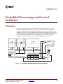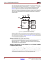
1
Spartan-3 Generation
FPGA User Guide
Spartan-3A DSP, Spartan-3AN,
Spartan-3A, Spartan-3E, and
Spartan-3 FPGA Platforms
UG331 (v1.3) February 14, 2008
R
R
Xilinx is disclosing this Document and Intellectual Property (hereinafter “the Design”) to you for use in the development of designs to operate
on, or interface with Xilinx FPGAs. Except as stated herein, none of the Design may be copied, reproduced, distributed, republished,
downloaded, displayed, posted, or transmitted in any form or by any means including, but not limited to, electronic, mechanical,
photocopying, recording, or otherwise, without the prior written consent of Xilinx. Any unauthorized use of the Design may violate copyright
laws, trademark laws, the laws of privacy and publicity, and communications regulations and statutes.
Xilinx does not assume any liability arising out of the application or use of the Design; nor does Xilinx convey any license under its patents,
copyrights, or any rights of others. You are responsible for obtaining any rights you may require for your use or implementation of the Design.
Xilinx reserves the right to make changes, at any time, to the Design as deemed desirable in the sole discretion of Xilinx. Xilinx assumes no
obligation to correct any errors contained herein or to advise you of any correction if such be made. Xilinx will not assume any liability for the
accuracy or correctness of any engineering or technical support or assistance provided to you in connection with the Design.
THE DESIGN IS PROVIDED “AS IS” WITH ALL FAULTS, AND THE ENTIRE RISK AS TO ITS FUNCTION AND IMPLEMENTATION IS
WITH YOU. YOU ACKNOWLEDGE AND AGREE THAT YOU HAVE NOT RELIED ON ANY ORAL OR WRITTEN INFORMATION OR
ADVICE, WHETHER GIVEN BY XILINX, OR ITS AGENTS OR EMPLOYEES. XILINX MAKES NO OTHER WARRANTIES, WHETHER
EXPRESS, IMPLIED, OR STATUTORY, REGARDING THE DESIGN, INCLUDING ANY WARRANTIES OF MERCHANTABILITY, FITNESS
FOR A PARTICULAR PURPOSE, TITLE, AND NONINFRINGEMENT OF THIRD-PARTY RIGHTS.
IN NO EVENT WILL XILINX BE LIABLE FOR ANY CONSEQUENTIAL, INDIRECT, EXEMPLARY, SPECIAL, OR INCIDENTAL DAMAGES,
INCLUDING ANY LOST DATA AND LOST PROFITS, ARISING FROM OR RELATING TO YOUR USE OF THE DESIGN, EVEN IF YOU
HAVE BEEN ADVISED OF THE POSSIBILITY OF SUCH DAMAGES. THE TOTAL CUMULATIVE LIABILITY OF XILINX IN CONNECTION
WITH YOUR USE OF THE DESIGN, WHETHER IN CONTRACT OR TORT OR OTHERWISE, WILL IN NO EVENT EXCEED THE
AMOUNT OF FEES PAID BY YOU TO XILINX HEREUNDER FOR USE OF THE DESIGN. YOU ACKNOWLEDGE THAT THE FEES, IF
ANY, REFLECT THE ALLOCATION OF RISK SET FORTH IN THIS AGREEMENT cc THAT XILINX WOULD NOT MAKE AVAILABLE THE
DESIGN TO YOU WITHOUT THESE LIMITATIONS OF LIABILITY.
The Design is not designed or intended for use in the development of on-line control equipment in hazardous environments requiring failsafe controls, such as in the operation of nuclear facilities, aircraft navigation or communications systems, air traffic control, life support, or
weapons systems (“High-Risk Applications”). Xilinx specifically disclaims any express or implied warranties of fitness for such High-Risk
Applications. You represent that use of the Design in such High-Risk Applications is fully at your risk.
© 2002-2007 Xilinx, Inc. All rights reserved. XILINX, the Xilinx logo, and other designated brands included herein are trademarks of Xilinx,
Inc. PowerPC is a trademark of IBM Corp. and used under license. PCI, PCI-X, and PCI EXPRESS are registered trademarks of PCI-SIG.
All other trademarks are the property of their respective owners.
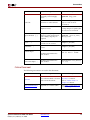
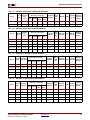
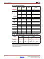
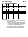
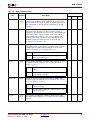
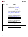
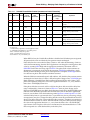
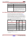
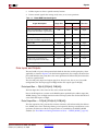
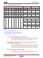
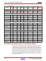
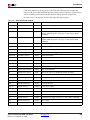
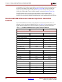
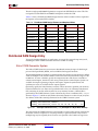
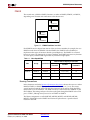
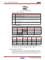
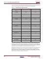
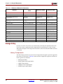
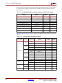
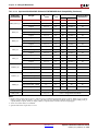
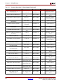
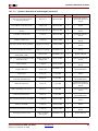
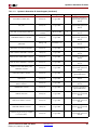
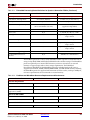
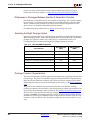
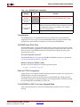
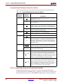
Revision History
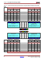
The following table shows the revision history for this document.
Date
Version
Revision
12/05/06
1.0
Initial release.
02/26/07
1.1
Added Spartan-3AN family.
04/02/07
1.2
Added Spartan-3A DSP family.
2/14/08
1.3
Updated for latest package offerings. Updated and corrected descriptions and figures
throughout. Updated links for new xilinx.com navigation.
Spartan-3 Generation FPGA User Guide
www.xilinx.com
UG331 (v1.3) February 14, 2008
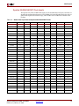
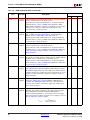
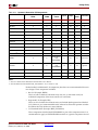
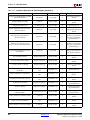
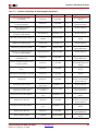
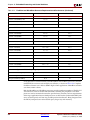
Table of Contents
Preface: About This Guide
Guide Contents . . . . . . . . . . . . . . . . . . . . . . . . . . . . . . . . . . . . . . . . . . . . . . . . . . . . . . . . . . . . . 21
Additional Resources . . . . . . . . . . . . . . . . . . . . . . . . . . . . . . . . . . . . . . . . . . . . . . . . . . . . . . . 22
Conventions . . . . . . . . . . . . . . . . . . . . . . . . . . . . . . . . . . . . . . . . . . . . . . . . . . . . . . . . . . . . . . . . 22
Typographical . . . . . . . . . . . . . . . . . . . . . . . . . . . . . . . . . . . . . . . . . . . . . . . . . . . . . . . . . . . . 22
Online Document . . . . . . . . . . . . . . . . . . . . . . . . . . . . . . . . . . . . . . . . . . . . . . . . . . . . . . . . . 23
Section I: Designing with Spartan-3 Generation FPGAs
Chapter 1: Overview
Introduction . . . . . . . . . . . . . . . . . . . . . . . . . . . . . . . . . . . . . . . . . . . . . . . . . . . . . . . . . . . . . . . . 27
Spartan-3 Generation Platforms . . . . . . . . . . . . . . . . . . . . . . . . . . . . . . . . . . . . . . . . . . . . . 28
Spartan-3 Generation Features. . . . . . . . . . . . . . . . . . . . . . . . . . . . . . . . . . . . . . . . . . . . . . . 29
Spartan-3E/3A Additional Features . . . . . . . . . . . . . . . . . . . . . . . . . . . . . . . . . . . . . . . . .
Spartan-3A Additional Features . . . . . . . . . . . . . . . . . . . . . . . . . . . . . . . . . . . . . . . . . . . .
Spartan-3AN Additional Features . . . . . . . . . . . . . . . . . . . . . . . . . . . . . . . . . . . . . . . . . . .
Spartan-3A DSP Additional Features . . . . . . . . . . . . . . . . . . . . . . . . . . . . . . . . . . . . . . . .
31
31
32
32
Spartan-3 Generation Resources . . . . . . . . . . . . . . . . . . . . . . . . . . . . . . . . . . . . . . . . . . . . .
Architectural Overview . . . . . . . . . . . . . . . . . . . . . . . . . . . . . . . . . . . . . . . . . . . . . . . . . . . . .
Configuration . . . . . . . . . . . . . . . . . . . . . . . . . . . . . . . . . . . . . . . . . . . . . . . . . . . . . . . . . . . . . . .
I/O Capabilities . . . . . . . . . . . . . . . . . . . . . . . . . . . . . . . . . . . . . . . . . . . . . . . . . . . . . . . . . . . . .
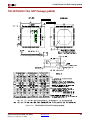
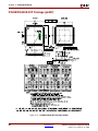
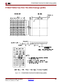
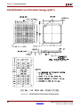
Package Marking. . . . . . . . . . . . . . . . . . . . . . . . . . . . . . . . . . . . . . . . . . . . . . . . . . . . . . . . . . . .
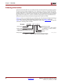
Ordering Information . . . . . . . . . . . . . . . . . . . . . . . . . . . . . . . . . . . . . . . . . . . . . . . . . . . . . . .
32
35
36
37
41
42
Chapter 2: Using Global Clock Resources
Summary . . . . . . . . . . . . . . . . . . . . . . . . . . . . . . . . . . . . . . . . . . . . . . . . . . . . . . . . . . . . . . . . . . .
Introduction . . . . . . . . . . . . . . . . . . . . . . . . . . . . . . . . . . . . . . . . . . . . . . . . . . . . . . . . . . . . . . . .
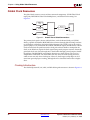
Global Clock Resource Differences between Spartan-3 Generation Families .
Global Clock Resources . . . . . . . . . . . . . . . . . . . . . . . . . . . . . . . . . . . . . . . . . . . . . . . . . . . . .
43
43
43
44
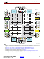
Clocking Infrastructure . . . . . . . . . . . . . . . . . . . . . . . . . . . . . . . . . . . . . . . . . . . . . . . . . . . . 44
Clock Inputs . . . . . . . . . . . . . . . . . . . . . . . . . . . . . . . . . . . . . . . . . . . . . . . . . . . . . . . . . . . . . . . . 46
Spartan-3A/3AN/3A DSP Clock Inputs . . . . . . . . . . . . . . . . . . . . . . . . . . . . . . . . . . . . .
Spartan-3E Clock Inputs . . . . . . . . . . . . . . . . . . . . . . . . . . . . . . . . . . . . . . . . . . . . . . . . . . .
Spartan-3 Clock Inputs . . . . . . . . . . . . . . . . . . . . . . . . . . . . . . . . . . . . . . . . . . . . . . . . . . . .
Clock Inputs and DCMs . . . . . . . . . . . . . . . . . . . . . . . . . . . . . . . . . . . . . . . . . . . . . . . . . . .
Differential Clocks Using Two Inputs . . . . . . . . . . . . . . . . . . . . . . . . . . . . . . . . . . . . . . .
Using Dedicated Clock Inputs in a Design . . . . . . . . . . . . . . . . . . . . . . . . . . . . . . . . . . .
IBUFG . . . . . . . . . . . . . . . . . . . . . . . . . . . . . . . . . . . . . . . . . . . . . . . . . . . . . . . . . . . . . . .
IBUFGDS . . . . . . . . . . . . . . . . . . . . . . . . . . . . . . . . . . . . . . . . . . . . . . . . . . . . . . . . . . . .
Spartan-3 Generation FPGA User Guide
UG331 (v1.3) February 14, 2008
www.xilinx.com
47
48
49
49
49
50
50
50
3
R
Clock Buffers/Multiplexers . . . . . . . . . . . . . . . . . . . . . . . . . . . . . . . . . . . . . . . . . . . . . . . . . . 51
BUFGMUX Multiplexing Details . . . . . . . . . . . . . . . . . . . . . . . . . . . . . . . . . . . . . . . . . . . .
Using Clock Buffers/Multiplexers in a Design . . . . . . . . . . . . . . . . . . . . . . . . . . . . . . . .
BUFGMUX and BUFGMUX_1 . . . . . . . . . . . . . . . . . . . . . . . . . . . . . . . . . . . . . . . . . . . .
BUFG . . . . . . . . . . . . . . . . . . . . . . . . . . . . . . . . . . . . . . . . . . . . . . . . . . . . . . . . . . . . . . .
BUFGCE and BUFGCE_1 . . . . . . . . . . . . . . . . . . . . . . . . . . . . . . . . . . . . . . . . . . . . . . . .
XST Synthesis of Clock Buffers . . . . . . . . . . . . . . . . . . . . . . . . . . . . . . . . . . . . . . . . . . . . .
52
52
52
53
53
54
BUFGMUX Connection Details. . . . . . . . . . . . . . . . . . . . . . . . . . . . . . . . . . . . . . . . . . . . . . 54
BUFGMUX Inputs . . . . . . . . . . . . . . . . . . . . . . . . . . . . . . . . . . . . . . . . . . . . . . . . . . . . . . . . 54
BUFGMUX Outputs . . . . . . . . . . . . . . . . . . . . . . . . . . . . . . . . . . . . . . . . . . . . . . . . . . . . . . 56
Spartan-3 Global Clock Buffers . . . . . . . . . . . . . . . . . . . . . . . . . . . . . . . . . . . . . . . . . . . . . 57
Quadrant Clock Routing . . . . . . . . . . . . . . . . . . . . . . . . . . . . . . . . . . . . . . . . . . . . . . . . . . . . 57
Choosing Top/Bottom and Left-/Right-Half Global Buffers . . . . . . . . . . . . . . . . . . . . 59
Spartan-3 Global Clock Routing . . . . . . . . . . . . . . . . . . . . . . . . . . . . . . . . . . . . . . . . . . . . 59
Other Information . . . . . . . . . . . . . . . . . . . . . . . . . . . . . . . . . . . . . . . . . . . . . . . . . . . . . . . . . . 59
Clock Power Consumption. . . . . . . . . . . . . . . . . . . . . . . . . . . . . . . . . . . . . . . . . . . . . . . . . 59
Clock Setup and Hold Timing . . . . . . . . . . . . . . . . . . . . . . . . . . . . . . . . . . . . . . . . . . . . . . 59
Summary . . . . . . . . . . . . . . . . . . . . . . . . . . . . . . . . . . . . . . . . . . . . . . . . . . . . . . . . . . . . . . . . . . . 60
Additional Information . . . . . . . . . . . . . . . . . . . . . . . . . . . . . . . . . . . . . . . . . . . . . . . . . . . . 60
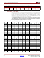
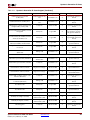
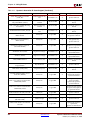
Chapter 3: Using Digital Clock Managers (DCMs)
Summary . . . . . . . . . . . . . . . . . . . . . . . . . . . . . . . . . . . . . . . . . . . . . . . . . . . . . . . . . . . . . . . . . . .
Introduction . . . . . . . . . . . . . . . . . . . . . . . . . . . . . . . . . . . . . . . . . . . . . . . . . . . . . . . . . . . . . . . .
Document Overview . . . . . . . . . . . . . . . . . . . . . . . . . . . . . . . . . . . . . . . . . . . . . . . . . . . . . . . .
Compatibility and Comparison with Other Xilinx FPGA Families . . . . . . . . . . . .
DCM Locations and Clock Distribution Network Interface . . . . . . . . . . . . . . . . . .
DCM Functional Overview . . . . . . . . . . . . . . . . . . . . . . . . . . . . . . . . . . . . . . . . . . . . . . . . . .
Delay-Locked Loop (DLL) . . . . . . . . . . . . . . . . . . . . . . . . . . . . . . . . . . . . . . . . . . . . . . . . .
Digital Frequency Synthesizer (DFS) . . . . . . . . . . . . . . . . . . . . . . . . . . . . . . . . . . . . . . . .
Phase Shift (PS) . . . . . . . . . . . . . . . . . . . . . . . . . . . . . . . . . . . . . . . . . . . . . . . . . . . . . . . . . . .
Status Logic . . . . . . . . . . . . . . . . . . . . . . . . . . . . . . . . . . . . . . . . . . . . . . . . . . . . . . . . . . . . . .
61
61
62
63
64
65
66
66
66
67
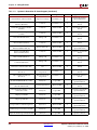
DCM Primitive. . . . . . . . . . . . . . . . . . . . . . . . . . . . . . . . . . . . . . . . . . . . . . . . . . . . . . . . . . . . . . 67
Symbol . . . . . . . . . . . . . . . . . . . . . . . . . . . . . . . . . . . . . . . . . . . . . . . . . . . . . . . . . . . . . . . . . . 68
Connection Ports . . . . . . . . . . . . . . . . . . . . . . . . . . . . . . . . . . . . . . . . . . . . . . . . . . . . . . . . . 68
Attributes, Properties, or Constraints . . . . . . . . . . . . . . . . . . . . . . . . . . . . . . . . . . . . . . . . 72
DCM Clock Requirements . . . . . . . . . . . . . . . . . . . . . . . . . . . . . . . . . . . . . . . . . . . . . . . . . . 76
Input Clock Frequency Range . . . . . . . . . . . . . . . . . . . . . . . . . . . . . . . . . . . . . . . . . . . . . .
Output Clock Frequency Range . . . . . . . . . . . . . . . . . . . . . . . . . . . . . . . . . . . . . . . . . . . . .
Input Clock and Clock Feedback Variation . . . . . . . . . . . . . . . . . . . . . . . . . . . . . . . . . . .
Cycle-to-Cycle Jitter . . . . . . . . . . . . . . . . . . . . . . . . . . . . . . . . . . . . . . . . . . . . . . . . . . . .
Period Jitter . . . . . . . . . . . . . . . . . . . . . . . . . . . . . . . . . . . . . . . . . . . . . . . . . . . . . . . . . . .
DLL Feedback Delay Variance . . . . . . . . . . . . . . . . . . . . . . . . . . . . . . . . . . . . . . . . . . . .
Optimal DCM Clock and External Feedback Inputs . . . . . . . . . . . . . . . . . . . . . . . . . . .
Spartan-3E FPGA DCM Clock Inputs . . . . . . . . . . . . . . . . . . . . . . . . . . . . . . . . . . . . . . .
Spartan-3A/3AN/3A DSP FPGA DCM Clock Inputs . . . . . . . . . . . . . . . . . . . . . . . . . .
76
77
77
78
78
79
79
79
82
LOCKED Output Behavior . . . . . . . . . . . . . . . . . . . . . . . . . . . . . . . . . . . . . . . . . . . . . . . . . . 85
RST Input Behavior . . . . . . . . . . . . . . . . . . . . . . . . . . . . . . . . . . . . . . . . . . . . . . . . . . . . . . . . . 86
Spartan-3A DCM Digital Frequency Synthesizer Requires Add’l Lock Circuitry . . . 87
4
www.xilinx.com
Spartan-3 Generation FPGA User Guide
UG331 (v1.3) February 14, 2008
R
Clocking Wizard . . . . . . . . . . . . . . . . . . . . . . . . . . . . . . . . . . . . . . . . . . . . . . . . . . . . . . . . . . . . 87
Invoking Clocking Wizard . . . . . . . . . . . . . . . . . . . . . . . . . . . . . . . . . . . . . . . . . . . . . . . . .
From Windows Start Button . . . . . . . . . . . . . . . . . . . . . . . . . . . . . . . . . . . . . . . . . . . . . .
From within Project Navigator . . . . . . . . . . . . . . . . . . . . . . . . . . . . . . . . . . . . . . . . . . . .
General Setup . . . . . . . . . . . . . . . . . . . . . . . . . . . . . . . . . . . . . . . . . . . . . . . . . . . . . . . . . . . .
Advanced Options . . . . . . . . . . . . . . . . . . . . . . . . . . . . . . . . . . . . . . . . . . . . . . . . . . . . . . . .
Clock Buffers . . . . . . . . . . . . . . . . . . . . . . . . . . . . . . . . . . . . . . . . . . . . . . . . . . . . . . . . . . . . .
Clock Frequency Synthesizer . . . . . . . . . . . . . . . . . . . . . . . . . . . . . . . . . . . . . . . . . . . . . . .
Generating HDL Output . . . . . . . . . . . . . . . . . . . . . . . . . . . . . . . . . . . . . . . . . . . . . . . . . . .
88
88
89
90
92
93
94
95
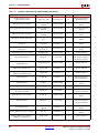
VHDL and Verilog Instantiation . . . . . . . . . . . . . . . . . . . . . . . . . . . . . . . . . . . . . . . . . . . . 96
Language Templates within Project Navigator. . . . . . . . . . . . . . . . . . . . . . . . . . . . . . . . 96
Eliminating Clock Skew. . . . . . . . . . . . . . . . . . . . . . . . . . . . . . . . . . . . . . . . . . . . . . . . . . . . . 97
What is Clock Skew? . . . . . . . . . . . . . . . . . . . . . . . . . . . . . . . . . . . . . . . . . . . . . . . . . . . . . . 97
Clock Skew: The Performance Thief . . . . . . . . . . . . . . . . . . . . . . . . . . . . . . . . . . . . . . . . . 98
Make It Go Away! . . . . . . . . . . . . . . . . . . . . . . . . . . . . . . . . . . . . . . . . . . . . . . . . . . . . . . . . 98
Predicting the Future by Closely Examining the Past . . . . . . . . . . . . . . . . . . . . . . . . . . 99
Locked on Target . . . . . . . . . . . . . . . . . . . . . . . . . . . . . . . . . . . . . . . . . . . . . . . . . . . . . . . . 100
A Stable, Monotonic Clock Input. . . . . . . . . . . . . . . . . . . . . . . . . . . . . . . . . . . . . . . . . . . 100
Feedback from a Reliable Source . . . . . . . . . . . . . . . . . . . . . . . . . . . . . . . . . . . . . . . . . . . 101
Removing Skew from an Internal Clock . . . . . . . . . . . . . . . . . . . . . . . . . . . . . . . . . . . . . 101
Removing Skew from an External Clock . . . . . . . . . . . . . . . . . . . . . . . . . . . . . . . . . . . . 102
Reset DCM After Configuration . . . . . . . . . . . . . . . . . . . . . . . . . . . . . . . . . . . . . . . . . . 102
Why Reset? . . . . . . . . . . . . . . . . . . . . . . . . . . . . . . . . . . . . . . . . . . . . . . . . . . . . . . . . . . 103
What is a Delay-Locked Loop? . . . . . . . . . . . . . . . . . . . . . . . . . . . . . . . . . . . . . . . . . . . . 104
Delay-Locked Loop (DLL) . . . . . . . . . . . . . . . . . . . . . . . . . . . . . . . . . . . . . . . . . . . . . . 104
Phase-Locked Loop (PLL) . . . . . . . . . . . . . . . . . . . . . . . . . . . . . . . . . . . . . . . . . . . . . . . 105
Implementation. . . . . . . . . . . . . . . . . . . . . . . . . . . . . . . . . . . . . . . . . . . . . . . . . . . . . . . 105
DLL vs. PLL . . . . . . . . . . . . . . . . . . . . . . . . . . . . . . . . . . . . . . . . . . . . . . . . . . . . . . . . . 105
Skew Adjustment . . . . . . . . . . . . . . . . . . . . . . . . . . . . . . . . . . . . . . . . . . . . . . . . . . . . . . . . 105
System Synchronous . . . . . . . . . . . . . . . . . . . . . . . . . . . . . . . . . . . . . . . . . . . . . . . . . . . 105
Source Synchronous . . . . . . . . . . . . . . . . . . . . . . . . . . . . . . . . . . . . . . . . . . . . . . . . . . . 106
Timing Comparisons . . . . . . . . . . . . . . . . . . . . . . . . . . . . . . . . . . . . . . . . . . . . . . . . . . 107
Clock Conditioning . . . . . . . . . . . . . . . . . . . . . . . . . . . . . . . . . . . . . . . . . . . . . . . . . . . . . . . . 107
Spartan-3E and Spartan-3A/3AN/3A DSP FPGA Output Clock Conditioning . . . 108
Spartan-3 FPGA Output Clock Conditioning . . . . . . . . . . . . . . . . . . . . . . . . . . . . . . . . 108
Phase Shifting – Delaying Clock Outputs by a Fraction of a Period . . . . . . . . . . 109
Half-Period Phase Shifted Outputs . . . . . . . . . . . . . . . . . . . . . . . . . . . . . . . . . . . . . . . . .
Half-Period Phase Shift Outputs Reduce Duty-Cycle Distortion . . . . . . . . . . . . . . . . .
Dual-Data Rate (DDR) Clocking Example . . . . . . . . . . . . . . . . . . . . . . . . . . . . . . . . . .
Quadrant Phase Shifted Outputs . . . . . . . . . . . . . . . . . . . . . . . . . . . . . . . . . . . . . . . . . . .
Output Availability Depends on DLL Frequency Mode . . . . . . . . . . . . . . . . . . . . . . . .
Spartan-3 FPGA: Optional 50/50 Duty Cycle Correction . . . . . . . . . . . . . . . . . . . . . . .
Four Phases, Delayed Clock Edges, Phased Pulses . . . . . . . . . . . . . . . . . . . . . . . . . . . .
Fine Phase Shifting . . . . . . . . . . . . . . . . . . . . . . . . . . . . . . . . . . . . . . . . . . . . . . . . . . . . . . .
Fixed Fine Phase Shifting . . . . . . . . . . . . . . . . . . . . . . . . . . . . . . . . . . . . . . . . . . . . . . . . .
Spartan-3 Family Fixed Fine Phase Shift Range . . . . . . . . . . . . . . . . . . . . . . . . . . . . . .
Minimum Phase Shift Size . . . . . . . . . . . . . . . . . . . . . . . . . . . . . . . . . . . . . . . . . . . . . .
Other Design Considerations . . . . . . . . . . . . . . . . . . . . . . . . . . . . . . . . . . . . . . . . . . . .
Clocking Wizard . . . . . . . . . . . . . . . . . . . . . . . . . . . . . . . . . . . . . . . . . . . . . . . . . . . . . .
Spartan-3 Generation FPGA User Guide
UG331 (v1.3) February 14, 2008
www.xilinx.com
110
111
111
112
113
113
114
114
115
115
117
117
117
5
R
Variable Fine Phase Shifting . . . . . . . . . . . . . . . . . . . . . . . . . . . . . . . . . . . . . . . . . . . . . . .
Important Differences Between Spartan-3 Generation FPGA Families . . . . . . . . . . . . .
Spartan-3E and Spartan-3A/3AN/3A DSP Variable Phase Shift Operations . . . . . . . .
Operation . . . . . . . . . . . . . . . . . . . . . . . . . . . . . . . . . . . . . . . . . . . . . . . . . . . . . . . . . . .
Variable Fine Phase Shift Range . . . . . . . . . . . . . . . . . . . . . . . . . . . . . . . . . . . . . . . . . .
Spartan-3 FPGA Family Variable Phase Shift Range . . . . . . . . . . . . . . . . . . . . . . . . . .
Spartan-3E and Spartan-3A/3AN/3A DSP FPGA Family Variable Phase Shift Range
Controls . . . . . . . . . . . . . . . . . . . . . . . . . . . . . . . . . . . . . . . . . . . . . . . . . . . . . . . . . . . .
Clocking Wizard . . . . . . . . . . . . . . . . . . . . . . . . . . . . . . . . . . . . . . . . . . . . . . . . . . . . . .
Example Applications . . . . . . . . . . . . . . . . . . . . . . . . . . . . . . . . . . . . . . . . . . . . . . . . . .
118
118
119
120
121
121
122
122
124
124
Clock Multiplication, Clock Division, and Frequency Synthesis . . . . . . . . . . . . 124
Frequency Synthesis Applications . . . . . . . . . . . . . . . . . . . . . . . . . . . . . . . . . . . . . . . . .
Input and Output Clock Frequency Restrictions . . . . . . . . . . . . . . . . . . . . . . . . . . . . .
Clock Doubler (CLK2X, CLK2X180) . . . . . . . . . . . . . . . . . . . . . . . . . . . . . . . . . . . . . . . .
Clock Divider (CLKDV) . . . . . . . . . . . . . . . . . . . . . . . . . . . . . . . . . . . . . . . . . . . . . . . . . .
CLKDV Clock Conditioning . . . . . . . . . . . . . . . . . . . . . . . . . . . . . . . . . . . . . . . . . . . . .
CLKDV Jitter Depends on Frequency Mode and Integer or Non-Integer Value. . . . . .
Clocking Wizard . . . . . . . . . . . . . . . . . . . . . . . . . . . . . . . . . . . . . . . . . . . . . . . . . . . . . .
Frequency Synthesizer (CLKFX, CLKFX180) . . . . . . . . . . . . . . . . . . . . . . . . . . . . . . . . .
Clocking Wizard . . . . . . . . . . . . . . . . . . . . . . . . . . . . . . . . . . . . . . . . . . . . . . . . . . . . . .
126
127
128
129
130
131
131
131
133
Clock Forwarding, Mirroring, Rebuffering . . . . . . . . . . . . . . . . . . . . . . . . . . . . . . . . . 134
Clock Jitter or Phase Noise . . . . . . . . . . . . . . . . . . . . . . . . . . . . . . . . . . . . . . . . . . . . . . . . . 135
What is Clock Jitter? . . . . . . . . . . . . . . . . . . . . . . . . . . . . . . . . . . . . . . . . . . . . . . . . . . . . .
What Causes Clock Jitter? . . . . . . . . . . . . . . . . . . . . . . . . . . . . . . . . . . . . . . . . . . . . . . . . .
Understanding Clock Jitter Specifications . . . . . . . . . . . . . . . . . . . . . . . . . . . . . . . . . . .
Cycle-to-Cycle Jitter . . . . . . . . . . . . . . . . . . . . . . . . . . . . . . . . . . . . . . . . . . . . . . . . . . .
Period Jitter . . . . . . . . . . . . . . . . . . . . . . . . . . . . . . . . . . . . . . . . . . . . . . . . . . . . . . . . . .
Unit Interval (UI) . . . . . . . . . . . . . . . . . . . . . . . . . . . . . . . . . . . . . . . . . . . . . . . . . . . . .
Calculating Total Jitter . . . . . . . . . . . . . . . . . . . . . . . . . . . . . . . . . . . . . . . . . . . . . . . . . . .
Adding Input Jitter to DLL Output Jitter . . . . . . . . . . . . . . . . . . . . . . . . . . . . . . . . . . .
Calculating Jitter for Cascaded DCMs . . . . . . . . . . . . . . . . . . . . . . . . . . . . . . . . . . . . . .
Example 1: All DCMs Use DLL Outputs . . . . . . . . . . . . . . . . . . . . . . . . . . . . . . . . . . .
Example 2: Some DCMs Use the CLKFX or CLKFX180 Outputs . . . . . . . . . . . . . . . . .
Cascaded DCM Design Recommendations . . . . . . . . . . . . . . . . . . . . . . . . . . . . . . . . .
Jitter Effect on System Performance . . . . . . . . . . . . . . . . . . . . . . . . . . . . . . . . . . . . . . . .
Example . . . . . . . . . . . . . . . . . . . . . . . . . . . . . . . . . . . . . . . . . . . . . . . . . . . . . . . . . . . .
Recommended Design Practices to Minimize Clock Jitter. . . . . . . . . . . . . . . . . . . . . .
Properly Design the Power Distribution System . . . . . . . . . . . . . . . . . . . . . . . . . . . . .
Properly Design the Printed Circuit Board . . . . . . . . . . . . . . . . . . . . . . . . . . . . . . . . . .
Obey Simultaneous Switching Output (SSO) Recommendations . . . . . . . . . . . . . . . . .
Optionally Place Virtual Ground Pins Around DCM Input and Output Connections .
VCCAUX Considerations for Improving Jitter Performance . . . . . . . . . . . . . . . . . . . . . .
Adjusting FACTORY_JF Setting (Spartan-3 FPGA Family Only) . . . . . . . . . . . . . . . . .
135
136
136
136
137
137
138
138
139
139
140
140
140
141
141
141
141
142
142
143
143
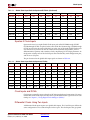
Miscellaneous Advanced Topics . . . . . . . . . . . . . . . . . . . . . . . . . . . . . . . . . . . . . . . . . . . . 144
Bitstream Generation Settings . . . . . . . . . . . . . . . . . . . . . . . . . . . . . . . . . . . . . . . . . . . . .
Setting Bitstream Generation Options in Project Navigator . . . . . . . . . . . . . . . . . . . . .
Setting Bitstream Generation Options via Command Line or Script . . . . . . . . . . . . . .
Setting Configuration Logic to Wait for DCM LOCKED Output . . . . . . . . . . . . . . . . .
144
144
144
144
Reset DCM During Partial Reconfiguration or During Full Reconfiguration via JTAG 146
Momentarily Stopping CLKIN . . . . . . . . . . . . . . . . . . . . . . . . . . . . . . . . . . . . . . . . . . . . 146
Related Materials and References . . . . . . . . . . . . . . . . . . . . . . . . . . . . . . . . . . . . . . . . . . 147
6
www.xilinx.com
Spartan-3 Generation FPGA User Guide
UG331 (v1.3) February 14, 2008
R
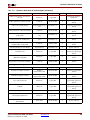
Chapter 4: Using Block RAM
Summary . . . . . . . . . . . . . . . . . . . . . . . . . . . . . . . . . . . . . . . . . . . . . . . . . . . . . . . . . . . . . . . . . .
Introduction . . . . . . . . . . . . . . . . . . . . . . . . . . . . . . . . . . . . . . . . . . . . . . . . . . . . . . . . . . . . . . .
Block RAM Differences between Spartan-3 Generation Families . . . . . . . . . . . .
Block RAM Location and Surrounding Neighborhood . . . . . . . . . . . . . . . . . . . . . .
149
149
152
153
Block RAM/Multiplier Routing Interaction . . . . . . . . . . . . . . . . . . . . . . . . . . . . . . . . . 154
Data Flows . . . . . . . . . . . . . . . . . . . . . . . . . . . . . . . . . . . . . . . . . . . . . . . . . . . . . . . . . . . . . . . . . 154
Signals . . . . . . . . . . . . . . . . . . . . . . . . . . . . . . . . . . . . . . . . . . . . . . . . . . . . . . . . . . . . . . . . . . . . . 154
Data Inputs and Outputs . . . . . . . . . . . . . . . . . . . . . . . . . . . . . . . . . . . . . . . . . . . . . . . . .
Data Input Bus — DI[#:0] (DIA[#:0], DIB[#:0]) . . . . . . . . . . . . . . . . . . . . . . . . . . . . . . .
Data Output Bus — DO[#:0] (DOA[#:0], DOB[#:0]) . . . . . . . . . . . . . . . . . . . . . . . . . . .
Parity Inputs and Outputs . . . . . . . . . . . . . . . . . . . . . . . . . . . . . . . . . . . . . . . . . . . . . . . .
Data Input Parity Bus — DIP[#:0] (DIPA[#:0], DIPB[#:0]) . . . . . . . . . . . . . . . . . . . . . . .
Data Output Parity Bus — DOP[#:0] (DOPA[#:0], DOPB[#:0]) . . . . . . . . . . . . . . . . . . .
Address Input . . . . . . . . . . . . . . . . . . . . . . . . . . . . . . . . . . . . . . . . . . . . . . . . . . . . . . . . . . .
Address Bus — ADDR[#:0] (ADDRA[#:0], ADDRB[#:0]) . . . . . . . . . . . . . . . . . . . . . . .
Control Inputs . . . . . . . . . . . . . . . . . . . . . . . . . . . . . . . . . . . . . . . . . . . . . . . . . . . . . . . . . .
Clock — CLK (CLKA, CLKB) . . . . . . . . . . . . . . . . . . . . . . . . . . . . . . . . . . . . . . . . . . . .
Enable — EN (ENA, ENB) . . . . . . . . . . . . . . . . . . . . . . . . . . . . . . . . . . . . . . . . . . . . . .
Write Enable — WE (WEA, WEB) . . . . . . . . . . . . . . . . . . . . . . . . . . . . . . . . . . . . . . . .
Output Register Enable - REGCE (REGCEA, REGCEB) Spartan-3A DSP Only . . . . . .
Output Latch Synchronous Set/Reset — SSR (SSRA, SSRB) . . . . . . . . . . . . . . . . . . . .
Output Latch/Register Sync/Async Set/Reset - RST - Spartan-3A DSP Only . . . . . . .
Global Set/Reset — GSR . . . . . . . . . . . . . . . . . . . . . . . . . . . . . . . . . . . . . . . . . . . . . . . .
Inverting Control Pins . . . . . . . . . . . . . . . . . . . . . . . . . . . . . . . . . . . . . . . . . . . . . . . . .
Unused Inputs . . . . . . . . . . . . . . . . . . . . . . . . . . . . . . . . . . . . . . . . . . . . . . . . . . . . . . .
155
155
155
156
156
156
158
158
158
158
158
158
160
160
160
161
161
161
Attributes . . . . . . . . . . . . . . . . . . . . . . . . . . . . . . . . . . . . . . . . . . . . . . . . . . . . . . . . . . . . . . . . . . 161
Number of Ports . . . . . . . . . . . . . . . . . . . . . . . . . . . . . . . . . . . . . . . . . . . . . . . . . . . . . . . . .
CORE Generator System . . . . . . . . . . . . . . . . . . . . . . . . . . . . . . . . . . . . . . . . . . . . . . . .
VHDL or Verilog Instantiation . . . . . . . . . . . . . . . . . . . . . . . . . . . . . . . . . . . . . . . . . . .
Memory Organization/Aspect Ratio . . . . . . . . . . . . . . . . . . . . . . . . . . . . . . . . . . . . . . .
CORE Generator System — Memory Size . . . . . . . . . . . . . . . . . . . . . . . . . . . . . . . . . .
VHDL or Verilog Instantiation . . . . . . . . . . . . . . . . . . . . . . . . . . . . . . . . . . . . . . . . . . .
Address and Data Mapping Between Two Ports . . . . . . . . . . . . . . . . . . . . . . . . . . . . .
Content Initialization . . . . . . . . . . . . . . . . . . . . . . . . . . . . . . . . . . . . . . . . . . . . . . . . . . . . .
CORE Generator System — Load Init File . . . . . . . . . . . . . . . . . . . . . . . . . . . . . . . . . .
VHDL or Verilog Instantiation — INIT_xx, INITP_xx . . . . . . . . . . . . . . . . . . . . . . . . .
Data Output Latch Initialization . . . . . . . . . . . . . . . . . . . . . . . . . . . . . . . . . . . . . . . . . . .
CORE Generator System — Global Init Value . . . . . . . . . . . . . . . . . . . . . . . . . . . . . . .
VHDL or Verilog Instantiation — INIT (INIT_A and INIT_B) . . . . . . . . . . . . . . . . . . .
Data Output Latch Synchronous Set/Reset Value . . . . . . . . . . . . . . . . . . . . . . . . . . . .
CORE Generator System — Init Value (SINIT) . . . . . . . . . . . . . . . . . . . . . . . . . . . . . . .
VHDL or Verilog Instantiation — SRVAL (SRVAL_A and SRVAL_B). . . . . . . . . . . . .
Read Behavior During Simultaneous Write — WRITE_MODE . . . . . . . . . . . . . . . . .
WRITE_FIRST or Transparent Mode (Default) . . . . . . . . . . . . . . . . . . . . . . . . . . . . . . .
READ_FIRST or Read-Before-Write Mode . . . . . . . . . . . . . . . . . . . . . . . . . . . . . . . . . .
NO_CHANGE Mode . . . . . . . . . . . . . . . . . . . . . . . . . . . . . . . . . . . . . . . . . . . . . . . . . .
CORE Generator System — Write Mode . . . . . . . . . . . . . . . . . . . . . . . . . . . . . . . . . . .
VHDL or Verilog Instantiation — WRITE_MODE . . . . . . . . . . . . . . . . . . . . . . . . . . . .
Location Constraints (LOC) . . . . . . . . . . . . . . . . . . . . . . . . . . . . . . . . . . . . . . . . . . . . . . .
Spartan-3 Generation FPGA User Guide
UG331 (v1.3) February 14, 2008
www.xilinx.com
162
162
162
163
163
163
164
164
165
165
166
166
166
167
167
167
167
168
169
170
171
171
171
7
R
Block RAM Operation . . . . . . . . . . . . . . . . . . . . . . . . . . . . . . . . . . . . . . . . . . . . . . . . . . . . . 172
RAM Contents Initialized During Configuration . . . . . . . . . . . . . . . . . . . . . . . . . . . . .
Global Set/Reset Initializes Data Output Latches . . . . . . . . . . . . . . . . . . . . . . . . . . . .
Enable Input Activates or Disables RAM . . . . . . . . . . . . . . . . . . . . . . . . . . . . . . . . . . . .
Synchronous Set/Reset Initializes Data Output Latches . . . . . . . . . . . . . . . . . . . . . . .
Simultaneous Write and Synchronous Set/Reset Operations . . . . . . . . . . . . . . . . . .
Read Operations Occur on Every Clock Edge When Enable is Asserted . . . . . . . . .
Write Operations Always Have Simultaneous Read Operation. . . . . . . . . . . . . . . . .
General Characteristics . . . . . . . . . . . . . . . . . . . . . . . . . . . . . . . . . . . . . . . . . . . . . . . . . . .
Functional Compatibility with Other Xilinx FPGA Families . . . . . . . . . . . . . . . . . . .
173
173
173
174
174
174
174
174
175
Dual-Port RAM Conflicts and Resolution. . . . . . . . . . . . . . . . . . . . . . . . . . . . . . . . . . . 175
Timing Violation Conflicts . . . . . . . . . . . . . . . . . . . . . . . . . . . . . . . . . . . . . . . . . . . . . . . .
Simultaneous Writes to Both Ports with Different Data Conflicts . . . . . . . . . . . . . . .
Write Mode Conflicts on Output Latches. . . . . . . . . . . . . . . . . . . . . . . . . . . . . . . . . . . .
Conflict Resolution . . . . . . . . . . . . . . . . . . . . . . . . . . . . . . . . . . . . . . . . . . . . . . . . . . . . . .
175
176
177
177
Block RAM Design Entry. . . . . . . . . . . . . . . . . . . . . . . . . . . . . . . . . . . . . . . . . . . . . . . . . . . 177
Xilinx CORE Generator System . . . . . . . . . . . . . . . . . . . . . . . . . . . . . . . . . . . . . . . . . . . .
VHDL and Verilog Instantiation . . . . . . . . . . . . . . . . . . . . . . . . . . . . . . . . . . . . . . . . . . .
Inferring Block RAM . . . . . . . . . . . . . . . . . . . . . . . . . . . . . . . . . . . . . . . . . . . . . . . . . . .
Instantiation Templates . . . . . . . . . . . . . . . . . . . . . . . . . . . . . . . . . . . . . . . . . . . . . . . .
Initialization in VHDL or Verilog Codes . . . . . . . . . . . . . . . . . . . . . . . . . . . . . . . . . . .
177
178
178
178
179
Block RAM Applications . . . . . . . . . . . . . . . . . . . . . . . . . . . . . . . . . . . . . . . . . . . . . . . . . . . 179
Creating Larger RAM Structures . . . . . . . . . . . . . . . . . . . . . . . . . . . . . . . . . . . . . . . . . . .
Block RAM as Read-Only Memory (ROM) . . . . . . . . . . . . . . . . . . . . . . . . . . . . . . . . . .
FIFOs . . . . . . . . . . . . . . . . . . . . . . . . . . . . . . . . . . . . . . . . . . . . . . . . . . . . . . . . . . . . . . . . . .
Storage for Embedded Processors . . . . . . . . . . . . . . . . . . . . . . . . . . . . . . . . . . . . . . . . . .
Updating Block RAM/ROM Content by Directly Modifying Device Bitstream . . .
Two Independent Single-Port RAMs Using One Block RAM . . . . . . . . . . . . . . . . . . .
A 256x72 Single-Port RAM Using One Block RAM . . . . . . . . . . . . . . . . . . . . . . . . . . .
Circular Buffers, Shift Registers, and Delay Lines . . . . . . . . . . . . . . . . . . . . . . . . . . . .
Fast Complex State Machines and Microsequencers . . . . . . . . . . . . . . . . . . . . . . . . . .
Fast, Long Counters Using RAM . . . . . . . . . . . . . . . . . . . . . . . . . . . . . . . . . . . . . . . . . . .
Four-Port Memory . . . . . . . . . . . . . . . . . . . . . . . . . . . . . . . . . . . . . . . . . . . . . . . . . . . . . . .
Content-Addressable Memory (CAM) . . . . . . . . . . . . . . . . . . . . . . . . . . . . . . . . . . . . . .
Implementing Logic Functions Using Block RAM . . . . . . . . . . . . . . . . . . . . . . . . . . . .
Fuzzy Pattern Matching Circuit Example . . . . . . . . . . . . . . . . . . . . . . . . . . . . . . . . . . .
Mapping Logic into Block RAM Using MAP –bp Option . . . . . . . . . . . . . . . . . . . . . . .
Waveform Storage, Function Tables, Direct Digital Synthesis Using Block RAM . .
179
179
179
180
180
181
182
183
185
186
188
188
188
189
189
190
Related Materials and References . . . . . . . . . . . . . . . . . . . . . . . . . . . . . . . . . . . . . . . . . .
Conclusion . . . . . . . . . . . . . . . . . . . . . . . . . . . . . . . . . . . . . . . . . . . . . . . . . . . . . . . . . . . . . . . . .
Appendix A: VHDL Instantiation Example . . . . . . . . . . . . . . . . . . . . . . . . . . . . . . . . .
Appendix B: Verilog Instantiation Example . . . . . . . . . . . . . . . . . . . . . . . . . . . . . . . . .
191
192
192
195
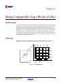
Chapter 5: Using Configurable Logic Blocks (CLBs)
CLB Overview . . . . . . . . . . . . . . . . . . . . . . . . . . . . . . . . . . . . . . . . . . . . . . . . . . . . . . . . . . . . .
CLB Array . . . . . . . . . . . . . . . . . . . . . . . . . . . . . . . . . . . . . . . . . . . . . . . . . . . . . . . . . . . . . . . . .
CLB Differences between Spartan-3 Generation Families . . . . . . . . . . . . . . . . . . .
Slices . . . . . . . . . . . . . . . . . . . . . . . . . . . . . . . . . . . . . . . . . . . . . . . . . . . . . . . . . . . . . . . . . . . . . .
197
197
198
199
Slice Location Designations . . . . . . . . . . . . . . . . . . . . . . . . . . . . . . . . . . . . . . . . . . . . . . . 201
Slice Overview . . . . . . . . . . . . . . . . . . . . . . . . . . . . . . . . . . . . . . . . . . . . . . . . . . . . . . . . . . . . . 201
8
www.xilinx.com
Spartan-3 Generation FPGA User Guide
UG331 (v1.3) February 14, 2008
R
Logic Cells . . . . . . . . . . . . . . . . . . . . . . . . . . . . . . . . . . . . . . . . . . . . . . . . . . . . . . . . . . . . . . . . .
Slice Details . . . . . . . . . . . . . . . . . . . . . . . . . . . . . . . . . . . . . . . . . . . . . . . . . . . . . . . . . . . . . . .
Main Logic Paths . . . . . . . . . . . . . . . . . . . . . . . . . . . . . . . . . . . . . . . . . . . . . . . . . . . . . . . . . . .
Look-Up Tables . . . . . . . . . . . . . . . . . . . . . . . . . . . . . . . . . . . . . . . . . . . . . . . . . . . . . . . . . . . .
Wide Multiplexers . . . . . . . . . . . . . . . . . . . . . . . . . . . . . . . . . . . . . . . . . . . . . . . . . . . . . . . . .
Carry and Arithmetic Logic . . . . . . . . . . . . . . . . . . . . . . . . . . . . . . . . . . . . . . . . . . . . . . . . .
Storage Elements . . . . . . . . . . . . . . . . . . . . . . . . . . . . . . . . . . . . . . . . . . . . . . . . . . . . . . . . . . .
202
202
204
204
205
205
205
Initialization . . . . . . . . . . . . . . . . . . . . . . . . . . . . . . . . . . . . . . . . . . . . . . . . . . . . . . . . . . . . 207
Distributed RAM . . . . . . . . . . . . . . . . . . . . . . . . . . . . . . . . . . . . . . . . . . . . . . . . . . . . . . . . . . 207
Shift Registers . . . . . . . . . . . . . . . . . . . . . . . . . . . . . . . . . . . . . . . . . . . . . . . . . . . . . . . . . . . . . 207
Chapter 6: Using Look-Up Tables as Distributed RAM
Summary . . . . . . . . . . . . . . . . . . . . . . . . . . . . . . . . . . . . . . . . . . . . . . . . . . . . . . . . . . . . . . . . . . 209
Introduction . . . . . . . . . . . . . . . . . . . . . . . . . . . . . . . . . . . . . . . . . . . . . . . . . . . . . . . . . . . . . . . 209
Single-Port and Dual-Port RAMs . . . . . . . . . . . . . . . . . . . . . . . . . . . . . . . . . . . . . . . . . .
Data Flow . . . . . . . . . . . . . . . . . . . . . . . . . . . . . . . . . . . . . . . . . . . . . . . . . . . . . . . . . . .
Write Operations . . . . . . . . . . . . . . . . . . . . . . . . . . . . . . . . . . . . . . . . . . . . . . . . . . . . . . . .
Read Operation . . . . . . . . . . . . . . . . . . . . . . . . . . . . . . . . . . . . . . . . . . . . . . . . . . . . . . . . .
Read During Write . . . . . . . . . . . . . . . . . . . . . . . . . . . . . . . . . . . . . . . . . . . . . . . . . . . . . . .
209
209
210
210
210
Characteristics . . . . . . . . . . . . . . . . . . . . . . . . . . . . . . . . . . . . . . . . . . . . . . . . . . . . . . . . . . . . .
Distributed RAM in the CLB . . . . . . . . . . . . . . . . . . . . . . . . . . . . . . . . . . . . . . . . . . . . . . .
Distributed RAM Differences between Spartan-3 Generation Families . . . . . .
Compatibility with Other Xilinx FPGA Families . . . . . . . . . . . . . . . . . . . . . . . . . . . .
Library Primitives . . . . . . . . . . . . . . . . . . . . . . . . . . . . . . . . . . . . . . . . . . . . . . . . . . . . . . . . . .
Signal Ports . . . . . . . . . . . . . . . . . . . . . . . . . . . . . . . . . . . . . . . . . . . . . . . . . . . . . . . . . . . . . . . .
211
Clock — WCLK . . . . . . . . . . . . . . . . . . . . . . . . . . . . . . . . . . . . . . . . . . . . . . . . . . . . . . . . .
Enable — WE . . . . . . . . . . . . . . . . . . . . . . . . . . . . . . . . . . . . . . . . . . . . . . . . . . . . . . . . . . .
Address — A0, A1, A2, A3 (A4, A5, A6, A7) . . . . . . . . . . . . . . . . . . . . . . . . . . . . . . . . .
Dual-Port Read Address — DPRA0, DPRA1, DPRA2, DPRA3 . . . . . . . . . . . . . . . . .
Data In — D . . . . . . . . . . . . . . . . . . . . . . . . . . . . . . . . . . . . . . . . . . . . . . . . . . . . . . . . . . . .
Data Out — O, SPO, and DPO . . . . . . . . . . . . . . . . . . . . . . . . . . . . . . . . . . . . . . . . . . . . .
Inverting Control Pins . . . . . . . . . . . . . . . . . . . . . . . . . . . . . . . . . . . . . . . . . . . . . . . . . . . .
Global Set/Reset — GSR . . . . . . . . . . . . . . . . . . . . . . . . . . . . . . . . . . . . . . . . . . . . . . . . . .
Global Write Enable — GWE . . . . . . . . . . . . . . . . . . . . . . . . . . . . . . . . . . . . . . . . . . . . . .
211
212
213
214
215
215
215
215
215
215
215
216
216
216
Attributes . . . . . . . . . . . . . . . . . . . . . . . . . . . . . . . . . . . . . . . . . . . . . . . . . . . . . . . . . . . . . . . . . . 216
Content Initialization — INIT . . . . . . . . . . . . . . . . . . . . . . . . . . . . . . . . . . . . . . . . . . . . . 216
Placement Location — LOC . . . . . . . . . . . . . . . . . . . . . . . . . . . . . . . . . . . . . . . . . . . . . . . 217
Distributed RAM Design Entry. . . . . . . . . . . . . . . . . . . . . . . . . . . . . . . . . . . . . . . . . . . . . 219
Xilinx CORE Generator System . . . . . . . . . . . . . . . . . . . . . . . . . . . . . . . . . . . . . . . . . . . .
VHDL and Verilog . . . . . . . . . . . . . . . . . . . . . . . . . . . . . . . . . . . . . . . . . . . . . . . . . . . . . . .
Inferring Distributed RAM . . . . . . . . . . . . . . . . . . . . . . . . . . . . . . . . . . . . . . . . . . . . . .
Instantiation Templates . . . . . . . . . . . . . . . . . . . . . . . . . . . . . . . . . . . . . . . . . . . . . . . .
Verilog Instantiation Template Example . . . . . . . . . . . . . . . . . . . . . . . . . . . . . . . . . . .
Wider Distributed RAM Modules. . . . . . . . . . . . . . . . . . . . . . . . . . . . . . . . . . . . . . . . .
Initialization in VHDL or Verilog Codes . . . . . . . . . . . . . . . . . . . . . . . . . . . . . . . . . . .
219
220
220
221
222
223
223
Conclusion . . . . . . . . . . . . . . . . . . . . . . . . . . . . . . . . . . . . . . . . . . . . . . . . . . . . . . . . . . . . . . . . . 223
Related Materials and References . . . . . . . . . . . . . . . . . . . . . . . . . . . . . . . . . . . . . . . . . . 223
Spartan-3 Generation FPGA User Guide
UG331 (v1.3) February 14, 2008
www.xilinx.com
9
R
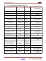
Chapter 7: Using Look-Up Tables as Shift Registers (SRL16)
Summary . . . . . . . . . . . . . . . . . . . . . . . . . . . . . . . . . . . . . . . . . . . . . . . . . . . . . . . . . . . . . . . . . .
Shift Register Differences between Spartan-3 Generation Families . . . . . . . . . .
Introduction . . . . . . . . . . . . . . . . . . . . . . . . . . . . . . . . . . . . . . . . . . . . . . . . . . . . . . . . . . . . . . .
Shift Register Architecture . . . . . . . . . . . . . . . . . . . . . . . . . . . . . . . . . . . . . . . . . . . . . . . . .
LUT Structure . . . . . . . . . . . . . . . . . . . . . . . . . . . . . . . . . . . . . . . . . . . . . . . . . . . . . . . . . . .
Dynamic Length Adjustment . . . . . . . . . . . . . . . . . . . . . . . . . . . . . . . . . . . . . . . . . . . .
Logic Cell Structure . . . . . . . . . . . . . . . . . . . . . . . . . . . . . . . . . . . . . . . . . . . . . . . . . . . . . .
Registered Output. . . . . . . . . . . . . . . . . . . . . . . . . . . . . . . . . . . . . . . . . . . . . . . . . . . . .
Slice Structure . . . . . . . . . . . . . . . . . . . . . . . . . . . . . . . . . . . . . . . . . . . . . . . . . . . . . . . . . . .
CLB Structure . . . . . . . . . . . . . . . . . . . . . . . . . . . . . . . . . . . . . . . . . . . . . . . . . . . . . . . . . . .
225
225
225
226
226
226
226
227
227
228
Library Primitives . . . . . . . . . . . . . . . . . . . . . . . . . . . . . . . . . . . . . . . . . . . . . . . . . . . . . . . . . . 230
Initialization in VHDL and Verilog Code . . . . . . . . . . . . . . . . . . . . . . . . . . . . . . . . . . .
Port Signals . . . . . . . . . . . . . . . . . . . . . . . . . . . . . . . . . . . . . . . . . . . . . . . . . . . . . . . . . . . . .
Clock — CLK . . . . . . . . . . . . . . . . . . . . . . . . . . . . . . . . . . . . . . . . . . . . . . . . . . . . . . . .
Data In — D . . . . . . . . . . . . . . . . . . . . . . . . . . . . . . . . . . . . . . . . . . . . . . . . . . . . . . . . .
Clock Enable — CE (optional) . . . . . . . . . . . . . . . . . . . . . . . . . . . . . . . . . . . . . . . . . . .
Address — A3, A2, A1, A0 . . . . . . . . . . . . . . . . . . . . . . . . . . . . . . . . . . . . . . . . . . . . . .
Data Out — Q . . . . . . . . . . . . . . . . . . . . . . . . . . . . . . . . . . . . . . . . . . . . . . . . . . . . . . . .
Data Out — Q15 (optional) . . . . . . . . . . . . . . . . . . . . . . . . . . . . . . . . . . . . . . . . . . . . . .
Inverting Control Pins . . . . . . . . . . . . . . . . . . . . . . . . . . . . . . . . . . . . . . . . . . . . . . . . .
GSR . . . . . . . . . . . . . . . . . . . . . . . . . . . . . . . . . . . . . . . . . . . . . . . . . . . . . . . . . . . . . . . .
Attributes. . . . . . . . . . . . . . . . . . . . . . . . . . . . . . . . . . . . . . . . . . . . . . . . . . . . . . . . . . . . . . .
Content Initialization — INIT . . . . . . . . . . . . . . . . . . . . . . . . . . . . . . . . . . . . . . . . . . . .
Location Constraints . . . . . . . . . . . . . . . . . . . . . . . . . . . . . . . . . . . . . . . . . . . . . . . . . . . . .
Shift Register Operations . . . . . . . . . . . . . . . . . . . . . . . . . . . . . . . . . . . . . . . . . . . . . . . . .
Data Flow . . . . . . . . . . . . . . . . . . . . . . . . . . . . . . . . . . . . . . . . . . . . . . . . . . . . . . . . . . .
Shift Operation . . . . . . . . . . . . . . . . . . . . . . . . . . . . . . . . . . . . . . . . . . . . . . . . . . . . . . .
Dynamic Read Operation . . . . . . . . . . . . . . . . . . . . . . . . . . . . . . . . . . . . . . . . . . . . . . .
Static Read Operation . . . . . . . . . . . . . . . . . . . . . . . . . . . . . . . . . . . . . . . . . . . . . . . . . .
Characteristics . . . . . . . . . . . . . . . . . . . . . . . . . . . . . . . . . . . . . . . . . . . . . . . . . . . . . . . . . .
231
231
231
231
231
231
232
232
232
232
232
232
232
233
233
234
234
235
235
Shift Register Inference . . . . . . . . . . . . . . . . . . . . . . . . . . . . . . . . . . . . . . . . . . . . . . . . . . . . 235
VHDL Inference Code . . . . . . . . . . . . . . . . . . . . . . . . . . . . . . . . . . . . . . . . . . . . . . . . . . . . 236
Verilog Inference Code . . . . . . . . . . . . . . . . . . . . . . . . . . . . . . . . . . . . . . . . . . . . . . . . . . . 236
Shift Register Submodules . . . . . . . . . . . . . . . . . . . . . . . . . . . . . . . . . . . . . . . . . . . . . . . . . 237
Fully Synchronous Shift Registers . . . . . . . . . . . . . . . . . . . . . . . . . . . . . . . . . . . . . . . . . .
Static-Length Shift Registers . . . . . . . . . . . . . . . . . . . . . . . . . . . . . . . . . . . . . . . . . . . . . . .
VHDL and Verilog Instantiation . . . . . . . . . . . . . . . . . . . . . . . . . . . . . . . . . . . . . . . . . . .
VHDL and Verilog Templates . . . . . . . . . . . . . . . . . . . . . . . . . . . . . . . . . . . . . . . . . . .
CORE Generator System . . . . . . . . . . . . . . . . . . . . . . . . . . . . . . . . . . . . . . . . . . . . . . . . . .
238
238
239
239
241
Applications . . . . . . . . . . . . . . . . . . . . . . . . . . . . . . . . . . . . . . . . . . . . . . . . . . . . . . . . . . . . . . . 242
Delay Lines . . . . . . . . . . . . . . . . . . . . . . . . . . . . . . . . . . . . . . . . . . . . . . . . . . . . . . . . . . . . .
Linear Feedback Shift Registers . . . . . . . . . . . . . . . . . . . . . . . . . . . . . . . . . . . . . . . . . . . .
Gold Code Generator . . . . . . . . . . . . . . . . . . . . . . . . . . . . . . . . . . . . . . . . . . . . . . . . . . . .
FIFOs . . . . . . . . . . . . . . . . . . . . . . . . . . . . . . . . . . . . . . . . . . . . . . . . . . . . . . . . . . . . . . . . . .
Counters . . . . . . . . . . . . . . . . . . . . . . . . . . . . . . . . . . . . . . . . . . . . . . . . . . . . . . . . . . . . . . .
242
242
243
244
244
Related Materials and References . . . . . . . . . . . . . . . . . . . . . . . . . . . . . . . . . . . . . . . . . . 245
Conclusion . . . . . . . . . . . . . . . . . . . . . . . . . . . . . . . . . . . . . . . . . . . . . . . . . . . . . . . . . . . . . . . . . 245
10
www.xilinx.com
Spartan-3 Generation FPGA User Guide
UG331 (v1.3) February 14, 2008
R
Chapter 8: Using Dedicated Multiplexers
Summary . . . . . . . . . . . . . . . . . . . . . . . . . . . . . . . . . . . . . . . . . . . . . . . . . . . . . . . . . . . . . . . . . . 247
Introduction . . . . . . . . . . . . . . . . . . . . . . . . . . . . . . . . . . . . . . . . . . . . . . . . . . . . . . . . . . . . . . . 247
Dedicated Multiplexer Differences between Spartan-3 Generation Families . 247
Advantages of Dedicated Multiplexers . . . . . . . . . . . . . . . . . . . . . . . . . . . . . . . . . . . . . 248
CLB Multiplexer Resources . . . . . . . . . . . . . . . . . . . . . . . . . . . . . . . . . . . . . . . . . . . . . . . . 249
F5MUX . . . . . . . . . . . . . . . . . . . . . . . . . . . . . . . . . . . . . . . . . . . . . . . . . . . . . . . . . . . . . . . . .
FiMUX . . . . . . . . . . . . . . . . . . . . . . . . . . . . . . . . . . . . . . . . . . . . . . . . . . . . . . . . . . . . . . . . .
Naming Conventions . . . . . . . . . . . . . . . . . . . . . . . . . . . . . . . . . . . . . . . . . . . . . . . . . .
Dedicated Local Routing . . . . . . . . . . . . . . . . . . . . . . . . . . . . . . . . . . . . . . . . . . . . . . . . . .
Mux Select Inputs . . . . . . . . . . . . . . . . . . . . . . . . . . . . . . . . . . . . . . . . . . . . . . . . . . . . . . . .
249
251
251
252
253
Implementation Examples . . . . . . . . . . . . . . . . . . . . . . . . . . . . . . . . . . . . . . . . . . . . . . . . . . 253
Wide-Input Multiplexers . . . . . . . . . . . . . . . . . . . . . . . . . . . . . . . . . . . . . . . . . . . . . . . . . 253
Wide-Input Functions . . . . . . . . . . . . . . . . . . . . . . . . . . . . . . . . . . . . . . . . . . . . . . . . . . . . 255
Timing Parameters . . . . . . . . . . . . . . . . . . . . . . . . . . . . . . . . . . . . . . . . . . . . . . . . . . . . . . . . . 258
Programmable Polarity . . . . . . . . . . . . . . . . . . . . . . . . . . . . . . . . . . . . . . . . . . . . . . . . . . . 258
Floorplanning Multiplexers . . . . . . . . . . . . . . . . . . . . . . . . . . . . . . . . . . . . . . . . . . . . . . . 258
Related Uses of Multiplexers . . . . . . . . . . . . . . . . . . . . . . . . . . . . . . . . . . . . . . . . . . . . . . . 259
Multiplexers and Three-State Buffers . . . . . . . . . . . . . . . . . . . . . . . . . . . . . . . . . . . . . . . 259
Using Memory in Place of Multiplexers . . . . . . . . . . . . . . . . . . . . . . . . . . . . . . . . . . . . . 259
Other Multiplexers . . . . . . . . . . . . . . . . . . . . . . . . . . . . . . . . . . . . . . . . . . . . . . . . . . . . . . . 259
Designing with Multiplexers . . . . . . . . . . . . . . . . . . . . . . . . . . . . . . . . . . . . . . . . . . . . . . . 260
Inference . . . . . . . . . . . . . . . . . . . . . . . . . . . . . . . . . . . . . . . . . . . . . . . . . . . . . . . . . . . . . . .
Verilog Inference. . . . . . . . . . . . . . . . . . . . . . . . . . . . . . . . . . . . . . . . . . . . . . . . . . . . . .
VHDL Inference . . . . . . . . . . . . . . . . . . . . . . . . . . . . . . . . . . . . . . . . . . . . . . . . . . . . . .
Library Primitives . . . . . . . . . . . . . . . . . . . . . . . . . . . . . . . . . . . . . . . . . . . . . . . . . . . . . . .
Enable Signals in Multiplexers . . . . . . . . . . . . . . . . . . . . . . . . . . . . . . . . . . . . . . . . . . .
Modeling Local Output Timing . . . . . . . . . . . . . . . . . . . . . . . . . . . . . . . . . . . . . . . . . .
Submodules . . . . . . . . . . . . . . . . . . . . . . . . . . . . . . . . . . . . . . . . . . . . . . . . . . . . . . . . . . . .
Port Signals . . . . . . . . . . . . . . . . . . . . . . . . . . . . . . . . . . . . . . . . . . . . . . . . . . . . . . . . . . . . .
Data In — DATA_I . . . . . . . . . . . . . . . . . . . . . . . . . . . . . . . . . . . . . . . . . . . . . . . . . . . .
Control In — SELECT_I . . . . . . . . . . . . . . . . . . . . . . . . . . . . . . . . . . . . . . . . . . . . . . . .
Data Out — DATA_O . . . . . . . . . . . . . . . . . . . . . . . . . . . . . . . . . . . . . . . . . . . . . . . . . .
Applications . . . . . . . . . . . . . . . . . . . . . . . . . . . . . . . . . . . . . . . . . . . . . . . . . . . . . . . . . . . .
VHDL and Verilog Instantiation . . . . . . . . . . . . . . . . . . . . . . . . . . . . . . . . . . . . . . . . . . .
VHDL and Verilog Submodules . . . . . . . . . . . . . . . . . . . . . . . . . . . . . . . . . . . . . . . . . .
CORE Generator System . . . . . . . . . . . . . . . . . . . . . . . . . . . . . . . . . . . . . . . . . . . . . . . . . .
260
261
261
261
262
263
263
264
264
264
264
264
264
265
268
Summary . . . . . . . . . . . . . . . . . . . . . . . . . . . . . . . . . . . . . . . . . . . . . . . . . . . . . . . . . . . . . . . . . . 269
Spartan-3 Generation FPGA User Guide
UG331 (v1.3) February 14, 2008
www.xilinx.com
11
R
Chapter 9: Using Carry and Arithmetic Logic
Summary . . . . . . . . . . . . . . . . . . . . . . . . . . . . . . . . . . . . . . . . . . . . . . . . . . . . . . . . . . . . . . . . . .
Introduction . . . . . . . . . . . . . . . . . . . . . . . . . . . . . . . . . . . . . . . . . . . . . . . . . . . . . . . . . . . . . . .
Carry and Arithmetic Logic Differences between Spartan-3 Families . . . . . . . .
Look-Ahead Carry Addition . . . . . . . . . . . . . . . . . . . . . . . . . . . . . . . . . . . . . . . . . . . . . . . .
Resource Details . . . . . . . . . . . . . . . . . . . . . . . . . . . . . . . . . . . . . . . . . . . . . . . . . . . . . . . . . . .
MUXCY . . . . . . . . . . . . . . . . . . . . . . . . . . . . . . . . . . . . . . . . . . . . . . . . . . . . . . . . . . . . . . . .
Carry Chain Bypass and Initialization . . . . . . . . . . . . . . . . . . . . . . . . . . . . . . . . . . . . . .
XORCY. . . . . . . . . . . . . . . . . . . . . . . . . . . . . . . . . . . . . . . . . . . . . . . . . . . . . . . . . . . . . . . . .
Carry Logic Connections . . . . . . . . . . . . . . . . . . . . . . . . . . . . . . . . . . . . . . . . . . . . . . . . .
Connections within a Slice . . . . . . . . . . . . . . . . . . . . . . . . . . . . . . . . . . . . . . . . . . . . . . . .
Connections between Slices and CLBs . . . . . . . . . . . . . . . . . . . . . . . . . . . . . . . . . . . . . .
Multiplication Resources . . . . . . . . . . . . . . . . . . . . . . . . . . . . . . . . . . . . . . . . . . . . . . . . . . .
Component and Pin Names . . . . . . . . . . . . . . . . . . . . . . . . . . . . . . . . . . . . . . . . . . . . . . . .
Performance . . . . . . . . . . . . . . . . . . . . . . . . . . . . . . . . . . . . . . . . . . . . . . . . . . . . . . . . . . . . . . .
Specifications . . . . . . . . . . . . . . . . . . . . . . . . . . . . . . . . . . . . . . . . . . . . . . . . . . . . . . . . . . . . . .
Designing with the Carry and Arithmetic Logic . . . . . . . . . . . . . . . . . . . . . . . . . . . . .
Library Elements Using Carry . . . . . . . . . . . . . . . . . . . . . . . . . . . . . . . . . . . . . . . . . . . . .
Primitives . . . . . . . . . . . . . . . . . . . . . . . . . . . . . . . . . . . . . . . . . . . . . . . . . . . . . . . . . . .
XORCY . . . . . . . . . . . . . . . . . . . . . . . . . . . . . . . . . . . . . . . . . . . . . . . . . . . . . . . . . . . . .
MULT_AND . . . . . . . . . . . . . . . . . . . . . . . . . . . . . . . . . . . . . . . . . . . . . . . . . . . . . . . . .
Emulating Virtex-II ORCY Components . . . . . . . . . . . . . . . . . . . . . . . . . . . . . . . . . . . .
Macros . . . . . . . . . . . . . . . . . . . . . . . . . . . . . . . . . . . . . . . . . . . . . . . . . . . . . . . . . . . . .
271
271
271
272
273
275
275
275
275
275
276
279
280
282
286
288
288
289
290
291
292
292
Using the CORE Generator System . . . . . . . . . . . . . . . . . . . . . . . . . . . . . . . . . . . . . . . . . 293
Adder . . . . . . . . . . . . . . . . . . . . . . . . . . . . . . . . . . . . . . . . . . . . . . . . . . . . . . . . . . . . . . . . . .
Accumulator . . . . . . . . . . . . . . . . . . . . . . . . . . . . . . . . . . . . . . . . . . . . . . . . . . . . . . . . . . . .
Comparator . . . . . . . . . . . . . . . . . . . . . . . . . . . . . . . . . . . . . . . . . . . . . . . . . . . . . . . . . . . . .
Multiplier . . . . . . . . . . . . . . . . . . . . . . . . . . . . . . . . . . . . . . . . . . . . . . . . . . . . . . . . . . . . . .
Logic Gates . . . . . . . . . . . . . . . . . . . . . . . . . . . . . . . . . . . . . . . . . . . . . . . . . . . . . . . . . . . . .
293
294
294
294
295
Carry and Synthesis Constraints . . . . . . . . . . . . . . . . . . . . . . . . . . . . . . . . . . . . . . . . . . . . 295
MUX_STYLE Constraint . . . . . . . . . . . . . . . . . . . . . . . . . . . . . . . . . . . . . . . . . . . . . . . . . . 295
MULT_STYLE Constraint . . . . . . . . . . . . . . . . . . . . . . . . . . . . . . . . . . . . . . . . . . . . . . . . . 296
Carry and Relative Location Constraints . . . . . . . . . . . . . . . . . . . . . . . . . . . . . . . . . . . . 296
Carry and Floorplanning . . . . . . . . . . . . . . . . . . . . . . . . . . . . . . . . . . . . . . . . . . . . . . . . . . . 297
Applications . . . . . . . . . . . . . . . . . . . . . . . . . . . . . . . . . . . . . . . . . . . . . . . . . . . . . . . . . . . . . . . 298
Wide Gates . . . . . . . . . . . . . . . . . . . . . . . . . . . . . . . . . . . . . . . . . . . . . . . . . . . . . . . . . . . . .
Sum of Products . . . . . . . . . . . . . . . . . . . . . . . . . . . . . . . . . . . . . . . . . . . . . . . . . . . . . .
Comparators . . . . . . . . . . . . . . . . . . . . . . . . . . . . . . . . . . . . . . . . . . . . . . . . . . . . . . . . . . . .
Adders . . . . . . . . . . . . . . . . . . . . . . . . . . . . . . . . . . . . . . . . . . . . . . . . . . . . . . . . . . . . . . . . .
Counters . . . . . . . . . . . . . . . . . . . . . . . . . . . . . . . . . . . . . . . . . . . . . . . . . . . . . . . . . . . . . . .
Multipliers . . . . . . . . . . . . . . . . . . . . . . . . . . . . . . . . . . . . . . . . . . . . . . . . . . . . . . . . . . . . . .
Optimizing Carry-Based Multipliers . . . . . . . . . . . . . . . . . . . . . . . . . . . . . . . . . . . . . .
MULT_AND vs. MULT18X18 . . . . . . . . . . . . . . . . . . . . . . . . . . . . . . . . . . . . . . . . . . . .
MULT_AND vs. CLB Logic . . . . . . . . . . . . . . . . . . . . . . . . . . . . . . . . . . . . . . . . . . . . .
Other Types of Multipliers . . . . . . . . . . . . . . . . . . . . . . . . . . . . . . . . . . . . . . . . . . . . . .
298
300
300
301
302
304
305
306
306
307
Conclusion . . . . . . . . . . . . . . . . . . . . . . . . . . . . . . . . . . . . . . . . . . . . . . . . . . . . . . . . . . . . . . . . . 307
Related Materials and References . . . . . . . . . . . . . . . . . . . . . . . . . . . . . . . . . . . . . . . . . . 307
12
www.xilinx.com
Spartan-3 Generation FPGA User Guide
UG331 (v1.3) February 14, 2008
R
Chapter 10: Using I/O Resources
IOB Overview . . . . . . . . . . . . . . . . . . . . . . . . . . . . . . . . . . . . . . . . . . . . . . . . . . . . . . . . . . . . . 309
I/O Differences between Spartan-3 Generation Families . . . . . . . . . . . . . . . . . . . . 312
Number of Resources per Device . . . . . . . . . . . . . . . . . . . . . . . . . . . . . . . . . . . . . . . . . .
Input-Only Pins . . . . . . . . . . . . . . . . . . . . . . . . . . . . . . . . . . . . . . . . . . . . . . . . . . . . . .
Package Footprint Compatibility . . . . . . . . . . . . . . . . . . . . . . . . . . . . . . . . . . . . . . . . . . .
Summary of Differences . . . . . . . . . . . . . . . . . . . . . . . . . . . . . . . . . . . . . . . . . . . . . . . .
312
312
313
313
Design Entry . . . . . . . . . . . . . . . . . . . . . . . . . . . . . . . . . . . . . . . . . . . . . . . . . . . . . . . . . . . . . . . 314
Library Components . . . . . . . . . . . . . . . . . . . . . . . . . . . . . . . . . . . . . . . . . . . . . . . . . . . . .
Registered I/O . . . . . . . . . . . . . . . . . . . . . . . . . . . . . . . . . . . . . . . . . . . . . . . . . . . . . . .
Differential I/O . . . . . . . . . . . . . . . . . . . . . . . . . . . . . . . . . . . . . . . . . . . . . . . . . . . . . . .
IBUF . . . . . . . . . . . . . . . . . . . . . . . . . . . . . . . . . . . . . . . . . . . . . . . . . . . . . . . . . . . . . . .
IBUFG . . . . . . . . . . . . . . . . . . . . . . . . . . . . . . . . . . . . . . . . . . . . . . . . . . . . . . . . . . . . . .
IBUFDS . . . . . . . . . . . . . . . . . . . . . . . . . . . . . . . . . . . . . . . . . . . . . . . . . . . . . . . . . . . . .
OBUF . . . . . . . . . . . . . . . . . . . . . . . . . . . . . . . . . . . . . . . . . . . . . . . . . . . . . . . . . . . . . .
OBUFT . . . . . . . . . . . . . . . . . . . . . . . . . . . . . . . . . . . . . . . . . . . . . . . . . . . . . . . . . . . . .
IOBUF . . . . . . . . . . . . . . . . . . . . . . . . . . . . . . . . . . . . . . . . . . . . . . . . . . . . . . . . . . . . . .
DDR and Adjustable Delay I/O Components . . . . . . . . . . . . . . . . . . . . . . . . . . . . . . .
HDL Entry . . . . . . . . . . . . . . . . . . . . . . . . . . . . . . . . . . . . . . . . . . . . . . . . . . . . . . . . . .
314
316
316
316
317
317
317
317
318
318
318
Architectural Details . . . . . . . . . . . . . . . . . . . . . . . . . . . . . . . . . . . . . . . . . . . . . . . . . . . . . . . 319
Input Delay Functions . . . . . . . . . . . . . . . . . . . . . . . . . . . . . . . . . . . . . . . . . . . . . . . . . . . .
Programmable Delay . . . . . . . . . . . . . . . . . . . . . . . . . . . . . . . . . . . . . . . . . . . . . . . . . .
Dynamic Delay in Spartan-3A/3AN/3A DSP Families . . . . . . . . . . . . . . . . . . . . . . . .
Storage Element Functions . . . . . . . . . . . . . . . . . . . . . . . . . . . . . . . . . . . . . . . . . . . . . . . .
Double-Data-Rate Transmission . . . . . . . . . . . . . . . . . . . . . . . . . . . . . . . . . . . . . . . . . . .
Register Cascade Feature . . . . . . . . . . . . . . . . . . . . . . . . . . . . . . . . . . . . . . . . . . . . . . .
IDDR2 . . . . . . . . . . . . . . . . . . . . . . . . . . . . . . . . . . . . . . . . . . . . . . . . . . . . . . . . . . . . . .
ODDR2 . . . . . . . . . . . . . . . . . . . . . . . . . . . . . . . . . . . . . . . . . . . . . . . . . . . . . . . . . . . . .
Pull-Up and Pull-Down Resistors . . . . . . . . . . . . . . . . . . . . . . . . . . . . . . . . . . . . . . . . . .
FPGA Pull-Up Resistor Values . . . . . . . . . . . . . . . . . . . . . . . . . . . . . . . . . . . . . . . . . . .
Keeper Circuit . . . . . . . . . . . . . . . . . . . . . . . . . . . . . . . . . . . . . . . . . . . . . . . . . . . . . . . . . . .
JTAG Boundary-Scan Capability . . . . . . . . . . . . . . . . . . . . . . . . . . . . . . . . . . . . . . . . . . .
319
319
320
322
324
325
325
327
328
329
329
329
SelectIO Signal Standards . . . . . . . . . . . . . . . . . . . . . . . . . . . . . . . . . . . . . . . . . . . . . . . . . . 330
Overview of I/O Standards . . . . . . . . . . . . . . . . . . . . . . . . . . . . . . . . . . . . . . . . . . . . . . .
LVTTL — Low-Voltage TTL . . . . . . . . . . . . . . . . . . . . . . . . . . . . . . . . . . . . . . . . . . . . .
LVCMOS — Low-Voltage CMOS . . . . . . . . . . . . . . . . . . . . . . . . . . . . . . . . . . . . . . . . .
PCI — Peripheral Component Interface . . . . . . . . . . . . . . . . . . . . . . . . . . . . . . . . . . . .
GTL — Gunning Transceiver Logic Terminated . . . . . . . . . . . . . . . . . . . . . . . . . . . . . .
GTL+ — Gunning Transceiver Logic Plus . . . . . . . . . . . . . . . . . . . . . . . . . . . . . . . . . .
HSTL — High-Speed Transceiver Logic . . . . . . . . . . . . . . . . . . . . . . . . . . . . . . . . . . . .
SSTL3 — Stub Series Terminated Logic for 3.3V . . . . . . . . . . . . . . . . . . . . . . . . . . . . . .
SSTL25 — Stub Series Terminated Logic for 2.5V . . . . . . . . . . . . . . . . . . . . . . . . . . . . .
SSTL18 — Stub Series Terminated Logic for 1.8V . . . . . . . . . . . . . . . . . . . . . . . . . . . . .
LVDS — Low Voltage Differential Signal . . . . . . . . . . . . . . . . . . . . . . . . . . . . . . . . . . .
BLVDS — Bus LVDS . . . . . . . . . . . . . . . . . . . . . . . . . . . . . . . . . . . . . . . . . . . . . . . . . . .
LVPECL — Low Voltage Positive Emitter Coupled Logic . . . . . . . . . . . . . . . . . . . . . .
LDT - HyperTransport (formerly known as Lightning Data Transport). . . . . . . . . . . .
mini-LVDS . . . . . . . . . . . . . . . . . . . . . . . . . . . . . . . . . . . . . . . . . . . . . . . . . . . . . . . . . .
LVDS Extended - Extended Mode LVDS . . . . . . . . . . . . . . . . . . . . . . . . . . . . . . . . . . .
RSDS - Reduced Swing Differential Signaling . . . . . . . . . . . . . . . . . . . . . . . . . . . . . . .
TMDS - Transition Minimized Differential Signaling . . . . . . . . . . . . . . . . . . . . . . . . . .
PPDS - Point-to-Point Differential Signaling. . . . . . . . . . . . . . . . . . . . . . . . . . . . . . . . .
Spartan-3 Generation FPGA User Guide
UG331 (v1.3) February 14, 2008
www.xilinx.com
330
331
331
332
332
332
332
332
332
332
332
333
333
333
333
333
333
333
333
13
R
I/O Standard Differences between Spartan-3 Generation Families . . . . . . . . . . . . . .
Specifying an I/O Standard with the IOSTANDARD Attribute . . . . . . . . . . . . . . . .
Timing Analysis . . . . . . . . . . . . . . . . . . . . . . . . . . . . . . . . . . . . . . . . . . . . . . . . . . . . . .
LVCMOS/LVTTL Slew Rate Control and Drive Strength . . . . . . . . . . . . . . . . . . . . .
Simultaneously Switching Outputs . . . . . . . . . . . . . . . . . . . . . . . . . . . . . . . . . . . . . . .
HSTL/SSTL VREF Reference Voltage . . . . . . . . . . . . . . . . . . . . . . . . . . . . . . . . . . . . . . .
Single-Ended I/O Termination Techniques . . . . . . . . . . . . . . . . . . . . . . . . . . . . . . . . . .
Differential I/O Standards . . . . . . . . . . . . . . . . . . . . . . . . . . . . . . . . . . . . . . . . . . . . . . . .
On-Chip Differential Termination . . . . . . . . . . . . . . . . . . . . . . . . . . . . . . . . . . . . . . . .
DCI Digitally Controlled Impedance . . . . . . . . . . . . . . . . . . . . . . . . . . . . . . . . . . . . . .
333
336
337
338
340
341
342
345
345
347
Supply Voltages for the IOBs. . . . . . . . . . . . . . . . . . . . . . . . . . . . . . . . . . . . . . . . . . . . . . . 348
ESD Protection . . . . . . . . . . . . . . . . . . . . . . . . . . . . . . . . . . . . . . . . . . . . . . . . . . . . . . . . . .
IOBs Organized into Banks . . . . . . . . . . . . . . . . . . . . . . . . . . . . . . . . . . . . . . . . . . . . . . .
Single-Ended I/O Standard Bank Compatibility . . . . . . . . . . . . . . . . . . . . . . . . . . . . .
Differential I/O Standard Bank Compatibility . . . . . . . . . . . . . . . . . . . . . . . . . . . . . . .
I/O Banking Rules . . . . . . . . . . . . . . . . . . . . . . . . . . . . . . . . . . . . . . . . . . . . . . . . . . . . . . .
Using Large-Swing Signals . . . . . . . . . . . . . . . . . . . . . . . . . . . . . . . . . . . . . . . . . . . . . . . .
I/O and Input-Only Pin Behavior During Power-On, Configuration, and Use. . . .
Behavior of Unused I/O Pins After Configuration . . . . . . . . . . . . . . . . . . . . . . . . . . .
348
348
349
353
356
356
358
359
Related Materials and References . . . . . . . . . . . . . . . . . . . . . . . . . . . . . . . . . . . . . . . . . . 359
Chapter 11: Using Embedded Multipliers
Summary . . . . . . . . . . . . . . . . . . . . . . . . . . . . . . . . . . . . . . . . . . . . . . . . . . . . . . . . . . . . . . . . . .
Introduction . . . . . . . . . . . . . . . . . . . . . . . . . . . . . . . . . . . . . . . . . . . . . . . . . . . . . . . . . . . . . . .
Embedded Multiplier Resource Differences between Spartan-3 Families . . . .
Two’s-Complement Signed Multiplier . . . . . . . . . . . . . . . . . . . . . . . . . . . . . . . . . . . . .
Location Constraints . . . . . . . . . . . . . . . . . . . . . . . . . . . . . . . . . . . . . . . . . . . . . . . . . . . . .
Multiplier/Block RAM Routing Interaction . . . . . . . . . . . . . . . . . . . . . . . . . . . . . . . . .
Optional Pipeline Registers . . . . . . . . . . . . . . . . . . . . . . . . . . . . . . . . . . . . . . . . . . . . . . .
Timing Specification . . . . . . . . . . . . . . . . . . . . . . . . . . . . . . . . . . . . . . . . . . . . . . . . . . . . .
361
361
362
362
363
364
364
365
Expanding Multipliers . . . . . . . . . . . . . . . . . . . . . . . . . . . . . . . . . . . . . . . . . . . . . . . . . . . . . 366
Cascading Multipliers . . . . . . . . . . . . . . . . . . . . . . . . . . . . . . . . . . . . . . . . . . . . . . . . . . . . 366
Examples . . . . . . . . . . . . . . . . . . . . . . . . . . . . . . . . . . . . . . . . . . . . . . . . . . . . . . . . . . . . . . . 367
Two Multipliers in a Single Primitive . . . . . . . . . . . . . . . . . . . . . . . . . . . . . . . . . . . . . . 369
Design Entry . . . . . . . . . . . . . . . . . . . . . . . . . . . . . . . . . . . . . . . . . . . . . . . . . . . . . . . . . . . . . . . 370
MULT_STYLE Constraint . . . . . . . . . . . . . . . . . . . . . . . . . . . . . . . . . . . . . . . . . . . . . . . . . 372
Using the CORE Generator System . . . . . . . . . . . . . . . . . . . . . . . . . . . . . . . . . . . . . . . . . 373
System Generator . . . . . . . . . . . . . . . . . . . . . . . . . . . . . . . . . . . . . . . . . . . . . . . . . . . . . . . . 374
MAC Cores . . . . . . . . . . . . . . . . . . . . . . . . . . . . . . . . . . . . . . . . . . . . . . . . . . . . . . . . . . . . . 374
Spartan-3 Family Library Primitives . . . . . . . . . . . . . . . . . . . . . . . . . . . . . . . . . . . . . . . . 375
Data Flow . . . . . . . . . . . . . . . . . . . . . . . . . . . . . . . . . . . . . . . . . . . . . . . . . . . . . . . . . . . . . . 376
Multipliers in the Spartan-3 Generation Architecture . . . . . . . . . . . . . . . . . . . . . . . . . 376
Alternative Applications to Multiplication. . . . . . . . . . . . . . . . . . . . . . . . . . . . . . . . . . 377
Shifter . . . . . . . . . . . . . . . . . . . . . . . . . . . . . . . . . . . . . . . . . . . . . . . . . . . . . . . . . . . . . . . . . .
Magnitude Return . . . . . . . . . . . . . . . . . . . . . . . . . . . . . . . . . . . . . . . . . . . . . . . . . . . . . . .
Two’s-Complement Return . . . . . . . . . . . . . . . . . . . . . . . . . . . . . . . . . . . . . . . . . . . . . . .
Complex Multiplication . . . . . . . . . . . . . . . . . . . . . . . . . . . . . . . . . . . . . . . . . . . . . . . . . .
Time Sharing in Matrix Multiplication . . . . . . . . . . . . . . . . . . . . . . . . . . . . . . . . . . . . . .
Floating-Point Multiplication . . . . . . . . . . . . . . . . . . . . . . . . . . . . . . . . . . . . . . . . . . . . . .
377
378
378
379
379
379
Related Materials and References . . . . . . . . . . . . . . . . . . . . . . . . . . . . . . . . . . . . . . . . . . 380
14
www.xilinx.com
Spartan-3 Generation FPGA User Guide
UG331 (v1.3) February 14, 2008
R
Conclusion . . . . . . . . . . . . . . . . . . . . . . . . . . . . . . . . . . . . . . . . . . . . . . . . . . . . . . . . . . . . . . . . . 380
Appendix A: Two's-Complement Multiplication . . . . . . . . . . . . . . . . . . . . . . . . . . . . 381
Chapter 12: Using Interconnect
Overview . . . . . . . . . . . . . . . . . . . . . . . . . . . . . . . . . . . . . . . . . . . . . . . . . . . . . . . . . . . . . . . . . . 383
Interconnect Differences between Spartan-3 Generation Families . . . . . . . . . . . . . . . 383
Switch Matrix . . . . . . . . . . . . . . . . . . . . . . . . . . . . . . . . . . . . . . . . . . . . . . . . . . . . . . . . . . . . . . 383
Long Lines . . . . . . . . . . . . . . . . . . . . . . . . . . . . . . . . . . . . . . . . . . . . . . . . . . . . . . . . . . . . . .
Hex Lines . . . . . . . . . . . . . . . . . . . . . . . . . . . . . . . . . . . . . . . . . . . . . . . . . . . . . . . . . . . . . . .
Double Lines . . . . . . . . . . . . . . . . . . . . . . . . . . . . . . . . . . . . . . . . . . . . . . . . . . . . . . . . . . . .
Direct Connections . . . . . . . . . . . . . . . . . . . . . . . . . . . . . . . . . . . . . . . . . . . . . . . . . . . . . . .
385
385
386
386
Viewing Interconnect Details with FPGA Editor . . . . . . . . . . . . . . . . . . . . . . . . . . . . 386
Global Controls . . . . . . . . . . . . . . . . . . . . . . . . . . . . . . . . . . . . . . . . . . . . . . . . . . . . . . . . . . . . 387
STARTUP_SPARTAN3 Primitives . . . . . . . . . . . . . . . . . . . . . . . . . . . . . . . . . . . . . . . . . 387
Summary . . . . . . . . . . . . . . . . . . . . . . . . . . . . . . . . . . . . . . . . . . . . . . . . . . . . . . . . . . . . . . . . . . 388
Section II: Design Software
Chapter 13: Using ISE Design Tools
Summary . . . . . . . . . . . . . . . . . . . . . . . . . . . . . . . . . . . . . . . . . . . . . . . . . . . . . . . . . . . . . . . . . . 391
Introduction . . . . . . . . . . . . . . . . . . . . . . . . . . . . . . . . . . . . . . . . . . . . . . . . . . . . . . . . . . . . . . . 391
Design Flow . . . . . . . . . . . . . . . . . . . . . . . . . . . . . . . . . . . . . . . . . . . . . . . . . . . . . . . . . . . . . . . 391
Design Entry and Synthesis . . . . . . . . . . . . . . . . . . . . . . . . . . . . . . . . . . . . . . . . . . . . . . .
Hierarchical Design . . . . . . . . . . . . . . . . . . . . . . . . . . . . . . . . . . . . . . . . . . . . . . . . . . .
Schematic Entry . . . . . . . . . . . . . . . . . . . . . . . . . . . . . . . . . . . . . . . . . . . . . . . . . . . . . .
HDL Entry and Synthesis . . . . . . . . . . . . . . . . . . . . . . . . . . . . . . . . . . . . . . . . . . . . . . .
Constraints . . . . . . . . . . . . . . . . . . . . . . . . . . . . . . . . . . . . . . . . . . . . . . . . . . . . . . . . . .
Design Implementation . . . . . . . . . . . . . . . . . . . . . . . . . . . . . . . . . . . . . . . . . . . . . . . . . . .
Translating . . . . . . . . . . . . . . . . . . . . . . . . . . . . . . . . . . . . . . . . . . . . . . . . . . . . . . . . . .
Mapping . . . . . . . . . . . . . . . . . . . . . . . . . . . . . . . . . . . . . . . . . . . . . . . . . . . . . . . . . . . .
Placing and Routing . . . . . . . . . . . . . . . . . . . . . . . . . . . . . . . . . . . . . . . . . . . . . . . . . . .
Bitstream Generation . . . . . . . . . . . . . . . . . . . . . . . . . . . . . . . . . . . . . . . . . . . . . . . . . .
Design Verification . . . . . . . . . . . . . . . . . . . . . . . . . . . . . . . . . . . . . . . . . . . . . . . . . . . . . .
Simulation . . . . . . . . . . . . . . . . . . . . . . . . . . . . . . . . . . . . . . . . . . . . . . . . . . . . . . . . . . .
Static Timing Analysis . . . . . . . . . . . . . . . . . . . . . . . . . . . . . . . . . . . . . . . . . . . . . . . . .
In-Circuit Verification . . . . . . . . . . . . . . . . . . . . . . . . . . . . . . . . . . . . . . . . . . . . . . . . . .
393
394
395
395
396
396
397
398
399
399
399
400
401
402
ISE Development Environment. . . . . . . . . . . . . . . . . . . . . . . . . . . . . . . . . . . . . . . . . . . . . 402
Introduction to ISE Tools . . . . . . . . . . . . . . . . . . . . . . . . . . . . . . . . . . . . . . . . . . . . . . . . .
Design Entry . . . . . . . . . . . . . . . . . . . . . . . . . . . . . . . . . . . . . . . . . . . . . . . . . . . . . . . . .
Synthesis . . . . . . . . . . . . . . . . . . . . . . . . . . . . . . . . . . . . . . . . . . . . . . . . . . . . . . . . . . . .
Simulation . . . . . . . . . . . . . . . . . . . . . . . . . . . . . . . . . . . . . . . . . . . . . . . . . . . . . . . . . . .
Implementation. . . . . . . . . . . . . . . . . . . . . . . . . . . . . . . . . . . . . . . . . . . . . . . . . . . . . . .
Device Download . . . . . . . . . . . . . . . . . . . . . . . . . . . . . . . . . . . . . . . . . . . . . . . . . . . . .
ISE Versions . . . . . . . . . . . . . . . . . . . . . . . . . . . . . . . . . . . . . . . . . . . . . . . . . . . . . . . . . . . .
Project Navigator . . . . . . . . . . . . . . . . . . . . . . . . . . . . . . . . . . . . . . . . . . . . . . . . . . . . . . . .
Project Navigator Main Window . . . . . . . . . . . . . . . . . . . . . . . . . . . . . . . . . . . . . . . . .
Project . . . . . . . . . . . . . . . . . . . . . . . . . . . . . . . . . . . . . . . . . . . . . . . . . . . . . . . . . . . . . .
Sources . . . . . . . . . . . . . . . . . . . . . . . . . . . . . . . . . . . . . . . . . . . . . . . . . . . . . . . . . . . . .
Source Hierarchy . . . . . . . . . . . . . . . . . . . . . . . . . . . . . . . . . . . . . . . . . . . . . . . . . . . . .
Spartan-3 Generation FPGA User Guide
UG331 (v1.3) February 14, 2008
www.xilinx.com
402
402
402
402
403
403
403
403
404
404
405
405
15
R
ISE Tools . . . . . . . . . . . . . . . . . . . . . . . . . . . . . . . . . . . . . . . . . . . . . . . . . . . . . . . . . . . . . . .
Engineering Capture System (ECS) . . . . . . . . . . . . . . . . . . . . . . . . . . . . . . . . . . . . . . .
HDL Editor . . . . . . . . . . . . . . . . . . . . . . . . . . . . . . . . . . . . . . . . . . . . . . . . . . . . . . . . . .
StateCAD State Machine Editor . . . . . . . . . . . . . . . . . . . . . . . . . . . . . . . . . . . . . . . . . .
Xilinx Synthesis Technology (XST) . . . . . . . . . . . . . . . . . . . . . . . . . . . . . . . . . . . . . . . .
HDL Advisor . . . . . . . . . . . . . . . . . . . . . . . . . . . . . . . . . . . . . . . . . . . . . . . . . . . . . . . .
Partner Tools . . . . . . . . . . . . . . . . . . . . . . . . . . . . . . . . . . . . . . . . . . . . . . . . . . . . . . . . .
Intellectual Property (IP) . . . . . . . . . . . . . . . . . . . . . . . . . . . . . . . . . . . . . . . . . . . . . . . .
CORE Generator System . . . . . . . . . . . . . . . . . . . . . . . . . . . . . . . . . . . . . . . . . . . . . . . .
System Generator for DSP . . . . . . . . . . . . . . . . . . . . . . . . . . . . . . . . . . . . . . . . . . . . . .
Embedded Development Kit and Platform Studio . . . . . . . . . . . . . . . . . . . . . . . . . . . .
Clocking Wizard . . . . . . . . . . . . . . . . . . . . . . . . . . . . . . . . . . . . . . . . . . . . . . . . . . . . . .
Data2MEM Tool . . . . . . . . . . . . . . . . . . . . . . . . . . . . . . . . . . . . . . . . . . . . . . . . . . . . . .
Automatic Implementation Tools . . . . . . . . . . . . . . . . . . . . . . . . . . . . . . . . . . . . . . . . .
Incremental Design . . . . . . . . . . . . . . . . . . . . . . . . . . . . . . . . . . . . . . . . . . . . . . . . . . . .
Modular Design . . . . . . . . . . . . . . . . . . . . . . . . . . . . . . . . . . . . . . . . . . . . . . . . . . . . . .
Constraints Editor . . . . . . . . . . . . . . . . . . . . . . . . . . . . . . . . . . . . . . . . . . . . . . . . . . . . .
PACE . . . . . . . . . . . . . . . . . . . . . . . . . . . . . . . . . . . . . . . . . . . . . . . . . . . . . . . . . . . . . .
Floorplanner . . . . . . . . . . . . . . . . . . . . . . . . . . . . . . . . . . . . . . . . . . . . . . . . . . . . . . . . .
PlanAhead Tool . . . . . . . . . . . . . . . . . . . . . . . . . . . . . . . . . . . . . . . . . . . . . . . . . . . . . .
FPGA Editor . . . . . . . . . . . . . . . . . . . . . . . . . . . . . . . . . . . . . . . . . . . . . . . . . . . . . . . . .
HDL Bencher Software . . . . . . . . . . . . . . . . . . . . . . . . . . . . . . . . . . . . . . . . . . . . . . . . .
Interactive Timing Analyzer . . . . . . . . . . . . . . . . . . . . . . . . . . . . . . . . . . . . . . . . . . . . .
ISE Simulator . . . . . . . . . . . . . . . . . . . . . . . . . . . . . . . . . . . . . . . . . . . . . . . . . . . . . . . .
iMPACT Configuration Tool . . . . . . . . . . . . . . . . . . . . . . . . . . . . . . . . . . . . . . . . . . . .
ChipScope Pro Analyzer . . . . . . . . . . . . . . . . . . . . . . . . . . . . . . . . . . . . . . . . . . . . . . . .
Power Analysis Tools . . . . . . . . . . . . . . . . . . . . . . . . . . . . . . . . . . . . . . . . . . . . . . . . . .
405
405
405
406
406
406
406
406
407
407
407
407
408
408
408
409
409
409
409
410
410
410
411
411
411
411
412
Related Materials and References . . . . . . . . . . . . . . . . . . . . . . . . . . . . . . . . . . . . . . . . . . 412
Conclusion . . . . . . . . . . . . . . . . . . . . . . . . . . . . . . . . . . . . . . . . . . . . . . . . . . . . . . . . . . . . . . . . . 412
Chapter 14: Using IP Cores
Summary . . . . . . . . . . . . . . . . . . . . . . . . . . . . . . . . . . . . . . . . . . . . . . . . . . . . . . . . . . . . . . . . . . 413
The CORE Generator System . . . . . . . . . . . . . . . . . . . . . . . . . . . . . . . . . . . . . . . . . . . . . . . 413
Xilinx IP Solutions and the IP Center . . . . . . . . . . . . . . . . . . . . . . . . . . . . . . . . . . . . . . . 413
LogiCORE Products . . . . . . . . . . . . . . . . . . . . . . . . . . . . . . . . . . . . . . . . . . . . . . . . . . . . . .
AllianceCORE Products . . . . . . . . . . . . . . . . . . . . . . . . . . . . . . . . . . . . . . . . . . . . . . . . . .
Candidate Core Products . . . . . . . . . . . . . . . . . . . . . . . . . . . . . . . . . . . . . . . . . . . . . . . . .
Design Files . . . . . . . . . . . . . . . . . . . . . . . . . . . . . . . . . . . . . . . . . . . . . . . . . . . . . . . . . . . . .
Xilinx Alliance Program Partner Services . . . . . . . . . . . . . . . . . . . . . . . . . . . . . . . . . . .
SignOnce . . . . . . . . . . . . . . . . . . . . . . . . . . . . . . . . . . . . . . . . . . . . . . . . . . . . . . . . . . . . . . .
414
414
414
415
415
415
Spartan-3 Generation IP Cores . . . . . . . . . . . . . . . . . . . . . . . . . . . . . . . . . . . . . . . . . . . . . 415
Related Materials and References . . . . . . . . . . . . . . . . . . . . . . . . . . . . . . . . . . . . . . . . . . 434
16
www.xilinx.com
Spartan-3 Generation FPGA User Guide
UG331 (v1.3) February 14, 2008
R
Chapter 15: Embedded Processing and Control Solutions
Introduction . . . . . . . . . . . . . . . . . . . . . . . . . . . . . . . . . . . . . . . . . . . . . . . . . . . . . . . . . . . . . . . 435
PicoBlaze Application Development Support . . . . . . . . . . . . . . . . . . . . . . . . . . . . . . . 439
MicroBlaze Application Development Support . . . . . . . . . . . . . . . . . . . . . . . . . . . . . 439
Embedded Development Kit (EDK) . . . . . . . . . . . . . . . . . . . . . . . . . . . . . . . . . . . . . . . .
Xilinx Platform Studio (XPS) . . . . . . . . . . . . . . . . . . . . . . . . . . . . . . . . . . . . . . . . . . . . .
GNU Software Development Tools . . . . . . . . . . . . . . . . . . . . . . . . . . . . . . . . . . . . . . .
Hardware/Software Development Tools . . . . . . . . . . . . . . . . . . . . . . . . . . . . . . . . . . .
Board Support Packages (BSPs) . . . . . . . . . . . . . . . . . . . . . . . . . . . . . . . . . . . . . . . . . .
Operating Systems . . . . . . . . . . . . . . . . . . . . . . . . . . . . . . . . . . . . . . . . . . . . . . . . . . . . . . .
Processor Peripheral IP Functions . . . . . . . . . . . . . . . . . . . . . . . . . . . . . . . . . . . . . . . . . .
Processor Peripherals . . . . . . . . . . . . . . . . . . . . . . . . . . . . . . . . . . . . . . . . . . . . . . . . . .
Serial I/O . . . . . . . . . . . . . . . . . . . . . . . . . . . . . . . . . . . . . . . . . . . . . . . . . . . . . . . . . . .
Memory Interfaces . . . . . . . . . . . . . . . . . . . . . . . . . . . . . . . . . . . . . . . . . . . . . . . . . . . .
Networking Interfaces . . . . . . . . . . . . . . . . . . . . . . . . . . . . . . . . . . . . . . . . . . . . . . . . .
In-Circuit Hardware Debugger Support . . . . . . . . . . . . . . . . . . . . . . . . . . . . . . . . . . . .
439
439
439
439
439
439
440
440
440
440
440
441
Related Materials and References . . . . . . . . . . . . . . . . . . . . . . . . . . . . . . . . . . . . . . . . . . 441
Section III: PCB Design Considerations
Chapter 16: Packages and Pinouts
Summary . . . . . . . . . . . . . . . . . . . . . . . . . . . . . . . . . . . . . . . . . . . . . . . . . . . . . . . . . . . . . . . . . . 445
Differences in Pinouts Between Spartan-3 Generation FPGAs. . . . . . . . . . . . . . . 445
Pin Types . . . . . . . . . . . . . . . . . . . . . . . . . . . . . . . . . . . . . . . . . . . . . . . . . . . . . . . . . . . . . . . . . . 447
Pin Labeling . . . . . . . . . . . . . . . . . . . . . . . . . . . . . . . . . . . . . . . . . . . . . . . . . . . . . . . . . . . .
Differential Pair Labeling . . . . . . . . . . . . . . . . . . . . . . . . . . . . . . . . . . . . . . . . . . . . . . . . .
Pinout Files . . . . . . . . . . . . . . . . . . . . . . . . . . . . . . . . . . . . . . . . . . . . . . . . . . . . . . . . . . . . .
Pinout Tables . . . . . . . . . . . . . . . . . . . . . . . . . . . . . . . . . . . . . . . . . . . . . . . . . . . . . . . .
Footprint Diagrams . . . . . . . . . . . . . . . . . . . . . . . . . . . . . . . . . . . . . . . . . . . . . . . . . . . .
PartGen . . . . . . . . . . . . . . . . . . . . . . . . . . . . . . . . . . . . . . . . . . . . . . . . . . . . . . . . . . . . .
ISE Development System Pin Assignment Reports . . . . . . . . . . . . . . . . . . . . . . . . . . .
448
448
449
449
450
451
451
Pinout and Area Constraints Editor (PACE) Tool . . . . . . . . . . . . . . . . . . . . . . . . . . . . 451
Packages . . . . . . . . . . . . . . . . . . . . . . . . . . . . . . . . . . . . . . . . . . . . . . . . . . . . . . . . . . . . . . . . . . . 453
Pb-Free Packages . . . . . . . . . . . . . . . . . . . . . . . . . . . . . . . . . . . . . . . . . . . . . . . . . . . . . . . .
Differences in Packages Between Spartan-3 Generation Families . . . . . . . . . . . . . . .
Selecting the Right Package Option . . . . . . . . . . . . . . . . . . . . . . . . . . . . . . . . . . . . . . . .
Package Thermal Characteristics . . . . . . . . . . . . . . . . . . . . . . . . . . . . . . . . . . . . . . . . . . .
453
454
454
454
Related Materials and References . . . . . . . . . . . . . . . . . . . . . . . . . . . . . . . . . . . . . . . . . . 455
Chapter 17: Package Drawings
Summary . . . . . . . . . . . . . . . . . . . . . . . . . . . . . . . . . . . . . . . . . . . . . . . . . . . . . . . . . . . . . . . . . .
VQ100/VQG100 Very Thin QFP Package (pk012) . . . . . . . . . . . . . . . . . . . . . . . . . . .
CP132/CPG132 Chip Scale BGA Package (pk500). . . . . . . . . . . . . . . . . . . . . . . . . . . .
TQ144/TQG144 Thin QFP Package (pk009) . . . . . . . . . . . . . . . . . . . . . . . . . . . . . . . . .
PQ208/PQG208 QFP Package (pk007) . . . . . . . . . . . . . . . . . . . . . . . . . . . . . . . . . . . . . . .
FT256/FTG256 Fine-Pitch Thin BGA Package (pk053) . . . . . . . . . . . . . . . . . . . . . . .
FG320/FGG320 Fine-Pitch BGA Package (pk071) . . . . . . . . . . . . . . . . . . . . . . . . . . . .
Spartan-3 Generation FPGA User Guide
UG331 (v1.3) February 14, 2008
www.xilinx.com
457
459
460
461
462
463
464
17
R
FG400/FGG400 Fine-Pitch BGA Package (pk083) . . . . . . . . . . . . . . . . . . . . . . . . . . . .
FG456/FGG456 Fine-Pitch BGA Package (pk034) . . . . . . . . . . . . . . . . . . . . . . . . . . . .
FG484/FGG484 Fine-Pitch BGA Package (pk081) . . . . . . . . . . . . . . . . . . . . . . . . . . . .
CS484/CSG484 Chip-Scale BGA Package (pk223) . . . . . . . . . . . . . . . . . . . . . . . . . . .
FG676/FGG676 Fine-Pitch BGA Package (pk035) . . . . . . . . . . . . . . . . . . . . . . . . . . . .
FG900/FGG900 Fine-Pitch BGA Package (pk038) . . . . . . . . . . . . . . . . . . . . . . . . . . . .
FG1156/FGG1156 Fine-Pitch BGA Package (pk039) . . . . . . . . . . . . . . . . . . . . . . . . . .
465
466
467
468
469
470
471
Chapter 18: Powering Spartan-3 Generation FPGAs
Introduction . . . . . . . . . . . . . . . . . . . . . . . . . . . . . . . . . . . . . . . . . . . . . . . . . . . . . . . . . . . . . . . 473
Differences between Spartan-3 Generation Families . . . . . . . . . . . . . . . . . . . . . . . . 473
Voltage Supplies . . . . . . . . . . . . . . . . . . . . . . . . . . . . . . . . . . . . . . . . . . . . . . . . . . . . . . . . . . . 474
VREF . . . . . . . . . . . . . . . . . . . . . . . . . . . . . . . . . . . . . . . . . . . . . . . . . . . . . . . . . . . . . . . . . . . 475
Power Estimation . . . . . . . . . . . . . . . . . . . . . . . . . . . . . . . . . . . . . . . . . . . . . . . . . . . . . . . . . . 475
Voltage Regulators . . . . . . . . . . . . . . . . . . . . . . . . . . . . . . . . . . . . . . . . . . . . . . . . . . . . . . . . . 475
Power-On Behavior . . . . . . . . . . . . . . . . . . . . . . . . . . . . . . . . . . . . . . . . . . . . . . . . . . . . . . . . 476
Supply Sequencing . . . . . . . . . . . . . . . . . . . . . . . . . . . . . . . . . . . . . . . . . . . . . . . . . . . . . . 476
Surplus ICCINT if VCCINT is Applied before VCCAUX . . . . . . . . . . . . . . . . . . . . . . . . . . 477
Ramp Rate . . . . . . . . . . . . . . . . . . . . . . . . . . . . . . . . . . . . . . . . . . . . . . . . . . . . . . . . . . . . . . 477
Hot Swap . . . . . . . . . . . . . . . . . . . . . . . . . . . . . . . . . . . . . . . . . . . . . . . . . . . . . . . . . . . . . . . . . . 477
Configuration Data Retention, Brown-Out . . . . . . . . . . . . . . . . . . . . . . . . . . . . . . . . . . 477
Saving Power . . . . . . . . . . . . . . . . . . . . . . . . . . . . . . . . . . . . . . . . . . . . . . . . . . . . . . . . . . . . . . 478
Saving Clock Routing Power . . . . . . . . . . . . . . . . . . . . . . . . . . . . . . . . . . . . . . . . . . . . . . 478
Power-Off Mode . . . . . . . . . . . . . . . . . . . . . . . . . . . . . . . . . . . . . . . . . . . . . . . . . . . . . . . . . 479
Suspend Mode . . . . . . . . . . . . . . . . . . . . . . . . . . . . . . . . . . . . . . . . . . . . . . . . . . . . . . . . . . 481
Board Design and Signal Integrity . . . . . . . . . . . . . . . . . . . . . . . . . . . . . . . . . . . . . . . . . . 481
Simultaneously Switching Outputs . . . . . . . . . . . . . . . . . . . . . . . . . . . . . . . . . . . . . . . . . 481
Power Distribution System Design and Decoupling/Bypass Capacitors . . . . . . . . . 481
No Internal Charge Pumps or Free-Running Oscillators . . . . . . . . . . . . . . . . . . . . . . . 482
Large-Swing Signals . . . . . . . . . . . . . . . . . . . . . . . . . . . . . . . . . . . . . . . . . . . . . . . . . . . . . . . 482
Related Documents . . . . . . . . . . . . . . . . . . . . . . . . . . . . . . . . . . . . . . . . . . . . . . . . . . . . . . . . 482
Chapter 19: Power Management Solutions
Overview . . . . . . . . . . . . . . . . . . . . . . . . . . . . . . . . . . . . . . . . . . . . . . . . . . . . . . . . . . . . . . . . . . 483
Spartan-3A/3AN/3A DSP Suspend Mode . . . . . . . . . . . . . . . . . . . . . . . . . . . . . . . . . . . 484
Suspend Features and Benefits . . . . . . . . . . . . . . . . . . . . . . . . . . . . . . . . . . . . . . . . . . . .
Design Preparation for Suspend Mode. . . . . . . . . . . . . . . . . . . . . . . . . . . . . . . . . . . . . .
Entering Suspend Mode . . . . . . . . . . . . . . . . . . . . . . . . . . . . . . . . . . . . . . . . . . . . . . . . . .
Exiting Suspend Mode . . . . . . . . . . . . . . . . . . . . . . . . . . . . . . . . . . . . . . . . . . . . . . . . . . .
PROG_B Programming Pin Always Overrides Suspend Mode . . . . . . . . . . . . . . . . . .
Suspend Mode Timing Example . . . . . . . . . . . . . . . . . . . . . . . . . . . . . . . . . . . . . . . . . . .
Enable the Suspend Feature . . . . . . . . . . . . . . . . . . . . . . . . . . . . . . . . . . . . . . . . . . . . . . .
Via User Constraints File (UCF) . . . . . . . . . . . . . . . . . . . . . . . . . . . . . . . . . . . . . . . . . .
Via BitGen . . . . . . . . . . . . . . . . . . . . . . . . . . . . . . . . . . . . . . . . . . . . . . . . . . . . . . . . . . .
18
www.xilinx.com
485
485
486
488
489
489
490
490
491
Spartan-3 Generation FPGA User Guide
UG331 (v1.3) February 14, 2008
R
Define the I/O Behavior During Suspend Mode . . . . . . . . . . . . . . . . . . . . . . . . . . . . .
Single-Ended I/O Standards. . . . . . . . . . . . . . . . . . . . . . . . . . . . . . . . . . . . . . . . . . . . .
Differential I/O Standards . . . . . . . . . . . . . . . . . . . . . . . . . . . . . . . . . . . . . . . . . . . . . .
SUSPEND Constraint . . . . . . . . . . . . . . . . . . . . . . . . . . . . . . . . . . . . . . . . . . . . . . . . . .
Application State Retained during Suspend Mode . . . . . . . . . . . . . . . . . . . . . . . . . . .
Suspend Mode Wake-Up Timing Controls . . . . . . . . . . . . . . . . . . . . . . . . . . . . . . . . . .
Wake-Up Timing Clock Source (sw_clk) . . . . . . . . . . . . . . . . . . . . . . . . . . . . . . . . . . .
Switch Outputs from Suspend to Normal Behavior (sw_gts_cycle) . . . . . . . . . . . . . . .
Release Write Protect on Clocked Elements (sw_gwe_cycle) . . . . . . . . . . . . . . . . . . . .
Dedicated Configuration Pins Unaffected During Suspend Mode . . . . . . . . . . . . . .
SUSPEND Pin . . . . . . . . . . . . . . . . . . . . . . . . . . . . . . . . . . . . . . . . . . . . . . . . . . . . . . . . . . .
Characteristics. . . . . . . . . . . . . . . . . . . . . . . . . . . . . . . . . . . . . . . . . . . . . . . . . . . . . . . .
SUSPEND Input Glitch Filter . . . . . . . . . . . . . . . . . . . . . . . . . . . . . . . . . . . . . . . . . . . .
Effect on FPGA Configuration . . . . . . . . . . . . . . . . . . . . . . . . . . . . . . . . . . . . . . . . . . .
Tie SUSPEND to GND if not Using Suspend Mode . . . . . . . . . . . . . . . . . . . . . . . . . . .
AWAKE Pin . . . . . . . . . . . . . . . . . . . . . . . . . . . . . . . . . . . . . . . . . . . . . . . . . . . . . . . . . . . .
General Behavior (Suspend Feature Disabled) . . . . . . . . . . . . . . . . . . . . . . . . . . . . . . .
AWAKE Pin Behavior when Suspend Feature Enabled . . . . . . . . . . . . . . . . . . . . . . . .
Controlling Wake-Up from an External Source . . . . . . . . . . . . . . . . . . . . . . . . . . . . . .
JTAG Operations Allowed During Suspend Mode . . . . . . . . . . . . . . . . . . . . . . . . . . .
Post-Configuration CRC Limitations When Using Suspend Mode . . . . . . . . . . . . . .
Suspend Mode Bitstream Generator Options . . . . . . . . . . . . . . . . . . . . . . . . . . . . . . . .
FPGA Voltage Requirements During Suspend Mode . . . . . . . . . . . . . . . . . . . . . . . . .
Supply Requirements During Suspend Mode . . . . . . . . . . . . . . . . . . . . . . . . . . . . . . . .
491
491
491
492
492
492
493
494
494
494
494
495
495
495
495
496
496
496
496
497
497
498
498
499
Hibernate Mode. . . . . . . . . . . . . . . . . . . . . . . . . . . . . . . . . . . . . . . . . . . . . . . . . . . . . . . . . . . . 499
Forcing FPGA to Quiescent Current Levels . . . . . . . . . . . . . . . . . . . . . . . . . . . . . . . . . . 499
Entering Hibernate Mode . . . . . . . . . . . . . . . . . . . . . . . . . . . . . . . . . . . . . . . . . . . . . . . . . 499
Spartan-3A/3AN/3A DSP FPGA: Turn Off VCCO . . . . . . . . . . . . . . . . . . . . . . . . . . . . 500
Spartan-3E and Spartan-3 FPGAs: Maintain VCCO on I/O Banks Connected External 500
Exiting Hibernate Mode . . . . . . . . . . . . . . . . . . . . . . . . . . . . . . . . . . . . . . . . . . . . . . . . . . 502
Design Considerations . . . . . . . . . . . . . . . . . . . . . . . . . . . . . . . . . . . . . . . . . . . . . . . . . . . 502
Chapter 20: Using IBIS Models
Summary . . . . . . . . . . . . . . . . . . . . . . . . . . . . . . . . . . . . . . . . . . . . . . . . . . . . . . . . . . . . . . . . . .
Introduction . . . . . . . . . . . . . . . . . . . . . . . . . . . . . . . . . . . . . . . . . . . . . . . . . . . . . . . . . . . . . . .
IBIS Advantages over SPICE . . . . . . . . . . . . . . . . . . . . . . . . . . . . . . . . . . . . . . . . . . . . . . .
IBIS Background . . . . . . . . . . . . . . . . . . . . . . . . . . . . . . . . . . . . . . . . . . . . . . . . . . . . . . . . . . .
Xilinx Support of IBIS. . . . . . . . . . . . . . . . . . . . . . . . . . . . . . . . . . . . . . . . . . . . . . . . . . . . . .
IBIS I/V and dV/dt Curves. . . . . . . . . . . . . . . . . . . . . . . . . . . . . . . . . . . . . . . . . . . . . . . . . .
Ramp and dV/dt Curves . . . . . . . . . . . . . . . . . . . . . . . . . . . . . . . . . . . . . . . . . . . . . . . . . . . .
IBISWriter . . . . . . . . . . . . . . . . . . . . . . . . . . . . . . . . . . . . . . . . . . . . . . . . . . . . . . . . . . . . . . . . .
References . . . . . . . . . . . . . . . . . . . . . . . . . . . . . . . . . . . . . . . . . . . . . . . . . . . . . . . . . . . . . . . . .
503
503
503
504
505
505
506
506
506
Chapter 21: Using Boundary-Scan and BSDL Files
Summary . . . . . . . . . . . . . . . . . . . . . . . . . . . . . . . . . . . . . . . . . . . . . . . . . . . . . . . . . . . . . . . . . .
Boundary-Scan Overview . . . . . . . . . . . . . . . . . . . . . . . . . . . . . . . . . . . . . . . . . . . . . . . . . .
IEEE Standards. . . . . . . . . . . . . . . . . . . . . . . . . . . . . . . . . . . . . . . . . . . . . . . . . . . . . . . . . . . . .
Boundary-Scan Functions . . . . . . . . . . . . . . . . . . . . . . . . . . . . . . . . . . . . . . . . . . . . . . . . . .
Boundary-Scan Tools. . . . . . . . . . . . . . . . . . . . . . . . . . . . . . . . . . . . . . . . . . . . . . . . . . . . . . .
Spartan-3 Generation FPGA User Guide
UG331 (v1.3) February 14, 2008
www.xilinx.com
507
507
507
508
509
19
R
BSDL Files . . . . . . . . . . . . . . . . . . . . . . . . . . . . . . . . . . . . . . . . . . . . . . . . . . . . . . . . . . . . . . . . . 509
BSDL File Composition . . . . . . . . . . . . . . . . . . . . . . . . . . . . . . . . . . . . . . . . . . . . . . . . . . . 510
BSDL File Verification . . . . . . . . . . . . . . . . . . . . . . . . . . . . . . . . . . . . . . . . . . . . . . . . . . . . 512
Using BSDLAnno for Post-Configuration Boundary-Scan Behavior . . . . . . . . . . . . . 512
Software Support . . . . . . . . . . . . . . . . . . . . . . . . . . . . . . . . . . . . . . . . . . . . . . . . . . . . . . . . . . 513
iMPACT . . . . . . . . . . . . . . . . . . . . . . . . . . . . . . . . . . . . . . . . . . . . . . . . . . . . . . . . . . . . . . . .
SVF Files . . . . . . . . . . . . . . . . . . . . . . . . . . . . . . . . . . . . . . . . . . . . . . . . . . . . . . . . . . . . . . .
J Drive Engine for IEEE 1532 Programming . . . . . . . . . . . . . . . . . . . . . . . . . . . . . . . . .
Using the BSCAN_SPARTAN3A Macro . . . . . . . . . . . . . . . . . . . . . . . . . . . . . . . . . . . .
513
513
514
514
Related Materials and References . . . . . . . . . . . . . . . . . . . . . . . . . . . . . . . . . . . . . . . . . . 514
20
www.xilinx.com
Spartan-3 Generation FPGA User Guide
UG331 (v1.3) February 14, 2008
R
Preface
About This Guide
This user guide provides guidance on how customers can use the architectural features of
each platform in the Spartan™-3 Generation FPGAs: the Spartan-3, Spartan-3E, Spartan3A, Spartan-3AN, and Spartan-3A DSP FPGA platforms. By combining documentation for
these platforms, similarities and differences are easier to learn, and less material needs to
be duplicated in multiple sources. These platforms are complementary solutions for new
designs. For an overview of how these platforms compare, see “Section I: Designing with
Spartan-3 Generation FPGAs”or
http://www.xilinx.com/products/silicon_solutions/fpgas/spartan_series/index.htm.
This user guide includes much of the information previously included in Module 2
(Functional Description) of the Spartan FPGA data sheets and in device application notes.
The data sheets should still be referenced for the platform-specific DC and Switching
Characteristics (located in Module 3) and the pinout information (located in Module 4). All
features of the Spartan-3E and Spartan-3A/3AN/3A DSP platforms are described in this
user guide, but some differences in the Spartan-3 platform, such as DCI or the clocking
structure, are discussed in Module 2 of the Spartan-3 FPGA data sheet or in the device
application notes.
Information on the configuration features of the Spartan-3 Generation FPGAs is located in
UG332, the Spartan-3 Generation Configuration User Guide. Information on using the internal
SPI flash of the Spartan-3AN FPGAs is located in UG333, Spartan-3AN FPGA In-System
Flash User Guide. Together with the device specifications in the data sheets, these user
guides provide complete documentation on the Spartan-3 Generation architecture.
Check for updates on xilinx.com at:
http://www.xilinx.com/support/documentation/spartan-3a.htm. To get an automatic
notification of any updates to this document, click the “alert me when page changes” icon
on the top of the page.
Guide Contents
This user guide contains the following chapters:
•
“Section I: Designing with Spartan-3 Generation FPGAs”
♦
Chapter 1, “Overview”
♦
Chapter 2, “Using Global Clock Resources”
♦
Chapter 3, “Using Digital Clock Managers (DCMs)”
♦
Chapter 4, “Using Block RAM”
♦
Chapter 5, “Using Configurable Logic Blocks (CLBs)”
♦
Chapter 6, “Using Look-Up Tables as Distributed RAM”
♦
Chapter 7, “Using Look-Up Tables as Shift Registers (SRL16)”
Spartan-3 Generation FPGA User Guide
UG331 (v1.3) February 14, 2008
www.xilinx.com
21
R
Preface: About This Guide
•
•
♦
Chapter 8, “Using Dedicated Multiplexers”
♦
Chapter 9, “Using Carry and Arithmetic Logic”
♦
Chapter 10, “Using I/O Resources”
♦
Chapter 11, “Using Embedded Multipliers”
♦
Chapter 12, “Using Interconnect”
“Section II: Design Software”
♦
Chapter 13, “Using ISE Design Tools”
♦
Chapter 14, “Using IP Cores”
♦
Chapter 15, “Embedded Processing and Control Solutions”
“Section III: PCB Design Considerations”
♦
Chapter 16, “Packages and Pinouts”
♦
Chapter 17, “Package Drawings”
♦
Chapter 18, “Powering Spartan-3 Generation FPGAs”
♦
Chapter 19, “Power Management Solutions”
♦
Chapter 20, “Using IBIS Models”
♦
Chapter 21, “Using Boundary-Scan and BSDL Files”
Additional Resources
To find additional documentation, see the Xilinx website at:
http://www.xilinx.com/support/documentation/index.htm.
To search the Answer Database of silicon, software, and IP questions and answers, or to
create a technical support WebCase, see the Xilinx website at:
http://www.xilinx.com/support.
Conventions
This document uses the following conventions. An example illustrates each convention.
Typographical
The following typographical conventions are used in this document:
Convention
Example
Courier font
Messages, prompts, and
program files that the system
displays
speed grade: - 100
Courier bold
Literal commands that you enter
in a syntactical statement
ngdbuild design_name
Commands that you select from
a menu
File →Open
Keyboard shortcuts
Ctrl+C
Helvetica bold
22
Meaning or Use
www.xilinx.com
Spartan-3 Generation FPGA User Guide
UG331 (v1.3) February 14, 2008
R
Conventions
Convention
Meaning or Use
Example
Variables in a syntax statement
for which you must supply
values
ngdbuild design_name
References to other manuals
See the Development System
Reference Guide for more
information.
Emphasis in text
If a wire is drawn so that it
overlaps the pin of a symbol, the
two nets are not connected.
An optional entry or parameter.
However, in bus specifications,
such as bus[7:0], they are
required.
ngdbuild [option_name]
design_name
A list of items from which you
must choose one or more
lowpwr ={on|off}
Separates items in a list of
choices
lowpwr ={on|off}
Vertical ellipsis
.
.
.
Repetitive material that has
been omitted
IOB #1: Name = QOUT’
IOB #2: Name = CLKIN’
.
.
.
Horizontal ellipsis . . .
Repetitive material that has
been omitted
allow block block_name loc1
loc2 ... locn;
Italic font
Square brackets
Braces
[ ]
{ }
Vertical bar
|
Online Document
The following conventions are used in this document:
Convention
Meaning or Use
Blue text
Cross-reference link to a location
in the current document
Blue, underlined text
Hyperlink to a website (URL)
Spartan-3 Generation FPGA User Guide
UG331 (v1.3) February 14, 2008
www.xilinx.com
Example
See the section “Additional
Resources” for details.
Refer to “Title Formats” in
Chapter 1 for details.
Go to http://www.xilinx.com
for the latest speed files.
23
R
Preface: About This Guide
24
www.xilinx.com
Spartan-3 Generation FPGA User Guide
UG331 (v1.3) February 14, 2008
R
Section I: Designing with Spartan-3 Generation
FPGAs
“Overview”
“Using Global Clock Resources”
“Using Digital Clock Managers (DCMs)”
“Using Block RAM”
“Using Configurable Logic Blocks (CLBs)”
“Using Look-Up Tables as Distributed RAM”
“Using Look-Up Tables as Shift Registers (SRL16)”
“Using Dedicated Multiplexers”
“Using Carry and Arithmetic Logic”
“Using I/O Resources”
“Using Embedded Multipliers”
“Using Interconnect”
Spartan-3 Generation FPGA User Guide
UG331 (v1.3) February 14, 2008
www.xilinx.com
25
R
Chapter :
26
www.xilinx.com
Spartan-3 Generation FPGA User Guide
UG331 (v1.3) February 14, 2008
R
Chapter 1
Overview
This chapter provides an overview of the Spartan™-3 Generation platforms. Refer to the
links in Table 1-1 for more information.
Table 1-1:
Spartan-3 Generation Platforms
Platform
Product Information
Technical Documentation
Spartan-3A DSP FPGAs
http://www.xilinx.com/spartan3adsp
http://www.xilinx.com/support/documentation/spartan-3a_dsp.htm
Spartan-3AN FPGAs
http://www.xilinx.com/spartan3an
http://www.xilinx.com/support/documentation/spartan-3an.htm
Spartan-3A FPGAs
http://www.xilinx.com/spartan3a
http://www.xilinx.com/support/documentation/spartan-3a.htm
Spartan-3E FPGAs
http://www.xilinx.com/spartan3e
http://www.xilinx.com/support/documentation/spartan-3e.htm
Spartan-3 FPGAs
http://www.xilinx.com/spartan3
http://www.xilinx.com/support/documentation/spartan-3.htm
Introduction
The Spartan-3 Generation of FPGAs includes the popular, high-volume Spartan-3,
Spartan-3E, Spartan-3A, Spartan-3AN, and Spartan-3A DSP platforms. These families of
Field Programmable Gate Arrays (FPGAs) are specifically designed to meet the needs of
high volume, cost-sensitive electronic applications, such as consumer products. The
Spartan-3 Generation includes 25 devices offering densities ranging from 50,000 to
5 million system gates, as shown in Table 1-5 through Table 1-7.
The Spartan-3 platform was the industry’s first 90 nm FPGA, delivering more functionality
and bandwidth per dollar than was previously possible, setting new standards in the
programmable logic industry. The Spartan-3E platform builds on the success of the earlier
Spartan-3 platform by increasing the amount of logic per I/O, significantly reducing the
cost per logic. New features improve system performance and reduce the cost of
configuration. The Spartan-3A platform builds on the success of the earlier Spartan-3E
platform by increasing the amount of I/O per logic, significantly reducing the cost per I/O.
The Spartan-3AN platform provides the additional benefits of non-volatility and large
amounts of on-board user flash. The Spartan-3A DSP platform adds resources often
required in digital signal processing (DSP) applications.
Because of their exceptionally low cost, Spartan-3 Generation FPGAs are ideally suited to
a wide range of consumer electronics applications, including broadband access, home
networking, display/projection, and digital television equipment.
The Spartan-3 Generation FPGAs provide a superior alternative to mask-programmed
ASICs. FPGAs avoid the high initial cost, the lengthy development cycles, and the inherent
inflexibility of conventional ASICs. Also, FPGA programmability permits design upgrades
in the field with no hardware replacement necessary, an impossibility with ASICs.
Spartan-3 Generation FPGA User Guide
UG331 (v1.3) February 14, 2008
www.xilinx.com
27
R
Chapter 1: Overview
Spartan-3 Generation Platforms
•
•
•
•
•
Table 1-2:
Spartan-3A DSP Platform
♦
Optimized for digital signal processing (DSP) applications
♦
DSP48A resources
♦
Higher density extension of Spartan-3A platform
Spartan-3AN Platform
♦
Non-volatile
♦
Ideal for space-constrained applications
Spartan-3A Platform
♦
I/O optimized
♦
Ideal for bridging, differential signaling, and memory interfacing
Spartan-3E Platform
♦
Logic optimized
♦
Ideal for logic integration and embedded control
Spartan-3 Platform
♦
Optimized for high density
♦
Ideal for highly integrated data processing applications
Spartan-3 Generation Platform Selection
Spartan-3 Generation Platform
Application/Function
Spartan-3 Spartan-3E Spartan-3A
Spartan- Spartan-3A DSP
FPGAs
FPGAs
FPGAs
3AN FPGAs
FPGAs
Basic Design Characteristics
Up to ~1.5M system gates
+
More than 1.5M system gates
+
500 or less I/O pins
+
More than 500 I/O pins
+
++
+
+
+
+
+
++
++
++
Embedded Processing
32-bit MicroBlaze Processor
+
+
++
++
++
8-bit PicoBlaze Controller
+
+
+
+
+
DDR SDRAM
+
+
++
++
++
DDR2 SDRAM
++
+
++
++
++
LVDS
+
++
+++
+++
+++
RSDS
+
++
+++
+++
+++
+
++
++
++
+
+
+
DDR SDRAM Memory Interfaces
Differential I/O
miniLVDS
TMDS/PPDS
28
www.xilinx.com
Spartan-3 Generation FPGA User Guide
UG331 (v1.3) February 14, 2008
R
Table 1-2:
Spartan-3 Generation Features
Spartan-3 Generation Platform Selection (Continued)
Spartan-3 Generation Platform
Application/Function
Spartan-3 Spartan-3E Spartan-3A
Spartan- Spartan-3A DSP
FPGAs
FPGAs
FPGAs
3AN FPGAs
FPGAs
PCI®/PCI Express® Interface
33 MHz PCI Interface
+
66 MHz PCI Interface
PCI Express PIPE Interface
+
+
++
++
++
+
++
++
++
+
+
+
+
+
+
+
Power Management
I/O Capabilities
Multiple I/O Banks
++
+
+
+
+
Hot Swap
+
+
++
++
++
High Output Drive Current
+
++
++
++
Programmable Input Delay
+
++
+++
+++
+++
3.3V-only Applications
+
+
++
++
++
On-Chip Termination (DCI)
+
Clocking Resources
Digital Clock Managers (DCMs)
+
++
++
++
++
Low-Skew Global Clocks
+
++
++
++
++
+
+
+
+
+
SPI Flash Configuration
+
+
+
+
Parallel Flash Configuration
+
+
+
+
MultiBoot
+
+
+
+
Low-Cost Design Protection
+
++
+++
++
FPGA Configuration
Platform Flash PROM
Non-Volatile
+
Integrated User Flash
+
Digital Signal Processing (DSP)
18x18 Hardware Multipliers
+
++
++
++
DSP48A
+++
+
Block RAM Registers
+
+
++
++
+++
Notes:
1. + = supported, ++ = better, +++ = best.
Spartan-3 Generation Features
•
Very low cost, high-performance logic solution for high-volume consumer-oriented
applications
Spartan-3 Generation FPGA User Guide
UG331 (v1.3) February 14, 2008
www.xilinx.com
29
R
Chapter 1: Overview
•
Proven advanced 90-nanometer process technology
•
Multi-voltage, multi-standard SelectIO™ interface pins
•
•
•
Up to 633 I/O pins or 300 differential signal pairs
♦
LVCMOS, LVTTL, HSTL, and SSTL single-ended signal standards
♦
3.3V, 2.5V, 1.8V, 1.5V, and 1.2V signaling
♦
Up to 24 mA output drive
♦
622+ Mb/s data transfer rate per I/O
♦
True LVDS, RSDS, mini-LVDS, PPDS, HSTL/SSTL differential I/O
♦
Double Data Rate (DDR) support
♦
DDR/DDR2 SDRAM support up to 400 Mb/s
Abundant, flexible logic resources
♦
Densities up to 74,880 logic cells
♦
Optional SRL16 shift register or distributed RAM support
♦
Efficient wide multiplexers, wide logic
♦
Fast look-ahead carry logic
♦
Dedicated 18 x 18 multipliers
♦
IEEE 1149.1/1532 JTAG programming/debug port
Hierarchical SelectRAM™ memory architecture
♦
Up to 2,268 Kbits of fast block RAM
♦
Up to 373 Kbits of efficient distributed RAM
Up to eight Digital Clock Managers (DCMs)
♦
Clock skew elimination (delay locked loop)
♦
Frequency synthesis, multiplication, division
♦
High-resolution phase shifting
♦
Wide frequency range (5 MHz to over 300 MHz)
•
Eight global clocks, plus abundant low-skew routing
•
Configuration interface to low-cost Xilinx Platform Flash with JTAG
•
Complete Xilinx ISE™ and WebPACK™ development system support
•
Low-cost Starter Kit development systems and advanced demo boards
•
32-bit MicroBlaze™ and 8-bit PicoBlaze™ embedded processor cores
•
Fully compliant 32-/64-bit 66 MHz PCI support
•
PCI Express PIPE endpoint and other IP cores
•
Supported by major EDA partners
•
Low-cost QFP and BGA packaging options
•
30
♦
♦
Common footprints support easy density migration within each platform
♦
Pb-free (RoHS) packaging options
Automotive XA platform variants
www.xilinx.com
Spartan-3 Generation FPGA User Guide
UG331 (v1.3) February 14, 2008
R
Spartan-3 Generation Features
Spartan-3E/3A Additional Features
•
Cost-optimized for logic-intensive applications
•
Enhanced 18 x 18 multipliers with optional pipeline for higher performance
•
Programmable input delays for finer timing control
•
Eight additional clocks per each half of device
•
Additional clock inputs for pinout flexibility and differential clocks
•
Configuration interface to industry-standard PROMs
♦
Low-cost, space-saving SPI serial Flash PROM
♦
x8 or x8/x16 parallel NOR Flash PROM
•
MultiBoot automatic reconfiguration between two files stored in parallel Flash PROM
•
Additional I/O standards
Spartan-3A Additional Features
•
Cost-optimized for I/O-intensive applications
•
Dual-range VCCAUX supply at 2.5V or 3.3V simplifies power supply design
♦
•
Eliminates one power rail
Suspend mode reduces system power consumption
♦
Retains all design state and FPGA configuration data
♦
Activated with SUSPEND pin
♦
FPGA drops to minimal quiescent power
♦
I/Os have user-controlled behavior
♦
Quick wake-up time
♦
AWAKE pin indicates present status
•
3.3V ±10% supply compatibility
•
4.6V maximum input voltage
•
Full hot swap compliance
♦
No connector sequencing required
♦
FPGA I/O can be driven externally before VCCO powers up without damage to
the device and without disturbing the external bus
♦
FPGA does not drive out before or during power up sequence except for
dedicated pins
•
Block RAM with byte write enables for efficient use in processor applications
•
Dynamically programmable input delay
•
Enhanced DDR registers with clock alignment
•
Enhanced daisy chaining in SPI and BPI modes
•
Enhanced MultiBoot automatic reconfiguration between any configuration files from
any source
•
Configuration watchdog timer automatically recovers from configuration errors
•
Unique ID (Device DNA) in each device useful for copy protection algorithms
♦
•
Device DNA authentication restricts copying
Additional I/O standards
Spartan-3 Generation FPGA User Guide
UG331 (v1.3) February 14, 2008
www.xilinx.com
31
R
Chapter 1: Overview
♦
TMDS, PPDS, and enhanced DDR memory support
Spartan-3AN Additional Features
•
•
Integrated robust configuration memory
♦
Saves board space
♦
Improves ease-of-use
♦
Simplifies design
♦
Reduces support issues
Plentiful amounts of non-volatile memory available to the user
♦
Up to 11+ Mb available
♦
MultiBoot support
♦
Embedded processing and code shadowing
♦
Scratchpad memory
•
Robust 100K Flash memory program/erase cycles per page
•
20 years Flash memory data retention
•
Security features provide bitstream anti-cloning protection
♦
Buried configuration interface enhances Device DNA authentication
♦
Flash memory sector protection and lockdown
Spartan-3A DSP Additional Features
•
•
•
Optimized for low-cost DSP systems
♦
High logic capacity, 33K to 47K look-up tables (LUTs)
♦
Increased block RAM of 85 to 126 blocks and 1.5 to 2.3 Mbits of memory
High-performance DSP48A blocks
♦
Based on Virtex™-4 DSP block architecture
♦
Full multiply-accumulate functionality
♦
Integrated 48-bit post adder
♦
Integrated 18-bit pre-adder for symmetric FIR filters
♦
Independent routing
♦
250 MHz operation
Improved block RAM
♦
Internal output register
♦
250 MHz operation
Spartan-3 Generation Resources
Table 1-3 through Table 1-7 show the number of resources available in each member of the
Spartan-3A DSP, Spartan-3AN, Spartan-3A, Spartan-3E, and Spartan-3 platforms.
Note: By convention, 1K bits is equivalent to 1,024 bits.
32
www.xilinx.com
Spartan-3 Generation FPGA User Guide
UG331 (v1.3) February 14, 2008
R
Table 1-3:
Spartan-3 Generation Resources
Summary of Spartan-3A DSP FPGA Attributes
CLB Array
Equivalent
Block
(One CLB = Four Slices)
Distributed
Logic
RAM
RAM Bits
Total
Total
Cells
Bits
Rows Columns
CLBs Slices
Maximum
Maximum
Differential
User I/O
I/O Pairs
Device
System
Gates
XC3SD1800A
1800K
37,440
88
48
4,160
16,640
260K
1,512K
84
8
519
227
XC3SD3400A
3400K
53,712
104
58
5,968
23,872
373K
2,268K
126
8
469
213
Table 1-4:
Device
DSP48As DCMs
Summary of Spartan-3AN FPGA Attributes
System
Gates
CLB Array
Equivalent
Block
Maximum
(One CLB = Four Slices)
Distributed
Dedicated
Maximum
Logic
RAM
DCMs
Differential
RAM
Bits
Multipliers
User
I/O
Total
Total
Cells
Bits
I/O Pairs
Rows Columns
CLBs Slices
XC3S50AN
50K
1,584
16
12
176
704
11K
54K
3
2
108
50
XC3S200AN
200K
4,032
32
16
448
1,792
28K
288K
16
4
195
90
XC3S400AN
400K
8,064
40
24
896
3,584
56K
360K
20
4
311
142
XC3S700AN
700K
13,248
48
32
1472
5,888
92K
360K
20
8
372
165
XC3S1400AN
1400K
25,344
72
40
2816
11,264
176K
576K
32
8
502
227
Table 1-5:
Device
Summary of Spartan-3A FPGA Attributes
CLB Array
(One CLB = Four Slices)
System Equivalent
Gates Logic Cells
Rows Columns
Total
CLBs
Total
Slices
Distributed
RAM Bits
Block
RAM
Bits
Maximum
Maximum
Dedicated
DCMs
Differential
User I/O
Multipliers
I/O Pairs
XC3S50A
50K
1,584
16
12
176
704
11K
54K
3
2
144
64
XC3S200A
200K
4,032
32
16
448
1,792
28K
288K
16
4
248
112
XC3S400A
400K
8,064
40
24
896
3,584
56K
360K
20
4
311
142
XC3S700A
700K
13,248
48
32
1472
5,888
92K
360K
20
8
372
165
XC3S1400A
1400K
25,344
72
40
2816
11,264
176K
576K
32
8
502
227
Table 1-6:
Device
Summary of Spartan-3E FPGA Attributes
CLB Array
(One CLB = Four Slices)
System Equivalent
Gates Logic Cells
Rows Columns
Total
CLBs
Total
Slices
Distributed
RAM Bits
Block
Maximum
Dedicated
Maximum
RAM
DCMs
Differential
Multipliers
User I/O
Bits
I/O Pairs
XC3S100E
100K
2,160
22
16
240
960
15K
72K
4
2
108
40
XC3S250E
250K
5,508
34
26
612
2,448
38K
216K
12
4
172
68
XC3S500E
500K
10,476
46
34
1,164
4,656
73K
360K
20
4
232
92
XC3S1200E
1200K
19,512
60
46
2,168
8,672
136K
504K
28
8
304
124
XC3S1600E
1600K
33,192
76
58
3,688
14,752
231K
648K
36
8
376
156
Spartan-3 Generation FPGA User Guide
UG331 (v1.3) February 14, 2008
www.xilinx.com
33
R
Chapter 1: Overview
Table 1-7:
Device
Summary of Spartan-3 FPGA Attributes
CLB Array
(One CLB = Four Slices)
System Equivalent
Gates Logic Cells
Rows Columns
Total
CLBs
Total
Slices
Maximum
Distributed Block Dedicated
Maximum
DCMs
Differential
RAM Bits RAM Bits Multipliers
User I/O
I/O Pairs
XC3S50
50K
1,728
16
12
192
768
12K
72K
4
2
124
56
XC3S200
200K
4,320
24
20
480
1,920
30K
216K
12
4
173
76
XC3S400
400K
8,064
32
28
896
3,584
56K
288K
16
4
264
116
XC3S1000
1000K
17,280
48
40
1,920
7,680
120K
432K
24
4
391
175
XC3S1500
1500K
29,952
64
52
3,328
13,312
208K
576K
32
4
487
221
XC3S2000
2000K
46,080
80
64
5,120
20,480
320K
720K
40
4
565
270
XC3S4000
4000K
62,208
96
72
6,912
27,648
432K
1,728K
96
4
633
300
XC3S5000
5000K
74,880
104
80
8,320
33,280
520K
1,872K
104
4
633
300
34
www.xilinx.com
Spartan-3 Generation FPGA User Guide
UG331 (v1.3) February 14, 2008
R
Architectural Overview
Architectural Overview
The Spartan-3 Generation architecture consists of five fundamental programmable
functional elements:
•
Configurable Logic Blocks (CLBs) contain flexible Look-Up Tables (LUTs) that
implement logic plus storage elements used as flip-flops or latches. CLBs perform a
wide variety of logical functions as well as store data.
•
Input/Output Blocks (IOBs) control the flow of data between the I/O pins and the
internal logic of the device. IOBs support bidirectional data flow plus 3-state
operation. Supports a variety of signal standards, including several high-performance
differential standards. Double Data-Rate (DDR) registers are included.
•
Block RAM provides data storage in the form of 18-Kbit dual-port blocks.
•
Multiplier Blocks accept two 18-bit binary numbers as inputs and calculate the
product. The Spartan-3A DSP family includes special DSP multiply-accumulate
blocks.
•
Digital Clock Manager (DCM) Blocks provide self-calibrating, fully digital solutions
for distributing, delaying, multiplying, dividing, and phase-shifting clock signals.
These elements are organized as shown in Figure 1-1, using the Spartan-3A array as an
example. A dual ring of staggered IOBs surrounds a regular array of CLBs in the Spartan-3
and Spartan-3A/3AN/3A DSP families. The Spartan-3E platform has a single ring of
inline IOBs. Each block RAM column consists of several 18-Kbit RAM blocks. Each block
RAM is associated with a dedicated multiplier. The DCMs are positioned with two at the
top and two at the bottom of the device, plus additional DCMs on the sides for the larger
devices.
The Spartan-3 Generation features a rich network of traces that interconnect all five
functional elements, transmitting signals among them. Each functional element has an
associated switch matrix that permits multiple connections to the routing.
Spartan-3 Generation FPGA User Guide
UG331 (v1.3) February 14, 2008
www.xilinx.com
35
R
Chapter 1: Overview
IOBs
DCM
Multiplier
Block RAM
CLB
IOBs
OBs
IOBs
CLBs
DCM
IOBs
Block RAM / Multiplier
DCM
IOBs
DS312-1_01_032606
Figure 1-1: Spartan-3A Platform Architecture
Configuration
Spartan-3 Generation FPGAs are programmed by loading configuration data into robust,
reprogrammable, static CMOS configuration latches (CCLs) that collectively control all
functional elements and routing resources. The FPGA’s configuration data is stored
externally in a PROM or some other non-volatile medium, either on or off the board. The
Spartan-3AN platform contains its own internal SPI flash configuration memory. After
applying power, the configuration data is written to the FPGA using one of several
different modes:
•
Master Serial from a Xilinx Platform Flash PROM
•
Serial Peripheral Interface (SPI) from an industry-standard SPI serial Flash
♦
•
Byte Peripheral Interface (BPI) from an industry-standard x8 or x8/x16 parallel NOR
Flash
♦
36
Spartan-3E/3A/3AN/3A DSP FPGAs only
Spartan-3E/3A/3AN/3A DSP FPGAs only
•
Slave Serial, typically downloaded from a processor
•
Slave Parallel, typically downloaded from a processor
•
Boundary Scan (JTAG), typically downloaded from a processor or system tester
www.xilinx.com
Spartan-3 Generation FPGA User Guide
UG331 (v1.3) February 14, 2008
R
I/O Capabilities
I/O Capabilities
The Spartan-3 Generation SelectIO interface supports many popular single-ended and
differential standards, as shown in Table 1-8 and Table 1-9. Table 1-10 through Table 1-14
show the number of user I/Os as well as the number of differential I/O pairs available for
each device/package combination for the Spartan-3A DSP, Spartan-3AN, Spartan-3A,
Spartan-3E, and Spartan-3 families, respectively. Some of the user I/Os are unidirectional
input-only pins as indicated in the tables.
Table 1-8:
Single-Ended I/O Standards
Standard
LVCMOS
LVTTL
PCI33
PCI66
VCCO
Class
Spartan-3
FPGAs
Spartan-3E
FPGAs
Spartan-3A/3AN/3A DSP
FPGAs
1.2V
-
up to 6 mA
2 mA
up to 6 mA
1.5V
-
up to 12 mA
up to 6 mA
up to 12 mA
1.8V
-
up to 16 mA
up to 8 mA
up to 16 mA
2.5V
-
up to 24 mA
up to 12 mA
up to 24 mA
3.3V
-
up to 24 mA
up to 16 mA
up to 24 mA
3.3V
-
up to 24 mA
up to 16 mA
up to 24 mA
3.0V
-
√
√
√
3.3V
-
√
√
√
3.0V
-
√
√
3.3V
-
√
√
√
√
1.8V
SSTL
2.5V
3.3V
√
I
√
II
√
√
√
√
√
I
√
II
√
√
III
√
√
I
√
II
√
III
√
-
-
√
-
Plus
√
-
-
√
1.8V
Spartan-3 Generation FPGA User Guide
UG331 (v1.3) February 14, 2008
II
√
HSTL
DCI option
√
I
1.5V
GTL
I
www.xilinx.com
√
√
√
√
√
37
R
Chapter 1: Overview
Table 1-9:
Differential I/O Standards
Standard
LVDS
VCCO
Spartan-3
FPGAs
Spartan-3E
FPGAs
Spartan-3A/3AN/3A DSP
FPGAs
2.5V
√
√
√
√
3.3V
BLVDS
√
2.5V
MINI_LVDS
2.5V
√
√
√
√
3.3V
√
2.5V
LVPECL
√
√
√
√
3.3V
√
2.5V
RSDS
√
√
√
3.3V
2.5V
TMDS
PPDS
3.3V
√
2.5V
√
3.3V
√
LDT
2.5V
√
LVDSEXT
2.5V
√
DIFF_SSTL
-
√
√
√
DIFF_HSTL
-
√
√
√
DIFF_TERM
-
√
√
Table 1-10:
Spartan-3A DSP Available User I/Os and Differential (Diff) I/O Pairs
CS484
CSG484
Device
FG676
FGG676
User
Diff
User
Diff
XC3SD1800A
309
(56)
140
(78)
519
(110)
227
(131)
XC3SD3400A
309
(56)
140
(78)
469
(60)
213
(117)
Notes:
1. The number in bold indicates the maximum number of I/O and input-only pins. The number in italics
indicates the number of input-only pins. The differential (Diff) input-only pin count includes both
differential pairs on input-only pins and differential pairs on I/O pins within I/O banks that are
restricted to differential inputs.
38
www.xilinx.com
Spartan-3 Generation FPGA User Guide
UG331 (v1.3) February 14, 2008
R
Table 1-11:
I/O Capabilities
Spartan-3AN Available User I/Os and Differential (Diff) I/O Pairs
TQG144
FTG256
FGG400
FGG484
FGG676
Device
User
Diff
User
Diff
User
Diff
User
Diff
User
Diff
XC3S50AN
108
(7)
50
(24)
-
-
-
-
-
-
-
-
XC3S200AN
-
-
195
(35)
90
(50)
-
-
-
-
-
-
XC3S400AN
-
-
-
-
311
(63)
142
(78)
-
-
-
-
XC3S700AN
-
-
-
-
-
-
372
(84)
165
(93)
-
-
XC3S1400AN
-
-
-
-
-
-
-
-
502
(94)
227
(131)
Notes:
1. The number in bold indicates the maximum number of I/O and input-only pins. The number in italics indicates the number of
input-only pins. The differential (Diff) input-only pin count includes both differential pairs on input-only pins and differential pairs
on I/O pins within I/O banks that are restricted to differential inputs.
Spartan-3 Generation FPGA User Guide
UG331 (v1.3) February 14, 2008
www.xilinx.com
39
R
Chapter 1: Overview
Table 1-12:
Device
Spartan-3A Available User I/Os and Differential (Diff) I/O Pairs
VQ100
VQG100
TQ144
TQG144
FT256
FTG256
FG320
FGG320
FG400
FGG400
FG484
FGG484
FG676
FGG676
User
Diff
User
Diff
User
Diff
User
Diff
User
Diff
User
Diff
User
Diff
XC3S50A
TBD
TBD
108
(7)
50
(24)
144
(32)
64
(32)
-
-
-
-
-
-
-
-
XC3S200A
TBD
TBD
-
-
195
(35)
90
(50)
248
(56)
112
(64)
-
-
-
-
-
-
XC3S400A
-
-
-
195
(35)
90
(50)
251
(59)
112
(64)
311
(63)
142
(78)
-
-
-
-
XC3S700A
-
-
-
161
(13)
74
(38)
-
-
311
(63)
142
(78)
372
(84)
165
(93)
-
-
XC3S1400A
-
-
-
161
(13)
74
(38)
-
-
-
-
375
(87)
165
(93)
502
(94)
227
(131)
Notes:
1. The number in bold indicates the maximum number of I/O and input-only pins. The number in italics indicates the number of
input-only pins. The differential (Diff) input-only pin count includes both differential pairs on input-only pins and differential pairs
on I/O pins within I/O banks that are restricted to differential inputs.
Table 1-13:
Device
Spartan-3E Available User I/Os and Differential (Diff) I/O Pairs
VQ100
VQG100
CP132
CPG132
TQ144
TQG144
PQ208
PQG208
FT256
FTG256
FG320
FGG320
FG400
FGG400
FG484
FGG484
User
Diff
User
Diff
User
Diff
User
Diff
User
Diff
User
Diff
User
Diff
User
Diff
XC3S100E
66
(7)
30
(2)
83
(11)
35
(2)
108
(28)
40
(4)
-
-
-
-
-
-
-
-
-
-
XC3S250E
66
(7)
30
(2)
92
(7)
41
(2)
108
(28)
40
(4)
158
(32)
65
(5)
172
(40)
68
(8)
-
-
-
-
-
-
XC3S500E
-
-
92
(7)
41
(2)
-
-
158
(32)
65
(5)
190
(41)
77
(8)
232
(56)
92
(12)
-
-
-
-
XC3S1200E
-
-
-
-
-
-
-
-
190
(40)
77
(8)
250
(56)
99
(12)
304
(72)
124
(20)
-
-
XC3S1600E
-
-
-
-
-
-
-
-
-
-
250
(56)
99
(12)
304
(72)
124
(20)
376
(82)
156
(21)
Notes:
1. The number in bold indicates the maximum number of I/O and input-only pins. The number in italics indicates the number of
input-only pins.
40
www.xilinx.com
Spartan-3 Generation FPGA User Guide
UG331 (v1.3) February 14, 2008
R
Table 1-14:
Device
Package Marking
Spartan-3 Available User I/Os and Differential (Diff) I/O Pairs
VQ100
VQG100
CP132
CPG132
TQ144
TQG144
PQ208
PQG208
FT256
FTG256
FG320
FGG320
FG456
FGG456
FG676
FGG676
FG900
FGG900
User
Diff
User
Diff
User
Diff
User
Diff
User
Diff
User
Diff
User
Diff
User
Diff
User
Diff
XC3S50
63
29
89
44
97
46
124
56
-
-
-
-
-
-
-
-
-
-
XC3S200
63
29
-
-
97
46
141
62
173
76
-
-
-
-
-
-
-
-
XC3S400
-
-
-
-
97
46
141
62
173
76
221
100
264
116
-
-
-
-
XC3S1000
-
-
-
-
-
-
-
-
173
76
221
100
333
149
391
175
-
-
XC3S1500
-
-
-
-
-
-
-
-
-
-
221
100
333
149
487
221
-
-
XC3S2000
-
-
-
-
-
-
-
-
-
-
-
-
333
149
489
221
565
270
XC3S4000
-
-
-
-
-
-
-
-
-
-
-
-
-
-
489
221
633
300
XC3S5000
-
-
-
-
-
-
-
-
-
-
-
-
-
-
489
221
633
300
Package Marking
Figure 1-2 provides a top marking example for a Spartan-3A FPGA in the quad-flat
packages. Figure 1-3 shows the top marking for a Spartan-3A FPGA in a BGA package. The
markings for the BGA packages are nearly identical to those for the quad-flat packages,
except that the marking is rotated with respect to the ball A1 indicator.
Use the seven digits of the Lot Code to access additional information for a specific device
using the Xilinx web-based Genealogy Viewer.
On Spartan-3E and Spartan-3A/3AN/3A DSP FPGAs, the “5C” and “4I” part
combinations may be dual marked as “5C/4I”.
Mask Revision Code
Fabrication Code
R
SPARTAN
R
Process Technology
TM
Device Type
Package
XC3S50A
TQ144AGQ0625
D1234567A
Date Code
Speed Grade
4C
Lot Code
Temperature Range
Pin P1
DS529-1_03_080406
Figure 1-2: Spartan-3A QFP Package Marking Example
Mask Revision Code
BGA Ball A1
R
SPARTAN
R
XC3S50ATM
FT256 AGQ0625
D1234567A
4C
Device Type
Package
Fabrication Code
Process Code
Date Code
Lot Code
Speed Grade
Temperature Range
DS529-1_02_021206
Figure 1-3:
Spartan-3 Generation FPGA User Guide
UG331 (v1.3) February 14, 2008
Spartan-3A BGA Package Marking Example
www.xilinx.com
41
R
Chapter 1: Overview
Ordering Information
Spartan-3 Generation FPGAs are available in both standard and Pb-free packaging options
for most device/package combinations. The automotive XA devices and the non-volatile
Spartan-3AN devices are available exclusively in the Pb-free package options. The Pb-free
packages include a ‘G’ character in the ordering code. The automotive device part numbers
begin with XA instead of XC, and the automotive temperature ranges include both the I
Industrial range and the Q Automotive range between -40C and +125C.
Figure 1-4 shows an example of the part ordering code. The Industrial Temperature Range
is available exclusively forthe Standard (-4) Speed Grade. See Table 1-10 through
Table 1-14 for specific part/package combinations, and see the XA data sheets for specific
automotive ordering codes available.
Example:
XC3S50A -4 FT G 256 C
Device Type
Speed Grade
-4: Standard Performance
-5: High Performance (Commercial only)
Temperature Range:
C = Commercial (TJ = 0oC to 85oC)
I = Industrial (TJ = -40oC to 100oC)
Number of Pins
Pb-free
Package Type
DS529-1_04_080306
Figure 1-4:
42
Spartan-3A FPGA Ordering Example
www.xilinx.com
Spartan-3 Generation FPGA User Guide
UG331 (v1.3) February 14, 2008
R
Chapter 2
Using Global Clock Resources
Summary
This chapter describes how to take advantage of the Spartan™-3 Generation global clock
resources, including the dedicated clock inputs, buffers, and routing. The clocking
infrastructure provides a series of low-capacitance, low-skew interconnect lines wellsuited to carrying high-frequency signals throughout the FPGA, minimizing clock skew
and improving performance, and should be used for all clock signals. Third-party
synthesis tools, and Xilinx synthesis and implementation tools, automatically use these
resources for high-fanout clock signals.
This chapter focuses on the global clock resources found in all Spartan-3 Generation
platforms, and the quadrant clock resources found in the Spartan-3E and
Spartan-3A/3AN/3A DSP platforms. The clock routing can be used in conjunction with
the DCMs, which are discussed in more detail in Chapter 3, “Using Digital Clock
Managers (DCMs).” For information on the special clock inputs used for configuration
(CCLK) and Boundary-Scan (TCK), see UG332, Spartan-3 Generation Configuration User
Guide.
Introduction
Each Spartan-3 Generation FPGA device offers eight high-speed, low-skew global clock
resources to optimize performance. These resources are used automatically by the Xilinx
tools. Even if the clock rate is relatively slow, it is still important to use the global routing
resources to eliminate any potential for timing hazards. It is important to understand how
to define and best take advantage of these resources.
Global Clock Resource Differences between Spartan-3 Generation
Families
The Spartan-3E and Spartan-3A/3AN/3A DSP FPGA platforms have identical global
clock resources, with eight global clock inputs and an additional eight clocks on the left
and right sides of the device. The original Spartan-3 platform offers only the eight global
clock inputs. Although the clock resources and routing are similar, there will be timing
differences between each platform and between different densities within a platform. This
chapter focuses on the architecture of the Spartan-3E and Spartan-3A/3AN/3A DSP
platforms. The Spartan-3 platform offers a simpler set of dedicated clock inputs and
routing – for details, see the Spartan-3 FPGA Family Data Sheet.
Spartan-3 Generation FPGA User Guide
UG331 (v1.3) February 14, 2008
www.xilinx.com
43
R
Chapter 2: Using Global Clock Resources
Global Clock Resources
The global clock resources consist of three connected components: GCLK Global Clock
input pads, BUFGMUX Global Clock Multiplexers, and Global Clock routing. See
Figure 2-1.
GCLK
Pad
BUFGMUX
DCM
Clocks
Global
Routing
Doubles
UG331_c4_01_080906
Figure 2-1: Overall View of Clock Connections
The primary clock path is shown with bold lines, with a dedicated clock pad (GCLK)
driving a global clock buffer (BUFGMUX) that connects through global routing resources
to clock inputs on flip-flops and other clocked elements. The GCLK pads can be used as
general-purpose I/O, and include the LHCLK and RHCLK inputs described later. A DCM
can be inserted into the path between the clock pad and clock buffer to manipulate the
clock, or the DCM can acquire the clock signal from general-purpose resources. Internally
generated clocks can also be brought into a clock buffer through general purpose doublelength lines. The BUFGMUX can multiplex between two clock sources or be used as a
simple BUFG clock buffer. The clock buffer can only drive the clock routing resources,
which in turn can only drive clock inputs. However, clock inputs on flip-flops can also
come from general-purpose routing, although their use should be limited due to higher
skew.
Clocking Infrastructure
The detailed Spartan-3E/3A/3AN/3A DSP clocking infrastructure is shown in Figure 2-2.
44
www.xilinx.com
Spartan-3 Generation FPGA User Guide
UG331 (v1.3) February 14, 2008
R
Global Clock Resources
Global Clock Inputs
GCLK11 GCLK10
4
GCLK7
BUFGMUX
pair
DCM
X0Y9
8
G
F
8
8
Left, Bottom
8
•
2
H
4
•
2
DCM
Top, Right
E
Top Right
Quadrant (TR)
G
•
Top Spine
X0Y8
G
RHCLK3 RHCLK2
H
DCM
Clock
c Line
in Quadrant
X2Y10 X2Y11
4
H
Top Left
Quadrant (TL)
4
X3Y9 X3Y8
LHCLK6 LHCLK7
GCLK5 GCLK4
4
Top, Left
2
2
2
8
DCM
8
•
Right, Bottom
2
•
•
Bottom Spine
X0Y4
X0Y5
X0Y6 X0Y7
LHCLK2 LHCLK3 LHCLK4 LHCLK5
Note 4
2
DCM
Note 4
8
Spine
Horizontal
Note 3
C
2
8
8
8
•
Left, Top
8
Right Spine
D
C
2
8
8
•
DCM
2
X0Y2 X0Y3
4
8
4
D
2
B
Bottom Right
Quadrant (BR)
8
C
B
A
X3Y2
Bottom Left
Quadrant (BL)
•
RHCLK5 RHCLK4
•
B
X3Y3
LHCLK0 LHCLK1
2
Right, Top
2
2
A
E
X3Y5 X3Y4
D
Note 3
Right-Half Clock Inputs
8
Left Spine
•
X3Y6
E
•
F
RHCLK1 RHCLK0 RHCLK7 RHCLK6
2
F
X3Y7
Left-Half Clock Inputs
GCLK6
X1Y10 X1Y11
BUFGMUX
2
GCLK9 GCLK8
4
A
DCM
DCM
Bottom, Left
X1Y0 X1Y1
Bottom, Right
X2Y0 X2Y1
4
4
GCLK3 GCLK2
GCLK1 GCLK0
GCLK15 GCLK14
GCLK13 GCLK12
Global Clock Inputs
UG331_c4_02_011008
Notes:
1. The diagram presents electrical connectivity. The diagram locations do not necessarily match the physical location on the device,
although the coordinate locations shown are correct.
2. Number of DCMs and locations of these DCM varies for different device densities. See Table 2-1.
3. See Figure 2-12a, which shows how the eight clock lines are multiplexed on the left-hand side of the device.
4. See Figure 2-12b, which shows how the eight clock lines are multiplexed on the right-hand side of the device.
5. For best direct clock inputs to a particular clock buffer, not a DCM, see Table 2-7.
6. For best direct clock inputs to a particular DCM, not a BUFGMUX, see Chapter 3, “Using Digital Clock Managers (DCMs).”
Figure 2-2: Spartan-3E/3A/3AN/3A DSP Internal Quadrant-Based Clock Structure
Spartan-3 Generation FPGA User Guide
UG331 (v1.3) February 14, 2008
www.xilinx.com
45
R
Chapter 2: Using Global Clock Resources
Table 2-1:
Spartan-3E/3A/3AN/3A DSP DCM Location Designations
Top,
Left
Top,
Right
Right,
Bottom
Right,
Top
Bottom,
Right
Bottom,
Left
Left,
Top
Left,
Bottom
Spartan-3A DSP FPGAs
XC3SD1800A
X1Y3
X2Y3
X3Y1
X3Y2
X2Y0
X1Y0
X0Y2
X0Y1
XC3SD3400A
X1Y3
X2Y3
X3Y1
X3Y2
X2Y0
X1Y0
X0Y2
X0Y1
Spartan-3A/3AN FPGAs
XC3S50A/AN
X0Y0
X1Y0
N/A
N/A
N/A
N/A
N/A
N/A
XC3S200A/AN
X0Y1
X1Y1
N/A
N/A
X1Y0
X0Y0
N/A
N/A
XC3S400A/AN
X0Y1
X1Y1
N/A
N/A
X1Y0
X0Y0
N/A
N/A
XC3S700A/AN
X1Y3
X2Y3
X3Y1
X3Y2
X2Y0
X1Y0
X0Y2
X0Y1
XC3S1400A/AN
X1Y3
X2Y3
X3Y1
X3Y2
X2Y0
X1Y0
X0Y2
X0Y1
XC3S100E
N/A
X0Y1
N/A
N/A
X0Y0
N/A
N/A
N/A
XC3S250E
X0Y1
X1Y1
N/A
N/A
X1Y0
X0Y0
N/A
N/A
XC3S500E
X0Y1
X1Y1
N/A
N/A
X1Y0
X0Y0
N/A
N/A
XC3S1200E
X1Y3
X2Y3
X3Y1
X3Y2
X2Y0
X1Y0
X0Y2
X0Y1
XC3S1600E
X1Y3
X2Y3
X3Y1
X3Y2
X2Y0
X1Y0
X0Y2
X0Y1
Spartan-3E FPGAs
Clock Inputs
Clock pins accept external clock signals and connect directly to DCMs and BUFGMUX
elements. Clock pins can also be used as general-purpose I/Os. Each
Spartan-3E/3A/3AN/3A DSP FPGA has:
•
16 Global Clock inputs (GCLK0 through GCLK15) located along the top and bottom
edges of the FPGA
•
8 Right-Half Clock inputs (RHCLK0 through RHCLK7) located along the right edge
•
8 Left-Half Clock inputs (LHCLK0 through LHCLK7) located along the left edge
Clock input pins are used automatically when external signals drive clock buffers. The user
can specify a particular pin using a LOC constraint in order to force a clock onto the left or
right regional clocks, or to force a clock into a particular clock buffer and then into a
desired clock routing resource. Table 2-2, page 47 through Table 2-4, page 49 show the
clock inputs for each package with the Spartan-3A/3AN/3A DSP, Spartan-3E, and
Spartan-3 families, respectively.
46
www.xilinx.com
Spartan-3 Generation FPGA User Guide
UG331 (v1.3) February 14, 2008
R
Clock Inputs
Spartan-3A/3AN/3A DSP Clock Inputs
The Spartan-3A/3AN/3A DSP clock inputs are all on bidirectional I/O pins, and none are
shared with configuration functions. The XC3S50A/AN in the TQ144 package has only six
global clock inputs on the bottom edge, with GCLK12 and GCLK13 not available in the
package.
Table 2-2:
Global Clock Input Pads for Spartan-3A/3AN/3A DSP FPGAs
Pad
Bank
TQ144
FT256
FG320
FG400
CS484
FG484
FG676
GCLK0
2
P57
N9
U10
Y11
U12
AA12
Y14
GCLK1
2
P59
P9
T10
V11
V12
AB12
AA14
GCLK2
2
P58
R9
V11
U11
AB13
V12
AF14
GCLK3
2
P60
T9
U11
V12
AA14
U12
AE14
GCLK4
0
P124
C10
B10
F11
E12
C12
K14
GCLK5
0
P126
D9
C9
G11
F11
E12
J14
GCLK6
0
P125
C9
A10
E11
A9
A12
B14
GCLK7
0
P127
A9
B9
E10
B9
A11
A14
GCLK8
0
P129
C8
A8
D10
F10
B11
F13
GCLK9
0
P131
D8
B7
G10
E11
C11
G13
GCLK10
0
P130
A8
B8
A10
A8
D11
B13
GCLK11
0
P132
B8
C8
A9
B8
E11
C13
GCLK12
2
N/A
R7
U8
W9
Y11
U11
AA13
GCLK13
2
N/A
T7
V8
Y9
Y10
V11
Y13
GCLK14
2
P54
P8
U9
V10
AA12
W12
AF13
GCLK15
2
P55
T8
V9
W10
AB12
Y12
AE13
LHCLK0
3
P12
G2
H3
J1
L6
L5
N6
LHCLK1
3
P13
H1
J3
K2
M5
L3
N7
LHCLK2
3
P15
H3
J2
K3
K1
K1
P1
LHCLK3
3
P16
J3
J1
L3
L1
L1
P2
LHCLK4
3
P18
J2
J4
K4
L3
M1
P4
LHCLK5
3
P20
J1
K5
L5
M2
M2
P3
LHCLK6
3
P19
K3
K2
L1
M6
M3
N9
LHCLK7
3
P21
K1
K3
M1
N7
M4
P10
RHCLK0
1
P83
K15
L18
M19
N18
M22
P21
RHCLK1
1
P85
K14
K17
M20
M17
L22
P20
RHCLK2
1
P87
K16
K18
L19
N21
L21
P26
RHCLK3
1
P88
J16
J17
L18
M20
L20
P25
RHCLK4
1
P90
J14
J16
K18
L21
M18
P23
RHCLK5
1
P92
H14
K15
L17
L20
M20
N24
Spartan-3 Generation FPGA User Guide
UG331 (v1.3) February 14, 2008
www.xilinx.com
47
R
Chapter 2: Using Global Clock Resources
Table 2-2:
Global Clock Input Pads for Spartan-3A/3AN/3A DSP FPGAs (Continued)
Pad
Bank
TQ144
FT256
FG320
FG400
CS484
FG484
FG676
RHCLK6
1
P91
H15
H18
K20
M18
K20
P18
RHCLK7
1
P93
H16
H17
J20
L17
K19
N19
Spartan-3E Clock Inputs
In the Spartan-3E family, avoid using global clock input GCLK1 as it is always shared with
the M2 mode select pin. Global clock inputs GCLK0, GCLK2, GCLK3, GCLK12, GCLK13,
GCLK14, and GCLK15 have shared functionality in some configuration modes, and all the
RHCLK inputs share functionality with address lines for BPI mode. Make sure there is no
conflict between the pin’s use during and after configuration.
Also in the Spartan-3E family, some clock pad pins are input-only pins as indicated in the
“Pinout Descriptions” section of the data sheet. These might be more useful as clock inputs
because using them does not take away the use of an I/O pin.
Table 2-3:
Global Clock Input Pads for Spartan-3E FPGAs
Pad
Bank
VQ100
CP132
TQ144
PQ208
FT256
FG320
FG400
FG484
GCLK0
2
P38
M6
P56
P80
T9
U10
P11
R12
GCLK1
2
P39
N6
P57
P81
R9
T10
P12
P12
GCLK2
2
P40
P6
P58
P82
P9
R10
V10
Y12
GCLK3
2
P41
P7
P59
P83
N9
P10
V11
W12
GCLK4
0
P83
A10
P122
P177
E9
D10
F11
F12
GCLK5
0
P84
C9
P123
P178
F9
E10
G11
E12
GCLK6
0
P85
B9
P125
P180
A10
B10
E11
B12
GCLK7
0
P86
A9
P126
P181
A9
A10
E10
C12
GCLK8
0
P88
B8
P128
P183
A8
B8
H10
H12
GCLK9
0
P89
C8
P129
P184
B8
B9
G10
H11
GCLK10
0
P90
A7
P130
P185
C8
C9
A10
C11
GCLK11
0
P91
B7
P131
P186
D8
D9
A9
B11
GCLK12
2
P32
M4
P50
P74
M8
N9
W9
V11
GCLK13
2
P33
N4
P51
P75
L8
M9
W10
U11
GCLK14
2
P35
M5
P53
P77
N8
U9
R10
R11
GCLK15
2
P36
N5
P54
P78
P8
V9
P10
T11
LHCLK0
3
P9
F3
P14
P22
H5
J5
K3
M5
LHCLK1
3
P10
F2
P15
P23
H6
J4
K2
L5
LHCLK2
3
P11
F1
P16
P24
H3
J1
K7
L8
LHCLK3
3
P12
G1
P17
P25
H4
J2
L7
M8
LHCLK4
3
P15
G3
P20
P28
J2
K3
M1
M1
LHCLK5
3
P16
H1
P21
P29
J3
K4
L1
N1
LHCLK6
3
P17
H2
P22
P30
J5
K6
M31
M3
48
www.xilinx.com
Spartan-3 Generation FPGA User Guide
UG331 (v1.3) February 14, 2008
R
Table 2-3:
Clock Inputs
Global Clock Input Pads for Spartan-3E FPGAs (Continued)
Pad
Bank
VQ100
CP132
TQ144
PQ208
FT256
FG320
FG400
FG484
LHCLK7
3
P18
H3
P23
P31
J4
K5
L3
M4
RHCLK0
1
P60
K14
P85
P126
K16
K13
M16
N22
RHCLK1
1
P61
J12
P86
P127
J16
K12
L16
M22
RHCLK2
1
P62
J13
P87
P128
J14
K15
L15
M15
RHCLK3
1
P63
J14
P88
P129
J13
K14
L14
M16
RHCLK4
1
P65
H13
P91
P132
H15
J17
K13
L20
RHCLK5
1
P66
H12
P92
P133
H14
J16
K14
L21
RHCLK6
1
P67
G14
P93
P134
H12
J15
K20
L18
RHCLK7
1
P68
G13
P94
P135
H11
J14
J20
L19
Spartan-3 Clock Inputs
Spartan-3 devices have eight Global Clock input pads called GCLK0 through GCLK7.
GCLK0 through GCLK3 are placed at the center of the die’s bottom edge. GCLK4 through
GCLK7 are placed at the center of the die’s top edge. Any of the eight Global Clock inputs
can connect to any resource on the die. There are no restrictions by quadrant, and no
differentiation of primary and secondary clocks, simplifying I/O and logic placement. In
the Spartan-3 family, none of the clock inputs share functionality with configuration pins,
and all are on I/O pins.
The pin locations for the global clock input pads are shown in Table 2-4.
Table 2-4:
Global Clock Input Pads for Spartan-3 FPGAs
Pad
Bank
VQ100
CP132
TQ144
PQ208
FT256
FG320
FG456
FG676
FG900
FG1156
GCLK0
4
P38
M7
P55
P79
T9
P10
AB12
AF14
AK16
AP18
GCLK1
4
P39
P8
P56
P80
R9
N10
AA12
AE14
AJ16
AN18
GCLK2
5
P36
P6
P52
P76
N8
P9
Y11
AD13
AH15
AM17
GCLK3
5
P37
P7
P53
P77
P8
N9
AA11
AE13
AJ15
AN17
GCLK4
1
P87
A9
P124
P180
D9
F10
C12
C14
C16
C18
GCLK5
1
P88
A8
P125
P181
C9
E10
B12
B14
B16
B18
GCLK6
0
P89
C8
P128
P183
A8
F9
A11
A13
A15
A17
GCLK7
0
P90
A7
P127
P184
B8
E9
B11
B13
B15
B17
Clock Inputs and DCMs
Clock inputs optionally connect directly to DCMs using dedicated connections. For more
information on the clock inputs that best feed a specific DCM within a given device in each
family, see Chapter 3, “Using Digital Clock Managers (DCMs).”
Differential Clocks Using Two Inputs
A differential clock input requires two global clock inputs. The P and N inputs follow the
same configuration as for standard inputs on those pins. The clock inputs that get paired
Spartan-3 Generation FPGA User Guide
UG331 (v1.3) February 14, 2008
www.xilinx.com
49
R
Chapter 2: Using Global Clock Resources
together are consecutive pins in clock number, an even clock number and the next higher
odd value. For example, GCLK0 and GCLK1 are a differential pair as are LHCLK6 and
LHCLK7.
In the Spartan-3E and Spartan-3A/3AN/3A DSP families, two clock inputs are available
for each clock buffer, allowing up to twelve differential global clock inputs. In the
Spartan-3 family, only four differential clock inputs are allowed.
Using Dedicated Clock Inputs in a Design
All clock input pins, including the LHCLK and RHCLK pins, are represented in a design
by the IBUFG component. In general, an IBUFG is inferred by the synthesis tool on any
top-level clock port. If it is desired to have more control over this process, an IBUFG can be
instantiated. The I port should be connected directly to the top-level port and the O port
should be connected to a DCM, BUFG, or general logic. Most synthesis tools can infer the
BUFG automatically when connecting an IBUFG to the clock resources of the FPGA.
IBUFG
IBUFG (see Figure 2-3) represents the dedicated input buffers for driving the BUFGMUX
or its alternatives, or the DCM.
IBUFG
I
O
UG331_c4_03_080906
Figure 2-3:
IBUFG Component
IBUFGDS
IBUFGDS (see Figure 2-4) is a dedicated differential signaling input buffer for connection
to the clock buffer (BUFG) or DCM. In IBUFGDS, a design level interface signal is
represented as two distinct ports (I and IB), one called the master and the other called the
slave. The master and the slave are opposite phases of the same logical signal (for example,
MYNET and MYNETB).
50
www.xilinx.com
Spartan-3 Generation FPGA User Guide
UG331 (v1.3) February 14, 2008
R
Clock Buffers/Multiplexers
I
O
IB
UG331_c4_04_080906
Inputs
Outputs
I
IB
O
0
0
-(1)
0
1
0
1
0
1
1
-(1)
1
Notes:
1. The dash (-) means no change.
Figure 2-4: IBUFGDS Component and Truth Table
The default IBUFGDS I/O standard is LVDS_25.
Clock Buffers/Multiplexers
Clock buffers/multiplexers either drive clock input signals directly onto a clock line
(BUFG) or optionally provide a multiplexer to switch between two unrelated, possibly
asynchronous clock signals (BUFGMUX).
Each BUFGMUX element, shown in Figure 2-5, is a 2-to-1 multiplexer. The select line, S,
chooses which of the two inputs, I0 or I1, drives the BUFGMUX output signal, O, as
described in Table 2-5. As specified in each data sheet’s “DC and Switching
Characteristics” section, the S input has a setup time requirement. It also has
programmable polarity.
BUFGMUX
I0
O
I1
S
UG331_c4_05_080906
Figure 2-5: BUFGMUX Clock Multiplexer
Table 2-5:
BUFGMUX Select Mechanism
Spartan-3 Generation FPGA User Guide
UG331 (v1.3) February 14, 2008
S Input
O Output
0
I0 Input
1
I1 Input
www.xilinx.com
51
R
Chapter 2: Using Global Clock Resources
BUFGMUX Multiplexing Details
The BUFGMUX not only multiplexes two clock signals but does it in a way that eliminates
any timing hazards. This allows switching from one clock source to a completely
asynchronous clock source without glitches. The element guarantees that when the select
line S is toggled to choose the other clock source, the output remains in the inactive state
until the next active clock edge on either input. The output can be either High or Low when
disabled (when toggling between clock inputs). The default is Low. A cross-coupled
register pair ensures the BUFGMUX output does not inadvertently generate a clock edge.
When the S input changes, the BUFGMUX does not drive the new input to the output until
the previous clock input is Low and the new clock input has a High-to-Low transition. By
not toggling on the first Low-to-High transition of the input, the output clock pulse is
never shorter than the shortest input clock pulse.
Table 2-6:
BUFGMUX Functionality
Inputs
Outputs
I0
I1
S
O
I0
X
0
I0
X
I1
1
I1
X
X
↑
0
X
X
↓
0
The S input selects clock input I0 when Low and I1 when High, but also has built-in
programmable polarity, equivalent to swapping I0 and I1. Programmable polarity on the
clock signal is available at each flip-flop, which can be rising-edge or falling-edge
triggered, avoiding having to generate and propagate two separate clock signals.
If only one clock input is needed the second clock input and select lines do not need to be
used.
The BUFGMUX is initialized with I0 selected at power-up and after the assertion of the
Global Set/Reset (GSR). Simulation should also start with S = 0 at time 0. If S = 1 at time 0,
the output is unknown until the next falling edge of I1.
The select line can change at almost any time, independent of the clock states or transitions.
The only exception is a short setup time prior to a Low-to-High transition on the selected
clock input, which can result in an undefined runt pulse output.
Using Clock Buffers/Multiplexers in a Design
All major synthesis tools infer clock buffers on the highest fanout clock nets. If there are
more clocks than buffers, the most-utilized clocks get priority for the buffers. The library
components are used to specify the buffers explicitly or to use the multiplexer
functionality.
BUFGMUX and BUFGMUX_1
BUFGMUX and BUFGMUX_1 are distinguished by which state the output assumes when
it switches between clocks in response to a change in its select input. BUFGMUX assumes
output state 0 and BUFGMUX_1 assumes output state 1.
52
www.xilinx.com
Spartan-3 Generation FPGA User Guide
UG331 (v1.3) February 14, 2008
R
Clock Buffers/Multiplexers
BUFG
The BUFGMUX is the physical clock buffer in the device, but it can be used as a simple
single-input clock buffer. The BUFG clock buffer primitive (seeFigure 2-6) drives a single
clock signal onto the clock network and is essentially the same element as a BUFGMUX,
just without the clock select mechanism. BUFG is the generic primitive for clock buffers
across multiple architectures.
BUFG
I
O
UG331_c4_06_080906
Figure 2-6: BUFG Component
The BUFG is built from the BUFGMUX as shown in Figure 2-7.
I0
O
I1
S
UG331_c4_07_011008
Figure 2-7: BUFG Built from BUFGMUX
The dedicated zero on the select line is actually implemented with a dedicated VCC source
and using the programmable polarity on the S input.
BUFGCE and BUFGCE_1
The BUFGCE primitive creates an enabled clock buffer using the BUFGMUX select
mechanism. BUFGCE is a global clock buffer with a single gated input. Its O output is "0"
when clock enable (CE) is Low (inactive). When clock enable (CE) is High, the I input is
transferred to the O output.
BUFGCE
CE
I
O
UG331_c4_08_080906
Inputs
Outputs
I
CE
O
X
0
0
1
1
1
Figure 2-8:
BUFGCE Component and Truth Table
The BUFGCE is built from the BUFGMUX by multiplexing a fixed value for one input. The
default value is Low when disabled. The BUFGCE_1 primitive is similar with VCC
Spartan-3 Generation FPGA User Guide
UG331 (v1.3) February 14, 2008
www.xilinx.com
53
R
Chapter 2: Using Global Clock Resources
connected to I1, making the output High when disabled. It also uses the BUFGMUX_1
primitive to guarantee there are no glitches during the transition between inputs.
Figure 2-9 shows the equivalent functionality, although the library component truly is a
primitive. The CE inversion is built into the BUFGMUX functionality. The "0" source can be
fed from any convenient unused LUT.
BUFGMUX
I0
I1
CE_IN
S
O
O
GND
XGND
INV
UG331_c4_09_080906
Figure 2-9: Equivalent Functionality of BUFGCE
XST Synthesis of Clock Buffers
XST automatically infers clock buffers on the highest fanout clock nets, but synthesis
constraints can be used to control the usage of clock buffers.
BUFFER_TYPE selects the type of buffer to be inserted on the input port. The default is
BUFGP, which is equivalent to a BUFG.
NET “signal_name” buffer_type={bufgdll|ibufg|bufgp|ibuf|bufr|none};
The BUFFER_TYPE parameter can be used on a generic input to make sure that the global
clock buffer is used (= BUFGP). It can also be set to NONE to prevent the automatic usage
of a global clock buffer. This replaces the older constraint CLOCK_BUFFER, which should
not be used in new designs.
If a common clock enable is used for all loads on a clock net, the BUFGCE = YES constraint
can be used to move the high-fanout clock enable to a single line on a BUFGCE:
NET “primary_clock_signal” bufgce={yes|no|true|false};
CLOCK_SIGNAL is a synthesis constraint. In the case where a clock signal goes through
combinatorial logic before being connected to the clock input of a flip-flop, XST cannot
identify what input pin is the real clock pin. This constraint can be used to define the clock
pin:
NET “primary_clock_signal” clock_signal={yes|no|true|false};
BUFGMUX Connection Details
BUFGMUX Inputs
The I0 and I1 inputs to a BUFGMUX element originate from clock input pins, DCMs, or
Double-Line interconnect, as shown in Figure 2-10. As shown in Figure 2-2, page 45, there
are 24 BUFGMUX elements distributed around the four edges of the device. Clock signals
from the four BUFGMUX elements at the top edge and the four at the bottom edge are
truly global and connect to all clocking quadrants. The eight left-edge BUFGMUX
elements only connect to the two clock quadrants in the left half of the device. Similarly,
the eight right-edge BUFGMUX elements only connect to the right half of the device.
54
www.xilinx.com
Spartan-3 Generation FPGA User Guide
UG331 (v1.3) February 14, 2008
R
BUFGMUX Connection Details
Top/Bottom (Global) BUFGMUX
Left-/Right-Half BUFGMUX
CLK Switch
Matrix
CLK Switch
Matrix
BUFGMUX
BUFGMUX
S
I0
S
I0
0 O
I1
1
I1
I0 0
O
I1
1
I0
S
S
I1
LHCLK or
RHCLK input
1st GCLK pin
Double Line
1st DCM output
Double Line
DCM output*
0 O
1
0 O
1
2nd DCM output
2nd GCLK pin
*(Only devices with
left/right DCMs)
UG331_c4_10_080906
Figure 2-10: Spartan-3E/3A/3AN/3A DSP Clock Switch Matrix for BUFGMUX Pair
Connectivity
BUFGMUX elements are organized in pairs and share I0 and I1 connections with adjacent
BUFGMUX elements from a common clock switch matrix as shown in Figure 2-10. For
example, the input on I0 of one BUFGMUX is also a shared input to I1 of the adjacent
BUFGMUX.
The clock switch matrix for the left- and right-edge BUFGMUX elements receive signals
from any of the three following sources: an LHCLK or RHCLK pin as appropriate, a
Double-Line interconnect, or a DCM in the larger devices. These devices include the
XC3S1200E and XC3S1600E devices in the Spartan-3E family, and the XC3S700A/AN and
XC3S1400A/AN devices in the Spartan-3A/3AN families, and both devices in the
Spartan-3A DSP family.
By contrast, the clock switch matrixes on the top and bottom edges receive signals from
any of the five following sources: two GCLK pins, two DCM outputs, or one Double-Line
interconnect.
Table 2-7 indicates permissible connections between clock inputs and BUFGMUX
elements. The I0 input provides the best input path to a clock buffer. The I1 input provides
the secondary input for the clock multiplexer function.
Spartan-3 Generation FPGA User Guide
UG331 (v1.3) February 14, 2008
www.xilinx.com
55
R
Chapter 2: Using Global Clock Resources
Table 2-7: Spartan-3E/3A/3AN/3A DSP Connections from Clock Inputs to BUFGMUX Elements and
Associated Quadrant Clock
Quadrant
Left-Half BUFGMUX
Clock
Location(2) I0 Input
I1 Input
Line(1)
H
G
F
X0Y9
X0Y8
X0Y7
LHCLK7
LHCLK6
LHCLK5
LHCLK6
LHCLK7
LHCLK4
Top or Bottom BUFGMUX
Location(2)
X1Y10
X1Y11
X2Y10
Right-Half BUFGMUX
I0 Input
I1 Input
Spartan-3A(3):
GCLK6 or
GCLK10
Spartan-3A:
GCLK7 or
GCLK11
Spartan-3E:
Spartan-3E:
GCLK7 or
GCLK11
GCLK6 or
GCLK10
Spartan-3A:
GCLK7 or
GCLK11
Spartan-3A:
GCLK6 or
GCLK10
Spartan-3E:
Spartan-3E:
GCLK6 or
GCLK10
Location(2)
I0 Input
I1 Input
X3Y9
RHCLK3
RHCLK2
X3Y8
RHCLK2
RHCLK3
X3Y7
RHCLK1
RHCLK0
X3Y6
RHCLK0
RHCLK1
GCLK7 or
GCLK11
Spartan-3A:
GCLK4 or GCLK8
Spartan-3A:
GCLK5 or GCLK9
Spartan-3E:
GCLK5 or GCLK9
Spartan-3E:
GCLK4 or GCLK8
Spartan-3A:
GCLK5 or GCLK9
Spartan-3A:
GCLK4 or GCLK8
Spartan-3E:
GCLK4 or GCLK8
Spartan-3E:
GCLK5 or GCLK9
E
X0Y6
LHCLK4
LHCLK5
X2Y11
D
X0Y5
LHCLK3
LHCLK2
X1Y0
GCLK3 or
GCLK15
GCLK2 or
GCLK14
X3Y5
RHCLK7
RHCLK6
C
X0Y4
LHCLK2
LHCLK3
X1Y1
GCLK2 or
GCLK14
GCLK3 or
GCLK15
X3Y4
RHCLK6
RHCLK7
B
X0Y3
LHCLK1
LHCLK0
X2Y0
GCLK1 or
GCLK13
GCLK0 or
GCLK12
X3Y3
RHCLK5
RHCLK4
A
X0Y2
LHCLK0
LHCLK1
X2Y1
GCLK0 or
GCLK12
GCLK1 or
GCLK13
X3Y2
RHCLK4
RHCLK5
Notes:
1. See “Quadrant Clock Routing,” page 57 for connectivity details for the eight quadrant clocks.
2. See Figure 2-2 for specific BUFGMUX locations, and Figure 2-12 for information on how BUFGMUX elements drive onto a specific clock line
within a quadrant.
3. The Spartan-3A, Spartan-3AN, and Spartan-3A DSP families are all covered under the “Spartan-3A” heading.
The four BUFGMUX elements on the top edge are paired together and share inputs from
the eight global clock inputs along the top edge. Each BUFGMUX pair connects to four of
the eight global clock inputs, as shown in Figure 2-2, page 45. This optionally allows
differential inputs to the global clock inputs without wasting a BUFGMUX element.
The connections for the bottom-edge BUFGMUX elements are similar to the top-edge
connections (see Figure 2-10). On the left and right edges, only two clock inputs feed each
pair of BUFGMUX elements.
BUFGMUX Outputs
The BUFGMUX drives the global clock routing, which in turn connects to clock inputs on
device resources. The BUFGMUX can also connect to a DCM, typically used for internal
feedback to the DCM CLKFB input, as shown in Figure 2-11.
56
www.xilinx.com
Spartan-3 Generation FPGA User Guide
UG331 (v1.3) February 14, 2008
R
Quadrant Clock Routing
Global
Buffer Input
IBUFG
GCLK
I
O
Digital Clock
Manager
CLKIN
Output
Global
Clock Buffer
BUFG
I
O
DCM
Low-Skew
Global Clock
Network
CLKFB
UG331_c4_11_080906
Figure 2-11: Using a DCM to Eliminate Clock Skew
For more details on using the DCMs, see Chapter 3, “Using Digital Clock Managers
(DCMs).”
Spartan-3 Global Clock Buffers
The Spartan-3 family has only eight global clock buffers. Four BUFGMUX elements are
placed at the center of the die’s bottom edge, just above the GCLK0 - GCLK3 inputs. The
remaining four BUFGMUX elements are placed at the center of the die’s top edge, just
below the GCLK4 - GCLK7 inputs. Each pair of BUFGMUX elements shares two sources;
each source feeds the I0 input of one BUFGMUX and the I1 input of the adjacent
BUFGMUX. Thus two completely independent pairs of clock inputs to be multiplexed
could be on the same side of the die but not on the adjacent BUFGMUX elements. For more
details, see the Spartan-3 data sheet.
Quadrant Clock Routing
The clock routing within the Spartan-3E/3A/3AN/3A DSP FPGA is quadrant-based, as
shown in Figure 2-2, page 45. Each clock quadrant supports eight total clock signals,
labeled A through H in Table 2-7 and Figure 2-12. The clock source for an individual clock
line originates either from a global BUFGMUX element along the top and bottom edges or
from a BUFGMUX element along the associated left/right edge, as shown in Figure 2-12.
The clock lines feed the synchronous resource elements (CLBs, IOBs, block RAM,
multipliers, and DCMs) within the quadrant. Those resources have programmable polarity
on the clock input.
Spartan-3 Generation FPGA User Guide
UG331 (v1.3) February 14, 2008
www.xilinx.com
57
R
Chapter 2: Using Global Clock Resources
BUFGMUX Output
Clock Line
X1Y10 (Global)
X0Y9 (Left Half)
X1Y11 (Global)
X0Y8 (Left Half)
X2Y10 (Global)
X0Y7 (Left Half)
X2Y11 (Global)
X0Y6 (Left Half)
X1Y0 (Global)
X0Y5 (Left Half)
X1Y1 (Global)
X0Y4 (Left Half)
X2Y0 (Global)
X0Y3 (Left Half)
X2Y1 (Global)
X0Y2 (Left Half)
H
G
F
E
D
C
B
A
a. Left (TL and BL Quadrants) Half of Die
BUFGMUX Output
X1Y10 (Global)
X3Y9 (Right Half)
X1Y11 (Global)
X3Y8 (Right Half)
X2Y10 (Global)
X3Y7 (Right Half)
X2Y11 (Global)
X3Y6 (Right Half)
X1Y0 (Global)
X3Y5 (Right Half)
X1Y1 (Global)
X3Y4 (Right Half)
X2Y0 (Global)
X3Y3 (Right Half)
X2Y1 (Global)
X3Y2 (Right Half)
Clock Line
H
G
F
E
D
C
B
A
b. Right (TR and BR Quadrants) Half of Die
DS312-2_17_103105
Figure 2-12: Spartan-3E/3A/3AN/3A DSP Clock Sources for the Eight Clock Lines within a Clock Quadrant
The four quadrants of the device are:
•
Top Right (TR)
•
Bottom Right (BR)
•
Bottom Left (BL)
•
Top Left (TL)
The quadrant clock notation (TR, BR, BL, TL) is separate from that used for similar IOB
placement constraints.
The outputs of the top or bottom BUFGMUX elements connect to two vertical spines, each
comprising four vertical clock lines as shown in Figure 2-2, page 45. At the center of the
die, these clock signals connect to the eight-line horizontal clock spine. By bringing the
clock to the center of the device and then radiating outward, the skew is minimized across
the device.
Outputs of the left and right BUFGMUX elements are routed onto the left or right
horizontal spines, each comprising eight horizontal clock lines.
Each of the eight clock signals in a clock quadrant derives either from a global clock signal
or a half clock signal. In other words, there are up to 24 total potential clock inputs to the
FPGA, eight of which can connect to clocked elements in a single clock quadrant.
Figure 2-12 shows how the clock lines in each quadrant are selected from associated
BUFGMUX sources. For example, if quadrant clock A in the bottom left (BL) quadrant
originates from BUFGMUX_X2Y1, then the clock signal from BUFGMUX_X0Y2 is
unavailable in the bottom left quadrant. However, the top left (TL) quadrant clock A can
still solely use the output from either BUFGMUX_X2Y1 or BUFGMUX_X0Y2 as the source.
58
www.xilinx.com
Spartan-3 Generation FPGA User Guide
UG331 (v1.3) February 14, 2008
R
Other Information
Choosing Top/Bottom and Left-/Right-Half Global Buffers
The software generally use the top/bottom global buffers as the first choice for high-fanout
clock signals. If there are more than eight clocks in a design, the left-/right-half buffers can
be used. Floorplanning is recommended for designs requiring more than eight clocks,
since the loads on the left-/right-half buffers must be restricted to one half of the device, or
restricted to one quadrant to allow the most freedom for the global input using the same
routing resource.
Spartan-3 Global Clock Routing
The Spartan-3 BUFGMUX drives the vertical global clock spine belonging to the same side
of the die — top or bottom — as the BUFGMUX element in use. The two spines — top and
bottom — each comprise four vertical clock lines, each running from one of the BUFGMUX
elements on the same side towards the center of the die. At the center of the die, clock
signals reach the eight-line horizontal spine, which spans the width of the die. In turn, the
horizontal spine branches out into a subsidiary clock interconnect that accesses the CLBs,
IOBs, block RAM, and multipliers. For more details, see the Spartan-3 Family Data Sheet.
Other Information
Clock Power Consumption
Dynamic power dissipation can be reduced through optimization of the clocks used in a
design.
To minimize the dynamic power dissipation of the clock network, the Xilinx development
software automatically disables all clock segments not in use. To take full advantage of
this, concentrate logic in the fewest possible clock column regions. Use floorplanning to
reduce the number of clock columns in use. To further reduce clock power, reduce the
number of rows that the clock is driving.
Using a slower clock also reduces power. The DCM can be used to divide clocks, or slow
clocks can be further divided using registers. A design can be organized according to
required clock frequency and then each part clocked at the lowest possible frequency.
Stopping a clock eliminates the power consumed by the clock routing and by the elements
it drives. If possible, stop the clock externally where it enters the FPGA. If you can not stop
the clock externally, then disable it inside the FPGA by using the BUFGMUX or BUFGCE.
Gating a clock through internal CLB logic is not recommended because it introduces routedependent skew and makes the design sensitive to lot-to-lot variations, and may require
manual routing.
The alternative is to use the clock enables to disable the clock loads. This is useful when the
clock is still needed in some locations, but it does not reduce the clock distribution power.
Clock Setup and Hold Timing
See the data sheets for detailed clock timing information. Delay parameters are provided
for both pin-to-pin paths through the device and individual component delays. All delay
parameters that begin or end at a device pin are defined for the LVCMOS25 I/O standard,
which is the default. Outputs are defined for 12 mA drive, which is the default, and Fast
slew rate (Slow is the default). Parameters are adjusted by the timing report tools for other
I/O standards. For pin-to-pin setup times, which are calculated as the data delay minus
Spartan-3 Generation FPGA User Guide
UG331 (v1.3) February 14, 2008
www.xilinx.com
59
R
Chapter 2: Using Global Clock Resources
the clock delay, the clock pin "adder" is actually subtracted from the result. For hold times,
the data pin "adder" is subtracted. A negative hold time means that the data can be
released before the clock edge. This is often considered simply as a zero hold time, allowing
the clock and data to change at the same time. The previous data gets clocked before the
new data arrives.
Delay parameters for an input flip-flop are affected by the IFD_DELAY_VALUE setting.
The default is AUTO, which selects a specific value according to the density of the device.
For exact timing for your design, see the timing reports provided by the ISE™
development tools.
Summary
Global clock inputs, buffers, and routing are automatically used for a design’s highest
fanout clock signals. Implementation reports should be checked to verify the usage of clock
buffers where desired. The user can specify the details of global clock usage in order to take
advantage of special features such as multiplexing and clock enables, or to maximize the
number of clocks using global resources in a design.
Additional Information
For other types of routing resources, see Chapter 12, “Using Interconnect.”
Using the general-purpose interconnect to distribute clock signals is called local clocking, as
described in XAPP609 and elsewhere on the Xilinx website.
For more details on the DCMs, see Chapter 3, “Using Digital Clock Managers (DCMs).”
This chapter focuses on the Spartan-3E and Spartan-3A/3AN/3A DSP architectures. For
details on Spartan-3 clocks, see DS099, Spartan-3 FPGA Family Data Sheet.
For more information on input delay elements and IOSTANDARD options, see
Chapter 10, “Using I/O Resources.”
For information on the clocked resources in the FPGA, such as the CLB flip-flops and the
block RAM, see the appropriate chapters elsewhere in this user guide.
For information on setting clock performance constraints, see the ISE™ Constraints Guide
on the Xilinx website.
60
www.xilinx.com
Spartan-3 Generation FPGA User Guide
UG331 (v1.3) February 14, 2008
R
Chapter 3
Using Digital Clock Managers (DCMs)
Summary
Digital Clock Managers (DCMs) provide advanced clocking capabilities to Spartan™-3
Generation FPGA applications (Spartan-3, Spartan-3E, Spartan-3A, Spartan-3AN, and
Spartan-3A DSP families). Primarily, DCMs eliminate clock skew, thereby improving
system performance. Similarly, a DCM optionally phase shifts the clock output to delay the
incoming clock by a fraction of the clock period. DCMs optionally multiply or divide the
incoming clock frequency to synthesize a new clock frequency. The DCMs integrate
directly with the FPGA’s global low-skew clock distribution network.
Introduction
DCMs integrate advanced clocking capabilities directly into the FPGA’s global clock
distribution network. Consequently, DCMs solve a variety of common clocking issues,
especially in high-performance, high-frequency applications:
Table 3-1:
•
Eliminate Clock Skew, either within the device or to external components, to
improve overall system performance and to eliminate clock distribution delays.
•
Phase Shift a clock signal, either by a fixed fraction of a clock period or by
incremental amounts.
•
Multiply or Divide an Incoming Clock Frequency or synthesize a completely new
frequency by a mixture of clock multiplication and division.
•
Condition a Clock, ensuring a clean output clock with a 50% duty cycle.
•
Mirror, Forward, or Rebuffer a Clock Signal, often to deskew and convert the
incoming clock signal to a different I/O standard—for example, forwarding and
converting an incoming LVTTL clock to LVDS.
•
Any or all the above functions, simultaneously.
Digital Clock Manager Features and Capabilities
Feature
Description
DCM Signals
Digital Clock Managers (DCMs) per Device
Two to eight DCMs, depending on
array size. See Figure 3-1, page 64.
All
Clock Input Sources
•
•
•
•
CLKIN
Frequency Synthesizer Output
Multiply CLKIN by the fraction (M/D)
where M = {2..32}, D = {1..32}
Spartan-3 Generation FPGA User Guide
UG331 (v1.3) February 14, 2008
Global buffer input pad
Global buffer output
General-purpose I/O (no deskew)
Internal logic (no deskew)
www.xilinx.com
• CLKFX
• CLKFX180
61
R
Chapter 3: Using Digital Clock Managers (DCMs)
Table 3-1:
Digital Clock Manager Features and Capabilities (Continued)
Feature
Description
DCM Signals
Clock Divider Output
Divide CLKIN by 1.5, 2, 2.5, 3, 3.5, 4, 4.5,
5, 5.5, 6, 6.5, 7, 7.5, 8, 9, 10, 11, 12, 13, 14,
15, or 16
CLKDV
Clock Doubler Output
Multiply CLKIN frequency by 2
• CLK2X
• CLK2X180
Clock Conditioning, Duty-Cycle Correction
Always provided on most outputs.
Optional on Spartan-3 FPGA outputs
CLK0, CLK90, CLK180, and CLK270.
All
Quadrant Phase Shift Outputs
0° (no phase shift),
90° (¼ period),
180° (½ period),
270° (¾ period)
•
•
•
•
Half-Period Phase Shift Outputs
Output pairs with 0º and 180º phase
shift, ideal for DDR applications
• CLK0,
CLK180
• CLK2X,
CLK2X180
• CLKFX,
CLKFX180
Number of DCM Clock Outputs Connected to GeneralPurpose Interconnect
Up to all 9
All
Number of DCM Clock Outputs Connected to Global
Clock Network
Any 4 of 9
All
Number of Clock Outputs Connected to Output Pins
Up to all 9
All
CLK0
CLK90
CLK180
CLK270
Document Overview
This chapter covers an assortment of topics related to Digital Clock Managers, not all of
which are relevant to every specific FPGA application.
The “DCM Functional Overview” section provides a brief introduction to the DCM and its
functions. Similarly the “DCM Primitive” section describes all the connection ports and
attributes or constraints associated with a DCM. Likewise the “Spartan-3A DCM Digital
Frequency Synthesizer Requires Additional Lock Circuitry” and the “VHDL and Verilog
Instantiation” sections demonstrate the various methods to specify a DCM design.
The “DCM Clock Requirements” and the “Input and Output Clock Frequency
Restrictions” sections explain the frequency requirements on the DCM clock input and the
various DCM clock outputs. Similarly, the “Clock Jitter or Phase Noise” section highlights
the effect jitter has on output clock quality.
Finally, the “Eliminating Clock Skew”, “Clock Conditioning”, “Phase Shifting – Delaying
Clock Outputs by a Fraction of a Period”, “Clock Multiplication, Clock Division, and
Frequency Synthesis”, and “Clock Forwarding, Mirroring, Rebuffering” sections illustrate
various applications using the DCM block.
62
www.xilinx.com
Spartan-3 Generation FPGA User Guide
UG331 (v1.3) February 14, 2008
R
Compatibility and Comparison with Other Xilinx FPGA Families
Compatibility and Comparison with Other Xilinx FPGA Families
Spartan-3E and Spartan-3A/3AN/3A DSP FPGAs include a fourth-generation DCM
design, incorporating a variety of enhancements and improvements over previous FPGA
families. The Spartan-3 DCM, a third-generation design, is nearly functionally identical to
the DCM units found in Virtex-II and Virtex-II Pro FPGA families.
The DCM feature is nearly identical between all Spartan-3 Generation FPGA families.
Table 3-2 summarizes the primary DCM differences between families. Mid- and largedensity Spartan-3E and Spartan-3A/3AN/3A DSP FPGAs have additional DCMs along
the left and right sides of the FPGA. The Spartan-3E and Spartan-3A/3AN/3A DSP DCMs
automatically determine their operating range and, unlike Spartan-3 FPGAs, are not
limited to either a Low or High operating frequency range. Furthermore, Spartan-3E and
Spartan-3A/3AN/3A DSP DCMs support a broader range of input frequencies. There are
also important differences in the way that Spartan-3E and Spartan-3A/3AN/3A DSP
FPGAs implement Variable Phase Shift operations, further described in “Important
Differences Between Spartan-3 Generation FPGA Families,” page 118.
Table 3-2:
DCM Differences between Spartan-3 Generation FPGAs
Spartan-3
FPGAs
Spartan-3E
FPGAs
Spartan-3A/3AN/3A DSP
FPGAs
DCM
DCM_SP
DCM_SP
DCMs per device
(Figure 3-1, page 64)
2 to 4 global
2 to 4 global plus
0 to 4 side DCMs
2 to 4 global plus
0 to 4 side DCMs
DLL minimum input
clock frequency
18 MHz
5 MHz
5 MHz
Distinct DLL
operating frequency
ranges
Two:
Low and High
One
One
Distinct DFS operating
frequency range
Two:
Low and High
One
One
DFS input clock
frequency range
1 to 280 MHz
0.2 to 333 MHz
0.2 to 333 MHz
1/
256th of
CLKIN Period
DCM_DELAY_STEP,
between 15 to 35 ps
(degrees)
DCM_DELAY_STEP,
between 20 to 40 ps
(time)
2.5V
2.5V
2.5V or 3.3V
Design primitive
Variable Phase Shift
increment or
decrement unit
DCM VCCAUX voltage
supply
(time)
The Spartan-3 DCM is a significant enhancement over the Spartan-II/Spartan-IIE DLL
function. A Spartan-3 DCM provides all the capabilities of the Spartan-II/Spartan-IIE DLL
with new capabilities, such as the Frequency Synthesizer and phase shifting functions. The
Spartan-3 Frequency Synthesizer multiplies an input clock by up to a factor of 32. The
Spartan-II/IIE DLL has limited frequency multiplication capabilities—namely, an input
clock can be doubled. Similarly, the Spartan-3 DCM has a wider divider range compared to
Spartan-IIE DLLs.
Spartan-3 Generation FPGA User Guide
UG331 (v1.3) February 14, 2008
www.xilinx.com
63
R
Chapter 3: Using Digital Clock Managers (DCMs)
DCM Locations and Clock Distribution Network Interface
Figure 3-1 shows the number and relative location of DCMs on various Spartan-3
Generation FPGAs. The smallest FPGA in each family has two DCMs, although the
physical location varies between families. All larger Spartan-3 FPGAs and the middlesized members of the Spartan-3E and Spartan-3A/3AN FPGA families have four DCM
blocks. The larger members of the Spartan-3E and Spartan-3A/3AN/3A DSP FPGA
families have eight total DCMs. The two DCMs at the top and the two at the bottom
connect into the FPGA’s global clock network. The DCMs along the left and right edges
connect to the clock network on their respective half of the FPGA.
Spartan-3E
FPGAs
DCMs
Spartan-3A
FPGAs
G
G G
XC3S100E
2
Spartan-3
FPGAs
G
XC3S50A
XC3S50
G
G
4
L
8
L
G
G G
G G
XC3S250E
XC3S500E
XC3S200A
XC3S400A
G G
G G
G G
G G
XC3S1200E
XC3S1600E
R
L
R
L
G
G G
G
Global DCM: Connects
G to global clock network.
XC3S700A
XC3S1400A
XC3SD1800A
XC3SD3400A
G G
G
All Other
Spartan-3
Family
FPGAs
R
R
Left-Half DCM: Connects
L to clock network on left
half of the FPGA.
Right-Half DCM: Connects
R to clock network on right
half of the FPGA.
UG331_c3_03_011008
Figure 3-1:
Number and Location of DCMs on Spartan-3 Generation FPGAs
The DCM blocks have dedicated connections to the global buffer inputs and global buffer
multiplexers on the same edge of the device, either top or bottom. They are an integral part
of the FPGA’s global clocking infrastructure. DCMs are an optional element in the clock
distribution network and are available when required by the application. In Figure 3-2a, a
clock input feeds directly into the low-skew, high-fanout global clock network via a global
input buffer and global clock buffer.
If the application requires some or all of the DCM’s advanced clocking features, the DCM
fits neatly between the global buffer input and the buffer itself, as shown in Figure 3-2b.
64
www.xilinx.com
Spartan-3 Generation FPGA User Guide
UG331 (v1.3) February 14, 2008
R
DCM Functional Overview
Global Buffer Input
Global Clock Buffer
IBUFG
I
GCLK
BUFG
O
I
O
Low-Skew
Global Clock
Network
x462_02a_062403
a. Global Buffer Inputs and Clock Buffers Drive a Low-Skew Global Network in the FPGA
Global
Buffer Input
IBUFG
I
O
GCLK
Digital Clock
Manager
CLKIN
Global
Clock Buffer
BUFG
I
O
Output
DCM_SP
Low-Skew
Global Clock
Network
CLKFB
UG332_c3_02_113006
b. A Digital Clock Manager (DCM) Inserts Directly into the Global Clock Path
Figure 3-2:
DCMs are an Integral Part of the FPGA's Global Clock Network
DCM Functional Overview
The single entity that is generically called a Digital Clock Manager (DCM) consists of four
distinct functional units as depicted in the simplified diagram shown in Figure 3-3 and
described below. These units operate independently or in tandem.
DCM
PSINCDEC
PSEN
PSCLK
Phase
Shifter
Delay Taps
Input Stage
Output Stage
CLK0
CLKIN
CLKFB
PSDONE
CLK90
CLK180
CLK270
CLK2X
CLK2X180
CLKDV
CLKFX
CLKFX180
DFS
DLL
RST
Status
Logic
Clock
Distribution
Delay
8
LOCKED
STATUS [7:0]
DS099-2_07_021408
Figure 3-3: DCM Functional Block Diagram
Spartan-3 Generation FPGA User Guide
UG331 (v1.3) February 14, 2008
www.xilinx.com
65
R
Chapter 3: Using Digital Clock Managers (DCMs)
Delay-Locked Loop (DLL)
The Delay-Locked Loop (DLL) unit provides an on-chip digital deskew circuit that
effectively generates clock output signals with a net zero delay. The deskew circuit
compensates for the delay on the clock routing network by monitoring an output clock,
from either the DCM’s CLK0 or the CLK2X outputs. The DLL unit effectively eliminates
the delay from the external clock input port to the individual clock loads within the device.
The well-buffered global network minimizes the clock skew on the network caused by
loading differences.
The input signals to the DLL unit are CLKIN and CLKFB. The output signals from the DLL
are CLK0, CLK90, CLK180, CLK270, CLK2X, CLK2X180, and CLKDV.
The DLL unit generates the outputs for the Clock Doubler (CLK2X, CLK2X180), the Clock
Divider (CLKDV) and the Quadrant Phase Shifted Outputs functions.
Digital Frequency Synthesizer (DFS)
The Digital Frequency Synthesizer (DFS) provides a wide and flexible range of output
frequencies based on the ratio of two user-defined integers, a Multiplier
(CLKFX_MULTIPLY) and a Divisor (CLKFX_DIVIDE). The output frequency is derived
from the input clock (CLKIN) by simultaneous frequency division and multiplication. The
DFS feature can be used in conjunction with or separately from the DLL feature of the
DCM. If the DLL is not used, then there is no phase relationship between CLKIN and the
DFS outputs.
The DFS unit generates the Frequency Synthesizer (CLKFX, CLKFX180) outputs.
Phase Shift (PS)
The Phase Shift (PS) unit controls the phase relations of the DCM’s clock outputs to the
CLKIN input.
The Phase Shift unit shifts the phase of all nine DCM clock output signals by a fixed
fraction of the input clock period. The fixed phase shift value is set at design time and
loaded into the DCM during FPGA configuration. Note that if the DLL is not used, then
there is no phase relationship between CLKIN and the DFS outputs.
The Phase Shift unit also provides a digital interface for the FPGA application to
dynamically advance or retard the current shift value, called Variable Phase Shift. As
shown in Table 3-3, the Spartan-3 Variable Phase Shift changes by 1/256th of the CLKIN
clock period. On Spartan-3E and Spartan-3A/3AN/3A DSP FPGA families, the Variable
Phase Shift changes by one DCM_DELAY_STEP, which has a fixed range as defined in the
corresponding data sheet.
Table 3-3:
Variable Phase Shift Differences
FPGA Family
Smallest Phase Shift Unit
Spartan-3 FPGA
1/256th of the CLKIN clock period, but not less than 30 to 60 ps
Spartan-3E FPGA
DCM_DELAY_STEP, which ranges between 20 to 40 ps per step
Spartan-3A/3AN/3A DSP
FPGA
DCM_DELAY_STEP, which ranges between 15 to 35 ps per step
The input signals to the Phase Shift unit are PSINCDEC, PSEN, and PSCLK. The output
signals are PSDONE and the STATUS[0] signal.
66
www.xilinx.com
Spartan-3 Generation FPGA User Guide
UG331 (v1.3) February 14, 2008
R
DCM Primitive
Status Logic
The Status Logic indicates the current state of the DCM via the LOCKED and STATUS[0]
(Spartan-3 FPGAs only), STATUS[1], and STATUS[2] output signals. The LOCKED output
signal indicates whether the DCM outputs are in phase with the CLKIN input. The
STATUS output signals indicate the state of the DLL and PS operations.
The RST input signal resets the DCM logic and returns it to its post-configuration state.
Likewise, a reset forces the DCM to reacquire and lock to the CLKIN input.
DCM Primitive
The DCM design primitive, shown in Figure 3-4, represents all the sub-features within the
Digital Clock Manager. The name of the DCM primitive differs slightly between Spartan-3
Generation FPGA families, as shown in Table 3-4. Spartan-3 FPGAs support the DCM
primitive, while Spartan-3E and Spartan-3A/3AN/3A DSP FPGAs support the more
advanced DCM_SP primitive. The Xilinx ISE™ software automatically maps a Spartan-3
DCM primitive to the appropriate equivalent in a Spartan-3E/3A/3AN/3A DSP FPGA
design.
Table 3-4:
Digital Clock Manager Primitive by Spartan-3 Generation FPGA Family
FPGA Family
Primitive
Spartan-3E FPGA
Spartan-3A FPGA
Spartan-3AN FPGA
DCM_SP
Spartan-3A DSP FPGA
Spartan-3 FPGA
DCM
The DCM’s Connection Ports and Attributes, Properties, or Constraints are summarized
below.
Spartan-3 Generation FPGA User Guide
UG331 (v1.3) February 14, 2008
www.xilinx.com
67
R
Chapter 3: Using Digital Clock Managers (DCMs)
Symbol
Spartan-3 FPGA: DCM
Spartan-3E/3A/3AN/3A DSP FPGAs: DCM_SP
CLKIN
CLK0
CLKFB
CLK90
CLK180
CLK270
CLK2X
CLK2X180
CLKDV
CLKFX
CLKFX180
RST
PSEN
STATUS[7:0]
PSINCDEC
LOCKED
PSCLK
PSDONE
UG331_c3_01_011008
Figure 3-4: DCM Design Primitive
Connection Ports
Table 3-6 lists the various connection ports to the Digital Clock Manager. Each port
connection has a brief description, which includes the signal direction, and which DCM
function units require the connection. Table 3-5 provides the abbreviated name for each
function unit used in Table 3-6.
Table 3-5:
Functional Unit Abbreviations for Table 3-6
Abbreviation
68
Functional Unit
DLL
Delay-Locked Loop
PS
Phase Shifter
DFS
Digital Frequency Synthesizer
www.xilinx.com
Spartan-3 Generation FPGA User Guide
UG331 (v1.3) February 14, 2008
R
Table 3-6:
DCM Primitive
DCM Connection Ports
Functional Unit
Port
Direction
Description
DLL
PS
DFS
CLKIN
Clock
Input
Clock input to DCM. Always required. The CLKIN frequency and
jitter must fall within the limits specified in the data sheet. On
Spartan-3 FPGAs, the frequency limits are further defined by the
DLL_FREQUENCY_MODE and DFS_FREQUENCY_MODE
attributes.
9
9
9
CLKFB
Input
Clock feedback input to DCM. The feedback input is required
unless the Digital Frequency Synthesis outputs, CLKFX or
CLKFX180, are used stand-alone. The source of the CLKFB input
must be the CLK0 or CLK2X output from the DCM and the
CLK_FEEDBACK must be set to 1X or 2X accordingly. The
feedback point ideally includes the delay added by the clock
distribution network, either internally or externally. See
“Feedback from a Reliable Source.”
9
Optional
9
RST
Input
Asynchronous reset input. Resets the DCM logic to its postconfiguration state. Causes DCM to reacquire and relock to the
CLKIN input. Invertible within DCM block. Non-inverted
behavior shown below. See “RST Input Behavior.”
9
9
9
PSEN
PSINCDEC
PSCLK
Input
Input
Clock
Input
0
No effect.
1
Reset DCM block. Hold RST pulse High for at least
three valid CLKIN cycles.
Variable Phase Shift enable. Invertible within DCM block. Noninverted behavior shown below. See “Variable Fine Phase
Shifting,” page 118.
0
Disable Variable Phase Shifter. Ignore inputs to phase
shifter.
1
Enable Variable Phase Shifter operations on next
rising PSCLK clock edge.
Increment/decrement Variable Phase Shift. Invertible within
DCM block. Non-inverted behavior shown below. See “Variable
Fine Phase Shifting,” page 118.
0
Decrement phase shift value on next enabled, rising
PSCLK clock edge.
1
Increment phase shift value on next enabled, rising
PSCLK clock edge.
Clock input to Variable Phase Shifter, clocked on rising edge.
Invertible within DCM block. See “Variable Fine Phase Shifting,”
page 118.
Spartan-3 Generation FPGA User Guide
UG331 (v1.3) February 14, 2008
www.xilinx.com
9
9
9
69
R
Chapter 3: Using Digital Clock Managers (DCMs)
Table 3-6:
DCM Connection Ports (Continued)
Functional Unit
Port
Direction
Description
DLL
CLK0
Clock
Output
Same frequency as CLKIN, 0° phase shift (i.e., not phase shifted).
Always conditioned to a 50% duty cycle on
Spartan-3E/3A/3AN/3A DSP FPGAs or on Spartan-3 FPGAs
when the DUTY_CYCLE_CORRECTION attribute is TRUE.
Either CLK0 or CLK2X is required as a feedback source for DLL
functions. See “Half-Period Phase Shifted Outputs,” and
“Quadrant Phase Shifted Outputs.”
9
CLK90
Clock
Output
Same frequency as CLKIN, 90° phase shifted (quarter period).
Not available if the DLL_FREQUENCY_MODE attribute is
HIGH. Always conditioned to a 50% duty cycle on
Spartan-3E/3A/3AN/3A DSP FPGAs or on Spartan-3 FPGAs
when the DUTY_CYCLE_CORRECTION attribute is TRUE. See
“Quadrant Phase Shifted Outputs.”
9
CLK180
Clock
Output
Same frequency as CLKIN, 180° phase shifted (half period).
Always conditioned to a 50% duty cycle on
Spartan-3E/3A/3AN/3A DSP FPGAs or on Spartan-3 FPGAs
when the DUTY_CYCLE_CORRECTION attribute is TRUE. See
“Half-Period Phase Shifted Outputs,” and “Quadrant Phase
Shifted Outputs.”
9
CLK270
Clock
Output
Same frequency as CLKIN, 270° phase shifted (three-quarters
period). Not available if the DLL_FREQUENCY_MODE attribute
is HIGH. Always conditioned to a 50% duty cycle on
Spartan-3E/3A/3AN/3A DSP FPGAs or on Spartan-3 FPGAs
when the DUTY_CYCLE_CORRECTION attribute is TRUE. See
“Quadrant Phase Shifted Outputs.”
9
CLK2X
Clock
Output
Double-frequency clock output, 0° phase shift. Not available if the
DLL_FREQUENCY_MODE attribute is HIGH. When available,
the CLK2X output always has a 50% duty cycle. Either CLK0 or
CLK2X is required as a feedback source for DLL functions. Clock
Doubler (CLK2X, CLK2X180) output. See “Half-Period Phase
Shifted Outputs.”
9
CLK2X180
Clock
Output
Double-frequency clock output, 180° phase shifted. Not available
if the DLL_FREQUENCY_MODE attribute is HIGH. When
available, the CLK2X180 output always has a 50% duty cycle.
Clock Doubler (CLK2X, CLK2X180) output. See “Half-Period
Phase Shifted Outputs.”
9
CLKDV
Clock
Output
Divided clock output, controlled by the CLKDV_DIVIDE
attribute. The CLKDV output has a 50% duty cycle unless the
DLL_FREQUENCY_MODE attribute is HIGH and the
CLKDV_DIVIDE attribute is a non-integer value. The locking
time is longer when CLKDV_DIVIDE has a non-integer value. See
the Clock Divider (CLKDV) output.
9
PS
DFS
F CLKIN
F CLKDV = ----------------------------------------------CLKDV_DIVIDE
70
www.xilinx.com
Spartan-3 Generation FPGA User Guide
UG331 (v1.3) February 14, 2008
R
Table 3-6:
DCM Primitive
DCM Connection Ports (Continued)
Functional Unit
Port
Direction
Description
DLL
CLKFX
Clock
Output
PS
DFS
9
Synthesized clock output, controlled by the CLKFX_MULTIPLY
and CLKFX_DIVIDE attributes. Always has a 50% duty cycle. If
the CLKFX or CLKFX180 clock outputs are used standalone, then
no clock feedback is required. See “Frequency Synthesizer
(CLKFX, CLKFX180),” and “Half-Period Phase Shifted Outputs.”
CLKFX_MULTIPLY
F CLKFX = F CLKIN • --------------------------------------------------------CLKFX_DIVIDE
CLKFX180
Clock
Output
Synthesized clock output CLKFX, phase shifted by 180° (appears
to be an inverted version of CLKFX). Always has a 50% duty
cycle. If only CLKFX or CLKFX180 clock outputs are used on the
DCM, then no feedback loop is required. See “Frequency
Synthesizer (CLKFX, CLKFX180),” and “Half-Period Phase
Shifted Outputs.”
STATUS[0]
Output
Spartan-3 only; this bit is reserved in Spartan-3E/3A/3AN/3A
DSP FPGAs. Variable Phase Shift Overflow. Control output for
“Variable Fine Phase Shifting.” The Variable Phase Shifter has
reached its minimum or maximum limit value. The limit value is
either ±255 or a lesser value if the phase shifter reached the end of
the delay line. See “Variable Fine Phase Shifting,” page 118.
STATUS[1]
STATUS[2]
STATUS[7:3]
Output
Output
Output
0
The Phase Shifter has not yet reached its limit value.
1
The Phase Shifter has reached its limit value.
CLKIN Input Stopped Indicator. Available only when the CLKFB
feedback input is connected. Held in reset until the LOCKED
output is asserted. Requires at least one CLKIN cycle to become
active. Never asserted if CLKIN never toggles.
0
CLKIN input is toggling.
1
CLKIN input is not toggling, even though the
LOCKED output may still be High. See
“Momentarily Stopping CLKIN”.
CLKFX or CLKFX180 Output Stopped Indicator. See Frequency
Synthesizer (CLKFX, CLKFX180).
0
CLKFX and CLKFX180 outputs are toggling.
1
CLKFX and CLKFX180 outputs are not toggling,
even though the LOCKED output may still be High.
See “Momentarily Stopping CLKIN”.
9
9
9
9
9
9
Reserved
Spartan-3 Generation FPGA User Guide
UG331 (v1.3) February 14, 2008
www.xilinx.com
71
R
Chapter 3: Using Digital Clock Managers (DCMs)
Table 3-6:
DCM Connection Ports (Continued)
Functional Unit
Port
LOCKED
Direction
Output
Description
All DCM features have locked onto the CLKIN frequency. Clock
outputs are now valid, assuming CLKIN is within specified limits
(as described in “DCM Clock Requirements”). See “Frequency
Synthesizer (CLKFX, CLKFX180).”
0
DCM is attempting to lock onto CLKIN frequency.
DCM clock outputs are not valid.
1
DCM is locked onto CLKIN frequency. DCM clock
outputs are valid.
1-to-0
PSDONE
Output
DLL
PS
DFS
9
9
9
DCM lost lock. Reset DCM.
Variable Phase Shift operation complete. See “Variable Fine
Phase Shifting,” page 118.
0
No phase shift operation is active or phase shift
operation is in progress.
1
Requested phase shift operation is complete. Output
High for one PSCLK cycle. Okay to provide next
Variable Phase Shift operation.
9
Attributes, Properties, or Constraints
Table 3-7 lists the various attributes for the Digital Clock Manager. All attributes are set at
design time and programmed during configuration. Most, except for the Dynamic Fine
Phase Shift function, cannot be changed by the FPGA application at run-time. To set an
attribute, set <ATTRIBUTE>=<SETTING> as appropriate for the design entry tool.
72
www.xilinx.com
Spartan-3 Generation FPGA User Guide
UG331 (v1.3) February 14, 2008
R
Table 3-7:
DCM Primitive
DCM Attributes
Attribute
DLL_FREQUENCY_MODE
Allowable Settings and Description
Spartan-3 FPGA Family Only. Specifies the allowable frequency range for the
CLKIN input and for the output clocks from the DCM’s Delay-Locked Loop
(DLL) unit. The DLL clock outputs include CLK0, CLK90, CLK180, CLK270,
CLK2X, CLK2X180, CLKDV.
LOW
Default. The DLL function unit operates in its low-frequency mode.
All DLL-related outputs are available. The frequency for all clock
inputs and outputs must fall within the low-frequency DLL limits
specified in the Spartan-3 Data Sheet.
HIGH
The DLL function unit operates in its high-frequency mode. The
Clock Doubler (CLK2X, CLK2X180) outputs are not available. The
Quadrant Phase Shifted Outputs CLK90 and CLK270 are not
available. The duty cycle for the CLKDV output is not 50% if the
CLKDV_DIVIDE attribute has a non-integer value. The frequency
for all clock inputs and outputs must fall within the high-frequency
DLL limits specified in the Spartan-3 FPGA Family Data Sheet.
CLKIN_PERIOD
Specifies in ns the period of the clock used to drive the CLKIN pin of the DCM.
Optional input, primarily used only for DRC checks. On Spartan-3E and
Spartan-3A/3AN/3A DSP FPGAs, setting CLKIN_PERIOD helps reduce DFS
jitter and results in faster locking time.
CLK_FEEDBACK
Defines the frequency of the feedback clock.
1X
Default. CLK0 feedback. Same frequency as CLKIN.
2X
CLK2X feedback. Double the frequency of CLKIN.
None
DUTY_CYCLE_CORRECTION
CLKDV_DIVIDE
No feedback. Allowed if using only the CLKFX or CLKFX180
outputs.
Spartan-3 FPGAs only. Enables or disables the 50% duty-cycle correction for the
CLK0, CLK90, CLK180, and CLK270 outputs from the DLL unit. The duty cycles
for all outputs on Spartan-3E and Spartan-3A/3AN/3A DSP FPGAs are always
corrected to 50%.
TRUE
Default. Enable duty-cycle correction.
FALSE
Disable duty-cycle correction.
Defines the frequency of the CLKDV output. Allowable values for
CLKDV_DIVIDE include 1.5, 2, 2.5, 3, 3.5, 4, 4.5, 5, 5.5, 6, 6.5, 7, 7.5, 8, 9, 10, 11, 12,
13, 14, 15, 16.
F CLKIN
F CLKDV = ----------------------------------------------CLKDV_DIVIDE
The locking time is longer, and there is more output jitter when CLKDV_DIVIDE
is a non-integer value.
Spartan-3 Generation FPGA User Guide
UG331 (v1.3) February 14, 2008
www.xilinx.com
73
R
Chapter 3: Using Digital Clock Managers (DCMs)
Table 3-7:
DCM Attributes (Continued)
Attribute
CLKFX_MULTIPLY
Allowable Settings and Description
Defines the multiplication factor for the frequency of the CLKFX and CLKFX180
outputs. Used in conjunction with the CLKFX_DIVIDE attribute. Allowable
values for CLKFX_MULTIPLY include integers ranging from 2 to 32. Default
value is 4.
CLKFX_MULTIPLY
F CLKFX = F CLKIN • --------------------------------------------------------CLKFX_DIVIDE
CLKFX_DIVIDE
Defines the division factor for the frequency of the CLKFX and CLKFX180
outputs. Used in conjunction with the CLKFX_MULTIPLY attribute. Allowable
values for CLKFX_DIVIDE include integers ranging from 1 to 32. Default value
is 1.
CLKFX_MULTIPLY
F CLKFX = F CLKIN • --------------------------------------------------------CLKFX_DIVIDE
PHASE_SHIFT
The PHASE_SHIFT attribute is applicable only if the CLKOUT_PHASE_SHIFT
attribute is set to FIXED or VARIABLE. Defines the rising-edge skew between
CLKIN and all the DCM clock outputs at configuration and consequently phase
shifts the DCM clock outputs.
The skew or phase shift value is specified as an integer that represents a fraction
of the clock period as expressed in the equations in “Fine Phase Shifting.” The
integer value must range from –255 to 255. The default is 0. Actual allowable
values depend on input clock frequency. The actual range is less when TCLKIN >
FINE_SHIFT_RANGE. The FINE_SHIFT_RANGE specification represents the
total delay of all taps in the delay line. See “Fine Phase Shifting,” for more
information.
CLKOUT_PHASE_SHIFT
74
Sets the phase shift mode. Together with the PHASE_SHIFT constraint,
implements the Digital Phase Shifter (DPS) feature of the DCM. Affects all DCM
clock outputs from both the DLL and DFS units. See “Fine Phase Shifting,” for
more information.
NONE
Default. CLKIN and CLKFB are in phase (no skew) and phase
relationship cannot be changed. Equivalent to FIXED setting
with a PHASE_SHIFT value of 0.
FIXED
Phase relationship is set at configuration by the PHASE_SHIFT
attribute value and cannot be changed by the application.
VARIABLE
Phase relationship is set at configuration by the PHASE_SHIFT
attribute value but can be changed by the application using the
Variable Phase Shift controls, PSEN, PSCLK, PSINCDEC, and
PSDONE.
www.xilinx.com
Spartan-3 Generation FPGA User Guide
UG331 (v1.3) February 14, 2008
R
Table 3-7:
DCM Primitive
DCM Attributes (Continued)
Attribute
DESKEW_ADJUST
Allowable Settings and Description
Controls the clock delay alignment between the FPGA clock input pin and the
DCM output clocks. See “Skew Adjustment.”
SYSTEM_SYNCHRONOUS
Default. All devices clocked by a common,
system-wide clock source.
SOURCE_SYNCHRONOUS
Clock is provided by the data source, i.e.,
source-synchronous applications.
Do not use this setting to phase shift DCM clock outputs. Instead, use the
CLKOUT_PHASE_SHIFT and PHASE_SHIFT constraints to achieve accurate
phase shifting.
DFS_FREQUENCY_MODE
STARTUP_WAIT
Spartan-3 FPGA Family Only. Specifies the allowable frequency range for the
CLKFX and CLKFX180 output clocks from the DCM’s Digital Frequency
Synthesizer (DFS). If any DLL clock outputs are used, then the more restrictive
DLL_FREQUENCY_MODE limits the CLKIN input frequency.
LOW
Default. The DFS function unit operates in its low-frequency mode.
The frequency for the CLKFX and CLKFX180 outputs must fall
within the low-frequency DFS limits specified in the Spartan-3 Data
Sheet. The frequency limits for the CLKIN input depend on if any
DLL clock outputs are used.
HIGH
The DFS function unit operates in its high-frequency mode. The
frequency for the CLKFX and CLKFX180 outputs must fall within
the high-frequency DFS limits specified in the Spartan-3 Data Sheet.
The frequency limits for the CLKIN input depend on if any DLL
clock outputs are used.
Controls whether the FPGA configuration signal DONE waits for the DCM to
assert its LOCKED signal before going High.
FALSE
Default. DONE is asserted at the end of configuration without
waiting for the DCM to assert LOCKED.
TRUE
The DONE signal does not go High until the LOCKED signal goes
HIGH on the associated DCM. STARTUP_WAIT does not prevent
LOCKED from going High. The FPGA startup sequence must also
be modified to insert a LCK (lock) cycle before the postponed cycle
(see “Bitstream Generation Settings”). Either the DONE cycle or
GWE cycle are typical choices.
If more than one DCM is so configured, the FPGA waits until all DCMs are
locked.
Spartan-3 Generation FPGA User Guide
UG331 (v1.3) February 14, 2008
www.xilinx.com
75
R
Chapter 3: Using Digital Clock Managers (DCMs)
Table 3-7:
DCM Attributes (Continued)
Attribute
Allowable Settings and Description
CLKIN_DIVIDE_BY_2
Optionally divides the CLKIN in half before entering DCM block. In some
applications, reduces the input clock frequency to within acceptable limits.
FACTORY_JF
FALSE
Default. CLKIN input directly feeds the DCM block.
TRUE
Divides CLKIN frequency in half and provides roughly a 50% dutycycle clock before entering the DCM block. Helpful with highfrequency clocks to meet the DCM input clock frequency or dutycycle requirements. Divides the clock frequency in half when
determining operating frequency modes and calculating phase shift
limits.
Spartan-3 FPGA Family Only. Controls how often the DCM’s DLL unit adjusts
its tap settings. The FACTORY_JF setting affects the jitter characteristics of the
DLL element.
The settings are automatically adjusted based on the DLL_FREQUENCY_MODE
attribute.
DLL_FREQUENCY_MODE
FACTORY_JF
LOW
0x8080
HIGH
0x8080
Do not change the default values unless otherwise recommended (see
“Adjusting FACTORY_JF Setting (Spartan-3 FPGA Family Only)”).
LOC
Specifies the physical location of the DCM.
DCM Clock Requirements
The DCM is built for maximum flexibility, but there are certain requirements on clock
frequency and clock stability, both frequency variation and clock jitter.
Input Clock Frequency Range
The DCM clock input frequency depends on whether the DLL functional unit, the DFS
unit, or both are utilized in the application.
Table 3-8:
DFS Unit Clock Input Frequency Requirements (-4 Speed Grade)
Function
Minimum Frequency
Maximum Frequency
Units
Data Sheet Specification
CLKIN_FREQ_FX_MIN
CLKIN_FREQ_FX_MAX
Spartan-3 FPGA
1
280
MHz
Spartan-3E FPGA
0.200
333
MHz
Spartan-3A/3AN/3A DSP
FPGA
0.200
333
MHz
Table 3-8 shows the clock input, CLKIN, frequency range for the Digital Frequency
Synthesizer (DFS) unit. The DFS unit, if used stand-alone, has a wider frequency range
than the DLL unit. If the application uses both units, then the more restrictive DLL
76
www.xilinx.com
Spartan-3 Generation FPGA User Guide
UG331 (v1.3) February 14, 2008
R
DCM Clock Requirements
requirements apply. The table shows the data sheet specification name and an estimated
value. The actual value depends on which speed grade is required for the design and the
value specified in the data sheet takes precedence over the estimate.
Table 3-9 and Table 3-10 show the clock input, CLKIN, frequency range for the DelayLocked Loop (DLL) unit. The DLL frequency restrictions apply regardless if the DLL is
used stand-alone or with the DFS unit. The table shows the data sheet specification name
and value. The actual value depends on which speed grade is required for the design, and
the value specified in the data sheet takes precedence over any values shown in this user
guide.
Spartan-3E and Spartan-3A/3AN/3A DSP FPGAs have a single DLL operating range, as
shown in Table 3-9. The frequencies shown for Spartan-3E FPGAs are for the Stepping 1
revision.
Table 3-9:
Spartan-3E/3A/3AN/3A DSP FPGAs: DLL Unit Clock Input Frequency Requirements
Spartan-3 Generation
FPGA Family
Speed
Grade
Spartan-3A/3AN/3A DSP
FPGAs
-4
Minimum
Maximum
CLKIN_FREQ_DLL_MIN
CLKIN_FREQ_DLL_MAX
Units
-5
5
-4
Spartan-3E
(Stepping 1) FPGAs
-5
250
MHz
280
MHz
240
MHz
270
MHz
Table 3-10 shows the frequency range for Spartan-3 FPGAs, where the DLL has two
distinct operating frequency ranges, called Low and High. The operating mode is
controlled by the DLL_FREQUENCY_MODE attribute.
Table 3-10:
Spartan-3 FPGAs: DLL Unit Clock Input Frequency Requirements
DLL Frequency Mode Attribute (DLL_FREQUENCY_MODE)
Spartan-3
Generation
FPGA
Family
= LOW
Minimum Frequency
= HIGH
Maximum Frequency
CLKIN_FREQ_DLL_LF_MIN CLKIN_FREQ_DLL_LF_MAX
Spartan-3
FPGAs
18 MHz
Minimum Frequency
Maximum Frequency
CLKIN_FREQ_DLL_HF_MIN
CLKIN_FREQ_DLL_HF_MIN
48 MHz
280 MHz
167 MHz
Spartan-3E and Spartan-3A/3AN/3A DSP DLLs support input clock frequencies as low as
5 MHz, whereas the Spartan-3 DLL requires at least 18 MHz.
Output Clock Frequency Range
The various DCM output clocks also have a specified frequency range. See the “Input and
Output Clock Frequency Restrictions” section for more information.
Input Clock and Clock Feedback Variation
As described later in the “A Stable, Monotonic Clock Input” section, the DCM expects a
stable, monotonic clock input. However, for maximum flexibility, the DCM tolerates a
certain amount of clock jitter on the CLKIN input and a reasonable amount of frequency
variation on both the CLKIN input and the CLKFB clock feedback input.
Spartan-3 Generation FPGA User Guide
UG331 (v1.3) February 14, 2008
www.xilinx.com
77
R
Chapter 3: Using Digital Clock Managers (DCMs)
There are two types of jitter tolerance on the CLKIN input.
•
Cycle-to-cycle jitter
•
Period jitter
Cycle-to-Cycle Jitter
Cycle-to-cycle jitter indicates how much the CLKIN input period is allowed to change from
one cycle to the next. The maximum allowable cycle-to-cycle change is shown in
Table 3-11, including the data sheet specification name and an estimated value. The table
also indicates when the specification applies. While Spartan-3E and Spartan-3A/3AN/3A
DSP FPGAs have one distinct operating range, the acceptable amount of cycle-to-cycle
jitter decreases at input frequencies about 150 MHz. For Spartan-3 FPGAs, the limits apply
depending on the DLL_FREQUENCY_MODE attribute setting.
Table 3-11:
Maximum Allowable Cycle-to-Cycle Jitter
Frequency Mode/Frequency Range
Functional Unit
Low
High
DLL
CLKIN_CYC_JITT_DLL_LF
CLKIN_CYC_JITT_DLL_HF
DFS
CLKIN_CYC_JITT_FX_LF
CLKIN_CYC_JITT_FX_HF
±300 ps
±150 ps
When FCLKIN/FX ≤150 MHz
When FCLKIN/FX > 150 MHz
When
DLL_FREQUENCY_MODE = LOW
When
DLL_FREQUENCY_MODE = HIGH
Cycle-to-cycle jitter
Spartan-3E, Spartan-3A/3AN/3A DSP
FPGAs
Spartan-3 FPGAs
Period Jitter
The other applicable type of jitter is called period jitter. Period jitter indicates the maximum
variation in the clock period over millions of clock cycles. Cycle-to-cycle jitter shows the
change from one clock cycle to the next while period jitter indicates the maximum range of
change over time. The maximum allowable period jitter appears in Table 3-12, including
the data sheet specification name and an estimated value.
Table 3-12:
Maximum Allowable Period Jitter
Frequency Mode
Functional Unit
Low
High
DLL
CLKIN_PER_JITT_DLL_LF
CLKIN_PER_JITT_DLL_HF
DFS
CLKIN_PER_JITT_FX_LF
CLKIN_PER_JITT_FX_HF
± 1,000 ps (± 1 ns)
Period jitter
78
www.xilinx.com
Spartan-3 Generation FPGA User Guide
UG331 (v1.3) February 14, 2008
R
DCM Clock Requirements
DLL Feedback Delay Variance
Another source of stability for the DCM is the clock feedback path used by the DLL unit.
The feedback path delay variance must also be within the limit shown in Table 3-13. This
limit only applies to an external feedback path as any on-chip variance is minimal when
connected to a global clock line.
Table 3-13:
External Feedback Path Delay Variation
Description
Specification
Maximum allowable variation in off-chip CLKFB feedback path
CLKFB_DELAY_VAR_EXT
±1,000 ps (±1 ns)
Optimal DCM Clock and External Feedback Inputs
Each DCM has multiple optimal inputs for an incoming clock signal or external feedback
signal.
Spartan-3E FPGA DCM Clock Inputs
Table 3-14 through Table 3-16 list the direct inputs to each DCM on Spartan-3E FPGAs.
Each DCM has up to four direct input pins, used for clock or external feedback
connections. Optionally, these pins are also the direct inputs to the global buffers on the
FPGA. Each table shows all four possible direct inputs, the associated pin number by
package, the associated GCLK, RHCLK, or LHCLK clock input, and the BUFGMUX clock
buffers associated with each DCM. Lastly, each table also includes the LOC location
attribute string from the DCM, the associated BUFGMUX buffers, and the direct input
pins.
The pin number is shown for each potential direct input. Two associated pins can be
combined to form a differential clock input.
Table 3-14, page 80 shows the direct connections to the DCMs associated with the global
clock network. These DCMs are the best choice for the highest-speed clocks in the design
and for clocks with the highest fanout. The top DCMs are associated with I/O Bank 0, and
the bottom DCMs are associated with I/O Bank 2. The XC3S100E has only two “global”
DCMs, located in the upper right and lower right. The outputs from a “global” DCM drive
up to four BUFGMUX clock buffers along the same edge. The two DCMs along an edge
share these four clock buffers. Each of these buffers, in turn, connects to one of the eight
global clock lines.
Table 3-15, page 81 and Table 3-16, page 81 show the direct connections to the left- and
right-edge DCMs available on the XC3S1200E and XC3S1600E FPGAs. The output clocks
from these DCMs are available on the associated half of the FPGA. The left-edge DCMs are
associated with I/O Bank 3, and the right-edge DCMs are associated with I/O Bank 1. The
outputs from a left-edge or right-edge DCM each drive up to four BUFGMUX clock buffers
along the same edge, each of which connects to one of the eight clock lines. These
BUFGMUX buffers provide clocks to half of the chip, whereas the “global” DCMs provide
clocks to the entire FPGA.
Spartan-3 Generation FPGA User Guide
UG331 (v1.3) February 14, 2008
www.xilinx.com
79
R
Chapter 3: Using Digital Clock Managers (DCMs)
Table 3-14:
DCMs
Spartan-3E FPGA: Direct Input Connections and Optional External Feedback to Associated
I/O Bank 0
Differential Pair
N
Package
P
Differential Pair
N
Differential Pair
P
N
P
Differential Pair
N
P
Pin Number for Single-Ended Input
Pin Number for Single-Ended Input
VQ100
P91
P90
P89
P88
P86
P85
P84
P83
CP132
B7
A7
C8
B8
A9
B9
C9
A10
TQ144
P131
P130
P129
P128
P126
P125
P123
P122
PQ208
P186
P185
P184
P183
P181
P180
P178
P177
FT256
D8
C8
B8
A8
A9
A10
F9
E9
FG320
D9
C9
B9
B8
A10
B10
E10
D10
FG400
A9
A10
G10
H10
E10
E11
G11
F11
FG484
B11
C11
H11
H12
C12
B12
E12
F12
Top Left DCM
XC3S100E: N/A
XC3S250E, XC3S500E: DCM_X0Y1
XC3S1200E, XC3S1600E: DCM_X1Y3
Associated Global Buffers
BUFGMUX_X2Y11
Ð
GCLK8
BUFGMUX_X2Y10
Ð
GCLK9
BUFGMUX_X1Y11
Ð
GCLK10
BUFGMUX_X1Y10
Ð
GCLK11
Ð
Ð
Ð
Ð
H
G
F
E
Ð
Ð
Ð
Ð
GCLK7
GCLK6
GCLK5
GCLK4
Top Right DCM
XC3S100E: DCM_X0Y1
XC3S250E, XC3S500E: DCM_X1Y1
XC3S1200E, XC3S1600E: DCM_X2Y3
GCLK14
GCLK15
Ï
Ï
Ï
Ï
Differential Pair
Package
P
N
Ï
Ï
Ï
Ï
BUFGMUX_X2Y1
GCLK13
A
BUFGMUX_X2Y0
GCLK12
B
BUFGMUX_X1Y1
Bottom Left DCM
XC3S100E: N/A
XC3S250E, XC3S500E: DCM_X0Y0
XC3S1200E, XC3S1600E: DCM_X1Y0
C
BUFGMUX_X1Y0
Global Clock Line
D
Associated Global Buffers
Differential Pair
P
Bottom Right DCM
XC3S100E: DCM_X0Y0
XC3S250E, XC3S500E: DCM_X1Y0
XC3S1200E, XC3S1600E: DCM_X2Y0
GCLK0
GCLK1
GCLK2
GCLK3
Ï
Ï
Ï
Ï
Differential Pair
N
P
N
Differential Pair
P
N
Pin Number for Single-Ended Input
Pin Number for Single-Ended Input
VQ100
P32
P33
P35
P36
P38
P39
P40
P41
CP132
M4
N4
M5
N5
M6
N6
P6
P7
TQ144
P50
P51
P53
P54
P56
P57
P58
P59
PQ208
P74
P75
P77
P78
P80
P81
P82
P83
FT256
M8
L8
N8
P8
T9
R9
P9
N9
FG320
N9
M9
U9
V9
U10
T10
R10
P10
FG400
W9
W10
R10
P10
P11
P12
V10
V11
FG484
V11
U11
R11
T11
R12
P12
Y12
W12
I/O Bank 2
80
www.xilinx.com
Spartan-3 Generation FPGA User Guide
UG331 (v1.3) February 14, 2008
R
DCM Clock Requirements
Table 3-15: Spartan-3E FPGA: Direct Input and Optional External Feedback to Left-Edge DCMs
(XC3S1200E and XC3S1600E)
TQ144
F3
PQ208
FT256
FG320
FG400
Left Edge
LHCLK
FG484
P22
H5
J5
K3
M5
Î LHCLK0
P15
P23
H6
J4
K2
L5
Î LHCLK1
P16
P24
H3
J1
K7
L8
Î LHCLK2
P25
H4
J2
L7
M8
Î LHCLK3
P
P9
P14
N
P10
F2
P
P11
F1
N
P12
G1
P17
Pair
Pair
P
P15
G3
P20
P28
J2
K3
M1
M1
Î LHCLK4
N
P16
H1
P21
P29
J3
K4
L1
N1
Î LHCLK5
P
P17
H2
P22
P30
J5
K6
M3
M3
Î LHCLK6
N
P18
H3
P23
P31
J4
K5
L3
M4
Î LHCLK7
DCM/BUFGMUX
BUFGMUX_X0Y5
Î D
BUFGMUX_X0Y4
Î C
Clock Lines
CP132
DCM_X0Y2
BUFGMUX_X0Y3
Î B
BUFGMUX_X0Y2
Î A
BUFGMUX_X0Y9
Î H
BUFGMUX_X0Y8
Î G
Clock Lines
Single-Ended Pin Number by Package Type
VQ100
I/O Bank 3
Pair
Pair
Diff.
Clock
DCM_X0Y1
BUFGMUX_X0Y7
Î F
BUFGMUX_X0Y6
Î E
Table 3-16: Spartan-3E FPGA: Direct Input and Optional External Feedback to Right-Edge DCMs
(XC3S1200E and XC3S1600E)
Í
BUFGMUX_X3Y4
DCM_X3Y2
Í
BUFGMUX_X3Y3
A
Í
BUFGMUX_X3Y2
H
Í
BUFGMUX_X3Y9
G
Í
BUFGMUX_X3Y8
Clock Lines
B
DCM_X3Y1
F
Í
BUFGMUX_X3Y7
E
Í
BUFGMUX_X3Y6
TQ144
PQ208
FT256
FG320
FG400
FG484
G13
P94
P135
H11
J14
J20
L19
Diff.
Clock
RHCLK7
Í
P68
RHCLK6
Í
P67
G14
P93
P134
H12
J15
K20
L18
P
RHCLK5
Í
P66
H12
P92
P133
H14
J16
K14
L21
N
RHCLK4
Í
P65
H13
P91
P132
H15
J17
K13
L20
P
RHCLK3
Í
P63
J14
P88
P129
J13
K14
L14
M16
N
RHCLK2
Í
P62
J13
P87
P128
J14
K15
L15
M15
P
RHCLK1
Í
P61
J12
P86
P127
J16
K12
L16
M22
N
RHCLK0
Í
P60
K14
P85
P126
K16
K13
M16
N22
P
N
I/O Bank 1
C
CP132
Pair
BUFGMUX_X3Y5
VQ100
Spartan-3 Generation FPGA User Guide
UG331 (v1.3) February 14, 2008
www.xilinx.com
Pair
Í
Clock Lines
D
RHCLK
Pair
DCM/BUFGMUX
Single-Ended Pin Number by Package Type
Pair
Right Edge
81
R
Chapter 3: Using Digital Clock Managers (DCMs)
Spartan-3A/3AN/3A DSP FPGA DCM Clock Inputs
Table 3-17 through Table 3-19 list the direct inputs to each DCM on Spartan-3A/3AN/3A
DSP FPGAs. Each DCM has up to four direct input pins, used for clock or external
feedback connections. Optionally, these pins are also the direct inputs to the global buffers
on the FPGA. Each table shows all four possible direct inputs, the associated pin number
by package, the associated GCLK, RHCLK, or LHCLK clock input, and the BUFGMUX
clock buffers associated with each DCM. Lastly, each table also includes the LOC location
attribute string from the DCM, the associated BUFGMUX buffers, and the direct input
pins.
The pin number is shown for each potential direct input. Two associated pins can be
combined to form a differential clock input.
Table 3-17, page 83 shows the direct connections to the DCMs associated with the global
clock network. These DCMs are the best choice for the highest-speed clocks in the design
and for clocks with the highest fanout. The top DCMs are associated with I/O Bank 0, and
the bottom DCMs are associated with I/O Bank 2. The XC3S50A has only two “global”
DCMs, those located in the upper left and upper right. The outputs from a “global” DCM
drive up to four BUFGMUX clock buffers along the same edge. The two DCMs along an
edge share these four clock buffers. Each of these buffers, in turn, connects to one of the
eight global clock lines.
Table 3-18, page 84 and Table 3-19, page 84 show the direct connections to the left- and
right-edge DCMs available on the XC3S700A and XC3S1400A and Spartan-3A DSP
FPGAs. The output clocks from these DCMs are available on the associated half of the
FPGA. The left-edge DCMs are associated with I/O Bank 3, and the right-edge DCMs are
associated with I/O Bank 1. The outputs from a left-edge or right-edge DCM each drive up
to four BUFGMUX clock buffers along the same edge, each of which connects to one of the
eight clock lines. These BUFGMUX buffers provide clocks to half of the chip, whereas the
“global” DCMs provide clocks to the entire FPGA.
82
www.xilinx.com
Spartan-3 Generation FPGA User Guide
UG331 (v1.3) February 14, 2008
R
DCM Clock Requirements
Table 3-17: Spartan-3A/3AN/3A DSP FPGA: Direct Input Connections and Optional External Feedback to
Associated DCMs
I/O Bank 0
Differential Pair
N
P
Differential Pair
N
Differential Pair
P
N
P
Differential Pair
N
P
Package
Pin Number for Single-Ended Input
Pin Number for Single-Ended Input
TQ144
P132
P130
P131
P129
P127
FT256
B8
A8
D8
C8
FG320
C8
B8
B7
A8
FG400
A9
A10
G10
FG484
E11
D11
FG676
C13
Ð
P125
P126
P124
A9
C9
D9
C10
B9
A10
C9
B10
D10
E10
E11
G11
F11
C11
B11
A11
A12
E12
C12
B13
G13
F13
A14
B14
J14
K14
Ð
Ð
Ð
Ð
Ð
Ð
Ð
GCLK9
GCLK8
GCLK7
GCLK6
GCLK5
GCLK4
CS484
BUFGMUX_X2Y10
BUFGMUX_X2Y11
XC3S200A, XC3S400A: DCM_X0Y1
XC3S700A/1400A, Spartan-3A DSP:
DCM_X1Y3
BUFGMUX_X1Y11
Top Left DCM
XC3S50A: DCM_X0Y0
BUFGMUX_X1Y10
GCLK11 GCLK10
Associated Global Buffers
Ð
Ð
Ð
Ð
H
G
F
E
Top Right DCM
XC3S50A: DCM_X1Y0
XC3S200A, XC3S400A: DCM_X1Y1
XC3S700A/1400A, Spartan-3A DSP:
DCM_X2Y3
Global Clock Line
Ï
Ï
Differential Pair
Package
P
N
Ï
Ï
Ï
Ï
Ï
Ï
Associated Global Buffers
Differential Pair
P
BUFGMUX_X2Y1
GCLK12 GCLK13 GCLK14 GCLK15
A
BUFGMUX_X2Y0
XC3S700A/1400A, Spartan-3A DSP:
DCM_X1Y0
B
BUFGMUX_X1Y1
XC3S50A: N/A
XC3S200A, XC3S400A: DCM_X0Y0
C
BUFGMUX_X1Y0
Bottom Left DCM
D
Bottom Right DCM
XC3S50A: N/A
XC3S200A, XC3S400A: DCM_X1Y0
XC3S700A/1400A, Spartan-3A DSP:
DCM_X2Y0
GCLK0
GCLK1
GCLK2
GCLK3
Ï
Ï
Ï
Ï
Differential Pair
N
P
Pin Number for Single-Ended Input
N
Differential Pair
P
N
Pin Number for Single-Ended Input
TQ144
N/A
N/A
P54
P55
P57
P59
P58
P60
FT256
R7
T7
P8
T8
N9
P9
R9
T9
FG320
U8
V8
U9
V9
U10
T10
V11
U11
FG400
W9
Y9
V10
W10
Y11
V11
U11
V12
FG484
U11
V11
W12
Y12
AA12
AB12
V12
U12
FG676
AA13
Y13
AF13
AE13
Y14
AA14
AF14
AE14
CS484
I/O Bank 2
Spartan-3 Generation FPGA User Guide
UG331 (v1.3) February 14, 2008
www.xilinx.com
83
R
Chapter 3: Using Digital Clock Managers (DCMs)
Table 3-18: Spartan-3A/3AN FPGA: Direct Clock Input and Optional External Feedback to Left-Edge DCMs
(XC3S700A/AN and XC3S1400A/AN)
FG320
FG400
FG484
Left Edge
LHCLK
FG676
L5
N6
Î
LHCLK0
K2
L3
N7
Î
LHCLK1
K3
K1
P1
Î
LHCLK2
L3
L1
P2
Î
LHCLK3
P
P12
G2
H3
J1
N
P13
H1
J3
P
P15
H3
J2
N
P16
J3
J1
Pair
Pair
P
P18
J2
J4
K4
M1
P4
Î
LHCLK4
N
P20
J1
K5
L5
M2
P3
Î
LHCLK5
P
P19
K3
K2
L1
M3
N9
Î
LHCLK6
N
P21
K1
K3
M1
M4
P10
Î
LHCLK7
DCM/BUFGMUX
BUFGMUX_X0Y5
Î
D
BUFGMUX_X0Y4
Î
C
Clock Lines
FT256
DCM_X0Y2
BUFGMUX_X0Y3
Î
B
BUFGMUX_X0Y2
Î
A
BUFGMUX_X0Y9
Î
H
BUFGMUX_X0Y8
Î
G
Clock Lines
Single-Ended Pin Number by Package Type
TQ144
I/O Bank 3
Pair
Pair
Diff.
Clock
DCM_X0Y1
BUFGMUX_X0Y7
Î
F
BUFGMUX_X0Y6
Î
E
Table 3-19: Spartan-3A/3AN FPGA: Direct Clock Input and Optional External Feedback to Right-Edge
DCMs (XC3S700A/AN and XC3S1400A/AN)
Í
BUFGMUX_X3Y4
DCM_X3Y2
Í
BUFGMUX_X3Y3
A
Í
BUFGMUX_X3Y2
H
Í
BUFGMUX_X3Y9
G
Í
BUFGMUX_X3Y8
Clock Lines
B
DCM_X3Y1
F
Í
BUFGMUX_X3Y7
E
Í
BUFGMUX_X3Y6
84
FG320
FG400
FG484
FG676
K19
N19
Diff.
Clock
RHCLK7
Í
P93
H16
H17
J20
RHCLK6
Í
P91
H15
H18
K20
K20
P18
P
RHCLK5
Í
P92
H14
K15
L17
M20
N24
N
RHCLK4
Í
P90
J14
J16
K18
M18
P23
P
RHCLK3
Í
P88
J16
J17
L18
L20
P25
N
RHCLK2
Í
P87
K16
K18
L19
L21
P26
P
RHCLK1
Í
P85
K14
K17
M20
L22
P20
N
RHCLK0
Í
P83
K15
L18
M19
M22
P21
P
N
I/O Bank 1
C
FT256
Pair
BUFGMUX_X3Y5
TQ144
www.xilinx.com
Pair
Í
Clock Lines
D
RHCLK
Pair
DCM/BUFGMUX
Single-Ended Pin Number by Package Type
Pair
Right Edge
Spartan-3 Generation FPGA User Guide
UG331 (v1.3) February 14, 2008
R
LOCKED Output Behavior
LOCKED Output Behavior
The DCM’s LOCKED output indicates when all the enabled DCM functions have locked to
the CLKIN input. When the DCM asserts LOCKED, the output clocks are valid for use
within the FPGA application.
Figure 3-5 shows the behavior of the LOCKED output. The LOCKED output is Low
immediately after the FPGA finishes its configuration process and is Low whenever the
RST input is asserted.
After configuration, the DCM always attempts to lock, whether the CLKIN signal is valid
yet or not. If the input clock changes, assert the RST input until the CLKIN input stabilizes.
Once the RST input is released, the DCM again relocks to the new CLKIN input frequency.
The DLL unit uses both the CLKIN input and the CLKFB feedback input to determine
when locking is complete, that is, when the rising edges of CLKIN and CLKFB are phasealigned. The DFS unit monitors the CLKIN input to determine if a valid frequency is
present on CLKIN. To achieve lock, the DCM may need to sample several thousand clock
cycles.
The DCM asserts its LOCKED output High when its internal state machine has locked onto
the CLKIN input. The DCM clock outputs are then valid and available for use within the
FPGA application. The DCM timing section of the data sheet provides worst-case locking
times. In general, the DLL unit outputs lock faster with increasing clock frequency. The
DFS unit outputs require significantly longer to lock, depending on the multiply and
divide factors. Smaller multiply and divide factors result in faster lock times.
To guarantee that the system clock is established before the FPGA completes its
configuration process, the DCM can optionally delay the completion of the configuration
process until after the DCM locks. The STARTUP_WAIT attribute activates this feature.
Until LOCKED is High, there is no guarantee how the DCM clock outputs behave. The
DCM output clocks are not valid until LOCKED is High and before that time can exhibit
glitches, spikes, or other spurious behavior.
The LOCKED signal may stay High when CLKIN stops - see “Momentarily Stopping
CLKIN”. The LOCKED signal may also stay High when CLKIN varies considerably - see
“A Stable, Monotonic Clock Input”.
In the Spartan-3A/3AN/3A DSP families, when two adjacent DCMs are used, the outputs
should be considered valid once both DCMs are LOCKED. Adjacent DCMs should share
the same reset signal.
Spartan-3 Generation FPGA User Guide
UG331 (v1.3) February 14, 2008
www.xilinx.com
85
R
Chapter 3: Using Digital Clock Managers (DCMs)
FPGA
Configuration
Startup Phase
RST Input
asserted
LOCKED output
is LOW
If CLKIN not yet stable,
assert RST input until
CLKIN stabilizes
Is
CLKIN stable?
Within specified
limits?
Y
N
FPGA application
asserts RST input
If lock is lost, assert RST
input to force DCM to
reacquire lock
Phase
aligned?
Output clocks
good?
N
Lost lock.
LOCKED output
is LOW
Y
LOCKED output
is HIGH
x462_05_120206
Figure 3-5: Functional Behavior of LOCKED Output
While the CLKIN input stays within the specified limits, the DCM continues to adjust its
internal delay taps to maintain lock. However, if the CLKIN input strays well beyond the
specified limits, then the DCM potentially loses lock and deasserts the LOCKED output.
Once the DCM loses lock, it does not automatically attempt to reacquire lock. When the
DCM loses lock—i.e., LOCKED was High, then goes Low—the FPGA application must
take the appropriate action. For example, once lock is lost, resetting the DCM via the RST
input forces the DCM to reacquire lock.
RST Input Behavior
The asynchronous RST input forces the DCM to its post-configuration state. Use the RST
pin when changing the input clock frequency beyond the allowable range. The active-High
RST pin either must connect to a dynamic signal or must be tied to ground. The RST input
must be asserted for three valid CLKIN cycles or longer.
If the input clock frequency is not yet stable after configuration, assert RST until the clock
stabilizes. When using external feedback, hold the DCM in reset immediately after
configuration. Figure 3-20, page 102 shows an example reset technique using an SRL16
shift register primitive.
If the DCM loses lock—i.e., the LOCKED output was High then goes Low—then the FPGA
application must assert RST to force the DCM to reacquire the input clock frequency.
86
www.xilinx.com
Spartan-3 Generation FPGA User Guide
UG331 (v1.3) February 14, 2008
R
Clocking Wizard
If the DCM LOCKED output is High, then the LOCKED signal deactivates within four
source clock cycles after RST is asserted. Asserting RST forces the DCM to reacquire lock.
Asserting RST also resets the DCM’s delay tap position to zero. Due to the tap position
changes, glitches may occur on the DCM clock output pins. Similarly, the duty cycle on the
clock outputs may be affected with RST is asserted.
Asserting RST also resets the present variable phase shift value back to the value specified
by the PHASE_SHIFT attribute.
Spartan-3A DCM Digital Frequency Synthesizer Requires Additional Lock
Circuitry
To help guarantee DFS lock, a circuit is automatically inserted by the ISE development
software starting with version 9.1i for the Spartan-3A, Spartan-3AN, and Spartan-3A DSP
FPGAs (Figure 3-6). Using FPGA logic, the circuit monitors both the LOCKED output from
the DCM_SP function and the STATUS[2] bit, which indicates that the DFS output CLKFX
has stopped. If LOCKED = 0 and STATUS[2] = 1, then the circuit asserts the DCM RESET
input. If the FPGA application also resets the DCM, then OR the reset signal from the
FPGA application with the monitored output signals.
DCM_SP
(from FPGA application)
DCM_RESET
STATUS[2]
OR
RESET
LOCKED
AND
DCM_LOCKED
CLKFX_STOPPED
EN035_02_101806
Figure 3-6:
Spartan-3A DCM DFS Lock Logic
Clocking Wizard
To simplify applications using DCMs, the Xilinx ISE development software includes a
software wizard that provides step-by-step instructions for configuring a DCM. As shown
in Figure 3-7, Clocking Wizard generates a vendor-specific logic synthesis file instantiating
the DCM in either VHDL or Verilog syntax. Similarly, Clocking Wizard generates a user
constraints file (UCF) for the specific implementation. Finally, all the user specifications
are saved in a Xilinx Architecture Wizard (XAW) settings file.
Spartan-3 Generation FPGA User Guide
UG331 (v1.3) February 14, 2008
www.xilinx.com
87
R
Chapter 3: Using Digital Clock Managers (DCMs)
Clocking Wizard
Graphically configure a
Spartan-3 Digital Clock
Manager (DCM)
Xilinx Architecture
Wizard (XAW)
settings file
Vendor-specific
VHDL or Verilog
User contraints
file (UCF)
UG331_c3_28_022407
Figure 3-7:
Clocking Wizard Provides a Graphical Interface for Configuring
Digital Clock Managers
Invoking Clocking Wizard
There are multiple methods to invoke Clocking Wizard, either from the Windows Start
button or from within the Xilinx ISE Project Navigator software.
From Windows Start Button
To invoke Clocking Wizard from the Windows Start button, click Start Æ Programs Æ
Xilinx ISE Æ Accessories Æ Architecture Wizard. The setup window shown in Figure 3-8
appears.
88
•
Specify the name of the Xilinx Architecture Wizard (.xaw) file that holds the option
settings for this DCM.
•
Optionally, click Browse and select a directory location for the *.xaw file.
•
Select the logic synthesis language for the output file, either VHDL or Verilog.
•
Choose the targeted logic synthesis tool. Clocking Wizard creates vendor-specific
output for the specified synthesis tool.
•
Select the targeted Spartan-3 Generation FPGA.
www.xilinx.com
Spartan-3 Generation FPGA User Guide
UG331 (v1.3) February 14, 2008
R
Clocking Wizard
Enter the filename to
save the settings for
this DCM module
Click here to select
the directory for the
filename
Choose the
language for the
generated output
Choose the targeted
logic synthesis
package
Click here to select
the Spartan-3
Generation FPGA
part number for your
application
Click OK
when finished
Figure 3-8:
UG331_c3_05_120206
Set Up the Architecture Wizard
From within Project Navigator
Optionally, invoke Clocking Wizard from within Project Navigator, either from the menu
bar or from within the “Sources in Project” window. From the menu bar, select Project Æ
New Source. Alternatively, right-click in the “Sources in Project” window and choose
New Source.
Select IP (Coregen & Architecture Wizard) from the available list, as shown in Figure 3-9.
Enter the file name for the Xilinx Architecture Wizard (*.xaw) file, and select the directory
where the file will be saved. Click Next > to continue.
Select Clocking
Wizard
Choose a
specific wizard
Click OK
when finished
UG332_c3_06_120206
Figure 3-9: Configuring a New Architecture Wizard in the Project Navigator
Spartan-3 Generation FPGA User Guide
UG331 (v1.3) February 14, 2008
www.xilinx.com
89
R
Chapter 3: Using Digital Clock Managers (DCMs)
General Setup
Specify most of the DCM’s options using the Xilinx Clocking Wizard General Setup panel,
as shown in Figure 3-10. The text in blue ovals shows the DCM primitive attribute name
for the corresponding setting.
90
•
To select the outputs and functions used in the final application, check the option
boxes next to the desired DCM clock outputs. Checking the output boxes enables
related option settings below.
•
Enter the frequency of the CLKIN clock input. Either specify the frequency in MHz, or
specify the clock period in nanoseconds. The specified value also sets the DCM’s
DLL_FREQUENCY_MODE attribute for Spartan-3 FPGA designs.
•
Specify whether the CLKIN source is internal or external to the FPGA. If External,
then Clocking Wizard automatically inserts a global buffer input (IBUFG) primitive. If
Internal, then the source signal is provided as a top-level input within the generated
HDL source file.
•
If the CLKDV output box is checked, then specify the Divide by Value for the Clock
Divider circuit. This setting defines the DCM’s CLKDV_DIVIDE attribute.
•
Specify the feedback path to the DCM. If only the CLKFX or CLKFX180 outputs are
used, then select None. Otherwise, feedback is required. If the feedback is from within
the FPGA, choose Internal. If the feedback loop is from outside the FPGA, choose
External. Furthermore, specify the source of the DCM feedback, either from CLK0
(1X) or from CLK2X (2X). This setting defines the DCM’s CLK_FEEDBACK attribute.
www.xilinx.com
Spartan-3 Generation FPGA User Guide
UG331 (v1.3) February 14, 2008
R
Clocking Wizard
Check CLKDV to
enable the Clock
Divider options
Check CLKFX or
CLKFX180 to
enable the
Frequency
Synthesizer
options
DCM attribute name
Select Fixed to
phase shift all
outputs by the
value defined
below. Select
Variable mode to
dynamically
adjust phase
shifting using the
PSEN,
PSINCDEC, and
PSCLK inputs.
Enter input clock
frequency, with
full accuracy, in
MHz or ns
DLL_FREQUENCY_MODE
PHASE_SHIFT
Selecting External automatically
connects CLKIN to an IBUFG
global buffer input primitive.
Select Internal to connect CLKIN
to another source.
If clock or
feedback is
External,
choose
whether the
input is
Single-ended
or Differential
CLKOUT_PHASE_SHIFT
Sets the Fixed phase shift
value or the initial value
for Variable phase shift
mode, measured as
256ths of a clock period
Indicate whether the
feedback is from an
Internal or External source
or None
CLKDV_DIVIDE
Set the divider
for the Clock
Divider output,
CLKDV
CLK_FEEDBACK
If clock feedback is
required, is it from the CLK0
output (1X) or the CLK2X
output (2X)?
DUTY_CYCLE_CORRECTION
Click for
Advanced options
Click Next to
continue
UG331_c3_07_120206
Figure 3-10: A Majority of DCM Options are Set in the General Setup Panel
•
Specify whether to phase shift all DCM outputs. By default, there is no phase shifting
(None). If phase shifting is required by the application, choose whether the phase
shift value is Fixed or Variable. Selecting Variable also enables the Variable Phase
Shift controls, PSEN, PSINCDEC, PSCLK, and PSDONE. This setting defines the
DCM’s CLKOUT_PHASE_SHIFT attribute. For both Fixed and Variable modes,
specify the related Phase Shift Value, which provides either the fixed phase shift
Spartan-3 Generation FPGA User Guide
UG331 (v1.3) February 14, 2008
www.xilinx.com
91
R
Chapter 3: Using Digital Clock Managers (DCMs)
value or the initial value for the Variable Phase Shift. This setting defines the DCM’s
PHASE_SHIFT attribute.
•
To open the Advanced Options window, click Advanced.
•
When finished, click Next > to continue to the Clock Buffers panel.
Advanced Options
Various advanced DCM options are grouped together in the Advanced Options window,
shown in Figure 3-11:
•
By default, the DCM has no effect on the FPGA’s configuration process. Click Wait for
DCM lock before DONE signal goes high to have the FPGA wait for the DCM to
assert its LOCKED output before asserting the DONE signal at the end of
configuration. This setting defines the DCM’s STARTUP_WAIT attribute. If checked,
additional bitstream generation option changes are required, as described in the
“Setting Configuration Logic to Wait for DCM LOCKED Output” section.
•
If the CLKIN input frequency is too high for a particular DCM feature, check Divide
Input Click by 2 to reduce the input frequency by half with nearly ideal 50% duty
cycle before entering the DCM block. This setting defines the DCM’s
CLKIN_DIVIDE_BY_2 attribute.
•
If required for source-synchronous data transfer applications, modify the DCM
Deskew Adjust value to SOURCE_SYNCHRONOUS. Do not use any values other
than SOURCE_SYNCHRONOUS or SYSTEM_SYNCHRONOUS without first
consulting Xilinx. This setting defines the DCM’s DESKEW_ADJUST attribute. See
“Skew Adjustment.”
•
Click OK when finished to apply any changes and return to the General Setup
window.
Controls how much
skew is purposely
added to the DCM
clock path
Controls whether the
FPGA configuration
process waits for the
DCM to lock before
asserting the DONE
signal
DESKEW_ADJUST
STARTUP_WAIT
CLKIN_DIVIDE_BY_2
Optionally divides CLKIN
frequency by 2
Automatically insert reset
logic when using external
feedback
Click OK to apply
changes and
close this window
DCM attribute name
UG331_c3_08_022407
Figure 3-11: DCM Advanced Options Panel
92
www.xilinx.com
Spartan-3 Generation FPGA User Guide
UG331 (v1.3) February 14, 2008
R
Clocking Wizard
Clock Buffers
Define the clock buffer output type for each DCM clock output, shown in Figure 3-12. By
default, Clocking Wizard automatically assigns all outputs to a global buffer (BUFG).
However, there are only four global buffers along each the top or bottom edge of the
device, shared by two DCMs. In the XC3S50, there is a single DCM along the top or bottom
edge that optionally connects to all four global buffers along the edge.
•
To assign clock buffer types for each DCM clock output, click Customize under Clock
Buffer Settings.
•
For each DCM clock output, select a Clock Buffer output type using the drop-down
list. Table 3-20 lists the available Clock Buffer options.
•
If using an Enabled Buffer output type, either specify a signal name for the buffer
enable (CE) input or use the automatically generated name.
•
If using a Clock Mux output type, either specify a signal name for the select (S) input
or use the automatically generated name.
•
When finished, click Next > or Finish to continue. The Next > option only appears if
the CLKFX or CLKFX180 outputs were selected in the General Setup panel.
Otherwise, click Finish to generate the HDL output (see “Generating HDL Output”).
By default, Clock
Wizard places
global buffers
(BUFG) on all the
selected DCM
clock outputs
Optionally ,
customize how
the DCM clock
outputs connect to
the other FPGA
logic using the
buttons below
For each clock
output , select the
type of buffer
connecting the
signal to the
FPGA
Click Next to
continue
Figure 3-12:
UG331_c3_09_120206
Clocking Wizard Provides a Variety of Buffer Options for each DCM Output
Spartan-3 Generation FPGA User Guide
UG331 (v1.3) February 14, 2008
www.xilinx.com
93
R
Chapter 3: Using Digital Clock Managers (DCMs)
Table 3-20:
Settings for Clock Buffer Output Types
Clock Buffer
Selection
Diagram
Global Buffer
Description
Connect to one of four global buffers (BUFG) along the same edge as the DCM.
BUFG
I0
Enabled Buffer
O
BUFGCE
I0
O
CE
Clock Mux
BUFGMUX
I0
O
Connect to one of the four global buffers configured as an enable clock buffer
(BUFGCE). The CE input enables the buffer when High. When CE is Low, the
buffer output is zero.
O
0
0
1
I0
Connect to one of the four global buffers configured as a clock multiplexer
(BUFGMUX). The S input selects the clock source.
I1
S
Lowskewline
CE
S
O
0
I0
1
I1
Connect to low-skew programmable interconnect.
I0
Local Routing
Connect to local interconnect, skew not critical.
I0
Clock Frequency Synthesizer
The Clock Frequency Synthesizer panel, shown in Figure 3-13, only appears if the CLKFX
or CLKFX180 outputs were selected in the General Setup panel.
Here, specify either the desired output frequency or enter the specific values for the
Multiply and Divide factors. The frequency limits—or delay limits if CLKIN was specified
in ns—appear under Valid Ranges for Selected Speed Grade. The range is displayed for
possible values of the DFS_FREQUENCY_MODE attribute, which only applies to
Spartan-3 FPGAs. The range is tighter if the DCM uses any of the DLL-related clock
outputs.
•
94
Click Use output frequency and enter the requested value, in as much precision as
possible, either in megahertz (MHz) or in nanoseconds (ns). Click Calculate to
compute the values for the CLKFX_MULTIPLY and CLKFX_DIVIDE attributes. If no
solution is available using the possible multiply and divide values, Clocking Wizard
issues an error message asking for another output frequency value. If a solution exists,
then the multiply and divide values, plus the resulting jitter values (see “Clock Jitter
or Phase Noise”) appear under Generated Output.
www.xilinx.com
Spartan-3 Generation FPGA User Guide
UG331 (v1.3) February 14, 2008
R
Clocking Wizard
•
Optionally, click Use Multiply (M) and Divide (D) values and enter the desired
values. Click Calculate to calculate the resulting output frequency and jitter,
displayed under Generated Output.
•
Finally, click Next to generate the HDL output (see “Generating HDL Output”).
DFS_FREQUENCY_MODE
Displays the incoming
clock frequency or
period , specified earlier
Displays the frequency
limits for the Frequency
Synthesizer. Spartan-3
FPGAs have both low and high -frequency limits
Enter the desired output
frequency, in MHz or ns,
then click Calculate.
Clocking Wizard calculates
the best multiply (M) and
divide (D) values
possible.
CLKFX_MULTIPLY
CLKFX_DIVIDE
After entering the desired output
frequency or multiply and divide
values, click Calculate to compute the
resulting jitter for the Frequency
Synthesizer output
Optionally , enter the
specific values for the
multiply (M) and divide
(D) values, then click
Calculate
CLKFX_MULTIPLY
CLKFX_DIVIDE
DCM attribute name
Click Next
when finished
Displays the calculated
output jitter values based
on the settings
UG331_c3_10_022607
Figure 3-13: Set the Multiply and Divide Values for the Digital Frequency Synthesizer and Calculate the
Resulting Jitter
Generating HDL Output
After reviewing that all the parameters are correct, as shown in Figure 3-14, click Finish.
Clocking Wizard then generates the requested VHDL or Verilog HDL output file. Clocking
Wizard also generates a User Constraints File (UCF) based on the settings.
Spartan-3 Generation FPGA User Guide
UG331 (v1.3) February 14, 2008
www.xilinx.com
95
R
Chapter 3: Using Digital Clock Managers (DCMs)
Review options
Click Finish to
generate output file
UG331_c3_11_120206
Figure 3-14: Review Settings, Then Click Finish
VHDL and Verilog Instantiation
Spartan-3A DCM Digital Frequency Synthesizer Requires Additional Lock Circuitry is the
easiest method to create a VHDL or Verilog HDL description of a DCM. However, Verilog
and VHDL source examples are also available.
Language Templates within Project Navigator
There are DCM language templates available within the ISE Project Navigator. To select a
DCM template, select Edit Æ Language Templates from the Project Navigator menu.
From the Templates tree shown in Figure 3-15, expand either the Verilog or VHDL folder,
then the Device Primitive Instantiation folder, then FPGA Æ Clock Components Æ
Digital Clock Manager (DCM) folder. Under the DCM folder, select the desired DCM
source file. The source file for the selected DCM appears in the adjacent window.
96
www.xilinx.com
Spartan-3 Generation FPGA User Guide
UG331 (v1.3) February 14, 2008
R
Eliminating Clock Skew
Click the “light bulb” icon
for language templates
Choose a language
Cut and paste the
template into the
design source file
Choose the
appropriate DCM
function
UG331_c3_12_120206
Figure 3-15: DCM Coding Examples in Project Navigator Language Templates
Use the file either as a reference or cut the content of the window into a new source file.
Eliminating Clock Skew
One of the fundamental functions of a DCM is to eliminate clock skew. Eliminating clock
skew is especially important for higher-performance designs operating at 50 MHz or more.
Furthermore, the concepts involved in clock skew elimination also apply to many of the
other applications of a DCM.
What is Clock Skew?
Clock skew inherently exists in every synchronous system. A pristine clock edge generated
by the clock source actually arrives at different times at different points in the system—
either within a single device or on the clock inputs to the different devices connected to the
clock. This difference in arrival times is called clock skew.
Figure 3-16 illustrates clock skew in an example system. A clock source drives the clock
input to an FPGA. The clock enters through an input pin on the FPGA, is distributed
within the FPGA using the internal low-skew global clock network, and arrives at a flipflop within the FPGA. Each element in the clock path delays the arrival of the clock edge at
the flip-flop. Consequently, the clock input at the flip-flop—Point (B)—is delayed, or
skewed compared to the original clock source at Point (A). In this example, this clock skew
or difference in arrival time for this path is called Δb.
Spartan-3 Generation FPGA User Guide
UG331 (v1.3) February 14, 2008
www.xilinx.com
97
R
Chapter 3: Using Digital Clock Managers (DCMs)
FPGA
B
A
C
Other
Device on
Board
A
B
C
Δb
Δc
Figure 3-16:
X462_16_123105
Clock Skew Inherently Exists in Every Synchronous System
Similarly, the clock source is rebuffered in the FPGA and drives another device on the
board. In this case, again the clock source enters the FPGA via an input pin, is distributed
via the global clock network, feeds an output pin on the FPGA, and finally connects to the
other device via a trace on the printed circuit board (PCB). Because there is more total
delay in this clock path, the resulting skew, Δc, is also larger.
Clock Skew: The Performance Thief
Clock skew potentially reduces the overall performance of the design by increasing setup
times and lengthening clock-to-output delays—both of which increase the clock cycle time.
Similarly, clock skew might require lengthy hold times on some devices. Otherwise,
unreliable operation might result.
Make It Go Away!
Is there a way to eliminate clock skew? Fortunately, a DCM provides such capabilities.
Figure 3-17 shows the same example design as Figure 3-16, except this time implemented
in a Spartan-3 Generation FPGA. Two DCMs eliminate the clock skew: one DCM
eliminates the skew for clocked items within the FPGA, the other DCM eliminates the
skew when clocking the other device on the board. The result is practically ideal alignment
between the clock at Points (A), (B), and (C)!
How is clock skew elimination accomplished? Remember, clock skew is caused by the
delay in the clock path. In Figure 3-17, the clock at Point (B) was skewed by Δb and the
clock at Point (C) was skewed by Δc. What if there was a way to provide Point (B) with an
early version of the clock, advanced by Δb and a way to provide Point (C) with an early
version of the clock, advanced by Δc? The result would be that all clocks would arrive at
their destinations with perfect clock edge alignment. Such perfect alignment reduces setup
times, shortens clock-to-output delays, and increases overall system performance.
98
www.xilinx.com
Spartan-3 Generation FPGA User Guide
UG331 (v1.3) February 14, 2008
R
Eliminating Clock Skew
DCM
Spartan-3 Generation FPGA
DCM
A
B
C
Other
Device on
Board
A
B
C
Ideal Clock Alignment
A
B
C
Early Clocks Eliminate Skew
UG331_c3_22_1203
Figure 3-17: Eliminating Clock Skew in a Spartan-3 Generation FPGA Design
Predicting the Future by Closely Examining the Past
Even though Spartan-3 Generation FPGAs employ highly advanced digital logic, they
cannot predict the future. However, a DCM applies its knowledge of the past behavior of
the clock to predict the future. Most input clocks to a system have a never-changing,
monotonic frequency. Consequently, the input clock has a nearly constant period, T.
Because it is impossible to insert a negative delay to counteract the clock skew, the DCM
actually delays the output clocks enough so that they appear to be advanced in time. How
is this accomplished? The clock cycle is repetitive and has a fixed period, T. As shown in
Figure 3-18, the clock at Point (B) appears to be advanced in time by the delay Δb. In reality
however, the clock is delayed by (T – Δb). Similarly, the clock at Point (C) is delayed by
(T – Δc).
Spartan-3 Generation FPGA User Guide
UG331 (v1.3) February 14, 2008
www.xilinx.com
99
R
Chapter 3: Using Digital Clock Managers (DCMs)
Clock Period (T)
A
Delay=T-Δb
B
Delay=T-Δc
C
Δb
Δc
x462_18_123105
Figure 3-18: Delaying a Fixed Frequency Clock Appears to Predict the Future
The clock period, T, is easy to derive knowing the frequency of the incoming monotonic
clock signal. But what are the clock skew delays Δb and Δc? With careful analysis, they can
be determined after examining the behavior of multiple systems under different
conditions. In reality, this is impractical. Furthermore, the values of Δb and Δc are different
between devices and vary with temperature and voltage on the same device.
Instead of attempting to determine the Δb and Δc delays in advance, the Spartan-3 DCM
employs a DLL that constantly monitors the delay via a feedback loop, as shown in
Figure 3-17. In this particular example, two DCMs are required—one to compensate for
the clock skew to internal signals and another to compensate for the skew to external
devices, each with their own clock feedback loop. The DLL constantly adapts to subtle
changes caused by temperature and voltage.
Locked on Target
In order to determine and insert the correct delay, the DCM samples up to several
thousand clock cycles. Once the DCM inserts the correct delay, the DCM asserts its
LOCKED output signal.
Do not use the DCM clock outputs until the DCM asserts its LOCKED signal. Until the
DCM locks onto the input clock signal, the output clocks are invalid. While the DCM
attempts to lock onto the clock signal, the output clocks can exhibit glitches, spikes, or
other spurious movements.
In an application, the LOCKED signal qualifies the output clock. Think of LOCKED as a
“clock signal good” indicator.
A Stable, Monotonic Clock Input
To operate properly, the DCM requires a stable, monotonic clock input. Consequently, the
DCM can predict future clock periods and adjust the output clock timing appropriately.
Once locked, the DCM tolerates clock period variations up to the value specified in the
specific FPGA data sheet. See the “DCM Clock Requirements” section.
Should the input clock vary well outside the specified limits, the DCM loses lock and the
LOCKED output switches Low. If the DCM loses lock, reset the DCM to reacquire lock. If
the input clock stays within the specified limits, then the output clocks always are valid
when the LOCKED output is High. However, it is possible for the clock to stray well
outside the limits, for the LOCKED output to stay High, and for either the CLKDV or
CLKFX outputs to be invalid. In short, a stable, monotonic clock input guarantees
problem-free designs.
The recommended input path to a DCM’s CLKIN input is via one of the four global buffer
inputs (IBUFG) along the same half of the device. Using the IBUFG path, the delay from
100
www.xilinx.com
Spartan-3 Generation FPGA User Guide
UG331 (v1.3) February 14, 2008
R
Eliminating Clock Skew
the pad, through the global buffer, to the DCM is eliminated from the deskewed output.
Other paths are possible, however, as shown in Table 3-21. The signal driving the CLKIN
input can also originate a general-purpose input pin (IBUF primitive) via general-purpose
interconnect, from a global buffer input (IBUFG), or from a global buffer multiplexer
(BUFGMUX, BUFGCE). Similarly, an LVDS clock input may provide the clock signal. The
deskew logic is characterized for a single-ended clock input such as LVCMOS or LVTTL.
Differential signals might incur a slight amount of phase error due to I/O timing. See the
corresponding FPGA data sheet for specific I/O timing differences.
Table 3-21:
CLKIN Input Sources
CLKIN Source
Description
Via global buffer input
A global buffer input, IBUFG, is the preferred source for an external clock to the DCM.
The delay from the pad, through the global buffer, to the CLKIN input is characterized,
and this delay is removed from the deskewed clock output.
IBUFG
I
O
Global Clock Buffer
A global clock buffer, using either a BUFG, BUFGCE, or BUFGMUX primitive, is a
preferred source for an internally generated clock to the DCM. The delay through the
global buffer is characterized, and this delay is removed from the deskewed clock
output.
BUFG
I
O
When using BUFGCE or BUFGMUX, the input clock might change frequency or stop,
depending on the design. The DCM should be reset after enabling a BUFGCE or
changing inputs on a BUFGMUX. Also see “Momentarily Stopping CLKIN,” page 146.
BUFGCE
I
O
CE
BUFGMUX
I0
O
I1
S
Via general-purpose I/O
IBUF
I
O
Derived from internal logic
Internal
Logic
Any user-I/O pin, IBUF, becomes an alternate source for an external clock. The pad-toDCM delay cannot be predetermined due to the numerous potential input paths, and
consequently, the delay is not compensated by the DCM.
Logic within the FPGA also may be the clock source. Again, the logic-to-DCM delay
cannot be predetermined and it is not compensated by the DCM.
Feedback from a Reliable Source
In order to lock in on the proper delay, the DCM monitors both the incoming clock and a
feedback clock, tapped after the clock distribution delay. There are no restrictions on the
total delay in the clock feedback path. If required, the DLL effectively delays the output
clock by multiple clock periods. Consequently, a DCM can compensate for either internal
or external delays, but the clock feedback must connect to the correct feedback point.
Removing Skew from an Internal Clock
To eliminate skew within the FPGA, the feedback tap is the same clock as that seen by the
clocked elements within the FPGA, shown in Figure 3-19. The feedback clock is typically
the CLK0 output (no phase shift) from the DCM, connected to the output of a global clock
Spartan-3 Generation FPGA User Guide
UG331 (v1.3) February 14, 2008
www.xilinx.com
101
R
Chapter 3: Using Digital Clock Managers (DCMs)
buffer (BUFG) or a global clock multiplexer (BUFGMUX or BUFGCE primitive) on the
same edge of the device. If a BUFGMUX or BUFGCE global clock multiplexer is used, the
DCM should be reset after the clock is switched or enabled. Alternatively, the DCM’s
CLK2X output (no phase shift, frequency doubled) may be used instead of the CLK0
output.
(or BUFGMUX,
or BUFGCE)
IBUFG
I
BUFG
O
(alternate clock inputs
possible, but not fully
skew adjusted)
CLKIN
CLK0
(or CLK2X)
I
O
Clock to
internal
FPGA logic
DCM or DCM_SP
CLKFB
“Clock Good”
LOCKED
(Internal Feedback)
UG331_c3_23_022407
Figure 3-19: Eliminating Skew on Internal Clock Signals
Removing Skew from an External Clock
Constructing the DCM feedback for an external clock is slightly more complex. Ideally, the
clock feedback originates from the point where the signal feeds any external clocked
inputs, after any long printed-circuit board traces or external clock rebuffering, as shown
in Figure 3-20.
Circuit-board trace
delay, additional
clock buffers, etc.
FPGA
IBUFG
I
OBUF
O
CLKIN
IBUFG
I
CLK0
(or CLK2X)
DCM or DCM_SP
O
CLKFB
LOCKED
I
O
Other
Device(s)
on Board
CLK
OBUF
I
O
ENABLE
SRL16
D
Q
RESET
WCLK
A[3:0]
Recommended
Feedback path delay
must match the
forward path delay to
guarantee skew
elimination
INIT=000F
(External Feedback Trace)
Figure 3-20:
UG331_c3_24_120306
Eliminating Skew on External Clock Signals
The LOCKED signal indicates when the DCM achieves lock, qualifying the clock signal.
The LOCKED signal can enable external devices or an inverted version can connect to an
active-Low chip enable.
Reset DCM After Configuration
When using external feedback, apply a reset pulse to the DCM immediately after
configuration to ensure consistent locking. An SRL16 primitive, initialized with 0x000F,
supplies the necessary reset pulse, as shown in Figure 3-20. See “RST Input Behavior.”
102
www.xilinx.com
Spartan-3 Generation FPGA User Guide
UG331 (v1.3) February 14, 2008
R
Eliminating Clock Skew
Why Reset?
Why is this extra reset pulse required? For an optimum locking process, a DCM configured
with external feedback requires both the CLKIN and either the CLK0 or CLK2X signals to
be present and stable when the DCM begins to lock. During the configuration process, the
external feedback, CLKFB, is not available because the FPGA’s I/O buffers are not yet
active.
At the end of configuration, the DCM begins the capture process once the device enters the
startup sequence. Because the FPGA’s global 3-state signal (GTS) still is asserted at this
time, any output pins remain in a 3-state (high-impedance, floating) condition.
Consequently, the CLKFB signal is in an unknown logic state.
When CLKFB eventually appears after the GTS is deasserted, the DCM proceeds to
capture. However, without the reset pulse, the DCM might not lock at the optimal point,
which potentially introduces slightly more jitter and greater clock cycle latency through
the DCM.
Without the reset, another possible issue might occur if the CLKFB signal, while in the
3-state condition, cross-couples with another signal on the board due to a printed-circuit
board signal integrity problem. The DCM might sense this invalid cross-coupled signal as
CLKFB and use it to proceed with a lock. This possibly prevents the DCM from properly
locking once the GTS signal deasserts and the true CLKFB signal appears.
Spartan-3 Generation FPGA User Guide
UG331 (v1.3) February 14, 2008
www.xilinx.com
103
R
Chapter 3: Using Digital Clock Managers (DCMs)
What is a Delay-Locked Loop?
Two basic types of circuits remove clock delay:
•
Delay-Locked Loops (DLLs) and
•
Phase-Locked Loops (PLLs)
In addition to their primary function of removing clock distribution delay, DLLs and PLLs typically provide
additional functionality such as frequency synthesis, clock conditioning, and phase shifting.
Delay-Locked Loop (DLL)
As shown in Figure 3-21, a DLL in its simplest form consists of a tapped delay line and control logic. The delay line
produces a delayed version of the input clock CLKIN. The clock distribution network routes the clock to all internal
registers and to the clock feedback CLKFB pin. The control logic continuously samples the input clock as well as
the feedback clock to properly adjust the delay line. Delay lines are constructed either using a voltage controlled
delay or as a series of discrete delay elements. For best, ruggedly stable performance, the Spartan-3 DLL uses an alldigital delay line.
CLKIN
Variable
Delay Line
CLKOUT
Clock
Distribution
Network
Control
CLKFB
x462_21_061903
Figure 3-21: Delay-Locked Loop (DLL) Block Diagram
A DLL works by inserting delay between the input clock and the feedback clock until the two rising edges align,
effectively delaying the feedback clock by almost an entire period—minus the clock distribution delay, of course. In
DLL and PLL parlance, the feedback clock is 360° out of phase, which means that they appear to be exactly in
phase again.
After the edges from the input clock line up with the edges from the feedback clock, the DLL “locks”, and the two
clocks have no discernible difference. Thus, the DLL output clock compensates for the delay in the clock
distribution network, effectively removing the delay between the source clock and its loads. Voila!
104
www.xilinx.com
Spartan-3 Generation FPGA User Guide
UG331 (v1.3) February 14, 2008
R
Eliminating Clock Skew
Phase-Locked Loop (PLL)
While designed for the same basic function, a PLL uses a different architecture to accomplish the task. As shown in
Figure 3-22, the fundamental difference between the PLL and DLL is that instead of a delay line, the PLL uses a
voltage-controlled oscillator, which generates a clock signal that approximates the input clock CLKIN. The control
logic, consisting of a phase detector and filter, adjusts the oscillator frequency and phase to compensate for the
clock distribution delay. The PLL control logic compares the input clock to the feedback clock CLKFB and adjusts
the oscillator clock until the rising edge of the input clock aligns with the feedback clock. The PLL then “locks.”
Voltage Controlled
Oscillator
CLKIN
CLKOUT
Clock
Distribution
Network
Control
CLKFB
x462_22_061903
Figure 3-22: Phase-Locked Loop (PLL) Block Diagram
Implementation
A DLL or PLL is assembled using either analog or digital circuitry; each approach has its own advantages. An
analog implementation with careful circuit design produces a DLL or PLL with a finer timing resolution.
Additionally, analog implementations sometimes consume less silicon area.
Conversely, digital implementations offer advantages in noise immunity, lower power consumption and better
jitter performance. Digital implementations also provide the ability to stop the clock, facilitating power
management. Analog implementations can require additional power supplies, require close control of the power
supply, and pose problems in migrating to new process technologies.
DLL vs. PLL
When choosing between a PLL or a DLL for a particular application, understand the differences in the
architectures. The oscillator used in the PLL inherently introduces some instability, which degrades the
performance of the PLL when attempting to compensate for the delay of the clock distribution network.
Conversely, the unconditionally stable DLL architecture excels at delay compensation and clock conditioning. On
the other hand, the PLL typically has more flexibility when synthesizing a new clock frequency.
Skew Adjustment
Most of this section discusses how to remove skew and how to phase align an internal or
external clock to the clock source. In actuality, the DCM purposely adds a small amount of
skew via an advanced attribute called DESKEW_ADJUST. In Clocking Wizard, the
DESKEW_ADJUST attribute is controlled via the Advanced Options window.
There are two primary applications for this attribute, SYSTEM_SYNCHRONOUS and
SOURCE_SYNCHRONOUS. The overwhelming majority of applications use the default
SYSTEM_SYNCHRONOUS setting. The purpose of each mode is described below.
System Synchronous
In a System Synchronous design, all devices within a data path share a common clock
source, as shown in Figure 3-23. This is the traditional and most-common system
configuration. The SYSTEM_SYNCHRONOUS option, which is the default value, adds a
Spartan-3 Generation FPGA User Guide
UG331 (v1.3) February 14, 2008
www.xilinx.com
105
R
Chapter 3: Using Digital Clock Managers (DCMs)
small amount of clock delay so that there is zero hold time when capturing data. Hold time
is essentially the timing difference between the best-case data path and the worst-case
clock path. The DCM’s clock skew elimination function advances the clock, essentially
dramatically shortening the worst-case clock path. However, if the clock path is advanced
so far that the clock appears before the data, then hold time results. The
SYSTEM_SYNCHRONOUS setting injects enough additional skew on the clock path to
guarantee zero hold times, but at the expense of a slightly longer clock-to-output time.
DATA_OUT
DATA_IN
Clock
Source
x462_23_061903
Figure 3-23: System-Synchronous Applications are Clocked by a Single, SystemWide Clock Source
The extra delay is injected in the SYSTEM_SYNCHRONOUS setting by adding an internal
delay on the feedback path. However, there are some situations where the DCM does not
add this extra delay, and therefore the DESKEW_ADJUST parameter has no affect. These
situations include DCMs that are cascaded, have external feedback, or have an external
CLKIN that does not come from a clock input.
Source Synchronous
SOURCE_SYNCHRONOUS mode is an advanced setting, used primarily in high-speed
data communications interfaces. In Source Synchronous applications, both the data and
the clock are derived from the same clock source, as shown in Figure 3-24. The transmitting
devices sends both data and clock to the receiving device. The receiving device then
adjusts the clock timing for best data reception. High-speed Dual-Data Rate (DDR) and
LVDS connections are examples of such systems.
DATA_OUT
Clock
Source
DATA_IN
DATA_CLK
x462_24_061903
Figure 3-24: In Source-Synchronous Applications, the Data Clock is Provided by
the Data Source
The SOURCE_SYNCHRONOUS setting essentially zeros out any phase difference
between the incoming clock and the deskewed output clock from the DCM. The FPGA
application must then adjust the clock timing using either the Fixed or Dynamic Fine Phase
Shift mode. The following application notes provide additional information on Source
Synchronous design and using dynamic phase alignment:
106
•
XAPP268: Dynamic Phase Alignment
http://www.xilinx.com/support/documentation/application_notes/xapp268.pdf
•
XAPP622: SDR LVDS Transmitter/Receiver
http://www.xilinx.com/support/documentation/application_notes/xapp622.pdf
www.xilinx.com
Spartan-3 Generation FPGA User Guide
UG331 (v1.3) February 14, 2008
R
Clock Conditioning
Similarly, the following application note delves into more details on system-level timing.
Although the application note is written for the Virtex-II and Virtex-II Pro FPGA
architectures, most of the concepts apply directly to Spartan-3 FPGAs.
•
XAPP259: System Interface Timing Parameters
http://www.xilinx.com/support/documentation/application_notes/xapp259.pdf
Timing Comparisons
Figure 3-25 compares the effect of both SYSTEM_SYNCHRONOUS and
SOURCE_SYNCHRONOUS settings using a Dual-Data Rate (DDR) application. In DDR
applications, two data bits appear on each data line—one during the first half-period of the
clock, the second during the second half-period.
In SYSTEM_SYNCHRONOUS mode, a small amount of skew is purposely added to the
DCM clock path so that there is zero hold time.
In SOURCE_SYNCHRONOUS mode, no additional skew is inserted to the DCM clock
path. However, the FPGA application must insert additional skew or phase shifting so that
the clock appears at the ideal location in the data window.
Data capture window
or data “eye”
DATA_IN
SYSTEM_SYNCHRONOUS
SOURCE_SYNCHRONOUS
SOURCE_SYNCHRONOUS
+ Fixed or Dynamic Phase Shift
x462_25_061903
Figure 3-25: Comparing SYSTEM_SYNCHRONOUS and
SOURCE_SYNCHRONOUS Timing in a Dual-Data Rate (DDR) Application
Clock Conditioning
Clock conditioning is a function where an incoming clock with a duty cycle other than 50%
is reshaped to have a 50% duty cycle. Figure 3-26 shows an example where an incoming
clock, with roughly a 45% High time and a 55% Low time (45%/55% duty cycle), is
reshaped into a nearly perfect 50% duty cycle—nearly perfect because there is some
residual duty-cycle distortion specified by the CLKOUT_DUTY_CYCLE_DLL and
CLKOUT_DUTY_CYCLE_FX values in the applicable FPGA family data sheet. The DCM
itself adds little to no distortion. Most of the distortion is caused by the difference in rise
and fall times in the internal routing and clock networks. The distortion is estimated at
100 ps to 400 ps, depending on the device.
Spartan-3 Generation FPGA User Guide
UG331 (v1.3) February 14, 2008
www.xilinx.com
107
R
Chapter 3: Using Digital Clock Managers (DCMs)
45%
55%
CLKIN
Conditioned
Clock Output
50%
50%
UG331_c3_04_120206
Figure 3-26:
DCM Duty-Cycle Correction Feature Provides 50% Duty Cycle
Outputs
Clocks with 50% duty cycle are mandatory for high-speed communications interfaces such
as LVDS or Dual-Data Rate (DDR) and for clock forwarding or clock mirroring
applications. See “Dual-Data Rate (DDR) Clocking Example.”
Spartan-3E and Spartan-3A/3AN/3A DSP FPGA Output Clock
Conditioning
The DCM automatically conditions all clock outputs on Spartan-3E and
Spartan-3A/3AN/3A DSP FPGAs so that they have a 50% duty cycle.
Spartan-3 FPGA Output Clock Conditioning
On Spartan-3 FPGAs, most of the of the output clocks are conditioned to a 50% duty cycle,
although other outputs are optionally conditioned, depending either on the operating
conditions or on attribute settings, as shown in Table 3-22.
Table 3-22:
Spartan-3 FPGA Family: Clock Outputs with Conditioned 50% Duty Cycle
DCM Clock
Output
CLK0
CLK180
50% Duty Cycle Output
When DUTY_CYCLE_CORRECTION attribute set to TRUE
CLK90
CLK270
DLL_FREQUENCY_MODE Attribute
HIGH
LOW
When DUTY_CYCLE_CORRECTION attribute set to TRUE Outputs not available
CLK2X
CLK2X180
DLL_FREQUENCY_MODE Attribute
HIGH
LOW
Outputs not available
Always
108
www.xilinx.com
Spartan-3 Generation FPGA User Guide
UG331 (v1.3) February 14, 2008
R
Table 3-22:
Phase Shifting – Delaying Clock Outputs by a Fraction of a Period
Spartan-3 FPGA Family: Clock Outputs with Conditioned 50% Duty Cycle (Continued)
DCM Clock
Output
50% Duty Cycle Output
CLKDV
DLL_FREQUENCY_MODE Attribute
LOW
HIGH
Always
CLKFX
CLKFX180
When CLKDV_DIVIDE attribute is an integer value
Always
The Quadrant Phase Shifted Outputs, CLK0, CLK90, CLK180, and CLK270 have optional
clock conditioning, controlled by the DUTY_CYCLE_CORRECTION attribute. By default,
the DUTY_CYCLE_CORRECTION attribute is set to TRUE, meaning that these outputs
are conditioned to a 50% duty cycle. Setting this attribute to FALSE disables the clockconditioning feature, in which case the effected clock outputs have roughly the same duty
cycle as the incoming clock. Exact replication of the CLKIN duty cycle is not guaranteed.
Phase Shifting – Delaying Clock Outputs by a Fraction of a Period
A DCM also optionally phase shifts an incoming clock, effectively delaying the clock by a
fraction of the clock period.
The DCM supports four different types of phase shifting. Each type may be used
independently, or in conjunction with other phase shifting modes. The phase shift
capabilities for each clock output appear in Table 3-23.
1.
Half-Period Phase Shifted Outputs provide a pair of outputs, one with a rising edge at
0° phase shift and the other at 180° phase shift, at the half-period point during the clock
period.
2.
Quadrant Phase Shifted Outputs of 0° (CLK0), 90° (CLK90), 180° (CLK180), and 270°
(CLK270).
3.
Fixed Fine Phase Shifting of all DCM clock outputs with a resolution of 1/256th of a
clock cycle.
4.
Variable Fine Phase Shifting of all DCM clock outputs from within the FPGA
application. For variable phase shifting, there are significant differences between the
Spartan-3 FPGA family and the Spartan-3E and Spartan-3A/3AN/3A DSP FPGA
families. Spartan-3 FPGAs provide variable phase shift with a step size of 1/256th of a
CLKIN clock cycle. The size of the step varies depending on the CLKIN input
frequency. On Spartan-3E and Spartan-3A/3AN/3A DSP FPGAs, the step size, called
DCM_DELAY_STEP, is independent of the CLKIN clock frequency.
Table 3-23:
Phase Shift Capabilities by Clock Output
Clock Output
CLK0
Half-Period
Quadrant
Fixed or Dynamic
9
9
9
9
9
9
9
9
9
CLK90
CLK180
9
CLK270
CLK2X
Spartan-3 Generation FPGA User Guide
UG331 (v1.3) February 14, 2008
9
www.xilinx.com
9
109
R
Chapter 3: Using Digital Clock Managers (DCMs)
Table 3-23:
Phase Shift Capabilities by Clock Output (Continued)
Clock Output
Half-Period
Quadrant
Fixed or Dynamic
9
CLK2X180
9
9
CLKDV
CLKFX
9
9
CLKFX180
9
9
Half-Period Phase Shifted Outputs
The Half-Period Phase Shift outputs provide a non-shifted clock output, and the
equivalent clock output but shifted by half a period (180° phase shift). The Half-Period
Phase Shift outputs appear in pairs, as shown in Table 3-24.
Table 3-24:
Half-Period Phase Shifted Outputs
Output Pairs
Comment
No Phase Shift
180° Phase Shift
CLK0
CLK180
Same frequency as CLKIN input. Spartan-3E and Spartan-3A/3AN/3A DSP
FPGAs always have a 50% duty cycle. On Spartan-3 FPGAs, duty cycles for
outputs are corrected to 50% by default, controlled by the
DUTY_CYCLE_CORRECTION attribute.
CLK2X
CLK2X180
Outputs from the Clock Doubler (CLK2X, CLK2X180). Twice the frequency of
the CLKIN input, always has a 50% duty cycle.
CLKFX
CLKFX180
Outputs from the Frequency Synthesizer (CLKFX, CLKFX180). Output
frequency depends on Frequency Synthesizer attributes. Always has a 50%
duty cycle.
The Half-Period Phase Shift outputs are ideal for duty-cycle critical applications such as
high-speed Dual-Data Rate (DDR) designs and clock mirrors. The Half-Period Phase Shift
output pairs provide two clocks, one with a rising edge at the beginning of the clock
period, and another rising edge precisely aligned at half the clock period, as shown in
Figure 3-27.
Delay (fraction of
clock period)
Phase Shift (degrees)
0
½T
1T
0˚
180˚
360˚
CLKx
CLKx180
Clock Period (T)
x462_27_061903
Figure 3-27: Half-Period Phase Shift Outputs
110
www.xilinx.com
Spartan-3 Generation FPGA User Guide
UG331 (v1.3) February 14, 2008
R
Phase Shifting – Delaying Clock Outputs by a Fraction of a Period
Half-Period Phase Shift Outputs Reduce Duty-Cycle Distortion
When the DCM clock outputs are duty-cycle corrected to 50%, it appears that the 180°
phase-shifted clock is just an inverted version on the non-shifted clock. For low-frequency
applications, this is essentially true.
However, at very high operating frequencies, duty-cycle distortion—due to differences in
rise and fall times of individual transistors—becomes relevant within the FPGA device.
Starting with a 50% clock cycle, such distortion causes differences between the clock High
and clock Low times, which is consistent from cycle to cycle.
Dual-Data Rate (DDR) Clocking Example
In Figure 3-28, a single DCM clock output, CLKx, drives both clocks on a Dual-Data Rate
(DDR) output flip-flop. One DDR clock input uses the clock output as is, the other input
inverts the clock within the DDR flip-flop. The CLKx output from the DCM has a 50% duty
cycle, but after traveling through the FPGA’s clock network, the duty cycle becomes
slightly distorted. In this exaggerated example, the distortion truncates the clock High time
and elongates the clock Low time. Consequently, the C1 clock input triggers slightly before
half the clock period. At lower frequencies, this distortion is usually negligible. However,
high-performance DDR-based systems require precise clocking due to the extremely short
half-period timing.
ODDR2
D0
Q
D1
DCM or DCM_SP
BUFG
CLKIN
CLKx
CE
C0
C1
CLKx
(50% duty cycle)
Duty-cycle distortion
CLKx at Flip-Flop
(with duty-cycle distortion)
Factor in distortion
when using a single,
inverted clock
UG331_c3_25_120306
Figure 3-28: Dual-Data Rate (DDR) Output Using Both Edges of a Single Clock
Induces Duty-Cycle Distortion
Figure 3-29 shows a slightly modified circuit compared to Figure 3-28. In this case, the
DCM provides both a non-shifted and a 180° phase-shifted output to the DDR output flipflop. The CLKx clock signal precisely triggers the DDR flip-flop’s C0 input at the start of
the clock period. Similarly, the CLKx180 clock signal precisely triggers the DDR flip-flop’s
C1 input halfway through the clock period. The cost of this approach is an additional
Spartan-3 Generation FPGA User Guide
UG331 (v1.3) February 14, 2008
www.xilinx.com
111
R
Chapter 3: Using Digital Clock Managers (DCMs)
global buffer and global clock line, but it potentially reduces the potential duty-cycle
distortion by approximately 300 ps.
ODDR2
D0
Q
D1
DCM or DCM_SP
BUFG
CLKIN
CE
CLKx
C0
CLKx180
C1
BUFG
CLKx
(50% duty cycle)
CLKx at Flip-Flop
(with duty-cycle distortion)
180 °
Phase Shift
CLKx180 at Flip-Flop
(with duty-cycle distortion)
UG331_c3_24_120
Figure 3-29:
Using Half-Period Phase Shift Outputs Reduces Potential Duty-Cycle
Distortion
Table 3-25 shows the specified duty-cycle distortion values as measured using DDR
output flip-flops and LVDS outputs. There may be additional distortion on other output
types caused by asymmetrical rise and fall times, which can be simulated using IBIS.
Table 3-25:
Duty-Cycle Distortion Parameters
Parameter
Estimated
Value
Description
TDCD_CLK0
Duty-cycle distortion when local inversion provides negative-edge clock to DDR
element in an I/O block. See Figure 3-28.
~400 ps
TDCD_CLK180
Duty-cycle distortion when DCM CLKx180 output provides clock to DDR element in
an I/O block. See Figure 3-29.
~60 ps
Quadrant Phase Shifted Outputs
The Quadrant Phase Shift outputs shift the CLKIN input, each by a quarter period, as
shown in Figure 3-30 and Table 3-27. Because the Quadrant Phase Shift outputs require a
feedback path back to the CLKFB input, the CLK0 output is phase aligned to the rising
edge of the CLKIN input. The CLK90 output is phase shifted 90° from the CLKIN input,
and so forth.
112
www.xilinx.com
Spartan-3 Generation FPGA User Guide
UG331 (v1.3) February 14, 2008
R
Phase Shifting – Delaying Clock Outputs by a Fraction of a Period
Delay (fraction of
clock period)
Phase Shift (degrees)
0
¼T
½T
¾T
1T
0˚
90˚
180˚
270˚
360˚
CLK0
CLK90
CLK180
CLK270
Clock Period
(T)
x462_30_061903
Figure 3-30: Quadrant Phase Shift Outputs Shift CLKIN, Each by a Quarter Period
(Shown with Duty-Cycle Correction Enabled)
Output Availability Depends on DLL Frequency Mode
The availability of the Quadrant Phase Shift outputs depends on the DLL’s frequency
mode. On Spartan-3 FPGAs, the range is controlled by the DLL_FREQUENCY_MODE
attribute. On Spartan-3E and Spartan-3A/3AN/3A DSP FPGAs, the outputs depend on
whether the CLKIN input frequency is above or below 167 MHz.
All four Quadrant Phase Shift outputs are available in low-frequency mode
(DLL_FREQUENCY_MODE = LOW), as shown in Table 3-26. Only the CLK0 and CLK180
outputs are available in both modes.
Table 3-26:
Quadrant Phase Shift Output Availability by DLL Frequency Mode
Spartan-3 FPGAs
DLL_FREQUENCY_MODE = LOW
DLL_FREQUENCY_MODE = HIGH
Output
Spartan-3E and Spartan-3A/3AN/3A DSP FPGAs
CLKIN ≤167 MHz
CLKIN > 167 MHz
CLK0
9
9
CLK90
9
CLK180
9
CLK270
9
9
Spartan-3 FPGA: Optional 50/50 Duty Cycle Correction
On Spartan-3E and Spartan-3A/3AN/3A DSP FPGAs, the quadrant outputs are always
conditioned to a 50% duty cycle. On Spartan-3 FPGAs, the outputs are optionally
conditioned to a 50% duty cycle, controlled by the DUTY_CYCLE_CORRECTION
Spartan-3 Generation FPGA User Guide
UG331 (v1.3) February 14, 2008
www.xilinx.com
113
R
Chapter 3: Using Digital Clock Managers (DCMs)
attribute. When TRUE, which is the default, all four outputs have a 50% duty cycle. When
FALSE, the outputs do not necessarily have the same duty cycle as the CLKIN input. See
the “Clock Conditioning” section for more information.
Four Phases, Delayed Clock Edges, Phased Pulses
One view of the Quadrant Phase Shift outputs is that each provides a rising clock that is
delayed one quarter period from the preceding pulse, as shown in Table 3-27. These
outputs provide flexible timing for such applications as memory interfaces and peripheral
control.
When these outputs are conditioned with a 50% duty-cycle, there are other ways to view
the se signals. For example, the outputs also provide falling-edge clocks separated by a
quarter phase. Again, see Table 3-27. Similarly, each output produces a High-going pulse,
and a Low-going pulse, both half a period wide. For example, the CLK90 output shown in
Figure 3-30 produces a High-going pulse, centered within the CLK0 clock period.
Table 3-27:
Quadrant Phase Shift Outputs and Characteristics (DUTY_CYCLE_CORRECTION=TRUE)
DCM Output
Phase
Shift
Delayed by
Period
Fraction
Rising
Edge
Falling
Edge
CLK0
0°
0
0
½T
Deskewed input clock, no phase shift
CLK90
90°
¼T
¼T
¾T
High-going pulse, ½T wide, in middle of period
CLK180
180°
½T
½T
0T
Inverted CLK0, rising clock edge in middle of
period
CLK270
270°
¾T
¾T
¼T
Low-going pulse, ½T wide, in middle of period
Comment
Fine Phase Shifting
The DCM provides additional controls over clock skew using fine phase shifting. Finephase adjustment affects all nine DCM output clocks simultaneously. The fine phase shift
capability requires the DCM’s DLL functional unit. Consequently, clock feedback via the
CLKFB input is required. Phase Shifter operation in the Spartan-3 family is only supported
when DLL_FREQUENCY_MODE = LOW.
Caution! This user guide describes phase shift operations for designs compiled using the
Xilinx ISE 8.1.03i (ISE 8.1i with Service Pack 3 installed) or later versions. All new Spartan-3E
and Spartan-3A/3AN FPGA designs must use ISE 8.1.03i or later.
Physically, the fine phase shift control adjusts the phase relationship between the rising
edges of the CLKIN and CLKFB inputs. The net effect, however, is that all DCM outputs
are phase shifted with relation to the CLKIN input.
By default, fine phase shifting is disabled (CLKOUT_PHASE_SHIFT = NONE), meaning
that the clock outputs are phase aligned with the CLKIN input clock. In this case, there is
no skew between the input clock, CLKIN, and the feedback clock, measured at the
appropriate feedback point (see “Feedback from a Reliable Source” section). When fine
phase shifting is enabled, the output clock edges can be phase shifted so that they are
advanced or are delayed compared to the CLKIN input, as shown in Figure 3-32.
There are two fine phase shift modes as described below. Both are commonly used in highspeed data communications applications. See the “Source Synchronous” section.
1.
114
Fixed Fine Phase Shift mode sets the phase shift value at design time. The phase shift
value is loaded into the FPGA during configuration and cannot be changed by the
www.xilinx.com
Spartan-3 Generation FPGA User Guide
UG331 (v1.3) February 14, 2008
R
Phase Shifting – Delaying Clock Outputs by a Fraction of a Period
application. The Fixed phase shift feature is identical among Spartan-3 Generation
FPGAs.
2.
Variable Fine Phase Shift mode has an initial phase shift value, similar to Fixed Fine
Phase Shift, which is set during FPGA configuration. However, the phase shift value
can be changed by the application after the DCM’s LOCKED output goes High.
Caution! There are important differences between the Variable phase shift feature on
Spartan-3 FPGAs and that found on Spartan-3E and Spartan-3A/3AN/3A DSP FPGAs. See
“Important Differences Between Spartan-3 Generation FPGA Families,” page 118.
Fixed Fine Phase Shifting
In Fixed Fine Phase Shift mode, the phase shift value is specified at design time and set
during the FPGA configuration process. The application cannot change the value during
run time.
Two attributes control this mode. The CLKOUT_PHASE_SHIFT attribute is set to FIXED,
and the PHASE_SHIFT attribute controls the amount of phase shift. If PHASE_SHIFT is 0,
then the output clocks and the CLKIN input are phase aligned, as shown in Figure 3-32. If
PHASE_SHIFT is a negative integer, then the clock output(s) are phase shifted before
CLKIN. If PHASE_SHIFT is a positive integer, then the clock output(s) are phase shifted
after CLKIN.
The size of each phase shift unit is always the same at 1/256th of the CLKIN clock period, as
shown in Figure 3-31, which equates to 1.40625° per step. The physical delay of each step
depends on the CLKIN input clock frequency, as shown in Equation 3-5.
0°
270°
90°
1
of CLKIN clock period
256
(=1.40625°)
0°
0
90°
64
180°
180°
270°
192
128
0°
255
PHASE_SHIFT =
CLKIN Period (TCLKIN)
Phase = Phase Shift
256
Time = Phase Shift
256
360o = Phase Shift
1.40625o
TCLKIN
UG331_c3_19_022407
Figure 3-31: Each PHASE_SHIFT Unit is 1/256th of the CLKIN Period
Spartan-3 Family Fixed Fine Phase Shift Range
The PHASE_SHIFT attribute is always an integer value, ranging between –255 and +255.
However, the actual limits for the Spartan-3 FPGA family may be lower depending on the
CLKIN input frequency, as described below.
Spartan-3 Generation FPGA User Guide
UG331 (v1.3) February 14, 2008
www.xilinx.com
115
R
Chapter 3: Using Digital Clock Managers (DCMs)
CLKIN
Clock Outputs
Fixed Phase Shift
- Limit
Fixed Phase Shift
+ Limit
0
The PHASE_SHIFT attribute, set at design
time, controls the amount of phase shift on the
DCM clock outputs relative to the CLKIN input.
x462_31_061903
Figure 3-32: Fixed-Value Fine Phase Shift Control
The minimum and maximum limits of the PHASE_SHIFT attribute depend on two values.
1.
The period of the CLKIN input, TCLKIN, measured in nanoseconds.
2.
For Spartan-3 family FPGAs, FINE_SHIFT_RANGE defines the maximum guaranteed
delay achievable by the phase shift delay line. The actual delay line within a given
device may be longer, but only the delay up to FINE_SHIFT_RANGE is guaranteed.
The Spartan-3A/3AN/3A DSP families do not have a FINE_SHIFT_RANGE limit for
fixed phase shifting.
Using these two values, calculate the SHIFT_DELAY_RATIO using Equation 3-1. The
limits for the PHASE_SHIFT attribute are different, depending on whether the result is less
than or if it is greater than or equal to one.
FINE_SHIFT_RANGE
SHIFT_DELAY_RATIO = --------------------------------------------------------------T CLKIN
Equation 3-1
SHIFT_DELAY_RATIO < 1
If the Spartan-3 FPGA clock period is longer than the specified FINE_SHIFT_RANGE, then
the SHIFT_DELAY_RATIO < 1, meaning that maximum fine phase shift is limited by
FINE_SHIFT_RANGE. When SHIFT_DELAY_RATIO < 1, then the PHASE_SHIFT limits
are set according to Equation 3-2:
FINE_SHIFT_RANGE
PHASE_SHIFT LIMITS = ± INTEGER ⎛ 256 • ---------------------------------------------------------------⎞
⎝
⎠
TCLKIN
Equation 3-2
For example, assume that FCLKIN is 75 MHz (TCLKIN = 13.33 ns) and FINE_SHIFT_RANGE
is 10.00 ns. In this case, the PHASE_SHIFT value is limited to ±191.
Consequently, the phase shift value when SHIFT_DELAY_RATIO < 1 is shown by
Equation 3-3. To determine the phase shift resolution, set PHASE_SHIFT = 1.
PHASE_SHIFT
TPhaseShift = ⎛ ---------------------------------------------------------------⎞ • FINE_SHIFT_RANGE
⎝ PHASE_SHIFT LIMITS ⎠
Equation 3-3
SHIFT_DELAY_RATIO ≥ 1
By contrast, if the Spartan-3 FPGA clock period is shorter than the specified
FINE_SHIFT_RANGE, then the SHIFT_DELAY_RATIO ≥ 1, meaning that maximum fine
phase shift is limited to ±255.
116
www.xilinx.com
Spartan-3 Generation FPGA User Guide
UG331 (v1.3) February 14, 2008
R
Phase Shifting – Delaying Clock Outputs by a Fraction of a Period
PHASE_SHIFT LIMITS = ±255
Equation 3-4
Consequently, the phase shift value when SHIFT_DELAY_RATIO ≥ 1 is shown by
Equation 3-5. To determine the phase shift resolution, set PHASE_SHIFT = 1.
PHASE_SHIFT
T PhaseShift = ⎛ -------------------------------------------⎞ • T CLKIN
⎝
⎠
256
Equation 3-5
Minimum Phase Shift Size
The minimum phase shift size is controlled by the greater of two limiting factors.
1/
th
1.
of the CLKIN clock period. However, the phase shift delay is physically
implemented using delay elements.
2.
The smallest phase shift amount must be at least as large as the minimum delay
element resolution, listed by FPGA family in Table 3-28.
256
Table 3-28:
Delay Element Step Size
Spartan-3 Generation
FPGA Family
Delay Element
Specification Symbol
Delay Element Value
Spartan-3 FPGA
DCM_TAP
30 to 60 ps
Spartan-3E FPGA
DCM_DELAY_STEP
20 to 40 ps, 25 ps typical
Spartan-3A/3AN/3A DSP FPGA
DCM_DELAY_STEP
15 to 35 ps, 25 ps typical
Other Design Considerations
In Fixed Phase Shift mode, the Variable Phase Shift control inputs must be tied to GND,
which Clocking Wizard and the ISE software do automatically.
Clocking Wizard
To use Fixed Phase Shift mode, select Fixed in the Phase Shift section of Clocking Wizard’s
General Setup panel, shown in Figure 3-33. This action sets the CLKOUT_PHASE_SHIFT
attribute to FIXED.
Enter the phase shift Value, which must be an integer within the limits described above.
This action sets the PHASE_SHIFT attribute value. Clocking Wizard checks that the phase
shift value is within the limits.
Select FIXED
Enter Fixed
phase shift
Value
Allowable
phase shift
range at
frequency
Equivalent phase
shift for specified
Value
UG331_c3_13_120206
Figure 3-33: Selecting Fixed Fine Shift Mode
Spartan-3 Generation FPGA User Guide
UG331 (v1.3) February 14, 2008
www.xilinx.com
117
R
Chapter 3: Using Digital Clock Managers (DCMs)
Variable Fine Phase Shifting
In Variable Fine Phase Shift mode, the initial skew or phase shift is still controlled by the
PHASE_SHIFT attribute during configuration, just as it is for Fixed Fine Shift mode.
However, in dynamic mode, the FPGA application can adjust the current phase shift
location after the DCM’s LOCKED output goes High using the Dynamic Fine Phase Shift
control inputs, PSEN, PSCLK, and PSINCDEC.
The total resulting phase shift is the sum of the initial Fixed phase shift plus any Variable
phase shift adjustments, as shown in Equation 3-6, assuming the same units.
Phase ShiftTOTAL = FIXED_PHASE_SHIFT + VARIABLE_PHASE_SHIFT
Equation 3-6
Important Differences Between Spartan-3 Generation FPGA Families
For Variable Phase Shift mode, there are important differences between Spartan-3
Generation FPGA families. Spartan-3E and Spartan-3A/3AN/3A DSP FPGAs both use a
silicon-efficient delay-based variable phase shifting method. Spartan-3 FPGAs use a more
elaborate method based on the fraction of the clock period. Although both methods
perform phase shifting, they are completely different.
Table 3-29 summarizes the differences. All Spartan-3 Generation FPGAs perform Fixed
Phase Shift identically, as illustrated in Figure 3-31, page 115. The resulting phase shift is
always 1/256th of the CLKIN period. Similarly, all Spartan-3 Generation FPGAs use the
identical Variable phase shift control mechanism using the PSEN, PSINCDEC, PSCLK, and
PSDONE connections to the DCM.
The major difference is the result of each Variable Phase Shift operation. For Spartan-3
FPGAs, a Variable phase shift operation is similar to a Fixed phase shift operation. The
operation always results in a phase change measured in degrees, as shown in Figure 3-31,
page 115. The phase shift measured in degrees never changes; the phase shift measured in
time depends on the CLKIN input frequency.
Table 3-29:
FIXED and VARIABLE Phase Shift Implementations by Spartan-3 Generation FPGA Family
Spartan-3 Generation FPGA Family
Spartan-3 FPGA
FIXED Phase Shift unit increment or
decrement unit
Spartan-3E FPGA
1/
FIXED Phase Shift measurement
unit
th
of CLKIN Period
Degrees
PSEN, PSINCDEC, PSCLK, and PSDONE signals
on the DCM
VARIABLE Phase Shift control
mechanism
VARIABLE Phase Shift increment or
decrement unit
256
Spartan-3A/3AN/3A DSP
FPGA
1/
256
th
of CLKIN
Period
(1.4065°)
DCM_DELAY_STEP,
between 20 to 40 ps
DCM_DELAY_STEP,
between 15 to 35 ps
Figure showing VARIABLE Phase
Shift logic
Figure 3-31,
page 115
Figure 3-34, page 119
VARIABLE Phase Shift equation
Equation 3-5
Equation 3-7, Equation 3-8
118
www.xilinx.com
Spartan-3 Generation FPGA User Guide
UG331 (v1.3) February 14, 2008
R
Table 3-29:
Phase Shifting – Delaying Clock Outputs by a Fraction of a Period
FIXED and VARIABLE Phase Shift Implementations by Spartan-3 Generation FPGA Family
Spartan-3 Generation FPGA Family
Spartan-3 FPGA
VARIABLE Phase Shift
measurement unit
Spartan-3A/3AN/3A DSP
FPGA
Spartan-3E FPGA
Degrees
Time
Does Phase Shift, measured in
degrees, change with CLKIN input
frequency?
No
Yes
Does Phase Shift, measured in time,
change with CLKIN input
frequency?
Yes
No
On Spartan-3E and Spartan-3A/3AN/3A DSP FPGAs, however, a Variable Phase Shift
operation results in a delay change, not a phase change. The phase shift is implemented by
cascaded delay elements, as shown in Figure 3-34. Each DCM_DELAY_STEP element
ranges from the minimum and maximum values shown in Table 3-28, page 117.
Consequently, the actual amount of phase shift time added to the clock outputs ranges
between the cumulative minimum and maximum delay through all the selected elements.
This time is relatively constant and does not change with the CLKIN frequency. The
corresponding phase shift, measured in degrees, does change with frequency.
MAX_STEPS
Time
DCM_DELAY_STEP
Phase Shift
Time > Phase Shift
< Phase Shift
Phase =
Figure 3-34:
Time
T CLKIN
DCM_DELAY_STEP_MIN
DCM_DELAY_STEP_MAX
360°
UG331_c3_20_120306
Spartan-3E and Spartan-3A/3AN/3A DSP Variable Phase Shift Logic
Spartan-3E and Spartan-3A/3AN/3A DSP Variable Phase Shift Operations
The results of a Variable phase shift operation on a Spartan-3E or Spartan-3A/3AN/3A
DSP FPGA is always measured in time, as shown in Equation 3-7 and Equation 3-8. The
resulting phase shift has minimum and maximum values due to the variation of the delay
in each DCM_DELAY_STEP, as shown in Table 3-28, page 117.
TMAX ( VariableShift ) = Variable • DCM_DELAY_STEP_MAX
Spartan-3 Generation FPGA User Guide
UG331 (v1.3) February 14, 2008
www.xilinx.com
Equation 3-7
119
R
Chapter 3: Using Digital Clock Managers (DCMs)
T MIN ( VariableShift ) = Variable • DCM_DELAY_STEP_MIN
Equation 3-8
Based on the results from Equation 3-7 and Equation 3-8, the resulting phase shift,
measured in degrees, is determined from Equation 3-9. TCLKIN is the period of the CLKIN
input.
T VariableShift
o
PHASE SHIFT = --------------------------------- • 360
T CLKIN
Equation 3-9
Operation
Use the phase shift control inputs to adjust the current phase shift value, as shown in
Figure 3-35. The rising edge of PSCLK synchronizes all Variable Phase Shift operations. A
valid operation starts by asserting the PSEN enable input for one and only one PSCLK
clock period. Asserting PSEN for more than one rising PSCLK clock edge may cause
undesired behavior.
Start new phase shift
operation. Shift by
one phase increment.
The timing to complete a phase
shift operation varies. PSDONE
indicates operation is complete.
PSCLK
PSEN
PSINCDEC
0 = Decrement phase shift
1 = Increment phase shift
PSDONE
Operation complete.
Okay to start new
operation.
STATUS[0]
(Variable Phase
Shift Overflow)
If phase shift incremented or
decremented to limit value,
STATUS[0] stays High until new
operation shifts away from limit.
UG331_c3_29_022407
Figure 3-35:
Dynamic Fine Phase Shift Control Interface
The value on the PSINCDEC increment/decrement control input determines the phase
shift direction. When PSINCDEC is High, the present Variable Phase Shift value is
incremented by one unit. Similarly, when PSINCDEC is Low, the present Variable Phase
Shift value is decremented by one unit.
The actual phase shift operation timing varies and the operation completes when the DCM
asserts the PSDONE output High for a single PSCLK clock period. Between enabling PSEN
until PSDONE is asserted, the DCM output clocks slide, bit by bit, from their original phase
shift value to their new phase shift value. During this time, the DCM remains locked on the
incoming clock and continues to assert its LOCKED output.
120
www.xilinx.com
Spartan-3 Generation FPGA User Guide
UG331 (v1.3) February 14, 2008
R
Phase Shifting – Delaying Clock Outputs by a Fraction of a Period
The phase adjustment might require as many as 100 CLKIN cycles plus 3 PSCLK cycles to
take effect, at which point the DCM’s PSDONE output goes High for one PSCLK cycle.
This pulse indicates that the PS unit completed the previous adjustment and is now ready
for the next request.
To enable Dynamic Fine Phase Shift mode, set the CLKOUT_PHASE_SHIFT attribute to
VARIABLE. The PHASE_SHIFT attribute value sets the initial phase shift location,
established after FPGA configuration. The FPGA application can the dynamically adjust
the skew or phase shift on the DCM’s output clocks after the DCM's LOCKED output goes
High. If the DCM is reset, the PHASE_SHIFT value reverts to its initial configuration value.
CLKIN
The PHASE_SHIFT attribute determines
the initial phase shift position. DCM
initially asserts LOCKED with this phase
shift value. DCM returns to this value
upon RESET.
Clock Outputs
Fixed Phase Shift
- Limit
Fixed Phase Shift
+ Limit
0
Dynamic Phase Shift
- Limit
0
Decrem ent Phase
Shift Value
Enable
Increment/Decrement
Dynamic Phase Shift
+ Limit
DCM Variable Phase
Shift Control
Increm ent Phase
Shift Value
PSEN
PSINCDEC
Phase Shift Clock
PSCLK
PSDONE
STATUS[0]
After the DCM asserts LOCKED, the FPGA
application can increment or decrement the
present phase shift value using the Dynamic
Phase Shift Control logic.
Phase Shift Done
Variable Phase
Shift Overflow
x462_34_061903
Figure 3-36: Variable Phase Shift Controls
Variable Fine Phase Shift Range
Just as the PHASE_SHIFT attribute has minimum and maximum phase shift limits, so does
the Variable Phase Shift, as shown in Figure 3-36. Due to the differences between Spartan-3
FPGAs and Spartan-3E and Spartan-3A/3AN/3A DSP FPGAs, the limits are also different.
Spartan-3 FPGA Family Variable Phase Shift Range
For Spartan-3 FPGAs, the limits again depend on the ratio of the FINE_SHIFT_RANGE
versus the input clock period, as calculated by the SHIFT_DELAY_RATIO equation above.
SHIFT_DELAY_RATIO < 2
If the specified FINE_SHIFT_RANGE value is less than twice the clock period
(SHIFT_DELAY_RATIO < 2), then the maximum dynamic fine phase shift value is limited
Spartan-3 Generation FPGA User Guide
UG331 (v1.3) February 14, 2008
www.xilinx.com
121
R
Chapter 3: Using Digital Clock Managers (DCMs)
by FINE_SHIFT_RANGE, the maximum delay tap value. When SHIFT_DELAY_RATIO <
2, then the Variable Phase Shift limits are set according to Equation 3-10.
FINE_SHIFT_RANGE
DynamicPhaseShift LIMITS = ± INTEGER ⎛ 128 • ---------------------------------------------------------------⎞
⎝
⎠
TCLKIN
Equation 3-10
For example, assume that FCLKIN is 75 MHz (TCLKIN = 13.33 ns) and FINE_SHIFT_RANGE
is 10.00 ns. In this case, the Variable Phase Shift value is limited to ±96.
When SHIFT_DELAY_RATIO < 2, the Variable Phase Shift value is shown by
Equation 3-11. To determine the Variable Phase Shift resolution, set Variable Phase Shift =
1.
DynamicPhaseShift
T PhaseShift = ⎛ --------------------------------------------------------------------------⎞ • FINE_SHIFT_RANGE
⎝ DynamicPhaseShift LIMITS ⎠
Equation 3-11
SHIFT_DELAY_RATIO ≥ 2
If the incoming clock period is less than or equal to half the specified
FINE_SHIFT_RANGE, then the SHIFT_DELAY_RATIO ≥ 2, meaning that maximum fine
phase shift is limited to ±255.
DynamicPhaseShift LIMITS = ±255
Equation 3-12
Consequently, the phase shift value when SHIFT_DELAY_RATIO ≥ 2 is shown by
Equation 3-13. To determine the phase shift resolution, set PHASE_SHIFT = 1.
DynamicPhaseShift
T PhaseShift = ----------------------------------------------------- • T CLKIN
256
Equation 3-13
Spartan-3E and Spartan-3A/3AN/3A DSP FPGA Family Variable Phase Shift
Range
For Spartan-3E and Spartan-3A/3AN/3A DSP FPGAs, variable phase shifting is
performed using delay elements. There is a physical maximum for the number of delay
steps, depending on the CLKIN input period, TCLKIN, as shown in Table 3-30.
Table 3-30:
Maximum Number of DCM Delay Steps
CLKIN
Frequency
CLKIN Period
TCLKIN
Maximum Number of DCM Delay Steps
< 60 MHz
> 16.67 ns
±[INTEGER(10 • (TCLKIN – 3 ns))]
≥ 60 MHz
< 16.67 ns
±[INTEGER(15 • (TCLKIN – 3 ns))]
Unit
Steps
For example, assume that the CLKIN clock entering the DCM is 100 MHz, which equates
to a clock period of TCLKIN = 10 ns. Using the equation in Table 3-30, the Variable Phase
Shifter is limited to phase shift operations of ±105 steps. On a Spartan-3E FPGA, this
equates to a maximum variable phase shift measured in time of up to ±2.1 ns to ±4.2 ns.
Measured in degrees, this equates to a maximum between ±75.6° and 151.2°.
Controls
As shown in Figure 3-35, page 120 and Figure 3-36, page 121, the DCM’s Variable Phase
Shift control signals allow the FPGA application to adjust the present phase relationship
between the CLKIN input and the DCM clock outputs. Table 3-31 shows the detailed
relationship between control inputs, the current and next phase relationship, how the
operation affects the delay tap, and the control outputs.
122
www.xilinx.com
Spartan-3 Generation FPGA User Guide
UG331 (v1.3) February 14, 2008
R
Table 3-31:
Phase Shifting – Delaying Clock Outputs by a Fraction of a Period
Variable Phase Shifter Control (assumes no internal inversion)
PSEN PSINC-DEC PSCLK
Current
Phase Shift
Next
Phase Shift
Delay Line
PSDONE
STATUS[0]
(Overflow Spartan-3 FPGAs
only)
Operation
0
X
X
X
No change
No change
?
?
Variable Phase Shift disabled.
1
0
·
> -Limit
Current – 1
Current – 1
1*
0
Decrement phase shift and phase
pointer.
1
0
·
≤ -Limit and
> –255
Current – 1
No Change
1*
1
End of delay line. No phase shift
change. Phase pointer decremented.
1
0
·
–255
–255
No Change
1*
1
End of delay line. No phase shift
change. Phase pointer at limit.
1
1
·
< +Limit
Current + 1
Current + 1
1*
0
Increment phase shift and phase
pointer.
1
1
·
≥ +Limit and
< +255
Current + 1
No Change
1*
1
End of delay line. No phase shift
change. Phase pointer incremented.
1
1
·
+255
+255
No Change
1*
1
End of delay line. No phase shift
change. Phase pointer at limit.
Notes:
X = don’t care.
? = indeterminate, depends on current application state.
1* = PSDONE asserted High for one PSCLK period.
-Limit = minimum delay line position.
+Limit = maximum delay line position.
Assert PSEN for only one PSCLK cycle.
When PSEN is Low, the Variable Phase Shifter is disabled and all other inputs are ignored.
All present shift values and the delay line position remain unchanged.
If the delay line has not reached its limits (-Limit or –255 when decrementing, +Limit or
+255 when incrementing), then the FPGA application can change the existing phase shift
value by asserting PSEN High and the appropriate increment/decrement value on
PSINCDEC before the next rising edge of PSCLK. The phase shift value increments or
decrements as instructed. At the end of the operation, PSDONE goes High for a single
PSCLK period indicating that the phase shift operation is complete. STATUS[0] remains
Low because no phase shift overflow condition occurred.
When the DCM is incremented beyond +255 or below –255, the delay line position remains
unchanged at its limit value of +255 or –255 and no phase change occurs. STATUS[0] goes
High, indicating a Variable Phase Shift overflow (Spartan-3 FPGAs only). When a new
phase shift operation changes the value in the opposition direction—i.e., away from the
limit value—STATUS[0] returns Low.
If the phase shift does not reach +255 or –255, but the phase shift exceeds the delay-line
range—indicated by +Limit and –Limit in Table 3-31—then no phase change occurs.
However, STATUS[0] again goes High. In the Spartan-3 family only, the STATUS[0] output
indicates when the delay tap reaches the end of the delay line. In the FPGA application,
however, use the limit value calculated using either Equation 3-10 or Equation 3-12. The
calculated delay limit is a guaranteed value. A specific device, due to processing, voltage,
or temperature, may have a longer line delay, but this cannot be guaranteed from device to
device. The phase shift value—but not the delay line positions—continues to increment or
decrement until it reaches its +255 or –255 limit. When a new phase shift operation changes
the value in the opposition direction—i.e., away from the limit value—the STATUS[0]
signal returns Low. The phase shift value is incremented or decremented back to a value
that corresponds to a valid absolute delay in the delay line.
Spartan-3 Generation FPGA User Guide
UG331 (v1.3) February 14, 2008
www.xilinx.com
123
R
Chapter 3: Using Digital Clock Managers (DCMs)
Clocking Wizard
The Variable Phase Shift options are part of the Clocking Wizard’s General Setup panel,
shown in Figure 3-37. To enable dynamic fine phase shifting, select VARIABLE, as shown
in Figure 3-37. Enter an initial Phase Shift Value in the text box provided. The initial value
behaves exactly like the Fixed Fine Phase Shifting mode described above.
Check STATUS output to
access STATUS[0], the
Dynamic Phase Shift
Overflow status bit
Select
VARIABLE
Selecting VARIABLE
enables the phase shift
controls PSEN,
PSINCDEC, PSCLK, and
PSDONE
UG331_c3_14_120206
Figure 3-37: Selecting Variable Fine Phase Shift Mode in Clocking Wizard
Choosing Variable mode also enables the Variable Phase Shift control signals, PSEN,
PSINCDEC, PSCLK, and PSDONE. For the Spartan-3 family, check the STATUS output
box to enable the STATUS[0] signal. STATUS[0] indicates when the Variable Phase Shifter
reaches its maximum or minimum limit value.
Example Applications
See application note XAPP268 for an example of how to use the Variable Phase Shift
function to perform dynamic phase alignment.
•
XAPP268: Dynamic Phase Alignment
http://www.xilinx.com/support/documentation/application_notes/xapp268.pdf
Clock Multiplication, Clock Division, and Frequency Synthesis
A DCM provides flexible methods for generating new clock frequencies—one of the most
common DCM applications. Spartan-3 DCMs provide up to three independent frequency
synthesis functions, listed below, and in Figure 3-38, and summarized in Table 3-32. An
application may use one or all three functions simultaneously. Detailed descriptions for
each function follows.
124
1.
A Clock Doubler (CLK2X, CLK2X180) that doubles the frequency of the input clock.
2.
A Clock Divider (CLKDV) that reduces the input frequency by a fixed divider value.
3.
A Frequency Synthesizer (CLKFX, CLKFX180) for generating a completely new
frequency from an incoming clock frequency.
www.xilinx.com
Spartan-3 Generation FPGA User Guide
UG331 (v1.3) February 14, 2008
R
Clock Multiplication, Clock Division, and Frequency Synthesis
Output clocks are phase-aligned
when using clock feedback via
the CLKFB input.
CLKIN
F = FCLKIN
DCM or
DCM_SP
Clock
Distribution
Delay
CLK0
or
CLK2X
Deskewed Clock
CLK0
CLKFB
CLK2X
Clock Doubler
F = 2 FCLKIN
Clock Feedback Loop
CLK2X180
A clock feedback loop to CLKFB
is required when using the
CLK0, CLK2X, CLK2X180, or
CLKDV outputs. Use only CLK0
or CLK2X as the feedback
source. Feedback is not
required when using only the
CLKFX or CLKFX180 outputs.
Clock Divider
FCLKIN
CLKDV
F=
CLKDV_DIVIDE
Usually 50% duty cycle,
depending on conditions
Frequency Synthesizer
CLKFX
F = FCLKIN
CLKFX_MULTIPLY
CLKFX180
CLKFX_DIVIDE
50% duty cycle
UG331_c3_022407
Figure 3-38: Clock Synthesis Options
All the frequency synthesis outputs, except CLKDV, always have a 50/50 duty cycle.
CLKDV usually has a 50% duty cycle except when dividing by a non-integer value at high
frequency, as shown in Table 3-36. The Clock Doubler (CLK2X, CLK2X180) circuit is not
available at high frequencies.
All the DCM clock outputs, except CLKFX and CLKFX180, are generated by the DCM’s
Delay-Locked Loop (DLL) unit and consequently require some form of clock feedback to
the CLKFB pin. The DCM’s Digital Frequency Synthesizer (DFS) unit generates the CLKFX
and CLKFX180 clock outputs. If the application uses only the CLKFX or CLKFX180
outputs, then the feedback path may be eliminated, which also extends the DCM’s
operating range. The Frequency Synthesizer has a feedback path within the DCM, based
on CLKIN.
Table 3-32:
Function
DCM Frequency Synthesis Options
DCM
Output(s)
Deskewed
Clock
CLK0
Clock
Doubler
CLK2X
CLK2X180
Clock
Divider
CLKDV
Frequency
DCM
Functional
Unit
Feedback
Required?
F CLKIN
DLL
Yes
When DUTY_CYCLE_
CORRECTION = TRUE
2 • F CLKIN
DLL
Yes
Always
F CLKIN
----------------------------------------------CLKDV_DIVIDE
DLL
Yes
Always except when
dividing by non-integer value
in high-frequency mode
DFS
Optional. No
feedback extends
clock input
frequency limits.
Frequency CLKFX
⎛ CLKFX_MULTIPLY
Synthesizer CLKFX180 F
---------------------------------------------------------⎞
CLKIN • ⎝ CLKFX_DIVIDE ⎠
Spartan-3 Generation FPGA User Guide
UG331 (v1.3) February 14, 2008
www.xilinx.com
50%
Duty Cycle?
Always
125
R
Chapter 3: Using Digital Clock Managers (DCMs)
If clock feedback is used, then all the output clocks are phase aligned. Obviously, full
clock-edge alignment across all the DCM outputs occurs only occasionally because some of
the outputs are divided clock values. For example, the CLKDV output is aligned to CLKIN
and CLK0 every CLKDV_DIVIDE cycles. Similarly, the CLK2X output is aligned to CLK0
every other clock cycle. The CLKFX output is aligned to CLKIN every CLKFX_DIVIDE
cycles of CLKIN and every CLKFX_MULTIPLY cycles of CLKFX.
Frequency Synthesis Applications
The potential applications for frequency synthesis are almost boundless. Some example
applications include the following.
•
Generating a completely new clock frequency for the FPGA and external logic using
an available clock frequency on the board.
•
Generate a high-frequency internal clock from a slower external clock source to
reduce system EMI.
•
Dividing a high-speed serial data clock to process data in parallel within the FPGA, as
shown in Figure 3-39.
•
Multiplying a parallel data clock before converting to a high-speed serial data format,
also shown in Figure 3-39.
•
Multiplying an input clock to overclock internal logic to reduce resources by timesharing logic when implementing moderately fast functions.
F
F
FPGA
DCM
DCM
F
n
F
High-speed serial data
down-converted to
slower parallel data
F
n-bits
wide
m-bits
wide
F.m
Slower parallel data
up-converted to highspeed serial data
Overclocked,
time-shared logic
F.x
F
DCM
F
Figure 3-39:
126
x462_38_070903
Common Applications of Frequency Synthesis
www.xilinx.com
Spartan-3 Generation FPGA User Guide
UG331 (v1.3) February 14, 2008
R
Clock Multiplication, Clock Division, and Frequency Synthesis
Input and Output Clock Frequency Restrictions
The input and output clock frequency restrictions for frequency synthesis depend on
which DCM clock outputs are used. For example, the CLKFX and CLKFX180 outputs only
use the DCM’s DFS unit. All the other clock outputs use the DCM’s DLL unit. The DLL
unit has tighter frequency restrictions than the DFS. Consequently, operating the DFS unit
without the DLL allows a wider frequency operating range. When using both the DFS and
DLL units, the DLL frequency range limits the application.
Also, for the Spartan-3 FPGA family, both the DLL and DFS have a low- and a highfrequency operating mode and the mode settings determine the allowable frequency
operating range.
A valid DCM design requires that the CLKIN frequency be within the operating range
specified in the FPGA data sheet, summarized in Table 3-9, page 77 and Table 3-10,
page 77. Likewise, the output frequency for any of the clock outputs used must fall within
their respective specified operating range.
The example shown in Figure 3-40 uses a Spartan-3 family FPGA because of the extra
restrictions imposed by the High and Low operating frequency modes. Figure 3-40 shows
how the various clock input and clock output specifications line up by frequency range.
Only the low-frequency operating modes are shown. The Spartan-3 FPGA family data
sheet specification for each name is shown within the shaded boxes. Table 3-33, page 128
provides example DCM applications and how the frequency restrictions apply.
1 MHz
280 MHz
DFS
(CLKIN_FREQ_FX_{MIN,MAX})
FCLKIN
18 MHz
167 MHz
DLL (Low-Frequency Mode)
(CLKIN_FREQ_DLL_LF_{MIN,MAX})
18 MHz
FCLKFX
210 MHz
DFS (Low-Frequency Mode)
FCLKFX180
(CLKOUT_FREQ_FX_LF_{MIN,MAX})
1.125 MHz
FCLKDV
110 MHz
DLL, CLKDV (Low-Frequency Mode)
(CLKOUT_FREQ_DV_LF_{MIN,MAX})
Data sheet
specification name
36 MHz
FCLK2X
FCLK2X180
334 MHz
DLL, CLK2X (Low-Frequency Mode)
(CLKOUT_FREQ_2X_LF_{MIN,MAX})
Frequency
X462_39_011008
See Module 3 of DS099, Spartan-3 FPGA Family: Complete Data Sheet for details.
Figure 3-40: Input and Output Clock Frequency Restrictions (Spartan-3 FPGA Family, Low-Frequency
Mode Example)
Spartan-3 Generation FPGA User Guide
UG331 (v1.3) February 14, 2008
www.xilinx.com
127
R
Chapter 3: Using Digital Clock Managers (DCMs)
Table 3-33:
DCM Frequency Restriction Examples (Spartan-3 FPGA Family, Low-Frequency Mode Example)
Input
Frequency
Output
Frequency
1.2 MHz
12.8 MHz
Not possible in a single DCM. FCLKIN is within acceptable range for DFS unit, but FCLKFX
requires at least an 18 MHz output frequency.
1.2 MHz
32.4 MHz
Possible in a single DCM using DFS unit. Set CLKFX_MULTIPLY = 27. FCLKFX is within
the DFS output frequency range.
25 MHz
2.5 MHz
Possible in a single DCM using both the DFS and DLL units. Use the CLKDV output for a
2.5 MHz signal, setting CLKDV_DIVIDE=10. Use the CLKFX output for a 30 MHz signal,
setting CLKFX_MULTIPLY = 6 and CLKFX_DIVIDE = 5. All input and output
frequencies are within appropriate ranges.
30 MHz
Comments
Clock Doubler (CLK2X, CLK2X180)
The Clock Doubler unit doubles the frequency of the incoming CLKIN input, as
summarized in Table 3-34. The Clock Doubler is part of the DLL functional unit and
requires a clock feedback path back to CLKFB from either the CLK0 or CLK2X output. The
outputs from the Clock Doubler are CLK2X and CLK2X180. Both outputs are always
conditioned to a 50% duty cycle. Both have the same output frequency but CLK2X180 is
180° phase shifted from CLK2X, essentially inverting the CLK2X output. Having both
phases is essential for high-performance Dual-Data Rate (DDR) or clock forwarding
applications.
The CLK2X and CLK2X180 outputs are only available when the
DLL_FREQUENCY_MODE attribute is LOW. If required by the application, reduce the
CLKIN input frequency using the optional divide-by-two feature (see “Advanced
Options,” page 92).
Table 3-34:
Clock Doubler Summary
DCM Output(s)
CLK2X
CLK2X180
Output Frequency
2 • F CLKIN
DCM Functional Unit
Delay-Locked Loop (DLL)
Feedback Required?
Yes
50% Duty Cycle?
Yes
Controlling Attributes
Spartan-3 FPGAs only:
DLL_FREQUENCY_MODE
128
On Spartan-3 FPGAs, the CLK2X and CLK2X180 outputs are only valid when
DLL_FREQUENCY_MODE = LOW.
www.xilinx.com
Spartan-3 Generation FPGA User Guide
UG331 (v1.3) February 14, 2008
R
Table 3-34:
Clock Multiplication, Clock Division, and Frequency Synthesis
Clock Doubler Summary (Continued)
CLKIN
Generally, the CLK2X and CLK2X180 outputs are only available up to a CLKIN of 167
MHz, primarily because the output frequency is limited to 334 MHz. On Spartan-3
FPGAs, the CLKIN frequency limits are determined by the DLL_FREQUENCY_MODE
attribute.
Spartan-3 Generation
FPGA Family
Minimum Frequency
Maximum Frequency
Spartan-3 FPGA
CLKIN_FREQ_DLL_LF_MIN
18 MHz
CLKIN_FREQ_DLL_LF_MAX
167 MHz
CLKIN_FREQ_DLL_MIN
5 MHz
Limited to half maximum
CLK2X frequency
-4: 155.5 MHz
-5: 167 MHz
CLKIN_FREQ_DLL_MIN
5 MHz
Limited to half maximum
CLK2X frequency
167 MHz
Spartan-3E FPGA
(Stepping 1)
Spartan-3A/3AN/3A
DSP FPGA
CLK2X
On Spartan-3 FPGAs, the CLK2X frequency limits are determined by the
DLL_FREQUENCY_MODE attribute.
CLK2X180
Spartan-3 Generation
FPGA Family
Minimum Frequency
Maximum Frequency
CLKOUT_FREQ_2X_LF_MIN CLKOUT_FREQ_2X_LF_MAX
36 MHz
334 MHz
Spartan-3 FPGA
Spartan-3E FPGA
(Stepping 1)
Spartan-3A/3AN/3A
DSP FPGA
CLKOUT_FREQ_2X_MIN
CLKOUT_FREQ_2X_MAX
10 MHz
-4: 3115 MHz
-5: 334 MHz
CLKOUT_FREQ_2X_MIN
CLKOUT_FREQ_2X_MAX
10 MHz
334 MHz
Clock Divider (CLKDV)
The Clock Divider unit, summarized in Table 3-35, divides the incoming CLKIN frequency
by the value specified by the CLKDV_DIVIDE attribute, set at design time. The Clock
Divider unit is part of the DLL functional unit and requires a clock feedback path back to
CLKFB from either the CLK0 or CLK2X output.
Table 3-35:
Clock Divider Summary
DCM Output(s)
Output Frequency
CLKDV
F CLKIN
----------------------------------------------CLKDV_DIVIDE
DCM Functional Unit
Delay-Locked Loop (DLL)
Feedback Required?
Yes, using either CLK0 or CLK2X output from DCM
50% Duty Cycle?
Yes, except when DLL_FREQUENCY_MODE=HIGH and CLKDV_DIVIDE is a noninteger value
Spartan-3 Generation FPGA User Guide
UG331 (v1.3) February 14, 2008
www.xilinx.com
129
R
Chapter 3: Using Digital Clock Managers (DCMs)
Table 3-35:
Clock Divider Summary (Continued)
Controlling Attributes
Spartan-3 FPGAs only:
DLL_FREQUENCY_MODE
CLKDV is available in both modes. Potentially affects duty cycle of output (see “CLKDV
Clock Conditioning”), depending on divider value.
CLKDV_DIVIDE
Controls the output frequency per the equation above. Legal values include 1.5, 2, 2.5, 3,
3.5, 4, 4.5, 5, 5.5, 6, 6.5, 7, 7.5, 8, 9, 10, 11, 12, 13, 14, 15, and 16. The DLL locks faster on
integer values than on non-integer values. Likewise, integer values result in lower
output jitter.
Frequency Constraints
CLKIN
The CLKIN frequency limits are listed in the following tables.
Spartan-3E and Spartan-3A/3AN/3A DSP FPGAs: Table 3-9, page 77
Spartan-3 FPGAs: Table 3-10, page 77
CLKDV
On Spartan-3 FPGAs, the CLKDV frequency limits are determined by the
DLL_FREQUENCY_MODE attribute.
Spartan-3 Generation
FPGA Family
Spartan-3 FPGA
Minimum Frequency
Maximum Frequency
CLKOUT_FREQ_DV_LF_MIN
1.125 MHz
CLKOUT_FREQ_DV_LF_MAX
110 MHz
CLKOUT_FREQ_DV_HF_MIN CLKOUT_FREQ_DV_HF_MAX
3.0 MHz
185 MHz
Spartan-3E FPGA
(Stepping 1)
Spartan-3A/3AN/3A
DSP FPGA
CLKOUT_FREQ_DV_MIN
0.3125 MHz (312.5 kHz)
CLKOUT_FREQ_DV_MAX
-4: 160 MHz
-5: 183 MHz
CLKOUT_FREQ_DV_MIN
0.3125 MHz (312.5 kHz)
CLKOUT_FREQ_DV_MAX
-4: 166 MHz
-5: 186 MHz
CLKDV Clock Conditioning
The CLKDV output is conditioned to a 50% duty cycle unless the
DLL_FREQUENCY_MODE attribute is set to HIGH and CLKDV_DIVIDE is a non-integer
value. Under these conditions, the CLKDV duty cycle is shown in Table 3-36. A Spartan-3
DCM requires CLKIN to have at least a 60%/40% (or 40%/60%) or better duty cycle.
Consequently, the CLKDV output, divided by 1.5 in high-frequency mode cannot provide
a clock input to a second cascaded DCM.
Table 3-36:
130
CLKDV Duty Cycle with DLL_FREQUENCY_MODE=HIGH
CLKDV_DIVIDE Attribute
Duty Cycle
High Time/
Total Cycle
Integer
50.000%
1/2
1.5
33.333%
1/3
2.5
40.000%
2/5
3.5
42.857%
3/7
4.5
44.444%
4/9
www.xilinx.com
Spartan-3 Generation FPGA User Guide
UG331 (v1.3) February 14, 2008
R
Clock Multiplication, Clock Division, and Frequency Synthesis
Table 3-36:
CLKDV Duty Cycle with DLL_FREQUENCY_MODE=HIGH (Continued)
CLKDV_DIVIDE Attribute
Duty Cycle
High Time/
Total Cycle
5.5
45.454%
5/11
6.5
46.154%
6/13
7.5
46.667%
7/15
CLKDV Jitter Depends on Frequency Mode and Integer or Non-Integer
Value
Similarly, integer values for the CLKDV_DIVIDE attribute result in lower output jitter and
faster DLL locking times.
Table 3-37:
CLKDV Output Jitter
CLKDV_DIVIDE
Data Sheet Symbol
Spartan-3 Generation
FPGA Family
CLKDV Output
Period Jitter
Integer Value
CLKOUT_PER_JITT_DV1
All
±150 ps
Non-Integer
Value
CLKOUT_PER_JITT_DV2
Spartan-3 FPGA
±300 ps
Spartan-3E FPGA
Spartan-3A/3AN/3A
DSP FPGA
±[1% of CLKIN
period + 150] ps
Clocking Wizard
The Clock Divider controls are in Clocking Wizard’s General Setup window. Check the
CLKDV output box, shown in Figure 3-41a. Then, choose the Clock Divider’s Divide by
Value using the drop-down list, shown in Figure 3-41b.
Divide By Value
CLKDV
2
UG331_c3_21_120306
x462_40b_061903
a. Check the CLKDV Output Box
Figure 3-41:
b. Select the Divide by Value from the Drop-Down List
Specifying the Clock Divider in Clocking Wizard
Frequency Synthesizer (CLKFX, CLKFX180)
The Frequency Synthesizer provides the most flexible means to multiply, divide, or
multiply and divide an input frequency. As shown in Table 3-38, the two Frequency
Synthesizer outputs are CLKFX and CLKFX180. The CLKFX180 output has the same
frequency as CLKFX but is phase shifted 180°, or half a clock period. Because both
Frequency Synthesizer outputs have 50% duty cycles, CLKFX180 appears to be an inverted
version of CLKFX.
Two attributes, set at design time, control the synthesized output frequency, as shown in
the equation in Table 3-38. The CLKIN clock input is multiplied the fraction formed by
CLKFX_MULTIPLY as the numerator and CLKFX_DIVIDE as the denominator. For
example, to create a 155 MHz output using a 75 MHz CLKIN input, the Frequency
Synthesizer multiplies CLKIN by the fraction 31/15. Note that it does not multiply CLKIN
Spartan-3 Generation FPGA User Guide
UG331 (v1.3) February 14, 2008
www.xilinx.com
131
R
Chapter 3: Using Digital Clock Managers (DCMs)
by 31 first, then divide by the result by 15. Multiplying CLKIN by 31 would result in a
2.325 GHz output frequency—well outside the frequency range of the Spartan-3 DCM.
The multiplier and divider values should be reduced to their simplest form, which results
in faster lock times. For example, reduce the fraction 6/8 to 3/4.
Frequency synthesis always requires some form of clock feedback. However, the DFS unit
has an internal feedback loop based on CLKIN and does not require a separate loop on
CLKFB if used without the DLL unit.
The CLKFX output is phase aligned with the CLKIN input every CLKFX_DIVIDE cycles of
CLKIN and every CLKFX_MULTIPLY cycles of CLKFX. For example, if
CLKFX_MULTIPLY = 3 and CLKFX_DIVIDE = 5, then the CLKFX output is phase aligned
with the CLKIN input every five CLKIN cycles and every three CLKFX cycles. After the
DCM asserts its LOCKED output, the DFS unit is resynchronized to the CLKIN input at
each concurrence and phase alignment is nearly perfect at these edges.
Table 3-38:
Frequency Synthesizer Summary
DCM Output(s)
CLKFX
CLKFX180 (same as CLKFX, phase shifted 180°)
Output Frequency
CLKFX_MULTIPLY
F CLKIN • --------------------------------------------------------CLKFX_DIVIDE
DCM Functional Unit
Digital Frequency Synthesizer (DFS)
Feedback Required?
No. Uses internal feedback based on CLKIN. Optionally can use CLKFB input if required
for Delay-Locked Loop (DLL) functions.
50% Duty Cycle?
Yes, always.
Controlling Attributes
Spartan-3 FPGAs only:
DFS_FREQUENCY_MODE
Affects frequency limits on CLKIN and the CLKFX, CLKFX180 outputs.
Spartan-3 FPGAs only:
DLL_FREQUENCY_MODE
Only affects the Frequency Synthesizer if the application uses any DLL outputs.
Potentially reduces the CLKIN frequency to the more restrictive DLL limits. If only the
CLKFX or CLKFX180 outputs are used, then DFS_FREQUENCY_MODE alone defines
the frequency limits.
CLKFX_MULTIPLY
Controls the output frequency per the equation above. Legal values include integer
values ranging from 2 to 32. Default value is 4.
CLKFX_DIVIDE
Controls the output frequency per the equation above. Legal values include integer
values ranging from 1 to 32. Default value is 1.
132
www.xilinx.com
Spartan-3 Generation FPGA User Guide
UG331 (v1.3) February 14, 2008
R
Table 3-38:
Clock Multiplication, Clock Division, and Frequency Synthesis
Frequency Synthesizer Summary (Continued)
Frequency Constraints
CLKIN
The CLKIN frequency limits depend on whether the application uses any outputs from
the Delay-Locked Loop (DLL) unit. If the DLL unit is used, then the more restrictive DLL
clock limits apply.
DFS Alone: Table 3-10, page 77
DFS Used with DLL:
Spartan-3 FPGAs: Table 3-10, page 77
Spartan-3E and Spartan-3A/3AN/3A DSP FPGAs: Table 3-9, page 77.
CLKFX
The CLKFX and CLKFX180 output frequency limits are determined by the
DFS_FREQUENCY_MODE attribute.
CLKFX180
Spartan-3
Generation FPGA
Family
Spartan-3 FPGA
(Mask Rev ‘E’)
Spartan-3E FPGA
(Stepping 1)
Spartan3A/3AN/3A DSP
FPGA
Minimum Frequency
Maximum Frequency
CLKOUT_FREQ_FX_LF_MIN
18 MHz
CLKOUT_FREQ_FX_LF_MAX
210 MHz
CLKOUT_FREQ_FX_HF_MIN
210 MHz
CLKOUT_FREQ_FX_HF_MAX
-4: 307 MHz
-5: 326 MHz
CLKOUT_FREQ_FX_MIN
5 MHz
CLKOUT_FREQ_FX_MAX
-4: 311 MHz
-5: 333 MHz
CLKOUT_FREQ_FX_MIN
5 MHz
CLKOUT_FREQ_FX_MAX
-4: 320 MHz
-5: 350 MHz
Clocking Wizard
To enable the Frequency Synthesizer in Clocking Wizard, check the CLKFX, CLKFX180, or
both clock outputs in the General Setup window, as shown in Figure 3-42.
CLK0
CLKFX
CLKFX180
If using only the
CLKFX or CLKFX180
clock outputs, uncheck
CLK0 to extend the
DCM frequency limits
Check CLKFX or
CLKFX180 to enable
the Frequency
Synthesizer options
UG331_c3_15_120206
Figure 3-42: Enabling Frequency Synthesizer in Clocking Wizard
If using the CLKFX or CLKFX180 clock outputs stand-alone, then optionally extend the
frequency limits by disabling any DLL clock outputs and any feedback.
•
By default, the CLK0 output is always checked. If just using CLKFX or CLKFX180,
uncheck CLK0.
Spartan-3 Generation FPGA User Guide
UG331 (v1.3) February 14, 2008
www.xilinx.com
133
R
Chapter 3: Using Digital Clock Managers (DCMs)
•
Disable DCM feedback by selecting None, as shown in Figure 3-43. Without feedback,
the CLKFX and CLKFX180 frequency range is extended to both lower and higher
frequencies.
If only using the CLKFX or
CLKF180 clock outputs,
optionally click NONE to extend
the DCM frequency limits
UG331_c3_16_120206
Figure 3-43:
Select No Feedback (None) to Extend Frequency Synthesizer
Frequency Limits
Finally, enter the desired output frequency or the Multiply and Divide values, as described
in the Clocking Wizard Clock Frequency Synthesizer panel section.
Clock Forwarding, Mirroring, Rebuffering
Because DCMs provide advanced clock control features and Spartan-3 Generation I/O
pins support a variety of I/O voltage standards, Spartan-3 Generation FPGAs commonly
are used to rebuffer or mirror clock signals, often changing the input clock from one
voltage standard to another. Likewise, the DCM conditions an incoming clock signal so
that it has a 50% duty cycle.
Figure 3-20 shows a simple example where a DCM conditions an incoming clock to a 50%
duty cycle, and then either forwards the clock at the same frequency using the CLK0
output, or doubles the frequency using the DCM CLK2X output. Similarly, the input and
output clocks are phase aligned once the DCM asserts its LOCKED output. The clock
feedback path to CLKFB monitors and eliminates the clock distribution delay at the
external clock feedback point.
If a 50/50 duty cycle is important on the output clock, make sure that the output I/O
standard can switch fast enough to preserve the 50% duty cycle. Verify the duty cycle
performance using IBIS simulation on the output signal. Some I/O standards have
asymmetric rise and fall times that distort the duty cycle higher frequencies. On the
Spartan-3 FPGA family, the DCI versions of HSTL, SSTL, and LVCMOS I/O standards
have better symmetry. Generally, differential I/Os also have less distortion.
To guarantee a 50/50 duty cycle above 100 MHz, the DCM’s duty cycle correction
capability is mandatory for the Spartan-3 FPGA family, even if the CLKIN source provides
a clean 50% duty cycle. Consequently, the DUTY_CYCLE_CORRECTION attribute must
equal TRUE when using the CLK0, CLK90, CLK180, or CLK270 outputs for clock
forwarding. The other DCM clock outputs are normally always clock corrected to a 50%
duty cycle (see “Clock Conditioning”).
For best duty-cycle performance—especially at 200 MHz and greater—use a circuit similar
to that shown in Figure 3-44. Use both the CLKx and CLKx180 outputs from the DCM to
drive the C0 and C1 inputs, respectively, on a Dual-Data Rate (DDR) output flip-flop.
Connect the D0 input of the DDR flip-flop to VCC and the D1 input to GND. Each DCM
output drives a separate global buffer, which minimizes duty-cycle distortion. At higher
frequencies, it is best not to distribute just one clock and invert one phase locally within the
DDR flip-flop, as this adds approximately 150 ps of duty-cycle distortion.
134
www.xilinx.com
Spartan-3 Generation FPGA User Guide
UG331 (v1.3) February 14, 2008
R
Clock Jitter or Phase Noise
At frequencies of 250 MHz or higher, distribute clocks using a differential signaling
standard, such as LVDS. In Figure 3-44, for example, both the CLKIN clock input and the
clock output use LVDS. Additionally, the clock feedback path uses LVDS. For optimal
performance, both the clock input and the clock feedback paths require differential global
buffer inputs (IBUFGDS), which unfortunately consumes all the global buffer inputs along
one edge of the device. However, this solution provides the best-quality clock forwarding
solution at high frequencies.
FPGA
FDDRCPE
IBUFGDS
VCC
D0
GND
D1
DCM
BUFG
Q
CE
CLKIN
CLKx
C0
CLKFB
CLKx180
C1
IBUFGDS
OBUFDS
BUFG
External Clock Feedback (LVDS)
x462_43_121805
Figure 3-44: High-Frequency (250+ MHz) LVDS Clock Forwarding Circuit with 50% Duty Cycle
Clock Jitter or Phase Noise
All clocks, including the most expensive, high-precision sources, exhibit some amount of
clock jitter or phase noise. The Spartan-3 Digital Clock Managers have their own jitter
characteristics, as described in this section. When operating at low frequencies—20 MHz,
for example—the effects of jitter usually can be ignored. However, when operating at high
frequencies—200 MHz, for example, especially in dual-data rate (DDR) applications—
clock jitter becomes a relevant design factor. Clock jitter directly subtracts from the time
available to the FPGA application by effectively reducing the available time between active
clock edges.
What is Clock Jitter?
Clock jitter is the variation of a clock edge from its ideal position in time, as illustrated in
Figure 3-45. The heavy line shows the ideal position on the clock signal. On each clock
edge, there is some amount of variation between the actual clock edge and its ideal
location. The difference between the maximum and minimum variations is called peak-topeak jitter. Jitter is only relevant on the active clock edge. For example, in single-data rate
(SDR) applications, data is clocked at each rising clock edge and the specified jitter only
subtracts from the total clock period. In dual-data rate (DDR) application, data is clocked at
the start of each period and halfway into the period. Therefore, jitter affects each half
period.
Spartan-3 Generation FPGA User Guide
UG331 (v1.3) February 14, 2008
www.xilinx.com
135
R
Chapter 3: Using Digital Clock Managers (DCMs)
Ideal Clock
Edge Location
Peak-to-Peak
Jitter
Clock Edge
with Jitter
Clock Period
X462_44_060606
Figure 3-45: Jitter in Clock Signals
What Causes Clock Jitter?
Clock jitter is unavoidable and exists in all systems. Clock jitter is caused by the various
sources of noise or by signal imperfections within the system. In fact, jitter is the
manifestation of noise in the time domain. The incoming clock source, for example, has its
own jitter characteristics due to random thermal or mechanical vibration noise from the
crystal. A large number of simultaneous switching outputs (SSOs) adds substrate noise
that slightly changes internal switching thresholds and therefore adds jitter. Similarly, an
improperly designed power supply or insufficient decoupling also contributes to jitter.
Other sources of clock jitter include cross talk from adjacent signals, poor termination,
ground bounce, and electromagnetic interference (EMI).
This chapter only discusses the jitter behavior of Spartan-3 Digital Clock Managers
(DCMs) and how to improve overall jitter performance within the FPGA.
Understanding Clock Jitter Specifications
Clock jitter is specified in a variety of manners, and the various specifications show
different aspects of the same phenomenon.
Cycle-to-Cycle Jitter
Cycle-to-cycle jitter, also called adjacent cycle jitter, indicates the maximum clock period
variance from one clock cycle to the next, as shown in Figure 3-46. In this simple example,
the maximum change from one cycle to the next is +100 ps and –100 ps, or put simply,
±100 ps. Although the clock period may change by larger absolute amounts when
measured over millions of clock cycles, the clock period never changes by more than
±100 ps from one clock cycle to the next.
Cycle-to-cycle jitter is the
difference in clock period
from one cycle to the next.
T0
T1 = T0 + 100 ps
T2 = T1 - 100 ps
x462_45_062203
Figure 3-46: Cycle-to-Cycle Jitter Example
136
www.xilinx.com
Spartan-3 Generation FPGA User Guide
UG331 (v1.3) February 14, 2008
R
Clock Jitter or Phase Noise
Cycle-to-cycle is an important measure of the quality of a clock output or oscillator but has
little use in analyzing the timing of an application.
Period Jitter
Period jitter is the summation of all the cycle-to-cycle jitter values over millions of clock
cycles. Peak jitter indicates the earliest and the latest transition times compared to the ideal
clock transition time over consecutive clocks.
Period jitter for Digital Clock Mangers is random and is expressed as peak-to-peak jitter.
Conceptually, the position of the clock transition is a probabilistic distribution or
histogram, centered around the ideal, desired clock position, as shown in Figure 3-47. The
actual distribution may not appear purely Gaussian and may be bimodal. Regardless, most
actual clock transitions occur near the desired ideal position. However, measured over
millions of clock cycles, some clock transitions occur far from the desired position.
The statistical distance from the desired position is measured in standard deviations, also
called σ (sigma). Because the DCM is an all-digital design, it is highly stable and Xilinx
specifies jitter deviation to ±7σ or peak-to-peak jitter to 14σ. As a point of reference, ±7σ
guarantees that 99.99999999974% of the jitter values are less than the specified worst-case
jitter value. A 14σ peak-to-peak jitter, ±7σ jitter deviation, equates to a maximum bit error
rate (BER) of 1.28 x 10⁻¹².
Number of samples
Desired clock period
-7σ
+7σ
Measured clock period
Peak-to-peak Period Jitter
(14σ)
x462_46_061903
Figure 3-47: Peak-to-Peak Period Jitter Example
Unit Interval (UI)
Another method to specify jitter is as a fraction of the Unit Interval (UI). One UI represents
the time equivalent to one bit time, irrespective of frequency. In single-data rate (SDR)
applications where either the rising or the falling clock edge captures data, one UI equals
one clock period. In dual-data rate (DDR) applications where data is clocked at twice the
clock rate, one UI equals half the clock period.
The peak-to-peak jitter amplitude, quantified in UIs, is the fraction of the peak-to-peak
jitter value compared to the total bit period time.
Spartan-3 Generation FPGA User Guide
UG331 (v1.3) February 14, 2008
www.xilinx.com
137
R
Chapter 3: Using Digital Clock Managers (DCMs)
Peak-to-peak
Period Jitter
Bit Period
Peak-to-peak period jitter,
represented as fraction of
Unit Interval.
Unit Interval (UI)
x462_47_061903
Figure 3-48:
Period Jitter Specified as a Fraction of a Unit Interval
Calculating Total Jitter
The FPGA family data sheet specifies the output jitter from the DCM clock outputs, except
for the CLKFX/CLKFX180 outputs, which sometime use a separate jitter calculator. The
DFS jitter is calculated based on the multiplier and divider settings.
The clock outputs from the DLL unit—i.e., every clock output except CLKFX and
CLKFX180—have a worst-case specified jitter listed in the data sheet. This specified value
includes the jitter added by the DLL unit. The DLL unit does not remove jitter, so the total
jitter on the DLL clock output includes the jitter on the input clock, CLKIN, plus the
specified value from the data sheet.
The DFS clock outputs, CLKFX and CLKFX180, remove some amount of incoming clock
jitter, so the calculated output jitter is the total jitter.
Adding Input Jitter to DLL Output Jitter
When adding the input jitter and the DLL output jitter, use a root-mean-square (RMS)
calculation, similar to noise calculations.
Peak-to-Peak
JITTERPK – PK =
2
( JITTERINPUT ) + ( JITTER SPEC )
2
Equation 3-14
Peak-to-Peak Deviation
2
2
( JITTER INPUT ) + ( JITTERSPEC )
JITTER PK = ± ----------------------------------------------------------------------------------------------2
Equation 3-15
where
JITTERINPUT =
The input period jitter, measured at the clock input pin of the FPGA
JITTERSPEC =
The DLL clock output period jitter, as specified in the FPGA family
data sheet for the associated output port
Example
Assume that an input clock has 150 ps peak-to-peak period jitter, optionally expressed as
±75 ps. The incoming clock is duty-cycle corrected, using the same frequency, on the CLK0
DCM output.
In this case, JITTERINPUT = 150 ps. The value for JITTERSPEC is the Spartan-3 Data Sheet
specification called CLKOUT_JITT_PER_0, which is estimated here as ±100 ps, or 200 ps
peak-to-peak.
138
www.xilinx.com
Spartan-3 Generation FPGA User Guide
UG331 (v1.3) February 14, 2008
R
Clock Jitter or Phase Noise
2
2
( 150 ps ) + ( 200 ps ) = 250 ps
JITTER PK – PK =
Consequently, the total jitter on the DCM output is 250 ps peak-to-peak or ±125 ps.
Calculating Jitter for Cascaded DCMs
Figure 3-49 shows an example application where multiple DCMs are cascaded together to
create various output frequencies. The jitter at any point depends on:
•
the incoming jitter from the previous sources and
•
which DCM output is used.
Each DCM output has slightly different jitter characteristics, as specified in the data sheet.
Also, the CLKFX and CLKFX180 outputs from the DFS unit remove some amount of input
jitter and Clocking Wizard calculates their jitter values (see “Clock Frequency
Synthesizer”).
DCM
CLKIN
RST
A
CLKx
DCM
CLKIN
LOCKED
DCM
B
CLKx
CLKIN
RST LOCKED
RST
C
CLKx
LOCKED
x462_48_061903
Figure 3-49:
Calculating Jitter for Cascaded DCMs Depends on which DCM Outputs are Used
Consequently, the jitter at any point in the cascaded DCM chain depends on the factors
described above. The following examples illustrate how to calculate total jitter at the
various points in the circuit.
Example 1: All DCMs Use DLL Outputs
In this example, assume that all the FPGAs are from the Spartan-3 family and that the input
clock has 150 ps (±75 ps) of period jitter.
Assume that DCM (A) uses the CLK2X output. Use the Spartan-3 Data Sheet specification
called CLKOUT_PER_JITT_2X for the DCM output jitter, estimated here as 400 ps (±200
ps). Calculate the total period jitter on clock (A) using Equation 3-14.
JITTERPK – PK ( A ) =
2
2
( 150ps ) + ( 400ps ) = 427ps = ±214ps
Assume that DCM (B) uses the CLKDV output with an integer divider value. Use the
Spartan-3 Data Sheet specification called CLKOUT_PER_JITT_DV1 for the DCM output
jitter, estimated here as 300 ps (±150 ps). Calculate the total period jitter on clock (B) using
Equation 3-14. Because there are now three elements involved—the input jitter, the jitter
from DCM (A), and the jitter from DCM (B)—expand the RMS equation appropriately.
JITTER PK – PK ( B ) =
2
2
2
( 150ps ) + ( 400ps ) + ( 300ps ) = 522ps = ±261ps
Finally, assume that DCM (C) phase shifts the output from DCM (B) by 90°. Use the
Spartan-3 Data Sheet specification called CLKOUT_PER_JITT_90 for the DCM output jitter,
estimated here as 300 ps (±150 ps). Calculate the total period jitter on clock (C) using
Equation 3-14. Because there are now four elements involved—the input jitter, the jitter
Spartan-3 Generation FPGA User Guide
UG331 (v1.3) February 14, 2008
www.xilinx.com
139
R
Chapter 3: Using Digital Clock Managers (DCMs)
from DCM (A), the jitter from DCM (B), and the jitter from DCM (C)—expand the RMS
equation appropriately.
JITTER PK – PK ( C ) =
2
2
2
2
( 150ps ) + ( 400ps ) + ( 300ps ) + ( 300ps ) = 602ps = ±301ps
Example 2: Some DCMs Use the CLKFX or CLKFX180 Outputs
This example is similar to Example 1: All DCMs Use DLL Outputs above except that some
DCMs use the CLKFX or CLKFX180 outputs from the DCM’s DFS unit.
In this example, assume that the 75 MHz input clock has 150 ps (±75 ps) of period jitter.
As in Example 1, assume again that DCM (A) uses the CLK2X output. The resulting output
jitter is the same as that shown in the following equation.
In this example, assume that DCM (B) synthesizes a 90 MHz clock using the 150 MHz
clock generated by DCM (A). Per the Clocking Wizard (see “Clock Frequency
Synthesizer”), set the attributes CLKFX_MULTIPLY = 3 and CLKFX_DIVIDE = 5.
Clocking Wizard also specifies the worst-case output period jitter as 700 ps.
JITTER PK – PK ( B ) = 700ps = ±350ps
Finally, assume again that DCM (C) phase shifts the output from DCM (B) by 90°. Use the
Spartan-3 Data Sheet specification called CLKOUT_PER_JITT_90 for the DCM output jitter,
estimated here as 300 ps (±150 ps). Calculate the total period jitter on clock (C) using the
following equation. Because the preceding DCM used the CLKFX output, the total
incoming jitter is set at 700 ps, worst-case. Use the RMS equation to calculate the resulting
output jitter as shown below.
JITTER PK – PK ( C ) =
2
2
( 700ps ) + ( 300ps ) = 762ps = ±381ps
Cascaded DCM Design Recommendations
When cascading DCMs, be sure that the LOCKED output of the preceding DCM controls
the cascaded DCM’s RST input, as shown in Figure 3-49. The cascaded DCM should not
attempt to lock to the input clock until the preceding DCM asserts its LOCKED output,
indicating that the clock is stable.
When cascading DCMs, place the most jitter-critical clock output on the first DCM in the
cascaded chain.
Jitter Effect on System Performance
Clock jitter, along with other effects, adversely affects system performance by reducing the
effective bit period. The bit period available to the FPGA application is the total bit period,
TBIT, minus the following effects, as shown in the following equation. In single-data rate
(SDR) applications, the clock period and the bit period are equal. However, in dual-datarate (DDR) applications, the bit period is half the clock period.
TAVAILABLE = TBIT – t TOTAL_JITTER – t DUTY_CYCLE_DISTORTION
where
TBIT = Bit period time
140
www.xilinx.com
Spartan-3 Generation FPGA User Guide
UG331 (v1.3) February 14, 2008
R
Clock Jitter or Phase Noise
tTOTAL_JITTER =
tDUTY_CYCLE_DISTORTION =
Total clock jitter. Includes the clock input jitter plus any DCM
output jitter or cascaded DCM output jitter.
Duty cycle distortion specification. Only required for dualdata rate (DDR) applications; otherwise zero. Either data
sheet specification CLKOUT_DUTY_CYCLE_DLL or
CLKOUT_DUTY_CYCLE_FX depending on which DCM
clock output is used.
If the total jitter is specified as a positive value instead of a deviation from the clock
period—e.g., 200 ps instead of ±100 ps—subtract half the positive value—i.e., 100 ps. The
bit period is only shortened by the negative deviation. The positive deviation adds to the
bit period, adding more timing slack.
Example
Assume that an incoming clock signal enters the FPGA at 75 MHz and that the clock source
has ±100 ps of jitter. The application clocks data on the rising edge of an internally
generated 150 MHz clock, or a total bit period, TBIT, of 6.67 ns. How long is the available bit
period, TAVAILABLE, after considering the effects of jitter?
The CLK2X output from the Clock Doubler generates a 150 MHz clock from the 75 MHz
clock input. The Clock Doubler output, CLK2X, has ±200 ps of worst-case jitter according
to the CLKOUT_PER_JITT_2X specification in the Spartan-3 Data Sheet. Adding the DCM’s
±200 ps of jitter to the clock source’s ±100 ps of jitter using root-mean square (RMS), the
total jitter, tTOTAL_JITTER, is ±0.223 ns.
t TOTAL_JITTER =
2
2
( ±100ps ) + ( ±200ps ) = ±223.60ps = ±0.223ns
Because data is only clocked on the rising clock edge, there are no duty-cycle distortion
effects and tDUTY_CYCLE_DISTORTION = 0.
Therefore, the total available clock period, TAVAILABLE is reduced down to 6.444 ns from a
total bit period of 6.667 ns. Effectively, this forces the logic to operate at 155.1831 MHz
instead of 150 MHz.
T AVAILABLE = 6.667ns – 0.223ns = 6.444ns
Recommended Design Practices to Minimize Clock Jitter
In higher-performance applications, clock jitter steals valuable bit period time. Adhere to
the following recommendations to minimize the amount of system-wide clock jitter.
Properly Design the Power Distribution System
A properly designed power distribution system (PDS), including proper power-plane
decoupling, reduces system jitter by creating a stable power environment. Application
note XAPP623 discusses recommended design practices for PDS design.
•
XAPP623: Power Distribution System (PDS) Design: Using Bypass/Decoupling Capacitors
http://www.xilinx.com/support/documentation/application_notes/xapp623.pdf
Properly Design the Printed Circuit Board
Design the printed circuit board for expected operating frequency range and application
environment.
Spartan-3 Generation FPGA User Guide
UG331 (v1.3) February 14, 2008
www.xilinx.com
141
R
Chapter 3: Using Digital Clock Managers (DCMs)
•
WP174: Methodologies for Efficient FPGA Integration into PCBs
http://www.xilinx.com/support/documentation/white_papers/wp174.pdf
•
PCB Checklist
www.xilinx.com/products/design_resources/signal_integrity/si_pcbcheck.htm
Obey Simultaneous Switching Output (SSO) Recommendations
To avoid signal-related corruption of clock inputs to or clock outputs from a DCM, be sure
to follow the Simultaneous Switching Output (SSO) recommendations outlined in the
associated FPGA family data sheet.
Whenever possible, avoid placing DCM inputs or outputs near heavily switching I/Os,
especially those with large output voltage swings or with high current drive.
Optionally Place Virtual Ground Pins Around DCM Input and Output
Connections
On sensitive, high frequency DCM inputs or outputs, use additional user-I/O pins to
create extra connections to the PCB ground—i.e., create virtual ground pins. Place these
virtual ground pins on the I/O pads adjacent to the sensitive DCM signal. Make sure that
the I/O pads are on adjacent pads on the FPGA die level, not just on adjacent pins or balls
on the package. Adjacent balls on BGA packages do not necessarily connect to adjacent
pads on the FPGA. These techniques reduce the internal voltage drop and improve the
jitter.
To create a “virtual ground”, configure an IOB as an output driving GND (Low logic level)
and connect the IOB externally directly to the ground plane, as shown in Figure 3-50.
“Virtual”
ground pin
Direct connection
to PCB ground
plane
Sensitive DCM
Clock Input
FPGA
OBUF
GND
IBUFG
To DCM
CLKIN Input
OBUF
GND
x462_49_061903
Figure 3-50: Place Virtual Ground Pins Adjacent to Sensitive DCM Input or Output
Clock Signals
142
www.xilinx.com
Spartan-3 Generation FPGA User Guide
UG331 (v1.3) February 14, 2008
R
Clock Jitter or Phase Noise
VCCAUX Considerations for Improving Jitter Performance
The Digital Clock Managers are powered by the VCCAUX supply input. Any excessive
noise on the VCCAUX supply input to the FPGA adversely affects the DCM’s
characteristics, especially its jitter performance. For best DCM performance, please follow
these recommendations.
Caution! Spartan-3A/3A DSP FPGAs optionally support VCCAUX = 3.3V, making it possible to
eliminate the 2.5V supply rail in a 3.3-volt only application. Isolate the VCCAUX inputs from
possible switching noise originating from the 3.3V supply connected to VCCO inputs.
Spartan-3AN FPGAs require VCCAUX = 3.3V.
1.
Limit changes on the VCCAUX power supply or ground potentials to less than 10 mV
total or 10 mV in any 1 ms interval, as shown in Figure 3-51. This recommendation
allows the DCM to properly track out the change.
2.
Limit the noise at the power supply to be within 200 mV peak-to-peak, as shown in
Figure 3-51.
VCCAUX
Supply
Keep VCCAUX noise
envelope to < 200 mV,
peak-to-peak
(at FPGA)
dV < 10 mV
Avoid sudden changes from
one DC level to another.
Keep dV/dt < 10mV/mS.
Figure 3-51:
dt < 1 mS
x462_50_061903
Recommended VCCAUX Supply Considerations Avoid Voltage Droop
3.
If VCCAUX and VCCO are of the same power plane, every VCCAUX/VCCO pin must be
properly decoupled or bypassed (see “Properly Design the Power Distribution
System”). Separate the VCCAUX supply from any VCCO supplies if Guidelines 1 and 2
above cannot be maintained.
4.
The CLK2X output is especially affected by the power or ground shift. Consequently,
the CLKFX output, using CLKFX_MULTIPLY =2 and CLKFX_DIVIDE=1, may
provide a better quality output when all IOBs and CLBs are switching. The CLKFX
circuitry updates the tap every three input clocks in the DFS mode, as opposed to the
slower update rate for the CLK2X output.
Adjusting FACTORY_JF Setting (Spartan-3 FPGA Family Only)
Caution! The FACTORY_JF attribute only applies for the Spartan-3 FPGA family, not to
Spartan-3E or Spartan-3A/3AN/3A DSP FPGAs.
A well-designed, stable, properly decoupled power supply is the best overall solution to
reducing clock skew and jitter within the FPGA. However, increasing the FACTORY_JF
attribute setting to 0xFFFF may improve jitter performance on a problem board. When
FACTORY_JF=FFFF, the DCM updates its tap settings approximately every twenty input
clocks. The frequency-based default settings update the tap settings much more slowly.
Increasing the FACTORY_JF setting may introduce a small amount of jitter (~30 ps)
because the DCM frequently updates its delay line, which is why FACTORY_JF is not set
to the maximum value by default. If the power supply is unstable, the phase error
introduced may be much bigger than the extra jitter introduced; therefore, increasing the
FACTORY_JF setting may improve the design.
Spartan-3 Generation FPGA User Guide
UG331 (v1.3) February 14, 2008
www.xilinx.com
143
R
Chapter 3: Using Digital Clock Managers (DCMs)
Miscellaneous Advanced Topics
Bitstream Generation Settings
There are two bitstream generation (BitGen) options related to the DCM. Also see
UG332: Spartan-3 Generation Configuration User Guide for more information.
•
-g lck_cycle: This option causes the FPGA configuration startup sequence to wait
until all instantiated DCMs assert their LOCKED outputs.
•
-g DCMShutdown: This option resets the DCM logic if the "SHUTDOWN"
configuration command is loaded into the configuration logic, as during either partial
reconfiguration or during full reconfiguration via the JTAG port.
Setting Bitstream Generation Options in Project Navigator
If using the ISE Project Navigator graphical interface, set the bitstream generation options
by right-mouse clicking Generate Programming File in the Processes for Current Source
panel, as shown in Figure 3-52. Select Properties from the resulting menu.
1
2
UG332_c1_04_120306
Figure 3-52: Setting Bitstream Generator (BitGen) Options within Project
Navigator
See the "Configuration Bitstream Generator (BitGen) Settings" chapter in UG332: Spartan-3
Generation Configuration User Guide for more information.
Setting Bitstream Generation Options via Command Line or Script
To see the available options, type the following in a command window:
bitgen -help spartan3 (or spartan3e or spartan3a)
Setting Configuration Logic to Wait for DCM LOCKED Output
The DCM’s STARTUP_WAIT attribute signals the FPGA’s configuration start-up logic to
wait for the DCM to assert its LOCKED output before the FPGA asserts its DONE output.
Two actions are required at design time, however. First, set the STARTUP_WAIT attribute
to TRUE on each of the DCMs that must be locked before configuration completes. Then,
modify the bitstream generation options so that the events shown in Figure 3-53 happen
within the six-clock Startup cycle. Sufficient configuration clock cycles must be provided
after the DCM locks to allow the device to complete the configuration start-up sequence.
144
www.xilinx.com
Spartan-3 Generation FPGA User Guide
UG331 (v1.3) February 14, 2008
R
Miscellaneous Advanced Topics
Start-up Cycles
0
1
2
3
4
5
6
Start-up CLK
A
GTS_cycle
LCK_cycle
B
GWE_cycle
C
DONE_cycle
D
x462_52_062403
Figure 3-53: Start-up Logic Interaction with DCM LOCKED Output
a.
If using External Feedback, release the FPGA’s internal Global Three-State
(GTS_cycle) signal, enabling all I/O signals.
b.
Set the cycle where the start-up logic waits for the DCM(s) to assert LOCKED after
the GTS_cycle. The DCMs require some form of external input—a clock and
possibly a feedback signal—before the DCM can lock on the clock signal.
c.
After achieving valid DCM lock, assert the FPGA's internal Global Write Enable
(GWE_cycle) signal.
d. Finally, assert the DONE signal.
Figure 3-54 shows these same option settings from within Project Navigator.
Click Startup Options
Set Done cycle to be
after Release DLL ,
DCM wait cycle
(LCK_cycle).
If using external
feedback , set Enable
Outputs (GTS _cycle)
to any cycle earlier
than Release DLL ,
DCM wait cycle
(LCK_cycle).
Release DLL cycle is
the DCM wait cycle
(LCK_cycle) where the
Startup sequencer
waits for DCM(s) to
assert LOCKED
before continuing .
UG331_c3_17_022407
Figure 3-54: Startup Sequencer Options
Spartan-3 Generation FPGA User Guide
UG331 (v1.3) February 14, 2008
www.xilinx.com
145
R
Chapter 3: Using Digital Clock Managers (DCMs)
The specific start-up phase timing and the timing of both the GWE_cycle and DONE_cycle
are flexible. However, if using the STARTUP_WAIT attribute on a DCM, the GTS_cycle
must always happen before the LCK_cycle. Otherwise, the DCM never locks and
configuration never completes! Similarly, if using External Feedback, the FPGA’s outputs
must first be enabled (GTS_cycle) so that the external feedback signal can propagate back
to the DCM.
Reset DCM During Partial Reconfiguration or During Full Reconfiguration via
JTAG
Another bitstream option resets all the DCMs in the FPGA application during
reconfiguration via the SelectMAP interface or during full or partial reconfiguration via the
JTAG port. If the option is enabled, the DCMs are reset when the AGHIGH configuration
command is issued during the SHUTDOWN command sequence. It is imperative to reset
the DCMs when reconfiguring through JTAG. Change the bitstream generator options in
Project Navigator (see “Setting Bitstream Generation Options in Project Navigator”). Click
Configuration options, then check the Reset DCM if SHUTDOWN & AGHIGH
performed option as shown in Figure 3-55.
Click Configuration
Options
Check to reset all
DCMs in the FPGA if
an AHIGH command
is issued during a
SHUTDOWN
sequence .
UG331_c3_18_120306
Figure 3-55: Configuration Option Allows DCM Reset During Reconfiguration Process
Momentarily Stopping CLKIN
To reduce overall system noise while taking precision analog measurements, it is possible
to momentarily stop the clock inputs to the DCM without adversely affecting the
remainder of the FPGA application. This is possible, in part, because the DCM is an alldigital, stable system. The DCM must first lock to the input clock and assert the LOCKED
output. If the DCM is not reset, it is possible to momentarily stop the CLKIN input clock
with little impact to the deskew circuit, provided that these guidelines are followed:
•
The clock must not be stopped for more than 100 ms to minimize the effect of device
cooling, which would change the tap delays.
•
The clock should be stopped during a Low phase, and when restored, must generate a
full High half-period.
Although the above conditions do technically violate the clock input jitter specifications,
the DCM LOCKED output stays High and remains High when the clock is restored.
146
www.xilinx.com
Spartan-3 Generation FPGA User Guide
UG331 (v1.3) February 14, 2008
R
Related Materials and References
Consequently, the High on LOCKED does not necessarily mean that a valid clock is
available. The above conditions technically do violate the clock input jitter specifications
but work within the limits described above.
When CLKIN is stopped, an additional one to eight output clock cycles are still generated
as the DCM’s digital delay line is flushed. Similarly, once CLKIN is restarted, output
clocks are not generated for one to four clocks cycles as the delay line is filled. The delay
line usually fills within two or three clocks.
Likewise, it is also possible to phase shift the input clock. This phase shift propagates to the
output one to four clocks after the original shift with no disruption to the DCM control.
Figure 3-56 shows an example where the CLKIN input clock is momentarily stopped. The
figure also illustrates the corresponding effect on the CLK2X clock output.
Clock input must be
stopped in Low phase and
for no more than 100 ms.
When restarted, the clock
input must generate a full
High half-period.
CLKIN
CLK2X
x462_55_062403
Figure 3-56:
Momentarily Stopping CLKIN Clock Input
Related Materials and References
•
DS099: Spartan-3 FPGA Family Data Sheet
DCM description and specifications.
http://www.xilinx.com/support/documentation/data_sheets/ds099.pdf
•
DS312: Spartan-3E FPGA Family Data Sheet
DCM specifications.
http://www.xilinx.com/support/documentation/data_sheets/ds312.pdf
•
DS529: Spartan-3A FPGA Family Data Sheet
DCM specifications.
http://www.xilinx.com/support/documentation/data_sheets/ds529.pdf
•
DS557: Spartan-3AN FPGA Family Data Sheet
DCM specifications.
http://www.xilinx.com/support/documentation/data_sheets/ds557.pdf
•
DS610: Spartan-3A DSP FPGA Family Data Sheet
DCM specifications.
http://www.xilinx.com/support/documentation/data_sheets/ds610.pdf
•
Spartan-3A/3AN/3A DSP CLKFX Jitter Calculator
Excel file to calculate DFS output jitter based on input and output clock frequencies.
http://www.xilinx.com/support/documentation/data_sheets/s3a_jitter_calc.zip
•
Libraries Guide (DCM primitive description) and Development System Reference
Guide (BitGen bitstream generation program and options)
http://www.xilinx.com/support/software_manuals.htm
Spartan-3 Generation FPGA User Guide
UG331 (v1.3) February 14, 2008
www.xilinx.com
147
R
Chapter 3: Using Digital Clock Managers (DCMs)
148
•
XAPP259: System Interface Timing Parameters
http://www.xilinx.com/support/documentation/application_notes/xapp259.pdf
•
XAPP268: Dynamic Phase Alignment
http://www.xilinx.com/support/documentation/application_notes/xapp268.pdf
•
XAPP485: 1:7 Deserialization in Spartan-3E FPGAs at Speeds Up to 666 Mbps
http://www.xilinx.com/support/documentation/application_notes/xapp485.pdf
•
XAPP486: 7:1 Serialization in Spartan-3E FPGAs at Speeds Up to 666 Mbps
http://www.xilinx.com/support/documentation/application_notes/xapp486.pdf
•
XAPP622: SDR LVDS Transmitter/Receiver
http://www.xilinx.com/support/documentation/application_notes/xapp622.pdf
www.xilinx.com
Spartan-3 Generation FPGA User Guide
UG331 (v1.3) February 14, 2008
R
Chapter 4
Using Block RAM
Summary
For applications requiring large, on-chip memories, Spartan™-3 Generation FPGAs
provide plentiful, efficient SelectRAM memory blocks. Using various configuration
options, SelectRAM blocks create RAM, ROM, FIFOs, large look-up tables, data width
converters, circular buffers, and shift registers, each supporting various data widths and
depths. This chapter describes the features and capabilities of block SelectRAM and
illustrates how to specify the various options using the Xilinx CORE Generator™ system or
via VHDL or Verilog instantiation. Various non-obvious block RAM applications are
discussed with references to additional tools, application notes, and documentation.
Introduction
All Spartan-3 Generation FPGAs feature multiple block RAMs, organized in columns. The
total amount of block RAM depends on the size of the Spartan-3 Generation FPGA as
shown in Table 4-1.
Table 4-1:
Block RAM Available in Spartan-3 Generation FPGAs
Family
Device
RAM
Columns
RAM Blocks
Per Column
Total RAM
Blocks
Total RAM
Bits
Total RAM
Kbits
Spartan-3A DSP
FPGAs
XC3SD1800A
4
20-22
84
1,548,288
1,512K
XC3SD3400A
5
24-26
126
2,322,432
2,268K
Spartan-3A/3AN
FPGAs
XC3S50A/AN
1
3
3
55,296
54K
XC3S200A/AN
2
8
16
294,912
288K
XC3S400A/AN
2
10
20
368,640
360K
XC3S700A/AN
2
10
20
368,640
360K
XC3S1400A/AN
2
16
32
589,824
576K
XC3S100E
1
4
4
73,728
72K
XC3S250E
2
6
12
221,184
216K
XC3S500E
2
10
20
368,640
360K
XC3S1200E
2
14
28
516,096
504K
XC3S1600E
2
18
36
663,552
648K
Spartan-3E FPGAs
Spartan-3 Generation FPGA User Guide
UG331 (v1.3) February 14, 2008
www.xilinx.com
149
R
Chapter 4: Using Block RAM
Table 4-1:
Block RAM Available in Spartan-3 Generation FPGAs (Continued)
Family
Spartan-3 FPGAs
RAM
Columns
RAM Blocks
Per Column
Total RAM
Blocks
Total RAM
Bits
Total RAM
Kbits
XC3S50
1
4
4
73,728
72K
XC3S200
2
6
12
221,184
216K
XC3S400
2
8
16
294,912
288K
XC3S1000
2
12
24
442,368
432K
XC3S1500
2
16
32
589,824
576K
XC3S2000
2
20
40
737,280
720K
XC3S4000
4
24
96
1,769,472
1,728K
XC3S5000
4
26
104
1,916,928
1,872K
Device
Notes:
1. 1Kbit = 1,024 bits, per memory conventions.
Each block RAM contains 18,432 bits of fast static RAM, 16K bits of which is allocated to
data storage and, in some memory configurations, an additional 2K bits allocated to parity
or additional "plus" data bits. Physically, the block RAM has two completely independent
access ports, labeled Port A and Port B. The structure is fully symmetrical, and both ports
are interchangeable and support data read and write operations. Each memory port is
synchronous with its own clock, clock enable, and write enable. Read operations are also
synchronous and require a clock edge and clock enable.
Though physically a dual-port memory, block RAM simulates single-port memory in an
application, as shown in Figure 4-1. Furthermore, each block memory supports multiple
configurations or aspect ratios. Table 4-2 summarizes the essential SelectRAM features.
Cascade multiple block RAMs to create deeper and wider memory organizations with a
minimal timing penalty incurred through specialized routing resources.
The block RAMs in the Spartan-3A DSP family include an optional output register similar
to the Virtex™-4 block RAM output register. The output register enables full-speed
operation at over 250 MHz for all data widths.
150
www.xilinx.com
Spartan-3 Generation FPGA User Guide
UG331 (v1.3) February 14, 2008
R
WEA
ENA
SSRA
CLKA
ADDRA[rA–1:0]
DIA[wA–1:0]
DIPA[3:0]
Introduction
RAM16_wA_wB
DOPA[pA–1:0]
DOA[wA–1:0]
WEB
ENB
SSRB
CLKB
ADDRB[rB–1:0]
DIB[wB–1:0]
DIPB[3:0]
WE
EN
SSR
CLK
ADDR[r–1:0]
DI[w–1:0]
DIP[p–1:0]
DOPB[pB–1:0]
DOB[wB–1:0]
(a) Dual-Port
RAM16_Sw
DOP[p–1:0]
DO[w–1:0]
(b) Single-Port
X463_01_060606
Notes:
1.
2.
3.
4.
wA and wB are integers representing the total data path width (i.e., data bits plus parity bits) at ports A and B, respectively.
pA and pB are integers that indicate the number of data path lines serving as parity bits.
rA and rB are integers representing the address bus width at ports A and B, respectively.
The control signals CLK, WE, EN, and SSR on both ports have the option of inverted polarity.
Figure 4-1: SelectRAM 18K Blocks Perform as Dual-Port (a) and Single-Port (b) Memory
Table 4-2:
SelectRAM 18K Block Memory Features and Applications
Total RAM bits, including
parity
Memory Organizations
18,432 (16K data + 2K parity)
16Kx1
8Kx2
4Kx4
2Kx8 (no parity)
2Kx9 (x8 + parity)
1Kx16 (no parity)
1Kx18 (x16 + 2 parity)
512x32 (no parity)
512x36 (x32 + 4 parity)
256x72 (single-port only)
Parity
Available and optional only for organizations greater than
byte-wide. Parity bits optionally available as extra data bits.
Performance
240+ MHz (refer to individual FPGA family data sheet)
Timing Interface
Simple synchronous interface. Similar to reading and writing
from a register with a setup time for write operations and
clock-to-output delay for read operations.
Single-Port
Yes
Spartan-3 Generation FPGA User Guide
UG331 (v1.3) February 14, 2008
www.xilinx.com
151
R
Chapter 4: Using Block RAM
Table 4-2:
SelectRAM 18K Block Memory Features and Applications (Continued)
True Dual-Port
Yes
ROM, Initial RAM Contents
Yes
Mixed Data Port Widths
Yes
Power-Up Condition
User-defined data, defaults to zero
Potential Applications
Local data storage, FIFOs, elastic stores, register files, buffers,
stacks, circular buffers, shift registers, delay lines, waveform
storage and generation, direct digital synthesis, CAMs,
associative memories, function tables, function generators,
wide logic functions, code converters, encoders, decoders,
counters, state machines, microsequencers, program storage
for embedded processor(s)
Block RAM Differences between Spartan-3 Generation Families
Overall, block RAM is similar in all Spartan-3 Generation FPGAs. However,
Spartan-3A/3AN/3A DSP FPGAs have some subtle but significant block RAM
enhancements over Spartan-3E and Spartan-3 FPGAs, as summarized in Table 4-3.
Spartan-3A/3AN/3A DSP FPGAs have byte-level write enable controls, supported by the
RAMB16BWE design primitive. However, Spartan-3A/3AN/3A DSP FPGA designs
continue to support the RAMB16 design primitive that is used for Spartan-3 or Spartan-3E
FPGA designs. Timing parameters are similar in functionality between the Spartan-3/3E
and Spartan-3A/3AN/3A DSP families, but have different names. Spartan-3A DSP FPGAs
add an output register, supported by the RAMB16BWER primitive.
Table 4-3: Comparison Between Spartan-3/3E, Spartan-3A/3AN, and Spartan-3A
DSP Block RAMs
Spartan-3/
Spartan-3E
Block RAM
Feature
Individual write-enables for each byte lane
in x9, x18, or x36 configurations
Spartan-3A/
Spartan-3AN Spartan-3A DSP
Block RAM
Block RAM
No
(single writeenable only)
Yes
Yes
Special routing resources between block
RAM and multiplier for x36 configurations
No
Yes
General
Purpose
Output register
No
No
Yes
Supported by RAMB16 primitive
Yes
Yes
Yes
Supported by RAMB16BWE primitive
(RAMB16 with byte-level write enable)
No
Yes
Yes
Supported by RAMB16BWER primitive
(RAMB16BWE with output register)
No
No
Yes
The Xilinx CORE Generator system supports various modules containing block RAM for
Spartan-3 devices including:
152
•
Embedded dual- or single-port RAM modules
•
ROM modules
www.xilinx.com
Spartan-3 Generation FPGA User Guide
UG331 (v1.3) February 14, 2008
R
Block RAM Location and Surrounding Neighborhood
•
Synchronous and asynchronous FIFO modules
•
Content-Addressable Memory (CAM) modules
Furthermore, block RAM can be instantiated in any synthesis-based design using the
appropriate RAMB16 module from the Xilinx design library.
This chapter describes the signals and attributes of the Spartan-3 block RAM feature,
including details on the various attributes and applications for block RAM.
Block RAM Location and Surrounding Neighborhood
As mentioned previously, block RAM is organized in columns. Figure 4-2 shows the block
RAM column arrangement for the XC3S200A. The XC3S50A has a single column of block
RAM, located two CLB columns from the left edge of the device. Spartan-3 Generation
FPGAs larger than the XC3S50 have at least two columns of block RAM, adjacent to the left
and right edges of the die, located two columns of CLBs from the I/Os at the edge. In
addition to the block RAM columns at the edge, the XC3S4000, XC3S5000, and
XC3SD1800A have two additional columns—a total of four columns—nearly equally
distributed between the two edge columns. The XC3SD3400A adds a fifth block RAM
column, located two CLB columns to the left of the center DCMs. In some devices, the
block RAM column is interrupted by DCMs or CLBs. Table 4-1 describes the number of
columns and the total amount of block RAM on Spartan-3 Generation FPGAs. The edge
columns make block RAM particularly useful in buffering or resynchronizing buses
entering or leaving the FPGA.
Block RAM Columns
XC3S50/A/AN
XC3S100E
XC3S200/A/AN
XC3S400/A/AN
XC3S700A/AN
XC3S1400A/AN
XC3S250E
XC3S500E
XC3S1200E
XC3S1600E
XC3S1000
XC3S1500
XC3S2000
XC3S4000
XC3S5000
XC3SD1800A
XC3SD3400A
2 CLBs
Figure 4-2:
Embedded Multipliers
2 CLBs
UG332_c4_12_011008
Block RAMs Arranged in Columns with Detailed Floorplan of XC3S200
Immediately adjacent to each block RAM is an embedded 18x18 hardware multiplier.
Co-locating block RAM and the embedded multipliers improves the performance of some
digital signal processing functions. In the Spartan-3A DSP family, the multiplier is
extended into the DSP48A block.
Spartan-3 Generation FPGA User Guide
UG331 (v1.3) February 14, 2008
www.xilinx.com
153
R
Chapter 4: Using Block RAM
Special interconnect surrounding the block RAM provides efficient signal distribution for
address and data. Furthermore, special provisions allow multiple block RAMs to be
cascaded to create wider or deeper memories.
Block RAM/Multiplier Routing Interaction
Each multiplier is located adjacent to an 18 Kbit block RAM and shares some interconnect
resources. In the Spartan-3 and Spartan-3E families, configuring an 18 Kbit block RAM for
32/36-bit wide data (512 x 36 mode) prevents use of the associated dedicated multiplier
because the lower 16 bits of the A multiplicand input are shared with the upper 16 bits of
the block RAM’s Port A Data input. Similarly, the lower 16 bits of the B multiplicand input
are shared with Port B’s Data input.
For more details, see “Multiplier/Block RAM Routing Interaction” in Chapter 11.
Data Flows
Spartan-3 Generation block RAM is constructed of true dual-port memory and
simultaneously supports all the data flows and operations shown in Figure 4-3. Both ports
access the same set of memory bits but with two potentially different address schemes
depending on the port’s data width.
1.
Port A behaves as an independent single-port RAM supporting simultaneous read and
write operations using a single set of address lines.
2.
Port B behaves as an independent single-port RAM supporting simultaneous read and
write operations using a single set of address lines.
3.
Port A is the write port with a separate write address, and Port B is the read port with
a separate read address. The data widths for Port A and Port B can be different also.
4.
Port B is the write port with a separate write address, and Port A is the read port with
a separate read address. The data widths for Port B and Port A can be different also.
Read 3
Write
4 Read
Spartan-3
Dual Port
Block RAM
Port B
Port A
Write
Write
Write
Read
Read
2
1
X463_03_060606
Figure 4-3:
Block RAM Support Single- and Dual-Port Data Transfers
Signals
The signals connected to a block RAM primitive divide into four categories, as listed
below. Table 4-4 lists the block RAM interface signals, the signal names for both single-port
and dual-port memories, and signal direction.
154
1.
Data Inputs and Outputs
2.
Parity Inputs and Outputs, available when a data port is byte-wide or wider
www.xilinx.com
Spartan-3 Generation FPGA User Guide
UG331 (v1.3) February 14, 2008
R
Signals
3.
Address inputs to select a specific memory location
4.
Various control signals that manage read, write, or set/reset operations
Table 4-4:
Block RAM Interface Signals
Dual Port
Signal Description
Single Port
Port A
Port B
Direction
DI
DIA
DIB
Input
Parity Data Input Bus (available only
for byte-wide and wider organizations)
DIP
DIPA
DIPB
Input
Data Output Bus
DO
DOA
DOB
Output
DOP
DOPA
DOPB
Output
Address Bus
ADDR
ADDRA
ADDRB
Input
Write Enable
WE
WEA
WEB
Input
Clock Enable
EN
ENA
ENB
Input
Synchronous Set/Reset
SSR
SSRA
SSRB
Input
Clock
CLK
CLKA
CLKB
Input
Synchronous/Asynchronouse
Set/Reset (Spartan-3A DSP only)
N/A
RSTA
RSTB
Input
Output Register (Spartan-3A DSP only)
N/A
REGCEA
REGCEB
Input
Data Input Bus
Parity Data Output (available only for
byte-wide and wider organizations)
Data Inputs and Outputs
The total width of a port’s data port includes both the data bus and the parity bus, when
applicable, as shown in Figure 4-4. In the 512x36 organization, for example, the 36-bit data
port width includes four parity bits as the more significant bits followed by the 32 data bits
as the less significant bits.
The data and parity input and output signals are always buses; that is, in a 1-bit width
configuration, the data input signal is DI[0] and the data output signal is DO[0].
Data Input Bus — DI[#:0] (DIA[#:0], DIB[#:0])
The Data Input bus is the source of data to be written into RAM.
Data at the DI input bus is written to the RAM location specified by the address input bus,
ADDR, during a Low-to-High transition on the CLK input, when the clock enable EN and
write enable WE inputs are High.
Data Output Bus — DO[#:0] (DOA[#:0], DOB[#:0])
The data output bus, DO, presents the contents of memory cells referenced by the address
bus, ADDR, at the active clock edge during a read operation. During a simultaneous write
operation, the behavior of the data output latches is controlled by the WRITE_MODE
attribute (see “Read Behavior During Simultaneous Write — WRITE_MODE,” page 167).
Spartan-3 Generation FPGA User Guide
UG331 (v1.3) February 14, 2008
www.xilinx.com
155
R
Chapter 4: Using Block RAM
Parity Inputs and Outputs
Parity is only supported for data paths byte wide and wider.
Although referred to herein as parity bits, the parity inputs and outputs have no special
functionality and can be used as additional data bits. For example, the parity bits could be
used to hold additional information about a data word, tagging the data as code or data,
positive or negative values, old or new data, etc.
Block RAM does not contain any special circuitry for generating or checking parity. These
functions, if required by the application, are created using CLB logic resources.
Data Input Parity Bus — DIP[#:0] (DIPA[#:0], DIPB[#:0])
Data at the DIP input bus is written to the RAM location specified by the address input
bus, ADDR, during a Low-to-High transition on the CLK input, when the clock enable EN
and write enable WE inputs are High.
Data Output Parity Bus — DOP[#:0] (DOPA[#:0], DOPB[#:0])
The data output bus, DOP, presents the contents of memory cells referenced by the address
bus, ADDR, at the active clock edge during a read operation. During a simultaneous write
operation, the behavior of the data output latches is controlled by the WRITE_MODE
attribute (see “Read Behavior During Simultaneous Write — WRITE_MODE,” page 167).
156
www.xilinx.com
Spartan-3 Generation FPGA User Guide
UG331 (v1.3) February 14, 2008
R
Signals
Parity
Data
35 34 33 32 31
512x36
P3 P2 P1 P0
24 23
Byte 3
Address
16 15
Byte 2
8 7
Byte 1
17 16 15
1Kx18
Pa
r
(16 ity O
K
2K bits ption
bits
a
d
pa ata, l
r ity
)
0
Byte 0
0
8 7
0
P3 P2
Byte 3
Byte 2
P1 P0
Byte 1
Byte 0
8
2Kx9
1
0
7
0
P3
Byte 3
P2
Byte 2
P1
Byte 1
P0
Byte 0
3
2
1
0
3 2 1 0
7 6 5 34
y te1 0
3B 2
7
6
7 6 5 04
te
3B2y 1 0
1
0
4Kx4
6
4
2
0
Byte 3
F
E
D
C
7
5
3
1
6
4
2
0
3
2
1
0
8Kx2
Byte 0
No Parity
(16Kbits data)
1 0
7
5
3
1
Byte 3
0
7
6
5
4
1F
1E
1D
1C
3
2
1
0
3
2
1
0
Byte 0
16Kx1
X463_04_062503
Figure 4-4:
Data Organization and Mapping Between Modes
Spartan-3 Generation FPGA User Guide
UG331 (v1.3) February 14, 2008
www.xilinx.com
157
R
Chapter 4: Using Block RAM
Address Input
As dual-port RAM, both ports operate independently while accessing the same set of
18 Kbit memory cells.
Caution! Whenever a block RAM port is enabled (ENA or ENB = High), all address transitions
must meet the data sheet setup and hold times with respect to the port clock (CLKA or CLKB).
This requirement must be met even if the RAM read output is of no interest, or WE is deasserted.
There are some instances in which you might not be able to meet these requirements; for
instance, if there is a multi-cycle path on the address input signals. Work around this by disabling
the port via ENA/ENB during the time that the address inputs do not meet set up and hold
requirements. De-asserting ENA/ENB will disable the port so that violating the address input
setup and hold requirements will not affect block RAM contents. Assert ENA/ENB again when
resuming normal read/write functionality.
Address Bus — ADDR[#:0] (ADDRA[#:0], ADDRB[#:0])
The address bus selects the memory cells for read or write operations. The width of the
address bus input determines the required address bus width, as shown in Table 4-8.
Control Inputs
Clock — CLK (CLKA, CLKB)
Each port is fully synchronous with independent clock pins. All port input pins have setup
time referenced to the port CLK pin. The data bus has a clock-to-out time referenced to the
CLK pin. Clock polarity is configurable and is rising edge triggered by default.
With default polarity, a Low-to-High transition on the clock (CLK) input controls read,
write, and reset operations.
Enable — EN (ENA, ENB)
The enable input, EN, controls read, write, and set/reset operations. When EN is Low, no
data is written and the outputs DO and DOP retain the last state. The polarity of EN is
configurable and is active High by default.
When EN is asserted, minus an active synchronous set/reset input or write-enable input,
block RAM always reads the memory location specified by the address bus, ADDR, at the
rising clock edge.
Write Enable — WE (WEA, WEB)
The write enable input, WE, controls when data is written to RAM. When both EN and WE
are asserted at the rising clock edge, the value on the data and parity input buses is written
to memory location selected by the address bus.
The data output latches are loaded or not loaded according to the WRITE_MODE attribute.
The polarity of WE is configurable and is active High by default.
All Spartan-3 Generation FPGAs support the RAMB16 block RAM primitive that has a
single write-enable input that controls write operations regardless of the data width for the
configured data organization. See Figure 4-4, page 157 for a diagram of all supported data
organizations. Table 4-5, page 159 shows the write-enable behavior for the RAMB16
primitive.
158
www.xilinx.com
Spartan-3 Generation FPGA User Guide
UG331 (v1.3) February 14, 2008
R
Signals
Spartan-3A/3AN FPGAs introduce a new block RAM primitive called RAMB16BWE,
essentially a RAMB16 primitive with four independent byte-level write enable inputs. The
Spartan-3A DSP FPGA primitive RAMB16BWER has the same byte-level write enable
function. As shown in Table 4-6, page 159, the independent write-enable inputs allow an
application to write an individual byte or select bytes from a multi-byte data word without
affecting the unselected RAM locations. This feature is useful for a variety of applications,
especially MicroBlaze™ processor designs. For 1Kx18 data organizations, connect WE0
with WE2 to select the lower 9 bits and connect WE1 with WE3 to select the upper 9 bits.
Table 4-5:
RAMB16 Write Operations (All Spartan-3 Generation FPGAs)
Data
Organization
EN
WE
CLK
0
X
X
Block RAM disabled. No operation.
1
0
Ç
Block RAM enabled but no write operation.
Ç
As appropriate for the block RAM data
organization, write data from the DI and DIP
input ports to the currently addressed RAM
location.
All
(See Figure 4-4)
1
Table 4-6:
RAMB16BWE/R Write Operations (Spartan-3A/3AN/3A DSP FPGAs Only)
Byte-level Write Enables
Data
Organization
EN
All
0
16Kx1
8Kx2
4Kx4
2Kx9
1Kx18
1
Function
CLK
WE3
WE2
WE1
WE0
X
X
X
X
1
1
Same Same
as
as
WE1 WE0
Spartan-3 Generation FPGA User Guide
UG331 (v1.3) February 14, 2008
Function
X
Block RAM disabled. No operation.
0
Ç
Block RAM enabled but no write operation.
1
Ç
Write data from the DI and DIP input ports to the
currently addressed RAM location.
Ç
Write 18 bits: Write data from the DI[15:0] and DIP[1:0]
input ports to the currently addressed RAM location.
1
1
0
1
Write lower 9 bits: Write data only from the DI[7:0]
and DIP[0] input ports to the currently addressed
RAM location. Other bits in RAM location unaffected.
1
0
Write upper 9 bits: Write data only from the DI[15:8]
and DIP[1] input ports to the currently addressed
RAM location. Other bits in RAM location unaffected.
www.xilinx.com
159
R
Chapter 4: Using Block RAM
Table 4-6:
RAMB16BWE/R Write Operations (Spartan-3A/3AN/3A DSP FPGAs Only) (Continued)
Data
Organization
512x36
Byte-level Write Enables
EN
1
CLK
WE3
WE2
WE1
WE0
Function
1
1
1
1
Ç
Write 36 bits: Write data from the DI[31:0] and DIP[3:0]
input ports to the currently addressed RAM location.
0
0
0
1
Ç
Write lowest 9 bits: Write data only from the DI[7:0]
and DIP[0] input ports to the currently addressed
RAM location. Other bits in RAM location unaffected.
0
0
1
0
Ç
Write next 9 bits: Write data only from the DI[15:8] and
DIP[1] input ports to the currently addressed RAM
location. Other bits in RAM location unaffected.
0
0
1
1
Ç
Write lower 18 bits: Write data from the DI[15:0] and
DIP[1:0] input ports to the currently addressed RAM
location. Other bits in RAM location unaffected.
1
1
0
0
Ç
Write upper 18 bits: Write data from the DI[31:16] and
DIP[3:2] input ports to the currently addressed RAM
location. Other bits in RAM location unaffected.
Output Register Enable - REGCE (REGCEA, REGCEB) Spartan-3A DSP
Only
The Output Register Write enable input, REGCE, controls when data is written to the RAM
Output registers. When both EN and REGCE are asserted at the rising clock edge, the value
on the output of the block RAM is written to the block RAM output register.
The polarity of REGCE is configurable and is active High by default.
Output Latch Synchronous Set/Reset — SSR (SSRA, SSRB)
The synchronous set/reset input, SSR, forces the data output latches to the value specified
by the SRVAL attribute. When SSR and the enable signal, EN, are High, the data output
latches for the DO and DOP outputs are synchronously set to a ‘0’ or ‘1’ according to the
SRVAL parameter.
A Synchronous Set/Reset operation does not affect RAM cells and does not disturb write
operations on the other port.
The polarity of SSR is configurable and is active High by default.
The SSR input is available on the RAMB16 and RAMB16BWE components. The
RAMB16BWER component for the Spartan-3A DSP family provides the RST input instead.
Output Latch/Register Synchronous/Asynchronous Set/Reset - RST (RSTA,
RSTB) - Spartan-3A DSP Only
The Spartan-3A DSP family block RAM set/reset input is optionally synchronous or
asynchronous and controls both the output latches and the optional output registers. The
control pin for this operation is named RST and is available on the RAMB16BWER
component.
In synchronous mode, if RST and the enable signal EN are High, the data output latches
and optional output registers for the DO and DOP outputs are synchronously set to a ‘0’ or
‘1’ according to the SRVAL parameter.
160
www.xilinx.com
Spartan-3 Generation FPGA User Guide
UG331 (v1.3) February 14, 2008
R
Attributes
In asynchronous mode, if RST and the enable signal EN are High, the data output latches
and optional output registers for the DO and DOP outputs are asynchronously set to a ‘0’
or ‘1’ according to the SRVAL parameter.
The mode is set by setting the RSTTYPE attribute to “SYNC” for synchronous operation or
“ASYNC” for asynchronous operation. The default for RSTTYPE is synchronous. Due to
improved timing and circuit stability, it is recommended to always have this set to "SYNC"
unless an asynchronous reset is absolutely necessary.
A RST operation does not affect block RAM cells and does not disturb write operations on
the other port.
The polarity of RST is configurable and is active High by default.
The RST input is available on the RAMB16BWER component for the Spartan-3A DSP
family. The RAMB16 and RAMB16BWE components provide the SSR input instead.
Global Set/Reset — GSR
The global set/reset signal, GSR, is asserted automatically and momentarily at the end of
device configuration. By instantiating the STARTUP primitive, the logic application can
also assert GSR to restore the initial FPGA state at any time. The GSR signal initializes the
output latches to the INIT value. A GSR signal has no impact on internal memory contents.
Because GSR is a global signal and automatically connected throughout the device, the
block RAM primitive does not have a GSR input pin.
Inverting Control Pins
For each port, the four control pins—CLK, EN, WE, and SSR/RST—each have an
individual inversion option. Any control signal can be configured as active High or Low,
and the clock can be active on a rising or falling edge without consuming additional logic
resources.
Unused Inputs
Tie any unused data or address inputs to logic ‘1’. Connecting the unused inputs High
saves logic and routing resources compared to connecting the inputs Low.
Attributes
A block RAM has a number of attributes that control its behavior as shown in Table 4-7 for
VHDL and Verilog. The CORE Generator system uses slightly different values, as
described below.
Table 4-7:
Block RAM Attributes and VHDL/Verilog Attribute Names
Function
VHDL or Verilog Attribute
Default Value
Number of Ports
Defined by instantiating the
appropriate RAMB16 primitive
N/A
Memory Organization
Defined by instantiating the
appropriate RAMB16 primitive
N/A
Initial Content for Data Memory,
Loaded during Configuration
INIT_xx
Spartan-3 Generation FPGA User Guide
UG331 (v1.3) February 14, 2008
www.xilinx.com
Initialized to zero
161
R
Chapter 4: Using Block RAM
Table 4-7:
Block RAM Attributes and VHDL/Verilog Attribute Names (Continued)
Function
VHDL or Verilog Attribute
Default Value
Initial Content for Parity Memory,
Loaded during Configuration
INITP_xx
Initialized to zero
Data Output Latch Initialization
INIT (single-port)
INIT_A, INIT_B (dual-port)
Initialized to zero
Data Output Latch Synchronous
Set/Reset Value
SRVAL (single-port)
SRVAL_A, SRVAL_B (dual-port)
Data Output Latch Behavior during
Write
WRITE_MODE
Block RAM Location
LOC
N/A
Reset Type (Spartan-3A DSP only)
RSTTYPE
SYNC
Reset to zero
WRITE_FIRST
Number of Ports
Although physically dual-port memory, each block RAM performs as either single-port or
dual-port memory. The method to specify the number of ports depends on the design
entry tool.
CORE Generator System
As shown in Figure 4-5, the Xilinx CORE Generator system provides module generators
for various types of memory blocks. Choose single- or dual-port block memories or use the
higher-level functions to create FIFOs, content-addressable memories (CAMs), and so
forth.
X463_05_060606
Figure 4-5: Selecting a Block RAM Function in CORE Generator System
VHDL or Verilog Instantiation
The Xilinx design libraries contain single- and dual-port memory primitives similar to
those shown in Figure 4-1. Select among the various primitives to choose single- or dualport memory, as well as the memory organization or aspect ratio of the memory. See
Table 4-8 and Table 4-9 for single-port and dual-port block RAM primitives, respectively.
162
www.xilinx.com
Spartan-3 Generation FPGA User Guide
UG331 (v1.3) February 14, 2008
R
Attributes
Memory Organization/Aspect Ratio
The data organization or aspect ratio of a RAM block is configurable, as shown in
Table 4-8. If the data path is byte-wide or wider, then the block RAM also provides
additional bits to support parity for each byte. Consequently, a 1Kx18 memory
organization is 18 bits wide with 16 bits (two bytes) allocated to data plus two parity bits,
one for each byte. Also, the physical amount of memory accessible from a port depends on
the memory organization. For memories byte-wide and wider, there are 18K memory bits
accessible. For narrower memories, only 16K bits are accessible due to the lack of parity
bits in these organizations. Essentially, 16K bits are allocated to data, 2K bits to parity on
the 18 Kbit block RAM. See Figure 4-4 for details on data mapping for and between each
memory organization.
Table 4-8:
Block RAM Data Organizations/Aspect Ratios
Organization
Memory
Depth
Data
Width
Parity
Width
DI/DO
DIP/DOP
ADDR
Single-Port
Primitive
Total RAM
Kbits
512x36
512
32
4
(31:0)
(3:0)
(8:0)
RAMB16_S36
18K
1Kx18
1024
16
2
(15:0)
(1:0)
(9:0)
RAMB16_S18
18K
2Kx9
2048
8
1
(7:0)
(0:0)
(10:0)
RAMB16_S9
18K
4Kx4
4096
4
-
(3:0)
-
(11:0)
RAMB16_S4
16K
8Kx2
8192
2
-
(1:0)
-
(12:0)
RAMB16_S2
16K
16Kx1
16384
1
-
(0:0)
-
(13:0)
RAMB16_S1
16K
CORE Generator System — Memory Size
The CORE Generator system creates a wide variety of memories with very flexible aspect
ratios. Unlike the actual block RAM primitive, the CORE generator system does not
differentiate between data and parity bits and considers all bits data bits. For dual-port
memories, each port can have different organizations or aspect ratios.
Within the CORE Generator system, locate the Memory Size group and enter the desired
memory organization, as shown in Figure 4-6.
Memory Size
Width
16
Valid Range 1..256
Depth
256
Valid Range 2..16384
Figure 4-6: Selecting Memory Width and Depth in CORE Generator System
VHDL or Verilog Instantiation
The aspect ratio is defined at design time by specifying or instantiating the appropriate
SelectRAM component. Table 4-8 indicates the SelectRAM component for single-port
RAM. For single-port RAM, the proper component name is RAMB16_Sn, where n is the
data path width including both the data bits plus parity bits. For example, a 1Kx18 singleport RAM uses component RAMB16_S18. In this example, n=18 because there are 16 data
bits plus 2 parity bits.
Spartan-3 Generation FPGA User Guide
UG331 (v1.3) February 14, 2008
www.xilinx.com
163
R
Chapter 4: Using Block RAM
Selecting a dual-port memory is slightly more complex because the two memory ports
may have different aspect ratios. For dual-port RAM, the proper component name is
RAMB16_Sm_Sm, where m is the data path width for Port A and n is the width for Port B.
For example, using the suffix shown in Table 4-9, if Port A is organized a 2Kx9 and Port B
is organized as 1Kx18, then the proper dual-port RAM component is RAMB16_S9_S18. In
this example, m=9 and n=18.
Table 4-9:
Dual-Port RAM Component Suffix Appended to “RAMB16”
Port A
Port B
16Kx1
8Kx2
4Kx4
2Kx9
1Kx18
16Kx1
_S1_S1
8Kx2
_S1_S2
_S2_S2
4Kx4
_S1_S4
_S2_S4
_S4_S4
2Kx9
_S1_S9
_S2_S9
_S4_S9
_S9_S9
1Kx18
_S1_S18
_S2_S18
_S4_S18
_S9_S18
_S18_S18
512x36
_S1_S36
_S2_S36
_S4_S36
_S9_S36
_S18_S36
512x36
_S36_S36
Address and Data Mapping Between Two Ports
In dual-port mode, both ports access the same set of memory cells. However, both ports
may have the same or different memory organization or aspect ratio. Figure 4-4 shows how
the same data set may appear with different aspect ratios.
There are extra bits available to store parity for memory organizations that are byte-wide
or wider. The extra parity bits are designed to be associated with a particular byte and
these parity bits appear as the more-significant bits on the data port. For example, if a x36
data word (32 data, 4 parity) is addressed as two x18 halfwords (16 data, 2 parity), the
parity bits associated with each data byte are mapped within the block RAM to
appropriate parity bits. The same effect happens when the x36 data word is mapped as
four x9 words. The extra parity bits are not available if the data port is configured as x4, x2,
or x1.
The following formulas provide the starting and ending address for data when the two
ports have different memory organizations. Find the starting and ending addresses for
Port X given the address and port width of Port Y and the port width of Port X.
ADDRESS Y • WIDTH Y
START_ADDRESS X = INTEGER ⎛ ------------------------------------------------------------⎞
⎝
⎠
WIDTH X
( ( ADDRESS Y + 1 ) • WIDTH Y ) – 1
END_ADDRESS X = INTEGER ⎛ ----------------------------------------------------------------------------------------⎞
⎝
⎠
WIDTH X
If, due the memory organization, one port includes parity bits and the other does not, then
the above equations are invalid and the values for width should only include the data bits.
The parity bits are not available on any port that is less than 8 bits wide.
Content Initialization
By default, block RAM is initialized with all zeros during the device configuration
sequence. However, the contents can also be initialized with user-defined data.
Furthermore, the RAM contents are protected against spurious writes during
configuration.
164
www.xilinx.com
Spartan-3 Generation FPGA User Guide
UG331 (v1.3) February 14, 2008
R
Attributes
CORE Generator System — Load Init File
To specify the initial RAM contents for a CORE Generator block RAM function, create a
coefficients (.coe) file. A simple example of a coefficients file appears in Figure 4-7. At a
minimum, define the radix for the initialization data—i.e., base 2, 10, or 16—and then
specify the RAM contents starting with the data at location 0, followed by data at
subsequent locations.
memory_initialization_radix=16;
memory_initialization_vector= 80, 0F, 00, 0B, 00, 0C, …, 81;
Figure 4-7:
A Simple Coefficients File (.coe) Example
To include the coefficients file, locate the appropriate section in the CORE Generator
wizard and check Load Init File, as shown in Figure 4-8. Then, click Load File and select
the coefficients file.
Initial Contents
Global Init Value:
(Hex Value)
ff0001
Load Init File
Load File ...
C:\MyProject\my_ram_init.coe
Figure 4-8:
(.coe File)
Specifying Initial RAM Contents in CORE Generator System
VHDL or Verilog Instantiation — INIT_xx, INITP_xx
For VHDL and Verilog instantiation, there are two different types of initialization
attributes. The INIT_xx attributes define the initial contents of the data memory locations.
The INITP_xx attributes define the initial contents of the parity memory locations.
The INIT_xx attributes on the instantiated primitive define the initial memory contents.
There are 64 initialization attributes, named INIT_00 through INIT_3F. Each INIT_xx
attribute is a 64-digit (256-bit) hex-encoded bit vector. The memory contents can be
partially initialized and any unspecified locations are automatically completed with zeros.
The following formula defines the bit positions for each INIT_xx attribute.
Given yy = convert_hex_to_decimal(xx), INIT_xx corresponds to the following memory
cells.
•
Starting Location: [(yy + 1) * 256] –1
•
End Location: (yy) * 256
For example, for the attribute INIT_1F, the conversion is as follows:
•
yy = convert_hex_to_decimal(0x1F) = 31
•
Starting Location: [(31+1) * 256] –1 = 8191
•
End Location: 31 * 256 = 7936
Spartan-3 Generation FPGA User Guide
UG331 (v1.3) February 14, 2008
www.xilinx.com
165
R
Chapter 4: Using Block RAM
Table 4-10:
VHDL/Verilog RAM Initialization Attributes for Block RAM
Attribute
From
To
INIT_00
255
0
INIT_01
511
256
INIT_02
767
512
…
…
…
INIT_3F
16383
16128
The INITP_xx attributes define the initial contents of the memory cells corresponding to
parity bits, i.e., those bits that connect to the DIP/DOP buses. By default these memory
cells are also initialized to all zeros.
The eight initialization attributes from INITP_00 through INITP_07 represent the
memory contents of parity bits. Each INITP_xx is a 64-digit (256-bit) hex-encoded bit
vector and behaves like an INIT_xx attribute. The same formula calculates the bit
positions initialized by a particular INITP_xx attribute.
Data Output Latch Initialization
The block RAM output latches can be initialized to a user-specified value immediately
after configuration or whenever the global set/reset signal, GSR, is asserted. For dual-port
memories, there is a separate initialization value for each port.
If no value is specified, the output latch is initialized to zero.
CORE Generator System — Global Init Value
Figure 4-9 describes how to specify the initial value for data output latches in the CORE
Generator system. The value, specified in hexadecimal, should include one bit per the
specified data width. For dual-port memories, there is a separate initialization value for
each port.
Initial Contents
Global Init Value:
(Hex Value)
ff0001
Load Init File
Load File ...
C:\MyProject\my_ram_init.coe
Figure 4-9:
(.coe File)
Specifying Initial Value for Block RAM Data Output Latches
VHDL or Verilog Instantiation — INIT (INIT_A and INIT_B)
For VHDL or Verilog, the INIT attribute (or INIT_A and INIT_B for dual-port memories)
defines the output latch value after configuration. The INIT (or INIT_A and INIT_B)
attribute specifies the initial value for the data and, if applicable, the parity bits. Figure 4-4
shows the expected bit format for each memory organization with parity bits—if
applicable—as the more significant bits followed by the data bits. For example, the
initialization value for a 2Kx9 memory would be nine bits wide and would include one
166
www.xilinx.com
Spartan-3 Generation FPGA User Guide
UG331 (v1.3) February 14, 2008
R
Attributes
parity bit followed by eight data bits. These attributes are hex-encoded bit vectors and the
default value is 0.
Data Output Latch Synchronous Set/Reset Value
When the synchronous set/reset input, SSR (RST for the RAMB16BWER), is asserted, the
data output latches are set or reset according to the set/reset value attribute. For dual-port
memories, there is a separate initialization value for each port.
If no value is specified, the output latch is reset to zero during a valid Synchronous
Set/Reset operation.
For the RAMB16BWER, the optional output register is also set or reset with the output
latch.
CORE Generator System — Init Value (SINIT)
Figure 4-10 describes how to specify the synchronous set/reset value for data output
latches in the CORE Generator system. Check the SINIT pin and then specify the
synchronous set/reset value in hexadecimal, with one bit per the specified data width. For
dual-port memories, there is a separate value for each port.
Output Register Options
Additional Output Pipe Stages
0
SINIT pin (sync. reset of output registers)
Init Value (Hex)
a5a50f
Figure 4-10: Specifying the Output Data Latch Set/Reset Value
VHDL or Verilog Instantiation — SRVAL (SRVAL_A and SRVAL_B)
For VHDL or Verilog, the SRVAL attribute (or SRVAL_A and SRVAL_B for dual-port
memories) defines the output latch value after configuration. The SRVAL (or SRVAL_A
and SRVAL_B) attribute specifies the initial value for the data and, if applicable, the parity
bits. Figure 4-4 shows the expected bit format for each memory organization with parity
bits—if applicable—as the more significant bits followed by the data bits. These attributes
are hex-encoded bit vectors, and the default value is 0.
Read Behavior During Simultaneous Write — WRITE_MODE
To maximize data throughput and utilization of the dual-port memory at each clock edge,
block RAM supports one of three write modes for each memory port. These different
modes determine which data is available on the output latches after a valid write clock
edge to the same port. The default mode, WRITE_FIRST, provides backwards
compatibility with the older Virtex, Virtex-E, and Spartan-IIE FPGA architectures and is
also the default behavior for Virtex-II and Virtex-II Pro devices. However, READ_FIRST
mode is the most useful as it increases the efficiency of block RAM at each clock cycle,
allowing designs to use maximum bandwidth. In READ_FIRST mode, a memory port
supports simultaneous read and write operations to the same address on the same clock
edge, free of any timing complications.
Spartan-3 Generation FPGA User Guide
UG331 (v1.3) February 14, 2008
www.xilinx.com
167
R
Chapter 4: Using Block RAM
Table 4-11 outlines how the WRITE_MODE setting affects the output data latches on the
same port, and how it affects the output latches on the opposite port during a simultaneous
access to the same address.
Table 4-11:
WRITE_MODE Affects Data Output Latches During Write Operations
Write Mode
WRITE_FIRST
Read After Write
(Default)
READ_FIRST
Read Before Write
(Recommended)
Effect on Opposite Port
(Dual-Port Mode Only, Same Address)
Effect on Same Port
Data on DI, DIP inputs written into specified RAM
location and simultaneously appears on DO, DOP
outputs.
Invalidates data on DO, DOP outputs.
Data from specified RAM location appears on DO,
DOP outputs.
Data from specified RAM location appears
on DO, DOP outputs.
Data on DI, DIP inputs written into specified
location.
NO_CHANGE
Data on DO, DOP outputs remains unchanged.
No Read on Write
Data on DI, DIP inputs written into specified
location.
Invalidates data on DO, DOP outputs.
Mode selection is set by configuration. One of these three modes is set individually for
each port by an attribute. The default mode is WRITE_FIRST.
WRITE_FIRST or Transparent Mode (Default)
The WRITE_FIRST mode is the default operating mode for backward compatibility
reasons. For new designs, READ_FIRST mode is recommended.
In this mode, the input data is written into the addressed RAM location memory and
simultaneously stored in the data output latches, resulting in a transparent write
operation, as shown in Figure 4-11. The WRITE_FIRST mode provides backwards
compatibility with the 4 Kbit block RAMs on Virtex/Virtex-E and Spartan-II/Spartan-IIE
FPGAs and is also the default mode for Virtex-II/Virtex-II Pro block RAMs.
Data_in
Data_out
WE
EN
CLK
Address
RAM Location
WRITE_MODE = WRITE_FIRST
Figure 4-11:
168
X463_11_062503
Data Flow during a WRITE_FIRST Write Operation
www.xilinx.com
Spartan-3 Generation FPGA User Guide
UG331 (v1.3) February 14, 2008
R
Attributes
Figure 4-12 demonstrates that a valid write operation during a valid read operation results
in the write data appearing on the data output.
CLK
WE
Data_in
XXXX
Address
aa
Data_out
0000
1111
2222
bb
cc
MEM(aa)
1111
XXXX
dd
2222
MEM(dd)
ENABLE
DISABLED
READ
WRITE
MEM(bb)=1111
WRITE
MEM(cc)=2222
READ
X463_12_020503
Figure 4-12:
WRITE_FIRST Mode Waveforms
READ_FIRST or Read-Before-Write Mode
In READ_FIRST mode, data previously stored at the write address appears on the output
latches, while the new input data is stored in memory, resulting in a read-before-write
operation shown in Figure 4-13. The older RAM data appears on the data output while the
new RAM data is stored in the specified RAM location. READ_FIRST mode is the
recommended operating mode.
Data_in
Data_out
WE
EN
CLK
Address
RAM Location
WRITE_MODE = READ_FIRST
X463_13_062503
Figure 4-13: Data Flow during a READ_FIRST Write Operation
Figure 4-14 demonstrates that the older RAM data always appears on the data output,
regardless of a simultaneous write operation.
Spartan-3 Generation FPGA User Guide
UG331 (v1.3) February 14, 2008
www.xilinx.com
169
R
Chapter 4: Using Block RAM
CLK
WE
Data_in
XXXX
Address
aa
Data_out
0000
MEM(aa)
1111
2222
bb
cc
old MEM(bb)
XXXX
dd
old MEM(cc)
MEM(dd)
ENABLE
DISABLED
READ
WRITE
MEM(bb)=1111
WRITE
MEM(cc)=2222
READ
X463_14_020503
Figure 4-14:
READ_FIRST Mode Waveforms
This mode is particularly useful for building circular buffers and large, block-RAM-based
shift registers. Similarly, this mode is useful when storing FIR filter taps in digital signal
processing applications. Old data is copied out from RAM while new data is written into
RAM.
NO_CHANGE Mode
In NO_CHANGE mode, the output latches are disabled and remain unchanged during a
simultaneous write operation, as shown in Figure 4-15. This behavior mimics that of
simple synchronous memory where a memory location is either read or written during a
clock cycle, but not both.
Data_in
Data_out
WE
EN
CLK
Address
RAM Location
WRITE_MODE = NO_CHANGE
Figure 4-15:
X463_15_062503
Data Flow during a NO_CHANGE Write Operation
The NO_CHANGE mode is useful in a variety of applications, including those where the
block RAM contains waveforms, function tables, coefficients, and so forth. The memory
can be updated without affecting the memory output.
Figure 4-16 shows that the data output retains the last read data if there is a simultaneous
write operation on the same port.
170
www.xilinx.com
Spartan-3 Generation FPGA User Guide
UG331 (v1.3) February 14, 2008
R
Attributes
CLK
WE
Data_in
XXXX
Address
aa
Data_out
0000
1111
2222
bb
cc
MEM(aa)
XXXX
dd
MEM(dd)
ENABLE
DISABLED
READ
WRITE
MEM(bb)=1111
WRITE
MEM(cc)=2222
READ
X463_16_020503
Figure 4-16: NO_CHANGE Mode Waveforms
CORE Generator System — Write Mode
To specify the WRITE_MODE in the CORE Generator system, locate the settings for Write
Mode as shown in Figure 4-17. Select between Read After Write (WRITE_FIRST), Read
Before Write (READ_FIRST) or No Read On Write (NO_CHANGE).
Write Mode
Read After Write
Read Before Write
No Read On Write
Figure 4-17: Selecting the Write Mode in CORE Generator System
VHDL or Verilog Instantiation — WRITE_MODE
When instantiating block RAM, specify the write mode via the WRITE_MODE attribute.
Acceptable values include WRITE_FIRST, READ_FIRST, and NO_CHANGE, as
demonstrated in the examples in the appendices.
Location Constraints (LOC)
In general, it is best to allow the Xilinx ISE™ software to assign a block RAM location.
However, block RAMs can be constrained to specific locations on a Spartan-3 device using
an attached LOC property. Block RAM placement locations are device-specific and differ
from the convention used for naming CLB locations, allowing LOC properties to transfer
easily from array to array.
The LOC properties use the following form:
LOC = RAMB16_X#Y#
The RAMB16_X0Y0 is the lower-left block RAM location on the device, as shown in
Figure 4-18. The upper-right block RAM location depends on n, the number of block RAM
columns, and m, the number of block RAM rows, as provided in Table 4-1, page 149. The
Spartan-3A DSP family has four or five columns of block RAM, similar to the XC3S4000
and XC3S5000 devices.
Spartan-3 Generation FPGA User Guide
UG331 (v1.3) February 14, 2008
www.xilinx.com
171
R
Chapter 4: Using Block RAM
Upper
Right
Upper
Left
RAMB16_X(n-1)Y(m-1)
RAMB16_X0Y(m-1)
XC3S50/A/AN
XC3S100E
n = total columns
m = total rows
XC3S200/A/AN
XC3S400/A/AN
XC3S700A/AN
XC3S1400A/AN
XC3S250E
XC3S500E
XC3S1200E
XC3S1600E
XC3S1000
XC3S1500
XC3S2000
RAMB16_X0Y0
Lower
Left
Lower
Right
RAMB16_X(n-1)Y0
Figure 4-18:
XC3S4000
XC3S5000
XC3SD1800A
XC3SD3400A
UG331_c4_13_033007
Block RAM LOC Coordinates
Location attributes cannot be specified directly in the CORE Generator system. However,
location constraints can be added to VHDL or Verilog instantiations.
Block RAM Operation
Table 4-12 describes the behavior of block RAM and assumes that all control signals use
their default, active-High behavior. However, the control signals can be inverted in the
design if necessary. The table and following text describe the behavior for a single memory
port. In dual-port mode, both ports perform as independent single-port memories.
All read and write operations to block RAM are synchronous. All inputs have a set-up time
relative to clock and all outputs have a clock-to-output time.
Table 4-12:
Block RAM Function Table
Input Signals
GSR
EN
SSR/RST
WE
Output Signals
CLK ADDR
DIP
DI
DOP
RAM Contents
DO
Parity
Data
X
INITP_xx2
INIT_xx2
Immediately After Configuration
X
Loaded During Configuration
Global Set/Reset Immediately after Configuration
1
X
X
X
X
X
X
X
INIT3
INIT
No Chg
No Chg
No Chg
No Chg
No Chg
No Chg
SRVAL
No Chg
No Chg
RAM Disabled
0
0
X
X
X
X
X
X
Synchronous Set/Reset
0
172
1
1
0
Ç
X
X
X
www.xilinx.com
SRVAL4
Spartan-3 Generation FPGA User Guide
UG331 (v1.3) February 14, 2008
R
Table 4-12:
Block RAM Operation
Block RAM Function Table (Continued)
Input Signals
GSR
EN
SSR/RST
WE
Output Signals
CLK ADDR
DIP
DI
DOP
RAM Contents
DO
Parity
Data
SRVAL
RAM(addr
) Åpdata
RAM(addr
) Å data
RAM(data
)
No Chg
No Chg
Synchronous Set/Reset during Write RAM
0
1
1
1
Ç
addr
pdata
Data
SRVAL
Read RAM, no Write Operation
0
1
0
0
Ç
addr
X
X
RAM(pdata
)
Write RAM, Simultaneous Read Operation
0
1
0
1
Ç
addr
pdata
WRITE_MODE = WRITE_FIRST5 (default)
Data
pdata
data
RAM(addr
) Åpdata
RAM(addr
) Å data
WRITE_MODE = READ_FIRST6 (recommended)
RAM(data)
RAM(data
)
RAM(addr
) Åpdata
RAM(addr
) Åpdata
WRITE_MODE = NO_CHANGE7
No Chg
No Chg
RAM(addr
) Åpdata
RAM(addr
) Åpdata
Notes:
1.
2.
3.
4.
5.
6.
7.
No Chg = No Change, addr = address to RAM, data = RAM data, pdata = RAM parity data.
Refer to “Content Initialization,” page 164.
Refer to “Data Output Latch Initialization,” page 166.
Refer to “Data Output Latch Synchronous Set/Reset Value,” page 167.
Refer to “WRITE_FIRST or Transparent Mode (Default),” page 168.
Refer to “READ_FIRST or Read-Before-Write Mode,” page 169.
Refer to “NO_CHANGE Mode,” page 170.
RAM Contents Initialized During Configuration
The initial RAM contents, if specified, are loaded during the Spartan-3 configuration
process. If no contents are specified, the RAM cells are loaded with zero. The RAM
contents are protected against spurious writes during configuration.
Global Set/Reset Initializes Data Output Latches Immediately After
Configuration or Global Reset
Immediately following configuration, the Spartan-3 device begins its start-up procedure
and asserts the global set/reset signal, GSR, to initialize the state of all flip-flops and
registers. The initial contents of the block RAM output latches, INIT, are asynchronously
loaded at this time. The GSR signal does not change or re-initialize the RAM contents.
Enable Input Activates or Disables RAM
If the block RAM is disabled—i.e., EN is Low—then the block RAM retains its present
state. The enable input must be High for any other operations to proceed.
Spartan-3 Generation FPGA User Guide
UG331 (v1.3) February 14, 2008
www.xilinx.com
173
R
Chapter 4: Using Block RAM
Synchronous Set/Reset Initializes Data Output Latches
If the block RAM is enabled (EN is High) and the Synchronous Set/Reset signal is asserted
High, then the data output latches are initialized at the next rising clock edge. The SRVAL
attribute defines the synchronous set/reset state for the data output latches. This operation
is different the operation caused by the global set/reset signal, GSR, immediately after
configuration. The synchronous set/reset input affects the specific RAM block whereas the
GSR signal affects the entire device.
Simultaneous Write and Synchronous Set/Reset Operations
If a simultaneous write operation occurs during the synchronous set/reset operation, then
the data on the DI and DIP inputs is stored at the RAM location specified by the ADDR
input. However, the data output latches are initialized to the SRVAL attribute value as
described immediately above.
Read Operations Occur on Every Clock Edge When Enable is Asserted
Read operations are synchronous and require a clock edge and an asserted clock enable.
The data output behavior depends on whether or not a simultaneous write operation
occurs during the read cycle.
If no simultaneous write cycle occurs during a valid read cycle, then the read address is
registered on the read port and the data stored in RAM at that address is simply loaded
into the output latches after the RAM access interval passes.
However, if there is a simultaneous write cycle during the read cycle, then the output
behavior depends on which of the three write modes is selected, as described immediately
below.
Write Operations Always Have Simultaneous Read Operation, Data
Output Latches Affected
During a Write operation, a simultaneous Read operation occurs. The WRITE_MODE
attribute determines the behavior of the data output latches during the Write operation
(refer to “Read Behavior During Simultaneous Write — WRITE_MODE,” page 167). By
default, WRITE_MODE is WRITE_FIRST and the data output latches and the addressed
RAM locations are updated with the input data during a simultaneous Write operation.
When WRITE_MODE is READ_FIRST, the output latches are updated with the data
previously stored in the addressed RAM location and the new data on the DI and DIP
inputs is stored at the address RAM location. When WRITE_MODE is NO_CHANGE, the
data output latches are unaffected by a simultaneous Write operation and retain their
present state.
General Characteristics
174
•
A write operation requires only one clock edge.
•
A read operation requires only one clock edge.
•
All inputs are registered with the port clock and have a setup-to-clock timing
specification.
•
All outputs have a read-through function or one of three read-during-write functions,
depending on the state of the WE pin. The outputs relative to the port clock are
available after the clock-to-out timing interval.
www.xilinx.com
Spartan-3 Generation FPGA User Guide
UG331 (v1.3) February 14, 2008
R
Dual-Port RAM Conflicts and Resolution
•
Block RAM cells are true synchronous RAMs and do not have a combinatorial path
from the address to the output.
•
The ports are completely independent of each other without arbitration. Each port has
its own clocking, control, address, read/write functions, initialization, and data
width.
•
Output ports are latched with a self-timed circuit, guaranteeing glitch-free read
operations. The state of the output port does not change until the port executes
another read or write operation.
Functional Compatibility with Other Xilinx FPGA Families
The block RAM on Spartan-3 Generation FPGAs is functionally identical to block RAM on
the Xilinx Virtex-II/Virtex-II Pro FPGA families. Consequently, design tools that support
Virtex-II and Virtex-II Pro block RAM also support with Spartan-3 Generation FPGAs.
Spartan-3A/3AN/3A DSP FPGAs, while remaining fully backwards compatible with
Spartan-3/3E FPGAs, also add byte-level write enable controls, similar to those found on
Virtex-4 FPGAs. The Spartan-3A DSP FPGAs also include a block RAM output register
similar to those found in the Virtex-4 FPGAs.
Dual-Port RAM Conflicts and Resolution
As a dual-port RAM, the block RAM allows both ports to simultaneously access the same
memory cell. Potentially, conflicts arise under the following conditions:
1.
If the clock inputs to the two ports are asynchronous, then conflicts occur if clock-toclock setup time requirements are violated.
2.
Both memory ports write different data to the same RAM location during a valid write
cycle.
3.
If a port uses WRITE_MODE=NO_CHANGE or WRITE_FIRST, a write to the port
invalidates the read data output latches on the opposite port.
If Port A and Port B different memory organizations and consequently different widths,
only the overlapping bits are invalid when conflicts occur.
Timing Violation Conflicts
When one port writes to a given memory cell, the other port must not address that memory
cell—either for a write or a read operation—within the clock-to-clock setup window,
which is equivalent to the block RAM minimum clock period (TBPWH + TBPWL), specified
in the Spartan-3 Generation FPGA family data sheets. Figure 4-19 describes this situation
where both ports operate from asynchronous clock inputs.
Spartan-3 Generation FPGA User Guide
UG331 (v1.3) February 14, 2008
www.xilinx.com
175
R
Chapter 4: Using Block RAM
B A
B
A
READ Port
CLK_A
Address_A
aa
bb
WE_A
Data_out_A
UNKNOWN
4444
WRITE Port
CLK_B
Data_in_B
3333
Address_B
aa
WE_B
MEM(aa)=
3333
4444
2222
bb
cc
MEM(bb)=
4444
MEM(cc)=
2222
Clock-to-clock
setup violation
Figure 4-19:
X463_19_020503
Clock-to-Clock Timing Conflicts
The first rising edge on CLK_A violates the clock-to-clock setup parameter, because it
occurs too soon after the last CLK_B clock edge. The write operation on port B is valid
because Data_in_B, Address_B, and WE_B all had sufficient setup time before the rising
edge on CLK_B. Unfortunately, the read operation on port A is invalid because it depends
on the RAM contents being written to Address_B and the read clock, CLK_A, happened
too soon after the write clock, CLK_B.
On the second rising edge of CLK_B, there is another valid write operation to port B. The
memory location at address (bb) contains 4444. Data on the Data_out_A port is still invalid
because there has not been another rising clock edge on CLK_A. The second rising edge of
CLK_A reads the new data at location (bb), which now contains 4444. This time, the read
operation is valid because there has been sufficient setup time between CLK_B and
CLK_A.
Simultaneous Writes to Both Ports with Different Data Conflicts
If both ports write simultaneously into the same memory cell with different data, then the
data stored in that cell becomes invalid, as outlined in Table 4-13.
Table 4-13:
RAM Conflicts During Simultaneous Writes to Same Address
Input Signals
Port A
Port B
RAM Contents
WEA
CLKB
DIPA
DIA
WEB
CLKA
DIPB
DIB
Parity
Data
1
Ç
DIPA
DIA
1
·
DIPB
DIB
?
?
Notes:
1. ADDRA=ADDRB, ENA=1, ENB=1, DIPA ≠ DIPB, DIA ≠ DIB, ?=Unknown or invalid data.
176
www.xilinx.com
Spartan-3 Generation FPGA User Guide
UG331 (v1.3) February 14, 2008
R
Block RAM Design Entry
Write Mode Conflicts on Output Latches
Potential conflicts occur when one port writes to memory and the opposite port reads from
memory. Write operations always succeed, and the write port’s output data latches behave
as described by the port’s WRITE_MODE attribute. If the write port is configured with
WRITE_MODE set to NO_CHANGE or WRITE_FIRST, then a write operation to the port
invalidates the data output latches on the opposite port, as shown in Table 4-14.
Using the READ_FIRST mode does not cause conflicts on the opposite port.
Table 4-14:
Conflicts to Output Latches Based on WRITE_MODE
Input Signals
Output Signals
Port A
WEA
CLKB
Port B
DIPA
DIA
WEB
CLKA
DIPB
Port A
DIB
DOPA
Port B
DOA
DOPB
DOB
No Chg
?
?
?
?
No Chg
No Chg
DIPA
DOA
?
?
?
DIPB
DIB
?
?
WRITE_MODE_A=NO_CHANGE
1
Ç
DIPA
DIA
Ç
0
DIPB
DIB
No Chg
WRITE_MODE_B=NO_CHANGE
0
Ç
DIPA
DIA
Ç
1
DIPB
DIB
WRITE_MODE_A=WRITE_FIRST
1
Ç
DIPA
DIA
Ç
0
DIPB
DIB
WRITE_MODE_B=WRITE_FIRST
0
Ç
DIPA
DIA
1
Ç
DIPB
DIB
?
WRITE_MODE_A=WRITE_FIRST, WRITE_MODE_B=WRITE_FIRST
0
Ç
DIPA
DIA
1
Ç
DIPB
DIB
?
?
Notes:
1. ADDRA=ADDRB, ENA=1, ENB=1, ?=Unknown or invalid data
Conflict Resolution
There is no dedicated monitor to arbitrate the result of identical addresses on both ports.
The application must time the two clocks appropriately. However, conflicting
simultaneous writes to the same location never cause any physical damage.
Block RAM Design Entry
Various tools help create Spartan-3 block RAM designs, two of which are the Xilinx CORE
Generator system and VHDL or Verilog instantiation of the appropriate Xilinx library
primitives.
Xilinx CORE Generator System
The Xilinx CORE Generator system provides both a Single Port Block Memory and a Dual
Port Block Memory module generator, as shown in Figure 4-5. Both module generators
support RAM, ROM, and Write Only functions, according to the control signals that are
selected. Any size memory that can be created in the architecture is supported.
Spartan-3 Generation FPGA User Guide
UG331 (v1.3) February 14, 2008
www.xilinx.com
177
R
Chapter 4: Using Block RAM
Both modules are parameterizable as with most CORE Generator modules. To create a
module, specify the component name and choose to include or exclude control inputs, and
choose the active polarity for the control inputs. For the Dual-Port Block Memory, once the
organization or aspect ratio for Port A is selected, only the valid options for Port B are
displayed.
Optionally, specify the initial memory contents. Unless otherwise specified, each memory
location initializes to zero. Enter user-specified initial values via a Memory Initialization
File, consisting of one line of binary data for every memory location. A default file is
generated by the CORE Generator system. Alternatively, create a coefficients file (.coe),
which not only defines the initial contents in a radix of 2, 10, or 16, but also defines all the
other control parameters for the CORE Generator system.
The output from the CORE Generator system includes a report on the options selected and
the device resources required. If a very deep memory is generated, some external
multiplexing may be required, and these resources are reported as the number of logic
slices required. In addition, the software reports the number of bits available in block RAM
that are less than 100% utilized. For simulation purposes, the CORE Generator system
creates VHDL or Verilog behavioral models.
•
CORE Generator: Single-Port Block Memory module (RAM or ROM)
•
CORE Generator: Dual-Port Block Memory module (RAM or ROM)
VHDL and Verilog Instantiation
VHDL and Verilog synthesis-based designs can either infer or directly instantiate block
RAM, depending on the specific logic synthesis tool used to create the design.
Inferring Block RAM
Some VHDL and Verilog logic synthesis tools, such as the Xilinx Synthesis Tool (XST) and
Synplicity Synplify both infer block RAM based on the hardware described. The Xilinx ISE
Project Navigator includes templates for inferring block RAM in your design. To use the
templates within Project Navigator, select Edit Æ Language Templates from the menu,
and then select VHDL or Verilog, followed by Synthesis Templates Æ RAM from the
selection tree. Finally, select the preferred block RAM template.
It is still possible to directly instantiate block RAM, even if portions of the design infer
block RAM.
Instantiation Templates
For VHDL- and Verilog-based designs, various instantiation templates are available to
speed development. Within the Xilinx ISE Project Navigator, select Edit Æ Language
Templates from the menu, and then select VHDL or Verilog, followed by Component
Instantiation Æ Block RAM from the selection tree.
The appendices include example code showing how to instantiate block RAM in both
VHDL and Verilog.
In VHDL, each template has a component declaration section and an architecture section.
Each part of the template must be inserted within the VHDL design file. The port map of
the architecture section must include the signal names used in the application.
The SelectRAM_Ax templates (with x = 1, 2, 4, 9, 18, or 36) are single-port modules and
instantiate the corresponding RAMB16_Sx module.
178
www.xilinx.com
Spartan-3 Generation FPGA User Guide
UG331 (v1.3) February 14, 2008
R
Block RAM Applications
SelectRAM_Ax_By templates (with x = 1, 2, 4, 9, 18, or 36 and y = 1, 2, 4, 9, 18, or 36) are
dual-port modules and instantiate the corresponding RAMB16_Sx_Sy module.
Initialization in VHDL or Verilog Codes
Block RAM structures can be initialized in VHDL or Verilog code for both synthesis and
simulation. For synthesis, the attributes are attached to the block RAM instantiation and
are copied within the EDIF output file compiled by Xilinx Alliance Series™ tools. The
VHDL code simulation uses a generic parameter to pass the attributes. The Verilog code
simulation uses a defparam parameter to pass the attributes.
The VHDL and Verilog examples in the appendices illustrate these techniques.
Block RAM Applications
Typically, block RAM is used for a variety of local storage applications. However, the
following section describes additional, perhaps less obvious block RAM capabilities,
illustrating some powerful capabilities to spur the imagination.
Creating Larger RAM Structures
Block SelectRAM columns have specialized routing to allow cascading blocks with
minimal routing delays. Wider or deeper RAM structures incur a small delay penalty.
Block RAM as Read-Only Memory (ROM)
By tying the write enable input Low, block RAM optionally functions as registered block
ROM. The ROM outputs are synchronous and require a clock input and perform exactly
like a block RAM read operation. The ROM contents are defined by the initial contents at
design time.
After design compilation, the ROM contents can also be updated using the Data2BRAM
utility described below.
FIFOs
First-In, First-Out (FIFO) memories, also known as elastic stores, are perhaps the most
common application of block RAM, other than for random data storage. FIFOs typically
resynchronize data, either between two different clock domains, or between two parts of a
system that have different data rates, even though they operate from a single clock. The
Xilinx CORE Generator system provides two parameterizable FIFO modules, one a
synchronous FIFO where both the read and write clocks are synchronous to one another
and the other an asynchronous FIFO where the read and write clocks are different.
Application note XAPP261 demonstrates that the FIFO read and write ports can be
different data widths, integrating the data width converter into the FIFO.
Application note XAPP291 describes a self-addressing FIFO that is useful for throttling
data in a continuous data stream.
•
CORE Generator: Synchronous FIFO module
•
CORE Generator: Asynchronous FIFO module
•
XAPP258: FIFOs Using Block RAM, includes reference design
Spartan-3 Generation FPGA User Guide
UG331 (v1.3) February 14, 2008
www.xilinx.com
179
R
Chapter 4: Using Block RAM
•
XAPP261: Data-Width Conversion FIFOs Using Block RAM Memory, includes reference
design
•
XAPP291: Self-Addressing FIFO
Storage for Embedded Processors
Block RAM also enables efficient embedded processor applications. RAM performs a
variety functions in an embedded processor such as those listed below.
•
Register file for processor register set, although for some processors, distributed RAM
may be a preferred solution.
•
Stack or LIFO for stack-based architectures and for call stacks.
•
Fast, local code storage. The fast access time to internal block RAM significantly
boosts the performance of embedded processors. However, on-chip storage is limited
by the number of available block RAMs.
•
Large dual-ported mailbox memory shared with external processor or DSP device.
•
Temporary trace buffers (see “Circular Buffers, Shift Registers, and Delay Lines”) to
ease and enhance application debugging.
Updating Block RAM/ROM Content by Directly Modifying Device
Bitstream
In a typical design flow, the initial contents of block RAM/ROM is defined at design time
and compiled into the device bitstream that is downloaded to and configures a Spartan-3
FPGA.
However, for some applications, the actual memory contents may not be known when the
bitstream is created or may change later. One example is if a processor embedded with the
Spartan-3 FPGA uses block RAM to store program code. To avoid recompiling the FPGA
design just to incorporate a code change, Xilinx provides a utility called Data2MEM that
updates an existing FPGA bitstream with new block RAM/ROM contents.
As shown in Figure 4-20, the inputs to Data2MEM include the new RAM contents—
typically the output from the embedded processor compiler/linker, the present FPGA
bitstream, and a file that describes the mapping between the system address space and the
addressing used on the individual block RAMs and the physical location of each block
RAM.
Present FPGA Bitstream
(.bit file)
New Block RAM Data
(.elf Compiler/Linker output,
or .mem file)
Mapping Between System
Address Space and Block
RAM, Block RAM Location
(.bmm file)
Data2MEM
Utility
New FPGA Bitstream with
Updated Block RAM Contents
(.bit file)
Figure 4-20:
180
UG331_c4_14_111006
The Data2BRAM Utility Updates Block RAM Contents in a Bitstream
www.xilinx.com
Spartan-3 Generation FPGA User Guide
UG331 (v1.3) February 14, 2008
R
Block RAM Applications
Two Independent Single-Port RAMs Using One Block RAM
Some applications may require more single-port RAMs than there are RAM blocks on the
device. However, a simple trick allows a single block RAM to behave as if it were two,
completely independent single-port memories, effectively doubling the number of RAM
blocks on the device. The penalty is that each RAM block is only half the size of the original
block, up to 9K bits total.
Figure 4-21 shows how to create two independent single-port RAMs from one block RAM.
Tie the most-significant address bit of one port High and the most-significant address bit of
the other port Low. Both ports evenly split the available RAM between them.
Single-Port B
Single-Port A
ADDR[m]
ADDR[m -1:0]
DIA
DOA
WEA
ENA
SSRA
CLKA
CLKB
SSRB
ENB
WEB
DIB
DOB
ADDR[n -1:0]
ADDR[n]
X463_21_062503
Figure 4-21:
One Block RAM Becomes Two Independent Single-Port RAMs
Both ports are independent, each with its own memory organization, data inputs and
outputs, clock input, and control signals. For example, Port A could be 256x36 while Port B
is 2Kx4.
Figure 4-21 splits the available memory evenly between the two ports. With additional
logic on the upper address lines, the memory can be split into other ratios.
Spartan-3 Generation FPGA User Guide
UG331 (v1.3) February 14, 2008
www.xilinx.com
181
R
Chapter 4: Using Block RAM
A 256x72 Single-Port RAM Using One Block RAM
Figure 4-22 illustrates how to create a 256-deep by 72-bit wide single-port RAM using a
single block RAM. As in the previous example, the memory array is split into halves. One
half contains the lower 36 bits, and the upper half stores the upper 36 bits, effectively
creating a 72-bit wide memory.
ADDR[8]
ADDRA[7:0]
ADDR[7:0]
DI[71:36]
DIA
WE
ENA
SSR
CLK
DOA
DO[71:36]
DOB
DO[35:0]
WEA
ENA
SSRA
CLKA
CLKB
SSRB
ENB
WEB
DIB
DI[35:0]
ADDRB[7:0]
ADDRB[8]
X463_22_062403
Figure 4-22: A 256x72 Single-Port RAM Using a Single Block RAM
The most-significant address line, ADDR[8] is tied High on one port and Low on the other.
Both ports share the same the address inputs, control inputs, and clock input.
182
www.xilinx.com
Spartan-3 Generation FPGA User Guide
UG331 (v1.3) February 14, 2008
R
Block RAM Applications
Circular Buffers, Shift Registers, and Delay Lines
Circular buffers are used in a variety of digital signal processing applications, such as finite
impulse response (FIR) filters, multi-channel filtering, plus correlation and crosscorrelation functions. Circular buffers are also useful simply for delaying data to
resynchronize it with other parts of a data path.
Figure 4-23 conceptually describes how a circular buffer operates. Data is written into the
buffer. After n clock cycles, that same data is clocked out of the buffer while new data is
written to the same location.
n -1
IN
OUT
n -2
n
…
0
3
1
2
X463_20_020503
Figure 4-23: Circular Buffer
Figure 4-24 describes the hardware implementation to create a circular buffer using block
RAM. A modulo-n counter drives the address inputs to a single-port block RAM. For
simple data delay lines, the block RAM writes new data on every clock cycle.
The circular buffer also reads the delayed data value on every clock edge. Using block
RAM’s READ_FIRST write mode, both the incoming write data and the outgoing read
data use the same clock input and the same clock edge, both simplifying the design and
improving overall performance. The actual write and read behavior is described in
Figure 4-17.
IN
DI
DO
OUT
Counter
ADDR
WE
EN
SSR
CLK
WRITE_MODE=READ_FIRST
X463_24_020503
Figure 4-24: Circular Buffer Implementation Using Block RAM and Counter
In Figure 4-24, the width of the IN and OUT data ports is identical, although they do not
need be. Using dual-port mode, the ports can be different widths. Figure 4-25 shows an
example where byte-wide data enters the block RAM and a 32-bit word exits the block
RAM. Furthermore, the data can be delayed up to 2,048 byte-clock cycles.
Spartan-3 Generation FPGA User Guide
UG331 (v1.3) February 14, 2008
www.xilinx.com
183
R
Chapter 4: Using Block RAM
Byte 3
Byte 2
Byte 1
Byte 0
IN
Block RAM
Circular Buffer/
Delay Buffer
Data delayed up to
2,048 clock cycles
OUT
Byte 3
Byte 2
Byte 1
Byte 0
X463_25_020503
Figure 4-25: Merge Circular Buffer and Port-Width Converter into a Single Block
RAM
A single block RAM is configured as dual-port memory. The incoming byte-wide data
feeds Port B, which is configured as a 2Kx9 memory. The outgoing 32-bit data appears on
Port A and consequently, Port A is configured as a 512x36 memory.
512x36
÷n
ADDRA[8:0]
EN
DOA[31:0]
OUT
WEA
ENA
CLKA
CLKB
ENB
WEB
IN
TC
÷4
DIB[7:0]
ADDRB[11:2]
ADDRB[1:0]
2Kx9
X463_26_062503
Figure 4-26:
Incoming Byte-Wide Data is Delayed 4n Clock Cycles, Converted to
32-Bit Data
Manipulating the addresses that feeds both ports creates the 4n-byte clock delay. Every
32-bit output word requires four incoming bytes. Consequently, a divide-by-4 counter
feeds the two lower address bits, ADDRB[1:0]. After four bytes are stored, a terminal
count, TC, from the lower counter enables Port A plus a separate divide-by-n counter. The
enable signal latches the 32-bit output data on Port B and increments the upper counter.
The combination of the divide-by-4 counter and the divide-by-n counter effectively create
a divide-by-4n counter. The output from the divide-by-n counter forms the moresignificant address bits to Port B, ADDRB[11:2] and the entire address to Port A,
ADDRA[9:0].
184
www.xilinx.com
Spartan-3 Generation FPGA User Guide
UG331 (v1.3) February 14, 2008
R
Block RAM Applications
Fast Complex State Machines and Microsequencers
Branch Control
Because block RAMs can be configured with any set of initial values, they also make
excellent dual-ported registered ROMs that can be used as state machines. For example, a
128-state, 8-way branch finite state machine with 38 total state outputs, fits in a single block
RAM, as shown in Figure 4-27.
7 bits
7+2 bits
7 State Bits
38 Output Bits
Output
Control
7 bits
Figure 4-27:
1Kx9
State Machine
or Sequencer
256x36
State Outputs
36 bits
X463_27_062503
128-State Finite State Machine with 38 Outputs in a Single Block RAM
A dual-port block RAM is divided into two completely independent half-size, single-port
memories by tying the most-significant address bit of one port High and the other one
Low, similar to Figure 4-21. Port A is configured as 2Kx9 but used as a 1Kx9 single-port
ROM. Seven outputs feed back as address inputs, stepping through the 128 states. The
1Kx9 ROM has ten total address lines, seven of which are the current-state inputs and the
remaining three address inputs determine the eight-way branch. Any of the 128 states can
conditionally branch to any set of eight new states, under the control of these three address
inputs.
Port B is configured as 512 x 36 and used as a 256 x 36 single-port ROM. It receives the same
7-bit current-state value from Port A, and drives 36 outputs that can be arbitrarily defined
for each state. However, due to the synchronous nature of block ROM, the 36 outputs from
the 256x36 ROM are delayed by one clock cycle. The eighth address input can invoke an
alternate definition of the 36 outputs. Two additional state bits are available from the 1Kx9
block, but are not delayed by one clock.
This same basic architecture can be modified to form a 256-state finite state machine with
four-way branch, or a 64-state state machine with 16-way branch.
If additional branch-control inputs are needed, they can be combined using an input
multiplexer. The advantages of this design are its low cost (a single block RAM), its high
performance (125+ MHz), the absence of layout or routing issues, and complete design
freedom.
Spartan-3 Generation FPGA User Guide
UG331 (v1.3) February 14, 2008
www.xilinx.com
185
R
Chapter 4: Using Block RAM
Fast, Long Counters Using RAM
A counter is an example of a simple state machine, where the next state depends only on
the current state. A binary up counter, for example, simply increments the current state to
create the next state. Figure 4-28 shows a 20-bit binary up counter, with clock enable and
synchronous reset, implemented in a single block RAM.
1Kx18
ADDRB[9:0]
DOA[9:0]
DOA[10]
DOA[17:11]
WEA
ENA
SSRA
CLKA
TC
CNT[9:0]
EN
SSR
CLK
CLKB
SSRB
ENB
WEB
DOB[17:11]
DOB[10]
DOB[9:0]
ADDRB[9:0]
TC
CNT[9:0]
ENA
EN
COUNT[19:10]
TERM_COUNT
(unused)
(unused)
Terminal Count
from Port B enables
Port A every 1024
clock cycles.
COUNT[9:0]
1Kx18
UG331_c4_15_120406
Figure 4-28:
Two 10-Bit Counters Create a 20-Bit Binary Counter Using a Single Block RAM
A 20-bit binary counter can be constructed from two identical 10-bit binary counters, with
the lower 10-bit counter enabling the upper 10-bit counter every 1024 clock cycles. In this
example, Port B is a 1Kx18 ROM (WEB is Low) that forms the lower 10-bit counter. The 10
less-significant data outputs, representing the current state, connect directly to the 10
address inputs, ADDRB[9:0]. The next state is looked up in the ROM using the current
state applied to the address pins. The 11th data bit, D[10], forms the terminal-count output
from the counter. In this example, the upper seven data bits, DOB[17:11] are unused.
The next-state logic for a binary counter appears in Table 4-15. The counter starts at state
0—or the value specified by the INIT or SRVAL attributes—and counts through to 0x3FF
(1023 decimal) at which time the terminal count, D[10], is active and the counter rolls over
back to 0.
186
www.xilinx.com
Spartan-3 Generation FPGA User Guide
UG331 (v1.3) February 14, 2008
R
Block RAM Applications
Table 4-15:
Next-State Logic for Binary Up Counter
Current State
State Outputs
Next State
TC
COUNT
ADDR[9:0]
(Hex)
D[10]
D[9:0]
(Hex)
0
0
1
1
0
2
2
0
3
…
…
…
3FFF
1
0
Port A is configured nearly identically to Port B, except that Port A is enabled by the
terminal count output from Port B. The 10-bit counter in Port A has the identical counting
pattern as Port B, except that it increments at 1/1024th the rate of Port B.
With a simple modification, the 20-bit up counter becomes an 18-bit up/down counter.
Using the most-significant address input as a direction control, the same basic counter
architecture either increments or decrements its count, as shown in Table 4-16. In this
example, the counter increments when the Up/Down control is Low and decrements
when High. The ROM is split between the incrementing and decrementing next-state logic.
Table 4-16:
Next-State Logic for Binary Up/Down Counter
Up/Down Control
ADDR[9]
0
(Up)
1
(Down)
Present State
State Outputs
Next State
TC
COUNT
ADDR[8:0]
(Hex)
D[10]
D[9:0]
(Hex)
0
0
1
1
0
2
2
0
3
…
…
…
1FFF
1
0
1FFF
0
1FFE
1FFE
0
1FFD
1FFD
0
1FFC
…
…
…
0
1
1FFF
Various other counter implementations are possible including the following:
•
Binary up and up/down counters of various modulos determined by the
combinations of the modulos of the counters implemented in Port A and Port B.
Spartan-3 Generation FPGA User Guide
UG331 (v1.3) February 14, 2008
www.xilinx.com
187
R
Chapter 4: Using Block RAM
•
Counters with other incrementing and decrementing patterns including fast graycode counters.
•
A six-digit BCD counter in one block ROM, configured as 512x36, plus one CLB.
Four-Port Memory
Each block RAM is physically a dual-port memory. However, due to the block RAM’s fast
access performance, it is possible to create multi-port memories by time-division
multiplexing the signals in and out of the memory. A block RAM with some additional
logic easily supports up to four ports but at the cost of additional access latency for each
port. The following application note provides additional details and a reference design.
•
XAPP228: Quad-Port Memories in Virtex Devices, includes reference design
Content-Addressable Memory (CAM)
Content-Addressable Memory (CAM), sometimes known as associative memory, is used
in a variety of networking and data processing applications. In most memory applications,
content is referenced by an address. In CAM applications, the content is the driving input
and the output indicates whether or not the content exists in memory and, if so, provides
a reference to its location.
An easy way to envision how a CAM operates is to think of an index to a book. Looking up
an item, i.e., the content, first determines whether the item exists in the index, and if it does,
provides a reference to its location, i.e., the page number of where the item can be found.
•
CORE Generator: Content-Addressable Memory module
•
XAPP260: Using Block RAM for High-Performance Read/Write CAMs
•
XAPP201: An Overview of Multiple CAM Designs, written for Virtex/Virtex-E and
Spartan-II/Spartan-IIE architectures but provides a useful overview to the techniques
involved
Implementing Logic Functions Using Block RAM
Inside every Spartan-3 logic cell, there is a four-input RAM/ROM called a look-up table or
LUT. The LUT performs any possible logic function of its four inputs and forms the basis of
the Spartan-3 logic architecture.
Another possible application for block RAM is as a much larger look-up table. In one of its
organizations, a block RAM—used as ROM in this case—has 14 inputs and a single output.
Consequently, block RAM is capable of implementing any possible arbitrary logic function
of up to 14 inputs, regardless of the complexity and regardless of inversions. There are a
few restrictions, however.
•
There cannot be any asynchronous feedback paths in the logic, such as those that
create latches.
•
The logic output must be synchronized to a clock input. Block RAM does not support
asynchronous read outputs.
If the logic function meets these requirements, then a single block RAM implements the
following functions.
188
•
Any possible Boolean logic function of up to 14 inputs.
•
Nine separate arbitrary Boolean logic functions of 11 inputs, as long as the inputs are
shared.
www.xilinx.com
Spartan-3 Generation FPGA User Guide
UG331 (v1.3) February 14, 2008
R
Block RAM Applications
•
Various other combinations are possible, but may have restrictions to the number of
inputs, the number of shared inputs, or the complexity of the logic function.
Due to the flexibility and speed of CLB logic, block RAM may not be faster or more efficient
for simple wide functions like an address decoder, where multiple inputs are ANDed
together. Block RAM is faster and more efficient for complex logic functions, such as
majority decoders, pattern matching, and correlators.
Fuzzy Pattern Matching Circuit Example
For example, Figure 4-29 illustrates a fuzzy pattern matching circuit that detects both exact
matches and those patterns that are close enough. Each incoming bit is matched against the
required MATCH pattern. Then, any “don’t care” bits are masked off, indicating that the
specific bit should always match. Then, the number of matching bits is counted and
compared against an activation threshold. If the number of matching bits is greater than
the activation threshold, then the input data mostly matches the required pattern and the
MATCH output goes High.
Compare bit to
MATCH pattern
1
MASK any don't
care bits
0
•
•
•
Σ
>
1
Threshold
0
•
•
•
Number of bits
that must match
Figure 4-29:
MATCH
Is number of
matching bits
greater than
threshold?
X463_29_040403
A 14-Input Fuzzy Pattern Matching Circuit Implemented in a Single
Block RAM
If the application requires a new matching pattern or different logic function, it could be
loaded via the second memory port.
Implemented in CLB logic, this function would require numerous logic cells and multiple
layers of logic. However, because the MATCH, MASK, and Threshold values are known in
advance, the function can be pre-computed and then stored in block RAM. For each input
condition, i.e., starting at address 0 and incremented through the entire memory, the
output condition can be precomputed. A 14-input fuzzy pattern matching circuit requires
a single block RAM and performs the operation in a single clock cycle.
Mapping Logic into Block RAM Using MAP –bp Option
The Xilinx ISE software does not automatically attempt to map logic functions into block
RAM. However, there is a mapping option to aid the process.
The block RAM mapping option is enabled when using the MAP –bp option. If so enabled,
the Xilinx ISE logic mapping software attempts to place LUTs and attached flip-flops into
an unused single-output, single-port block RAM. The final flip-flop output is required as
block RAMs have a synchronous, registered output. The mapping software packs the flip-
Spartan-3 Generation FPGA User Guide
UG331 (v1.3) February 14, 2008
www.xilinx.com
189
R
Chapter 4: Using Block RAM
flop with whatever LUT logic is driving it. No register is packed into block RAM without
LUT logic, and vice versa.
To specify which register outputs are converted to block RAM outputs, create a file
containing a list of the net names connected to the register output(s). Set the environment
variable XIL_MAP_BRAM_FILE to the file name, which instructs the mapping software to
use this file. The MAP program looks for this environment variable whenever the –bp
option is specified. Only those output nets listed in the file are converted into block RAM
outputs.
•
PCs:
set XIL_MAP_BRAM_FILE=file_name
•
Workstations:
setenv XIL_MAP_BRAM_FILE file_name
Waveform Storage, Function Tables, Direct Digital Synthesis (DDS) Using
Block RAM
Another powerful block RAM application is waveform storage, including function tables
such as trigonometric functions like sine and cosine. Sine and cosine form the backbone of
other functions such as direct digital synthesis (DDS) to generate output waveforms. The
Xilinx CORE Generator system provides parameterizable modules for both:
•
CORE Generator: Sine/Cosine Look-Up Table module
•
CORE Generator: Direct Digital Synthesizer (DDS) module
Another potential application of waveform storage is in various signal companders
(compressors/expanders) and normalization circuits used to boost important parts of a
signal within the available bandwidth. Examples include converters between linear data,
u-Law encoded data, and A-Law encoded data commonly used in telecommunications.
The dual-port nature of block RAM not only facilitates waveform storage, it also enables an
application to update the waveform, either with a completely new waveform or with
corrected or normalized waveform data. In the example shown in Figure 4-30, Port A
initially contains the currently active waveform. The application can load a new waveform
on Port B.
Port A
Active Waveform
DOA
ADDRA
DIB
ADDRB
Port B
Update Waveform
X463_30_062503
Figure 4-30: Dual-Port Block RAM Facilitates Waveform Storage and Updates
190
www.xilinx.com
Spartan-3 Generation FPGA User Guide
UG331 (v1.3) February 14, 2008
R
Related Materials and References
As in real-world engineering, sometimes it is faster to look up an answer than deriving it.
The same is true in digital designs. Block RAM is also useful for storing pre-computed
function tables where the output, y, is a function of the input, x, or y=f(x).
For example, instead of creating the CLB logic that implements the following polynomial
equation, the function can be precomputed and stored in a block RAM.
Y = Ax3 – Bx2 + Cx + D
The values A, B, C, and D are all constants. The output, y, depends only on the input, x. The
output value can be precomputed for each input value of x and stored in memory. There
are obvious limitations as the function may not fit in a single logic block either because of
the range of values for x, or the magnitude of the output, y. For example, a 512x36 block
ROM implements the above equation for input values between 0 and 511. The range of x is
limited by its exponential effect on y. With x at its maximum value for this specific
example, y requires at least 28 output bits.
Some other look-up functions possible in a single block RAM/ROM include the following:
•
Various complex arithmetic functions of a single input, including mixtures of
functions such as log(x), square-root(x). Multipliers of two values are possible but are
typically limited by the number of block RAM inputs. The Spartan-3 embedded 18x18
multipliers are a better solution for pure multiplication functions.
•
Two independent 11-bit binary to 4-digit BCD converters with the block ROM
configured as 1Kx18. The least-significant bit (LSB) of each converter bypasses the
ROM as the converted result is the same as the original value, i.e., the LSB indicates
whether the value is odd or even.
•
Two independent 3-digit BCD to 10-bit binary converters with the block ROM
configured as 2Kx9 and the LSBs bypass the converters.
•
Sine-cosine look-up tables using one port for sine and the other one for cosine with 90
degree-shifted addresses, 18-bit amplitude, and 10-bit angular resolution.
•
Two independent 10-bit binary to three-digit, seven-segment LED output converter
with the block ROM configured as 1Kx18. Leading zeros are displayed as blanks.
Because input values are limited to 1023, the LED digits display from “0” to “3FF”.
Consequently, the logic for the most-significant digit requires only four inputs
(segment a=d=g, segment f is always High).
Related Materials and References
•
Using Leftover Multipliers and Block RAM in Your Design by Peter Alfke, Xilinx, Inc.
http://www.xilinx.com
•
The Myriad Uses of Block RAM by Jan Gray, Gray Research, LLC.
http://www.fpgacpu.org/usenet/bb.html
•
Spartan-3A FPGA Libraries Guide for HDL Designs, for ISE 9.2i by Xilinx, Inc.
http://toolbox.xilinx.com/docsan/xilinx92/books/docs/s3adl/s3adl.pdf
If ISE software is installed in the default directory, this document is also located in the
following path or within Project Navigator by selecting HelpÆSoftware Manuals.
When the Acrobat document appears, click on a Libraries Guide from the table of
contents on the left.
C:\xilinx\doc\usenglish\docs\s3adl\s3adl.pdf
Spartan-3 Generation FPGA User Guide
UG331 (v1.3) February 14, 2008
www.xilinx.com
191
R
Chapter 4: Using Block RAM
Conclusion
The Spartan-3 Generation FPGA’s abundant, fast, and flexible block RAMs provide
invaluable on-chip local storage for scratchpad memories, FIFOs, buffers, look-up tables,
and much more. Using unique capabilities, block RAM implements such functions as shift
registers, delay lines, counters, and wide, complex logic functions.
Block RAM is supported in applications using the broad spectrum of Xilinx ISE
development software, including the CORE Generator system and can be inferred or
directly instantiated in VHDL or Verilog synthesis designs.
Appendix A: VHDL Instantiation Example
The following VHDL instantiation example XC3S_RAMB_1_PORT uses the
SelectRAM_A36.vhd VHDL template. This and other templates are available for
download from the following Web link. The following example is a VHDL code snippet
and will not compile as is.
•
http://www.xilinx.com/support/documentation/application_notes/xapp463.zip
-- Module: XC3S_RAMB_1_PORT
-- Description: 18Kb Block SelectRAM example
-- Single Port 512 x 36 bits
-- Use template “SelectRAM_A36.vhd"
--- Device: Spartan-3 Family
--------------------------------------------------------------------library IEEE;
use IEEE.std_logic_1164.all;
--- pragma translate_off
library UNISIM;
use UNISIM.VCOMPONENTS.ALL;
-- pragma translate_on
-entity XC3S_RAMB_1_PORT is
port (
DATA_IN
: in std_logic_vector (35 downto 0);
ADDRESS
: in std_logic_vector (8 downto 0);
ENABLE
: in std_logic;
WRITE_EN
: in std_logic;
SET_RESET : in std_logic;
CLK
: in std_logic;
DATA_OUT
: out std_logic_vector (35 downto 0)
);
end XC3S_RAMB_1_PORT;
-architecture XC3S_RAMB_1_PORT_arch of XC3S_RAMB_1_PORT is
--- Components Declarations:
-component BUFG
port (
I : in std_logic;
O : out std_logic
);
end component;
-component RAMB16_S36
-- pragma translate_off
generic (
-- "Read during Write" attribute for functional simulation
192
www.xilinx.com
Spartan-3 Generation FPGA User Guide
UG331 (v1.3) February 14, 2008
R
Appendix A: VHDL Instantiation Example
WRITE_MODE : string := "READ_FIRST" ; -- WRITE_FIRST(default)/ READ_FIRST/
NO_CHANGE
-- Output value after configuration
INIT : bit_vector(35 downto 0) := X"000000000";
-- Output value if SSR active
SRVAL : bit_vector(35 downto 0) := X"012345678";
-- Initialize parity memory content
INITP_00 : bit_vector(255 downto 0) :=
X"000000000000000000000000000000000000000000000000FEDCBA9876543210";
INITP_01 : bit_vector(255 downto 0) :=
X"0000000000000000000000000000000000000000000000000000000000000000";
... (snip)
INITP_07 : bit_vector(255 downto 0) :=
X"0000000000000000000000000000000000000000000000000000000000000000";
-- Initialize data memory content
INIT_00 : bit_vector(255 downto 0) :=
X"000000000000000000000000000000000000000000000000FEDCBA9876543210";
INIT_01 : bit_vector(255 downto 0) :=
X"0000000000000000000000000000000000000000000000000000000000000000";
... (snip)
INIT_3F : bit_vector(255 downto 0) :=
X"0000000000000000000000000000000000000000000000000000000000000000"
);
-- pragma translate_on
port (
DI
: in std_logic_vector (31 downto 0);
DIP
: in std_logic_vector (3 downto 0);
ADDR : in std_logic_vector (8 downto 0);
EN
: in STD_LOGIC;
WE
: in STD_LOGIC;
SSR
: in STD_LOGIC;
CLK
: in STD_LOGIC;
DO
: out std_logic_vector (31 downto 0);
DOP
: out std_logic_vector (3 downto 0)
);
end component;
--- Attribute Declarations:
attribute WRITE_MODE : string;
attribute INIT: string;
attribute SRVAL: string;
-- Parity memory initialization attributes
attribute INITP_00: string;
attribute INITP_01: string;
... (snip)
attribute INITP_07: string;
-- Data memory initialization attributes
attribute INIT_00: string;
attribute INIT_01: string;
... (snip)
attribute INIT_3F: string;
--- Attribute "Read during Write mode" = WRITE_FIRST(default)/ READ_FIRST/
NO_CHANGE
attribute WRITE_MODE of U_RAMB16_S36: label is "READ_FIRST";
attribute INIT of U_RAMB16_S36: label is "000000000";
attribute SRVAL of U_RAMB16_S36: label is "012345678";
--- RAMB16 memory initialization for Alliance
-- Default value is "0" / Partial initialization strings are padded
-- with zeros to the left
attribute INITP_00 of U_RAMB16_S36: label is
"000000000000000000000000000000000000000000000000FEDCBA9876543210";
attribute INITP_01 of U_RAMB16_S36: label is
"0000000000000000000000000000000000000000000000000000000000000000";
Spartan-3 Generation FPGA User Guide
UG331 (v1.3) February 14, 2008
www.xilinx.com
193
R
Chapter 4: Using Block RAM
... (snip)
attribute INITP_07 of U_RAMB16_S36: label is
"0000000000000000000000000000000000000000000000000000000000000000";
-attribute INIT_00 of U_RAMB16_S36: label is
"000000000000000000000000000000000000000000000000FEDCBA9876543210";
attribute INIT_01 of U_RAMB16_S36: label is
"0000000000000000000000000000000000000000000000000000000000000000";
... (snip)
attribute INIT_3F of U_RAMB16_S36: label is
"0000000000000000000000000000000000000000000000000000000000000000";
--- Signal Declarations:
--- signal VCC : std_logic;
-- signal GND : std_logic;
signal CLK_BUFG: std_logic;
signal INV_SET_RESET : std_logic;
-begin
-- VCC <= ’1’;
-- GND <= ’0’;
--- Instantiate the clock buffer
U_BUFG: BUFG
port map (
I => CLK,
O => CLK_BUFG
);
--- Use of the free inverter on SSR pin
INV_SET_RESET <= NOT SET_RESET;
-- Block SelectRAM Instantiation
U_RAMB16_S36: RAMB16_S36
port map (
DI
=> DATA_IN (31 downto 0), -- insert 32 bits data-in bus (<31 downto 0>)
DIP
=> DATA_IN (35 downto 32), -- insert 4 bits parity data-in bus (or <35
-downto 32>)
ADDR => ADDRESS (8 downto 0),
-- insert 9 bits address bus
EN
=> ENABLE,
-- insert enable signal
WE
=> WRITE_EN,
-- insert write enable signal
SSR
=> INV_SET_RESET,
-- insert set/reset signal
CLK
=> CLK_BUFG,
-- insert clock signal
DO
=> DATA_OUT (31 downto 0), -- insert 32 bits data-out bus (<31 downto 0>)
DOP
=> DATA_OUT (35 downto 32) -- insert 4 bits parity data-out bus (or <35
-downto 32>)
);
-end XC3S_RAMB_1_PORT_arch;
194
www.xilinx.com
Spartan-3 Generation FPGA User Guide
UG331 (v1.3) February 14, 2008
R
Appendix B: Verilog Instantiation Example
Appendix B: Verilog Instantiation Example
The following Verilog instantiation example XC3S_RAMB_1_PORT uses the
SelectRAM_A36.v Verilog template. This and other templates are available for
download from the following Web link. The following example is a Verilog code snippet
and will not compile as is.
•
http://www.xilinx.com/support/documentation/application_notes/xapp463.zip
// Module: XC3S_RAMB_1_PORT
// Description: 18Kb Block SelectRAM-II example
// Single Port 512 x 36 bits
// Use template "SelectRAM_A36.v"
//
// Device: Spartan-3 Family
//------------------------------------------------------------------module XC3S_RAMB_1_PORT (CLK, SET_RESET, ENABLE, WRITE_EN, ADDRESS, DATA_IN,
DATA_OUT);
input CLK, SET_RESET, ENABLE, WRITE_EN;
input [35:0] DATA_IN;
input [8:0] ADDRESS;
output [35:0] DATA_OUT;
wire CLK_BUFG, INV_SET_RESET;
//Use of the free inverter on SSR pin
assign INV_SET_RESET = ~SET_RESET;
// initialize block ram for simulation
defparam
//”Read during Write” attribute for functional simulation
U_RAMB16_S36.WRITE_MODE = “READ_FIRST”, //WRITE_FIRST(default)/ READ_FIRST/
NO_CHANGE
//Output value after configuration
U_RAMB16_S36.INIT = 36'h000000000,
//Output value if SSR active
U_RAMB16_S36.SRVAL = 36'h012345678,
//Initialize parity memory content
U_RAMB16_S36.INITP_00 =
256'h0123456789ABCDEF000000000000000000000000000000000000000000000000,
U_RAMB16_S36.INITP_01 =
256'h0000000000000000000000000000000000000000000000000000000000000000,
... (snip)
U_RAMB16_S36.INITP_07 =
256'h0000000000000000000000000000000000000000000000000000000000000000,
//Initialize data memory content
U_RAMB16_S36.INIT_00 =
256'h0123456789ABCDEF000000000000000000000000000000000000000000000000,
U_RAMB16_S36.INIT_01 =
256'h0000000000000000000000000000000000000000000000000000000000000000,
... (snip)
U_RAMB16_S36.INIT_3F =
256'h0000000000000000000000000000000000000000000000000000000000000000;
//Instantiate the clock Buffer
BUFG U_BUFG ( .I(CLK), .O(CLK_BUFG));
//Block SelectRAM Instantiation
RAMB16_S36 U_RAMB16_S36 (
.DI(DATA_IN[31:0]),
.DIP(DATA_IN-PARITY[35:32]),
.ADDR(ADDRESS),
.EN(ENABLE),
.WE(WRITE_EN),
.SSR(INV_SET_RESET),
.CLK(CLK_BUFG),
.DO(DATA_OUT[31:0]),
.DOP(DATA_OUT-PARITY[35:32]));
// synthesis attribute declarations
Spartan-3 Generation FPGA User Guide
UG331 (v1.3) February 14, 2008
www.xilinx.com
195
R
Chapter 4: Using Block RAM
/* attribute
WRITE_MODE "READ_FIRST"
INIT "000000000"
SRVAL "012345678"
INITP_00
"0123456789ABCDEF000000000000000000000000000000000000000000000000"
INITP_01
"0000000000000000000000000000000000000000000000000000000000000000"
... (snip)
INITP_07
"0000000000000000000000000000000000000000000000000000000000000000"
INIT_00
"0123456789ABCDEF000000000000000000000000000000000000000000000000"
INIT_01
"0000000000000000000000000000000000000000000000000000000000000000"
... (snip)
INIT_3F
"0000000000000000000000000000000000000000000000000000000000000000"
*/
endmodule
196
www.xilinx.com
Spartan-3 Generation FPGA User Guide
UG331 (v1.3) February 14, 2008
R
Chapter 5
Using Configurable Logic Blocks (CLBs)
CLB Overview
The Configurable Logic Blocks (CLBs) constitute the main logic resource for implementing
synchronous as well as combinatorial circuits. Each CLB contains four slices, and each slice
contains two Look-Up Tables (LUTs) to implement logic and two dedicated storage
elements that can be used as flip-flops or latches. The LUTs can be used as a 16x1 memory
(RAM16) or as a 16-bit shift register (SRL16), and additional multiplexers and carry logic
simplify wide logic and arithmetic functions. Most general-purpose logic in a design is
automatically mapped to the slice resources in the CLBs. The details of the CLB resources
are helpful when estimating the number of resources required for an application or when
optimizing a design to the architecture.
CLB Array
The CLBs are arranged in a regular array of rows and columns as shown in Figure 5-1.
Each density varies by the number of rows and columns of CLBs (see Table 5-1).
Spartan-3E
FPGA
X0Y3
X1Y3
X2Y3
X3Y3
X0Y2
X1Y2
X2Y2
X3Y2
X0Y1
X1Y1
X2Y1
X3Y1
X0Y0
X1Y0
X2Y0
X3Y0
IOBs
CLB
Figure 5-1:
Spartan-3 Generation FPGA User Guide
UG331 (v1.3) February 14, 2008
www.xilinx.com
Slice
DS312-2_31_021205
CLB Locations
197
R
Chapter 5: Using Configurable Logic Blocks (CLBs)
Table 5-1:
CLB Resources
Device
CLB
Rows
CLB
Columns
CLB
Total
Slices
LUTs /
Flip-Flops
Equivalent
Logic Cells
RAM16 /
SRL16
Distributed
RAM Bits
Spartan™-3A DSP CLB Resources
XC3SD1800A
88
48
4,160
16,640
33,280
37,440
16,640
266,240
XC3SD3400A
104
58
5,968
23,872
47,744
53,712
23,872
381,952
Spartan-3A/3AN CLB Resources
XC3S50A/AN
16
12
176
704
1,408
1,584
704
11,264
XC3S200A/AN
32
16
448
1,792
3,584
4,032
1,792
28,672
XC3S400A/AN
40
24
896
3,584
7,168
8,064
3,584
57,344
XC3S700A/AN
48
32
1,472
5,888
11,776
13,248
5,888
94,208
XC3S1400A/AN
72
40
2,816
11,264
22,528
25,344
11,264
180,224
Spartan-3E CLB Resources
XC3S100E
22
16
240
960
1,920
2,160
960
15,360
XC3S250E
34
26
612
2,448
4,896
5,508
2,448
39,168
XC3S500E
46
34
1,164
4,656
9,312
10,476
4,656
74,496
XC3S1200E
60
46
2,168
8,672
17,344
19,512
8,672
138,752
XC3S1600E
76
58
3,688
14,752
29,504
33,192
14,752
236,032
Spartan-3 CLB Resources
XC3S50
16
12
192
768
1,536
1,728
768
12,288
XC3S200
24
20
480
1,920
3,840
4,320
1,920
30,720
XC3S400
32
28
896
3,584
7,168
8,064
3,584
57,344
XC3S1000
48
40
1,920
7,680
15,360
17,280
7,680
122,880
XC3S1500
64
52
3,328
13,312
26,624
29,952
13,312
212,992
XC3S2000
80
64
5,120
20,480
40,960
46,080
20,480
327,680
XC3S4000
96
72
6,912
27,648
55,296
62,208
27,648
442,368
XC3S5000
104
80
8,320
33,280
66,560
74,880
33,280
532,480
CLB Differences between Spartan-3 Generation Families
Each CLB is identical within a family, and the CLBs are identical among all Spartan™-3
Generation families. The performance varies slightly between families due to minor
variations in processing and characterization. The only difference between families is how
the number of CLBs relates to the number of rows and columns. In the Spartan-3E and
Spartan-3A/3AN/3A DSP families, the number of CLBs is less than the multiple of the
number of rows and columns. This difference is because in the Spartan-3A/3AN/3A DSP
families, the DCMs are embedded in the array, and in the Spartan-3E family, both the
DCMs and the block RAM/multiplier blocks are embedded in the array. See Module 1 of
the Spartan-3E, Spartan-3A, Spartan-3AN, and Spartan-3A DSP data sheets for a figure
showing the array structure.
198
www.xilinx.com
Spartan-3 Generation FPGA User Guide
UG331 (v1.3) February 14, 2008
R
Slices
Slices
Each CLB comprises four interconnected slices, as shown in Figure 5-3. These slices are
grouped in pairs. Each pair is organized as a column with an independent carry chain. The
left pair supports both logic and memory functions and its slices are called SLICEM. The
right pair supports logic only and its slices are called SLICEL. Therefore half the LUTs
support both logic and memory (including both RAM16 and SRL16 shift registers) while
half support logic only, and the two types alternate throughout the array columns. The
SLICEL reduces the size of the CLB and lowers the cost of the device, and can also provide
a performance advantage over the SLICEM.
Spartan-3 Generation FPGA User Guide
UG331 (v1.3) February 14, 2008
www.xilinx.com
199
R
Chapter 5: Using Configurable Logic Blocks (CLBs)
.
COUT
YBMUX
YB
FXINA
FXINB
Fi
GYMUX
Y
G[4:1]
DYMUX
G-LUT
Q
D
YQ
FFY
WS
DI
CE
CK
SR REV
BY
Top Portion
CE
CLK
SR
Common Logic
WS
DI
F[4:1]
F-LUT
WF[4:1]
FFX
CYINT
BX
LEGEND:
Bottom Portion
Logic Functions
Distributed RAM and
Shift Register Functions
CIN
UG331_c7_02_072406
Notes:
1. Options to invert signal polarity as well as other options that enable lines for various functions are not shown.
2. The index i can be 6, 7, or 8, depending on the slice. The upper SLICEL has an F8MUX, and the upper SLICEM has an
F7MUX. The lower SLICEL and SLICEM both have an F6MUX.
Figure 5-2: Simplified Diagram of the Left-Hand SLICEM
200
www.xilinx.com
Spartan-3 Generation FPGA User Guide
UG331 (v1.3) February 14, 2008
R
Slice Overview
Left-Hand SLICEM
(Logic or Distributed RAM
or Shift Register)
Right-Hand SLICEL
(Logic Only)
COUT
CLB
SLICE
X1Y1
SLICE
X1Y0
COUT
Switch
Matrix
Interconnect
to Neighbors
CIN
SLICE
X0Y1
SHIFTOUT
SHIFTIN
SLICE
X0Y0
CIN
Figure 5-3:
DS099-2_05_082104
Arrangement of Slices within the CLB
Slice Location Designations
The Xilinx development software designates the location of a slice according to its X and Y
coordinates, starting in the bottom left corner, as shown in Figure 5-1. The letter ‘X’
followed by a number identifies columns of slices, incrementing from the left side of the
die to the right. The letter ‘Y’ followed by a number identifies the position of each slice in
a pair as well as indicating the CLB row, incrementing from the bottom of the die.
Figure 5-3 shows the CLB located in the lower left-hand corner of the die. The SLICEM
always has an even ‘X’ number, and the SLICEL always has an odd ‘X’ number.
Slice Overview
A slice includes two LUT function generators and two storage elements, along with
additional logic, as shown in Figure 5-4.
Both SLICEM and SLICEL have the following elements in common to provide logic,
arithmetic, and ROM functions:
•
Two 4-input LUT function generators, F and G
•
Two storage elements
•
Two wide-function multiplexers, F5MUX and FiMUX
•
Carry and arithmetic logic
Spartan-3 Generation FPGA User Guide
UG331 (v1.3) February 14, 2008
www.xilinx.com
201
R
Chapter 5: Using Configurable Logic Blocks (CLBs)
SRL16
RAM16
LUT4 (G)
FiMUX
FiMUX
Carry
Carry
LUT4 (G)
Register
F5MUX
SRL16
RAM16
LUT4 (F)
Register
F5MUX
Carry
Carry
Register
Register
LUT4 (F)
Arithmetic Logic
Arithmetic Logic
SLICEM
SLICEL
DS312-2_13_020905
Figure 5-4: Resources in a Slice
The SLICEM pair supports two additional functions:
•
Two 16x1 distributed RAM blocks, RAM16
•
Two 16-bit shift registers, SRL16
Logic Cells
The combination of a LUT and a storage element is known as a “Logic Cell”. The
additional features in a slice, such as the wide multiplexers, carry logic, and arithmetic
gates, add to the capacity of a slice, implementing logic that would otherwise require
additional LUTs. Benchmarks have shown that the overall slice is equivalent to 2.25 simple
logic cells. This calculation provides the equivalent logic cell count shown in Table 5-1.
Slice Details
Figure 5-2 is a detailed diagram of the SLICEM. It represents a superset of the elements and
connections to be found in all slices. The dashed and gray lines (blue when viewed in color)
indicate the resources found only in the SLICEM and not in the SLICEL.
Each slice has two halves, which are differentiated as top and bottom to keep them distinct
from the upper and lower slices in a CLB. The control inputs for the clock (CLK), Clock
Enable (CE), Slice Write Enable (SLICEWE1), and Reset/Set (RS) are shared in common
between the two halves.
The LUTs located in the top and bottom portions of the slice are referred to as "G" and "F",
respectively, or the "G-LUT" and the "F-LUT". The storage elements in the top and bottom
portions of the slice are called FFY and FFX, respectively.
Each slice has two multiplexers with F5MUX in the bottom portion of the slice and FiMUX
in the top portion. Depending on the slice, the FiMUX takes on the name F6MUX, F7MUX,
or F8MUX, according to its position in the multiplexer chain. The lower SLICEL and
SLICEM both have an F6MUX. The upper SLICEM has an F7MUX, and the upper SLICEL
has an F8MUX.
The carry chain enters the bottom of the slice as CIN and exits at the top as COUT. Five
multiplexers control the chain: CYINIT, CY0F, and CYMUXF in the bottom portion and
202
www.xilinx.com
Spartan-3 Generation FPGA User Guide
UG331 (v1.3) February 14, 2008
R
Slice Details
CY0G and CYMUXG in the top portion. The dedicated arithmetic logic includes the
exclusive-OR gates XORF and XORG (bottom and top portions of the slice, respectively) as
well as the AND gates FAND and GAND (bottom and top portions, respectively).
See Table 5-2 for a description of all the slice input and output signals.
Table 5-2:
Name
Slice Inputs and Outputs
Location
Direction
Description
F[4:1]
SLICEL/M Bottom
Input
F-LUT and FAND inputs
G[4:1]
SLICEL/M Top
Input
G-LUT and GAND inputs or Write Address (SLICEM)
BX
SLICEL/M Bottom
Input
Bypass to or output (SLICEM) or storage element, or control
input to F5MUX, input to carry logic, or data input to RAM
(SLICEM)
BY
SLICEL/M Top
Input
Bypass to or output (SLICEM) or storage element, or control
input to FiMUX, input to carry logic, or data input to RAM
(SLICEM)
BXOUT
SLICEM Bottom
Output
BX bypass output
BYOUT
SLICEM Top
Output
BY bypass output
ALTDIG
SLICEM Top
Input
DIG
SLICEM Top
Output
SLICEWE1
SLICEM Common
Input
F5
SLICEL/M Bottom
Output
FXINA
SLICEL/M Top
Input
Input to FiMUX; direct feedback from F5MUX or another FiMUX
FXINB
SLICEL/M Top
Input
Input to FiMUX; direct feedback from F5MUX or another FiMUX
Fi
SLICEL/M Top
Output
CE
SLICEL/M Common
Input
FFX/Y Clock Enable
SR
SLICEL/M Common
Input
FFX/Y Set or Reset or RAM Write Enable (SLICEM)
CLK
SLICEL/M Common
Input
FFX/Y Clock or RAM Clock (SLICEM)
SHIFTIN
SLICEM Top
Input
Data input to G-LUT RAM
SHIFTOUT
SLICEM Bottom
CIN
SLICEL/M Bottom
COUT
SLICEL/M Top
Output
Carry chain output
X
SLICEL/M Bottom
Output
Combinatorial output
Y
SLICEL/M Top
Output
Combinatorial output
XB
SLICEL/M Bottom
Output
Combinatorial output from carry or F-LUT SRL16 (SLICEM)
YB
SLICEL/M Top
Output
Combinatorial output from carry or G-LUT SRL16 (SLICEM)
XQ
SLICEL/M Bottom
Output
FFX output
YQ
SLICEL/M Top
Output
FFY output
Spartan-3 Generation FPGA User Guide
UG331 (v1.3) February 14, 2008
Output
Input
Alternate data input to RAM
ALTDIG or SHIFTIN bypass output
RAM Write Enable
Output from F5MUX; direct feedback to FiMUX
Output from FiMUX; direct feedback to another FiMUX
Shift data output from F-LUT RAM
Carry chain input
www.xilinx.com
203
R
Chapter 5: Using Configurable Logic Blocks (CLBs)
Main Logic Paths
Central to the operation of each slice are two nearly identical data paths at the top and
bottom of the slice. The description that follows uses names associated with the bottom
path. (The top path names appear in parentheses.) The basic path originates at an
interconnect switch matrix outside the CLB. See Chapter 12, “Using Interconnect,” for
more information on the switch matrix and the routing connections.
Four lines, F1 through F4 (or G1 through G4 on the upper path), enter the slice and connect
directly to the LUT. Once inside the slice, the lower 4-bit path passes through a LUT ‘F’ (or
‘G’) that performs logic operations. The LUT Data output, ‘D’, offers five possible paths:
1.
Exit the slice via line "X" (or "Y") and return to interconnect.
2.
Inside the slice, "X" (or "Y") serves as an input to the DXMUX (or DYMUX) which feeds
the data input, "D", of the FFX (or FFY) storage element. The "Q" output of the storage
element drives the line XQ (or YQ) which exits the slice.
3.
Control the CYMUXF (or CYMUXG) multiplexer on the carry chain.
4.
With the carry chain, serve as an input to the XORF (or XORG) exclusive-OR gate that
performs arithmetic operations, producing a result on "X" (or "Y").
5.
Drive the multiplexer F5MUX to implement logic functions wider than four bits. The
"D" outputs of both the F-LUT and G-LUT serve as data inputs to this multiplexer.
In addition to the main logic paths described above, there are two bypass paths that enter
the slice as BX and BY. Once inside the FPGA, BX in the bottom half of the slice (or BY in
the top half) can take any of several possible branches:
1.
Bypass both the LUT and the storage element, and then exit the slice as BXOUT (or
BYOUT) and return to interconnect.
2.
Bypass the LUT, and then pass through a storage element via the D input before
exiting as XQ (or YQ).
3.
Control the wide function multiplexer F5MUX (or FiMUX).
4.
Via multiplexers, serve as an input to the carry chain.
5.
Drive the DI input of the LUT.
6.
BY can control the REV inputs of both the FFY and FFX storage elements. See “Storage
Element Functions,” page 322.
7.
Finally, the DIG_MUX multiplexer can switch BY onto the DIG line, which exits the
slice.
The control inputs CLK, CE, SR, BX, and BY have programmable polarity. The LUT inputs
do not need programmable polarity because their function can be inverted inside the LUT.
The sections that follow provide more detail on individual functions of the slice.
Look-Up Tables
The Look-Up Table or LUT is a RAM-based function generator and is the main resource for
implementing logic functions. Furthermore, the LUTs in each SLICEM pair can be
configured as Distributed RAM or a 16-bit shift register, as described later.
Each of the two LUTs (F and G) in a slice have four logic inputs (A1-A4) and a single
output (D). Any four-variable Boolean logic operation can be implemented in one LUT.
Functions with more inputs can be implemented by cascading LUTs or by using the wide
function multiplexers that are described later.
204
www.xilinx.com
Spartan-3 Generation FPGA User Guide
UG331 (v1.3) February 14, 2008
R
Wide Multiplexers
The output of the LUT can connect to the wide multiplexer logic, the carry and arithmetic
logic, or directly to a CLB output or to the CLB storage element. See Figure 5-5.
Y
4
G[4:1]
D
A[4:1]
YQ
FFY
G-LUT
X
F[4:1]
4
A[4:1]
D
XQ
FFX
F-LUT
DS312-2_33_111105
Figure 5-5: LUT Resources in a Slice
Wide Multiplexers
Wide-function multiplexers effectively combine LUTs in order to permit more complex
logic operations. Each slice has two of these multiplexers with F5MUX in the bottom
portion of the slice and FiMUX in the top portion. The F5MUX multiplexes the two LUTs in
a slice. The FiMUX multiplexes two CLB inputs which connect directly to the F5MUX and
FiMUX results from the same slice or from other slices. For more information on the wide
multiplexers, see Chapter 8, “Using Dedicated Multiplexers.”
Carry and Arithmetic Logic
The carry chain, together with various dedicated arithmetic logic gates, support fast and
efficient implementations of math operations. The carry logic is automatically used for
most arithmetic functions in a design. The gates and multiplexers of the carry and
arithmetic logic can also be used for general-purpose logic, including simple wide Boolean
functions. For more information on the carry and arithmetic logic, see Chapter 9, “Using
Carry and Arithmetic Logic.”
Storage Elements
The storage element, which is programmable as either a D-type flip-flop or a levelsensitive transparent latch, provides a means for synchronizing data to a clock signal,
among other uses. The storage elements in the top and bottom portions of the slice are
called FFY and FFX, respectively. FFY has a fixed multiplexer on the D input selecting
either the combinatorial output Y or the bypass signal BY. FFX selects between the
combinatorial output X or the bypass signal BX.
The functionality of a slice storage element is identical to that described earlier for the I/O
storage elements. All signals have programmable polarity; the default active-High
function is described.
Spartan-3 Generation FPGA User Guide
UG331 (v1.3) February 14, 2008
www.xilinx.com
205
R
Chapter 5: Using Configurable Logic Blocks (CLBs)
Table 5-3:
Storage Element Signals
Signal
Description
D
Input. For a flip-flop data on the D input is loaded when R and S (or CLR and PRE) are Low and CE is High
during the Low-to-High clock transition. For a latch, Q reflects the D input while the gate (G) input and gate
enable (GE) are High and R and S (or CLR and PRE) are Low. The data on the D input during the High-toLow gate transition is stored in the latch. The data on the Q output of the latch remains unchanged as long as
G or GE remains Low.
Q
Output. Toggles after the Low-to-High clock transition for a flip-flop and immediately for a latch.
C
Clock for edge-triggered flip-flops.
G
Gate for level-sensitive latches.
CE
Clock Enable for flip-flops.
GE
Gate Enable for latches.
S
Synchronous Set (Q = High). When the S input is High and R is Low, the flip-flop is set, output High, during
the Low-to-High clock (C) transition. A latch output is immediately set, output High.
R
Synchronous Reset (Q = Low); has precedence over Set.
PRE
Asynchronous Preset (Q = High). When the PRE input is High and CLR is Low, the flip-flop is set, output
High, during the Low-to-High clock (C) transition. A latch output is immediately set, output High.
CLR
Asynchronous Clear (Q = Low); has precedence over Preset to reset Q output Low
SR
CLB input for R, S, CLR, or PRE
REV
CLB input for opposite of SR. Must be asynchronous or synchronous to match SR.
The control inputs R, S, CE, and C are all shared between the two flip-flops in a slice.
S
FDRSE
D
CE
C
Q
R
DS312-2_40_021305
Figure 5-6: FD Flip-Flop Component with Synchronous Reset, Set, and Clock
Enable
Table 5-4:
Enable
FD Flip-Flop Functionality with Synchronous Reset, Set, and Clock
Inputs
206
Outputs
R
S
CE
D
C
Q
1
X
X
X
↑
0
0
1
X
X
↑
1
0
0
0
X
X
No Change
0
0
1
1
↑
1
0
0
1
0
↑
0
www.xilinx.com
Spartan-3 Generation FPGA User Guide
UG331 (v1.3) February 14, 2008
R
Distributed RAM
Initialization
The CLB storage elements are initialized at power-up, during configuration, by the global
GSR signal, and by the individual SR or REV inputs to the CLB. The storage elements can
also be re-initialized using the GSR input on the STARTUP primitive. See “Global
Controls,” page 387.
Table 5-5:
Slice Storage Element Initialization
Signal
Description
SR
Set/Reset input. Forces the storage element into the state specified by the attribute
SRHIGH or SRLOW. SRHIGH forces a logic “1” when SR is asserted. SRLOW
forces a logic “0”. For each slice, set and reset can be set to be synchronous or
asynchronous.
REV
Reverse of Set/Reset input. A second input (BY) forces the storage element into the
opposite state. The reset condition is predominant over the set condition if both are
active. Same synchronous/asynchronous setting as for SR.
GSR
Global Set/Reset. GSR defaults to active High but can be inverted by adding an
inverter in front of the GSR input of the STARTUP element. The initial state after
configuration or GSR is defined by a separate INIT0 and INIT1 attribute. By
default, setting the SRLOW attribute sets INIT0, and setting the SRHIGH attribute
sets INIT1.
Distributed RAM
The LUTs in the SLICEM can be programmed as distributed RAM. This type of memory
affords moderate amounts of data buffering anywhere along a data path. One SLICEM
LUT stores 16 bits (RAM16). For more information on the distributed RAM, see Chapter 6,
“Using Look-Up Tables as Distributed RAM.”
Shift Registers
It is possible to program each SLICEM LUT as a 16-bit shift register. Used in this way, each
LUT can delay serial data anywhere from 1 to 16 clock cycles without using any of the
dedicated flip-flops. The resulting programmable delays can be used to balance the timing
of data pipelines. For more information on the shift registers, see Chapter 7, “Using LookUp Tables as Shift Registers (SRL16).”
Spartan-3 Generation FPGA User Guide
UG331 (v1.3) February 14, 2008
www.xilinx.com
207
Chapter 5: Using Configurable Logic Blocks (CLBs)
208
www.xilinx.com
R
Spartan-3 Generation FPGA User Guide
UG331 (v1.3) February 14, 2008
R
Chapter 6
Using Look-Up Tables as Distributed
RAM
Summary
Each Spartan™-3 Generation Configurable Logic Block (CLB) contains up to 64 bits of
single-port RAM or 32 bits of dual-port RAM. This RAM is distributed throughout the
FPGA and is commonly called “distributed RAM” to distinguish it from the 18-Kbit block
RAM. Distributed RAM is also referred to as LUT RAM. Distributed RAM is fast, localized,
and ideal for small data buffers, FIFOs, or register files. This chapter describes the features
and capabilities of distributed RAM and illustrates how to specify the various options
using the Xilinx CORE Generator™ system or via VHDL or Verilog instantiation.
Introduction
In addition to the embedded 18-Kbit block RAMs, Spartan-3 Generation FPGAs feature
distributed RAM within each Configurable Logic Block (CLB). Each SLICEM function
generator or LUT within a CLB resource optionally implements a 16-deep x 1-bit
synchronous RAM. The LUTs within a SLICEL slice do not have distributed RAM.
Distributed RAM writes synchronously and reads asynchronously. However, if required
by the application, use the register associated with each LUT to implement a synchronous
read function. Each 16 x 1-bit RAM is cascadable for deeper and/or wider memory
applications, with a minimal timing penalty incurred through specialized logic resources.
Spartan-3 Generation CLBs support various RAM primitives up to 64-deep by 1-bit-wide.
Two LUTs within a SLICEM slice combine to create a dual-port 16x1 RAM—one LUT with
a read/write port, and a second LUT with a read-only port. One port writes into both 16x1
LUT RAMs simultaneously, but the second port reads independently.
Distributed RAM is crucial to many high-performance applications that require relatively
small embedded RAM blocks, such as FIFOs or small register files. The Xilinx CORE
Generator™ software automatically generates optimized distributed RAMs for the
Spartan-3 Generation architecture. Similarly, the CORE Generator system creates
Asynchronous and Synchronous FIFOs using distributed RAMs.
Single-Port and Dual-Port RAMs
Data Flow
Distributed RAM supports the following memory types:
Spartan-3 Generation FPGA User Guide
UG331 (v1.3) February 14, 2008
www.xilinx.com
209
R
Chapter 6: Using Look-Up Tables as Distributed RAM
•
Single-port RAM with synchronous write and asynchronous read. Synchronous reads
are possible using the flip-flop associated with distributed RAM.
•
Dual-port RAM with one synchronous write and two asynchronous read ports. As
above, synchronous reads are possible.
As illustrated in Figure 6-1, dual-port distributed RAM has one read/write port and an
independent read port.
Single-Port RAM
D
Address
Write
R/W Port
Dual-Port RAM
D
O
R/W Port
Address
SPO
Read Write
Read
WCLK
WCLK
Read Port
Address
DPO
Read
x464_01_062503
Figure 6-1: Single-Port and Dual-Port Distributed RAM
Any write operation on the D input and any read operation on the SPO output can occur
simultaneously with and independently from a read operation on the second read-only
port, DPO.
Write Operations
The write operation is a single clock-edge operation, controlled by the write-enable input,
WE. By default, WE is active High, although it can be inverted within the distributed RAM.
When the write enable is High, the clock edge latches the write address and writes the data
on the D input into the selected RAM location.
When the write enable is Low, no data is written into the RAM.
Read Operation
A read operation is purely combinatorial. The address port—either for single- or dual-port
modes—is asynchronous with an access time equivalent to a LUT logic delay.
Read During Write
When synchronously writing new data, the output reflects the data as it is written to the
addressed memory cell, which is similar to the WRITE_MODE=WRITE_FIRST
(transparent) mode on the Spartan-3 Generation block RAMs. The timing diagram in
Figure 6-2 illustrates a write operation with the previous data read on the output port,
before the clock edge, followed by the new data.
210
www.xilinx.com
Spartan-3 Generation FPGA User Guide
UG331 (v1.3) February 14, 2008
R
Characteristics
WCLK
DATA_IN
d
ADDRESS
aa
WRITE_EN
twrite
tread
DATA_OUT
tread
MEM(aa)
d
Previous
Data
New
Data
x464_02_070303
Figure 6-2:
Write Timing Diagram
Characteristics
•
A write operation requires only one clock edge.
•
A read operation requires only the logic access time.
•
Outputs are asynchronous and dependent only on the LUT logic delay.
•
Data and address inputs are latched with the write clock and have a setup-to-clock
timing specification. There is no hold time requirement.
•
For dual-port RAM, the A[#:0] port is the write and read address, and the DPRA[#:0]
port is an independent read-only address.
Distributed RAM in the CLB
The distributed RAM takes advantage of the resources described in Chapter 5, “Using
Configurable Logic Blocks (CLBs).” One SLICEM LUT stores 16 bits (RAM16). The four
LUT inputs F[4:1] or G[4:1] become the address lines labeled A[4:1] in the device model
and A[3:0] in the design components, providing a 16x1 configuration in one LUT. Multiple
SLICEM LUTs can be combined in various ways to store larger amounts of data, including
16x4, 32x2, or 64x1 configurations in one CLB. The fifth and sixth address lines required for
the 32-deep and 64-deep configurations, respectively, are implemented using the BX and
BY inputs, which connect to the write enable logic for writing and the F5MUX and F6MUX
for reading.
Writing to distributed RAM is always synchronous to the SLICEM clock (WCLK for
distributed RAM) and enabled by the SLICEM SR input which functions as the activeHigh write enable (WE). The read operation is asynchronous, and, therefore, during a
write, the output initially reflects the old data at the address being written.
The distributed RAM outputs can be captured using the flip-flops within the SLICEM
element. The WE control for the RAM and the clock-enable (CE) control for the flip-flop are
independent, but the WCLK and CLK clock inputs are shared. Because the RAM read
operation is asynchronous, the output data always reflects the currently addressed RAM
location.
A dual-port option combines two LUTs so that memory access is possible from two
independent data lines. The same data is written to both 16x1 memories but they have
independent read address lines and outputs. The dual-port function is implemented by
Spartan-3 Generation FPGA User Guide
UG331 (v1.3) February 14, 2008
www.xilinx.com
211
R
Chapter 6: Using Look-Up Tables as Distributed RAM
cascading the G-LUT address lines, which are used for both read and write operations, to
the F-LUT write address lines (WF[4:1] in Figure 5-2, page 200), and by cascading the
G-LUT data input DI through the DIF_MUX in Figure 5-2 and to the DI input on the
F-LUT. One CLB provides a 16x1 dual-port memory as shown in Figure 6-5, page 218.
The INIT attribute can be used to preload the memory with data during FPGA
configuration. The default initial contents for RAM is all zeros. If WE is held Low, the
element can be considered a ROM. The ROM function can be implemented in the SLICEL.
Distributed RAM Differences between Spartan-3 Generation
Families
The distributed RAM is identical among all Spartan-3 Generation families. There are
different amounts of distributed RAM per device (see Table 6-1). The performance varies
slightly between families due to minor variations in processing and characterization.
Table 6-1:
Distributed RAM Resources by FPGA Family and Device
Feature
Distributed RAM Blocks
Distributed RAM Bits
XC3SD1800A
16,640
266,240
XC3SD3400A
23,872
381,952
XC3S50A/AN
704
11,264
XC3S200A/AN
1,792
28,672
XC3S400A/AN
3,584
57,344
XC3S700A/AN
5,888
94,208
XC3S1400A/AN
11,264
180,224
XC3S100E
960
15,360
XC3S250E
2,448
39,168
XC3S500E
4,656
74,496
XC3S1200E
8,672
138,752
XC3S1600E
14,752
236,032
XC3S50
768
12,288
XC3S200
1,920
30,720
XC3S400
3,584
57,344
XC3S1000
7,680
122,880
XC3S1500
13,312
212,992
XC3S2000
20,480
327,680
Spartan-3A DSP Family
Spartan-3A/3AN Family
Spartan-3E Family
Spartan-3 Family
212
www.xilinx.com
Spartan-3 Generation FPGA User Guide
UG331 (v1.3) February 14, 2008
R
Compatibility with Other Xilinx FPGA Families
Table 6-1:
Distributed RAM Resources by FPGA Family and Device (Continued)
Feature
Distributed RAM Blocks
Distributed RAM Bits
XC3S4000
27,648
442,368
XC3S5000
33,280
532,480
Compatibility with Other Xilinx FPGA Families
Each Spartan-3 Generation distributed RAM operates identically to the distributed RAM
found in Virtex, Virtex-E, Spartan-II, Spartan-IIE, Virtex-II, and Virtex-II Pro FPGAs.
Table 6-2 shows the basic memory capabilities embedded within the CLBs on various
Xilinx FPGA families. Like Virtex-II/Virtex-II Pro FPGAs, Spartan-3 Generation CLBs
have eight LUTs and implement 128 bits of ROM memory. Like the Virtex/Virtex-E and
Spartan-II/Spartan-IIE FPGAs, Spartan-3 Generation CLBs have 64 bits of distributed
RAM. Although the Spartan-3 and Virtex-II/Virtex-II Pro CLBs are identical for logic
functions, the Spartan-3 Generation CLBs have half the amount of distributed RAM within
each CLB.
Table 6-2:
Distributed Memory Features by FPGA Family
Spartan-3
Generation
Virtex/Virtex-E,
Spartan-II/Spartan-IIE
Families
Virtex-II,
Virtex-II Pro
Families
Virtex-4
Family
Virtex-5
Family
8
4
8
8
8
ROM bits per CLB
128
64
128
128
256
Single-port RAM bits per CLB
64
64
128
64
256
Dual-port RAM bits per CLB
32
32
64
32
128
Feature
LUTs per CLB
Table 6-3 lists the various single- and dual-port distributed RAM primitives supported by
the different Xilinx FPGA families. For each type of RAM, the table indicates how many
instances of a particular primitive fit within a single CLB. For example, two 32x1 singleport RAM primitives fit in a single Spartan-3 Generation CLB. Similarly, two 16x1 dualport RAM primitives fit in a Spartan-3 Generation CLB but a single 32x1 dual-port RAM
primitive does not.
Table 6-3:
Single- and Dual-port RAM Primitives Supported in a CLB by Family
Single-Port RAM
Dual-Port RAM
Family
16x1
32x1
64x1
128x1
16x1
Spartan-3 Generation FPGAs
4
2
1
2
Spartan-II/Spartan-IIE FPGAs
4
2
1
2
Virtex-II/Virtex-II Pro FPGAs
8
4
2
Virtex-4 FPGAs
4
2
1
Virtex-5 FPGAs
8
6
4
32x1
64x1
2
1
4
2
Virtex/Virtex-E FPGAs
Spartan-3 Generation FPGA User Guide
UG331 (v1.3) February 14, 2008
www.xilinx.com
1
4
2
2
4
213
R
Chapter 6: Using Look-Up Tables as Distributed RAM
Library Primitives
There are four library primitives that support Spartan-3 Generation distributed RAM,
ranging from 16 bits deep to 64 bits deep. All the primitives are one bit wide. Three
primitives are single-port RAMs and one primitive is dual-port RAM, as shown in
Table 6-4.
Table 6-4:
Single-Port and Dual-Port Distributed RAMs
Primitive
RAM Size
(Depth x Width)
Type
Address Inputs
RAM16X1S
16 x 1
Single-port
A3, A2, A1, A0
RAM32X1S
32 x 1
Single-port
A4, A3, A2, A1, A0
RAM64X1S
64 x 1
Single-port
A5, A4, A3, A2, A1, A0
RAM16X1D
16 x 1
Dual-port
A3, A2, A1, A0
The input and output data are one bit wide. However, several distributed RAMs,
connected in parallel, easily implement wider memory functions.
Figure 6-3 shows generic single-port and dual-port distributed RAM primitives. The
A[#:0] and DPRA[#:0] signals are address buses.
RAMyX1S
RAMyX1D
D
D
O
WE
SPO
WE
WCLK
WCLK
R/W Port
A[#:0]
A[#:0]
DPO
DPRA[#:0]
Read Port
X464_03_062503
Figure 6-3:
Table 6-5:
Single-Port and Dual-Port Distributed RAM Primitives
Dual-Port RAM Function
Inputs
Outputs
WE (mode)
WCLK
D
SPO
DPO
0 (read)
X
X
data_a
data_d
1 (read)
0
X
data_a
data_d
1 (read)
1
X
data_a
data_d
1 (write)
↑
D
D
data_d
X
data_a
data_d
1 (read)
↓
Notes:
1. data_a = word addressed by bits A#-A0.
2. data_d = word addressed by bits DPRA#-DPRA0.
214
www.xilinx.com
Spartan-3 Generation FPGA User Guide
UG331 (v1.3) February 14, 2008
R
Signal Ports
As shown in Table 6-6, wider library primitives are available for 2-bit and 4-bit RAMs.
Table 6-6:
Wider Library Primitives
Primitive
RAM Size
(Depth x Width)
Data Inputs
Address Inputs
Data Outputs
RAM16X2S
16 x 2
D1, D0
A3, A2, A1, A0
O1, O0
RAM32X2S
32 x 2
D1, D0
A4, A3, A2, A1, A0
O1, O0
RAM16X4S
16 x 4
D3, D2, D1, D0
A3, A2, A1, A0
O3, O2, O1, O0
Signal Ports
Each distributed RAM port operates independently of the other while reading the same set
of memory cells.
Clock — WCLK
The clock is used for synchronous writes. The data and the address input pins have setup
times referenced to the WCLK pin. Active on the positive edge by default with built-in
programmable polarity.
Enable — WE
The enable pin affects the write functionality of the port. An inactive Write Enable prevents
any writing to memory cells. An active Write Enable causes the clock edge to write the data
input signal to the memory location pointed to by the address inputs. Active High by
default with built-in programmable polarity.
Address — A0, A1, A2, A3 (A4, A5, A6, A7)
The address inputs select the memory cells for read or write. The width of the port
determines the required address inputs.
Note: The address inputs are not a bus in VHDL or Verilog instantiations.
Dual-Port Read Address — DPRA0, DPRA1, DPRA2, DPRA3
On the RAM16X1D, the dual-port address inputs select the memory cells for reading on
the DPO output. Does not affect the write process.
Data In — D
The data input provides the new data value to be written into the RAM.
Data Out — O, SPO, and DPO
The data output O on single-port RAM or the SPO and DPO outputs on dual-port RAM
reflects the contents of the memory cells referenced by the address inputs. Following an
active write clock edge, the data out (O or SPO) reflects the newly written data. Registered
outputs use the available flip-flop within the SLICEM element.
Spartan-3 Generation FPGA User Guide
UG331 (v1.3) February 14, 2008
www.xilinx.com
215
R
Chapter 6: Using Look-Up Tables as Distributed RAM
Inverting Control Pins
The two control pins, WCLK and WE, each have an individual inversion option. Any
control signal, including the clock, can be active at logic level 0 (negative edge for the clock)
or at logic level 1 (positive edge for the clock) without requiring other logic resources.
Global Set/Reset — GSR
The global set/reset (GSR) signal does not affect distributed RAM modules.
Global Write Enable — GWE
The global write enable signal, GWE, is asserted automatically at the end of device
configuration to enable all writable elements. The GWE signal guarantees that the
initialized distributed-RAM contents are not disturbed during the configuration process.
GWE is also used to ensure that Distributed RAM maintains its value during the
Spartan-3A/3AN/3A DSP Suspend mode.
Because GWE is a global signal and automatically connected throughout the device, the
distributed RAM primitive does not have a GWE input pin.
Attributes
Content Initialization — INIT
By default, distributed RAM is initialized with all zeros during the device configuration
sequence. To specify [non-zero] initial memory contents after configuration, use the INIT
attributes. Each INIT is a hexadecimal-encoded bit vector, arranged from most-significant
to least-significant bit. In other words, the right-most hexadecimal character represents
RAM locations 3, 2, 1, and 0. Table 6-7 shows the length of the INIT attribute for selected
primitives.
Table 6-7:
INIT Attributes Length
Primitive
Template
INIT Attribute Length
RAM16X1S
RAM_16S
4 digits
RAM32X1S
RAM_32S
8 digits
RAM64X1S
RAM_64S
16 digits
RAM16X1D
RAM_16D
4 digits
The INIT attribute is required for any ROM instantiation. The ROM is initialized to the
INIT value at configuration and does not change during operation. For example, on a
ROM16X1, the parameter INIT = 10A7 produces the following datastream:
0001 0000 1010 0111
216
www.xilinx.com
Spartan-3 Generation FPGA User Guide
UG331 (v1.3) February 14, 2008
R
Attributes
Placement Location — LOC
Each Spartan-3 Generation CLB contains four slices, each with its own location coordinate,
as shown in Figure 6-4. Distributed RAM fits only in SLICEM slices. The ‘M’ in SLICEM
indicates that the slice supports memory-related functions and distinguishes SLICEMs
from SLICELs. The ‘L’ indicates that the slice supports logic only although the SLICEL can
also support ROM.
Configurable Logic Block (CLB)
LUT
Reg
LUT
Reg
LUT
Reg
LUT
Reg
X0Y1
LUT
Reg
LUT
Reg
LUT
Reg
LUT
Reg
X0Y0
Figure 6-4:
X1Y1
X1Y0
SLICEM
SLICEL
Logic/ROM
Distributed RAM
Shift Register
Logic/ROM only
x464_04_070803
SLICEM Slices within a Spartan-3 Generation CLB
When a LOC property is assigned to a distributed RAM instance, the Xilinx ISE™ software
places the instance in the specified location. Figure 6-4 shows the X,Y coordinates for the
slices in a Spartan-3 Generation CLB. Again, only SLICEM slices support memory.
Distributed RAM placement locations use the slice location naming convention, allowing
LOC properties to transfer easily from array to array.
For example, the single-port RAM16X1S primitive fits in any LUT within any SLICEM. To
place the instance U_RAM16 in slice X0Y0, use the following LOC assignment:
INST "U_RAM16" LOC = "SLICE_X0Y0";
The 16x1 dual-port RAM16X1D primitive requires both 16x1 LUT RAMs within a single
SLICEM slice, as shown in Figure 6-5. The first 16x1 LUT RAM, with output SPO,
implements the read/write port controlled by address A[3:0] for read and write. The
second LUT RAM implements the independent read-only port controlled by address
DPRA[3:0]. Data is presented simultaneously to both LUT RAMs, again controlled by
address A[3:0], WE, and WCLK.
Spartan-3 Generation FPGA User Guide
UG331 (v1.3) February 14, 2008
www.xilinx.com
217
R
Chapter 6: Using Look-Up Tables as Distributed RAM
SLICEM
16x1
LUT
RAM
D
A[3:0]
SPO
(Read/
Write)
Optional
Register
WE
WCLK
DPO
16x1
LUT
RAM
DPRA[3:0]
Optional
Register
(Read
Only)
x464_05_062603
Figure 6-5:
RAM16X1D Placement
A 32x1 single-port RAM32X1S primitive fits in one slice, as shown in Figure 6-6. The 32 bits
of RAM are split between two 16x1 LUT RAMs within the SLICEM slice. The A4 address
line selects the active LUT RAM via the F5MUX multiplexer within the slice.
SLICEM
Optional
Register
D
16x1
LUT
RAM
A[3:0]
A4
WE
F5MUX
WCLK
16x1
LUT
RAM
O
Optional
Register
x464_06_062603
Figure 6-6: RAM32X1S Placement
218
www.xilinx.com
Spartan-3 Generation FPGA User Guide
UG331 (v1.3) February 14, 2008
R
Distributed RAM Design Entry
The 64x1 single-port RAM64X1S primitive occupies both SLICEM slices in the CLB. The
read path uses both F5MUX and F6MUX multiplexers within the CLB.
Table 6-8 shows all Distributed RAM design elements and the number of slices required in
the Spartan-3 Generation FPGA families.
Table 6-8:
Distributed RAM Design Element and Required Slices
Element
Slices
Element
Slices
Element
Slices
RAM16X1D
1
RAM32X1S_1
1
RAM128X1S_1
4
RAM16X1D_1
1
RAM32X2S
2
ROM16X1
0.5
RAM16X1S
0.5
RAM32X4S
4
ROM32X1
1
RAM16X1S_1
0.5
RAM32X8S
8
ROM64X1
2
RAM16X2S
1
RAM64X1S
2
ROM128X1
4
RAM16X4S
2
RAM64X1S_1
2
ROM256X1
8
RAM16X8S
4
RAM64X2S
4
RAM32X1S
1
RAM128X1S
4
Distributed RAM Design Entry
To specify distributed RAM in an application, use one of the various design entry tools,
including the Xilinx CORE Generator software or VHDL or Verilog.
Xilinx CORE Generator System
The Xilinx CORE Generator system creates distributed memory designs for both singleport and dual-port RAMs, ROMs, and even SRL16 shift-register functions.
The Distributed Memory module is parameterizable; the depth can range from 16 to 65536
words in multiples of 16, and the width of each word can be anywhere in the range of 1 bit
to 1024 bits. To create a module, specify the component name and choose to include or
exclude control inputs, then choose the active polarity for the control inputs. Options are
available for simple registering of inputs and outputs. Optional asynchronous and
synchronous resets are available for the output registers.
Optionally, specify the initial memory contents. Unless otherwise specified, each memory
location initializes to zero. Enter user-specified initial values via a Memory Initialization
File, consisting of one line of binary data for every memory location. A default file is
generated by the CORE Generator system. Alternatively, create a coefficients file (.coe) as
shown in Figure 6-7, which not only defines the initial contents in a radix of 2, 10, or 16, but
also defines all the other control parameters for the CORE Generator system.
memory_initialization_radix=16;
memory_initialization_vector= 80, 0F, 00, 0B, 00, 0C, …, 81;
Figure 6-7: A Simple Coefficients File (.coe) Example for a Byte-Wide Memory
The output from the CORE Generator system includes a report on the options selected and
the device resources required. If a very deep memory is generated, then some external
multiplexing may be required; these resources are reported as the number of logic slices
Spartan-3 Generation FPGA User Guide
UG331 (v1.3) February 14, 2008
www.xilinx.com
219
R
Chapter 6: Using Look-Up Tables as Distributed RAM
required. For simulation purposes, the CORE Generator system creates VHDL or Verilog
behavioral models.
The CORE Generator FIFO Generator supports both distributed and block RAMs.
•
CORE Generator: Distributed Memory Module
http://www.xilinx.com/bvdocs/ipcenter/data_sheet/dist_mem_gen_ds322.pdf
•
CORE Generator: FIFO Generator
http://www.xilinx.com/bvdocs/ipcenter/data_sheet/fifo_generator_ds317.pdf
VHDL and Verilog
VHDL and Verilog synthesis-based designs can either infer or directly instantiate
distributed RAM, depending on the specific logic synthesis tool used to create the design.
Inferring Distributed RAM
Most VHDL and Verilog logic synthesis tools, such as the Xilinx Synthesis Tool (XST) and
Synplicity Synplify, infer distributed RAM based on the hardware described. The Xilinx
ISE Project Navigator includes templates for inferring distributed RAM in your design. To
use the templates within Project Navigator, select Edit Æ Language Templates from the
menu, and then select VHDL or Verilog, followed by Synthesis Constructs Æ Coding
Examples Æ RAM from the selection tree. Finally, select the preferred distributed RAM
template. Cut and paste the template into the source code for the application and modify it
as appropriate.
VHDL Inference Template Example
process (<clock>)
begin
if (<clock>'event and <clock> = '1') then
if (<write_enable> = '1') then
<ram_name>(conv_integer(<address>)) <= <input_data>;
end if;
end if;
end process;
<ram_output> <= <ram_name>(conv_integer(<address>));
Verilog Inference Template Example
parameter RAM_WIDTH = <ram_width>;
parameter RAM_ADDR_BITS = <ram_addr_bits>;
reg [RAM_WIDTH-1:0] <ram_name> [(2**RAM_ADDR_BITS)-1:0];
wire [RAM_WIDTH-1:0] <output_data>;
<reg_or_wire> [RAM_ADDR_BITS-1:0] <address>;
<reg_or_wire> [RAM_WIDTH-1:0] <input_data>;
always @(posedge <clock>)
if (<write_enable>)
<ram_name>[<address>] <= <input_data>;
assign <output_data> = <ram_name>[<address>];
220
www.xilinx.com
Spartan-3 Generation FPGA User Guide
UG331 (v1.3) February 14, 2008
R
Distributed RAM Design Entry
It is still possible to directly instantiate distributed RAM, even if portions of the design
infer distributed RAM.
Instantiation Templates
For VHDL- and Verilog-based designs, various instantiation templates are available to
speed development. Within the Xilinx ISE Project Navigator, select Edit Æ Language
Templates from the menu, and then select VHDL or Verilog, followed by Device
Primitive Instantiation Æ FPGA Æ RAM/ROM Æ Distributed RAM from the selection
tree. Cut and paste the template into the source code for the application and modify it as
appropriate.
There are also downloadable VHDL and Verilog templates available for all single-port and
dual-port primitives. The RAM_xS templates (where x = 16, 32, or 64) are single-port
modules and instantiate the corresponding RAMxX1S primitive. The ‘S’ indicates singleport RAM. The RAM_16D template is a dual-port module and instantiates the
corresponding RAM16X1D primitive. The ‘D’ indicates dual-port RAM.
•
VHDL Distributed RAM Templates
ftp://ftp.xilinx.com/pub/applications/xapp/xapp464_vhdl.zip
•
Verilog Distributed RAM Templates
ftp://ftp.xilinx.com/pub/applications/xapp/xapp464_verilog.zip
The following are single-port templates:
•
RAM_16S
•
RAM_32S
•
RAM_64S
The following is a dual-port template:
•
RAM_16D
In VHDL, each template has a component declaration section and an architecture section.
Insert both sections of the template within the VHDL design file. The port map of the
architecture section must include the design signal names.
Templates for the RAM_16S module are provided below as examples in both VHDL and
Verilog code.
VHDL Instantiation Template Example
--- RAM16X1S
: In order to incorporate this function into the design,
-VHDL
: the following instance declaration needs to be placed
-- instance
: in the architecture body of the design code. The
-- declaration : instance name (RAM16X1S_inst) and/or the port
-code
: declarations after the "=>" assignment maybe changed
-: to properly reference and connect this function to the
-: design. All inputs and outputs must be connected.
-Library
: In addition to adding the instance declaration, a use
-- declaration : statement for the UNISIM.vcomponents library needs to
-for
: be added before the entity declaration. This library
-Xilinx
: contains the component declarations for all Xilinx
-- primitives : primitives and points to the models that will be used
-: for simulation.
---
Copy the following two statements and paste them before the
Entity declaration, unless they already exist.
Spartan-3 Generation FPGA User Guide
UG331 (v1.3) February 14, 2008
www.xilinx.com
221
R
Chapter 6: Using Look-Up Tables as Distributed RAM
Library UNISIM;
use UNISIM.vcomponents.all;
-- <-----Cut code below this line and paste into architecture body---->
-- RAM16X1S: 16 x 1 posedge write distributed
-- Xilinx HDL Language Template
=> Distributed RAM
RAM16X1S_inst : RAM16X1S
generic map (
INIT => X"0000")
port map (
O => O,
-- RAM output
A0 => A0,
-- RAM address[0] input
A1 => A1,
-- RAM address[1] input
A2 => A2,
-- RAM address[2] input
A3 => A3,
-- RAM address[3] input
D => D,
-- RAM data input
WCLK => WCLK, -- Write clock input
WE => WE
-- Write enable input
);
-- End of RAM16X1S_inst instantiation
Verilog Instantiation Template Example
// RAM16X1S
: In order to incorporate this function into the design,
//
Verilog
: the following instance declaration needs to be placed
// instance
: in the body of the design code. The instance name
// declaration : (RAM16X1S_inst) and/or the port declarations within
//
code
: the parenthesis may be changed to properly reference and
//
: connect this function to the design. All inputs
//
: and outputs must be connected.
//
<-----Cut code below this line---->
// RAM16X1S: 16 x 1 posedge write distributed (LUT) RAM
// Xilinx HDL Language Template
RAM16X1S #(
.INIT(16'h0000)
) RAM16X1S_inst (
.O(O),
//
.A0(A0),
//
.A1(A1),
//
.A2(A2),
//
.A3(A3),
//
.D(D),
//
.WCLK(WCLK), //
.WE(WE)
//
);
// Initial contents of RAM
RAM output
RAM address[0] input
RAM address[1] input
RAM address[2] input
RAM address[3] input
RAM data input
Write clock input
Write enable input
// End of RAM16X1S_inst instantiation
222
www.xilinx.com
Spartan-3 Generation FPGA User Guide
UG331 (v1.3) February 14, 2008
R
Conclusion
Wider Distributed RAM Modules
Table 6-9 shows the VHDL and Verilog distributed RAM examples that implement n-bitwide memories.
Table 6-9:
VHDL and Verilog Submodules
Submodules
Primitive
Size
Type
XC3S_RAM16XN_S_SUBM
RAM16X1S
16 words x n-bit
Single-port
XC3S_RAM32XN_S_SUBM
RAM32X1S
32 words x n-bit
Single-port
XC3S_RAM64XN_S_SUBM
RAM64X1S
64 words x n-bit
Single-port
XC3S_RAM16XN_D_SUBM
RAM16X1D
16 words x n-bit
Dual-port
Initialization in VHDL or Verilog Codes
Distributed RAM structures can be initialized in VHDL or Verilog code for both synthesis
and simulation. For synthesis, the attributes are attached to the distributed RAM
instantiation and are copied in the EDIF output file to be compiled by Xilinx ISE Series
tools. The VHDL code simulation uses a generic parameter to pass the attributes. The
Verilog code simulation uses a defparam parameter to pass the attributes.
Conclusion
Frequently FPGA designs require multiple small, fast, and flexible memories for system
configuration, control, and status functions. These memories are usually distributed
throughout the design. The distributed RAM in the Spartan-3 Generation FPGAs is ideal
for such applications, and allows the CLBs to be changed from logic to memory "on
demand". These memories can then be linked together for various data width or depth
requirements. The Xilinx tools automatically use distributed RAM for small arrays or they
can be instantiated in a design.
Related Materials and References
The following list provides additional information:
•
Chapter 4, “Using Block RAM”
•
Chapter 5, “Using Configurable Logic Blocks (CLBs)”
•
Chapter 7, “Using Look-Up Tables as Shift Registers (SRL16)”
•
RAM and ROM Application Notes
http://www.xilinx.com/support/documentation/ram_and_rom.htm
•
Distributed Memory Generator Xilinx IP Core
http://www.xilinx.com/xlnx/xebiz/designResources/ip_product_details.jsp?key=DIST_MEM_GEN
•
Xilinx ISE Software Manuals
http://www.xilinx.com/support/software_manuals.htm
Spartan-3 Generation FPGA User Guide
UG331 (v1.3) February 14, 2008
www.xilinx.com
223
Chapter 6: Using Look-Up Tables as Distributed RAM
224
www.xilinx.com
R
Spartan-3 Generation FPGA User Guide
UG331 (v1.3) February 14, 2008
R
Chapter 7
Using Look-Up Tables as Shift Registers
(SRL16)
Summary
The SRL16 is an alternative mode for the look-up tables where they are used as 16-bit shift
registers. Using this Shift Register LUT (SRL) mode can improve performance and rapidly
lead to cost savings of an order of magnitude. Although the SRL16 can be automatically
inferred by the software tools, considering their effective use can lead to more costeffective designs.
Shift Register Differences between Spartan-3 Generation Families
This chapter applies to all Spartan™-3 Generation FPGA families. Each SRL16 shift
register is identical within a family, and the SRL16 function is identical among all Spartan3 Generation families. The performance varies slightly between families due to minor
variations in processing and characterization. The number of SRL16 shift registers is the
same as the number of distributed RAM blocks, as shown in Table 6-1, page 212.
Introduction
Spartan-3 Generation FPGAs can configure the look-up table (LUT) in a SLICEM slice as a
16-bit shift register without using the flip-flops available in each slice. Shift-in operations
are synchronous with the clock, and output length is dynamically selectable. A separate
dedicated output allows the cascading of any number of 16-bit shift registers to create
whatever size shift register is needed. Each CLB resource can be configured using four of
the eight LUTs as a 64-bit shift register.
This document provides generic VHDL and Verilog submodules and reference code
examples for implementing from 16-bit up to 64-bit shift registers. These submodules are
built from 16-bit shift-register primitives and from dedicated MUXF5, MUXF6, and
MUXF7 multiplexers.
These shift registers enable the development of efficient designs for applications that
require delay or latency compensation. Shift registers are also useful in synchronous FIFO
and Content-Addressable Memory (CAM) designs. To quickly generate a Spartan-3 shift
register without using flip-flops (i.e., using the SRL16 element(s)), use the CORE
Generator™ RAM-based Shift Register module.
Spartan-3 Generation FPGA User Guide
UG331 (v1.3) February 14, 2008
www.xilinx.com
225
R
Chapter 7: Using Look-Up Tables as Shift Registers (SRL16)
Shift Register Architecture
The structure of the SRL16 is described from the bottom up, starting with the shift register
and then building up to the surrounding FPGA structure.
LUT Structure
The LUT can be described as a 16:1 multiplexer with the four inputs serving as binary
select lines, and the values programmed into the LUT serving as the data being selected
(see Figure 7-1).
1
0
1
1
1
0
0
0
1
1
1
0
1
0
0
1
0000 0001 0010 0011 0100 0101 0110 0111 1000 1001 1010 1011 1100 1101 1110 1111
A[3:0]
D
x465_01_070603
Figure 7-1: LUT Modeled as a 16:1 Multiplexer
With the SRL16 configuration, the fixed LUT values are configured instead as an
addressable shift register (see Figure 7-2). The shift register inputs are the same as those for
the synchronous RAM configuration of the LUT: a data input, clock, and clock enable (not
shown). A special output for the shift register is provided from the last flip-flop, called Q15
on the library primitives or MC15 in the FPGA Editor. The LUT inputs asynchronously (or
dynamically) select one of the 16 storage elements in the shift register.
DIN
DQ
DQ
DQ
DQ
DQ
DQ
DQ
DQ
DQ
DQ
DQ
DQ
DQ
DQ
DQ
DQ
Q15 or
MC15
CLK
A[3:0]
0000 0001 0010 0011 0100 0101 0110 0111 1000 1001 1010 1011 1100 1101 1110 1111
D
Figure 7-2:
x465_02_040203
LUT Configured as an Addressable Shift Register
Dynamic Length Adjustment
The address can be thought of as dynamically changing the length of the shift register. If D
is used as the shift register output instead of Q15, setting the address to 7 (0111) selects Q7
as the output, emulating an 8-bit shift register. Note that since the address lines control the
mux, they provide an asynchronous path to the output.
Logic Cell Structure
The F-LUT and the G-LUT in the SLICEM are used as the basis of the SRL16 (see the details
of the CLB structure in Figure 5-2, page 200). The SLICEM LUTs cascade from the G-LUT
MC15 output to the F-LUT DI input through the DIFMUX. The SHIFTIN and SHIFTOUT
lines cascade a SLICEM to the SLICEM below through the DIGMUX to form larger shift
registers.
226
www.xilinx.com
Spartan-3 Generation FPGA User Guide
UG331 (v1.3) February 14, 2008
R
Shift Register Architecture
Each shift register provides a shift output MC15 for the last bit in each LUT, in addition to
providing addressable access to any bit in the shift register through the normal D output
(Figure 7-3). The address inputs A[3:0] are the same as the distributed RAM address lines,
which come from the LUT inputs F[4:1] or G[4:1].
SRLC16
SHIFTIN
SHIFT-REG
A[3:0]
4
A[3:0]
D
MC15
WS
DI
Output
D
Q
Registered
Output
DI (BY)
WSG
CE (SR)
CLK
(optional)
WE
CK
SHIFTOUT
or YB
X465_03_040203
Figure 7-3: Logic Cell SRL Structure
Registered Output
Each SRL16 LUT has an associated flip-flop that makes up the overall logic cell. The
addressable bit of the shift register can be stored in the flip-flop for a synchronous output
or can be fed directly to a combinatorial output of the CLB. When using the register, it is
best to have fixed address lines selecting a static shift register length to avoid timing
hazards. The CLB flip-flop can be used to provide one more shift delay for the addressable
bit. Since the clock-to-output delay of the flip-flop is faster than the shift register,
performance can be improved by addressing the second-to-last bit and then using the flipflop as the last stage of the shift register. Using the flip-flop also allows for asynchronous or
synchronous set or reset of the output.
The shift register input can come from a dedicated SHIFTIN signal, and the Q15/MC15
signal from the last stage of the shift register can drive a SHIFTOUT output. The
addressable D output is available in all SRL primitives, while the Q15/MC15 signal that
can drive SHIFTOUT is only available in the cascadable SRLC16 primitive.
The SRL16 can shift from either LSB to MSB or MSB to LSB according to the application.
Although the device arbitrarily names the output MC15, it can be the LSB of the user
function.
Slice Structure
The two logic cells within a slice are connected for cascading a shift register up to 32 bits
(see Figure 7-4). These connect the Q15/MC15 of the first shift register to the DI (or Q0 flipflop) of the second shift register.
Spartan-3 Generation FPGA User Guide
UG331 (v1.3) February 14, 2008
www.xilinx.com
227
R
Chapter 7: Using Look-Up Tables as Shift Registers (SRL16)
SLICEM
LC
SRL16
MC15
DI
SRL16
LC
UG331_c9_04_072406
Figure 7-4: Shift Register Connections Between Logic Cells in a Slice
If dynamic addressing (or "dynamic length adjustment") is desired, the two separate data
outputs from each SRL16 must be multiplexed together. One of the two SRL16 bits can be
selected by using the F5MUX to make the selection (see Figure 7-5).
SRL16
LC
F5MUX
A[3:0]
SRL16
LC
A4
X465_05_070703
Figure 7-5: Using F5MUX for Addressing Multiple SRL16 Components
CLB Structure
The Spartan-3 Generation CLB contains four slices, each with two LUTs, but only two
allow LUTs to be used as SRL16 components or distributed RAM. The two left-hand
SLICEM components allow their two LUTs to be configured as a 16-bit shift register.
SHIFTOUT to SHIFTIN connections are available to cascade the two SLICEM components.
The four left-hand LUTs of a single CLB can be combined to produce delays up to 64 clock
cycles (see Figure 7-6). It is also possible to combine shift registers across more than one
CLB.
228
www.xilinx.com
Spartan-3 Generation FPGA User Guide
UG331 (v1.3) February 14, 2008
R
Shift Register Architecture
1 Shift Chain
in CLB
IN
DI
D
SRLC16
MC15
FF
DI D
SRLC16
MC15
FF
SLICEM S1
SHIFTOUT
SHIFTIN
DI
D
SRLC16
MC15
FF
DI D
SRLC16
MC15
FF
SLICEM S0
OUT
CASCADABLE OUT
X465_06_040503
Figure 7-6:
Cascading Shift Register LUTs in a CLB
The multiplexers can be used to address multiple SLICEMs similar to the description for
combining the two LUTs within a SLICEM. The F6MUX can be used to select from three or
four SRL16 components in a CLB, providing up to 64 bits of addressable shift register (see
Figure 7-7).
Spartan-3 Generation FPGA User Guide
UG331 (v1.3) February 14, 2008
www.xilinx.com
229
R
Chapter 7: Using Look-Up Tables as Shift Registers (SRL16)
D
LUT
F5
LUT
SLICEM S1
F6
LUT
F5
LUT
CLB
SLICEM S0
X465_07_040203
Figure 7-7:
Using F6MUX to Address a 64-Bit Shift Register
Library Primitives
The shift register element is known as the SRL16 (Shift Register LUT 16-bit), with a
_$B!F_(JC_$B!G_(J added to signify a cascade ability (Q15 output) and _$B!F_(JE_$B!G_(J
to indicate a clock enable. See Figure 7-8 for an example of the SRLC16E component.
D
CE
CLK
SRLC16E
Q
Q15
A0
A1
A2
A3
X465_19_040503
Figure 7-8: SRLC16E Primitive
Eight library primitives are available that offer optional clock enable (CE), inverted clock
(CLK), and cascadable output (Q15) combinations.
230
www.xilinx.com
Spartan-3 Generation FPGA User Guide
UG331 (v1.3) February 14, 2008
R
Library Primitives
Table 7-1 lists all of the available primitives for synthesis and simulation.
Table 7-1:
Shift Register Primitives
Primitive
Length
Control
Address Inputs
Output
SRL16
16 bits
CLK
A3, A2, A1, A0
Q
SRL16E
16 bits
CLK, CE
A3, A2, A1, A0
Q
SRL16_1
16 bits
CLK
A3, A2, A1, A0
Q
SRL16E_1
16 bits
CLK, CE
A3, A2, A1, A0
Q
SRLC16
16 bits
CLK
A3, A2, A1, A0
Q, Q15
SRLC16E
16 bits
CLK, CE
A3, A2, A1, A0
Q, Q15
SRLC16_1
16 bits
CLK
A3, A2, A1, A0
Q, Q15
SRLC16E_1
16 bits
CLK, CE
A3, A2, A1, A0
Q, Q15
Initialization in VHDL and Verilog Code
A shift register can be initialized in VHDL or Verilog code for both synthesis and
simulation. For synthesis, the INIT attribute is attached to the 16-bit shift register
instantiation and is copied in the EDIF output file to be compiled by Xilinx Alliance Series
tools. The VHDL code simulation uses a generic parameter to pass the attributes. The
Verilog code simulation uses a defparam parameter to pass the attributes.
The S3_SRL16E shift register instantiation code examples (in VHDL and Verilog) illustrate
these techniques (see “VHDL and Verilog Templates,” page 239). S3_SRL16E.vhd and
S3_SRL16E.v files are not a part of the documentation.
Port Signals
Clock — CLK
Either the rising edge or the falling edge of the clock is used for the synchronous shift-in.
The data and clock enable input pins have set-up times referenced to the chosen edge of
CLK.
Data In — D
The data input provides new data (one bit) to be shifted into the shift register.
Clock Enable — CE (optional)
The clock enable pin affects shift functionality. An inactive clock enable pin does not shift
data into the shift register and does not write new data. Activating the clock enable allows
the data in (D) to be written to the first location and all data to be shifted by one location.
When available, new data appears on output pins (Q) and the cascadable output pin (Q15).
Address — A3, A2, A1, A0
Address inputs select the bit (range 0 to 15) to be read. The nth bit is available on the output
pin (Q). Address inputs have no effect on the cascadable output pin (Q15), which is always
the last bit of the shift register (bit 15).
Spartan-3 Generation FPGA User Guide
UG331 (v1.3) February 14, 2008
www.xilinx.com
231
R
Chapter 7: Using Look-Up Tables as Shift Registers (SRL16)
Data Out — Q
The data output Q provides the data value (1 bit) selected by the address inputs.
Data Out — Q15 (optional)
The data output Q15 provides the last bit value of the 16-bit shift register. New data
becomes available after each shift-in operation.
Inverting Control Pins
The two control pins (CLK, CE) have an individual inversion option. The default is the
rising clock edge and active High clock enable.
GSR
The global set/reset (GSR) signal has no impact on shift registers.
Attributes
Content Initialization — INIT
The INIT attribute defines the initial shift register contents. The INIT attribute is a hexencoded bit vector with four digits (0000). The left-most hexadecimal digit is the most
significant bit. By default the shift register is initialized with all zeros during the device
configuration sequence, but any other configuration value can be specified.
Location Constraints
Figure 7-9 shows how the slices are arranged within a CLB. Each CLB has four slices, but
only the two at the bottom-left of the CLB can be used as shift registers. These are both
designated SLICEM in CLB positions S0 and S1. The relative position coordinates are X0Y0
and X0Y1. To constrain placement, these coordinates can be used in a LOC property
attached to the SRL primitive. Note that the dedicated CLB shift chain runs from the top to
the bottom, but the start and end of the shift register can be in any of the four SLICEM
LUTs.
232
www.xilinx.com
Spartan-3 Generation FPGA User Guide
UG331 (v1.3) February 14, 2008
R
Library Primitives
Left-Hand SLICEM
(Logic or Distributed RAM
or Shift Register)
Right-Hand SLICEL
(Logic Only)
COUT
CLB
SLICE
X1Y1
SLICE
X1Y0
COUT
Switch
Matrix
CIN
Interconnect
to Neighbors
SLICE
X0Y1
SHIFTOUT
SHIFTIN
SLICE
X0Y0
CIN
X465_08_040203
Figure 7-9: Arrangement of Slices within the CLB
Shift Register Operations
The functionality of the shift register is shown in Table 7-2. The SRL16 shifts on the rising
edge of the clock input when the Clock Enable control is High. This shift register cannot be
initialized either during configuration or during operation except by shifting data into it.
The clock enable and clock inputs are shared between the two LUTs in a SLICEM. The
clock enable input is automatically kept active if unused.
Table 7-2:
SRL16 Shift Register Function
Inputs
Outputs
Am
CLK
CE
D
Q
Q15
Am
X
0
X
Q[Am]
Q[15]
Am
↑
1
D
Q[Am-1]
Q[15]
Notes:
1. m = 0, 1, 2, 3.
Data Flow
Each shift register (SRL16 primitive) supports:
•
Synchronous shift-in
•
Asynchronous 1-bit output when the address is changed dynamically
•
Synchronous shift-out when the address is fixed
Spartan-3 Generation FPGA User Guide
UG331 (v1.3) February 14, 2008
www.xilinx.com
233
R
Chapter 7: Using Look-Up Tables as Shift Registers (SRL16)
In addition, cascadable shift registers (SRLC16) support synchronous shift-out output of
the last (16th) bit. This output has a dedicated connection to the input of the next SRLC16
inside the CLB resource. Two primitives are illustrated in Figure 7-10.
SRLC16E
D
Q
Address
SRL16E
CE
Q15
CLK
D
Q
Address
SRLC16E
CE
CLK
D
Q
Address
CE
CLK
Q15
X465_09_070703
Figure 7-10: Shift Register and Cascadable Shift Register
Shift Operation
The shift operation is a single clock-edge operation with an active-High clock enable
feature. When enable is High, the input (D) is loaded into the first bit of the shift register,
and each bit is shifted to the next highest bit position. In a cascadable shift register
configuration (such as SRLC16), the last bit is shifted out on the Q15 output.
The bit selected by the 4-bit address appears on the Q output.
Dynamic Read Operation
The Q output is determined by the 4-bit address. Each time a new address is applied to the
4-input address pins, the new bit position value is available on the Q output after the time
delay to access the LUT. This operation is asynchronous and independent of the clock and
clock enable signals.
234
www.xilinx.com
Spartan-3 Generation FPGA User Guide
UG331 (v1.3) February 14, 2008
R
Shift Register Inference
Figure 7-11 illustrates the shift and dynamic read operations.
CLK
CE
D
tshift
Q
Q15
Shift Timing Diagram
7
Address
Q
10
Position (7)
taccess
Position (10)
taccess
Dynamic Length Timing Diagram
X465_10_040203
Figure 7-11:
Shift- and Dynamic-Length Timing Diagrams
Static Read Operation
If the 4-bit address is fixed, the Q output always uses the same bit position. This mode
implements any shift register length up 1 to 16 bits in one LUT. Shift register length is
(N+1) where N is the input address.
The Q output changes synchronously with each shift operation. The previous bit is shifted
to the next position and appears on the Q output.
Characteristics
•
A shift operation requires one clock edge.
•
Dynamic-length read operations are asynchronous (Q output).
•
Static-length read operations are synchronous (Q output).
•
The data input has a setup-to-clock timing specification.
•
In a cascadable configuration, the Q15 output always contains the last bit value.
•
The Q15 output changes synchronously after each shift operation.
Shift Register Inference
When a shift register is described in generic HDL code, synthesis tools infer the use of the
SRL16 component. Since the SRL16 does not have either synchronous or asynchronous set
Spartan-3 Generation FPGA User Guide
UG331 (v1.3) February 14, 2008
www.xilinx.com
235
R
Chapter 7: Using Look-Up Tables as Shift Registers (SRL16)
or reset inputs, and does not have access to all bits at the same time, using such capabilities
precludes the use of the SRL16, and the function is implemented in flip-flops. The
cascadable shift register (SRLC16) may be inferred if the shift register is larger than 16 bits
or if only the Q15 is used.
In fact, adding a reset is one way to force a synthesis tool to use flip-flops instead of the
SRL16 when flip-flops are preferred for performance or other reasons. If a reset is not
needed, simply connect a dummy signal and use an appropriate KEEP attribute to prevent
the synthesis tool from optimizing it out of the design.
Although the SRL16 shift register does not have a parallel load capability, an equivalent
function can be implemented simply by anticipating the load requirement and shifting in
the proper data. This requires predictable timing for the load command.
VHDL Inference Code
The following code infers an SRL16 in VHDL.
architecture Behavioral of srl16 is
signal Q_INT: std_logic_vector(15 downto 0);
begin
process(C)
begin
if (C’event and C=’1’) then
Q_INT <= Q_INT(14 downto 0) & D;
end if;
end process;
Q <= Q_INT(15);
end Behavioral;
An inverted clock (SRL16_1) is inferred by replacing C='1' with C='0'. A clock enable
(SRL16E) is inferred by inserting if (CE='1') then after the first if-then statement.
Verilog Inference Code
The following code infers an SRL16 in Verilog.
always @ (posedge C)
begin
Q_INT <= {Q_INT[14:0],D};
end
always @(Q_INT)
begin
Q <= Q_INT[15];
end
An inverted clock (SRL16_1) is inferred by replacing (posedge C) with (negedge C). A
clock enable (SRL16E) is inferred by inserting if(CE) after the begin statement.
236
www.xilinx.com
Spartan-3 Generation FPGA User Guide
UG331 (v1.3) February 14, 2008
R
Shift Register Submodules
Shift Register Submodules
In addition to the 16-bit primitives, two submodules that implement 32-bit and 64-bit
cascadable shift registers are provided in VHDL and Verilog code. Table 7-3 lists available
submodules.
Table 7-3:
Shift Register Submodules
Submodule
Length
Control
Address Inputs
Output
SRLC32E_SUBM
32 bits
CLK, CE
A4, A3, A2, A1, A0
Q, Q31
SRLC64E_SUBM
64 bits
CLK, CE
A5, A4, A3, A2, A1, A0
Q, Q63
The submodules are based on SRLC16E primitives, which are associated with dedicated
multiplexers (MUXF5, MUXF6, and so forth). This implementation allows a fast static- and
dynamic-length mode, even for very large shift registers.
Figure 7-12 represents the cascadable shift registers (32-bit and 64-bit) implemented by the
submodules in Table 7-3.
A4
Add.
A5, A4
5
Add.
A3, A2, A1, A0
D
A3, A2, A1, A0
D
4
A5
6
Q
D
4
A[3:0]
A4
D
Q
A[3:0]
CE
CE
Q15
Q15
SRLC16E
SRLC16E
Q
MUXF5
D
4
MUXF5
Q
D
4
A[3:0]
CE
Q
A[3:0]
CE
Q15
Q31
Q15
SRLC16E
SRLC16E
Q
32-bit Shift Register
MUXF6
D
4
Q
A[3:0]
CE
Q15
SRLC16E
D
4
Q
MUXF5
A[3:0]
CE
Q15
Q63
SRLC16E
64-bit Shift Register
X465_11_051505
Figure 7-12: Shift-Register Submodules (32-bit, 64-bit)
Spartan-3 Generation FPGA User Guide
UG331 (v1.3) February 14, 2008
www.xilinx.com
237
R
Chapter 7: Using Look-Up Tables as Shift Registers (SRL16)
All clock enable (CE) and clock (CLK) inputs are connected to one global clock enable and
one clock signal per submodule. If a global static- or dynamic-length mode is not required,
the SRLC16E primitive can be cascaded without multiplexers.
Fully Synchronous Shift Registers
All shift-register primitives and submodules do not use the register(s) available in the
same slice(s). To implement a fully synchronous read and write shift register, output pin Q
must be connected to a flip-flop. Both the shift register and the flip-flop share the same
clock, as shown in Figure 7-13.
FF
D
SRLC16E
Q
D
Q
Synchronous
Output
Address
CE
(Write Enable)
Q15
CLK
X465_12_040203
Figure 7-13: Fully Synchronous Shift Register
This configuration provides a better timing solution and simplifies the design. Because the
flip-flop must be considered to be the last register in the shift-register chain, the static or
dynamic address should point to the desired length minus one. If needed, the cascadable
output can also be registered in a flip-flop. The delay from the SRL16 to the flip-flop is a
fixed CLB setup time delay and is not controlled by a PERIOD constraint.
Static-Length Shift Registers
The cascadable 16-bit shift register implements any static length mode shift register
without the dedicated multiplexers (MUXF5, MUXF6, and so on). Figure 7-14 illustrates a
40-bit shift register. Only the last SRLC16E primitive needs to have its address inputs tied
to “0111”. Alternatively, shift register length can be limited to 39 bits (address tied to
“0110”) and a flip-flop can be used as the last register. (In an SRLC16E primitive, the shift
register length is the address input + 1.)
238
www.xilinx.com
Spartan-3 Generation FPGA User Guide
UG331 (v1.3) February 14, 2008
R
Shift Register Submodules
D
D
D
D
LUT
LUT
Q15
SRLC16
Q15
SRLC16
D
D
LUT
LUT
Q15
SRLC16
Q15
SRLC16
FF
"0111" 4
D
A[3:0]
Q
OUT
(40-bit SRL)
"0110"
D
A[3:0]
Q
LUT
LUT
Q15
SRLC16
Q15
SRLC16
D
Q
OUT
(40-bit SRL)
X465_13_051505
Figure 7-14:
40-bit Static-Length Shift Register
VHDL and Verilog Instantiation
VHDL and Verilog instantiation templates are available for all primitives and submodules:
•
ftp://ftp.xilinx.com/pub/applications/xapp/xapp465_vhdl.zip
•
ftp://ftp.xilinx.com/pub/applications/xapp/xapp465_verilog.zip
In VHDL, each template has a component declaration section and an architecture section.
Each part of the template should be inserted within the VHDL design file. The port map of
the architecture section should include the design signal names.
The ShiftRegister_C_x (with x = 16, 32, or 64) templates are cascadable modules and
instantiate the corresponding SRLCxE primitive (16) or submodule (32 or 64).
The ShiftRegister_16 template can be used to instantiate an SRL16 primitive.
VHDL and Verilog Templates
In template names, the number indicates the number of bits (for example,
SHIFT_SELECT_16 is the template for the 16-bit shift register) and the “C” extension
means the template is cascadable.
The following are templates for primitives:
•
SHIFT_REGISTER_16
•
SHIFT_REGISTER_16_C
The following are templates for submodules:
•
SHIFT_REGISTER_32_C (submodule: SRLC32E_SUBM)
•
SHIFT_REGISTER_64_C (submodule: SRLC64E_SUBM)
The corresponding submodules have to be synthesized with the design.
Templates for the SHIFT_REGISTER_16_C module are provided in VHDL and Verilog
code as an example.
Spartan-3 Generation FPGA User Guide
UG331 (v1.3) February 14, 2008
www.xilinx.com
239
R
Chapter 7: Using Look-Up Tables as Shift Registers (SRL16)
VHDL Template:
-- Module: SHIFT_REGISTER_C_16
-- Description: VHDL instantiation template
-- CASCADABLE 16-bit shift register with enable (SRLC16E)
-- Device: Spartan-3 Generation Family
---------------------------------------------------------------------- Components Declarations:
-component SRLC16E
-- pragma translate_off
generic (
-- Shift Register initialization ("0" by default) for functional
simulation:
INIT : bit_vector := X"0000"
);
-- pragma translate_on
port (
D : in std_logic;
CE
: in std_logic;
CLK : in std_logic;
A0
: in std_logic;
A1
: in std_logic;
A2
: in std_logic;
A3
: in std_logic;
Q
: out std_logic;
Q15 : out std_logic
);
end component;
-- Architecture Section:
--- Attributes for Shift Register initialization (“0” by default):
attribute INIT: string;
-attribute INIT of U_SRLC16E: label is “0000”;
--- ShiftRegister Instantiation
U_SRLC16E: SRLC16E
port map (
D
=> , -- insert input signal
CE
=> , -- insert Clock Enable signal (optional)
CLK
=> , -- insert Clock signal
A0
=> , -- insert Address 0 signal
A1
=> , -- insert Address 1 signal
A2
=> , -- insert Address 2 signal
A3
=> , -- insert Address 3 signal
Q
=> , -- insert output signal
Q15
=>
-- insert cascadable output signal
);
Verilog Template:
// Module: SHIFT_REGISTER_16
// Description: Verilog instantiation template
// Cascadable 16-bit Shift Register with Clock Enable (SRLC16E)
// Device: Spartan-3 Generation Family
//------------------------------------------------------------------defparam
240
www.xilinx.com
Spartan-3 Generation FPGA User Guide
UG331 (v1.3) February 14, 2008
R
Shift Register Submodules
//Shift Register initialization ("0" by default) for functional
simulation:
U_SRLC16E.INIT = 16'h0000;
//SelectShiftRegister-II Instantiation
SRLC16E U_SRLC16E
( .D(),
.A0(),
.A1(),
.A2(),
.A3(),
.CLK(),
.CE(),
.Q(),
.Q15()
);
// synthesis attribute declarations
/* attribute
INIT "0000"
*/
CORE Generator System
The Xilinx CORE Generator system generates fast, compact, FIFO-style shift registers,
delay lines, or time-skew buffers using the SRL16. The RAM-based Shift Register module
shown in Figure 7-15 provides a very efficient multibit wide shift for widths up to 256 and
depths to 1024. Fixed-length shift registers and variable-length shift registers can be
created. An option is also provided to register the outputs of the module. If output
registering is selected, there are additional options for Clock Enable, Asynchronous Set,
Clear, and Init, and Synchronous Set, Clear, and Init of the output register. The module can
optionally be generated as a relationally placed macro (RPM) or as unplaced logic.
ASET SSET
D[N:0]
Q[N:0]
A[M:0]
CE
CLK
ACLR SCLR
AINIT SINIT
x465_14_040203
Figure 7-15: CORE Generator RAM-Based Shift Register Module
Spartan-3 Generation FPGA User Guide
UG331 (v1.3) February 14, 2008
www.xilinx.com
241
R
Chapter 7: Using Look-Up Tables as Shift Registers (SRL16)
Applications
Delay Lines
The register-rich nature of the Xilinx FPGA architecture allows for the addition of pipeline
stages to increase throughput. Data paths must be balanced to keep the desired
functionality. The SRL16 can be used when additional clock cycles of delay are needed
anywhere in the design (see Figure 7-16).
12 Cycles
Operation A
Operation B
4 Cycles
8 Cycles
Operation C
3 Cycles
9-cycle imbalance
3 Cycles
12 Cycles
Operation A
Operation B
4 Cycles
8 Cycles
Operation C
Pipeline
3 Cycles
9 Cycles
using SRL16
Paths statically
balanced
12 Cycles
Figure 7-16:
X465_20_040603
Using SRL16 as a Delay Line
Linear Feedback Shift Registers
Linear Feedback Shift Registers (LFSRs) sequence through 2n-1 states, where n is the
number of flip-flops. The sequence is created by feeding specific bits back through an XOR
or XNOR gate. LFSRs can replace conventional binary counters in performance critical
applications where the count sequence is not important (e.g., FIFOs). LFSRs are also used
as pseudo-random number generators. They are important building blocks in encryption
and decryption algorithms.
Maximal-length LFSRs need taps taken from specific positions within the shift register.
There are multiple ways these taps can be made available in the SRL16 configuration. One
is by addressing the necessary bit in a given SRL16 while allowing the Q15 to cascade to
the next SRL16. Another is to use flip-flops to "extend" the SRL16 where necessary to access
the tap points. For example, Figure 7-17 shows how a 52-bit LFSR can be implemented
242
www.xilinx.com
Spartan-3 Generation FPGA User Guide
UG331 (v1.3) February 14, 2008
R
Applications
with the feedback coming from bits 49 and 52. A third method is to duplicate the LFSR in
multiple SRLs and address different bits from each one. Yet another method is to generate
multiple addresses in one SRL clock cycle to capture multiple bit positions. The XNOR gate
required for any LFSR can be conveniently located in the SLICEL part of the CLB. More
detail is available in XAPP210.
Bit 52
D Q
Bit 1
XNOR
Bit 49
Bit 17
D
Q
Output
D Q
SRL16
Bit 52
Address = 15
Bit 33
D
Q
D Q
SRL16
Bit 51
Address = 15
Bit 49
D
Q
D Q
SRL16
Bit 50
Address = 15
x465_15_040203
Figure 7-17:
52-bit LFSR
Gold Code Generator
Gold code generators are used in CDMA systems to generate code sequences with good
correlation properties (see Figure 7-18). R. Gold suggested that sets of small correlation
codes could be generated by modulo 2 addition of the results of two LFSRs, primed with
factor codes. The result is a set of codes ideally suited to distinguish one code from another
in a spectrum full of coded signals. Figure 7-18 shows an implementation of a Gold code
generator. The logic required to initially fill the LFSR and provide the feedback can be
located in the SLICEL parts of the CLB. See XAPP217 for more details.
LFSR 1
Gold Code Out
LFSR 2
x465_16_051505
Figure 7-18:
Spartan-3 Generation FPGA User Guide
UG331 (v1.3) February 14, 2008
www.xilinx.com
Gold Code Generator
243
R
Chapter 7: Using Look-Up Tables as Shift Registers (SRL16)
FIFOs
Synchronous FIFOs can be built out of the SRL16 components. These are useful when other
resources become scarce, providing up to 64 bits per CLB. For larger FIFOs, the block RAM
is the most efficient resource to use. See XAPP256 for more detail.
CLK
SINIT
DATA_IN
SRL16
Based
FIFO
DATA_OUT
FIFO
Count
FIFO_COUNT
Address
Counter
RD_EN
WR_EN
FULL
Status
Flag
Generation
EMPTY
x465_17_051505
Figure 7-19:
Synchronous FIFO Using SRLC16 Shift Registers
Counters
Any desired repeated sequence of 16 states can be achieved by feeding each output with an
SRL16. Cascading the SRL16 allows even longer arbitrary count sequences. A terminal
count can be generated by using the standard carry chain (see Figure 7-20).
TC
Q3
SRL
0
1
Q2
SRL
0
1
Q1
SRL
0
1
Q0
SRL
0
1
VCC
x465_18_051505
Figure 7-20: SRL-Based Counter with Terminal Count
244
www.xilinx.com
Spartan-3 Generation FPGA User Guide
UG331 (v1.3) February 14, 2008
R
Related Materials and References
Related Materials and References
The following documents provide supplementary information useful with this chapter:
•
XAPP210: Linear Feedback Shift Registers in Virtex™ Devices
Linear Feedback Shift Registers are very efficient counters in the FPGA architecture.
Using the SRL16 as the basis of the shift register, a 15-bit counter can fit in one slice
and a 52-bit counter in two slices.
•
XAPP211: PN Generators Using the SRL Macro
Pseudo-random Noise sequences are used to code and spread signals across a wide
band of transmission frequencies for spread spectrum modulation. PN generators are
based upon LFSRs, which can be effectively built from the SRL16 components.
•
XAPP217: Gold Code Generators in Virtex Devices
A special type of PN sequence is a Gold code generator, which can be created from
SRL16-based LFSRs.
•
XAPP220: LFSRs as Functional Blocks in Wireless Applications
Further discussion of the usage of LFSRs such as Gold Code Generators in
applications such as CDMA.
•
XAPP256: FIFOs Using Virtex-II Shift Registers
The SRL16 is ideal for building smaller synchronous FIFOs. FIFOs can be built in any
width while producing a 1-bit resolution. With cascaded SRL16 shift registers, a
flexible depth in multiples of 16 is available. These techniques are useful for even
larger FIFOs when block RAM resources are not available.
•
White Paper: “Saving Costs with the SRL16E"
Describes the SRL16 function and its application in pipeline compensation, pseudo
random noise generators, serial frame synchronizers, running averages, pulse
generation and clock division, pattern generation, state machines, dynamically
addressable shift registers, FIFOs, and an RS232 receiver.
•
DS228: RAM-Based Shift Register LogiCORE Module
Generates fast, compact, FIFO-style shift registers, delay lines or time-skew buffers
using the SRL16.
•
SRL16 Primitives in Libraries Guide
Describes the usage and functionality of the SRL16 primitive and its variations.
Conclusion
The SRL16 configuration of the Spartan-3 Generation LUT provides a space-efficient shift
register that otherwise require 16 flip-flops. This feature is automatically used when a
small shift register is described in HDL code. However, creative consideration of the uses
of the SRL16 as described here can provide even more significant advantages in many
applications.
Spartan-3 Generation FPGA User Guide
UG331 (v1.3) February 14, 2008
www.xilinx.com
245
Chapter 7: Using Look-Up Tables as Shift Registers (SRL16)
246
www.xilinx.com
R
Spartan-3 Generation FPGA User Guide
UG331 (v1.3) February 14, 2008
R
Chapter 8
Using Dedicated Multiplexers
Summary
The Spartan™-3 Generation architecture includes dedicated multiplexers within the
Configurable Logic Blocks (CLBs). These specialized multiplexers improve the
performance and density of not just wide multiplexers but almost any wide-input
function. Using these resources, a 32:1 multiplexer fits in just one level of logic, as do some
Boolean logic functions of up to 79 inputs. The dedicated multiplexers are identical in all
Spartan-3 Generation FPGAs: Spartan-3, Spartan-3E, Spartan-3A, Spartan-3AN, and
Spartan-3A DSP families.
Introduction
A multiplexer, or mux, is a common building block of almost every logic design, selecting
one of several possible input signals. Spartan-3 Generation FPGAs are very efficient at
implementing multiplexers: small ones in the look-up tables and larger ones using
dedicated multiplexer resources. Any Spartan-3 Generation device easily implements:
•
a 4:1 mux in one slice
•
a 16:1 mux in one CLB
•
a 32:1 mux in two CLBs
The same logic resources also can be used for wide, general-purpose logic functions. For
applications like comparators, encoder-decoders, or case statements, these resources
provide an optimal solution. These resources are used automatically by the Xilinx
development system, especially when a CASE statement is used, and then optimized for
the timing requirements of a given design. This chapter explains how to further optimize
the use of dedicated multiplexers and how to analyze their use in a design.
This chapter describes the dedicated multiplexer resources in the Spartan-3 Generation
architecture. The signals and parameters associated with the multiplexers are defined. The
many methods to include multiplexers in a design are described along with
recommendations and guidelines for their use.
Dedicated Multiplexer Differences between Spartan-3 Generation
Families
Each CLB multiplexer structure is identical within a family, and the CLBs are identical
among all Spartan-3 Generation families. The performance varies slightly between families
due to minor variations in processing and characterization.
Spartan-3 Generation FPGA User Guide
UG331 (v1.3) February 14, 2008
www.xilinx.com
247
R
Chapter 8: Using Dedicated Multiplexers
Advantages of Dedicated Multiplexers
Spartan-3 Generation FPGAs are based on four-input look-up tables (LUTs) that can
provide any possible function of the four inputs. The largest mux that a single LUT
supports is a 2:1 mux, with the fourth input available as a possible enable. One method to
construct larger muxes would be to cascade multiple LUTs. For example, a 4:1 mux could
be built by combining the outputs of two LUTs into a third LUT. However, this method
adds two full levels of logic delays plus an additional routing delay between the LUTs.
Without special resources, an 8:1 mux would consume s LUTs as well as add three levels of
logic delays plus two levels of routing delays, as shown in Figure 8-1.
LUT
net
net
LUT
LUT
net
net
LUT
LUT
net
net
LUT
LUT
X466_01_040303
Figure 8-1: 8:1 Mux, 7 LUTs, 3 Levels of Logic
To increase multiplexer speed and density, Spartan-3 Generation FPGAs provide a
dedicated 2:1 mux following every LUT, which replaces additional levels of LUT-based
logic. One of these, called the F5MUX, combines adjacent LUTs to create a 4:1 mux. The
other mux, following every pair of LUTs, combines muxes into wider functions with
different capabilities depending on its location in the CLB. This mux is called the FiMUX,
where the index "i" equals 6, 7, or 8. For example, the F6MUX combines the results of two
F5MUX elements to create an 8:1 mux as shown in Figure 8-2. The connections from the
LUTs to the muxes and between the muxes are dedicated and have zero connection delay.
The combination of LUTs and dedicated multiplexers allows very efficient
implementation of large multiplexers.
248
www.xilinx.com
Spartan-3 Generation FPGA User Guide
UG331 (v1.3) February 14, 2008
R
CLB Multiplexer Resources
LUT
F5MUX
LUT
F6MUX
LUT
F5MUX
LUT
X466_02_050505
Figure 8-2: 8:1 Mux, 4 LUTs, 1 Level of Logic
CLB Multiplexer Resources
The Spartan-3 Generation architecture consists of an array of identical Configurable Logic
Blocks, or CLBs. Each CLB is made up of four slices: two SLICEMs with memory capability
and two SLICELs with logic-only capability. Each slice is identical with respect to logic and
mux resources. Each slice has two LUTs, an F5MUX, and a second expansion mux (see
Figure 8-3).
FiMUX
4
LUT
Reg
F5MUX
4
LUT
Reg
Any Slice
Figure 8-3:
X466_03_050505
LUTs and F5MUX in a Slice
F5MUX
The F5MUX always combines the two LUTs in a slice. If those two LUTs contain 2:1 muxes
with the same control input, then the overall result is a 4:1 mux (see Figure 8-4).
Spartan-3 Generation FPGA User Guide
UG331 (v1.3) February 14, 2008
www.xilinx.com
249
R
Chapter 8: Using Dedicated Multiplexers
LUT
4:1 MUX
LUT
F5MUX
X466_04_050505
Figure 8-4: 4:1 Mux Implemented Using F5MUX
The F5MUX is so named because it generates any possible Boolean logic function of five
inputs (see Figure 8-5). If the two LUTs contain independent functions of the same four
inputs, the mux select line becomes the fifth input. The F5MUX becomes a function
expander that is just as efficient as another 3-input LUT for implementing any 5-input
function. This is a significant advantage over other FPGA architectures.
4
LUT
F5MUX
Any 5-input Function
LUT
X466_05_050505
Figure 8-5:
Any 5-input Function Can Be Implemented Using F5MUX
As shown in Figure 8-6, the F5MUX also produces some functions of up to nine inputs, if
they can be partitioned into two 4-input LUTs and a mux.
4
LUT
F5MUX
4
Some 9-input Functions
LUT
X466_06_050605
Figure 8-6: Some 9-Input Functions Can Be Implemented Using a F5MUX
Consequently, the F5MUX generates any 5-input function, the 4:1 mux 6-input function, or
some 9-input functions.
250
www.xilinx.com
Spartan-3 Generation FPGA User Guide
UG331 (v1.3) February 14, 2008
R
CLB Multiplexer Resources
FiMUX
The second mux, called the FiMUX, functions as either an F6MUX, F7MUX, or F8MUX,
depending on its location and connections to the other muxes.
F8MUX
SLICEL S3
F6MUX
SLICEL S2
F7MUX
SLICEM S1
F6MUX
SLICEM S0
CLB
X466_07_040303
Figure 8-7:
FiMUX Positions in a CLB
Each FiMUX receives inputs from muxes of the next lower number; for example, the two
F6MUX results drive the F7MUX. Like the F5MUX, the FiMUX has the flexibility to
implement other types of functions besides just multiplexers. The F6MUX is so named
because it creates any function of six inputs. Similarly, the F7MUX generates any function
of seven inputs, and the F8MUX generates any function of eight inputs.
Table 8-1:
Mux Capabilities
Total Number of Inputs per Function
Mux
Usage
Input Source
For Any
Function
For Mux
For Limited
Functions
F5MUX
F5MUX
LUTs
5
6 (4:1 mux)
9
FiMUX
F6MUX
F5MUX
6
11 (8:1 mux)
19
F7MUX
F6MUX
7
20 (16:1 mux)
39
F8MUX
F7MUX
8
37 (32:1 mux)
79
Naming Conventions
In this document and in the Spartan-3 Generation data sheets, the mux that serves as either
F6MUX, F7MUX, or F8MUX generically is called an FiMUX (i = 6, 7, or 8). This name
avoids confusion with the static CLB mux that generates the X output, which the FPGA
Editor refers to as the "FXMUX". The FiMUX is always referred to as the "F6MUX" in the
FPGA Editor. The timing analyzer also refers to the path through the FiMUX to the CLB
pin as "TIF6Y", although it may be used as an F7MUX or F8MUX.
The library components are called MUXF5, MUXF6, MUXF7, and MUXF8. MUXF6,
MUXF7, and MUXF8 use the FiMUX and restrict the placement to a specific relative
location in the CLB.
Spartan-3 Generation FPGA User Guide
UG331 (v1.3) February 14, 2008
www.xilinx.com
251
R
Chapter 8: Using Dedicated Multiplexers
Dedicated Local Routing
A significant benefit of the dedicated multiplexers is the dedicated routing that connects
between levels. Although each mux is implemented as one pass through the CLB, the
outputs connect back to the CLB inputs through local interconnect with zero routing delay.
The result is the same as if the muxes were in series within the CLB.
The F5MUX feeds the F5 CLB output pin, which only connects back to an FiMUX input on
the same CLB (called FXINA and FXINB). The FiMUX feeds the FX CLB output pin, which
also feeds back to an FiMUX input on the same CLB, or in the case of the F7MUX, also to
the CLB below. If the mux result is needed elsewhere, it connects to a general-purpose CLB
output (X for the F5MUX, Y for the FiMUX).
FXINB
FXINA
FXINB
F8
X
F5
F5
F6
FX
FXINA
F5
FXINB
FXINA
F7
F5
FX
F5
F5
F6
FX
F5
F5
FXINB
FXINA
X466_08_050505
Figure 8-8:
252
Muxes and Dedicated Feedback in a Spartan-3 Generation CLB
www.xilinx.com
Spartan-3 Generation FPGA User Guide
UG331 (v1.3) February 14, 2008
R
Implementation Examples
Mux Select Inputs
The select inputs for the multiplexers come from general-purpose routing. The select input
for the F5MUX is the BX input on the CLB, and the select input for the FiMUX is the BY
input on the CLB.
FiMUX
FXINA
1
FXINB
0
FX (Local Feedback to FXIN)
Y (General Interconnect)
BY
D Q
YQ
F5MUX
F[4:1]
LUT
1
G[4:1]
LUT
0
F5 (Local Feedback to FXIN)
X (General Interconnect)
BX
D Q
XQ
x466_13_050505
Figure 8-9: Dedicated Multiplexers in a Spartan-3 Generation CLB
Implementation Examples
Wide-Input Multiplexers
Each LUT optionally implements a 2:1 multiplexer. In each slice, the F5MUX and two
LUTs can implement a 4:1 multiplexer. As shown in Figure 8-10, the F6MUX and two slices
implement an 8:1 multiplexer. The F7MUX and the four slices of any CLB implement a 16:1
multiplexer, and the F8MUX and two CLBs implement a 32:1 multiplexer.
Spartan-3 Generation FPGA User Guide
UG331 (v1.3) February 14, 2008
www.xilinx.com
253
R
Chapter 8: Using Dedicated Multiplexers
DATA[0]
DATA[1]
LUT
8:1
(S2 & S3)
DATA[7:0]
F5
DATA[2]
DATA[3]
LUT
16:1 output
S1
8:1 Output
DATA[4]
DATA[5]
F7
F6
LUT
F5
8:1
(S0 & S1)
DATA[15:8]
DATA[6]
DATA[7]
LUT
S0
SELECT[0]
SELECT[1]
SELECT[2:0]
SELECT[2]
SELECT[3]
CLB
8:1 MUX
16:1 MUX
X466_09_030603
Figure 8-10:
254
8:1 and 16:1 Multiplexers
www.xilinx.com
Spartan-3 Generation FPGA User Guide
UG331 (v1.3) February 14, 2008
R
Implementation Examples
Wide-Input Functions
Slices S0 and S2 have an F6MUX, designed to combine the outputs of two F5MUX
resources. Figure 8-11 illustrates a combinatorial function up to 19 inputs in the slices S0
and S1, or in the slices S2 and S3.
SLICEL OR SLICEM
FiMUX
4
LUT
Reg
F5MUX
4
LUT
Reg
S_F5
S_F6
OUT_F6
F6MUX
4
LUT
Reg
F5MUX
4
LUT
Reg
S_F5
SLICEL OR SLICEM
X466_10_030603
Figure 8-11: 19-input Function Using F6MUX in Two Slices
Spartan-3 Generation FPGA User Guide
UG331 (v1.3) February 14, 2008
www.xilinx.com
255
R
Chapter 8: Using Dedicated Multiplexers
The slice S1 has an F7MUX, designed to combine the outputs of two F6MUXs. Figure 8-12
illustrates a combinatorial function up to 39 inputs in a Spartan-3 Generation CLB.
SLICEL S3
FiMUX
4
LUT
Reg
F5MUX
4
LUT
Reg
S_F5
S_F6
SLICEL S2
F6MUX
4
LUT
Reg
F5MUX
4
LUT
Reg
S_F5
S_F7
SLICEM S1
OUT_F
F7MUX
4
LUT
Reg
F5MUX
4
LUT
Reg
S_F5
S_F6
SLICEM S0
F6MUX
4
LUT
Reg
F6MUX
4
LUT
Reg
S_F5
X466_11_030603
Figure 8-12:
256
39-input Function Using F7MUX in One CLB
www.xilinx.com
Spartan-3 Generation FPGA User Guide
UG331 (v1.3) February 14, 2008
R
Implementation Examples
The slice S3 of each CLB has an F8MUX. Combinatorial functions of up to 79 inputs fit in
two CLBs as shown in Figure 8-13. The outputs of two F7MUXs are combined through
dedicated routing resources between two adjacent CLBs in a column.
FiMUX
Slice S3
F6MUX
Slice S2
F7MUX
Slice S1
F6MUX
Slice S0
CLB
F8MUX
OUT_F8
Slice S3
F6MUX
Slice S2
F7MUX
Slice S1
F6MUX
Slice S0
CLB
X466_12_060606
Figure 8-13:
Spartan-3 Generation FPGA User Guide
UG331 (v1.3) February 14, 2008
79-input Function Using F8MUX in Two Adjacent CLBs
www.xilinx.com
257
R
Chapter 8: Using Dedicated Multiplexers
Timing Parameters
There are several possible paths through the CLB multiplexers. The two types of
multiplexers are considered separately (F5MUX and FiMUX). Each multiplexer type has
two types of inputs: data inputs and select lines. The output of the mux drives the local
interconnect through the F5 and FX CLB pins, the general interconnect through the X and
Y CLB pins, or the D input on the flip-flop. See Figure 8-9, page 253 for a block diagram
showing dedicated multiplexers in a Spartan-3 Generation CLB. Note that although the
mux functionality is identical between the slices with memory and those without, the
timing values are independent and may vary slightly.
Although the multiplexers are connected in series inside the CLB, each mux actually feeds
a CLB output pin, which feeds back to an input pin through zero-delay local interconnect.
Thus each reported block delay element will have only one mux from input to output. The
Spartan-3 Generation architecture improves on the Virtex™-II architecture by providing a
direct path from the F5MUX or FiMUX to the flip-flop in the CLB.
Table 8-2:
Multiplexer Timing Paths
Symbol
CLB Input
Through
CLB Output
tIF5
F/G LUT Inputs
LUT and F5MUX Inputs
F5
tIF5X
F/G LUT Inputs
LUT and F5MUX Inputs
X
tIF5CK
F/G LUT Inputs
LUT and F5MUX Inputs
D input on flip-flop
tBXF5
BX
F5MUX Select
F5
tBXX
BX
F5MUX Select
X
tINAFX
FXINA
FiMUX Inputs
FX
tINBFX
FXINB
FiMUX Inputs
FX
tIF6Y
FXINA or FXINB
FiMUX Inputs
Y
tBYFX
BY
FiMUX Select
FX
tBYY
BY
FiMUX Select
Y
Programmable Polarity
As with most resources in the Spartan-3 Generation FPGA, inverters are free in large
multiplexers. The functions in the LUT can have inverters added to inputs or outputs with
no effect on performance or utilization. The control inputs to the F5MUX (BX) and FiMUX
(BY) have programmable polarity inside the CLB.
Floorplanning Multiplexers
The wide multiplexers force a particular placement on the LUTs being combined. The
LUTs must always be in the same slice for the F5MUX and in adjacent vertical slices for the
wider muxes. This vertical orientation aligns nicely with the arithmetic logic.
The wide multiplexers cannot be used in conjunction with the arithmetic logic because the
arithmetic XOR gate is multiplexed with the F5MUX result. Also, the 32x1 configuration of
the distributed RAM uses the F5MUX for the fifth address input.
258
www.xilinx.com
Spartan-3 Generation FPGA User Guide
UG331 (v1.3) February 14, 2008
R
Related Uses of Multiplexers
Related Uses of Multiplexers
Multiplexers and Three-State Buffers
The LUT and mux resources multiplex one of several input signals onto an internal routing
resource, using the routing like an internal bus. This is equivalent to the BUFT-based
multiplexers found in other FPGA architectures. In most modern FPGA families, these
three-state buffers actually are implemented as dedicated logic gates to avoid possible
contention when more than one is enabled at a time. The Spartan-3 Generation families
reduce die size and cost by eliminating the overhead of these internal three-state buffer
gates. Instead, internal functions defined as a three-state buffer in the Spartan-3
Generation families must be implemented in the LUTs and dedicated muxes.
The CLB multiplexers provide binary encoding of the select lines, requiring fewer signals
than the one-hot encoding of the BUFT-based multiplexers. CLB-based multiplexers have
no limit on width as BUFT-based multiplexers did, nor any special placement
considerations.
The BUFT component, representing a three-state buffer, is not available in the Spartan-3
Generation libraries, except for the output function in the IOBs. The CORE Generator™
functions of the BUFT-based Multiplexer (and the equivalent BUFE-based Multiplexer)
will be implemented as multiplexers in the CLBs.
Using Memory in Place of Multiplexers
To optimize designs, consider replacing multiplexers with memories. A 4:1 mux requires
two LUTs and an F5MUX. If the inputs are static, the same function can be thought of as a
4-bit memory and can fit in less than one LUT. In fact, the LUT can be considered to be a
16:1 mux with the LUT inputs serving as the select lines. In any situation where the mux
inputs are static, a memory-based implementation saves resources by using the built-in
address decode as the mux logic. The 32x1 distributed RAM uses the F5MUX for the fifth
address input. For more information, see Chapter 6, “Using Look-Up Tables as Distributed
RAM.”
A 4:1 mux with changeable inputs still can be built in one level of logic using the LUT RAM
by reprogramming the RAM as the method of selecting one of the four inputs. An easy
way of doing this is to use the SRL16 mode to write data into the RAM in 16 clock cycles.
For more information, see Chapter 7, “Using Look-Up Tables as Shift Registers (SRL16).”
Creative design concepts such as these can save significant resources. More information is
found in the White Paper “Performance + Time = Memory (Cost-saving with 3-D
Design)”.
Other Multiplexers
The CLB also contains other multiplexers for routing signals through the logic resources.
The CYMUX for propagating carry signals is the only other dynamic mux. Several other
muxes are used for selecting one of multiple paths. One is called the FXMUX in the FPGA
Editor, since it routes the F LUT signal to the X CLB output. Do not confuse this static mux
with the FXMUX name that is sometimes used for the FiMUX described here.
When multiplexing clock signals, remember to use the BUFGMUX, which helps eliminate
glitches on the resulting clock. Another special multiplexer is found in the I/O to support
DDR interfaces. The DDR mux combines two signals onto one output by automatically
Spartan-3 Generation FPGA User Guide
UG331 (v1.3) February 14, 2008
www.xilinx.com
259
R
Chapter 8: Using Dedicated Multiplexers
muxing back and forth between them as they are clocked into the IOB. See the Spartan-3
Generation data sheets for more information on these other multiplexing features.
Designing with Multiplexers
There are several ways multiplexers can be used in a design. The most common is to
simply have them inferred by synthesis tools when appropriate for a design. Library
primitives can be used to instantiate specific multiplexers. This document provides HDL
submodules that combine the library primitives into larger muxes. The CORE Generator
system includes the Bus Multiplexer and Bit Multiplexer functions, and many other CORE
solutions take advantage of the dedicated multiplexers.
Inference
Multiplexers are typically inferred by a conditional statement, most commonly the CASE
or IF-THEN-ELSE statement. The IF statement generally produces priority-encoded logic.
The CASE statement is more likely to generate an optimized multiplexer.
Synthesis options may determine whether multiplexers are inferred and how they are
implemented. For XST, the MUX_EXTRACT constraint specifies whether multiplexers are
inferred, and the MUX_STYLE constraint specifies whether they are implemented in the
dedicated logic multiplexers or the carry multiplexers (CY_MUX). The default is to infer
automatically the best resource.
CASE statements should be full (all branches defined) to avoid creating a latch. Undefined
branches assume the current value needs to be maintained, implying memory. They also
should be parallel (branch conditions all mutually exclusive) to avoid a priority encoder.
Some synthesis tools, such as XST, have options to assume full and parallel CASE
statements even if not written that way. It is good practice to include a “When Others”
(VHDL) or “Default” (Verilog) branch to make sure even undefined inputs do not generate
a latch.
An IF statement can contain a set of different expressions while a CASE statement is
evaluated against a common controlling expression. In general, use the CASE statement
for complex decoding and use the IF statement for speed critical paths.
Most current synthesis tools can determine if the IF-ELSIF conditions are mutually
exclusive, and will not create extra logic to build the priority tree. The following are points
to consider when writing IF statements:
•
Make sure that all outputs are defined in all branches of an IF statement. If not, they
can create latches or long equations on the CE signal. A good way to prevent this is to
have default values for all outputs before the IF statements.
•
Limit the number of input signals into an IF statement to reduce the number of logic
levels. If there are a large number of input signals, see if some of them can be
predecoded and registered before the IF statement.
•
Avoid bringing the dataflow into a complex IF statement. Only control signals should
be generated in complex IF-ELSE statements.
Make sure you do not write the code such that your synthesis tool will infer BUFT-based
multiplexers. A BUFT-based multiplexer usually requires a statement with a "Z" value.
Some synthesis tools might automatically or optionally convert BUFT logic to
multiplexers.
A decoder is a special case of a multiplexer where the inputs are fixed as one-hot values.
Decoders of up to 4:16 in size are easily implemented in individual LUTs for each output
260
www.xilinx.com
Spartan-3 Generation FPGA User Guide
UG331 (v1.3) February 14, 2008
R
Designing with Multiplexers
and do not need to use the dedicated multiplexers, or they can even use the Carry muxes
for high performance.
The following subsections provide examples of 2:1 muxes described using the CASE
statement in Verilog and VHDL code.
Verilog Inference
module MUX_2_1 (DATA_I, SELECT_I, DATA_O);
input [1:0]DATA_I;
input SELECT_I;
output DATA_O;
reg DATA_O;
always @ (DATA_I or SELECT_I)
case (SELECT_I)
1'b0 : DATA_O <= DATA_I[0];
1'b1 : DATA_O <= DATA_I[1];
default : DATA_O <= 1'bx;
endcase
endmodule
VHDL Inference
entity MUX_2_1 is
port (
DATA_I: in std_logic_vector (1 downto 0);
SELECT_I: in std_logic;
DATA_O: out std_logic
);
end MUX_2_1;
architecture MUX_2_1_arch of MUX_2_1 is
-begin
-SELECT_PROCESS: process (SELECT_I, DATA_I)
begin
case SELECT_I is
when '0' => DATA_O <= DATA_I (0);
when '1' => DATA_O <= DATA_I (1);
when others => DATA_O <= 'X';
end case;
end process SELECT_PROCESS;
-end MUX_2_1_arch;
Library Primitives
Four library primitives are available that offer access to the dedicated multiplexers in each
slice: MUXF5, MUXF6, MUXF7, and MUXF8. These use the F5MUX and FiMUX CLB
resources (see “Naming Conventions,” page 251). Each of the multiplexer primitives looks
identical (see Figure 8-14). The actual selection simply determines where in the CLB the
multiplexer can be located, as shown in Table 8-5.
Spartan-3 Generation FPGA User Guide
UG331 (v1.3) February 14, 2008
www.xilinx.com
261
R
Chapter 8: Using Dedicated Multiplexers
I0
O
I1
S
x466_14_040303
Figure 8-14:
Table 8-3:
MUXF5 Primitive
MUX Inputs and Outputs
Signal
Function
I0
Input selected when S is Low
I1
Input selected when S is High
S
Select input
LO
Local Output that connects to the F5 or FX CLB pins, which use local feedback to
the FXIN inputs to the FiMUX for cascading (see “Modeling Local Output
Timing,” page 263)
O
General Output that connects to the general-purpose combinatorial or registered
outputs of the CLB
Table 8-4:
MUX Function
Inputs
Outputs
S
I0
I1
O
LO
0
1
X
1
1
0
0
X
0
0
1
X
1
1
1
1
X
0
0
0
Table 8-5:
Multiplexer Resources
Primitive
Slice
Physical
Location
Control
Input
Output
MUXF5
S0, S1, S2, S3
F5MUX
S
I0, I1
O
MUXF6
S0, S2
FiMUX
S
I0, I1
O
MUXF7
S1
FiMUX
S
I0, I1
O
MUXF8
S3
FiMUX
S
I0, I1
O
The generic multiplexer components also can take advantage of the dedicated
multiplexers. The M2_1 schematic library component is implemented in a LUT, while the
larger multiplexers in the library use the F5MUX and FiMUX components.
Enable Signals in Multiplexers
An enable signal on a multiplexer can be used to keep the multiplexer output Low when
disabled. Although the dedicated multiplexers do not have enable signals, the enable can
be implemented on the preceding 2:1 mux that will be implemented in a LUT. The M4_1E
and M8_1E schematic library components are built this way, using the F5MUX and
262
www.xilinx.com
Spartan-3 Generation FPGA User Guide
UG331 (v1.3) February 14, 2008
R
Designing with Multiplexers
F6MUX for the final result, respectively, while the M16_1E schematic library component
keeps the enable on the final mux, forcing it into a LUT instead of the F7MUX. Figure 8-15
shows the M4_1E schematic library component logic.
M2_1E
D0
D0
D1
D1
O
S0
E
M01
M01
MUXF5
I0
M23
I1
M2_1E
D2
D0
D3
D1
S0
S0
E
E
S
O
O
0
O
M23
S1
x466_15_040303
Figure 8-15:
M4_1E Library Component Logic
Modeling Local Output Timing
There are also two alternative versions of each library component that are functionally
identical but can be used for more accurate timing estimation before implementation. As
mentioned previously, the multiplexers can drive one or both CLB outputs. The first
output is the special CLB output that feeds directly back through local interconnect to the
next multiplexer in series, known as the local output. The second output is the generalpurpose CLB output, which can be routed to any other logic. For better preimplementation timing estimation, the user can substitute special primitives that specify
whether to use the local output timing or the general-purpose output timing. The
MUXF5_L primitive models the local output, while the MUXF5_D primitive models both
output paths (see Figure 8-16). The functionality is identical to that for the MUXF5
primitive.
I0
I1
S
LO
I0
I1
S
LO
O
x466_16_040303
Figure 8-16: MUXF5_L and MUXF5_D Primitives to Model Local Output Timing
Submodules
In addition to the primitives, five submodules that implement multiplexers from 2:1 to 32:1
are provided in VHDL and Verilog code. Synthesis tools can automatically infer the above
primitives (MUXF5, MUXF6, MUXF7, and MUXF8); however, the submodules described
in this section use instantiation of the multiplexers to guarantee an optimized result.
Table 8-6 lists available submodules.
Spartan-3 Generation FPGA User Guide
UG331 (v1.3) February 14, 2008
www.xilinx.com
263
R
Chapter 8: Using Dedicated Multiplexers
Table 8-6:
Available Submodules
Submodule
Multiplexer
Control
Input
Output
MUX_2_1_SUBM
2:1
SELECT_I
DATA_I[1:0]
DATA_O
MUX_4_1_SUBM
4:1
SELECT_I[1:0]
DATA_I[3:0]
DATA_O
MUX_8_1_SUBM
8:1
SELECT_I[2:0]
DATA_I[7:0]
DATA_O
MUX_16_1_SUBM
16:1
SELECT_I[3:0]
DATA_I[15:0]
DATA_O
MUX_32_1_SUBM
32:1
SELECT_I[4:0]
DATA_I[31:0]
DATA_O
Port Signals
Data In — DATA_I
The data input provides the data to be selected by the SELECT_I signal(s).
Control In — SELECT_I
The select input signal or bus determines the DATA_I signal to be connected to the output
DATA_O. For example, the MUX_4_1_SUBM multiplexer has a 2-bit SELECT_I bus and a
4-bit DATA_I bus. Table 8-7 shows the DATA_I selected for each SELECT_I value.
Table 8-7:
Selected Inputs
SELECT_I[1:0]
DATA_O
00
DATA_I[0]
01
DATA_I[1]
10
DATA_I[2]
11
DATA_I[3]
Data Out — DATA_O
The data output O provides the data value (1 bit) selected by the control inputs.
Applications
Multiplexers are used in various applications. These are often inferred by synthesis tools
when a “case” statement is used (see the example below). Comparators, encoder-decoders,
and wide-input combinatorial functions are optimized when they are based on one level of
LUTs and dedicated multiplexer resources of the Spartan-3 Generation CLBs.
VHDL and Verilog Instantiation
The primitives (MUXF5, MUXF6, and so forth) can be instantiated in VHDL or Verilog
code, to design wide-input functions.
The submodules (MUX_2_1_SUBM, MUX_4_1_SUBM, and so forth) can be instantiated in
VHDL or Verilog code to implement multiplexers. However, the corresponding
submodule must be added to the design directory as a hierarchical submodule. For
example, if a module is using the MUX_16_1_SUBM, the MUX_16_1_SUBM.vhd file
(VHDL code) or MUX_16_1_SUBM.v file (Verilog code) must be compiled with the design
264
www.xilinx.com
Spartan-3 Generation FPGA User Guide
UG331 (v1.3) February 14, 2008
R
Designing with Multiplexers
source code. The submodule code can also be “cut and pasted” into the designer source
code.
VHDL and Verilog Submodules
VHDL and Verilog submodules are available to implement multiplexers up to 32:1. They
illustrate how to design with the MUX resources. When synthesis infers the corresponding
MUX resource(s), the VHDL or Verilog code is behavioral code (“case” statement).
Otherwise, the equivalent “case” statement is provided in comments and the correct MUX
resources are instantiated. However, most synthesis tools support the inference of all of the
MUXs. The following examples can be used as guidelines for designing other wide-input
functions.
The following submodules are available:
•
MUX_2_1_SUBM (behavioral code)
•
MUX_4_1_SUBM
•
MUX_8_1_SUBM
•
MUX_16_1_SUBM
•
MUX_32_1_SUBM
The corresponding submodules have to be synthesized with the design.
The submodule MUX_16_1_SUBM is provided in VHDL and Verilog as an example:
VHDL Template
-- Module: MUX_16_1_SUBM
-- Description: Multiplexer 16:1
--- Device: Spartan-3 Family
--------------------------------------------------------------------library IEEE;
use IEEE.std_logic_1164.all;
library UNISIM;
use UNISIM.VCOMPONENTS.ALL;
entity MUX_16_1_SUBM is
port (
DATA_I: in std_logic_vector (15 downto 0);
SELECT_I: in std_logic_vector (3 downto 0);
DATA_O: out std_logic
);
end MUX_16_1_SUBM;
architecture MUX_16_1_SUBM_arch of MUX_16_1_SUBM is
-- Component Declarations:
component MUXF7
port (
I0: in std_logic;
I1: in std_logic;
S: in std_logic;
O: out std_logic
);
end component;
--- Signal Declarations:
Spartan-3 Generation FPGA User Guide
UG331 (v1.3) February 14, 2008
www.xilinx.com
265
R
Chapter 8: Using Dedicated Multiplexers
signal DATA_MSB : std_logic;
signal DATA_LSB : std_logic;
-begin
--- If synthesis tools support MUXF7 :
--SELECT_PROCESS: process (SELECT_I, DATA_I)
--begin
--case SELECT_I is
-- when "0000" => DATA_O <= DATA_I (0);
-- when "0001" => DATA_O <= DATA_I (1);
-- when "0010" => DATA_O <= DATA_I (2);
-- when "0011" => DATA_O <= DATA_I (3);
-- when "0100" => DATA_O <= DATA_I (4);
-- when "0101" => DATA_O <= DATA_I (5);
-- when "0110" => DATA_O <= DATA_I (6);
-- when "0111" => DATA_O <= DATA_I (7);
-- when "1000" => DATA_O <= DATA_I (8);
-- when "1001" => DATA_O <= DATA_I (9);
-- when "1010" => DATA_O <= DATA_I (10);
-- when "1011" => DATA_O <= DATA_I (11);
-- when "1100" => DATA_O <= DATA_I (12);
-- when "1101" => DATA_O <= DATA_I (13);
-- when "1110" => DATA_O <= DATA_I (14);
-- when "1111" => DATA_O <= DATA_I (15);
-- when others => DATA_O <= 'X';
--end case;
--end process SELECT_PROCESS;
--- If synthesis tools DO NOT support MUXF7 :
SELECT_PROCESS_LSB: process (SELECT_I, DATA_I)
begin
case SELECT_I (2 downto 0) is
when "000" => DATA_LSB <= DATA_I (0);
when "001" => DATA_LSB <= DATA_I (1);
when "010" => DATA_LSB <= DATA_I (2);
when "011" => DATA_LSB <= DATA_I (3);
when "100" => DATA_LSB <= DATA_I (4);
when "101" => DATA_LSB <= DATA_I (5);
when "110" => DATA_LSB <= DATA_I (6);
when "111" => DATA_LSB <= DATA_I (7);
when others => DATA_LSB <= 'X';
end case;
end process SELECT_PROCESS_LSB;
-SELECT_PROCESS_MSB: process (SELECT_I, DATA_I)
begin
case SELECT_I (2 downto 0) is
when "000" => DATA_MSB <= DATA_I (8);
when "001" => DATA_MSB <= DATA_I (9);
when "010" => DATA_MSB <= DATA_I (10);
when "011" => DATA_MSB <= DATA_I (11);
when "100" => DATA_MSB <= DATA_I (12);
when "101" => DATA_MSB <= DATA_I (13);
when "110" => DATA_MSB <= DATA_I (14);
when "111" => DATA_MSB <= DATA_I (15);
when others => DATA_MSB <= 'X';
end case;
end process SELECT_PROCESS_MSB;
266
www.xilinx.com
Spartan-3 Generation FPGA User Guide
UG331 (v1.3) February 14, 2008
R
Designing with Multiplexers
--- MUXF7 instantiation
U_MUXF7: MUXF7
port map (
I0 => DATA_LSB,
I1 => DATA_MSB,
S => SELECT_I (3),
O => DATA_O
);
-end MUX_16_1_SUBM_arch;
--
Verilog Template
// Module: MUX_16_1_SUBM
//
// Description: Multiplexer 16:1
// Device: Spartan-3 Family
//------------------------------------------------------------------//
module MUX_16_1_SUBM (DATA_I, SELECT_I, DATA_O);
input [15:0]DATA_I;
input [3:0]SELECT_I;
output DATA_O;
wire [2:0]SELECT;
reg DATA_LSB;
reg DATA_MSB;
assign SELECT[2:0] = SELECT_I[2:0];
/*
//If synthesis tools support MUXF7 :
always @ (DATA_I or SELECT_I)
case (SELECT_I)
4'b0000 : DATA_O
4'b0001 : DATA_O
4'b0010 : DATA_O
4'b0011 : DATA_O
4'b0100 : DATA_O
4'b0101 : DATA_O
4'b0110 : DATA_O
4'b0111 : DATA_O
4'b1000 : DATA_O
4'b1001 : DATA_O
4'b1010 : DATA_O
4'b1011 : DATA_O
4'b1100 : DATA_O
4'b1101 : DATA_O
4'b1110 : DATA_O
4'b1111 : DATA_O
default : DATA_O
endcase
<=
<=
<=
<=
<=
<=
<=
<=
<=
<=
<=
<=
<=
<=
<=
<=
<=
DATA_I[0];
DATA_I[1];
DATA_I[2];
DATA_I[3];
DATA_I[4];
DATA_I[5];
DATA_I[6];
DATA_I[7];
DATA_I[8];
DATA_I[9];
DATA_I[10];
DATA_I[11];
DATA_I[12];
DATA_I[13];
DATA_I[14];
DATA_I[15];
1'bx;
*/
Spartan-3 Generation FPGA User Guide
UG331 (v1.3) February 14, 2008
www.xilinx.com
267
R
Chapter 8: Using Dedicated Multiplexers
//If synthesis tools do not support MUXF7 :
always @ (SELECT or DATA_I)
case (SELECT)
3'b000 : DATA_LSB <= DATA_I[0];
3'b001 : DATA_LSB <= DATA_I[1];
3'b010 : DATA_LSB <= DATA_I[2];
3'b011 : DATA_LSB <= DATA_I[3];
3'b100 : DATA_LSB <= DATA_I[4];
3'b101 : DATA_LSB <= DATA_I[5];
3'b110 : DATA_LSB <= DATA_I[6];
3'b111 : DATA_LSB <= DATA_I[7];
default : DATA_LSB <= 1'bx;
endcase
always @ (SELECT or DATA_I)
case (SELECT)
3'b000 : DATA_MSB <= DATA_I[8];
3'b001 : DATA_MSB <= DATA_I[9];
3'b010 : DATA_MSB <= DATA_I[10];
3'b011 : DATA_MSB <= DATA_I[11];
3'b100 : DATA_MSB <= DATA_I[12];
3'b101 : DATA_MSB <= DATA_I[13];
3'b110 : DATA_MSB <= DATA_I[14];
3'b111 : DATA_MSB <= DATA_I[15];
default : DATA_MSB <= 1'bx;
endcase
// MUXF7 instantiation
MUXF7 U_MUXF7
(.I0(DATA_LSB),
.I1(DATA_MSB),
.S(SELECT_I[3]),
.O(DATA_O)
);
endmodule
CORE Generator System
The CORE Generator system offers the basic logic functions of the Bit Multiplexer and the
Bus Multiplexer. The Bit Multiplexer, shown in Figure 8-17, supports sizes up to 256
inputs. The Bus Multiplexer, shown in Figure 8-18, supports muxes of up to 32 inputs for
buses of up to 256 bits each. These core solutions have a parameter Mux Type to select a
BUFT or LUT based multiplexer. Select the appropriate radio button in the CORE
Generator system for the construction of the multiplexer. The default setting is LUT based,
which is required for Spartan-3 Generation multiplexers. The CORE Generator system also
offers options for registering the output of the multiplexer.
268
www.xilinx.com
Spartan-3 Generation FPGA User Guide
UG331 (v1.3) February 14, 2008
R
Summary
ASET
M[N:0]
O
•
SSET
D
Q
CE
S[M:0]
CLK
ACLR
SCLR
x465_17_041003
Figure 8-17: Bit Multiplexer CORE Symbol
MCH[N:0]
•
•
•
ASET
SSET
D[N:0]
O[N:0]
MA[N:0]
Q[N:0]
CE
S[M:0]
CLK
ACLR
SCLR
AINIT
SINIT
X466_18_060506
Figure 8-18: Bus Multiplexer CORE Symbol
The CORE Generator system also offers the specific functions of the BUFT-based
Multiplexer (and the equivalent BUFE-based Multiplexer). As with the generic Bit and Bus
Multiplexers, they are implemented in LUTs and/or muxes.
Summary
The dedicated multiplexers in the Spartan-3 Generation architecture enable wider
functions than possible in the four-input LUTs. These multiplexers are automatically used
by the software tools but careful coding can help optimize their use to minimize resource
requirements and improve performance of designs.
Spartan-3 Generation FPGA User Guide
UG331 (v1.3) February 14, 2008
www.xilinx.com
269
R
Chapter 8: Using Dedicated Multiplexers
270
www.xilinx.com
Spartan-3 Generation FPGA User Guide
UG331 (v1.3) February 14, 2008
R
Chapter 9
Using Carry and Arithmetic Logic
Summary
Dedicated carry and arithmetic logic improves the performance of adders, counters,
comparators, multipliers, wide logic gates, and related functions in the Spartan™-3
Generation FPGA family. Carry logic consists of dedicated gates, multiplexers, and
routing that are independent of the general-purpose logic resources and provide both
higher density and higher performance. Carry logic can be explicitly called out in the
design using primitives, implemented via library or user-defined macros, or inferred by
the synthesis tools. Most arithmetic components automatically use the carry logic. This
chapter describes the carry logic resources and how they can be used efficiently in
Spartan-3 Generation FPGA designs.
Introduction
The basic building block of the FPGA is the look-up table, or LUT. Although arithmetic
functions can be implemented in the LUTs, they require the generation of a sum and a
carry for every input and could quickly use up LUT and routing resources. Arithmetic
functions are common enough to warrant dedicating their own special resources for
implementation. The arithmetic logic allows the generation of a sum outside the LUT and
the carry logic provides dedicated routing resources for cascading a carry signal between
slices of a CLB and between CLBs. The carry chain cascades from the bottom to the top of
each column of CLB slices.
The arithmetic logic consists of a discrete XOR component for single level sum completion,
an AND gate for multiplication, and multiplexers for controlling signal flow. These gates
work in conjunction with the LUTs to implement efficient arithmetic functions, including
counters and multipliers, typically at two bits per slice. Each CLB provides two separate
carry chains of four bits each. The resources can be used to improve the performance of
arithmetic functions and can also be used to cascade LUTs for wide-input logic functions.
Carry and Arithmetic Logic Differences between Spartan-3
Generation Families
The carry and arithmetic logic is identical among all Spartan-3 Generation families. The
performance varies slightly between families due to minor variations in processing and
characterization. In the Spartan-3E and Spartan-3A/3AN/3A DSP families, most of the
DCMs are embedded in the CLB array, and therefore limit the maximum length of the
carry chain for those CLB columns containing DCMs.
Spartan-3 Generation FPGA User Guide
UG331 (v1.3) February 14, 2008
www.xilinx.com
271
R
Chapter 9: Using Carry and Arithmetic Logic
Look-Ahead Carry Addition
To understand the basic resources of the Spartan-3 Generation carry logic, it is important to
understand the basics of look-ahead carry addition. Normal addition of two digits requires
simply an XOR gate to generate the Sum and an AND gate to generate a Carry, as shown
in Table 9-1.
Table 9-1:
Binary Addition
A
B
Sum
(A XOR B)
Carry Out
(A AND B)
0
0
0
0
0
1
1
0
1
0
1
0
1
1
0
1
This logic is known as a half adder because it does not include a Carry input. Accounting
for a Carry input can be done simply by repeating the half adder to add the first Sum and
the Carry input and then generating a final Carry output if either half-adder generated a
Carry (using an OR gate). A full adder is created as shown in Figure 9-1.
Half Adder
Half Adder
B
A
Sum
Carry Out
Carry In
UG331_c11_01_072906
Figure 9-1: Full Adder
This logic can easily be implemented in two LUTs with three inputs each to generate Sum
and Carry. The problem with this implementation is that it requires two LUTs for every
input bit, and the Carry propagates through the full LUT delay for each bit.
A better implementation is to "look ahead" and determine if the input Carry signal needs to
be propagated (the inputs are different) or generated (both inputs are High). See Table 9-2.
Table 9-2:
Look-Ahead Carry
A
B
Propagate
Generate
0
0
0
0
0
1
1
0
1
0
1
0
1
1
0
1
This case is similar to the half Sum and Carry values described earlier. The Propagate
signal, which is the same as the half Sum in the first half adder, can be implemented using
the same XOR gate.
If Propagate is not True, then A = B and either signal can be used directly as the Generate
signal. Thus the Carry output can be defined by a multiplexer controlled by Propagate that
272
www.xilinx.com
Spartan-3 Generation FPGA User Guide
UG331 (v1.3) February 14, 2008
R
Resource Details
allows the Carry input through when Propagate = 1 and allows A (or B) through when
Propagate = 0.
The full Sum is still generated by a second XOR gate, resulting in the logic shown in
Figure 9-2.
COUT
Propagate/Half Sum
0
1
Sum
Generate
CIN
UG331_c11_02_011508
Figure 9-2: Look-Ahead Carry Implementation
The logic has been split into three functions that cannot all be combined into one or two
LUTs. To optimize the implementation of this logic, the Spartan-3 Generation CLB
provides a dedicated XOR gate outside the LUT to generate the Sum, called XORCY, and a
dedicated mux to provide the Carry, called MUXCY, as shown in Figure 9-3.
COUT
Function
Generator
B
A
MUXCY
0
1
Sum
CIN
XORCY
UG331_c11_03_073006
Figure 9-3: Carry Logic in Spartan-3 Generation FPGAs
An advantage of this structure is that it provides a very fast carry propagation, since it only
requires the delay of a 2:1 mux. Also, this structure uses only one LUT, or one half of a slice,
allowing two bits per slice and therefore an efficient, high-density implementation. With
dedicated connections at each cascade point, from COUT to the CIN in the other half of a
slice, to the CIN in the other slice in a CLB, and to the CIN of the next CLB, the carry chain
can propagate up a column of CLBs with very high performance.
Resource Details
The Spartan-3 Generation carry and arithmetic logic consists of dedicated CLB resources
and inter-CLB routing. The logic is almost identical within the two logic cells in each of the
slice and is identical in both the logic-only SLICEL and the SLICEM that adds distributed
RAM capability. A simplified view of one logic cell is shown in Figure 9-4.
Spartan-3 Generation FPGA User Guide
UG331 (v1.3) February 14, 2008
www.xilinx.com
273
R
Chapter 9: Using Carry and Arithmetic Logic
COUT
1
0
B
A
1
MUXCY
LUT
Sum
XORCY
D Q
MULT_AND
1
0
Bypass
CIN
UG331_c11_04_073006
Figure 9-4: Simplified View of Spartan-3 Carry and Arithmetic Logic in One Logic
Cell
This implementation adds flexibility to the MUXCY beyond the standard functionality
described earlier. The A/B "Generate" input to the MUXCY can come from either signal, or
even an AND of the two signals. The carry chain can be initialized with a 1 or 0 or fed by
an independent bypass input to MUXCY. The MUXCY control input can be fixed to 1 to
always propagate the carry. The output sum, the XORCY, can be optionally registered.
Figure 9-5 shows the entire carry logic and connections for one slice. The dashed lines
indicate an additional fixed multiplexer that is only found in the SLICEM half of the CLB.
COUT
YB
G4
G3
G2
G1
CYSELG
1
Y
CYMUXG
0 1
D Q
G-LUT
YQ
XORG
CY0G
GAND
1
0
BY
XB
F4
F3
F2
F1
CYSELF
1
X
CYMUXF
0 1
D Q
F-LUT
XQ
XORF
CY0F
FAND
1
0
CYINT
CIN
BX
UG331_c11_05_073006
Figure 9-5:
274
0 1
Simplified View of Carry Logic in One Slice
www.xilinx.com
Spartan-3 Generation FPGA User Guide
UG331 (v1.3) February 14, 2008
R
Resource Details
MUXCY
The dynamic mux generically referred to as MUXCY is available at both the bottom (called
CYMUXF) and top (CYMUXG) of each slice.
The "0" input to the MUXCY typically comes from one of the LUT inputs. It can be fed by
two of the four LUT inputs (F1 or F2 on the bottom and G1 or G2 on the top). In addition,
the "0" input can come from a dedicated AND gate (MULT_AND) of those two inputs (for
multiplier functions, as discussed later). It can also be fed directly by a 0 or 1 to use it as a
simple wide gate (to be discussed later). A sixth input comes from the CLB bypass input
(BX or BY) as an alternative to using a LUT input, allowing the carry chain to be initialized
or continued from anywhere in the device. This fixed 6:1 mux driving the 0 input on the
MUXCY is called CY0F in the bottom half of the slice and CY0G in the top half.
The "1" input to the MUXCY is the carry input CIN, which also feeds the XORCY input.
The select input to the MUXCY is the LUT output, where the LUT is typically configured as
an XOR gate for the Propagate selection. This is the same LUT output that provides the
other XORCY input.
Carry Chain Bypass and Initialization
To bypass the carry chain logic and always propagate the carry in signal, the MUXCY can
be set to always select the "1" input. This is done via a Carry Select Mux called CYSELF or
CYSELG at the bottom and top of the slice, respectively.
The "1" input to the MUXCY also supports initialization. Another mux allows the BX input
to drive the MUXCY "1" input instead of CIN. This mux, CYINIT, is only available on the
bottom LUT within a CLB slice. The BX signal comes from outside the CLB and can be
sourced from the dedicated VCC points in the interconnect or from any LUT forced to a 0,
or even from internal logic, allowed initialization to 1, 0, or a variable.
The MUXCY can also be initialized via the "0" input. The "0" input can be permanently
selected by forcing the LUT to a constant 0 and selecting the LUT through the Carry Select
Mux CYSELF or CYSELG. The "0" input comes from the CY0F/G signal. The CY0F/G
mux, in turn, can select a fixed "0" or "1" directly for carry initialization.
XORCY
The XOR gate generically referred to as XORCY is available at both the bottom (called
XORF) and top (XORG) of each slice. The inputs are sourced by the carry signal input CIN
and the LUT output. The XORCY output goes to the primary output of the logic cell (to
both the combinatorial output and the flip-flop). This path goes through a fixed mux that
chooses between the LUT, the wide multiplexers, or the XORCY, which is called FXMUX at
the bottom and GYMUX at the top of the slice.
Carry Logic Connections
The carry path is very fast because it has dedicated connections within and between CLBs.
These dedicated connections have zero delays.
Connections within a Slice
The carry output of the bottom half of a slice connects directly to the carry input on the top
half of the slice (CYMUXF drives directly into CYMUXG), as shown in Figure 9-5,
page 274.
Spartan-3 Generation FPGA User Guide
UG331 (v1.3) February 14, 2008
www.xilinx.com
275
R
Chapter 9: Using Carry and Arithmetic Logic
Connections between Slices and CLBs
The carry output (COUT) of the bottom slice of one side of a CLB then connects directly to
the carry in (CIN) of the top slice. This appears as a net in the design but has zero delay.
SLICEM at X0Y0 connects to SLICEM X0Y1 on the left side, while SLICEL X1Y0 connects to
SLICEL X1Y1 on the right side.
In addition, the COUT of the top slice on one side of a CLB, connects directly to the CIN of
the bottom slice of the CLB above. This net also has a zero delay. SLICEM at X0Y1 connects
to SLICEM at X0Y0 in the CLB above, and SLICEL at X1Y1 connects to SLICEL at X1Y0 in
the CLB above. See Figure 9-6, page 277.
276
www.xilinx.com
Spartan-3 Generation FPGA User Guide
UG331 (v1.3) February 14, 2008
R
Resource Details
COUT
to S0 of the next CLB
COUT
to CIN of S2 of the next CLB
0 1 MUXCY
FF
LUT
(First Carry Chain)
SLICEL X1Y1
0 1 MUXCY
FF
LUT
CIN
COUT
0 1 MUXCY
FF
LUT
SLICEL X1Y0
0 1 MUXCY
0 1 MUXCY
FF
LUT
FF
LUT
SLICEM X0Y1
0 1 MUXCY
FF
LUT
CIN
COUT
(Second Carry Chain)
0 1 MUXCY
FF
LUT
SLICEM X0Y0
0 1 MUXCY
FF
LUT
CIN
CIN
CLB
UG331_06_073006
Figure 9-6:
Carry Logic Connections within a CLB
As a result of the dedicated routing structure, the carry chain runs vertically up the
columns of CLBs, with four bits per CLB in the two slices on one side. The other side of the
CLB has a completely independent carry chain, so there are two chains per column.
The total number of carry chains is twice the number of CLB columns, as shown in
Table 9-3. The number of bits per column is limited by the number of logic cells per
Spartan-3 Generation FPGA User Guide
UG331 (v1.3) February 14, 2008
www.xilinx.com
277
R
Chapter 9: Using Carry and Arithmetic Logic
column. In the Spartan-3E and Spartan-3A/3AN/3A DSP architectures, some of the CLB
columns are interrupted by the DCMs and provide fewer bits per column.
Table 9-3:
Number of Carry Chains per Device
Device
Number of Carry Chains
Bits per Column
XC3S50
24
64
XC3S200
40
96
XC3S400
56
128
XC3S1000
80
192
XC3S1500
104
256
XC3S2000
128
320
XC3S4000
144
384
XC3S5000
160
416
XC3S100E
24
88
XC3S250E
36
136
XC3S500E
52
184
XC3S1200E
76
240
XC3S1600E
100
304
XC3S50A/AN
24
64
XC3S200A/AN
32
128
XC3S400A/AN
48
160
XC3S700A/AN
64
192
XC3S1400A/AN
80
288
XC3SD1800A
96
352
XC3SD3400A
116
416
Carry chains can be split or cascaded to provide even more flexibility. Splitting the carry
chain means connecting the COUT of one MUXCY to the CIN signal of multiple MUXCYs,
continuing the carry into two chains without having to duplicate the logic. Cascading the
carry chain means connecting COUT through normal logic to a CIN other than one directly
above. This can be used to continue a carry chain into a second column.
Splitting and cascading can be done since the COUT from each MUXCY not only feeds the
next MUXCY up the column, but is also available at a CLB bypass output (XB on the
bottom, YB on the top). These CLB outputs can only be driven by the MUXCY or by the
SRL16 shiftout. Also, the CIN can come from the CLB bypass inputs BX/BY or from a LUT
input in either one of the two MUXCY components.
278
www.xilinx.com
Spartan-3 Generation FPGA User Guide
UG331 (v1.3) February 14, 2008
R
Multiplication Resources
Multiplication Resources
Special resources are also available for multiplication. One-bit multiplication is logically
very simple, requiring only sets of AND gates.
Table 9-4:
Binary Multiplication
A
B
Product
(A AND B)
0
0
0
0
1
0
1
0
0
1
1
1
Multiplication of larger values is performed by generating partial products by multiplying
each value by one bit of the other factor. These AND gates either allow the input value to
be passed, or force the partial product completely to zero. The partial products are then
added to generate the final product, as shown in Figure 9-7. The carry logic is very effective
for the adder, so a common function preceding it will be the partial product multiplication.
+
P4
+
P3
+
P2
+
P1
+
P0
A3
A2
A1
A0
‘0’
B1
B0
UG331_c11_07_080306
Figure 9-7:
Partial Product Multiplication
While the latter stages of the addition tree are pure add functions, look at the way in which
the first two partial products are formed and then applied to the first stage adder in
Figure 9-7. In the majority of cases, the two adder inputs are each driven by a 2-input AND
gate. As these AND gates would each occupy a LUT, a multiplier suddenly becomes very
large in an FPGA. In the case of a 12-bit by 8-bit multiplier it would require 12 x 8 = 96
LUTs (48 slices) just to implement the AND gates.
However, an optimization is quickly visible. The AND gate associated with one of the
adder inputs can be absorbed into the LUT forming the half sum for addition. This in itself
reduces the size of the 12-bit by 8-bit multiplier by 48 LUTs (24 slices).
Spartan-3 Generation FPGA User Guide
UG331 (v1.3) February 14, 2008
www.xilinx.com
279
R
Chapter 9: Using Carry and Arithmetic Logic
COUT
Am
Bn+1
0
Am+1
Bn
1
Pm+1
CIN
UG331_c11_08_073106
Figure 9-8: Implementing Partial Product Multiplication in a CLB
An ideal situation would be to absorb the other AND gate into the LUT, but the signal it
produces is also required by the MUXCY part of the addition function. So this circuit
appears to be the optimal that can be achieved.
However, Spartan-3 Generation FPGAs allow this second AND gate to be absorbed. Next
to each LUT is yet another component called the MULT_AND. It has the effect of
recreating the same input to the MUXCY, even though the desired signal is now buried
within the LUT.
COUT
Am
Bn+1
Am+1
Bn
0
1
Pm+1
CIN
MULT_AND
UG331_c11_09_073106
Figure 9-9: MULT_AND Optimizes Partial Product Multiplication
The generic MULT_AND gate is called FAND at the bottom of the slice, combining the F1
and F2 LUT inputs into the MUXCY at the bottom, CYMUXF. GAND at the top of the slice
combines G1 and G2 into the MUXCY at the top, CYMUXG (see Figure 9-5).
This dedicated AND gate can be used for any other function besides a multiplier, but it can
only connect to a MUXCY, which in turn can feed a CLB output to any logic.
Component and Pin Names
Table 9-5 summarizes all the names used for the elements of the carry and arithmetic logic.
Italicized names are Slice pins.
Table 9-5:
280
Carry and Arithmetic Logic Names
FPGA Editor
Names
Name
Loc in Slice
XORCY
Bottom
XORF
CYINIT XOR F
X (XQ)
XORCY
Top
XORG
CYMUXF XOR G
Y (YQ)
MUXCY
Bottom
CYMUXF
www.xilinx.com
Inputs
CYINIT or CY0F
Outputs
CYMUXF (and
XB)
Spartan-3 Generation FPGA User Guide
UG331 (v1.3) February 14, 2008
R
Component and Pin Names
Table 9-5:
Carry and Arithmetic Logic Names
Name
Loc in Slice
MUXCY
Top
CYINIT
FPGA Editor
Names
Inputs
Outputs
CYMUXG
CYMUXF or CY0G
COUT (and YB)
Bottom
CYINIT
CIN or BX
CYINIT
MULT_AND
Bottom
FAND
F1 AND F2
CY0F
MULT_AND
Top
GAND
G1 AND G2
CY0G
COUT and YB are always the same signal in the SLICEL components (SLICEM allows
driving YB from the SRL16 output). In the same way the CYMUXF output always drives
the XB output in the SLICEL.
Table 9-6 summarizes the carry logic functions. For a detailed picture of the CLB slice, see
Chapter 5, “Using Configurable Logic Blocks (CLBs).”
Table 9-6:
Carry Logic Functions
Function
CYINIT
Description
Initializes carry chain for a slice. Fixed selection of:
• CIN carry input from the slice below
• BX input
CY0F
Carry generation for bottom half of slice. Fixed selection of:
•
•
•
•
CY0G
Carry generation for top half of slice. Fixed selection of:
•
•
•
•
CYMUXF
F1 or F2 inputs to the LUT (both equal 1 when a carry is to be generated)
FAND gate for multiplication
BX input for carry initialization
Fixed "1" or "0" input for use as a simple Boolean function
G1 or G2 inputs to the LUT (both equal 1 when a carry is to be generated)
GAND gate for multiplication
BY input for carry initialization
Fixed "1" or "0" input for use as a simple Boolean function
Carry generation or propagation mux for bottom half of slice. Dynamic selection via CYSELF of:
• CYINIT carry propagation (CYSELF = 1)
• CY0F carry generation (CYSELF = 0)
CYMUXG
Carry generation or propagation mux for top half of slice. Dynamic selection via CYSELF of:
• CYMUXF carry propagation (CYSELG = 1)
• CY0G carry generation (CYSELG = 0)
CYSELF
Carry generation or propagation select for bottom half of slice. Fixed selection of:
• F-LUT output (typically XOR result)
• Fixed "1" to always propagate
CYSELG
Carry generation or propagation select for top half of slice. Fixed selection of:
• G-LUT output (typically XOR result)
• Fixed "1" to always propagate
Spartan-3 Generation FPGA User Guide
UG331 (v1.3) February 14, 2008
www.xilinx.com
281
R
Chapter 9: Using Carry and Arithmetic Logic
Table 9-6:
Carry Logic Functions
Function
XORF
Description
Sum generation for bottom half of slice. Inputs from:
• F-LUT
• CYINIT carry signal from previous stage
Result is sent to either the combinatorial or registered output for the top of the slice.
XORG
Sum generation for top half of slice. Inputs from:
• G-LUT
• CYMUXF carry signal from previous stage
Result is sent to either the combinatorial or registered output for the top of the slice.
FAND
Multiplier partial product for bottom half of slice. Inputs:
• F-LUT F1 input
• F-LUT F2 input
Result is sent through CY0F to become the carry generate signal into CYMUXF
GAND
Multiplier partial product for top half of slice. Inputs:
• G-LUT G1 input
• G-LUT G2 input
Result is sent through CY0G to become the carry generate signal into CYMUXG
Performance
Performance of carry logic based functions is determined by three components: the delay
to get into the carry chain, the delay for each bit of the function in the carry chain, and the
delay to generate the last result (see Figure 9-10). The delay to get into the carry chain is
from the F inputs to the COUT output, tOPCYF, is approximately 0.9 ns (see Figure 9-11).
The delay for each slice is the zero delay routing plus the delay from CIN to COUT, which
is tBYP, approximately 0.2 ns (see Figure 9-12). Some functions may fit four bits per slice
while most fit two bits per slice. The delay to generate the final result is typically the CIN
delay to the YQ output or tCINCK, which is approximately 1.3 ns, or tCINY for a
combinatorial result, which is approximately 1.2 ns (see Figure 9-13). Thus the total delay
is 2.1 ns for four bits (2.2 ns registered) plus 0.2 ns for every additional two bits.
282
www.xilinx.com
Spartan-3 Generation FPGA User Guide
UG331 (v1.3) February 14, 2008
R
Performance
CLB
0 1 MUXCY
FF
LUT
0 1 MUXCY
TCINCK
Q7
SLICEL X1Y1
FF
LUT
CIN
Q6
TNET = 0
COUT
0 1 MUXCY
FF
LUT
0 1 MUXCY
TBYP
Q5
SLICEL X1Y0
FF
LUT
Q4
TNET = 0
CLB
0 1 MUXCY
FF
LUT
0 1 MUXCY
TBYP
Q3
SLICEL X1Y1
FF
LUT
CIN
Q2
TNET = 0
COUT
0 1 MUXCY
FF
LUT
0 1 MUXCY
TOPCYF
Q1
SLICEL X1Y0
FF
LUT
Q0
UG331_10_073106
Figure 9-10:
Spartan-3 Generation FPGA User Guide
UG331 (v1.3) February 14, 2008
www.xilinx.com
Carry Delay Path
283
R
Chapter 9: Using Carry and Arithmetic Logic
COUT
YB
CYSELG
1
G4
G3
G2
G1
Y
CYMUXG
0 1
D Q
G-LUT
YQ
XORG
CY0G
GAND
1
0
BY
XB
CYSELF
1
F4
F3
F2
F1
X
CYMUXF
0 1
D Q
F-LUT
XQ
XORF
CY0F
FAND
1
0
0 1
CYINT
TOPCYF
CIN
BX
UG331_c11_11_073106
Figure 9-11: Bottom Operand Input to Carry Out, TOPCYF
284
www.xilinx.com
Spartan-3 Generation FPGA User Guide
UG331 (v1.3) February 14, 2008
R
Performance
COUT
YB
G4
G3
G2
G1
CYSELG
1
Y
CYMUXG
0 1
D Q
G-LUT
YQ
XORG
CY0G
GAND
1
0
BY
XB
F4
F3
F2
F1
CYSELF
1
X
CYMUXF
0 1
D Q
F-LUT
XQ
XORF
CY0F
FAND
1
0
0 1
CYINT
TBYP
CIN
BX
UG331_c11_12_073106
Figure 9-12: Carry Propagation, tBYP
Spartan-3 Generation FPGA User Guide
UG331 (v1.3) February 14, 2008
www.xilinx.com
285
R
Chapter 9: Using Carry and Arithmetic Logic
COUT
YB
G4
G3
G2
G1
CYSELG
1
Y
CYMUXG
0 1
D Q
G-LUT
YQ
XORG
CY0G
GAND
1
0
BY
XB
F4
F3
F2
F1
CYSELF
1
X
CYMUXF
0 1
D Q
F-LUT
XQ
XORF
CY0F
FAND
1
0
0 1
CYINT
TCINY
CIN
BX
UG331_c11_13_073106
Figure 9-13: Carry Input to Top Sum Combinatorial Output, tCINY
Optimize the delays to get to and from the carry-based function. Bring the source inputs
close to the carry function; use registered signals in a column to the left of the carry
function if possible to provide near-zero routing delay to the carry function. The output of
the carry function can be registered directly in the same CLB to provide high performance
through pipelining.
The SLICEL timing is often faster than the SLICEM timing due to the simpler structure,
and therefore the SLICEL should be favored for the highest performance.
Use the following estimates for Spartan-3 Generation carry-based adders, counters, and
accumulators:
•
8 bits: 3.0 ns or 333 MHz
•
16 bits: 3.8 ns or 263 MHz
•
32 bits: 5.4 ns or 185 MHz
•
64 bits: 8.6 ns or 116 MHz
Specifications
The carry and arithmetic logic is defined by multiple timing specifications to cover each of
the possible signal paths, as described in Table 9-7.
286
www.xilinx.com
Spartan-3 Generation FPGA User Guide
UG331 (v1.3) February 14, 2008
R
Table 9-7:
Specifications
Other Specifications
Specification
Description
Path
TCINYB
Carry split or cascade to top slice
CIN input through CYINIT through CYMUXF
through CYMUXG to YB output
TCINXB
Carry split or cascade to bottom slice
CIN input through CYINIT through CYMUXF to
XB output
TCINX
Carry input to bottom sum combinatorial output
CIN input through CYINIT through XORF to X
output
TCINCK
Carry input to top or bottom sum registered
output setup
CIN input through CYINIT through XORF to FFX
setup; or to top logic cell through CYINIT
through CYMUXF through XORG to FFY setup
TCKCIN
Carry input hold time
Hold time for TCINCK, from CIN through XOR to
flip-flops
TBXCY
Bottom bypass input to carry output for
initialization
BX input through CYINIT (or CY0F) through
CYMUXF through CYMUXG to COUT output
TBXYB
Carry split
BX input through CYINIT (or CY0F) through
CYMUXF through CYMUXG to YB output
TBXXB
Carry split
BX input through CYINIT (or CY0F) through
CYMUXF to XB output
TBYCY
Top bypass input to carry output for initialization
BY input through CY0G through CYMUXG to
COUT output
TBYYB
Carry split
BY input through CY0G through CYMUXG to YB
output
TBXY
Bottom bypass input to top sum for initialization
BX input through CYINIT through CYMUXF
through XORG to Y output
TBXX
Bottom bypass input to bottom sum for
initialization
BX input through CYINIT through XORF to X
output
TDICK
Bottom bypass input to sum setup time
BX input through CYINIT through XORF to FFX
setup (or through CYMUXF through XORG to
FFY setup)
TOPFYB
Bottom operand input to carry split out
F1-F2 inputs through CY0F through CYMUXF (or
F1-F4 inputs through F-LUT through CYSELF to
CYMUXF select) through CYMUXG to YB
TOPXB
Bottom operand input to carry split out
F1-F4 inputs through F- LUT through CYSELF
through CYMUXF select to XB output
TOPY
Bottom operand input to top sum
F1-F4 inputs through F-LUT through CYSELF
through CYMUXF select through XORG to Y
output
TOPX
Bottom operand input to bottom sum
F1-F4 inputs through F-LUT through XORF to X
output
TOPCYG
Top operand input to carry out
G1-G2 inputs through CY0G through CYMUXG
(or G1-G4 through G-LUT through CYSELG to
CYMUXG select) to COUT output
Spartan-3 Generation FPGA User Guide
UG331 (v1.3) February 14, 2008
www.xilinx.com
287
R
Chapter 9: Using Carry and Arithmetic Logic
Table 9-7:
Other Specifications
Specification
Description
Path
TOPGYB
Top operand input to carry split out
G1-G2 inputs through CY0G through CYMUXG
(or G1-G4 through G-LUT through CYSELG to
CYMUXG select) to YB output
TOPGY
Top operand input to sum
G1-G4 inputs through G-LUT through XORG to Y
output
TFANDCY
Bottom factor input to carry out
F1/F2 inputs through FAND through CY0F
through CYMUXF through CYMUXG to COUT
TFANDYB
Bottom factor input to carry split out
F1/F2 inputs through FAND through CY0F
through CYMUXF through CYMUXG to YB
output
TFANDXB
Bottom factor input to bottom carry split out
F1/F2 inputs through FAND through CY0F
through CYMUXF to XB
TGANDCY
Top factor input to carry out
G1/G2 inputs through GAND through CY0G
through CYMUXG to COUT output
TGANDYB
Top factor input to carry split out
G1/G2 inputs through GAND through CY0G
through CYMUXG to YB output
Designing with the Carry and Arithmetic Logic
It is important to understand whether a design uses the carry logic and make sure it is
being used effectively. Carry logic can be instantiated via primitives or macros, selected for
components created by the CORE Generator™ system, or used automatically by high-level
synthesis tools.
Library Elements Using Carry
The most direct way to use the carry logic is to instantiate the library components that
already have it built in. Library components are designed to use the carry and arithmetic
logic when they will be efficient in most designs. The adders, adder/subtractors, and
accumulators use the carry, along with the 8-bit and 16-bit counters that start with "CC".
The widest logic gates of 16 inputs use the carry multiplexers. Any custom function
beyond these can be built from the carry primitives.
288
www.xilinx.com
Spartan-3 Generation FPGA User Guide
UG331 (v1.3) February 14, 2008
R
Designing with the Carry and Arithmetic Logic
Primitives
MUXCY
O
MUXCY
S
0
1
DI
CI
UG331_c11_14_073106
Figure 9-14: MUXCY Primitive
The MUXCY primitive is used to implement a 1-bit high-speed carry propagate function.
DI is mapped to a CLB Direct Input while CI is the Carry Input. The select input S comes
from the LUT; when Low, S selects DI; when High, S selects CI. The O output can cascade
to the CI of the next MUXCY above or be fed to a CLB output.
The MUXCY primitive gets mapped to the CYMUXF or CYMUXG components at the
bottom and top of the Slice, respectively. The S select input is normally driven by an XOR
gate in a LUT, but the LUT can be fixed to zero to always select the DI input. A fixed 1 on
the S input always selects the CI carry input, and can be implemented inside the mux itself,
saving the LUT for other functions.
The MUXCY is also available as two additional primitives with "local" outputs. Local
outputs reflect the dedicated connections between logic elements, in this case the direct
connections from COUT to CIN. The local output on the primitive does not control the
routing but allows the design tools to better estimate the timing before implementation. An
O pin on a MUXCY connected to a CI pin on another MUXCY almost always uses zerodelay connections, reflected by the local output (LO). The general-purpose output reflects
the longer block and routing delays for splitting the carry chain by feeding it to the bypass
outputs XB or YB. MUXCY_L will model the zero delay of the COUT path while
MUXCY_D has both local and general-purpose outputs. Both paths are always available
and can be used at the same time. If the O pin connects to a CI of another MUXCY, use the
LO output of the MUXCY_L or MUXCY_D. If O connects to anything else, use a generic
MUXCY or a the O output of a MUXCY_D.
LO O
LO
S
MUXCY_L
0
1
DI
CI
S
MUXCY_D
0
1
DI
CI
UG331_c11_15_073106
Figure 9-15:
Spartan-3 Generation FPGA User Guide
UG331 (v1.3) February 14, 2008
MUXCY_D and MUXCY_L Primitives
www.xilinx.com
289
R
Chapter 9: Using Carry and Arithmetic Logic
VHDL Instantiation
-- Component Declaration for MUXCY should be placed
-- after architecture statement but before begin keyword
component MUXCY
port (O : out STD_ULOGIC;
CI : in STD_ULOGIC;
DI : in STD_ULOGIC;
S : in STD_ULOGIC);
end component;
-- Component Attribute specification for MUXCY
-- should be placed after architecture declaration but
-- before the begin keyword
-- Attributes should be placed here
-- Component Instantiation for MUXCY should be placed
-- in architecture after the begin keyword
MUXCY_INSTANCE_NAME : MUXCY
port map (O => user_O,
CI => user_CI,
DI => user_DI,
S => user_S);
Verilog Instantiation
MUXCY MUXCY_instance_name (.O (user_O),
.CI (user_CI),
.DI (user_DI),
.S (user_S));
XORCY
The XORCY primitive is a special dedicated XOR with general output used for generating
faster and smaller arithmetic functions. The XORCY primitive gets mapped to the XORF or
XORG component in the bottom or top of the slice, respectively. The Logic Input (LI) is
driven by the LUT output, typically the same as the S input on the MUXCY. The Carry
Input (CI) is driven by the output of a MUXCY or initialized by another signal. The O
output drives the combinatorial or registered output of the slice.
LI
O
CI
UG331_c11_16_073106
Figure 9-16:
XORCY Primitive
XORCY is also available as two additional primitives with Local Outputs or LO pins.
Although there is no special routing for the output of an XORCY as there is for the
MUXCY, the fast delay modeled by the Local Output can be used when direct connections
are to be used to the adjacent CLB or back to the same CLB, or when the XORCY directly
feeds a flip-flop.
As mentioned earlier the XORCY is used to complete the sum initiated by an XOR in the
LUT. The XOR in the LUT is represented by a general-purpose XOR2 component or similar
function.
VHDL Instantiation
-- Component Declaration for XORCY should be placed
-- after architecture statement but before begin keyword
290
www.xilinx.com
Spartan-3 Generation FPGA User Guide
UG331 (v1.3) February 14, 2008
R
Designing with the Carry and Arithmetic Logic
component XORCY
port (O : out STD_ULOGIC;
CI : in STD_ULOGIC;
LI : in STD_ULOGIC;
end component;
-- Component Attribute specification for XORCY
-- should be placed after architecture declaration but
-- before the begin keyword
-- Attributes should be placed here
-- Component Instantiation for XORCY should be placed
-- in architecture after the begin keyword
XORCY_INSTANCE_NAME : XORCY
port map (O => user_O,
CI => user_CI,
LI => user_LI);
Verilog Instantiation
XORCY XORCY_instance_name (.O (user_O),
.CI (user_CI),
.LI (user_LI));
MULT_AND
The MULT_AND primitive is an AND component used almost exclusively for building
faster and smaller multipliers. The MULT_AND primitive maps into the FAND or GAND
gate in the Spartan-3 Slices. The inputs come from two specific LUT inputs, F1 and F2 or G1
and G2. The output can only connect to the DI input on a MUXCY, so the primitive is only
available with an "LO" Local Output to reflect the lack of any routing delays in preimplementation timing analysis.
I1
I0
LO
UG331_c11_17_073106
Figure 9-17: MULT_AND Primitive
Even if a generic AND2 gate is used, if it feeds into the MUXCY data input, it will likely be
placed in the MULT_AND for efficiency. In the same way, a MULT_AND feeding into a
generic M2_1 mux typically forces the mux into the MUXCY. The MULT_AND is used to
"duplicate" one of two AND gates in the LUT in a typical multiplier. Those AND gates are
designated by general-purpose AND2 components.
VHDL Instantiation
-- Component Declaration for MULT_AND should be placed
-- after architecture statement but before begin keyword
component MULT_AND
port (LO : out STD_ULOGIC;
I0 : in STD_ULOGIC;
I1 : in STD_ULOGIC);
end component;
-- Component Attribute specification for MULT_AND
-- should be placed after architecture declaration but
-- before the begin keyword
-- Attributes should be placed here
-- Component Instantiation for MULT_AND should be placed
Spartan-3 Generation FPGA User Guide
UG331 (v1.3) February 14, 2008
www.xilinx.com
291
R
Chapter 9: Using Carry and Arithmetic Logic
-- in architecture after the begin keyword
MULT_AND_INSTANCE_NAME : MULT_AND
port map (LO => user_LO,
I0 => user_I0,
I1 => user_I1);
Verilog Instantiation
MULT_AND MULT_AND_instance_name (.LO (user_LO),
.I0 (user_I0),
.I1 (user_I1));
Emulating Virtex-II ORCY Components
The ORCY primitive found in the Virtex™-II architecture is not available in the Spartan-3
Generation FPGAs. Although labeled similarly to the carry primitives, ORCY is not
typically used for arithmetic functions. It is used to create a Sum-Of-Products solution in
the Virtex-II family, creating an OR of the wide AND gates that can be created using the
MUXCY resources. In Spartan-3 Generation FPGAs, similar logic can be implemented in
the LUTs with more placement flexibility. If an ORCY component is found in a Spartan-3
Generation design, it is mapped to a LUT.
Macros
Table 9-8 shows the library macros that use the carry logic. All adders, adder/subtractors,
and accumulators use the carry logic. Only counters that begin with "CC" use the carry
logic, along with Magnitude Comparators with "MC". Wide gates of 16 bits use the carry
logic while 12-bit and smaller gates do not. None of the standard library macros use the
MULT_AND gate.
Table 9-8:
Library Macros Using Carry Logic
Macro Name
292
Macro Description
Slices
Carry Resources
Used
Acct.
4-bit Accumulator
6
MUXCY, XORCY
Acct.
8-bit Accumulator
10
MUXCY, XORCY
Acct.
16-bit Accumulator
18
MUXCY, XORCY
Add
4-bit Adder
3
MUXCY, XORCY
Add
4-bit Adder
5
MUXCY, XORCY
Add
4-bit Adder
9
MUXCY, XORCY
Addis
4-bit Adder/Subtractor
3
MUXCY, XORCY
ADSU8
4-bit Adder/Subtractor
5
MUXCY, XORCY
ADSU16
4-bit Adder/Subtractor
9
MUXCY, XORCY
AND16
16-bit AND gate
2
MUXCY
CC8CE
8-bit binary counter with clear and
clock enable
5
MUXCY, XORCY
CC16CE
16-bit binary counter with clear and
clock enable
9
MUXCY, XORCY
www.xilinx.com
Spartan-3 Generation FPGA User Guide
UG331 (v1.3) February 14, 2008
R
Using the CORE Generator System
Table 9-8:
Library Macros Using Carry Logic
Slices
Carry Resources
Used
8/16-bit binary counter with clear,
load, and clock enable
9/17
MUXCY, XORCY
8-bit binary counter with clear, load,
bidirectional, and clock enable
17/33
MUXCY, XORCY
CC8/16RE
8/16-bit binary counter with reset and
clock enable
9/17
MUXCY, XORCY
COMPMC8
8-bit Magnitude Comparator
8
MUXCY
COMPMC16
16-bit Magnitude Comparator
16
MUXCY
NAND16
16-bit NAND gate
2
MUXCY
NOR16
16-bit NAND gate
2
MUXCY
OR16
16-bit NAND gate
2
MUXCY
Macro Name
CC8/16CLE
CC8/16CLED
Macro Description
Using the CORE Generator System
The Xilinx CORE Generator system can be used to generate more complex or customized
functions. The CORE Generator software should be used for multipliers, since it can use
the MUXCY and MULT_AND components or trade off resources with the dedicated
multipliers.
Adder
The adder and adder/subtractor components in the CORE Generator software
automatically use the carry logic in a similar fashion to the library macros. The CORE
Generator version allows for more flexibility in terms of data widths and registered
outputs, among other functions.
Spartan-3 Generation FPGA User Guide
UG331 (v1.3) February 14, 2008
www.xilinx.com
293
R
Chapter 9: Using Carry and Arithmetic Logic
.
ASET
ADD
SSET
D_OVFL
D_C_OUT
Q_OVFL
Q_C_OUT
OVFL
C_OUT
A[N:0]
A_SIGNED
S[P:0]
D[P:0]
Q[P:0]
B_SIGNED
B[M:0]
BYPASS
CE
BYPASS
C_IN
CLK
ACLR
SCLR
AINIT
SINIT
UG331_c11_18_073106
Figure 9-18:
CORE Generator Adder/Subtractor
Accumulator
The CORE Generator system's Accumulator is similar to the Adder/Subtractor but with
the registered output Q feeding back in the A input of the adder. Functions built using the
Accumulator use the Spartan-3 Generation carry logic.
Comparator
The CORE Generator system's Comparator function also takes advantage of the carry logic
in implementation.
Multiplier
The CORE Generator system also includes a multiplier that can be targeted to either the
carry logic or the dedicated 18 x 18 multipliers. The graphical interface for the Multiplier
core includes the Multiplier Construction option. If Use LUTs is selected, the multiplier is
built using the carry and MULT_AND logic. If Use 18 x 18 Multiplier Blocks is selected, the
multiplier is built using the dedicated 18 x 18 multipliers.
294
www.xilinx.com
Spartan-3 Generation FPGA User Guide
UG331 (v1.3) February 14, 2008
R
Carry and Synthesis Constraints
UG331_c11_19_073106
Figure 9-19: Multiplier Interface in CORE Generator System
Logic Gates
The 16-input gates in the library are implemented using carry logic. However, the logic
gates in the CORE Generator system basic elements get implemented in LUTs, not the
carry logic. When Use RPMs is selected, the function is placed in a column similar to the
carry-based functions. The arithmetic functions always use the carry logic even if Use
RPMs is not selected.
Carry and Synthesis Constraints
Most synthesis tools recognize arithmetic operators as opportunities to use the carry logic.
Synplicity Synplify and Mentor Precision tools automatically infer usage of the MUXCY
for adders and related arithmetic functions and the MULT_AND for multipliers that do
not use the dedicated 18 x 18 resources. Check with your synthesis tool vendor for specific
information on when it will use these resources.
The Xilinx Synthesis Tool (XST) also automatically infers the use of the carry and
arithmetic logic. A synthesis constraint USE_CARRY_CHAIN can be applied locally or
globally to force the tool to use the carry logic. After trying automatic synthesis, use this
option in designs containing arithmetic logic to see if it provides a more efficient
implementation. The parameter has two settings: Yes or No.
MUX_STYLE Constraint
The MUX_STYLE constraint guides the Xilinx XST synthesis tool to the type of multiplexer
implementation desired. This constraint controls the way the macrogenerator implements
the multiplexer functions. Allowed values are:
Spartan-3 Generation FPGA User Guide
UG331 (v1.3) February 14, 2008
www.xilinx.com
295
R
Chapter 9: Using Carry and Arithmetic Logic
•
Auto: let synthesis tools decide which implementation is best (default)
•
MUXF: use dedicated MUXF5, MUXF6, MUXF7, or MUXF8 multiplexers
•
MUXCY: use dedicated MUXCY carry multiplexers.
The MUXF is used specifically to combine the results of LUTs or other MUXF functions,
under control of a dedicated input, for the purpose of expanding a general-use function to
more inputs. The MUXCY is restricted to combining a single LUT input with a dedicated
carry input, under control of a LUT, and drives the carry output, for the purpose of
propagating an arithmetic carry. MUXF and MUXCY have very different functions, and
typically it will be clear whether to use one or the other. See Chapter 8, “Using Dedicated
Multiplexers,” for more information on MUXF.
MULT_STYLE Constraint
The MULT_STYLE constraint guides the XST synthesis tool to the type of multiplier
implementation desired. This constraint controls the way the macrogenerator implements
the multiplier macros. Allowed values are:
•
Auto: let synthesis tools decide which implementation is best (default in Project
Navigator)
•
Block: use dedicated MULT18X18 multipliers
•
LUT (default at command line): implement using carry and MULT_AND logic
•
Pipe_block: use dedicated MULT18X18S pipeline multipliers (to be supported in a
future release)
•
KCM: Constant Coefficient Multiplier (command line only)
•
Pipe_LUT: pipeline multiplier using carry and MULT_AND logic with registered
inputs and outputs
Try selecting specific types of multiplier implementations to determine if the performance
or density improves for your own designs.
Carry and Relative Location Constraints
Carry logic is most efficient when it is implemented in a single column of slices, since the
carry chain has direct connections running up each column. This placement can be found
automatically by the place & route tools, or defined by the user via one of several
alternative methods.
Xilinx library macros and CORE Generator System macros using the carry logic include
mapping, placement and routing information using two types of constraints, FMAPs and
RLOCs. The FMAP symbol is used to map logic to the function generator of a slice. FMAP
constraints define the inputs and outputs of each LUT. Note that for carry-based functions,
only the I1 or I2 inputs on the LUT can connect to the MUXCY or the MULT_AND, so the
FMAP symbol needs to have the arithmetic inputs on one of those two pins. Dummy
signals can be placed on the other two inputs if unused to prevent the arithmetic inputs
from being moved there. The FMAP symbol is primarily being used for relative placement,
however, which requires the addition of an RLOC property.
Relative Location (RLOC) constraints define the placement of the carry logic components
and LUTs relative to each other. These macros are known as Relationally Placed Macros or
RPMs. RPMs provide order and structure to related design elements without requiring
specification of their absolute placement on the FPGA die. This gives the implementation
tools more flexibility to meet timing whereas floorplanning requires absolute placement of
the logic. The advantage of relative placement is that it allows the function to move as a
296
www.xilinx.com
Spartan-3 Generation FPGA User Guide
UG331 (v1.3) February 14, 2008
R
Carry and Floorplanning
complete whole anywhere in the device. For example, an adder can be defined as requiring
adjacent slices in one column, but that stack of slices can be placed by the tools wherever it
is most efficient inside the device.
RLOC constraints can be applied to any of the carry primitives - MUXCY, XORCY, and
MULT_AND, along with flip-flops. An RLOC constraint cannot be applied directly to a
gate primitive but it can be applied to a LUT defined via the FMAP component. In
Spartan-3 Generation designs, the RLOC constraint is specified using the slice-based XY
coordinate system (RLOC = X0Y0, etc.). Slices are numbered on an XY grid beginning in
the lower left corner of the chip. X ascends in value horizontally from left to right. Y
ascends in value vertically from bottom to top. A CLB actually encompasses two rows and
two columns of the coordinate system; slices S2 (X1Y0) and S3 (X1Y1) are considered
horizontally adjacent to slices S0 (X0Y0) and S1 (X0Y1) in the CLB. Each part of the
hierarchy can have its own independent set of relative constraints, and the user can even
define multiple sets per hierarchical block.
Left-Hand SLICEM
(Logic or Distributed RAM
or Shift Register)
Right-Hand SLICEL
(Logic Only)
COUT
CLB
SLICE
X1Y1
SLICE
X1Y0
COUT
Switch
Matrix
CIN
Interconnect
to Neighbors
SLICE
X0Y1
SHIFTOUT
SHIFTIN
SLICE
X0Y0
CIN
DS099-2_05_082104
Figure 9-20: Arrangement of Slices within the CLB
Carry and Floorplanning
RLOCs can be specified directly in HDL code or a schematic, defined in the Floorplanner,
or written into a constraints file. The carry-based functions can also be placed using PACE
(Pinout and Area Constraints Editor). The RPMs are always placed as a complete group in
both PACE and the Floorplanner.
Because carry-based functions are in a column with the MSB at the top, related functions
should be placed in a similar fashion. The data inputs should come from a column of CLBs,
or IOBs on the left or right edges, also with MSB at the top.
RLOC constraints allow the user to place logic blocks relative to each other to increase
speed and use die resources efficiently. When defining relative location constraints, it is
important to remember how "tall" the target device is and stay within one column.
However, if an area constraint is too tall, the carry path is automatically split to fit across
multiple columns. With two LUTs per slice, the bottom two FMAPs should be assigned
Spartan-3 Generation FPGA User Guide
UG331 (v1.3) February 14, 2008
www.xilinx.com
297
R
Chapter 9: Using Carry and Arithmetic Logic
RLOC=X0Y0, the next two RLOC=X0Y1, and so on. See the example for the ADD4 library
component in Figure 9-21.
FMAP
B3
A3
I3
RLOC=X0Y1
dummy
dummy
B3
A3
I3
RLOC=X0Y1
FMAP
B2
A2
I2
dummy
dummy
B2
A2
RLOC=X0Y1
I2
RLOC=X0Y1
FMAP
B1
A1
I1
RLOC=X0Y0
dummy
dummy
B1
A1
I1
RLOC=X0Y0
FMAP
B0
A0
I0
RLOC=X0Y0
dummy
dummy
B0
A0
A[3:0]
B[3:0]
I0
RLOC=X0Y0
UG331_c11_21_080606
Figure 9-21: ADD4 Schematic Implementation
For more information on relative location constraints, see the Libraries and Constraints
guides. If relative locations are to be applied to both slices and other resources such as
block RAM, consider using the RPM GRID system described in XAPP416.
Applications
Although the carry logic is most directly applicable to arithmetic functions, it can also be
used for other types of logic.
Wide Gates
The MUXCY is useful for general-purpose logic because it is controlled by the LUT and can
have a fixed 0 or 1 input without using resources. An AND gate can be implemented in a
mux by selecting the input "A" when B is High, as shown in Figure 9-22. The 0 data on the
0 side of the mux is available as a fixed input within the slice and does not require any
resources.
298
www.xilinx.com
Spartan-3 Generation FPGA User Guide
UG331 (v1.3) February 14, 2008
R
Applications
A*B
B
0
1
0
A
UG331_c11_22_080106
Figure 9-22: Using a MUXCY Multiplexer as an AND Gate
With two LUTs and two MUXCYs per slice, two four-input functions can be combined into
one result in each slice, as shown in Figure 9-23.
F*G
LUT
G
0
1
MUXCY
0
LUT
F
0
0
1
MUXCY
1
UG331_c11_23_080106
Figure 9-23: Using MUXCY in Slice to AND Two 4-Input Functions
The initial 1 on the 1 input of the MUXCY can be sourced by one of the global 1 signals
available within the FPGA structure. Alternatively, it can be connected to a ninth input to
create a 9-input AND gate. With appropriate inversions, the AND function can be turned
into a NAND, OR, or NOR gate, with the same efficiency. A 1 is also available on the
MUXCY data input, while an initial zero can be generated in any unused LUT.
This implementation of wide logic functions provides higher performance and more
efficient utilization of the FPGA resources. The carry chain eliminates multiple levels of
logic and provides a fast path to the final result. The only limit on the width of the gate is
the number of LUTs in a column, allowing over 400 inputs in one function. Common
applications include wide input decoding, comparators, and counters.
The 16-input gates in the Xilinx library use the MUXCY logic (see Figure 9-24). 12-input
gates and smaller use multiple levels of LUTs.
Spartan-3 Generation FPGA User Guide
UG331 (v1.3) February 14, 2008
www.xilinx.com
299
R
Chapter 9: Using Carry and Arithmetic Logic
OUT
4
LUT
MUXCY
0
1
0
4
LUT
Slice
MUXCY
0
1
0
16
4
AND
OUT
MUXCY
0
1
LUT
0
4
LUT
Slice
MUXCY
0
1
VCC
UG331_c11_24_080106
Figure 9-24: Library AND16 Implementation Using Carry Logic
Remember that another alternative for wide logic functions is to use the F5MUX and
FiMUX (F6MUX, F7MUX, F8MUX). These multiplexers are more efficient for registered
functions since they feed directly into the flip-flop in the same CLB, and can create any
function of up to 8 inputs in one level of logic, and some functions of up to 79 inputs. See
XAPP466 for more details.
Sum of Products
Generic logic descriptions will always be optimized into the four-input LUTs of the
Spartan-3 architecture, minimizing the number of resources required. The Xilinx software
is very efficient at optimizing logic to fit into the LUT structure, where the only limit is the
number of inputs, not the type of function.
Some logic architectures, including CPLDs, incorporate a sum-of-products structure, using
wide AND gates followed by OR gates. The wide AND gates can be implemented in the
Spartan-3 FPGA using the carry logic. The OR gates would be implemented in LUTs, with
up to four wide AND gates able to be combined in one fast LUT. Since carry-based AND
gates will be vertical with the result at the top, the OR LUT should be placed in a CLB
above the column-based AND gates.
Note that the ORCY function, used in the Virtex-II and Virtex-II Pro families to OR
together carry-based AND gates, is not available in the Spartan-3 family. Using the LUT
instead provides for a smaller CLB (and therefore lower cost), and offers more placement
flexibility.
Comparators
The AND function in the MUXCY can be extended to implement an equality comparator of
two four-bit values per slice.
300
www.xilinx.com
Spartan-3 Generation FPGA User Guide
UG331 (v1.3) February 14, 2008
R
Applications
A=B
A3
B3
A3=B3
A(2:3)=B(2:3)
1
MUXCY
0
1
MUXCY
0
1
0
A2
B2
A2=B2
0
A1
B1
A1=B1
A(0:1)=B(0:1)
A0
B0
A0=B0
UG331_c11_25_080106
Figure 9-25:
Equality Comparator in One Slice
A magnitude comparator can also be implemented using the carry logic, at two bits per
slice.
A1=B1
B1
A1
0
1
MUXCY
A0 < B0
A0=B0
A0
B0
0
1
MUXCY
UG331_c11_26_080106
Figure 9-26:
Magnitude Comparator in One Slice
As with the logic gates, inverters can be used to generate inequality or other comparisons.
Adders
The adder is the fundamental function of the carry logic, as described earlier. Two bits per
Logic Cell can be added.
Spartan-3 Generation FPGA User Guide
UG331 (v1.3) February 14, 2008
www.xilinx.com
301
R
Chapter 9: Using Carry and Arithmetic Logic
COUT
Function
Generator
B
A
MUXCY
0
1
Sum
D Q
CIN
XORCY
UG331_c11_27_080106
Figure 9-27:
Basic Adder Cell
Counters
A binary counter can be implemented by toggling each flip-flop when all the lower-order
flip-flops are High. Figure 9-28 shows a typical binary up counter using toggle flip-flops.
Each bit toggles if all the lower-order bits are high. The AND gates are required for each bit
and get wider as the counter gets larger.
T Q
T Q
T Q
T Q
1
T Q
UG331_c11_28_080106
Figure 9-28: Binary Counter
These wide AND gates are also a candidate for the carry logic, especially since it avoids
having to duplicate the gate at different widths. Figure 9-29 shows the same binary counter
using the MUXCY in place of the AND gates. Each MUXCY expands the width of the AND
gate by the additional bit needed for each stage of the counter, and there is no redundant
logic. The performance limit is only the propagation of the carry chain instead of wide
AND gates.
302
www.xilinx.com
Spartan-3 Generation FPGA User Guide
UG331 (v1.3) February 14, 2008
R
Applications
MUXCY
0
1
T Q
0
MUXCY
0
1
T Q
0
MUXCY
0
1
T Q
0
MUXCY
0
1
T Q
0
1
T Q
UG331_c11_29_080106
Figure 9-29: Binary Counter Using MUXCY for AND Gates
Figure 9-30 shows the implementation of the carry-based binary counter using the D flipflops available in the slices. The inverter and XOR gates are implemented in the LUT
preceding each flip-flop.
MUXCY
0
1
D Q
0
MUXCY
0
1
D Q
0
MUXCY
0
1
D Q
0
MUXCY
0
1
D Q
0
MUXCY
0
1
0
1
D Q
UG331_c11_30_080606
Figure 9-30: Binary Counter Using D Flip-Flops
Spartan-3 Generation FPGA User Guide
UG331 (v1.3) February 14, 2008
www.xilinx.com
303
R
Chapter 9: Using Carry and Arithmetic Logic
Multipliers
Multiplication is typically done by generating partial products and then adding the results.
The carry logic optimizes both aspects of the design.
One-bit multiplication is logically very simple, requiring only sets of AND gates. These
gates either allow the input value to be passed or force the partial product completely to
zero.
A3
A3
A2
First
Partial
Product
A1
A2
Second
Partial
Product
A1
A0
A0
B0
B1
Figure 9-31:
UG331_c11_31_080206
Partial Product Generation
Then, all the partial products need to be added together with the appropriate bit
weighting. If there is sufficient time (enough clock cycles), the classical serial "shift and
add" technique can be adopted based on an accumulator; however, for a maximum
performance parallel multiplier, an addition tree is needed. This tree is effectively
implemented using carry-based adders, with pipelining registers available if desired for
better performance.
COUT
+
P4
+
P3
+
P2
+
P1
+
P0
A3
A2
A1
A0
‘0’
B1
B0
CIN
UG331_c11_32_011508
Figure 9-32: Partial Product Multiplication
These AND gates can be implemented in the MULT_AND and the LUTs available in the
CLBs.
304
www.xilinx.com
Spartan-3 Generation FPGA User Guide
UG331 (v1.3) February 14, 2008
R
Applications
A
LUT
CY_MUX
CY_XOR
MULT_AND
Dedicated
AND Gate
AxB
B
UG331_c11_33_080206
Figure 9-33:
Multiplier Implementation
Optimizing Carry-Based Multipliers
Figure 9-9, page 280 shows that two bits can be multiplied at a time using the carry and
arithmetic logic. Therefore one of the inputs must be divided into 2-bit pieces and then the
partial products combined in an adder tree. Fewer levels of logic will be required in the
adder tree if the smaller value is the one divided into 2-bit sections. Also consider dividing
the input whose number of bits is a power of 2, since that will provide more symmetry.
For example, a multiplier of an 8-bit value by a 12-bit value has the two possible
implementations shown in Figure 9-34 and Figure 9-35.
A
12
+
+
+
B
8
+
14
14
+
16
+
14
14
+
20
16
3 Levels of Logic (3-Stage Pipeline)
54 Slices Fully Pipelined
UG331_c11_34_080606
Figure 9-34: 12 x 8 Multiplier Dividing 8-Bit Input into 2-Bit Sections
Spartan-3 Generation FPGA User Guide
UG331 (v1.3) February 14, 2008
www.xilinx.com
305
R
Chapter 9: Using Carry and Arithmetic Logic
A
8
+
+
+
+
+
B
+
12
10
10
+
12
+
10
10
+
10
10
+
12
+
20
Compensation
Delay
12
4 Levels of Logic
72 Slices Fully Pipelined
Figure 9-35:
16
UG331_c11_35_080606
8 x 12 Multiplier Dividing 12-Bit Input into 2-Bit Sections
The fact that 8 is a power of 2 means that the "12 x 8" breaks down nicely into 4 multiplier
adders in the first stage; hence, it leads to a symmetrical addition tree of 3 levels. In
contrast, the "8 x 12" is less elegant: the 6 multiplier adders of the first stage do not sum
easily, leading to more adders and 4 levels of logic. For a fully pipelined multiplier, there is
even the requirement for delay compensation.
The multiplier adders and pure adders of the "8 x 12" are generally a smaller number of bits
than in the "12 x 8"; but with the efficient carry-based adders in the Spartan-3 architecture,
this has a very minimal impact on performance. In any case, both multipliers have the
same largest-size adder at the final stage. Combinatorial multiplier performance will be set
by the number of logic levels, and in this case, the "12 x 8" will definitely win.
It is difficult to know for certain how each design entry tool handles the implementation of
complex functions, so experiment with alternative implementations. Even simply
switching the order of the inputs could have a significant affect on the performance and
resource requirements.
MULT_AND vs. MULT18X18
The combination of the MULT_AND with the carry logic provides an efficient
implementation of small multipliers. The multipliers can be placed in any column of the
device. Larger multipliers should use the dedicated MULT18X18 resource, which provides
high-speed multiplication of two 18-bit signed or two 17-bit unsigned values, without
using any CLB resources. The different Spartan-3 densities have from 4 to 104 of the
dedicated multipliers, and the Spartan-3A DSP family has 84 to 126 DSP48A blocks. The
dedicated resources should be used even for small functions if CLB resources are at a
premium. The dedicated resources are faster for larger functions, especially if the inputs
and outputs are pipelined with CLB flip-flops, allowing over 150 MHz multiplication. See
Chapter 11, “Using Embedded Multipliers,” for more information.
MULT_AND vs. CLB Logic
For smaller and simpler multipliers even the MULT_AND logic might be unnecessary.
Multiplying by 2n simply requires shifting the value n places and adding is eliminated, so
the SRL16 or other resources can be used. Small multipliers can be implemented in LUTs,
306
www.xilinx.com
Spartan-3 Generation FPGA User Guide
UG331 (v1.3) February 14, 2008
R
Conclusion
possibly using Muxes to expand to more inputs, and removes the column-based
requirement of the MULT_AND based multipliers.
Other Types of Multipliers
There are many alternative variations on multipliers that may be more efficient in the LUTbased multiplier logic. For example, using Canonic Signed Digits instead of a binary
representation provides the fewest number of non-zero bits by using subtraction to
compress the representation and therefore can provide more efficiency. For example,
multiplying by 119 would normally be broken down into (26 + 25 + 24 + 22 + 21 + 20) * x. A
Canonic Signed Digits version would be implemented as (27 - 23 - 20)*x
x
X
26 X
25 X
24 X
22 X
+
+
+
+
21
+
119*x
UG331_c11_36_080306
Figure 9-36:
Binary Multiplication by 119 Uses 5 Shifters and 5 Adders
x
X
27 X
-
23
-
119*x
UG331_c11_37_011508
Figure 9-37:
CSD Multiplication by 119 Uses 2 Shifters and 2 Adder/Subtractors
Conclusion
Dedicated carry logic provides fast arithmetic addition and subtraction. The Spartan-3
Generation CLB has two separate carry chains with two bits per slice. The dedicated carry
path and carry multiplexer can also be used to cascade function generators for
implementing wide logic functions. The arithmetic logic includes an XOR gate that allows
a two-bit full adder to be implemented within a slice. In addition, a dedicated AND
improves the efficiency of multiplier implementations. These resources are used
automatically by synthesis tools or can be explicitly called out by the user.
Related Materials and References
Information on the carry primitives and carry-based macros can be found in the Libraries
Guide at:
http://www.xilinx.com/support/software_manuals.htm
CORE Generator System component information can be found at:
www.xilinx.com/products/design_tools/logic_design/design_entry/coregenerator.htm
Spartan-3 Generation FPGA User Guide
UG331 (v1.3) February 14, 2008
www.xilinx.com
307
R
Chapter 9: Using Carry and Arithmetic Logic
308
www.xilinx.com
Spartan-3 Generation FPGA User Guide
UG331 (v1.3) February 14, 2008
R
Chapter 10
Using I/O Resources
All signals entering and exiting a Spartan™-3 Generation FPGA must pass through the
I/O resources, known as I/O blocks or IOBs. Because FPGAs are used in more advanced
applications, they must support an increasing variety of I/O features. The revolutionary
SelectIO input/output capabilities of Spartan-3 Generation FPGAs have met this need by
providing a highly configurable, high-performance resource suitable for applications such
as high-speed memory and programmable backplane interfaces.
The Spartan-3 Generation FPGAs simplify high-performance design by offering selectable
I/O standards for inputs and outputs. Over 20 different standards are supported in each
family, with different specifications for current, voltage, I/O buffering, and termination
techniques. As a result, the Spartan-3 Generation FPGA can be used to integrate discrete
translators and directly drive the most advance backplanes, buses, and memories. Directly
providing the necessary interface standard not only eliminates the cost of external
translators, but also significantly improves the chip-to-chip speed and reduces power
consumption.
This chapter describes how to take full advantage of the flexibility of the I/O capabilities
and the design considerations to improve and simplify system level design. The following
I/O topics are covered:
•
“IOB Overview”
•
“I/O Differences between Spartan-3 Generation Families”
•
“Design Entry”
•
“Architectural Details”
•
“SelectIO Signal Standards”
•
“Supply Voltages for the IOBs”
IOB Overview
The Input/Output Block (IOB) provides a programmable, unidirectional or bidirectional
interface between a package pin and the FPGA’s internal logic, supporting a wide variety
of standard interfaces. The robust feature set includes programmable control of output
strength and slew rate, registered or combinatorial inputs and outputs with dedicated
double data rate (DDR) registers, programmable input delays, on-chip termination, and
hot-swap capability.
Figure 10-1, page 311 is a simplified diagram of the IOB’s internal structure. There are three
main signal paths within the IOB: the output path, input path, and 3-state path. Each path
has its own pair of storage elements that can act as either registers or latches. For more
information, see “Storage Element Functions,” page 322. The three main signal paths are as
follows:
Spartan-3 Generation FPGA User Guide
UG331 (v1.3) February 14, 2008
www.xilinx.com
309
R
Chapter 10: Using I/O Resources
•
The input path carries data from the pad, which is bonded to a package pin, through
an optional programmable delay element directly to the I line. After the delay
element, there are alternate routes through a pair of storage elements to the IQ1 and
IQ2 lines. The IOB outputs I, IQ1, and IQ2 lead to the FPGA’s internal logic. The delay
element can be set to ensure a hold time of zero (see “Input Delay Functions”).
•
The output path, starting with the O1 and O2 lines, carries data from the FPGA’s
internal logic through a multiplexer and then a three-state driver to the IOB pad. In
addition to this direct path, the multiplexer provides the option to insert a pair of
storage elements.
•
The 3-state path determines when the output driver is high impedance. The T1 and T2
lines carry data from the FPGA’s internal logic through a multiplexer to the output
driver. In addition to this direct path, the multiplexer provides the option to insert a
pair of storage elements.
All signal paths entering the IOB, including those associated with the storage elements,
have an inverter option. Any inverter placed on these paths is automatically absorbed into
the IOB.
310
www.xilinx.com
Spartan-3 Generation FPGA User Guide
UG331 (v1.3) February 14, 2008
R
IOB Overview
T
T1
D
Q
TFF1
CE
CK
SR
REV
DDR
MUX
TCE
T2
D
Q
TFF2
CE
CK
SR
REV
Three-state Path
O1
OTCLK1
D
CE
CK
Q
Pull-Up
SR
OTCLK2
ESD
REV
I/O
Pin
DDR
MUX
OCE
O2
VCCO
OFF1
Programmable
Output
Driver
Q
D
CE
CK
OFF2
SR
REV
PullDown
ESD
Keeper
Latch
Output Path
Programmable
Delay
I
IQ1
IDDRIN1
IDDRIN2
ICLK1
ICE
LVCMOS, LVTTL, PCI
Programmable
Delay
D
Single-ended Standards
using VREF
Q
VREF
Pin
IFF1
CE
CK
SR
REV
Differential Standards
I/O Pin
from
Adjacent
IOB
IQ2
D
Q
IFF2
CE
ICLK2
CK
SR
REV
SR
REV
Input Path
DS312-2_19_111206
Notes:
1. All IOB control and output path signals have an inverting polarity option within the IOB.
2. IDDRIN1/2 signals shown with dashed lines connect to the adjacent IOB in a differential pair only, not to the FPGA fabric.
Figure 10-1: Simplified IOB Diagram
Spartan-3 Generation FPGA User Guide
UG331 (v1.3) February 14, 2008
www.xilinx.com
311
R
Chapter 10: Using I/O Resources
I/O Differences between Spartan-3 Generation Families
The Spartan-3 Generation families have the same basic I/O capabilities, but there are many
differences in the details between each family.
Number of Resources per Device
The details showing the number of I/O resources in each part/package combination are
found in Chapter 1, “Overview.” Table 10-1 summarizes the maximum number of I/Os for
each device.
Table 10-1:
Maximum Number of I/Os per Spartan-3 Generation Device
Spartan-3A DSP
FPGA
I/O
Spartan-3AN
FPGA
I/O
Spartan-3A
FPGA
I/O
Spartan-3E
FPGA
I/O
Spartan-3
FPGA
I/O
XC3SD1800A
519
XC3S50AN
108
XC3S50A
144
XC3S100E
108
XC3S50
124
XC3SD3400A
469
XC3S200AN
195
XC3S200A
248
XC3S250E
172
XC3S200
173
XC3S400AN
311
XC3S400A
311
XC3S500E
232
XC3S400
264
XC3S700AN
372
XC3S700A
372
XC3S1200E
304
XC3S1000
391
XC3S1400AN
502
XC3S1400A
502
XC3S1600E
376
XC3S1500
487
XC3S2000
565
XC3S4000
633
XC3S5000
633
The five families offer complementary solutions for different applications. The Spartan-3A
DSP family is optimized for digital signal processing and similar logic-intensive
applications. The Spartan-3AN family offers a non-volatile FPGA solution. The
Spartan-3A family has the highest number of I/Os per gate, and is most cost-effective for
applications that are I/O intensive. The Spartan-3E family offers a higher number of gates
per I/O, making it cost-effective for applications requiring more logic than I/O. The I/O
ratios differ primarily because the Spartan-3A/3AN/3A DSP families have a dual,
staggered I/O ring around the device, while the Spartan-3E family has a single in-line I/O
ring. The Spartan-3 family offers even higher density solutions for both gates and I/Os,
and also has a staggered I/O ring.
Input-Only Pins
To optimize the I/O ring and reduce cost, some I/O blocks in the Spartan-3A,
Spartan-3AN, Spartan-3A DSP, and Spartan-3E families are input-only pins. Dedicated
Inputs are IOBs usable only as inputs. Pin names designate a Dedicated Input if the name
starts with IP, for example, IP_x or IP_Lxxx_x. Dedicated inputs retain the full functionality
of the IOB for input functions with a single exception for differential inputs (IP_Lxxx_x).
For the differential Dedicated Inputs, the on-chip differential termination is not available.
To use the on-chip differential termination, either choose a differential pair that supports
outputs (IO_Lxxx_x) or use an external 100Ω termination resistor on the board.
The unidirectional, input-only block has a subset of the full IOB capabilities. Thus there are
no connections or logic for an output path. The following paragraphs assume that any
reference to output functionality does not apply to the input-only blocks. The number of
input-only blocks varies with device size but is never more than 25% of the total IOB count.
312
www.xilinx.com
Spartan-3 Generation FPGA User Guide
UG331 (v1.3) February 14, 2008
R
I/O Differences between Spartan-3 Generation Families
For details on the number of input-only pins in each part/package combination, see
Chapter 1, “Overview.”
Package Footprint Compatibility
Sometimes, applications outgrow the logic capacity of a specific FPGA, or it is possible to
optimize down to a lower density solution. Fortunately, each family is designed so that
multiple part types are available in pin-compatible package footprints, as described in
Module 4 of each family’s data sheet. In some cases, there are subtle differences between
devices available in the same footprint. These differences are outlined for each package,
such as pins that are unconnected on one device but connected on another in the same
package, or pins that are input-only pins on one package but full I/O on another. When
designing the printed circuit board (PCB), plan for potential future upgrades and package
migration. For details on the package pinout compatibility within a family, see Module 4 of
the data sheet for each family.
The Spartan-3A and Spartan-3AN families are pin compatible, and the XC3SD1800A in the
Spartan-3A DSP family offers a straightforward upward migration. There is no other pin
compatibility between families; the Spartan-3A/3AN/3A DSP pinouts, Spartan-3E
pinouts, and Spartan-3 pinouts are not compatible. There are significant differences
between the other families in terms of the dedicated pins, number of I/Os per bank, and
package options. Each family has been optimized to maximize the efficiency of the pinout
for the features found in that family. Although, for example, the Spartan-3A XC3S200A
and XC3S400A devices are completely pin-compatible in the FT256 package, they are not
compatible with the Spartan-3E or Spartan-3 devices in the same FT256 package.
The I/O pins are separated into independent banks, typically four per device. Each bank
has a common output voltage supply (VCCO) and a common reference voltage for HSTL
and SSTL standards (VREF). The banks are numbered clockwise from the top of the device
(see Figure 10-35, page 349).
Summary of Differences
Table 10-2 highlights the major differences between the I/O resources of the different
Spartan-3 Generation FPGA families. Some of these differences are described in more
detail later in this chapter.
Spartan-3 Generation FPGA User Guide
UG331 (v1.3) February 14, 2008
www.xilinx.com
313
R
Chapter 10: Using I/O Resources
Table 10-2:
Differences Between Architectures
Spartan-3A/3AN/3A DSP
FPGA
Features
Spartan-3E FPGA
Spartan-3 FPGA
Input-Only Pins
Yes
Yes
No
I/O Structure
Staggered
In-Line
Staggered
Programmable Input Delay Combinatorial
Dynamic,
16 Values
Programmable,
12 Values
Programmable,
1 Value
Programmable Input Delay Registered
Programmable,
8 Values
Programmable,
6 Values
Programmable,
1 Value
IOSTANDARDs
Vary – see details later
Vary – see details later Vary – see details later
Banks
4
4
8
Differential Termination
Yes, ~100Ω
Yes, ~ 120Ω
N/A
Single-Ended Termination
N/A
N/A
Digitally Controlled
Impedance (DCI)
Slew Rates
3
2
2
Hot Swap
Fully Supported
Requires Sequencing
Requires Sequencing
VIN Absolute Maximum
4.6V
4.4V
VCCO + 0.5V or 4.05V
IDDR2 Register Cascade
Yes
Yes
N/A
ODDR2 Register Cascade
Yes
N/A
N/A
Design Entry
In many cases the I/O resources are automatically selected by the implementation tools.
Users may want to specify particular components for special purposes, such as using
dedicated clock inputs. The components listed below can be instantiated in HDL code or in
a schematic.
Library Components
The Xilinx library includes an extensive list of components designed to provide support for
the variety of I/O features (Table 10-3). Most of these components represent variations of
the five generic I/O elements:
314
•
IBUF (input buffer)
•
IBUFG (global clock input buffer)
•
OBUF (output buffer)
•
OBUFT (3-state output buffer)
•
IOBUF (input/output buffer)
www.xilinx.com
Spartan-3 Generation FPGA User Guide
UG331 (v1.3) February 14, 2008
R
Table 10-3:
Design Entry
Spartan-3 Generation I/O Components
Spartan-3A/3AN/3A DSP Spartan-3E
FPGA
FPGA
Spartan-3
FPGA
Input
Output
ThreeDifferential
State
IBUF
Y
Y
Y
Y
N
N
N
IBUFG
Y
Y
Y
Y
N
N
N
IBUFDS
Y
Y
Y
Y
N
N
Y
IBUFGDS
Y
Y
Y
Y
N
N
Y
IBUF_DLY_ADJ
Y
N
N
Y
N
N
N
IBUFDS_DLY_ADJ
Y
N
N
Y
N
N
Y
OBUF
Y
Y
Y
N
Y
N
N
OBUFDS
Y
Y
Y
N
Y
N
Y
OBUFT
Y
Y
Y
N
Y
Y
N
OBUFTDS
Y
Y
Y
N
Y
Y
Y
IOBUF
Y
Y
Y
Y
Y
Y
N
IOBUFDS(1)
Y
Y
Y
Y
Y
Y
Y
IDDR2
Y
Y
IFDDRCPE
and
IFDDRRSE
Y
N
N
optional(2)
ODDR2
Y
Y
OFDDRCPE
and
OFDDRRSE
N
Y
N
optional
PULLUP
Y
Y
Y
Y
Y
-
-
PULLDOWN
Y
Y
Y
Y
Y
-
-
KEEPER
Y
Y
Y
Y
Y
-
-
Notes:
1. Must use a bidirectional differential IOSTANDARD such as BLVDS.
2. Must be differential if the IDDR2 DDR_ALIGNMENT = C0/C1 feature is used.
Earlier families had additional I/O components, but these are not recommended for use in
new designs. These components included:
•
Bus I/O (Example: IBUF4)
These are still available for schematic entry only at 4, 8, and 16 bits wide, but
individual components allow more control over constraints.
•
Registered I/O (Example: IFD)
These are also available for schematic entry and include both registered and latched
I/Os. However, it is recommended that the software be allowed to optimize to either
the IOB or the CLB, whichever is more efficient.
•
I/O Standard Suffix (Example: IBUF_LVCMOS18)
These components included the IOSTANDARD as part of the component name. It is
recommended to apply an IOSTANDARD constraint to a generic component instead.
Spartan-3 Generation FPGA User Guide
UG331 (v1.3) February 14, 2008
www.xilinx.com
315
R
Chapter 10: Using I/O Resources
Registered I/O
The Spartan-3 Generation IOB includes an optional flip-flop or latch on the input path,
output path, and 3-state control input. However, there are no special library components
for the I/O registers. To simplify design, especially synthesis, the standard register
primitives are automatically absorbed into the IOB when possible. This feature is selected
by the user by turning on the Map Property "Pack I/O Registers/Latches into IOBs", which
can be set to Off (default), For Inputs Only, For Outputs Only, or For Inputs and Outputs.
Alternatively, the IOB = TRUE property can be placed on a register to force the mapper to
place the register in an IOB.
An optional delay element is associated with the input path in each logic input primitive
(IBUF or IOBUF). When the buffer drives an input register within the IOB, the delay
element activates by default to ensure a zero hold time requirement. The delay element is
not used for non-registered inputs, to provide higher performance. The user can override
the defaults; see “Input Delay Functions,” page 319 for more details.
Differential I/O
The Spartan-3 Generation IOBs include differential I/O standards such as LVDS, BLVDS,
and RSDS. Differential I/O requires two pins for every signal, which toggle in opposite
directions. To support differential signaling, most I/O components have differential
versions with DS in the name and two I/O pins on the component.
On the inputs, if only the P side of the differential pair is called out, the N side is
automatically configured as the other half of the differential pair. If the N input is called
out in a design for simulation and system-level integration, it is trimmed during the
mapping process, although physically it is still used in conjunction with the P input, and
the software does not allow it to be used for any other purpose.
On the outputs, both the P and N sides of the differential pair must be defined. The IOB
must have the same net source the control pins: clock, set/reset, three-state, three-state
clock enable, and output clock enable. In addition, the output pins must be inverted with
respect to each other, and, if output registers are used, the D inputs must be inverted to
each other and the INIT states must be opposite values (one High and one Low). Threestate registers must have the same inputs and have the same INIT states. INIT states must
be set correctly for the power-up state even if the INIT function is not used in the design
(INIT is connected to ground).
The pins that can be used as differential pairs are specified in the Module 4 pinout tables,
including the special pairs that can be used for clock inputs.
IBUF
Signals used as inputs to the device must source an input buffer (IBUF) via an external
input port. Figure 10-2 shows the generic IBUF symbol.
IBUF
I
O
x133_01_111699
Figure 10-2:
316
Input Buffer (IBUF) Symbol
www.xilinx.com
Spartan-3 Generation FPGA User Guide
UG331 (v1.3) February 14, 2008
R
Design Entry
IBUFG
IBUFG is a special global clock input buffer that can connect directly to the BUFG (global
clock buffer) and DCM components. A standard input driving a clock signal is put onto an
IBUFG by the Xilinx tools, or the user can instantiate the IBUFG directly. See Chapter 2,
“Using Global Clock Resources,” for more details. Figure 10-3 shows the generic IBUFG
symbol.
IBUFG
I
O
x133_03_111699
Figure 10-3: Global Clock Input Buffer (IBUFG) Symbol
IBUFDS
IBUFDS is an input buffer that supports differential signaling. In IBUFDS, a design level
interface signal is represented as two ports (I and IB), one deemed the "master" and the
other the "slave." The master and the slave are opposite phases of the same logical signal
(for example, MYNET and MYNETB). Figure 10-4 shows the generic IBUFDS symbol.
I
O
IB
UG331_c10_03_111106
Figure 10-4:
Differential Input Buffer (IBUFDS) Symbol
OBUF
An OBUF must drive outputs through an external output port. Figure 10-5 shows the
generic output buffer (OBUF) symbol.
OBUF
I
O
x133_04_111699
Figure 10-5:
Output Buffer (OBUF) Symbol
OBUFT
The generic 3-state output buffer OBUFT, shown in Figure 10-7, typically implements
3-state outputs. Unused I/Os are configured with a disabled OBUFT.
T
I
OBUFT
O
x133_05_111699
Figure 10-6: 3-State Output Buffer (OBUFT) Symbol
Spartan-3 Generation FPGA User Guide
UG331 (v1.3) February 14, 2008
www.xilinx.com
317
R
Chapter 10: Using I/O Resources
IOBUF
Use the IOBUF symbol for bidirectional signals that require both an input buffer and a
3-state output buffer with an active high 3-state pin. This symbol combines the
functionality of the OBUFT and IBUF symbols. Figure 10-7 shows the generic
input/output buffer IOBUF.
T
IOBUF
I
IO
O
x133_06_111699
Figure 10-7: Input/Output Buffer (IOBUF) Symbol
Pull-Up, Pull-Down, and Keeper Circuits
Three-state output buffers and bidirectional buffers can have a pull-up resistor, a pulldown resistor, or a keeper circuit. Control this feature by adding the appropriate symbol to
the output net of the OBUFT or IOBUF (PULLUP, PULLDOWN, or KEEPER).
VREF is typically needed only for inputs that use an IOSTANDARD requiring VREF, such as
HSTL and SSTL inputs. However, an IOB configured using an OBUFT with a weak keeper
circuit requires the input buffer to sample the I/O signal. Therefore, using an OBUFT
requires the use of the VREF pins in the bank if the OBUFT is configured with KEEPER and
a standard that requires VREF. In most applications, the VREF pins in the bank are needed
anyway because the OBUFT is usually combined with an input IBUF component.
DDR and Adjustable Delay I/O Components
The DDR components (IDDR2 and ODDR2) are discussed in “Double-Data-Rate
Transmission,” page 324. The adjustable delay (IBUF_DLY_ADJ) is discussed in “Input
Delay Functions,” page 319.
HDL Entry
I/O components can be easily instantiated in VHDL or Verilog code. The Xilinx
development system includes language templates for any of the standard I/O
components.
Following is an example of the template for the IOBUF input/output buffer component.
Registers can automatically be merged into the I/O block, simplifying the generation of
the HDL code.
-- INOUT_PORT : inout STD_LOGIC;
--**Insert the following between the
-- 'architecture' and 'begin' keywords**
signal IN_SIG, OUT_SIG, T_ENABLE: std_logic;
component IOBUF
port (I, T: in std_logic;
O: out std_logic;
IO: inout std_logic);
318
www.xilinx.com
Spartan-3 Generation FPGA User Guide
UG331 (v1.3) February 14, 2008
R
Architectural Details
end component;
--**Insert the following after the 'begin' keyword**
U1: IOBUF port map (I => OUT_SIG, T => T_ENABLE,
O => IN_SIG, IO => INOUT_PORT);
Architectural Details
Input Delay Functions
An optional delay element is associated with each input path. When the buffer drives an
input register within the IOB, the delay element activates by default to ensure a zero hold
time requirement. This is desirable because the clock signal has a longer path to the IOB
through the global clock buffer and global clock routing, as shown in Figure 10-8. The
delay element slows down the data input so that when data and clock pins change at the
same time, the clock arrives first and clocks in the data set up on the previous clock edge.
The delayed data signal then arrives at the flip-flop, ready for the next clock edge.
Delay
Pad
D
Q
IOB
Pad
BUFG
UG331_c10_08_111106
Figure 10-8:
Simplified View of Data and Clock Routing to Input Flip-Flop
There are actually two flip-flops on the input path to support double data rate signaling
called IFF1 and IFF2. They generate IOB signals IQ1 and IQ2, respectively, as shown in
Figure 10-1, page 311. The delay element choice affects both flip-flops.
The delay element is not used for non-registered (combinatorial) inputs in order to provide
higher performance. An IOB can supply both a registered and a non-registered version of
the same input pad if required in the application. When both paths are used, the delay
element choice is independent for the two paths, for example, allowing the registered path
to be delayed while the combinational path is not.
The user can override the defaults, either adding the delay to a combinatorial input or
removing it from a registered input. Extra delay might be required on some clock or data
inputs, for example, in interfaces to various types of RAM. If the design uses a DCM in the
clock path, then the delay element can be removed from registered inputs, still without a
hold time requirement.
Programmable Delay
In the Spartan-3E and Spartan-3A/3AN/3A DSP families, the delay block itself has
programmable delay values.
Spartan-3 Generation FPGA User Guide
UG331 (v1.3) February 14, 2008
www.xilinx.com
319
R
Chapter 10: Using I/O Resources
Each IOB has a programmable delay block that can delay the input signal by a
programmable amount. In Figure 10-9, the signal path has a coarse delay element that can
be bypassed. The input signal then feeds a 6-tap delay line in the Spartan-3E family (an 8tap delay line in the Spartan-3A/3AN/3A DSP families). All six taps are available via a
multiplexer for use as an asynchronous input directly into the FPGA fabric. Three of the six
taps are also available via a multiplexer to the D inputs of the synchronous storage
elements. The coarse delay element is common to both asynchronous and synchronous
paths, and must be either used or not used for both paths.
IFD_DELAY_VALUE
Synchronous input (IQ1)
D Q
Synchronous input (IQ2)
D Q
Coarse Delay
PAD
Asynchronous input (I)
IBUF_DELAY_VALUE
UG331_c10_09_011508
Figure 10-9: Programmable Fixed Input Delay Elements
These delay values are set up in the silicon once at configuration time through the
IBUF_DELAY_VALUE and the IFD_DELAY_VALUE parameters. The default
IBUF_DELAY_VALUE is 0, bypassing the delay elements for the asynchronous input. The
user can set this parameter to 0-12 in the Spartan-3E family. The default
IFD_DELAY_VALUE is AUTO; the Xilinx software chooses the default value automatically
because the value depends on device size. The default values are shown in the data sheet
timing specifications, and are indicated in the Map report generated by the
implementation tools. The user can select a specific IFD_DELAY_VALUE from 0-6 in the
Spartan-3E family, and the resulting timing is reported by the Timing Analyzer tool.
IBUF_DELAY_VALUE and IFD_DELAY_VALUE are independent for each input. If the
same input pin uses both registered and non-registered input paths, both parameters can
be used, but they must both be in the same half of the total delay (both either bypassing or
using the initial delay element).
Dynamic Delay in Spartan-3A/3AN/3A DSP Families
The Spartan-3A/3AN/3A DSP families have the same input delay structure as described
for Spartan-3E devices, but add more taps (8 on the registered path and 16 on the
combinatorial path) and dynamic adjustment on the combinatorial path. The delay on the
combinatorial input can be dynamically adjusted during operation without having to
reconfigure the device, allowing the device to be fine-tuned to the specific operating
conditions of the system. Three control inputs to the delay element taps allow immediate
changes to the delay amount. The choice of the coarse delay element is still fixed as part of
320
www.xilinx.com
Spartan-3 Generation FPGA User Guide
UG331 (v1.3) February 14, 2008
R
Architectural Details
the device configuration. Note that dynamic input delay adjustment was not supported on
banks 0 and 2 (top and bottom) until ISE™ 9.2i software became available in mid-2007.
IFD_DELAY_VALUE
Synchronous input (IQ1)
D Q
Synchronous input (IQ2)
D Q
Coarse Delay
PAD
S[2:0]
Asynchronous input (I)
IBUF_DELAY_VALUE
UG331_c10_10_011508
Figure 10-10: Spartan-3A/3AN/3A DSP Programmable Dynamic Input Delay
Elements
The delay values at configuration are still controlled by the IFD_DELAY_VALUE and
IBUF_DELAY_VALUE parameters. To use the dynamic adjustment inputs, replace the
IBUF component with the IBUF_DLY_ADJ component (see Figure 10-11) and connect the
three select inputs.
IBUF_DLY_ADJ
I
O
S[2:0]
UG331_c10_11_111206
Figure 10-11: Input Buffer Symbol with Dynamic Delay Adjustment
The IBUF_DLY_ADJ only allows moving up or down half of the total delay amount. The
DELAY_OFFSET parameter specifies whether it is the first half or the second half of the
delay amounts. DELAY_OFFSET = ON feeds the coarse delay element into the dynamic
mux, while DELAY_OFFSET = OFF bypasses the coarse delay element. Table 10-4 shows
how the IBUF_DELAY_VALUE corresponds to the Select lines. The binary equivalents of
the Select lines, 0 to 7, correspond to the IBUF_DELAY_VALUE options of 1-8 or 9-16. An
IBUF_DELAY_VALUE of 0 corresponds to completely bypassing the delay functions, and
is available with the IBUF component only, not IBUF_DLY_ADJ.
Spartan-3 Generation FPGA User Guide
UG331 (v1.3) February 14, 2008
www.xilinx.com
321
R
Chapter 10: Using I/O Resources
Table 10-4:
S[2:0]
Fixed and Dynamic Delay Values
DELAY_OFFSET
Equivalent IBUF_DELAY_VALUE
0
1
1
2
2
3
3
4
OFF
4
5
5
6
6
7
7
8
0
9
1
10
2
11
3
12
ON
4
13
5
14
6
15
7
16
Figure 10-12 shows how the two types of delay specifications control the muxes.
IBUF_DELAY_VALUE > 8 (fixed or
DELAY_OFFSET (dynamic)
1/9 2/10 3/11 4/12 5/13 6/14 7/15 8/16
0
1
(dynamic)
3
0
1
2
3
4
5
6
7
IBUF_DELAY_VALUE 0 >0
UG331_c10_12_111206
Figure 10-12: Fixed and Dynamic Delay Controls
Storage Element Functions
There are three pairs of storage elements in each IOB, one pair for each of the three paths.
It is possible to configure each of these storage elements as an edge-triggered D-type flipflop (FD) or a level-sensitive latch (LD).
The storage-element pair on either the Output path or the Three-State path can be used
together with a special multiplexer to produce Double-Data-Rate (DDR) transmission.
322
www.xilinx.com
Spartan-3 Generation FPGA User Guide
UG331 (v1.3) February 14, 2008
R
Architectural Details
This is accomplished by taking data synchronized to the clock signal’s rising edge and
converting it to bits synchronized on both the rising and the falling edge. The combination
of two registers and a multiplexer is referred to as a Double-Data-Rate D-type flip-flop
(ODDR2).
Table 10-5 describes the signal paths associated with the storage element.
Table 10-5:
Storage
Element
Signal
Storage Element Signal Description
Description
Function
D
Data input
Data at this input is stored on the active edge of CK and enabled by CE. For latch
operation when the input is enabled, data passes directly to the output Q.
Q
Data output
The data on this output reflects the state of the storage element. For operation as a latch
in transparent mode, Q mirrors the data at D.
CK
Clock input
Data is loaded into the storage element on this input’s active edge with CE asserted.
CE
Clock Enable input
When asserted, this input enables CK. If not connected, CE defaults to the asserted state.
SR
Set/Reset input
This input forces the storage element into the state specified by the SRHIGH/SRLOW
attributes. The SYNC/ASYNC attribute setting determines if the SR input is
synchronized to the clock or not. If both SR and REV are active at the same time, the
storage element gets a value of 0.
REV
Reverse input
This input is used together with SR. It forces the storage element into the state opposite
from what SR does. The SYNC/ASYNC attribute setting determines whether the REV
input is synchronized to the clock or not. If both SR and REV are active at the same time,
the storage element gets a value of 0.
As shown in Figure 10-1, page 311, the upper registers in both the output and three-state
paths share a common clock. The OTCLK1 clock signal drives the CK clock inputs of the
upper registers on the output and three-state paths. Similarly, OTCLK2 drives the CK
inputs for the lower registers on the output and three-state paths. The upper and lower
registers on the input path have independent clock lines: ICLK1 and ICLK2.
Clock routing resources are often shared between adjacent IOBs, including differential
pairs. In these situations, the two OTCLK1, OTCLK2, ICLK1, and ICLK2 signals must be
identical when both IOBs used them. The software can swap between the upper and lower
registers if necessary, unless both are used in a DDR configuration.
The OCE enable line controls the CE inputs of the upper and lower registers on the output
path. Similarly, TCE controls the CE inputs for the register pair on the three-state path and
ICE does the same for the register pair on the input path.
The Set/Reset (SR) line entering the IOB controls all six registers, as is the Reverse (REV)
line.
In addition to the signal polarity controls, each storage element additionally supports the
controls described in Table 10-6.
Spartan-3 Generation FPGA User Guide
UG331 (v1.3) February 14, 2008
www.xilinx.com
323
R
Chapter 10: Using I/O Resources
Table 10-6:
Storage Element Options
Option Switch
Function
Specificity
FF/Latch
Chooses between an edge-triggered flip-flop or a
level-sensitive latch
Independent for each storage element
SYNC/ASYNC
Determines whether the SR set/reset control is
synchronous or asynchronous
Independent for each storage element
SRHIGH/SRLOW
Determines whether SR acts as a Set, which forces
the storage element to a logic "1" (SRHIGH) or a
Reset, which forces a logic "0" (SRLOW)
Independent for each storage element, except
when using ODDR2. In the latter case, the
selection for the upper element will apply to
both elements.
INIT1/INIT0
When Global Set/Reset (GSR) is asserted or after
configuration this option specifies the initial state
of the storage element, either set (INIT1) or reset
(INIT0). By default, choosing SRLOW also selects
INIT0; choosing SRHIGH also selects INIT1.
Independent for each storage element, except
when using ODDR2, which uses two IOBs. In
the ODDR2 case, selecting INIT0 for one IOBs
applies to both elements within the IOB,
although INIT1 could be selected for the
elements in the other IOB.
Double-Data-Rate Transmission
Double-Data-Rate (DDR) transmission describes the technique of synchronizing signals to
both the rising and falling edges of the clock signal. Register pairs are available in all three
IOB paths to perform DDR operations.
The pair of storage elements on the IOB’s Output path (OFF1 and OFF2), used as registers,
combine with a special multiplexer to form a DDR D-type flip-flop (ODDR2). This
primitive permits DDR transmission where output data bits are synchronized to both the
rising and falling edges of a clock. DDR operation requires two clock signals (usually 50%
duty cycle), one the inverted form of the other. These signals trigger the two registers in
alternating fashion, as shown in Figure 10-13. The Digital Clock Manager (DCM) generates
the two clock signals by mirroring an incoming signal, and then shifting it 180 degrees.
This approach ensures minimal skew between the two signals. Alternatively, the inverter
inside the IOB can be used to invert the clock signal, thus only using one clock line and
both rising and falling edges of that clock line as the two clocks for the DDR flip-flops.
The storage-element pair on the Three-State path (TFF1 and TFF2) also can be combined
with a local multiplexer to form a DDR primitive. This permits synchronizing the output
enable to both the rising and falling edges of a clock. This DDR operation is realized in the
same way as for the output path.
The storage-element pair on the input path (IFF1 and IFF2) allows an I/O to receive a DDR
signal. An incoming DDR clock signal triggers one register, and the inverted clock signal
triggers the other register. The registers take turns capturing bits of the incoming DDR data
signal. The primitive to allow this functionality is called IDDR2.
Aside from high bandwidth data transfers, DDR outputs also can be used to reproduce, or
mirror, a clock signal on the output. This approach is used to transmit clock and data
signals together (source synchronously). A similar approach is used to reproduce a clock
signal at multiple outputs. The advantage for both approaches is that skew across the
outputs is minimal.
324
www.xilinx.com
Spartan-3 Generation FPGA User Guide
UG331 (v1.3) February 14, 2008
R
Architectural Details
DCM
180˚ 0˚
DCM
0˚
FDDR
FDDR
D1
D1
Q1
Q1
CLK1
CLK1
DDR MUX
DDR MUX
Q
D2
Q
D2
Q2
Q2
CLK2
CLK2
DS312-2_20_021105
Figure 10-13:
Two Methods for Clocking the DDR Register
Register Cascade Feature
In the Spartan-3E and Spartan-3A/3AN/3A DSP families, one of the IOBs in a differential
input pair can cascade its input storage elements with those in the other IOB of the
differential pair. This is intended to make DDR operation at high speed much simpler to
implement. The new IDDRIN1/2 connections that are available are shown in Figure 10-1
(dashed lines), and are only available for routing between IOBs and are not accessible to
the FPGA fabric. Note that this feature is only available when using differential I/O and is
not available in the Spartan-3 family and is supported on inputs only (IDDR2) in the
Spartan-3E family. The supported differential standards include the true differential
signaling standards, such as LVDS, MINI_LVDS, and RSDS, but do not include the pseudodifferential standards, such as DIFF_HSTL, DIFF_SSTL, and LVPECL.
IDDR2
As a DDR input pair, the master IOB registers incoming data on the rising edge of ICLK1
(= D1) and the rising edge of ICLK2 (= D2), which is typically the same as the falling edge
of ICLK1. This data is then transferred into the FPGA fabric. At some point, both signals
must be brought into the same clock domain, typically ICLK1. This can be difficult at high
frequencies because the available time is only one half of a clock cycle assuming a 50%
duty cycle. See Figure 10-14 for a graphical illustration of this function.
Spartan-3 Generation FPGA User Guide
UG331 (v1.3) February 14, 2008
www.xilinx.com
325
R
Chapter 10: Using I/O Resources
D
Q
D1
PAD
To Fabric
D
Q
D2
ICLK2
ICLK1
ICLK1
ICLK2
PAD
d
d+1 d+2 d+3 d+4 d+5
d
D1
D2
d-1
d+2
d+1
d+6 d+7 d+8
d+4
d+3
d+6
d+5
d+8
d+7
DS312-2_21_021105
Figure 10-14:
Input DDR (without Cascade Feature)
D
C0
IDDR2
Q0
C1
CE
Q1
R
S
UG331_c10_15_111206
Figure 10-15: IDDR2 Component
The signal D2 can be cascaded into the storage element of the adjacent slave IOB. There it
is re-registered to ICLK1, and only then fed to the FPGA fabric where it is now already in
the same time domain as D1. Here, the FPGA fabric uses only the clock ICLK1 to process
the received data. See Figure 10-16 for a graphical illustration of this function.
326
www.xilinx.com
Spartan-3 Generation FPGA User Guide
UG331 (v1.3) February 14, 2008
R
Architectural Details
D
Q
D1
PAD
To Fabric
D
Q
IDDRIN2
IQ2
D
Q
D2
ICLK1
ICLK2
ICLK1
ICLK2
PAD
d
d+1
d+2
d+3
d+4
d+5
d+6
d+7
d+8
D1
d
d+2
d+4
d+6
d+8
D2
d-1
d+1
d+3
d+5
d+7
DS312-2_22_030105
Figure 10-16:
Input DDR Using Cascade Feature
ODDR2
As a DDR output pair, the master IOB registers data coming from the FPGA fabric on the
rising edge of OCLK1 (= D1) and the rising edge of OCLK2 (= D2), which is typically the
same as the falling edge of OCLK1. These two bits of data are multiplexed by the DDR mux
and forwarded to the output pin. The D2 data signal must be resynchronized from the
OCLK1 clock domain to the OCLK2 domain using FPGA slice flip-flops. Placement is
critical at high frequencies, because the time available is only one half a clock cycle. See
Figure 10-17 for a graphical illustration of this function.
Caution! The Spartan-3E family does not support using the C0 or C1 alignment feature of the
ODDR2 flip-flop. The ODDR2 flip-flop without the alignment feature is fully supported, as is the
IDDR2 flip-flop with alignment. Without the alignment feature, the ODDR2 component behaves
equivalently to the ODDR flip-flop components on previous Xilinx FPGA families. The Spartan3A/3AN production devices and Spartan-3A DSP devices fully support this feature.
Clock routing resources are often shared between adjacent IOBs, including differential
pairs. In these situations, the two OTCLK1, OTCLK2, ICLK1, and ICLK2 signals must be
identical when both IOBs used them. The software can swap between the upper and lower
registers if necessary, unless both are used in a DDR configuration.
Spartan-3 Generation FPGA User Guide
UG331 (v1.3) February 14, 2008
www.xilinx.com
327
R
Chapter 10: Using I/O Resources
Q
D
D1
PAD
From
Fabric
D2
Q
D
OCLK1
OCLK2
OCLK1
OCLK2
D1
D2
d
d+2
d+1
PAD
d+4
d+3
d
d+1
d+6
d+5
d+2
d+3
d+8
d+9
d+7
d+4
d+5
d+10
d+6
d+7
d+8
DS312-2_23_030105
Figure 10-17: Output DDR (without Cascade Feature)
D0
ODDR2
D1
C0
C1
Q
CE
R
S
UG331_c10_17_111206
Figure 10-18:
ODDR2 Component
Pull-Up and Pull-Down Resistors
Pull-up and pull-down resistors inside each IOB optionally force a floating I/O or Inputonly pin to a determined state. Pull-up and pull-down resistors are commonly applied to
unused I/Os, inputs, and three-state outputs, but can be used on any I/O or Input-only
pin. The pull-up resistor connects an IOB to VCCO through a resistor. The resistance value
depends on the VCCO voltage (see Module 3 for the specifications). The pull-down resistor
similarly connects an IOB to ground with a resistor. The pull-down resistor is powered by
VCCAUX in the Spartan-3A/3AN/3A DSP families and by VCCO in the Spartan-3/3E
families.
The PULLUP and PULLDOWN attributes and library primitives turn on these optional
resistors. By default, PULLDOWN resistors terminate all unused I/O and Input-only pins.
Unused I/O and Input-only pins can alternatively be set to PULLUP or FLOAT. To change
the unused I/O Pad setting, set the Bitstream Generator (BitGen) option UnusedPin to
328
www.xilinx.com
Spartan-3 Generation FPGA User Guide
UG331 (v1.3) February 14, 2008
R
Architectural Details
PULLUP, PULLDOWN, or FLOAT. The UnusedPin option is accessed through the
Properties for Generate Programming File in the ISE™ software.
During configuration, a Low logic level on the PUDC_B pin (HSWAP in the Spartan-3E
family and HSWAP_EN in the Spartan-3 family) activates pull-up resistors on all I/O and
Input-only pins not actively used in the selected configuration mode.
FPGA Pull-Up Resistor Values
The value of the dedicated and optional pull-up resistors is specified as a current, symbol
IPU in the respective Spartan-3 Generation data sheet. The equivalent resistor values
provided in Table 10-7 are for reference. The pull-up resistors on the Spartan-3 FPGA
family are stronger than the other families.
Caution! The pull-up resistors in Spartan-3 FPGAs are strong, especially at higher VCCO
voltages.
Table 10-7:
Pull-Up Resistor Ranges by Spartan-3 Generation Family
Spartan-3
FPGA
Voltage Range
Spartan-3E Spartan-3A/3AN/3A DSP
Units
FPGA
FPGA
VCCAUX or VCCO = 3.0 to 3.6V
5.1 to 23.9
VCCO = 3.0 to 3.45V
1.27 to 4.11
VCCAUX or VCCO = 2.3 to 2.7V
1.15 to 3.25
2.7 to 11.8
6.2 to 33.1
VCCO = 1.7 to 1.9V
2.45 to 9.10
4.3 to 20.2
8.4 to 52.6
2.4 to 10.8
kΩ
Keeper Circuit
Each I/O has an optional keeper circuit (see Figure 10-19) that keeps bus lines from
floating when not being actively driven. The KEEPER circuit retains the last logic level on
a line after all drivers have been turned off. Apply the KEEPER attribute or use the
KEEPER library primitive to use the KEEPER circuitry. Pull-up and pull-down resistors
override the KEEPER settings.
Pull-up
Output Path
Input Path
Keeper
Pull-down
UG331_c10_19_111206
Figure 10-19:
Keeper Circuit
JTAG Boundary-Scan Capability
All IOBs support Boundary-Scan testing compatible with IEEE 1149.1/1532 standards. For
more information, see Chapter 21, “Using Boundary-Scan and BSDL Files.”
Spartan-3 Generation FPGA User Guide
UG331 (v1.3) February 14, 2008
www.xilinx.com
329
R
Chapter 10: Using I/O Resources
SelectIO Signal Standards
The Input/Output Blocks (IOBs) feature inputs and outputs that support a wide range of
single-ended I/O signaling standards. The majority of the I/Os also can be used to form
differential pairs to support any of the differential signaling standards. This flexibility
allows the user to select the best I/O standard on each pin that meets the interface and
signal integrity requirements of the application.
The I/O pins are separated into independent banks, typically four per device. Each bank
has a common output voltage supply (VCCO) and a common reference voltage for HSTL
and SSTL standards (VREF). The banks are numbered clockwise from the top of the device
(see Figure 10-35, page 349).
Overview of I/O Standards
Modern bus applications, pioneered by the largest and most influential companies in the
digital electronics industry, are commonly introduced with a new I/O standard tailored
specifically to the needs of that application. The bus I/O standards provide specifications
to other vendors who create products designed to interface with these applications. Each
standard often has its own specifications for current, voltage, I/O buffering, and
termination techniques.
The ability to provide the flexibility and time-to-market advantages of programmable logic
is increasingly dependent on the capability of the programmable logic device to support an
ever increasing variety of I/O standards. The SelectIO resources feature highly
configurable input and output buffers which provide support for a wide variety of I/O
standards.
Table 10-8 provides a brief overview of the I/O standards supported by the Spartan-3
Generation FPGAs, including the sponsors and common uses for the standard. The
standard numbers are indicated where appropriate.
Table 10-8:
Standard
I/O Signaling Standards
Description
Spec
Use/Sponsor
Input Buffer
Output Buffer
Single-Ended Standards
LVTTL
Low Voltage TTL
JESD8B
General purpose
3.3V
LVTTL
Push-Pull
LVCMOS
Low Voltage CMOS
JESD8B
General purpose
CMOS
Push-Pull
PCI
Peripheral
Component
Interconnect
PCI SIG
PCI bus
LVTTL
Push-Pull
GTL
Gunning Transceiver
Logic
JESD8-3
High-speed bus,
backplane; Xerox
Differential
Amplifier
Open Drain
GTL+
GTL Plus
HSTL
High-Speed
Transceiver Logic
Differential
Amplifier
Push-Pull
330
Intel Pentium Pro
JESD8-6
Hitachi SRAM; IBM;
three of four classes
supported
www.xilinx.com
Spartan-3 Generation FPGA User Guide
UG331 (v1.3) February 14, 2008
R
Table 10-8:
Standard
SelectIO Signal Standards
I/O Signaling Standards
Description
Spec
SSTL3
Stub Series
Terminated Logic for
3.3V
JESD8-8
SSTL2
SSTL for 2.5V
JESD8-9
SSTL18
SSTL for 1.8V
JC42.3
Use/Sponsor
Input Buffer
SRAM/ SDRAM
bus; Hitachi and
IBM; two classes
Differential
Amplifier
Output Buffer
Push-Pull
Differential Standards
LVDS
Low Voltage
Differential Signaling
ANSI/TIA/EIA644-A
High-speed
interface, backplane,
video; National, TI
Differential Pair Differential Pair
BLVDS
Bus LVDS
ANSI/TIA/EIA644-A
Multipoint LVDS
Differential Pair Differential Pair
LVPECL
Low Voltage Positive
ECL
Freescale
Semiconductor
(formerly
Motorola)
High-speed clocks
Differential Pair Differential Pair
LDT
Lightning Data
Transport
(HyperTransport™)
HyperTransport
Spec v3.0
Bidirectional
serial/parallel highbandwidth, lowlatency computer
bus; HyperTransport
Consortium
Differential Pair Differential Pair
MINI_LVDS
mini-LVDS
TI
Flat panel displays
Differential Pair Differential Pair
LVDSEXT
LVDS Extended
Extension of
LVDS
Higher drive
requirements
Differential Pair Differential Pair
RSDS
Reduced Swing
Differential Signaling
National
Semiconductor
Flat panel displays
Differential Pair Differential Pair
TMDS
Transition Minimized
Differential Signaling
Digital Display
Working Group
Silicon Image;
DVI/HDMI
Differential Pair Differential Pair
PPDS
Point-to-Point
Differential Signaling
National
Semiconductor
LCDs
Differential Pair Differential Pair
LVTTL — Low-Voltage TTL
The Low-Voltage TTL (LVTTL) standard is a general-purpose EIA/JESD standard for 3.3V
applications that uses an LVTTL input buffer and a Push-Pull output buffer. This standard
requires a 3.3V output source voltage (VCCO), but does not require the use of a reference
voltage (VREF) or a termination voltage (VTT).
LVCMOS — Low-Voltage CMOS
The Low-Voltage CMOS standard is used for general-purpose applications at voltages
from 1.2V to 3.3V. This standard does not require the use of a reference voltage (VREF) or a
board termination voltage (VTT).
Spartan-3 Generation FPGA User Guide
UG331 (v1.3) February 14, 2008
www.xilinx.com
331
R
Chapter 10: Using I/O Resources
PCI — Peripheral Component Interface
The Peripheral Component Interface (PCI) standard specifies support for both 33 MHz
and 66 MHz PCI bus applications. It uses an LVTTL input buffer and a Push-Pull output
buffer. This standard does not require the use of a reference voltage (VREF) or a board
termination voltage (VTT); however, it does require a 3.3V output source voltage (VCCO).
GTL — Gunning Transceiver Logic Terminated
The Gunning Transceiver Logic (GTL) standard is a high-speed bus standard invented by
Xerox. Xilinx has implemented the terminated variation for this standard. This standard
requires a differential amplifier input buffer and an Open-Drain output buffer.
GTL+ — Gunning Transceiver Logic Plus
The Gunning Transceiver Logic Plus (GTL+) standard is a high-speed bus standard
(JESD8.3) first used by the Intel® Pentium® Pro processor.
HSTL — High-Speed Transceiver Logic
The High-Speed Transceiver Logic (HSTL) standard is a general-purpose, high-speed 1.5V
or 1.8V bus standard sponsored by IBM. This standard has four variations or classes: Class
I, II, III, and IV. This standard requires a Differential Amplifier input buffer and a Push-Pull
output buffer.
SSTL3 — Stub Series Terminated Logic for 3.3V
The Stub Series Terminated Logic standard is a general-purpose memory bus standard
sponsored by Hitachi and IBM (JESD8-8). This standard has multiple voltages from 1.8V to
3.3V, and two classes, I and II. This standard requires a Differential Amplifier input buffer
and a Push-Pull output buffer.
SSTL25 — Stub Series Terminated Logic for 2.5V
The Stub Series Terminated Logic standard is a general-purpose memory bus standard
sponsored by Hitachi and IBM (JESD8-8). This standard has multiple voltages from 1.8V to
3.3V, and two classes, I and II. This standard requires a Differential Amplifier input buffer
and a Push-Pull output buffer.
SSTL18 — Stub Series Terminated Logic for 1.8V
The SSTL18 standard, specified by JEDEC Standard JC42.3, is a general-purpose 1.8V
memory bus standard. This voltage-referenced standard has two variations or classes, both
of which require a reference voltage of 0.90 V, an input/output source voltage of 1.8 V, and
a termination voltage of 0.90 V. This standard requires a Differential Amplifier input buffer
and a Push-Pull output buffer. SSTL18 is used for high-speed SDRAM interfaces.
LVDS — Low Voltage Differential Signal
LVDS is a differential I/O standard. As with all differential signaling standards, LVDS
requires that one data bit is carried through two signal lines, and it has an inherent noise
immunity over single-ended I/O standards. The voltage swing between two signal lines is
approximately 350 mV. The use of a reference voltage (VREF) or a board termination
voltage (VTT) is not required. LVDS requires the use of two pins per input or output. LVDS
requires resistor termination.
332
www.xilinx.com
Spartan-3 Generation FPGA User Guide
UG331 (v1.3) February 14, 2008
R
SelectIO Signal Standards
BLVDS — Bus LVDS
Allows for bidirectional LVDS communication between two or more devices. The Bus
LVDS standard requires external resistor termination.
LVPECL — Low Voltage Positive Emitter Coupled Logic
Differential I/O standard with voltage swing between two signal lines of approximately
850 mV. The use of a reference voltage (VREF) or a board termination voltage (VTT) is not
required. The LVPECL standard requires external resistor termination.
LDT - HyperTransport (formerly known as Lightning Data Transport)
A differential high-speed, high-performance I/O interface standard. It is a point-to-point
standard requiring a 2.5V VCCIO, in which each HyperTransport technology bus consists
of two point-to-point unidirectional links. Each link is 2 to 32 bits. The HyperTransport
technology standard does not require an input reference voltage. However, it does require
a 100Ω termination resistor between the two signals at the input buffer.
mini-LVDS
A serial, intra-flat panel solution that serves as an interface between the timing control
function and an LCD source driver.
LVDS Extended - Extended Mode LVDS
Provides a higher drive capability and voltage swing (350 - 750 mV), which makes it ideal
for long-distance or cable LVDS links. This LVDS Extended Mode driver is intended for
situations that require higher drive capabilities in order to produce an LVDS signal that is
within EIA/TIA specification at the receiver.
RSDS - Reduced Swing Differential Signaling
A signaling standard that defines the output characteristics of a transmitter and inputs of
a receiver along with the protocol for a chip-to-chip interface between Flat Panel timing
Controllers and Column Drivers.
TMDS - Transition Minimized Differential Signaling
Technology for transmitting high-speed serial data used by the DVI and HDMI video
interfaces. The TMDS standard requires external 50Ω resistor pull-ups to 3.3V on inputs.
PPDS - Point-to-Point Differential Signaling
Differential next-generation LCD standard for interface to row and column drivers.
I/O Standard Differences between Spartan-3 Generation Families
The Spartan-3 Generation FPGA families all support the common single-ended I/O
standards of LVCMOS at 1.2V to 3.3V, LVTTL, PCI, SSTL at 1.8V and 2.5V, and HSTL at
1.8V. All families also support the common differential I/O standards of LVDS, LVPECL,
BLVDS, and RSDS. The primary differences between the families result from the
optimization of the drive capability of the I/O transistors to reduce die size and cost. The
Spartan-3E family is optimized with smaller transistors and lower drive, while the
Spartan-3A/3AN/3A DSP families have high drive on banks 1 and 3 and smaller
Spartan-3 Generation FPGA User Guide
UG331 (v1.3) February 14, 2008
www.xilinx.com
333
R
Chapter 10: Using I/O Resources
transistors (lower output drive) on banks 0 and 2. The Spartan-3A/3AN/3A DSP families
also offer the most flexibility for differential standards, but limit differential outputs to
banks 0 and 2.
Table 10-9:
I/O Standard Differences between Spartan-3 Generation Families
Feature
Spartan-3A/3AN/3A DSP
FPGAs
Spartan-3E
FPGAs
Spartan-3
FPGAs
LVCMOS Drive, Max
24 mA, Banks 1/3
16 mA
24 mA
Differential Outputs
Banks 0/2
All Banks
All Banks
Differential VCCO
3.3V or 2.5V
2.5V
2.5V
LVDS/RSDS Solution
Excellent
Very Good
Good
Newest Differential Standard
TMDS/PPDS
mini-LVDS
RSDS
PCI
66 MHz
66 MHz
33 MHz
Number of Banks
4
4
4-8
Digitally Controlled Impedance
No
No
Yes
Table 10-10 and Table 10-11 show the available I/O standards for the Spartan-3 Generation
families.
Table 10-10: Available Single-Ended I/O Standards
Standard
VCCO
√
6 mA
Banks 1/3
6 mA
√
12 mA
Banks 1/3
8 mA
√
16 mA
Banks 1/3
12 mA
√
24 mA
Banks 1/3
16 mA
√
24 mA
Banks 1/3
16 mA
√
24 mA
√
3.0V
-
√
√
√
3.3V
-
√
√
√
3.3V
-
√
√
1.5V
1.8V
2.5V
3.3V
LVTTL
PCI33
PCI66
334
Spartan-3A/3AN/3A DSP Spartan-3E Spartan-3
FPGAs
FPGAs
FPGAs
2 mA
1.2V
LVCMOS
Drive/Class
3.3V
www.xilinx.com
√
√
√
√
√
√
√
√
√
√
√
√
√
√
√
√
√
√
Spartan-3 Generation FPGA User Guide
UG331 (v1.3) February 14, 2008
R
SelectIO Signal Standards
Table 10-10: Available Single-Ended I/O Standards (Continued)
Standard
VCCO
Drive/Class
1.8V
SSTL
2.5V
3.3V
1.5V
HSTL
1.8V
GTL
DCI option
Spartan-3A/3AN/3A DSP Spartan-3E Spartan-3
FPGAs
FPGAs
FPGAs
I
√
√
√
II
√(1)
I
√
II
√(1)
I
√
II
√
I
√(1)
√
III
√(1)
√
I
√
II
√(1)
III
√
√
√
√
√
√
√
√
√
√
-
-
√
-
Plus
√
-
-
√
Notes:
1. Outputs are restricted to banks 1 and 3. Inputs are unrestricted.
Table 10-11: Available Differential I/O Standards
Standard
LVDS
BLVDS
MINI_LVDS
LVPECL
RSDS
TMDS
PPDS
Spartan-3 Generation FPGA User Guide
UG331 (v1.3) February 14, 2008
VCCO
Spartan-3A/3AN/3A DSP
FPGAs
Spartan-3E
FPGAs
Spartan-3
FPGAs
2.5V
√(1)
√
√
3.3V
√(1)
2.5V
√
√
√
2.5V
√(1)
√
3.3V
√(1)
2.5V
√
3.3V
√
2.5V
√(1)
3.3V
√(1)
2.5V
√
3.3V
√(1)
2.5V
√(1)
3.3V
√(1)
www.xilinx.com
√
√
√
√
335
R
Chapter 10: Using I/O Resources
Table 10-11: Available Differential I/O Standards (Continued)
Spartan-3A/3AN/3A DSP
FPGAs
Spartan-3E
FPGAs
Spartan-3
FPGAs
Standard
VCCO
LDT
2.5V
√
LVDSEXT
2.5V
√
DIFF_SSTL18_I
1.8V
√
DIFF_SSTL18_II
1.8V
√(2)
DIFF_SSTL2_I
2.5V
√
DIFF_SSTL2_II
2.5V
√(2)
DIFF_SSTL3_I
3.3V
√
DIFF_SSTL3_II
3.3V
√
DIFF_HSTL_I_18
1.8V
√
DIFF_HSTL_II_18
1.8V
√(2)
DIFF_HSTL_III_18
1.8V
√
√
DIFF_TERM
-
~100Ω
~120Ω
DCI Option
-
√
√
√
√
√
√
Notes:
1. These differential outputs are restricted to banks 0 and 2. Inputs are unrestricted.
2. These high-drive outputs are restricted to banks 1 and 3. Inputs are unrestricted.
Specifying an I/O Standard with the IOSTANDARD Attribute
To define the I/O signaling standard in a design, set the IOSTANDARD attribute to the
appropriate setting. The IOSTANDARD attribute can be applied to any I/O primitive. For
each I/O primitive, there is a version supporting single-ended IOSTANDARD attributes
and a version supporting differential IOSTANDARD attributes.
Table 10-12: Components for Single-Ended and Differential Standards
Component
336
Single-Ended IOSTANDARD Differential IOSTANDARD
Input
IBUF
IBUFDS
Clock Input
IBUFG
IBUFGDS
Adjustable Delay
(Spartan-3A/3AN/3A DSP
FPGAs only)
IBUF_DLY_ADJ
IBUFDS_DLY_ADJ
Output
OBUF
OBUFDS
Output Three-State
OBUFT
OBUFTDS
Input DDR
IDDR2
Output DDR
ODDR2
www.xilinx.com
Spartan-3 Generation FPGA User Guide
UG331 (v1.3) February 14, 2008
R
SelectIO Signal Standards
Earlier libraries had I/O components with IOSTANDARD already specified as part of the
component, such as IBUF_LVTTL. These are not recommended for use in new designs. The
preferred method is to use the I/O component IBUF and assign IOSTANDARD = LVTTL.
IOSTANDARD can be attached to a net or signal when the net or signal is connected to a
pad. In this case, IOSTANDARD is treated as attached to the IOB primitive. When attached
to a design element, IOSTANDARD propagates to all applicable elements in the hierarchy
within the design element.
In VHDL, before using IOSTANDARD, it must be declared with the following syntax:
attribute iostandard: string;
After IOSTANDARD has been declared, specify the VHDL constraint as follows:
attribute iostandard of {component_name|label_name}: {component|label}
is “iostandard_name”;
In Verilog, specify IOSTANDARD as follows:
// synthesis attribute iostandard [of] {module_name|instance_name} [is]
iostandard_name;
IOSTANDARD can also be specified in a constraints file, which can be created directly or
by using the Pin and Area Constraints Editor (PACE) tool. PACE is mainly used to assign
location constraints to I/Os. It can also be used to assign certain I/O properties, such as
I/O standards, and LVCMOS drive strengths and slew rates. PACE is accessible from the
Processes window in the Project Navigator. The PACE tool is opened by selecting:
User Constraints > Assign Package Pins
The resulting IOSTANDARD syntax in the user constraints file (UCF) is the following:
NET “pad_net_name” IOSTANDARD=iostandard_name;
IOSTANDARD can also be specified on the I/O component:
INST “instance_name” IOSTANDARD=iostandard_name;
I/O standards can also be specified in the Floorplan Editor. For more details on all
constraints and entry methods, see the Constraints Guide in the software documentation,
especially the section on "Entry Strategies for Xilinx Constraints".
Timing Analysis
The choice of IOSTANDARD affects the timing for the I/O pin. The data sheet provides
example timing for the LVCMOS25 I/O standard with Fast slew rate and 12 mA drive.
This delay requires adjustment whenever a signal standard other than LVCMOS25 is
assigned to an Input or a standard other than LVCMOS25 with 12 mA drive and Fast slew
rate is assigned to an Output. The adjustments are automatically included in the Timing
Analyzer reports generated by the Xilinx development tools.
When measuring timing parameters at the programmable I/Os, different signal standards
call for different test conditions. The data sheets list the conditions to use for each standard.
The method for measuring Input timing is as follows: a signal that swings between a Low
logic level of VL and a High logic level of VH is applied to the Input under test. Some
standards also require the application of a bias voltage to the VREF pins of a given bank to
properly set the input-switching threshold. The measurement point of the Input signal
(VM) is commonly located halfway between VL and VH.
For the Output test setup, one end of the termination resistor RT is connected to a
termination voltage VT and the other end is connected to the Output. For each standard, RT
Spartan-3 Generation FPGA User Guide
UG331 (v1.3) February 14, 2008
www.xilinx.com
337
R
Chapter 10: Using I/O Resources
and VT generally take on the standard values recommended for minimizing signal
reflections. If the standard does not ordinarily use terminations (for example, LVCMOS,
LVTTL), then RT is set to 1MΩ to indicate an open connection, and VT is set to zero. The
same measurement point (VM) that was used at the Input is also used at the Output.
VT (VREF)
FPGA Output
RT (RREF)
VM (VMEAS)
CL (CREF)
ds312-3_04_090105
Figure 10-20:
Output Test Setup
The capacitive load (CL) is connected between the output and GND. The Output timing for
all standards, as published in the speed files and the data sheet, is always based on a CL
value of zero. High-impedance probes (less than 1 pF) are used for all measurements. Any
delay that the test fixture might contribute to test measurements is subtracted from those
measurements to produce the final timing numbers as published in the speed files and
data sheet.
Using IBIS Models to Simulate Load Conditions in Application
IBIS models permit the most accurate prediction of timing delays for a given application.
The parameters found in the IBIS model (VREF, RREF, and VMEAS) correspond directly with
the parameters found in the data sheet (VT, RT, and VM). Do not confuse VREF (the
termination voltage) from the IBIS model with VREF (the input-switching threshold) from
the table. A fourth parameter, CREF, is always zero. The four parameters describe all
relevant output test conditions. IBIS models are found in the Xilinx development software
as well as at the following link:
http://www.xilinx.com/support/download/index.htm
Delays for a given application are simulated according to its specific load conditions as
follows:
1.
Simulate the desired signal standard with the output driver connected to the test setup
shown in the data sheet. Use parameter values VT, RT, and VM from the data sheet;
CREF is zero.
2.
Record the time to VM.
3.
Simulate the same signal standard with the output driver connected to the PCB trace
with load. Use the appropriate IBIS model (including VREF, RREF, CREF, and VMEAS
values) or capacitive value to represent the load.
4.
Record the time to VMEAS.
5.
Compare the results of steps 2 and 4. Add (or subtract) the increase (or decrease) in
delay to (or from) the appropriate Output standard adjustment to yield the worst-case
delay of the PCB trace.
LVCMOS/LVTTL Slew Rate Control and Drive Strength
Each IOB has a slew-rate control that sets the output switching edge rate for LVCMOS and
LVTTL outputs. The SLEW attribute controls the slew rate and can be set to SLOW
338
www.xilinx.com
Spartan-3 Generation FPGA User Guide
UG331 (v1.3) February 14, 2008
R
SelectIO Signal Standards
(default), FAST, or QUIETIO (Spartan-3A/3AN/3A DSP devices only; slowest slew rate).
The slowest slew rate setting provides the lowest noise and power consumption, while the
faster slew rate settings improve timing.
Each LVCMOS and LVTTL output additionally supports up to seven different drive
current strengths as shown in Table 10-13 and Table 10-14. To adjust the drive strength for
each output, the DRIVE attribute is set to the desired drive strength: 2, 4, 6, 8, 12, 16, and 24.
Unless otherwise specified in the FPGA application, the software default IOSTANDARD is
LVCMOS25, SLOW slew rate, and 12 mA output drive.
Each method of specifying IOSTANDARD (schematic, HDL, constraints file, PACE,
Floorplan Editor) also supports specification of the LVCMOS/LVTTL DRIVE and SLEW
options.
Table 10-13: Spartan-3A/3AN/3A DSP Programmable Output Drive Current
Output Drive Current (mA)
IOSTANDARD
2
4
6
8
12
16
24
LVTTL
9
9
9
9
9
9
9
LVCMOS33
9
9
9
9
9
9
Banks
1,3
LVCMOS25
9
9
9
9
9
Banks
1,3
Banks
1,3
LVCMOS18
9
9
9
9
Banks
1,3
Banks
1,3
LVCMOS15
9
9
9
Banks
1,3
Banks
1,3
-
LVCMOS12
9
Banks
1,3
Banks
1,3
-
-
-
Table 10-14: Spartan-3E Programmable Output Drive Current
Output Drive Current (mA)
IOSTANDARD
2
4
6
8
12
16
LVTTL
9
9
9
9
9
9
LVCMOS33
9
9
9
9
9
9
LVCMOS25
9
9
9
9
9
-
LVCMOS18
9
9
9
9
-
-
LVCMOS15
9
9
9
-
-
-
LVCMOS12
9
-
-
-
-
-
Spartan-3 Generation FPGA User Guide
UG331 (v1.3) February 14, 2008
www.xilinx.com
339
R
Chapter 10: Using I/O Resources
Table 10-15: Spartan-3 Programmable Output Drive Current
Output Drive Current (mA)
IOSTANDARD
2
4
6
8
12
16
24
LVTTL
9
9
9
9
9
9
9
LVCMOS33
9
9
9
9
9
9
9
LVCMOS25
9
9
9
9
9
9
9
LVCMOS18
9
9
9
9
9
9
LVCMOS15
9
9
9
9
9
-
LVCMOS12
9
9
9
-
-
-
High output current drive strength and FAST output slew rates generally result in fastest
I/O performance. However, these same settings can also result in transmission line effects
on the PCB for all but the shortest board traces. Each IOB has independent slew rate and
drive strength controls. Use the slowest slew rate and lowest output drive current that
meets the performance requirements for the end application.
LVCMOS25/33 and LVTTL standards have about 100 mV of hysteresis on inputs.
Simultaneously Switching Outputs
Likewise, due to lead inductance, a given package supports a limited number of
simultaneous switching outputs (SSOs) when using fast, high-drive outputs. Only use fast,
high-drive outputs when required by the application.
Module 3 of each family's data sheet provides guidelines for the recommended maximum
allowable number of SSOs. These guidelines describe the maximum number of user I/O
pins of a given output signal standard that should simultaneously switch in the same
direction, while maintaining a safe level of switching noise. Meeting these guidelines for
the stated test conditions ensures that the FPGA operates free from the adverse effects of
ground and power bounce.
Ground or power bounce occurs when a large number of outputs simultaneously switch in
the same direction. The output drive transistors all conduct current to a common voltage
rail. Low-to-High transitions conduct to the VCCO rail; High-to-Low transitions conduct to
the GND rail. The resulting cumulative current transient induces a voltage difference
across the inductance that exists between the die pad and the power supply or ground
return. The inductance is associated with bonding wires, the package lead frame, and any
other signal routing inside the package. Other variables contribute to SSO noise levels,
including stray inductance on the PCB as well as capacitive loading at receivers. Any SSOinduced voltage consequently affects internal switching noise margins and ultimately
signal quality.
For each device/package combination, the data sheet provides the number of equivalent
VCCO/GND pairs. For each output signal standard and drive strength, the data sheet
recommends the maximum number of SSOs, switching in the same direction, allowed per
VCCO/GND pair within an I/O bank. The guidelines are categorized by package style,
slew rate, and output drive current. Furthermore, the number of SSOs is specified by I/O
bank. Multiply the appropriate numbers from each table to calculate the maximum
number of SSOs allowed within an I/O bank. Exceeding these SSO guidelines might result
in increased power or ground bounce, degraded signal integrity, or increased system jitter.
340
www.xilinx.com
Spartan-3 Generation FPGA User Guide
UG331 (v1.3) February 14, 2008
R
SelectIO Signal Standards
The recommended maximum SSO values assumes that the FPGA is soldered on the
printed circuit board and that the board uses sound design practices. The SSO values do
not apply for FPGAs mounted in sockets, due to the lead inductance introduced by the
socket.
The number of SSOs allowed for quad-flat packages (TQ) is lower than for ball grid array
packages (FG) due to the larger lead inductance of the quad-flat packages. Ball grid array
packages are recommended for applications with a large number of simultaneously
switching outputs.
SSO effects can be minimized by adding virtual ground pins. A virtual ground is created
by defining an output pin driven by a logic 0. See “Optionally Place Virtual Ground Pins
Around DCM Input and Output Connections” in Chapter 3
HSTL/SSTL VREF Reference Voltage
HSTL and SSTL inputs use the reference voltage (VREF) to bias the input-switching
threshold, as shown in Figure 10-21. Each input also has an associated board termination
voltage, called VTT.
SSTL2 Class I
V
CCO
VTT= 1.25V
= 2.5V
50Ω
25Ω
Z = 50
V
REF
= 1.25V
x133_15_011900
Figure 10-21: Example Terminated SSTL2 Class I
Once a configuration data file is loaded into the FPGA that calls for the inputs of a given
bank to use HSTL/SSTL, a few specifically reserved I/O pins on the same bank
automatically convert to VREF inputs. All the VREF inputs on a bank need to be connected,
and all need to connect to the same voltage. As a result, HSTL and SSTL inputs can only be
combined in a bank if they use the same VREF voltage (for example, the 1.8V versions of the
SSTL and HSTL standards, where VREF = 0.9V.) For banks that do not contain HSTL or
SSTL, VREF pins remain available for user I/Os or input pins.
VREF is also required for inputs using the GTL and GTLP I/O standards, which are
supported only in the Spartan-3 family. LVTTL and LVCMOS standards do not require
VREF . The only differential standards that require VREF are the differential forms of the
HSTL and SSTL I/O standards (DIFF_HSTL and DIFF_SSTL).
Table 10-16: VREF Values for IOSTANDARD Settings
Spartan-3 Generation FPGA User Guide
UG331 (v1.3) February 14, 2008
IOSTANDARD
VREF
VTT
HSTL_I_18
0.9
0.9
HSTL_II_18
0.9
0.9
HSTL_III_18
1.1
1.8
HSTL_I
0.75
0.75
HSTL_II
0.75
0.75
HSTL_III
0.9
1.5
www.xilinx.com
341
R
Chapter 10: Using I/O Resources
Table 10-16: VREF Values for IOSTANDARD Settings (Continued)
IOSTANDARD
VREF
VTT
SSTL18_I
0.9
0.9
SSTL18_II
0.9
0.9
SSTL2_I
1.25
1.25
SSTL2_II
1.25
1.25
SSTL3_I
1.5
1.5
SSTL3_II
1.5
1.5
GTL
0.8
1.2
GTLP
1.0
1.5
Single-Ended I/O Termination Techniques
The delay of an electrical signal along a wire is dominated by the rise and fall times when
the signal travels a short distance. Transmission line delays vary with inductance and
capacitance, but a well-designed board can experience delays of approximately 180 ps per
inch.
Transmission line effects, or reflections, typically start at 1.5 inches for fast (1.5 ns) rise and
fall times. Poor (or non-existent) termination or changes in the transmission line
impedance cause these reflections and can cause additional delay in longer traces. As
system speeds continue to increase, the effect of I/O delays can become a limiting factor,
and therefore transmission line termination becomes increasingly more important.
A variety of termination techniques reduce the impact of transmission line effects. Output
termination techniques include the following:
•
None
•
Series
•
Parallel (Shunt)
•
Series and Parallel (Series-Shunt)
Input termination techniques include the following:
•
None
•
Parallel (Shunt)
These termination techniques can be applied in any combination. A generic example of
each combination of termination methods appears in Figure 10-22, page 343.
342
www.xilinx.com
Spartan-3 Generation FPGA User Guide
UG331 (v1.3) February 14, 2008
R
SelectIO Signal Standards
Double Parallel Terminated
Unterminated
VTT
VTT
Z=50
Z=50
VREF
Unterminated Output Driving
a Parallel Terminated Input
Series Terminated Output Driving
a Parallel Terminated Input
VTT
VTT
Z=50
Z=50
VREF
VREF
Series-Parallel Terminated Output
Driving a Parallel Terminated Input
VTT
Series Terminated Output
VTT
Z=50
Z=50
VREF
VREF
x133_07_112499
Figure 10-22:
Overview of Standard Input and Output Termination Methods
Sample circuits illustrating valid termination techniques for several HSTL and SSTL
standards appear in Figure 10-23 through Figure 10-29. LVTTL, LVCMOS, and PCI
standards require no termination.
HSTL Class I
VTT = 0.75V
VCCO = 1.5V
50Ω
Z = 50
VREF = 0.75V
x133_10_112499
Figure 10-23:
Terminated HSTL Class I
HSTL Class III
VTT = 1.5V
VCCO = 1.5V
50Ω
Z = 50
VREF = 0.9V
x133_11_112499
Figure 10-24:
Spartan-3 Generation FPGA User Guide
UG331 (v1.3) February 14, 2008
Terminated HSTL Class III
www.xilinx.com
343
R
Chapter 10: Using I/O Resources
HSTL Class IV
VTT = 1.5V
VCCO = 1.5V
VTT = 1.5V
50Ω
50Ω
Z = 50
VREF = 0.9V
x133_12_112499
Figure 10-25: Terminated HSTL Class IV
SSTL3 Class I
VTT = 1.5V
VCCO = 3.3V
50Ω
25Ω
Z = 50
VREF = 1.5V
x133_13_112499
Figure 10-26:
Terminated SSTL3 Class I
SSTL3 Class II
VTT = 1.5V
VTT = 1.5V
VCCO = 3.3V
25Ω
50Ω
50Ω
Z = 50
VREF = 1.5V
x133_14_112499
Figure 10-27: Terminated SSTL3 Class II
SSTL2 Class I
VTT= 1.25V
VCCO = 2.5V
50Ω
25Ω
Z = 50
VREF = 1.25V
x133_15_011900
Figure 10-28:
Terminated SSTL2 Class I
SSTL2 Class II
VCCO = 2.5V
25Ω
VTT= 1.25V VTT= 1.25V
50Ω
50Ω
Z = 50
VREF = 1.25V
x133_16_011900
Figure 10-29: Terminated SSTL2 Class II
344
www.xilinx.com
Spartan-3 Generation FPGA User Guide
UG331 (v1.3) February 14, 2008
R
SelectIO Signal Standards
Differential I/O Standards
Differential standards employ a pair of signals, one the opposite polarity of the other. The
noise canceling properties (for example, Common-Mode Rejection) of these standards
permit exceptionally high data transfer rates. This subsection introduces the differential
signaling capabilities of Spartan-3 Generation devices.
Each device-package combination designates specific I/O pairs specially optimized to
support differential standards. Differential pairs can be shown in the PACE tool with the
“Show Differential Pairs” option. A unique L-number, part of the pin name, identifies the
line pairs associated with each bank. For each pair, the letters P and N designate the true
and inverted lines, respectively. For example, the pin names IO_L43P_3 and IO_L43N_3
indicate the true and inverted lines comprising the line pair L43 on Bank 3.
Each family offers a different combination of differential I/O standards and specifications.
The Spartan-3A/3AN/3A DSP families offer the largest number of differential standards
and also offer the best differential signaling characteristics.
On-Chip Differential Termination
Spartan-3A/3AN/3A DSP and Spartan-3E devices provide an on-chip differential
termination across the input differential receiver terminals. The on-chip input differential
termination potentially eliminates the external 100Ω termination resistor commonly found
in differential receiver circuits (see Figure 10-30). Differential termination is used for LVDS,
mini-LVDS, and RSDS as applications permit. On-chip differential termination is not
supported on input-only pins.
Spartan-3A
Differential
Output
Spartan-3E
Differential Input
100Ω
Z0 = 50Ω
Z0 = 50Ω
Spartan-3A
Differential
Output
~100Ω
Z0 = 50Ω
Spartan-3E
Differential Input
with On-Chip
Differential
Terminator
Z0 = 50Ω
DS312-2_24_061606
Figure 10-30:
Differential Inputs and Outputs
The on-chip differential termination is powered by VCCO. Therefore, the VCCO level in a
bank must match the voltage standard for any input using differential termination. In the
Spartan-3A/3AN/3A DSP families, on-chip differential termination is specified at 100Ω
nominal in banks with VCCO = 3.3V. The on-chip differentiation termination can be used in
banks powered by VCCO = 2.5V, but a wider resistance range is specified. See Module 3 of
DS529, Spartan-3A FPGA Family Data Sheet for specific values. Figure 10-31 shows the
details of using the differential termination in the Spartan-3A/3AN/3A DSP families.
Spartan-3 Generation FPGA User Guide
UG331 (v1.3) February 14, 2008
www.xilinx.com
345
R
Chapter 10: Using I/O Resources
Bank 0 and 2
Any Bank
Bank 0
Bank 2
VCCO = 3.3V
VCCO = 2.5V
LVDS_33,
MINI_LVDS_33,
RSDS_33,
PPDS_33
LVDS_25,
MINI_LVDS_25,
RSDS_25,
PPDS_25
Z0 = 50Ω
Bank 1
1/4th of Bourns
Part Number
Z0 = 50Ω CAT16-PT4F4
Bank 3
Bank 0
No VCCO Restrictions
LVDS_33, LVDS_25,
MINI_LVDS_33,
MINI_LVDS_25,
RSDS_33, RSDS_25,
PPDS_33, PPDS_25
Bank 2
100Ω
DIFF_TERM=No
a) Input-only differential pairs or pairs not using DIFF_TERM=Yes constraint
Z0 = 50Ω
VCCO = 3.3V
VCCO = 2.5V
LVDS_33,
MINI_LVDS_33,
RSDS_33,
PPDS_33
LVDS_25,
MINI_LVDS_25,
RSDS_25,
PPDS_25
RDT
Z0 = 50Ω
VCCO = 3.3V
VCCO = 2.5V
LVDS_33,
MINI_LVDS_33,
RSDS_33,
PPDS_33
LVDS_25,
MINI_LVDS_25,
RSDS_25,
PPDS_25
DIFF_TERM=Yes
b) Differential pairs using DIFF_TERM=Yes constraint
Figure 10-31:
DS529-3_09_022507
External Input Termination Resistors for Spartan-3A/3AN/3A DSP LVDS, RSDS, MINI_LVDS,
and PPDS I/O Standards
In the Spartan-3E family, on-chip differential termination is only supported on banks with
VCCO = 2.5V, and is specified at 120Ω nominal (see Module 3 of DS312, Spartan-3E FPGA
Family Data Sheet).
The DIFF_TERM attribute is set to TRUE to enable differential termination on a differential
I/O pin pair. This attribute uses the following syntax in the UCF:
INST <I/O_BUFFER_INSTANTIATION_NAME> DIFF_TERM = “<TRUE/FALSE>”;
TMDS_33 Termination
The Spartan-3A/3AN/3A DSP TMDS_33 standard requires pull-up resistors as shown in
Figure 10-32.
Any Bank
Bank 0 and 2
Bank 0
3.3V
Bank 2
50Ω
TMDS_33
Bank 2
TMDS_33
DVI/HDMI cable
346
50Ω
VCCAUX = 3.3V
VCCO = 3.3V
Figure 10-32:
Bank 1
Bank 3
Bank 0
DS529-3_08_020107
External Input Resistors Required for TMDS_33 I/O Standard
www.xilinx.com
Spartan-3 Generation FPGA User Guide
UG331 (v1.3) February 14, 2008
R
SelectIO Signal Standards
BLVDS Output Termination
BLVDS outputs require external termination as shown in Figure 10-33.
1/4th of Bourns
Part Number
CAT16-LV4F12
VCCO = 2.5V
1/4th of Bourns
Part Number
CAT16-PT4F4
VCCO = 2.5V
Z0 = 50Ω
165Ω
140Ω
Z0 = 50Ω
100Ω
165Ω
ds312-3_07_102105
Figure 10-33:
External Termination Resistors for BLVDS I/Os
In the Spartan-3A/3AN/3A DSP families, the BLVDS outputs are allowed on any bank,
and there is no VCCO restriction on either inputs or outputs, as shown in Figure 10-34.
Any Bank
Any Bank
Bank 0
Z0 = 50Ω
165Ω
140Ω
Bank 3
BLVDS_25
1/4 th of Bourns
Part Number
CAT16-PT4F4
Z0 = 50Ω
Bank 1
Bank 1
Bank 2
VCCO = 2.5V
1/4 th of Bourns
Part Number
CAT16-LV4F12
Bank 3
Bank 0
Bank 2
No VCCO Requirement
100Ω
BLVDS_25
165Ω
DS529-3_07_020107
Figure 10-34:
Spartan-3A/3AN/3A DSP External Termination Resistors for BLVDS
I/Os
DCI Digitally Controlled Impedance
In the Spartan-3 family, many standards support the Digitally Controlled Impedance (DCI)
feature, which uses integrated terminations to eliminate unwanted signal reflections. This
feature is also known as XCITE technology. DCI provides two kinds of on-chip
terminations. Parallel terminations make use of an integrated resistor network. Series
terminations result from controlling the impedance of output drivers.
DCI is available only by selecting certain IOSTANDARD options, as listed in the Spartan-3
data sheet. The DCI feature operates independently for each of the device’s eight banks.
Each bank has an ‘N’ reference pin (VRN) and a ‘P’ reference pin (VRP) to calibrate driver
and termination resistance. Only when using certain DCI standards on a given bank do
these two pins function as VRN and VRP. When not using a DCI standard that requires
them, the two pins function as user I/Os. Add an external reference resistor to pull the
VRN pin up to VCCO and another reference resistor to pull the VRP pin down to GND.
For more details on DCI, see DS099, Spartan-3 FPGA Family Data Sheet.
Spartan-3 Generation FPGA User Guide
UG331 (v1.3) February 14, 2008
www.xilinx.com
347
R
Chapter 10: Using I/O Resources
Supply Voltages for the IOBs
The IOBs are powered by three supplies:
1.
The VCCO supplies, one for each of the FPGA’s I/O banks, power the output drivers.
The voltage on the VCCO pins determines the voltage swing of the output signal. All
VCCO pins should be connected. If a bank is unused, VCCO pins should be connected to
an available VCCAUX or VCCO rail.
2.
VCCINT is the main power supply for the FPGA’s internal logic.
3.
VCCAUX is an auxiliary source of power, primarily to optimize the performance of
various FPGA functions, such as the DCM and some input signals.
ESD Protection
Protection circuitry on all Spartan-3 Generation I/Os protects all device pads against
damage from electro-static discharge (ESD) as well as excessive voltage transients. ESD
protection specifications are typically ±2000V for the Human Body Model. Details are
provided in Module 3 of each family’s data sheet.
In the Spartan-3A/3AN/3A DSP families, this protection circuitry does not limit I/O
voltage range.
In the Spartan-3E and Spartan-3 families, clamp diodes protect all device pads against
damage from both ESD as well as excessive voltage transients. Each I/O has two clamp
diodes: one diode extends P-to-N from the pad to VCCO, and a second diode extends
N-to-P from the pad to GND. During operation, these diodes are normally biased in the off
state. These clamp diodes are always connected to the pad, regardless of the signal
standard selected. The presence of diodes limits the ability of Spartan-3/3E I/Os to tolerate
high signal voltages. The VIN absolute maximum rating in Module 3 of each data sheet
specifies the voltage range that I/Os can tolerate. Input voltages outside the VIN max
voltage range are permissible provided that the IIK input diode clamp diode rating is met
and no more than 100 pins exceed the range simultaneously.
The Spartan-3A/3AN/3A DSP FPGA families have clamp diodes only after configuring
the I/Os to the PCI33 or PCI66 I/O standards.
IOBs Organized into Banks
Spartan-3 Generation FPGAs allow multiple I/O standards to be combined in the same
device. Although the outputs are always powered by VCCO, multiple standards are
available under one of the five possible VCCO values. In addition, inputs often do not need
to match the voltage applied to VCCO.
Further flexibility is achieved by offering multiple VCCO levels in a single device. The
VCCO power rails are provided independently each bank of I/Os, or side of the device.
Most Spartan-3 Generation devices organize IOBs into four I/O banks as shown in
Figure 10-35. Each bank maintains separate VCCO and VREF supplies. The separate
supplies allow each bank to independently set VCCO (which provides current to the
outputs and additionally powers the on-chip differential termination) and VREF (which
supplies the reference voltage for HSTL and SSTL). Refer to Table 10-17 through
Table 10-19 for VCCO and VREF requirements. Most members of the Spartan-3 family have
eight I/O banks—see DS099, Spartan-3 FPGA Family Data Sheet for more details.
348
www.xilinx.com
Spartan-3 Generation FPGA User Guide
UG331 (v1.3) February 14, 2008
R
Supply Voltages for the IOBs
Bank 1
Bank 3
Bank 0
Bank 2
DS312-2_26_021205
Figure 10-35: Spartan-3 Generation I/O Banks (top view)
The design implementation tools automatically assign pins to separate banks when
necessary to meet VCCO or VREF requirements. The user can also assign pins using any of
the floorplanning tools available, including the Pinout and Area Constraints Editor
(PACE). PACE shows the bank associations for each pin, even when viewed in the BGA
ball grid pattern. In the pinout, bank numbers are specified for each I/O pin on the device.
For example, IO_L18P_0 is a part of differential pair L18 on bank 0.
Single-Ended I/O Standard Bank Compatibility
For a particular VCCO voltage, Table 10-17 through Table 10-19 list all of the single-ended
IOSTANDARDs that can be combined, and if IOSTANDARD is supported only for inputs
or can be used for both inputs and outputs.
Table 10-17: Spartan-3A/3AN/3A DSP Single-Ended IOSTANDARD Bank Compatibility
VCCO Supply/Compatibility
Input Requirements
Single-Ended
IOSTANDARD
1.2V
1.5V
1.8V
2.5V
3.3V
VREF
Board
Termination
Voltage (VTT)
LVTTL
Input
Input
Input
Input
Input/
Output
N/R(1)
N/R
LVCMOS33
Input
Input
Input
Input
Input/
Output
N/R
N/R
LVCMOS25
Input
Input
Input
Input/
Output
Input
N/R
N/R
LVCMOS18
Input
Input
Input/
Output
Input
Input
N/R
N/R
LVCMOS15
Input
Input/
Output
Input
Input
Input
N/R
N/R
LVCMOS12
Input/
Output
Input
Input
Input
Input
N/R
N/R
PCI33_3
Input
Input
Input
Input
Input/
Output
N/R
N/R
PCI66_3
Input
Input
Input
Input
Input/
Output
N/R
N/R
Spartan-3 Generation FPGA User Guide
UG331 (v1.3) February 14, 2008
www.xilinx.com
349
R
Chapter 10: Using I/O Resources
Table 10-17: Spartan-3A/3AN/3A DSP Single-Ended IOSTANDARD Bank Compatibility (Continued)
VCCO Supply/Compatibility
Input Requirements
Single-Ended
IOSTANDARD
1.2V
1.5V
1.8V
2.5V
3.3V
VREF
Board
Termination
Voltage (VTT)
HSTL_I_18
Input
Input
Input/
Output
Input
Input
0.9
0.9
HSTL_II_18
Input
Input
Input/
Output
Input
Input
0.9
0.9
HSTL_III_18
Input
Input
Input/
Output
Input
Input
1.1
1.8
HSTL_I
Input
Input/
Output
Input
Input
Input
0.75
0.75
HSTL_II
Input
Input/
Output
Input
Input
Input
0.75
0.75
HSTL_III
Input
Input/
Output
Input
Input
Input
0.9
1.5
SSTL18_I
Input
Input
Input/
Output
Input
Input
0.9
0.9
SSTL18_II
Input
Input
Input/
Output
Input
Input
0.9
0.9
SSTL2_I
Input
Input
Input
Input/
Output
Input
1.25
1.25
SSTL2_II
Input
Input
Input
Input/
Output
Input
1.25
1.25
SSTL3_I
Input
Input
Input
Input
Input/
Output
1.5
1.5
SSTL3_II
Input
Input
Input
Input
Input/
Output
1.5
1.5
Notes:
1. N/R - Not required for input operation.
Table 10-18: Spartan-3E Single-Ended IOSTANDARD Bank Compatibility
VCCO Supply/Compatibility
Single-Ended
IOSTANDARD
Input Requirements
1.2V
1.5V
1.8V
2.5V
3.3V
VREF
Board
Termination
Voltage (VTT)
LVTTL
-
-
-
-
Input/
Output
N/R(1)
N/R
LVCMOS33
-
-
-
-
Input/
Output
N/R
N/R
LVCMOS25
-
-
-
Input/
Output
Input
N/R
N/R
350
www.xilinx.com
Spartan-3 Generation FPGA User Guide
UG331 (v1.3) February 14, 2008
R
Supply Voltages for the IOBs
Table 10-18: Spartan-3E Single-Ended IOSTANDARD Bank Compatibility (Continued)
VCCO Supply/Compatibility
Single-Ended
IOSTANDARD
Input Requirements
1.2V
1.5V
1.8V
2.5V
3.3V
VREF
Board
Termination
Voltage (VTT)
LVCMOS18
-
-
Input/
Output
Input
Input
N/R
N/R
LVCMOS15
-
Input/
Output
Input
Input
Input
N/R
N/R
LVCMOS12
Input/
Output
Input
Input
Input
Input
N/R
N/R
PCI33_3
-
-
-
-
Input/
Output
N/R
N/R
PCI66_3
-
-
-
-
Input/
Output
N/R
N/R
HSTL_I_18
-
-
Input/
Output
Input
Input
0.9
0.9
HSTL_III_18
-
-
Input/
Output
Input
Input
1.1
1.8
SSTL18_I
-
-
Input/
Output
Input
Input
0.9
0.9
SSTL2_I
-
-
-
Input/
Output
Input
1.25
1.25
Notes:
1. N/R - Not required for input operation.
Spartan-3 Generation FPGA User Guide
UG331 (v1.3) February 14, 2008
www.xilinx.com
351
R
Chapter 10: Using I/O Resources
Table 10-19: Spartan-3 Single-Ended IOSTANDARD Bank Compatibility
VCCO Supply/Compatibility
Single-Ended
IOSTANDARD
Input Requirements
1.2V
1.5V
1.8V
2.5V
3.3V
VREF(1)
Board
Termination
Voltage (VTT)
LVTTL
-
-
-
-
Input/
Output
N/R(2)
N/R
LVCMOS33
-
-
-
-
Input/
Output
N/R
N/R
LVCMOS25
-
-
-
Input/
Output
-
N/R
N/R
LVCMOS18
-
-
Input/
Output
-
-
N/R
N/R
LVCMOS15
-
Input/
Output
-
-
-
N/R
N/R
LVCMOS12
Input/
Output
-
-
-
-
N/R
N/R
PCI33_3
-
-
-
-
Input/
Output
N/R
N/R
HSTL_I_18
-
-
Input/
Output
Input
Input
0.9
0.9
HSTL_II_18
-
-
Input/
Output
Input
Input
0.9
0.9
HSTL_III_18
-
-
Input/
Output
Input
Input
1.1
1.8
HSTL_I
-
Input/
Output
Input
Input
Input
0.75
0.75
HSTL_III
-
Input/
Output
Input
Input
Input
0.9
1.5
SSTL18_I
-
-
Input/
Output
Input
Input
0.9
0.9
SSTL18_II
-
-
Input/
Output
Input
Input
0.9
0.9
SSTL2_I
-
-
-
Input/
Output
Input
1.25
1.25
SSTL2_II
-
-
-
Input/
Output
Input
1.25
1.25
0.8
1.2
1.0
1.5
GTL
GTLP
Note 2
-
Note 2
Notes:
1. Banks 4 and 5 of any Spartan-3 device in a VQ100 package do not support signal standards using VREF.
2. The VCCO level used for the GTL and GTLP standards must be no lower than the termination voltage (VTT), nor can it be lower than
the voltage at the I/O pad.
352
www.xilinx.com
Spartan-3 Generation FPGA User Guide
UG331 (v1.3) February 14, 2008
R
Supply Voltages for the IOBs
Differential I/O Standard Bank Compatibility
Most of the differential I/O standards are compatible and can be combined within any
given bank. In the Spartan-3A/3AN/3A DSP families, banks 0 and 2 can each support any
two of the following 2.5V differential standards:
•
LVDS_25 outputs
•
MINI_LVDS_25 outputs
•
RSDS_25 outputs
•
PPDS_25 outputs
Spartan-3A/3AN/3A DSP banks 0 and 2 alternatively support any two of the following
3.3V differential outputs:
•
LVDS_33 outputs
•
MINI_LVDS_33 outputs
•
RSDS_33 outputs
•
PPDS_33 outputs
•
TMDS_33 outputs
In the Spartan-3E family, each bank can support any two of the following differential
standards:
•
LVDS_25 outputs
•
MINI_LVDS_25 outputs
•
RSDS_25 outputs
As an example, LVDS_25 outputs, RSDS_25 outputs, and any other differential inputs
while using on-chip differential termination are a valid combination. A combination not
allowed is a single bank with LVDS_25 outputs, RSDS_25 outputs, and MINI_LVDS_25
outputs.
Table 10-20: Spartan-3A/3AN/3A DSP Differential IOSTANDARD Bank Compatibility
Differential
IOSTANDARD
BLVDS_25
LVDS_25
LVDS_33
MINI_LVDS_25
Differential Pad Type Differential Bank
Restriction(1)
IP
IO
I/O Type
VCCAUX
VCCO
Input
2.5/3.3
Any
Input with DIFF_TERM
Not available
Output
2.5/3.3
2.5
No
Yes
No
Input
2.5/3.3
Any
Yes
Yes
No
Input with DIFF_TERM
2.5/3.3
2.5 - 3.3
No
Yes
No
Output
2.5/3.3
2.5
No
Bank 0/2
Yes
Input
2.5/3.3
Any
Yes
Yes
No
Input with DIFF_TERM
2.5/3.3
2.5 - 3.3
No
Yes
No
Output
2.5/3.3
3.3
No
Bank 0/2
Yes
Input
2.5/3.3
Any
Yes
Yes
No
Input with DIFF_TERM
2.5/3.3
2.5 - 3.3
No
Yes
No
Output
2.5/3.3
2.5
No
Bank 0/2
Yes
Spartan-3 Generation FPGA User Guide
UG331 (v1.3) February 14, 2008
Yes
Yes
No
No
www.xilinx.com
353
R
Chapter 10: Using I/O Resources
Table 10-20: Spartan-3A/3AN/3A DSP Differential IOSTANDARD Bank Compatibility (Continued)
Differential
IOSTANDARD
MINI_LVDS_33
RSDS_25
RSDS_33
PPDS_25
PPDS_33
LVPECL_25
LVPECL_33
TMDS_33
Differential Pad Type Differential Bank
Restriction(1)
IP
IO
I/O Type
VCCAUX
VCCO
Input
2.5/3.3
2.5 - 3.3
Yes
Yes
No
Input with DIFF_TERM
2.5/3.3
3.3
No
Yes
No
Output
2.5/3.3
3.3
No
Bank 0/2
Yes
Input
2.5/3.3
Any
Yes
Yes
No
Input with DIFF_TERM
2.5/3.3
2.5 - 3.3
No
Yes
No
Output
2.5/3.3
2.5
No
Bank 0/2
Yes
Input
2.5/3.3
2.5 - 3.3
Yes
Yes
No
Input with DIFF_TERM
2.5/3.3
2.5 - 3.3
No
Yes
No
Output
2.5/3.3
3.3
No
Bank 0/2
Yes
Input
2.5/3.3
Any
Yes
Yes
No
Input with DIFF_TERM
2.5/3.3
2.5 - 3.3
No
Yes
No
Output
2.5/3.3
2.5
No
Bank 0/2
Yes
Input
2.5/3.3
2.5 - 3.3
Yes
Yes
No
Input with DIFF_TERM
2.5/3.3
2.5 - 3.3
No
Yes
No
Output
2.5/3.3
3.3
No
Bank 0/2
Yes
Input
3.3
Any
Yes
Yes
No
Input with DIFF_TERM
Not available
No
Output
Not available
No
Input
3.3
Input with DIFF_TERM
Not available
No
Output
Not available
No
Input
3.3
2.5 - 3.3
Yes
Yes
No
Input with DIFF_TERM
3.3
3.3
No
Yes
No
Output
2.5/3.3
3.3
No
Bank 0/2
Yes
2.5 - 3.3
Yes
Yes
DIFF_HSTL
2.5/3.3
Same as Single-Ended Standards
DIFF_SSTL
2.5/3.3
Same as Single-Ended Standards
No
Notes:
1. Banks 0 and 2 can each support any two of the following 2.5V differential standards: LVDS_25 outputs, MINI_LVDS_25 outputs,
RSDS_25 outputs, PPDS_25 outputs, or any two of the following 3.3V differential standards: LVDS_33 outputs, MINI_LVDS_33
outputs, RSDS_33 outputs, PPDS_33 outputs, TMDS_33 outputs. Other I/O bank restrictions might apply.
2. VREF is not used for these I/O standards.
3. Spartan-3AN FPGAs require VCCAUX=3.3V
354
www.xilinx.com
Spartan-3 Generation FPGA User Guide
UG331 (v1.3) February 14, 2008
R
Supply Voltages for the IOBs
Table 10-21: Spartan-3E Differential IOSTANDARD Bank Compatibility
Differential
IOSTANDARD
VCCO Supply
Differential Bank
Restriction(1)
1.8V
2.5V
3.3V
LVDS_25
Input
Input,
On-chip Differential Termination,
Output
Input
Applies to
Outputs Only
RSDS_25
Input
Input,
On-chip Differential Termination,
Output
Input
Applies to
Outputs Only
MINI_LVDS_25
Input
Input,
On-chip Differential Termination,
Output
Input
Applies to
Outputs Only
LVPECL_25
Input
Input
Input
BLVDS_25
Input
Input, Output
Input
DIFF_HSTL_I_18
Input, Output
Input
Input
DIFF_HSTL_III_18
Input, Output
Input
Input
DIFF_SSTL18_I
Input, Output
Input
Input
DIFF_SSTL2_I
Input
Input, Output
Input
No Differential
Bank Restriction
(other I/O bank
restrictions might
apply)
Notes:
1. Each bank can support one of the following: LVDS_25 outputs, MINI_LVDS_25 outputs, RSDS_25 outputs.
2. VREF is not used for these I/O standards.
Table 10-22: Spartan-3 Differential IOSTANDARD Bank Compatibility
Differential
IOSTANDARD
VCCO Supply
Differential Bank
Restriction(1)
1.8V
2.5V
3.3V
LVDS_25
Input
Input, Output
Input
Applies to Outputs
Only
RSDS_25
Input
Input, Output
Input
Applies to Outputs
Only
LDT_25 (ULVDS_25)
Input
Input, Output
Input
Applies to Outputs
Only
LVDSEXT_25
Input
Input, Output
Input
Applies to Outputs
Only
LVPECL_25
Input
Input, Output
Input
BLVDS_25
Input
Input, Output
Input
Input, Output
Input
Input
Input
Input, Output
Input
DIFF_HSTL_II_18
DIFF_SSTL2_II
No Differential
Bank Restriction
(other I/O bank
restrictions might
apply)
Notes:
1. Each bank can support any two of the following: LVDS_25 outputs, RSDS_25 outputs, LDT_25 (ULVDS_25) outputs, LVDSEXT_25
outputs.
2. VREF is not used for these I/O standards.
Spartan-3 Generation FPGA User Guide
UG331 (v1.3) February 14, 2008
www.xilinx.com
355
R
Chapter 10: Using I/O Resources
I/O Banking Rules
When assigning I/Os to banks, these VCCO rules must be followed:
1.
All VCCO pins on the FPGA must be connected even if a bank is unused.
2.
All VCCO lines associated within a bank must be set to the same voltage level.
3.
The VCCO levels used by all standards assigned to the I/Os of any given bank must
agree. The Xilinx development software checks for this. Table 10-17 through
Table 10-22 describe how different standards use the VCCO supply.
4.
If a bank does not have any VCCO requirements, connect VCCO to an available voltage,
such as 2.5V or 3.3V. Some configuration modes might place additional VCCO
requirements.
If any of the standards assigned to the inputs of the bank use VREF , then the following
additional rules must be observed:
1.
All VREF pins must be connected within a bank.
2.
All VREF lines associated with the bank must be set to the same voltage level.
3.
The VREF levels used by all standards assigned to the inputs of the bank must agree.
The Xilinx development software checks for this. Table 10-17 through Table 10-19
describe how different standards use the VREF supply.
If VREF is not required to bias the input switching thresholds, all associated VREF pins
within the bank can be used as user I/Os or input pins.
Using Large-Swing Signals
Independent of the I/O standard compatibility with VCCO , care must be taken to ensure
that VIN input voltages do not exceed the maximum specifications, which are sometimes
specified in relation to VCCO. For example, the Spartan-3E family specifies a VIN
recommended maximum of VCCO + 0.5V to avoid turning on the input protection diodes
(see Module 3 of DS312, Spartan-3E FPGA Family Data Sheet for the specifications). Input
voltages outside the recommended range are permissible provided that the IIK input clamp
diode rating is met. The Spartan-3A/3AN/3A DSP maximum VIN values are independent
of VCCO—see Module 3 of DS529, Spartan-3A FPGA Family Data Sheet for the specifications.
To meet the IIK input clamp diode rating in the Spartan-3 and Spartan-3 families, a series
resistor can be added to the input, as shown in Figure 10-36. This solution can be used to
apply 3.3V signals to configuration pins dedicated to LVCMOS25 standards. For more
information on the configuration interface, see UG332, Spartan-3 Generation Configuration
User Guide, and XAPP453, The 3.3V Configuration of Spartan-3 FPGAs.
356
www.xilinx.com
Spartan-3 Generation FPGA User Guide
UG331 (v1.3) February 14, 2008
R
Supply Voltages for the IOBs
VCCO = 3.3V
−
+ VR −
Input
RSER
VIN
+
−
VDP
+
Hi-Z
CIN
IIN
VSRC
FPGA
X484_03_112805
Figure 10-36:
Series Resistor for VSRC Greater than VCCO+0.5V
In this type of solution, the internal Power Diode between the FPGA’s output and its
associated power rail is allowed to turn on, and a resistor in series with the output is used
to limit the current. The current, which flows back into the regulator, is known as reverse
current. Another resistor can be put across the power supply’s output to help ensure proper
regulation, as shown in Figure 10-37.
VIN
Regulator
VIN
VOUT
RPAR
VCCO or VCCAUX
IREV
Spartan-3E FPGA
−
RSER
Pin
VDP
···
+
CIN
Voltage
higher than
VIN max turns
on diode
IIN = 10mA or less
· · ·
RSER
· · ·
Pin
CIN
IIN = 10mA or less
X484_06_112805
Figure 10-37:
Reverse Current Solution for Regulator
According to another approach, the outputs of certain external devices can be configured
as open-drain outputs. Such outputs with pull-up resistors tied to a low voltage rail can be
used to limit the signal swing so that the FPGA’s Power Diode does not turn on. See
Figure 10-38.
Spartan-3 Generation FPGA User Guide
UG331 (v1.3) February 14, 2008
www.xilinx.com
357
R
Chapter 10: Using I/O Resources
VCCAUX = 2.5V
VCCAUX = 2.5V
OFF
Input
Open-Drain
IOH
ROH
VOH
OFF
ROL
FPGA
X484_10_121205
Figure 10-38:
A 3.3V Open-Drain Output Connected to an FPGA’s Dedicated Input
Table 10-23 compares the pros and cons of using the open-drain option versus the totempole option. The totem-pole output is faster and offers a better noise margin; however, it is
necessary to add the external resistors RSER and RPAR if the FPGA’s Power diode turns on.
Conversely, the open-drain output is comparatively slow with reduced noise margin; it is
most suitable for cases where timing is not too critical. Fortunately, in most cases,
Dedicated Inputs (PROG_B, TDI, TMS, TCK, for the Spartan-3E family) do not usually
need to switch very fast.
Table 10-23: Comparison between Totem-Pole and Open-Drain Output Characteristics
Output Type
Totem-pole
Open-drain
Benefits
Disadvantages
Full noise margin for High logic
level. Fast switching.
Diode is on. Reverse current
conducted to power rail.
Diode is off. No reverse current.
Reduced noise margin for High logic
level. Slow switching.
A similar situation may exist on the outputs, where the Spartan-3 Generation FPGA needs
to drive external devices supporting standards with larger swing. The Spartan-3
Generation outputs at 3.3V can directly drive most 5V devices, although with less margin.
Similarly, the LVCMOS25 dedicated configuration outputs can directly drive most 3.3V
external devices.
I/O and Input-Only Pin Behavior During Power-On, Configuration, and
User Mode
In this section, all behavior described for I/O pins also applies to input-only pins and dualpurpose I/O pins that are not actively involved in the currently selected configuration
mode.
The VCCINT (1.2V), VCCAUX, and VCCO supplies can be applied in any order. Before the
FPGA can start its configuration process, VCCINT , VCCO Bank 2 (Bank 4 in the Spartan-3
family) and VCCAUX must have reached their respective minimum recommended
operating levels indicated in Module 3 of each family’s data sheet. At this time, all output
drivers are in a high-impedance state. VCCO Bank 2, VCCINT, and VCCAUX serve as inputs
to the internal power-on reset (POR) circuit.
A Low level applied to the Pull Up During Configuration (PUDC_B) input enables the
pull-up resistors on user-I/O and input-only pins from power-on throughout
358
www.xilinx.com
Spartan-3 Generation FPGA User Guide
UG331 (v1.3) February 14, 2008
R
Related Materials and References
configuration. A High level on PUDC_B disables the pull-up resistors, allowing the I/Os to
float. PUDC_B contains a weak pull-up and defaults to High if left floating. In the
Spartan-3E family, this pin is called HSWAP, and in the Spartan-3 family, it is named
HSWAP_EN.
As soon as power is applied, the FPGA begins initializing its configuration memory. At the
same time, the FPGA internally asserts the Global Set-Reset (GSR), which asynchronously
resets all IOB storage elements to a default Low state.
Upon the completion of initialization and the beginning of configuration, INIT_B goes
High, sampling the M0, M1, and M2 inputs to determine the configuration mode.
Configuration data is then loaded into the FPGA. The I/O drivers remain in a highimpedance state (with or without pull-up resistors, as determined by the PUDC_B input)
throughout configuration.
At the end of configuration, the GSR net is released, placing the IOB registers in a Low state
by default, unless the loaded design reverses the polarity of their respective SR inputs.
The Global Three State (GTS) net is released during start-up, marking the end of
configuration and the beginning of design operation in the User mode. After the GTS net is
released, all user I/Os go active while all unused I/Os are weakly pulled down
(PULLDOWN). The designer can control how the unused I/Os are terminated after GTS is
released by setting the UnusedPin Bitstream Generator (BitGen) option to PULLUP,
PULLDOWN, or FLOAT.
One clock cycle later (default), the Global Write Enable (GWE) net is released allowing the
RAM and registers to change states. Once in User mode, any pull-up resistors enabled by
PUDC_B revert to the user settings and PUDC_B is available as a general-purpose I/O. For
more information on PULLUP and PULLDOWN, see “Pull-Up and Pull-Down Resistors,”
page 328.
For more information on the power-up and configuration processes, see UG332, Spartan-3
Generation Configuration User Guide.
Behavior of Unused I/O Pins After Configuration
By default, the Xilinx ISE™ development software automatically configures all unused
I/O pins as input pins with individual internal pull-down resistors to GND.
This default behavior is controlled by the UnusedPin BitGen option.
Related Materials and References
•
Spartan-3 Generation Data Sheets
I/O specifications and pin-outs.
http://www.xilinx.com//support/documentation/index.htm
•
UG332: Spartan-3 Generation Configuration User Guide
I/O pin function during configuration.
http://www.xilinx.com/support/documentation/user_guides/ug332.pdf
•
I/O Block Application Notes
http://www.xilinx.com/support/documentation/_i-o_block.htm
•
Signal Integrity Central
Documents and links designed to give you everything you need to achieve reliable
PCB designs on the first try.
http://www.xilinx.com/signalintegrity
Spartan-3 Generation FPGA User Guide
UG331 (v1.3) February 14, 2008
www.xilinx.com
359
R
Chapter 10: Using I/O Resources
360
www.xilinx.com
Spartan-3 Generation FPGA User Guide
UG331 (v1.3) February 14, 2008
R
Chapter 11
Using Embedded Multipliers
Summary
Dedicated 18x18 multipliers speed up DSP logic in the Spartan™-3 Generation families.
The multipliers are fast and efficient at implementing signed or unsigned multiplication of
up to 18 bits. In addition to basic multiplication functions, the embedded multiplier block
can be used as a shifter or to generate magnitude or two’s-complement return of a value.
The multipliers can be cascaded with each other or CLB logic for larger or more complex
functions.
The Spartan-3A DSP family devices includes high-performance DSP48A blocks that are
compatible with the Virtex™-4 DSP48 architecture. These blocks support multiply
accumulate operations at over 250 MHz.
Introduction
Spartan-3 Generation FPGAs have a number of features to fortify the chip’s arithmetic
capabilities. Carry logic and dedicated carry routing continues to be provided as in past
generations. Dedicated AND gates in the CLBs accelerate array multiplication operations.
The most significant addition is the dedicated 18x18 two’s-complement multiplier block.
With 3 to 104 of these dedicated multipliers in each device, fast arithmetic functions can be
implemented with minimal use of the general-purpose resources. In addition to the
performance advantage, dedicated multipliers require less power than CLB-based
multipliers.
The embedded multipliers offer fast, efficient means to create 18-bit signed by 18-bit signed
multiplication products. The multiplier blocks share routing resources with the Block
SelectRAM™ memory, allowing for increased efficiency for many applications.
Applications such as signed-signed, signed-unsigned, and unsigned-unsigned
multiplication, logical, arithmetic, and barrel shifters, two’s-complement and magnitude
return are easily implemented.
High-level synthesis tools usually automatically infer the dedicated multiplier for generic
multiplication operations in VHDL or Verilog. To allow more user control or to use special
features of the multiplier, it can be instantiated in a design or defined using the CORE
Generator™ system.
Spartan-3 Generation FPGA User Guide
UG331 (v1.3) February 14, 2008
www.xilinx.com
361
R
Chapter 11: Using Embedded Multipliers
Embedded Multiplier Resource Differences between Spartan-3
Generation Families
The Spartan-3E and Spartan-3A/3AN FPGA families have similar embedded multiplier
resources, with the Spartan-3A/3AN families offering additional routing flexibility.
Although the resources are similar, there are timing differences between the families. The
families share the same multiplier primitive, MULT18X18SIO, with optional input and
output registers and cascade signals. The original Spartan-3 family offers a simpler
multiplier without pipelining or cascade capabilities and uses the MULT18X18
(combinatorial) or MULT18X18S (registered) primitives. This chapter focuses on the
architecture of the Spartan-3E and Spartan-3A/3AN families. For details on the Spartan-3
multiplier, see DS099, Spartan-3 FPGA Family Data Sheet and XAPP467, Using Embedded
Multipliers in Spartan-3 FPGAs.
The Spartan-3A DSP family has a new high-performance DSP48A block that is compatible
with the Virtex-4 DSP48 and supports multiply accumulate operations at over 250 MHz.
This block is backwards compatible with the Spartan-3E and Spartan-3A/3AN FPGA
multipliers. For more information, see UG431, XtremeDSP Slice for Spartan-3A DSP FPGAs
User Guide.
Two’s-Complement Signed Multiplier
The multiplier primitive MULT18X18SIO is shown in Figure 11-1. The multiplier blocks
primarily perform two’s complement numerical multiplication but can also perform some
less obvious applications, such as simple data storage and barrel shifting. Each multiplier
performs the principle operation P = A × B, where A and B are 18-bit words in two’s
complement form, and P is the 36-bit full-precision product, also in two’s complement
form. The 18-bit inputs represent values ranging from -131,07210 to +131,07110 and the
resulting product ranges from -17,179,738,11210 to +17,179,869,18410.
MULT18X18SIO
A[17:0]
P[35:0]
B[17:0]
CEA
CEB
CEP
CLK
RSTA
RSTB
RSTP
BCOUT[17:0]
BCIN[17:0]
DS312-2_28_021205
Figure 11-1:
MULT18X18SIO Primitive
Optional registers are available on both the A and B inputs and the P output. The
registered paths share a common clock CLK and have independent active-High clock
enables and synchronous resets. The CLK, CE, and RST inputs all have programmable
polarity.
362
www.xilinx.com
Spartan-3 Generation FPGA User Guide
UG331 (v1.3) February 14, 2008
R
Two’s-Complement Signed Multiplier
Table 11-1:
Number of Multipliers per Spartan-3 Generation Device
Device
Multiplier Columns
Multipliers
XC3SD1800A
4
84 DSP48A
XC3SD3400A
5
126 DSP48A
XC3S50A/AN
1
3
XC3S200A/AN
2
16
XC3S400A/AN
2
20
XC3S700A/AN
2
20
XC3S1400A/AN
2
32
XC3S100E
1
4
XC3S250E
2
12
XC3S500E
2
20
XC3S1200E
2
28
XC3S1600E
2
36
XC3S50
1
4
XC3S200
2
12
XC3S400
2
16
XC3S1000
2
24
XC3S1500
2
32
XC3S2000
2
40
XC3S4000
4
96
XC3S5000
4
104
Spartan-3A DSP FPGAs
Spartan-3A/3AN FPGAs
Spartan-3E FPGAs
Spartan-3 FPGAs
The 18-bit width of the Spartan-3 Generation multiplier is unusual but matches with the
18-bit width of the block RAM, which includes parity bits. Standard 8-bit or 16-bit
multipliers can be created by using part of the multiplier block, or a 32-bit multiplier can be
created via cascading. The Xilinx architecture allows any non-standard bit width to be
implemented, exactly matching the needs of the application. Unused multiplier inputs are
connected automatically to zero via connections to unused LUTs that are set to zero.
Location Constraints
MULT18X18SIO embedded multiplier instances can have LOC properties attached to
them to constrain placement. MULT18X18SIO placement locations differ from the
convention used for naming CLB locations, allowing LOC properties to transfer easily
from array to array.
Spartan-3 Generation FPGA User Guide
UG331 (v1.3) February 14, 2008
www.xilinx.com
363
R
Chapter 11: Using Embedded Multipliers
The LOC properties use the following form:
LOC = MULT18X18_X#Y#
For example, MULT18X18_X0Y0 is the bottom-left MULT18X18SIO location on the device.
Multiplier/Block RAM Routing Interaction
Each multiplier is located adjacent to an 18 Kbit block RAM and shares some interconnect
resources. In the Spartan-3 and Spartan-3E families, configuring an 18 Kbit block RAM for
32/36-bit wide data (512 x 36 mode) prevents use of the associated dedicated multiplier
because the lower 16 bits of the A multiplicand input are shared with the upper 16 bits of
the block RAM’s Port A Data input. Similarly, the lower 16 bits of the B multiplicand input
are shared with Port B’s Data input.
The Spartan-3A/3AN families offer additional routing between the block RAM and
multiplier. The A port inputs are independent, so the multiplier can always be used even if
the block RAM outputs the full 36-bit width On port A. Because Port B is still shared, it is
recommended to define a mixed-width block RAM with the 36-bit data on port A and the
narrower data (up to x18) on port B.
The Spartan-3A/3AN families also offer direct routing from the block RAM into the
multiplier. This path helps improve routability and performance when the multiplier
coefficients are stored in the adjacent block RAM. See Figure 11-2 for details of the
Spartan-3A/3AN block RAM and multiplier connections.
DIA[#:0]
DOA[#:0]
Port A
DOA[17:0]
A[17:0]
RAMB16BWE
DIB[#:0]
A
MULT18X18SIO
DOB[#:0]
Port B
DIB[31:16]
DOB[17:0]
B[17:16]
B[15:0]
B[17:0]
B
UG331_c13_03_081106
Figure 11-2:
Spartan-3A/3AN Multiplier/Block RAM Connectivity
The Spartan-3A DSP family offers enhanced routing and features that avoid conflicts
between block RAM and multiplier routing.
Optional Pipeline Registers
As shown in Figure 11-3, each multiplier block has optional registers on each of the
multiplier inputs and the output. The registers, named AREG, BREG, and PREG, and can
be used in any combination. The clock input is common to all the registers within a block,
but each register has an independent clock enable and synchronous reset controls making
it ideal for storing data samples and coefficients.
364
www.xilinx.com
Spartan-3 Generation FPGA User Guide
UG331 (v1.3) February 14, 2008
R
Two’s-Complement Signed Multiplier
AREG
(Optional)
CEA
A[17:0]
CE
D
Q
PREG
(Optional)
RST
CEP
X
RSTA
D
BREG
(Optional)
CEB
B[17:0]
CE
Q
P[35:0]
RST
CE
D
Q
RSTP
RST
RSTB
DS312-2_27_021205
CLK
Figure 11-3:
Principle Ports and Functions of Dedicated Multiplier Blocks
The pipeline registers can be inferred or instantiated. A single-stage multiplier typically
infers usage of the output PREG register. A two-stage multiplier typically infers the usage
of both the AREG/BREG input registers and the PREG output register.
To instantiate the pipeline registers on the MULT18X18SIO primitive, the individual
AREG, BREG, and PREG attributes are set to 1 to insert the associated register or to 0 to
remove it and make the signal path combinatorial. The default is 1 or fully pipelined. The
attribute can be modified via the generic map (VHDL) or named parameter value
assignment (Verilog) as a part of the instantiated component.
Timing Specification
Multiplier performance can be enhanced by limiting the number of bits or putting critical
signals on the LSBs, or by pipelining. When pipelining, the registers boost the multiplier
clock rate, beneficial for higher performance applications.
The result is generated faster for the LSBs than the MSBs, since the MSBs require more
levels of addition, so timing specifications are different for each of the 36 multiplier
outputs. Designs should use only as many output bits as are necessary. For example, if two
unsigned numbers will never have a product of 235 or higher, the P[35] output is always
zero. For any pair of signed numbers of n bits, if you will never have -2n-1 x -2n-1, then the
MSB is always identical to the next lower-order bit (P[2n-1] = P[2n-2]). Also consider that if
some outputs must have longer routing delays, they should be put on the output LSBs to
balance with the MSB delays.
For the same reason, the data input setup time for the registered output multiplier is
shorter for the MSBs than the LSBs, but the timing parameters do not differentiate between
pins for setup time. For additional safety margin in a design, slower inputs should be put
on the MSBs.
Spartan-3 Generation FPGA User Guide
UG331 (v1.3) February 14, 2008
www.xilinx.com
365
R
Chapter 11: Using Embedded Multipliers
Expanding Multipliers
Multiplication using inputs with more than 18 bits is possible by decomposing the
multiplication process into smaller subprocesses. The binary representation of either input
can be split at any point, provided the proper weighting and sign of the MSBs is taken into
account. Splitting off the 18 MSBs of the input makes the best use of the 18-bit signed
multipliers.
Cascading Multipliers
The Spartan-3E/3A/3AN MULT18X18SIO primitive has two additional ports called BCIN
and BCOUT to cascade or share the multiplier’s B input among several multiplier blocks.
The 18-bit BCIN “cascade” input port offers an alternate input source from the more
typical B input. The B_INPUT attribute specifies whether the specific implementation uses
the BCIN or B input path. Setting B_INPUT to DIRECT chooses the B input. Setting
B_INPUT to CASCADE selects the alternate BCIN input. The BREG register then
optionally holds the selected input value, if required.
BCOUT is an 18-bit output port that always reflects the value applied to the multiplier’s
second input. This value is the B input, the cascaded value from the BCIN input, or the
output of the BREG, if it is inserted.
Figure 11-4 illustrates the four possible configurations using different settings for the
B_INPUT attribute and the BREG attribute.
BCOUT[17:0]
BCOUT[17:0]
BREG
CEB
X
CE
D
X
Q
BREG = 0
B_INPUT = CASCADE
CLK
RST
BREG = 1
B_INPUT = CASCADE
RSTB
BCIN[17:0]
BCIN[17:0]
BCOUT[17:0]
BCOUT[17:0]
BREG
CEB
B[17:0]
X
X
CE
D
B[17:0]
Q
BREG = 0
B_INPUT = DIRECT
CLK
RST
RSTB
BREG = 1
B_INPUT = DIRECT
Figure 11-4:
DS312-2_29_021505
Four Configurations of the B Input
The BCIN and BCOUT ports have associated dedicated routing that connects adjacent
multipliers within the same column. Via the cascade connection, the BCOUT port of one
multiplier block drives the BCIN port of the multiplier block directly above it. There is no
connection to the BCIN port of the bottom-most multiplier block in a column or a
366
www.xilinx.com
Spartan-3 Generation FPGA User Guide
UG331 (v1.3) February 14, 2008
R
Expanding Multipliers
connection from the BCOUT port of the top-most block in a column. As an example,
Figure 11-5 shows the multiplier cascade capability for a column of multipliers four blocks
tall. For clarity, the figure omits the register control inputs.
BCOUT
A
P
B
B_INPUT = CASCADE
BCIN
BCOUT
A
P
B
B_INPUT = CASCADE
BCIN
BCOUT
A
P
B
B_INPUT = CASCADE
BCIN
BCOUT
A
P
B
B_INPUT = DIRECT
BCIN
DS312-2_30_021505
Figure 11-5:
Multiplier Cascade Connection
When using the BREG register, the cascade connection forms a shift register structure
typically used in DSP algorithms such as direct-form FIR filters. When the BREG register is
omitted, the cascade structure essentially feeds the same input value to more than one
multiplier. This parallel connection serves to create wide-input multipliers and implement
transpose FIR filters. It is used in any application requiring several multipliers to have the
same input value.
Examples
For example, Figure 11-6 shows how a 22x16 multiplier could be implemented. The 22-bit
value is decomposed into an 18-bit signed value and a 4-bit unsigned value from the LSBs.
Two partial products are formed. The first is a 20-bit signed product, which is the result of
multiplying the 16-bit signed value by the 4-bit unsigned section. The second is a 34-bit
signed product, formed by multiplying the 16-bit signed value by the 18-bit signed section.
The addition process restores the weighting of the products (note the least significant bits
of the first product bypass the addition) and forms the final 38-bit product. Since the first
Spartan-3 Generation FPGA User Guide
UG331 (v1.3) February 14, 2008
www.xilinx.com
367
R
Chapter 11: Using Embedded Multipliers
product is signed, the 20-bit value needs to be sign-extended before addition. The adder
itself only needs to be 34 bits, requiring 17 slices.
18
A
34
22
16
B
+
MULT18X18SIO
16
16
16
34
38
P
20
Unsigned
4
4
UG331_c13_07_081106
Figure 11-6:
22x16 Multiplier Implementation
The implementation can vary depending on the performance needs and available
resources. The second multiplier can be implemented in the MULT18X18SIO resource or in
CLBs if it is small. Pipelining can be added to improve performance, using the built-in
capabilities of the dedicated multipliers. If both inputs are greater than 18 bits, then four
partial products are formed, but the purely unsigned result from the LSBs simply can be
concatenated with the 36-bit signed product of the MSBs and added to the other two
results.
Figure 11-7 represents the cascaded scheme used to implement a 35-bit by 35-bit signed
multiplier utilizing four embedded multipliers and two adders.
The fixed adder is 53 bits wide (17 LSBs are always 0 on one input).
The 34-bit by 34-bit unsigned submodule is constructed in a similar manner with the most
significant bit on each operand being tied to logic Low.
368
www.xilinx.com
Spartan-3 Generation FPGA User Guide
UG331 (v1.3) February 14, 2008
R
Two Multipliers in a Single Primitive
A[34:17]
A
B[34:17]
B
P
36
36
36
[69:34]
MULT18X18SIO
0, A[16:0]
A
0, B[16:0]
B
P
[33:0]
34
34
34
MULT18X18SIO
A[34:17]
A
0, B[16:0]
B
P
+
36
36
MULT18X18SIO
+
0, A[16:0]
A
B[34:17]
B
P
36
MSB
•
•
MSB
36
69
•
•
53
0
•
•
0
16
•
•
0
36
36
70
70
[52:17]
MULT18X18SIO
UG331_c13_08_081106
Figure 11-7:
35x35 Signed Multiplier
Two Multipliers in a Single Primitive
The dedicated multiplier can be used to multiply two smaller numbers at the same time. By
putting one value on the LSBs and one on the MSBs, two independent results can be
obtained as long as the results do not overlap with each other on the outputs. Shifting one
of the values n positions to the MSBs is the same as multiplying it by 2n. If the value shifted
to the MSBs is X, then the new value is X * 2n. If the value on the LSBs is Y, then the
complete multiplier input is X * 2n + Y.
For simplified illustration purposes, an assumption of two squares being implemented in
the same MULT18X18SIO primitive is used. The following equation shows the form of the
multiplication.
Two Multipliers per Primitive:
(X * 2n + Y)(X * 2n + Y) = (X2 * 22n) + (XY * 2n+1) + (Y2)
For values 0 on X or Y, the equation becomes:
X2 * 22n {Y=0}
(X2 on the output MSBs)
Y2
{X=0}
(Y2 on the output LSBs)
0
{X=0, Y=0}
With both X and Y at non-zero values, care must be taken to avoid overlap between the
results on the MSBs and LSBs and the middle term (XY * 2n+1). Two multipliers can coexist
in one MULT18X18SIO primitive, if the conditions in the following inequalities are met
when neither X nor Y are 0.
Inequality Conditions for Two Multipliers per Primitive:
Spartan-3 Generation FPGA User Guide
UG331 (v1.3) February 14, 2008
www.xilinx.com
369
R
Chapter 11: Using Embedded Multipliers
(X2 * 22n)min > (XY * 2n+1)max, (XY * 2n+1)min > (Y2)max
Table 11-2 shows values for X and Y where these conditions are met.
Table 11-2:
Two Multipliers per MULT18X18SIO Allowable Sizes
X*X
Y*Y
Signed Size
Unsigned Size
Signed Size
Unsigned Size
7X7
6X6
-
4X4
6X6
5X5
-
5X5
5X5
4X4
3X3
6X6
4X4
3X3
3X3
7X7
3X3
2X2
4X4
8X8
Figure 11-8 represents the MULT18X18SIO connections for calculating the square of both a
6-bit signed number and a 5-bit unsigned number.
A_6S
x00
A_5U
[17:12]
[11:5] A
[4:0]
[35:24]
P [23:10]
[9:0]
B_6S
x00
B_5U
P_6S
NC
P_5U
[17:12]
[11:5] B
[4:0]
MULT18X18SIO
UG331_c13_11_081106
Figure 11-8: Two Multipliers in One Primitive
Design Entry
There are many options for including the Spartan-3 Generation multiplier in a design. The
library primitive MULT18X18SIO described earlier can be instantiated in the schematic or
HDL code. Synthesis tools can infer a multiplier block from the multiply operator,
including Xilinx XST, Synplicity Synplify, and Mentor Precision. They will infer the
register when the operation is controlled by a clock for a synchronous multiplier.
Mentor synthesis features a pipeline multiplier that involves putting levels of registers in
the logic to introduce parallelism and, as a result, use CLB resources instead of the
dedicated multipliers. A certain construct in the input RTL source code description is
required to allow the pipelined multiplier feature to take effect. See the Synthesis and
Simulation Design Guide for more information.
The following VHDL example will infer the MULT18X18SIO with the PREG output
register:
library ieee;
use ieee.std_logic_1164.all;
use ieee.std_logic_arith.all;
use ieee.std_logic_unsigned.all;
370
www.xilinx.com
Spartan-3 Generation FPGA User Guide
UG331 (v1.3) February 14, 2008
R
Design Entry
entity mult18x18sio is
port ( a : in std_logic_vector(7 downto 0);
b : in std_logic_vector(7 downto 0);
clk : in std_logic;
prod : out std_logic_vector(15 downto 0));
end mult18x18sio;
architecture arch_mult18x18sio of
mult18x18sio is
begin
process(clk) is begin
if clk’event and clk = ’1’ then
prod <= a*b;
end if;
end process;
end arch_mult18x18sio;
The following is a Synchronous Multiplier VHDL example coded for Mentor:
library ieee;
use ieee.std_logic_1164.all;
use ieee.std_logic_arith.all;
use ieee.std_logic_unsigned.all;
entity mult18x18sio is
port( clk: in std_logic;
a: in std_logic_vector(7 downto 0);
b: in std_logic_vector(7 downto 0);
prod: out std_logic_vector(15 downto 0));
end mult18x18sio;
architecture arch_mult18x18sio of
mult18x18sio is
signal reg_prod : std_logic_vector(15 downto 0);
begin
process(clk)
begin
if(rising_edge(clk))then
reg_prod <= a * b;
prod <= reg_prod;
end if;
end process;
end arch_mult18x18sio;
The following is a Synchronous Multiplier Verilog example coded for Synplify and XST:
module mult18x18sio(a,b,clk,prod);
input [7:0] a;
input [7:0] b;
input clk;
output [15:0] prod;
reg [15:0] prod;
always @(posedge clk) prod <= a*b;
endmodule
The following is a Synchronous Multiplier Verilog example coded for Mentor:
module mult18x18sio (a,b,clk,prod);
input [7:0] a;
input [7:0] b;
input clk;
output [15:0] prod;
reg [15:0] reg_prod, prod;
always @(posedge clk) begin
Spartan-3 Generation FPGA User Guide
UG331 (v1.3) February 14, 2008
www.xilinx.com
371
R
Chapter 11: Using Embedded Multipliers
reg_prod <= a*b;
prod <= reg_prod;
endmodule
MULT_STYLE Constraint
The MULT_STYLE constraint controls the implementation of the MULT18X18SIO
primitives. In the Project Navigator, the default is that the Xilinx Synthesis Tool (XST) will
select the best type of implementation. To ensure that the embedded multipliers are used,
set MULT_STYLE = Block or select "Block" for the "Multiplier Style" property in the Project
Navigator. The MULT_STYLE constraint can also be applied globally at the XST command
line. For the MULT18X18SIO, the MULT_STYLE constraint is attached to the component,
not the output bus. See the Constraints Guide for more information.
372
www.xilinx.com
Spartan-3 Generation FPGA User Guide
UG331 (v1.3) February 14, 2008
R
Using the CORE Generator System
Using the CORE Generator System
Multipliers that make use of the embedded Spartan-3 Generation 18-bit x 18-bit two’scomplement multipliers can be easily generated using the CORE Generator Multiplier
module. This core is available with the CORE Generator system. Features of the Multiplier
Generator include:
•
Easy-to-use graphical interface generates instantiation templates for VHDL or Verilog
•
Generates parallel multipliers using the dedicated multiplier blocks
Also can use other resources for parallel multipliers or generate sequential/serialsequential, and fixed/reloadable constant coefficient multipliers
•
Supports two’s-complement signed/unsigned modes
•
Supports inputs ranging from 1 to 64 bits wide
•
Supports outputs ranging from 1 to 129 bits wide
•
Generates purely combinatorial and fully pipelined implementations
•
Provides optional registered input or output with optional clock enable and
asynchronous and synchronous clears
•
Provides optional handshaking signals
Figure 11-9 shows the logic symbol for the Core Multiplier Generator. The RFD (Ready For
Data) output goes High to indicate the multiplier is ready to accept data. The ND (New
Data) input can be asserted to indicate new data is available on the multiplier inputs. The
RDY (Ready) signal indicates that the output is the current product. LOADB and SWAPB
are used in constant coefficient multipliers.
A
O
A_SIGNED
Q
B
LOADB
LOAD_DONE
SWAPB
RFD
ND
RDY
CE
CLK
ACLR
SCLR
X467_06_032403
Figure 11-9:
Core Multiplier Generator Symbol
The CORE Generator system uses the embedded multiplier for the default Parallel
multiplier type. The Multiplier Construction XCO parameter option or the c_mult_type
Generic option gives the user the choice to implement the function in look-up tables
instead.
Spartan-3 Generation FPGA User Guide
UG331 (v1.3) February 14, 2008
www.xilinx.com
373
R
Chapter 11: Using Embedded Multipliers
Figure 11-10 shows the timing diagram for the Multiplier Generator.
CLK
SCLR
RFD
RFD active unless ACLR or SCLR active
ND
new multiplier inputs A(n) & B(n)
A&B
Input
XXX XXX XXX XXX
A0
A1
An
An
An+1
interval depends on multiplier latency
RDY
new multiplier output
DOUT = 0 (SCLR was 1)
D0
DOUT
Dn
multiplier output still valid
but RDY low (ND was 0)
Dn
Dn+1
X467_07_040303
Figure 11-10: Multiplier Generator Timing Diagram
System Generator
The Multiplier Generator is used by the System Generator for DSP when the MULT block
is used. System Generator presents a high level and abstract view of the design, but also
exposes key features in the underlying silicon, making it possible to build extremely highperformance FPGA implementations. The System Generator also provides blocks for
compiling MATLAB M-code into synthesizable HDL code. The System Generator uses the
embedded multiplier when a parallel multiplier is selected.
MAC Cores
The CORE Generator system and the System Generator can also implement more complex
functions using the multiplier as a building block. The Multiply Accumulator (MAC) core
supports up to 32-bit inputs and optional user-defined pipelining. The options of an
Embedded or LUT based implementation control whether the dedicated multipliers or
CLB resources are used for the function. The MAC implementation uses relatively few
CLB resources beyond the dedicated multipliers and provides flexibility that is key to
matching a design to the lowest density and lowest cost solution possible.
The MAC and MAC-based FIR filters include an automatic pipeline control which is based
on required system clock performance. Levels of pipeline will automatically be inserted
based on the design requirement for a perfect speed/area trade-off.
374
www.xilinx.com
Spartan-3 Generation FPGA User Guide
UG331 (v1.3) February 14, 2008
R
Spartan-3 Family Library Primitives
Spartan-3 Family Library Primitives
The original Spartan-3 family uses the MULT18X18 (combinatorial) and MULT18X18S
(registered) library primitives for the embedded multipliers. Table 11-3 defines each port
of the MULT18X18SIO primitive.
Table 11-3:
MULT18X18SIO Embedded Multiplier Primitives Description
Signal Name Direction
Function
A[17:0]
Input
The primary 18-bit two’s complement value for multiplication. The block multiplies by this
value asynchronously if the optional AREG and PREG registers are omitted. When AREG
and/or PREG are used, the value provided on this port is qualified by the rising edge of
CLK, subject to the appropriate register controls.
B[17:0]
Input
The second 18-bit two’s complement value for multiplication if the B_INPUT attribute is set
to DIRECT. The block multiplies by this value asynchronously if the optional BREG and
PREG registers are omitted. When BREG and/or PREG are used, the value provided on this
port is qualified by the rising edge of CLK, subject to the appropriate register controls.
BCIN[17:0]
Input
The second 18-bit two’s complement value for multiplication if the B_INPUT attribute is set
to CASCADE. The block multiplies by this value asynchronously if the optional BREG and
PREG registers are omitted. When BREG and/or PREG are used, the value provided on this
port is qualified by the rising edge of CLK, subject to the appropriate register controls.
P[35:0]
Output
The 36-bit two’s complement product resulting from the multiplication of the two input
values applied to the multiplier. If the optional AREG, BREG and PREG registers are
omitted, the output operates asynchronously. Use of PREG causes this output to respond to
the rising edge of CLK with the value qualified by CEP and RSTP. If PREG is omitted, but
AREG and BREG are used, this output responds to the rising edge of CLK with the value
qualified by CEA, RSTA, CEB, and RSTB. If PREG is omitted and only one of AREG or BREG
is used, this output responds to both asynchronous and synchronous events.
BCOUT[17:0]
Output
The value being applied to the second input of the multiplier. When the optional BREG
register is omitted, this output responds asynchronously in response to changes at the
B[17:0] or BCIN[17:0] ports according to the setting of the B_INPUT attribute. If BREG is
used, this output responds to the rising edge of CLK with the value qualified by CEB and
RSTB.
CEA
Input
Clock enable qualifier for the optional AREG register. The value provided on the A[17:0]
port is captured by AREG in response to a rising edge of CLK when this signal is High,
provided that RSTA is Low.
RSTA
Input
Synchronous reset for the optional AREG register. AREG content is forced to the value zero
in response to a rising edge of CLK when this signal is High.
CEB
Input
Clock enable qualifier for the optional BREG register. The value provided on the B[17:0] or
BCIN[17:0] port is captured by BREG in response to a rising edge of CLK when this signal is
High, provided that RSTB is Low.
RSTB
Input
Synchronous reset for the optional BREG register. BREG content is forced to the value zero
in response to a rising edge of CLK when this signal is High.
CEP
Input
Clock enable qualifier for the optional PREG register. The value provided on the output of
the multiplier port is captured by PREG in response to a rising edge of CLK when this signal
is High, provided that RSTP is Low.
RSTP
Input
Synchronous reset for the optional PREG register. PREG content is forced to the value zero
in response to a rising edge of CLK when this signal is High.
Notes:
1. The control signals CLK, CEA, RSTA, CEB, RSTB, CEP, and RSTP have the option of inverted polarity.
Spartan-3 Generation FPGA User Guide
UG331 (v1.3) February 14, 2008
www.xilinx.com
375
R
Chapter 11: Using Embedded Multipliers
Binary multiplication is similar to regular multiplication with the multiplicand multiplied
by each bit of the multiplier to generate partial products, and then the partial products
added together to create the result. The Xilinx multiplier block uses the modified Booth
algorithm, in effect using multiplexers to create the partial products.
Data Flow
Each embedded multiplier block (MULT18X18SIO primitive) supports two independent
dynamic data input ports: 18-bit signed or 17-bit unsigned. The two inputs are referred to
as the multiplicand and the multiplier, or the factors, while the output is the product.
Multipliers with inputs less than 18 bits are implemented by sign-extending the inputs
(i.e., replicating the most-significant bit). Wider multiplication operations are performed
by combining the dedicated multipliers and slice-based logic in any viable combination or
by time-sharing a single multiplier.
Unsigned multiplication is performed by restricting the inputs to the positive range. The
most-significant bit is tied Low and the unsigned value is represented in the remaining 17
less-significant bits.
Multipliers in the Spartan-3 Generation Architecture
The multipliers are located adjacent to the block RAM, making it convenient to store inputs
or results in the block memory (see Figure 11-11). There are two columns of multipliers in
most devices. The smallest devices have one column, while the largest devices have four to
five columns (see Table 11-1). Where there are two columns, they have two columns of
CLBs between them and the edge, allowing the multiplier to be easily driven by CLB or
IOB logic. There are four CLBs, or 16 slices and 32 LUTs, on either side of a given multiplier
block, allowing 32 input and output signals to be connected immediately adjacent to the
multiplier block. One possible high-speed layout is to put A[15:0] on one side, B[15:0] on
the other side, and intersperse the P[31:0] outputs on both sides. For a full-size 18x18
multiplier, the extra inputs and outputs can connect to the next CLB column.
376
www.xilinx.com
Spartan-3 Generation FPGA User Guide
UG331 (v1.3) February 14, 2008
R
Alternative Applications to Multiplication
IOBs
Multiplier
DCM
Block RAM
CLB
IOBs
OBs
IOBs
IOBs
CLBs
DCM
Block RAM / Multiplier
DCM
IOBs
DS312-1_01_032606
Notes:
1. The XC3S700A/AN and XC3S1400A/AN have two additional DCMs on both the left and right sides as indicated by
the dashed lines. The XC3S50A/AN has only two DCMs at the top and only one Block RAM/Multiplier column.
Figure 11-11: Location of Multipliers in Spartan-3 Generation Architecture
Alternative Applications to Multiplication
Since binary multiplication by 2n is the same as shifting the value n places, a multiplier can
be used as a shifter or other general-purpose resource. These can be considered in
applications that otherwise would not need the large number of available multipliers.
Shifter
A multiplier can be used as a shifter. One operand is routed to the output, shifted by n
positions, if the other operand is a power of two (2n). Since the sign-bit (MSB) cannot be
used to control the shift, the 18x18 two’s-complement multiplier can shift by 0 to 16
positions.
Of the 36 output lines, those less significant than the shifted data lines are automatically
filled with zeros; those more significant than the shifted data are filled with zeros or ones,
depending on the state of the MSB input. This is the natural result of the two’s-complement
multiplication.
Spartan-3 Generation FPGA User Guide
UG331 (v1.3) February 14, 2008
www.xilinx.com
377
R
Chapter 11: Using Embedded Multipliers
The user can either perform a logic shift of 17 input bits by holding the MSB input Low, or
perform an arithmetic shift of an 18-bit two’s-complement number, effectively signextending the MSB.
A conventional CLB-based shifter would use an array of n multiplexers, each with n
inputs, and require a large amount of routing resources. Multiplier-based shifters larger
than 18 bits, and barrel shifters of any length, require external OR gating of the outputs, but
use far fewer CLB resources.
Magnitude Return
To generate the absolute value of a number by using multiplication, multiply by 1 if it is
positive (MSB is zero), and multiply by -1 if it is negative (MSB is one). In two’scomplement notation, 1 is all zeros ending in a one as the LSB, and -1 is all ones, including
the LSB. Therefore, a magnitude return or absolute value generator can be implemented by
multiplying by a value with a one as the LSB and the MSB of the input value in all the other
bit positions. Figure 11-12 shows a magnitude return generator.
•
17
16
•
•
•
1
0
A
P
•
•
1
17
16
•
•
•
1
0
16
•
•
•
0
B
X467_12_032503
Figure 11-12: Magnitude Return
Two’s-Complement Return
Generating the two’s complement of a number typically requires only one LUT per bit
with the carry logic used for larger numbers. However, if LUTs are heavily used, the
multiplier can be used to return the two’s complement of the input. Multiplying an input
number by an equivalent length number of all ones generates the two’s complement of the
number over the same length of the output bits. Any extraneous higher-order bits are
ignored. Figure 11-13 shows a two’s complement return generator.
378
www.xilinx.com
Spartan-3 Generation FPGA User Guide
UG331 (v1.3) February 14, 2008
R
Alternative Applications to Multiplication
10
•
•
•
A
0
1
10
•
•
•
1
B
P
35
•
•
•
11
P
10
•
•
•
0
NC
0
X467_13_032503
Figure 11-13: Two’s-Complement Return
Complex Multiplication
Complex multiplication is multiplication of complex numbers, which contain real and
imaginary components with the imaginary unit i equal to the square root of -1. Complex
multiplication can be carried out using only three real multiplications: ac, bd, and
(a + b)(c + d). The real part of (a + ib)(c + id) is ac - bd, and the imaginary part is
(a + b)(c + d) - ac - bd. The large number of multipliers in the Spartan-3 Generation
architecture makes it convenient to do even complex multiplication.
Time Sharing in Matrix Multiplication
Many pipelined functions in the computer graphics and video fields are expressed in
matrix mathematics. A 3 x 3 matrix multiplication would require 27 multiplies and 18 adds
to generate the 3 x 3 matrix result. Color conversion can be described as a 3 x 3 matrix
multiplication by a constant, which requires nine multiplies and six adds to generate the
three results.
The high-speed capability of a Spartan-3 Generation device allows the user to "time share"
the multipliers. Instead of nine multipliers, the design feeds nine sets of inputs resulting in
nine sets of results at nine times the clock rate of the system, reducing the multiplier count
to one. The adder logic is implemented in CLB resources, and at every third clock, the
adder output is stored in output registers to capture the three results. See XAPP284 for
more information.
Floating-Point Multiplication
Floating-point values add an exponent to the number and sign bit used in binary
multiplication. A 32-bit floating-point multiplier can be implemented using four of the
dedicated multiplier blocks and CLB resources. Such multipliers are available from Xilinx
AllianceCORE™ partners.
Spartan-3 Generation FPGA User Guide
UG331 (v1.3) February 14, 2008
www.xilinx.com
379
R
Chapter 11: Using Embedded Multipliers
Related Materials and References
•
Spartan-3 Generation Data Sheets
Architectural description and timing parameters.
http://www.xilinx.com/xlnx/xweb/xil_publications_index.jsp
•
DSP Central
(http://www.xilinx.com/products/design_resources/dsp_central/grouping/
Information that will enable you to achieve the maximum benefit from our DSP
solutions.
•
IP Center (http://www.xilinx.com/ipcenter)
Xilinx and Alliance partner core solutions.
•
Xilinx Software Documentation
(http://www.xilinx.com/support/software_manuals.htm)
Libraries Guide descriptions, Synthesis and Simulation Design Guide instantiation
examples for HDL.
•
XAPP195: Implementing Barrel Shifters Using Multipliers
8-bit and 32-bit barrel shifter examples.
•
XAPP284: Matrix Math, Graphics, and Video
Uses one multiplier running at 9x the clock rate to provide the nine results for a 3x3
matrix multiplication in one system clock cycle.
•
UG431: XtremeDSP Slice for Spartan-3A DSP FPGAs User Guide
Describes the DSP48A block in the Spartan-3A DSP family.
•
XAPP467: Using Embedded Multipliers in Spartan-3 FPGAs
Details how to use the MULT18X18 and MULT18X18S for the Spartan-3 family.
•
XAPP636: Optimal Pipelining of the I/O Ports of Virtex-II Multipliers
Describes a high-speed, optimized implementation of the dedicated multiplier
resulting from pipelined inputs and outputs and effective placement and routing
constraints.
Conclusion
FPGAs have a significant advantage over general-purpose DSP chips because their logic
can be customized for the specific application. Some functions can run over 100 times faster
and require much less expense in an FPGA. A key feature to take advantage of is the
dedicated multiplier block. Take advantage of the automatic optimization of
multiplication logic, and the user controls when necessary to get the exact results desired.
The CORE Generator system can create simple multipliers or combine them into more
complex functions such as MACs.
380
www.xilinx.com
Spartan-3 Generation FPGA User Guide
UG331 (v1.3) February 14, 2008
R
Appendix A: Two's-Complement Multiplication
Appendix A: Two's-Complement Multiplication
Two’s-complement representation allows the use of binary arithmetic operations on
signed integers, yielding the correct two’s-complement results. Positive two’s-complement
numbers are represented as simple binary. Negative two’s-complement numbers are
represented as the binary number that when added to a positive number of the same
magnitude equals zero. To calculate the two's complement of an integer, invert the binary
equivalent of the number by changing all of the ones to zeros and all of the zeros to ones
(also called one’s complement), and then add one. The MSB (left-most) bit indicates the
sign of the integer; therefore it is sometimes called the sign bit. If the sign bit is zero, the
number is positive. If the sign bit is one, the number is negative. To extend a signed integer
to a larger width, duplicate the MSB on the left side of the number.
Two’s-complement multiplication follows the same rules as binary multiplication, which
are the same as the truths of the AND gate:
0x0=0
0x1=0
1x0=0
1 x 1 = 1, and no carry or borrow bits
For example,
1111 1100 = -4
×
0000 0100 = +4
1111 0000 = -16
Spartan-3 Generation FPGA User Guide
UG331 (v1.3) February 14, 2008
www.xilinx.com
381
R
Chapter 11: Using Embedded Multipliers
382
www.xilinx.com
Spartan-3 Generation FPGA User Guide
UG331 (v1.3) February 14, 2008
R
Chapter 12
Using Interconnect
Interconnect is the programmable network of signal pathways between the inputs and
outputs of functional elements within the FPGA, such as IOBs, CLBs, DCMs, and block
RAM.
Overview
Interconnect, also called routing, is segmented for optimal connectivity. There are four
kinds of interconnect: long lines, hex lines, double lines, and direct lines. The Xilinx ISE™
Place and Route (PAR) software exploits the rich interconnect array to deliver optimal
system performance and the fastest compile times. Knowledge of the interconnect details
can help guide design techniques but is typically not necessary to efficient FPGA design.
Some types of global interconnect are controlled by the design. These include the clock
routing, selected via the use of global clock buffers, and discussed in more detail in
Chapter 2, “Using Global Clock Resources.” Two other global signals, GTS (Global ThreeState) and GSR (Global Set/Reset), are selected via the use of the STARTUP component,
which is described at the end of this chapter.
Interconnect Differences between Spartan-3 Generation Families
Functionally, interconnect resources are almost identical between the Spartan™-3,
Spartan-3E, Spartan-3A, Spartan-3AN, and Spartan-3A DSP families. Although the
Spartan-3E and Spartan-3A/3AN/3A DSP families have the DCM and block
RAM/Multiplier resources “embedded” in the array, the long routing resources extend
across those elements. The Spartan-3A/3AN families offer additional routing connections
between the block RAM and the multipliers. This additional routing provides a fast path
from the block RAM into the multiplier, useful for storing multiplicands in adjacent block
RAM. The additional routing also allows Port A of the block RAM to be used in full 36-bit
mode even while the adjacent multiplier is used. This is only supported on Port A for the
Spartan-3A/3AN families. See “Multiplier/Block RAM Routing Interaction,” page 364 for
more details. The Spartan-3A DSP family replaces the multiplier with the DSP48A block.
Although the primary global control signals GSR and GTS are identical in functionality for
each family, there are different primitives per family. See “Global Controls,” page 387 for
more information.
Switch Matrix
The switch matrix connects to the different kinds of interconnects across the device. An
interconnect tile, shown in Figure 12-1, is defined as a single switch matrix connected to a
functional element, such as a CLB, IOB, or DCM. If a functional element spans across
multiple switch matrices such as the block RAM or multipliers, then an interconnect tile is
defined by the number of switch matrices connected to that functional element. A device
Spartan-3 Generation FPGA User Guide
UG331 (v1.3) February 14, 2008
www.xilinx.com
383
R
Chapter 12: Using Interconnect
can be represented as an array of interconnect tiles where interconnect resources are for the
channel between any two adjacent interconnect tile rows or columns as shown in
Figure 12-2.
Switch
Matrix
CLB
Switch
Matrix
Switch
Matrix
Switch
Matrix
18Kb
Block
RAM
IOB
Switch
Matrix
Switch
Matrix
DCM
MULT
18 x 18
Switch
Matrix
DS312_08_020905
Figure 12-1:
Four Types of Interconnect Tiles (CLBs, IOBs, DCMs, and Block
RAM/Multiplier)
Switch
Matrix
IOB
Switch
Matrix
IOB
Switch
Matrix
IOB
Switch
Matrix
IOB
Switch
Matrix
Switch
Matrix
IOB
Switch
Matrix
CLB
Switch
Matrix
CLB
Switch
Matrix
CLB
Switch
Matrix
Switch
Matrix
IOB
Switch
Matrix
CLB
Switch
Matrix
CLB
Switch
Matrix
CLB
Switch
Matrix
Switch
Matrix
IOB
Switch
Matrix
CLB
Switch
Matrix
CLB
Switch
Matrix
CLB
Switch
Matrix
Switch
Matrix
IOB
Switch
Matrix
CLB
Switch
Matrix
CLB
Switch
Matrix
CLB
Switch
Matrix
DS312_09_020905
Figure 12-2: Array of Interconnect Tiles in an FPGA
384
www.xilinx.com
Spartan-3 Generation FPGA User Guide
UG331 (v1.3) February 14, 2008
R
Switch Matrix
The four types of general-purpose interconnect available in each channel, shown in
Figure 12-3, are described below.
Horizontal and
Vertical Long Lines
(horizontal channel
shown as an example)
24
CLB
CLB
CLB
CLB
6
CLB
6
CLB
CLB
6
CLB
6
CLB
CLB
6
DS312-2_10_071906
Horizontal and
Vertical Hex Lines
(horizontal channel
shown as an example)
8
CLB
CLB
CLB
CLB
CLB
CLB
CLB
DS312-2_11_020905
Horizontal and
Vertical Double Lines
(horizontal channel
shown as an example)
8
CLB
CLB
CLB
DS312-2_15_022305
Direct Connections
CLB
CLB
CLB
CLB
CLB
CLB
CLB
CLB
CLB
DS312-2_12_020905
Figure 12-3: Interconnect Types between Two Adjacent Interconnect Tiles
Long Lines
Each set of 24 long line signals spans the die both horizontally and vertically and connects
to one out of every six interconnect tiles. At any tile, four of the long lines drive or receive
signals from a switch matrix. Because of their low capacitance, these lines are well-suited
for carrying high-frequency signals with minimal loading effects (e.g. skew). If all global
clock lines are already committed and additional clock signals remain to be assigned, long
lines serve as a good alternative.
Hex Lines
Each set of eight hex lines are connected to one out of every three tiles, both horizontally
and vertically. Thirty-two hex lines are available between any given interconnect tile. Hex
lines are only driven from one end of the route.
Spartan-3 Generation FPGA User Guide
UG331 (v1.3) February 14, 2008
www.xilinx.com
385
R
Chapter 12: Using Interconnect
Double Lines
Each set of eight double lines are connected to every other tile, both horizontally and
vertically. in all four directions. Thirty-two double lines available between any given
interconnect tile. Double lines are more connections and more flexibility, compared to long
line and hex lines.
Direct Connections
Direct connect lines route signals to neighboring tiles: vertically, horizontally, and
diagonally. These lines most often drive a signal from a "source" tile to a double, hex, or
long line and conversely from the longer interconnect back to a direct line accessing a
"destination" tile.
Viewing Interconnect Details with FPGA Editor
The FPGA Editor can be used to view the interconnect of a blank device or to view the
interconnect used in an implemented design. FPGA Editor is a graphical application for
displaying and configuring FPGAs. The FPGA Editor requires a Native Circuit Description
(.ncd) file. This file contains the logic of your design mapped to components (such as
CLBs and IOBs). In addition, the FPGA Editor reads from and writes to a Physical
Constraints File (PCF).
The following list summarizes some functions you can perform on your designs in the
FPGA Editor:
•
Place and route critical components before running the automatic place and route
tools.
•
Finish placement and routing if the routing program does not completely route your
design.
•
Add probes to your design to examine the signal states of the targeted device. Probes
are used to route the value of internal nets to an IOB for analysis during the
debugging of a device.
•
Cross-probe your design with Timing Analyzer.
•
Run the BitGen program and download the resulting BIT file to the targeted device.
•
Create an entire design by hand (advanced users).
To access the FPGA Editor, first run place and route on your design. Then double-click on
the View/Edit Routed Design (FPGA Editor) process to open FPGA Editor.
For details on using FPGA Editor, see the on-line help within the FPGA Editor application.
386
www.xilinx.com
Spartan-3 Generation FPGA User Guide
UG331 (v1.3) February 14, 2008
R
Global Controls
Global Controls
In addition to the general-purpose interconnect, Spartan-3 Generation FPGAs have two
global logic control signals, as described in Table 12-1.
Table 12-1:
Global Logic Control Signals
Global Control
Input
Description
GSR
Global Set/Reset: When High, asynchronously places all registers and flipflops in their initial state (see “Initialization,” page 207). Asserted
automatically during the FPGA configuration process (see “Start-Up” in
UG332, the Spartan-3 Generation Configuration User Guide).
GTS
Global Three-State: When High, asynchronously forces all I/O pins to a
high-impedance state (Hi-Z, three-state).
The Global Set/Reset (GSR) signal replaces the global reset signal included in many ASICstyle designs. Use the GSR control instead of a separate global reset signal in the design to
free up CLB inputs, resulting in a smaller, more efficient design. However, the GSR signal
always re-initializes every flip-flop. The GSR signal is asserted automatically during the
FPGA configuration process, guaranteeing that the FPGA starts-up in a known state.
STARTUP_SPARTAN3 Primitives
The GSR and GTS signal sources are defined and connected using a special primitive for
each family: STARTUP_SPARTAN3, STARTUP_SPARTAN3E, or STARTUP_SPARTAN3A
(used for Spartan-3A, Spartan-3AN, and Spartan-3A DSP FPGAs). GSR and GTS are active
during configuration, and connecting signals to them on the STARTUP primitive defines
how they are controlled after configuration. By default, they are disabled on a selected
clock cycle of the start-up phase, enabling the flip-flops and I/Os in the device. The
primitives also include one or two other signals used specifically during configuration.
Each family has a CLK input that is an alternate clock for the start-up process (see the
“Sequence of Events” chapter in UG332, Spartan-3 Generation Configuration User Guide). The
Spartan-3E family has an additional input MBT for the MultiBoot Trigger (see the
“Reconfiguration and MultiBoot” chapter in UG332, Spartan-3 Generation Configuration User
Guide).
STARTUP_SPARTAN3
STARTUP_SPARTAN3E
STARTUP_SPARTAN3A
GSR
GSR
GSR
GTS
GTS
GTS
MBT
CLK
CLK
CLK
UG331_c14_04_071906
Figure 12-4: STARTUP Primitives for Spartan-3 Generation FPGAs
Spartan-3 Generation FPGA User Guide
UG331 (v1.3) February 14, 2008
www.xilinx.com
387
R
Chapter 12: Using Interconnect
Summary
The flexible interconnect resources of the Spartan-3 Generation FPGA families allow
efficient implementation of almost any configuration of the logic and I/O resources. The
Xilinx ISE software automatically places and routes designs to take best advantage of these
resources. Customers can control the usage of the global clock signals by the use of global
clock buffers. The global set/reset and global three-state signals are controlled by the use
of the STARTUP component.
388
www.xilinx.com
Spartan-3 Generation FPGA User Guide
UG331 (v1.3) February 14, 2008
R
Section II: Design Software
“Using ISE Design Tools”
“Using IP Cores”
“Embedded Processing and Control Solutions”
Spartan-3 Generation FPGA User Guide
UG331 (v1.3) February 14, 2008
www.xilinx.com
389
R
Chapter :
390
www.xilinx.com
Spartan-3 Generation FPGA User Guide
UG331 (v1.3) February 14, 2008
R
Chapter 13
Using ISE Design Tools
Summary
Software is critical to the effective use of programmable logic. The Spartan™-3 Generation
is supported by the complete set of Xilinx Integrated Software Environment (ISE™)
development tools, with additional support available from a variety of partners. This
chapter provides an overview of those design tools. It is intended primarily for the user
who is new to the Xilinx development system. This chapter can be used to get a better
understanding of the specific tools mentioned elsewhere in the Spartan-3 Generation
literature. The first half provides an overview of the general design flow, while the second
half describes the specific tools used at the different steps in the flow. Use the Xilinx
development system documentation for detailed information and introductory tutorials:
http://www.xilinx.com/support/software_manuals.htm
This chapter applies to all Spartan-3 Generation FPGA families: Spartan-3, Spartan-3E,
Spartan-3A, Spartan-3AN, and Spartan-3A DSP FPGA platforms.
Introduction
Combined with the Spartan-3 Generation FPGA family, the ISE optimized design tools
help you finish faster and lower your project costs. The ISE package is a collection of Xilinx
software design tools that concentrate on delivering the most productivity available for
your Spartan-3 Generation logic performance. With ProActive Timing Closure technology,
you get the fastest runtimes in programmable logic ensuring you reach your performance
goals quicker. Incremental Design delivers faster re-compile times with guaranteed
performance, and the optional Xilinx ChipScope™ Pro verification tools provide real-time
debug with advantages that are not possible in ASIC designs. The ISE development system
makes sure you get through the logic design process faster, saving both time and project
costs, and getting you to market ahead of your competition.
Design Flow
The standard design flow for Spartan-3 Generation FPGAs consists of the following three
major steps. The entire design implementation flow is run simply by selecting the desired
result in the Xilinx Graphical User Interface (GUI). The tools automatically determine
which programs and files are needed to bring the appropriate output up to date.
1.
Design Entry and Synthesis
In this step of the design flow, you create your design using a Xilinx-supported
schematic editor, a Hardware Description Language (HDL) for text-based entry, or
both. If you use an HDL for text-based entry, you must synthesize the HDL file into an
industry-standard Electronic Data Interchange Format (EDIF) file. If you use the Xilinx
Spartan-3 Generation FPGA User Guide
UG331 (v1.3) February 14, 2008
www.xilinx.com
391
R
Chapter 13: Using ISE Design Tools
Synthesis Technology (XST) tool, a Xilinx-specific NGC netlist file is created, which
can be converted to an EDIF file.
2.
Design Implementation
By implementing the specific Xilinx Spartan-3 Generation architecture, you convert
the logical design file format, such as EDIF, that you created in the design entry or
synthesis stage into a physical file format. The physical information is contained in the
Native Circuit Description (NCD) file. Then you create a bitstream file from these files
and optionally program a PROM for subsequent programming of your Spartan-3
Generation device.
3.
Design Verification
Using a gate-level simulator, you ensure that your design meets your timing
requirements and functions properly. In-circuit verification can be performed by
downloading your design to the device using Xilinx iMPACT Programming Software.
Design verification can begin immediately after design entry and can be repeated after
various steps of design implementation.
Figure 13-1 shows the general overall design flow for Spartan-3 Generation FPGAs.
392
www.xilinx.com
Spartan-3 Generation FPGA User Guide
UG331 (v1.3) February 14, 2008
R
Design Flow
Design
Verification
Design Entry
Functional
Simulation
Design
Synthesis
Static Timing
Analysis
Design
Implementation
Optimization
FPGAs
- Mapping
- Placement
- Routing
Back
Annotation
Timing
Simulation
Bitstream
Generation
Download to a
Xilinx Device
In-Circuit
Verification
x473_01_062103
Figure 13-1: Design Flow
Design Entry and Synthesis
You can enter a design with a schematic editor or a text-based tool for HDL code. Design
entry begins with a design concept, expressed as a drawing or functional description. From
the original design, a generic EDIF netlist is created, then synthesized and translated into a
Xilinx netlist file. This file is fed into a program called NGDBuild, which produces a logical
Native Generic Database (NGD) file. Xilinx libraries provide access to features specific to
the Spartan-3 Generation architecture.
Figure 13-2 shows the design entry and synthesis flow.
Spartan-3 Generation FPGA User Guide
UG331 (v1.3) February 14, 2008
www.xilinx.com
393
R
Chapter 13: Using ISE Design Tools
CORE Generator System
Schematic
Libraries
Synthesis
Libraries
Schematic Capture
UCF
HDL
Synthesis
EDIF and
Constraints/NCF
NGC
(XST Netlist)
NGDBuild
x473_02_061703
Figure 13-2: Design Entry and Synthesis Flow
Hierarchical Design
Design hierarchy is important in both schematic and HDL entry for the following reasons:
•
Helps you conceptualize your design
•
Adds structure to your design
•
Promotes easier design debugging
•
Makes it easier to combine different design entry methods (schematic, HDL, or state
editor) for different parts of your design
•
Makes it easier to design incrementally, which consists of designing, implementing,
and verifying individual parts of a design in stages
•
Reduces optimization time
•
Facilitates concurrent design, which is the process of dividing a design among a
number of people who develop different parts of the design in parallel, such as in
Modular Design
Xilinx strongly recommends that you name the components and nets in your design. These
names are preserved and used by the Xilinx tools. These names are also used for backannotation and appear in the debug and analysis tools. If you do not name your
components and nets, the tools automatically generate the names, making it difficult to
analyze circuits.
394
www.xilinx.com
Spartan-3 Generation FPGA User Guide
UG331 (v1.3) February 14, 2008
R
Design Flow
Schematic Entry
Schematic tools provide a graphical interface for design entry. You can use these tools to
connect symbols representing the logic components in your design. You can build your
design with individual gates, or you can combine gates to create functional blocks.
Primitives and macros are the “building blocks” of a device library. The Xilinx Spartan-3
Generation libraries provide primitives as well as common high-level macro functions, all
optimized for the Spartan-3 Generation architecture. Primitives are basic circuit elements,
such as AND and OR gates, and special device resources, such as the DCM and block
RAM. Each primitive has a unique library name, symbol, and description.
Macros contain multiple library elements, which can include primitives and other macros.
Soft macros have pre-defined functionalities, but have flexible mapping, placement, and
routing. Relationally Placed Macros (RPMs) have fixed mapping and relative placement.
Macros are not available for synthesis because synthesis tools have their own module
generators and do not require RPMs. If you wish to override the module generation, you
can instantiate Xilinx-provided CORE Generator™ modules, which include pre-built
optimization for the Spartan-3 Generation architecture. For most leading-edge synthesis
tools, this is not needed unless it is for a module that cannot be inferred.
HDL Entry and Synthesis
A typical Hardware Description Language (HDL) supports a mixed-level description in
which gate and netlist constructs are used with functional descriptions. This mixed-level
capability enables you to describe system architectures at a high level of abstraction, then
incrementally refine a design’s detailed gate-level implementation. HDL descriptions offer
the following advantages:
•
You can verify design functionality early in the design process. A design written as an
HDL description can be simulated immediately. Design simulation at this high level
— at the gate-level before implementation — allows you to evaluate architectural and
design decisions.
•
An HDL description is more easily read and understood than a netlist or schematic
description. HDL descriptions provide technology-independent documentation of a
design and its functionality. Because the initial HDL design description is technology
independent, you can use it again to generate the design in a different technology,
without having to translate it from the original technology.
•
Large designs are easier to handle with HDL tools than schematic tools.
After creating your HDL design, you must synthesize it. During synthesis, behavioral
information in the HDL file is translated into a structural netlist, and the design is
optimized for the Spartan-3 Generation architecture. Xilinx supports HDL synthesis tools
for several third-party synthesis vendor partners. In addition, Xilinx offers its own
synthesis tool, Xilinx Synthesis Technology (XST).
Functional simulation tests the logic in your design to determine if it works properly. You
can save time during subsequent design steps if you perform functional simulation early in
the design flow.
Although HDL entry offers the advantage of technology independence, it is helpful to
understand the available resources in the Spartan-3 Generation architecture and design to
take advantage of those resources. For example, the abundance of registers at every I/O
and following every look-up table encourages pipelining. Most synthesis tools
automatically infer Xilinx-specific resources and optimize for the architecture. Simple
Spartan-3 Generation FPGA User Guide
UG331 (v1.3) February 14, 2008
www.xilinx.com
395
R
Chapter 13: Using ISE Design Tools
ways to specify implementation requirements are to instantiate Spartan-3 Generation
library components or add constraints.
Constraints
You might want to constrain your design within certain timing or placement parameters to
specify your required pin locations or timing requirements. You can specify logic
mapping, block placement, and timing specifications. Constraints can be entered as
parameters or attributes on library components. You can enter constraints by hand or use
one of several graphical tools for generating constraint files and evaluating the results.
Constraints found in the design are written to an NCF file (Netlist Constraints File).
Constraints created separately are written to a UCF file (User Constraints File).
Design Implementation
Design Implementation begins with the translating and then mapping of a logical design
file to a specific Spartan-3 Generation device. It is complete when the physical design is
successfully routed and a bitstream is generated. You can alter constraints during
implementation in the same way as during the Design Entry step.
Figure 13-3 shows an overall view of the design implementation flow for Spartan-3
Generation FPGAs.
396
www.xilinx.com
Spartan-3 Generation FPGA User Guide
UG331 (v1.3) February 14, 2008
R
Design Flow
NGDBuild
UCF
Constraints Editor
Floorplanner
NGD
MAP
FPGA Editor
TRACE &
Timing Analyzer
NCD & PCF
PAR
NCD
BitGen
BIT
iMPACT
X473_03_082206
Figure 13-3: Design Implementation Flow
Translating
NGDBuild performs all the steps necessary to read a netlist file in EDIF or NGC format and
create an NGD file describing the logical design. A logical design is in terms of logic
elements, such as AND gates, OR gates, decoders, flip-flops, and RAMs. The NGD file
resulting from an NGDBuild run contains both a logical description of the design reduced
to Xilinx primitives and a description in terms of the original hierarchy expressed in the
input netlist. The output NGD file then can be mapped to the Spartan-3 Generation
resources.
NGDBuild performs the following steps to convert a netlist to an NGD file:
1.
Reads the source netlist(s). NGDBuild invokes the Netlister Launcher. The Netlist
Launcher determines the type of the input netlist and starts the appropriate netlist
reader program. The netlist readers incorporate NCF files associated with each netlist.
NCF files contain timing and layout constraints for each module.
Spartan-3 Generation FPGA User Guide
UG331 (v1.3) February 14, 2008
www.xilinx.com
397
R
Chapter 13: Using ISE Design Tools
2.
Reduces all components in the design to NGD primitives. NGDBuild merges
components that reference other files. NGDBuild also finds the appropriate system
library components, physical macros, and behavioral models.
3.
Checks the design by running a Logical Design Rule Check (DRC) on the converted
design. The Logical DRC is a series of tests on the logical design.
4.
Writes an NGD file as output.
Mapping
The MAP program maps a logical design to a Spartan-3 Generation FPGA. The input to
MAP is an NGD file, which contains a logical description of the design in terms of both the
hierarchical components used to develop the design and the lower-level Xilinx primitives.
Additionally, it contains any number of hard placed-and-routed physical macro files. MAP
then maps the logic to the components (logic cells, I/O cells, and other components) in the
Spartan-3 Generation architecture. The output design is a Native Circuit Description
(NCD) file, which is a physical representation of the design mapped to the components in
the Spartan-3 Generation architecture. The NCD file then can be placed and routed.
MAP performs the following steps when mapping a design:
1.
Selects the target Xilinx device, package, and speed.
2.
Reads the information in the input design file.
3.
Performs a Logical DRC (Design Rule Check) on the input design. If any DRC errors
are detected, the MAP run is aborted. If any DRC warnings are detected, the warnings
are reported, but MAP continues to run.
4.
Removes unused logic, where all unused components and nets are removed.
5.
Maps pads and their associated logic into IOBs.
6.
Maps the logic into Xilinx components (IOBs, CLBs, etc.). If any Xilinx mapping
control symbols appear in the design hierarchy of the input file, MAP uses the existing
mapping of these components in preference to re-mapping them. The mapping is
influenced by various constraints.
7.
Updates the information received from the input NGD file and writes this updated
information into an NGM file. This NGM file contains both logical information about
the design and physical information about how the design was mapped. The NGM file
is used only for back-annotation.
8.
Creates a physical constraints (PCF) file. This text file contains any constraints
specified during design entry. If no constraints were specified during design entry, an
empty file is created so that you can enter constraints directly into the file using a text
editor.
9.
Runs a physical Design Rule Check (DRC) on the mapped design. If DRC errors are
found, MAP does not write an NCD file.
10. Creates an NCD file, which represents the physical design. The NCD file describes the
design in terms of Xilinx components (CLBs, IOBs, and so forth).
11. Writes a MAP report (MRP) file, which lists any errors or warnings found in the
design, details how the design was mapped, and supplies statistics about component
usage in the mapped design.
398
www.xilinx.com
Spartan-3 Generation FPGA User Guide
UG331 (v1.3) February 14, 2008
R
Design Flow
Placing and Routing
After creating a mapped NCD file, you can place and route the file using the automatic
Place And Route (PAR) tool. PAR accepts an NCD file as input, places and routes the
design, and outputs an NCD file to be used by the bitstream generator (BitGen). You can
use the output NCD file as a guide file for additional runs of PAR after making minor
changes to your design.
PAR places and routes a design based on the following considerations:
•
Cost-Based: Placement and routing are performed using various cost tables that
assign weighted values to relevant factors such as constraints, length of connection,
and available routing resources.
•
Timing-Driven: The Xilinx timing analysis software enables PAR to place and route a
design based upon your timing constraints.
Placing
The PAR placer executes multiple phases of the placer. PAR writes the NCD after all the
phases are completed. During placement, PAR places components into sites based on
factors such as constraints specified in the PCF file, the length of connections, and the
available routing resources. Timing-driven placement is automatically invoked if PAR
finds timing constraints in the physical constraints file.
Routing
The next stage is routing the placed design. PAR writes the NCD file when the design is
fully routed. At this point the design can be analyzed against timing. A new NCD is
written as the routing improves. The router performs a procedure to converge on a
solution that routes the design to completion and meets timing constraints. Timing-driven
routing is automatically invoked if PAR finds timing constraints in the physical constraints
file.
Floorplanning
Floorplanning is the process of specifying user placement constraints. The Pinout and Area
Constraint Editor (PACE) and Floorplanner tools provide a graphical view of placement,
while the FPGA Editor provides a graphical view of both placement and routing. Both
tools can be used before or after PAR to analyze or constrain the design.
Bitstream Generation
After the design has been completely routed, it is necessary to configure the device so that
it can execute the desired function. This configuration is done using files generated by
BitGen, the Xilinx bitstream generation program. BitGen takes a fully routed NCD file as
its input and produces a configuration bitstream (binary BIT file).
The BIT file contains all of the configuration information from the NCD file defining the
internal logic and interconnections of the Spartan-3 Generation FPGA, plus device-specific
information from other files associated with the target device. The binary data in the BIT
file then can be downloaded into the FPGA memory cells or it can be used to create a
PROM file.
Design Verification
Design verification is the process of testing the functionality and performance of your
design. You can verify Xilinx designs in the following ways:
Spartan-3 Generation FPGA User Guide
UG331 (v1.3) February 14, 2008
www.xilinx.com
399
R
Chapter 13: Using ISE Design Tools
•
Simulation (functional and timing using back-annotation)
•
Static timing analysis
•
In-circuit verification
Design verification procedures should occur throughout your design process, as shown in
Figure 13-4.
Simulation
Input Stimulus
Basic Design Flow
Integrated Tool
Simulation
Design Entry
Functional Simulator Paths
Translate to
Simulator Format
Simulation Netlist
Translate to
Simulator Format
NGD
Mapping, Placement,
and Routing
Static Timing
Timing Simulation Path
Translation
Static Timing Analysis
NCD
BitGen
In-Circuit Verification
Back-Annotation
iMPACT In-Circuit
Verification
BIT
NGA
Xilinx FPGA
x473_04_062103
Figure 13-4:
Design Verification Flow
Simulation
Design simulation involves testing your design using software models. It is most effective
when testing the functionality of your design and its performance under worst-case
conditions. You can easily probe internal nodes to check your circuit’s behavior, and then
use these results to make changes in your design. Simulation is performed using Xilinx or
third-party tools that are linked to the Xilinx Development System. The software models
provided for your simulation tools are designed to perform detailed characterization of
your design. You can perform functional or timing simulation.
400
www.xilinx.com
Spartan-3 Generation FPGA User Guide
UG331 (v1.3) February 14, 2008
R
Design Flow
Functional Simulation
Functional simulation determines if the logic in your design is correct before you
implement it in a device. Functional simulation can take place at the earliest stages of the
design flow. Because timing information for the implemented design is not available at this
stage, the simulator tests the logic in the design using unit delays.
Timing Simulation
Timing simulation verifies that your design runs at the desired speed for your device
under worst-case conditions. This process is performed after your design is mapped,
placed, and routed. At this time, all design delays are known. Timing simulation is
valuable because it can verify timing relationships and determine the critical paths for the
design under worst-case conditions. It also can determine whether or not the design
contains setup or hold violations. Before you can simulate your design, you must go
through the back-annotation process, as described below. During this process, the Xilinx
netlist writers create suitable formats for various simulators.
Note that naming the nets during your design entry is important for both functional and
timing simulation because it allows you to find the nets in the simulations more easily than
looking for a software-generated name.
Back-Annotation
Before timing simulation can occur, the physical design information must be translated
and distributed back to the logical design. This back-annotation process is done with a
program called NGDAnno. These programs create a database for the netlist writers, which
translate the back-annotated information into a netlist format that can be used for timing
simulation.
NGDAnno is a command line program that distributes information about delays, setup
and hold times, clock to out, and pulse widths found in the physical NCD design file back
to the logical NGD file. NGDAnno reads an NCD file as input. The NCD file can be a
mapped-only design, or a partial or fully placed and routed design. An NGM file, created
by MAP, is an optional source of input. NGDAnno merges mapping information from the
NGM file with placement, routing, and timing information from the NCD file. NGDAnno
outputs a Native Generic Annotated (NGA) file, which is a back-annotated NGD file. This
file is input to the appropriate netlist writer, which converts the binary Xilinx database
format back to an ASCII netlist.
Netlist Writers (NGD2EDIF, NGD2VER, or NGD2VHDL) take the output of NGDAnno
and create a simulation netlist in the specified format. An NGD or NGA file is input to each
of the netlist writers. The NGD file is a logical design file containing primitive components,
while the NGA file is a back-annotated logical design file.
Static Timing Analysis
Static timing analysis is best for quick timing checks of a design after it is placed and
routed. It also allows you to determine path delays in your design. Following are the two
major goals of static timing analysis:
•
Timing verification is the process of verifying that the design meets your timing
constraints.
•
Reporting is the process of enumerating input constraint violations and placing them
into an accessible file. You can analyze partially or completely placed and routed
designs. The timing information depends on the placement and routing of the input
design.
Spartan-3 Generation FPGA User Guide
UG331 (v1.3) February 14, 2008
www.xilinx.com
401
R
Chapter 13: Using ISE Design Tools
You can run static timing analysis using the Timing Reporter And Circuit Evaluator
(TRACE) program, which is accessible through the Timing Analyzer GUI. Use either tool
to evaluate how well the place and route tools met the input timing constraints.
In-Circuit Verification
As a final test, you can verify how your design performs in the target application. In-circuit
verification tests the circuit under typical operating conditions. Because you can program
your Xilinx devices repeatedly, you can easily load different iterations of your design into
your device and test it in-circuit. To verify your design in-circuit, download your design
bitstream into a device using the iMPACT programming software with the Parallel Cable
IV, MultiPRO Desktop Tool, or Platform Cable USB.
ISE Development Environment
Introduction to ISE Tools
Xilinx development systems are available in a number of easy to use configurations,
collectively known as the Integrated Software Environment (ISE) Series. Creating
Spartan-3 Generation designs is easy with Xilinx ISE development systems, which support
advanced design capabilities, including ProActive Timing Closure, integrated logic
analysis, and the fastest place and route runtimes in the industry. ISE solutions enable
designers to get the performance they need, quickly and easily.
Note: To get the full details on ISE tools for Spartan-3 Generation devices, go to
http://www.xilinx.com/ise/ise_promo/ise_spartan3.htm.
Project Navigator is the user interface that helps you manage the entire design process
including design entry, simulation, synthesis, implementation and finally configuration of
your device.
The following is an outline of the features offered in the ISE tools:
Design Entry
•
HDL Editor
•
StateCAD® State Machine Editor
•
Schematic Editor - Engineering Capture System (ECS)
•
CORE Generator system
Synthesis
•
XST - Xilinx Synthesis Technology
•
Integration with Precision synthesis from Mentor Graphics
•
Integration with Synplify/Pro and Amplify synthesis from Synplicity
Simulation
402
•
ISE Simulator
•
HDL Bencher™ Testbench Generator
•
Integration with ModelSim Simulator from Model Technology
www.xilinx.com
Spartan-3 Generation FPGA User Guide
UG331 (v1.3) February 14, 2008
R
ISE Development Environment
Implementation
•
Translate
•
Map
•
Place and Route (PAR)
•
Floorplanner
•
FPGA Editor
•
Timing Analyzer
•
XPower Power Analysis
Device Download
•
BitGen Bitstream Generator
•
iMPACT Configuration Tool
•
ChipScope Pro Logic Analyzer
ISE Versions
The ISE development systems are available in the following configurations.
•
ISE WebPACK™ Tool
The ISE WebPACK tool is the easiest development system to get. This free tool is
downloadable from the Xilinx website at: (http://www.xilinx.com/webpack).
ISE WebPACK software combines support for advanced HDL entry, synthesis, and
verification capabilities for all Xilinx CPLDs and lower-density FPGAs. All Spartan-3
Generation FPGA families are supported. The original Spartan-3 family is supported
up to the XC3S1500 density, while all densities are supported for the Spartan-3E and
Spartan-3A/3AN families.
•
ISE Foundation™ Tool
The ISE Foundation tool is a complete, ready-to-use design environment that
integrates schematic, synthesis, and verification technologies into an intuitive, yet
highly advanced design solution. The tool has full device support as well as the full
suite of tools. See more information at
http://www.xilinx.com/ise/logic_design_prod/foundation.htm
To see a table comparison of these versions, see the Development Systems Overview at
http://www.xilinx.com/ise/devsys_feature_guide.pdf.
Development system updates are provided on a regular basis. These are available as
Service Packs that can be downloaded from the Xilinx website
(http://www.xilinx.com/support/download/index.htm). Always use the latest
development system update for the best results.
Project Navigator
Project Navigator is the primary user interface for the Xilinx ISE tools. You can create,
define, and compile your Spartan-3 Generation design using a suite of tools accessible
from Project Navigator. Each step of the design process, from design entry to downloading
the design to the device, is managed from Project Navigator as part of a project. These
include:
Spartan-3 Generation FPGA User Guide
UG331 (v1.3) February 14, 2008
www.xilinx.com
403
R
Chapter 13: Using ISE Design Tools
•
Design Entry
•
Constraint Entry
•
Synthesis
•
Simulation
•
Implementation
•
Device Programming
Project Navigator Main Window
The Project Navigator workspace is made up of a title bar, a status bar, a menu bar,
toolbars, and windows.
X473_05_082206
Figure 13-5:
Project Navigator Main Window
Project
The ISE development system organizes and tracks your design as a project. A project is a
collection of all files necessary to create and download your design to the selected device.
The following information is required for each project:
404
•
A unique project name
•
A specified target device family (architecture)
•
A specified target device
•
A specified design flow
www.xilinx.com
Spartan-3 Generation FPGA User Guide
UG331 (v1.3) February 14, 2008
R
ISE Development Environment
Each project has a directory, device family, device, and design flow associated with it as
project properties. The project properties enable Project Navigator to display and run only
those processes appropriate for the targeted device and design flow.
Sources
A source is any element that contains information about a design. In Project Navigator,
you can create and add sources to your project. Each project can contain many sources,
each one representing a different part of the overall design. Sources can include the
description of circuits (as represented by schematics and hardware description language
files), state diagrams, simulation models, test files, and documentation of the design.
Source Hierarchy
One source file in a project is the top-level source for the design. The top-level source
defines the inputs and outputs to be mapped into the device, and references the logic
descriptions contained in lower-level sources in a hierarchical design. A project must
contain at least one source as the top-level source. All source files and their accompanying
icons are displayed in the Sources in Project window below the project file.
The term instantiation describes when one source references another. Lower-level sources
also can instantiate sources to build as many levels of logic hierarchy as necessary to
describe your design.
Valid top-level source types include the following:
•
Schematics
•
HDL files (VHDL or Verilog)
•
EDIF
For more information on the Project Navigator, see
http://www.xilinx.com/products/design_tools/logic_design/design_entry/projnav.htm.
ISE Tools
The ISE development system includes a number of individual tools and capabilities that
can be accessed standalone or within the Project Navigator.
Engineering Capture System (ECS)
The Engineering Capture System (ECS) allows you to create, view, and edit schematics and
symbols. You can use ECS to create a top-level schematic and use any of the following to
define the lower levels of the design: ECS, CORE Generator System, or HDL code. Then
you can translate the schematics created by ECS to a structural HDL for simulation and
synthesis, or use the schematics solely for documentation purposes.
HDL Editor
The HDL Editor is a text editor designed especially for editing HDL source files. In
addition to regular editing features, the editor provides syntax coloring. The syntaxcoloring feature supports both VHDL and Verilog. The HDL Editor operates as a standard
text editor as well. The ISE HDL Editor provides optimized, ready-to-use language and
synthesis templates for easy insertion into an HDL source file.
Spartan-3 Generation FPGA User Guide
UG331 (v1.3) February 14, 2008
www.xilinx.com
405
R
Chapter 13: Using ISE Design Tools
StateCAD State Machine Editor
StateCAD accelerates design entry by allowing quick entry of finite state machines (FSMs).
Each step is automated, reducing development costs and enhancing effectiveness.
StateCAD allows users to quickly design FSMs, find and fix design errors, verify behavior,
and generate optimized HDL. StateCAD automatically analyzes designs for problems such
as stuck-in-states, conflicting state assignments, and indeterminate conditions. This
automated error analysis ensures that designs are logically consistent, reducing simulation
requirements and improving product reliability.
Xilinx Synthesis Technology (XST)
Xilinx Synthesis Technology (XST) provides cutting edge design optimization techniques
from a Xilinx-developed synthesis tool. XST supports the Verilog and VHDL design
languages. RTL Viewer displays the results of XST synthesis in a schematic view.
For more information on XST, see
http://www.xilinx.com/products/design_tools/logic_design/synthesis/xst.htm.
HDL Advisor
The HDL Advisor gives advisory messages in the XST synthesis report files. The messages
are designed to make suggestions on how code can be changed to reduce design size and
meet timing requirements. These HDL advisors allow designers to produce better code
earlier, reducing design time, and resulting in better space utilization in the Spartan-3
Generation FPGA.
Partner Tools
The Xilinx tools provide easy integration with third-party tools, including Precision
synthesis from Mentor Graphics and Synplify/Pro and Amplify synthesis from Synplicity.
These tools can be purchased separately from the vendor.
ModelSim simulators from Model Technology can provide the simulation functions for an
ISE development system. ModelSim Xilinx Edition III (MXE-III) is available as an option
from Xilinx. It offers a complete PC HDL simulation environment that enables you to
verify the HDL source code as well as the functional and timing models of your designs.
Intellectual Property (IP)
Get to market faster and less expensively using the latest pre-verified, pre-optimized
Intellectual Property (IP) cores, reference designs, and design services for Xilinx FPGAs.
Xilinx-created LogiCORE™ products form the most successful core program in the
programmable logic industry, including PCI bus interfaces and MicroBlaze™ soft
processors. As a result, Xilinx has gained considerable experience developing and selling
cores, and servicing FPGA core customers. Through the AllianceCORE™ program, Xilinx
is expanding the availability of quality cores for programmable logic by sharing what has
been learned with leading third-party core developers. The AllianceCORE program is a
cooperative effort between Xilinx and independent third-party core developers. It is
designed to produce a broad selection of industry-standard solutions dedicated for use in
Xilinx programmable logic. Xilinx also provides many reference designs and design
examples provided “as-is” to help get you started with your own designs.
406
www.xilinx.com
Spartan-3 Generation FPGA User Guide
UG331 (v1.3) February 14, 2008
R
ISE Development Environment
CORE Generator System
The Xilinx CORE Generator System provides a catalog of ready-made functions, ranging
in complexity from simple arithmetic operators like adders, accumulators, and multipliers,
to system-level building blocks such as filters, transforms, and memory resources. Cores
are organized by functional type into folders that expand or contract on demand.
The Xilinx CORE Generator System produces an EDIF netlist, schematic symbol, Verilog
template file with a Verilog wrapper file, and a VHDL template file with a VHDL wrapper
file. The Electronic Data Netlist (EDN) file contains the information for implementing the
module. The template files contain code that can be used as a model to instantiate a CORE
Generator module in a Verilog or VHDL design so that it can be simulated and integrated
into a design.
For more information on the CORE Generator system, see
http://www.xilinx.com/products/design_tools/logic_design/design_entry/coregenerator.htm.
System Generator for DSP
The System Generator for DSP software enables electronic designs to be created, tested,
and translated into hardware for Spartan-3 Generation FPGAs. The tool extends Simulink
(from The MathWorks, Inc.) to support bit- and cycle-accurate system-level simulation,
and automatic code generation for Xilinx FPGAs. System Generator co-simulation
interfaces extend Simulink to incorporate FPGA hardware and HDL simulation into the
system-level environment as naturally as other library blocks. System Generator presents a
high-level and abstract view of the design, but also exposes key features in the underlying
silicon, making it possible to build extremely high-performance FPGA implementations.
For more information on System Generator for DSP, see
http://www.xilinx.com/ise/optional_prod/system_generator.htm.
Embedded Development Kit and Platform Studio
The Embedded Development Kit (EDK) bundle is an integrated software solution for
designing embedded processing systems. This preconfigured kit includes the awardwinning Platform Studio tool suite as well as all the documentation and IP required for
designing Xilinx Platform FPGAs with embedded MicroBlaze soft processor cores. In
addition to the flexible MicroBlaze 32-bit soft processors, Xilinx processing solutions
include small footprint PicoBlaze™ 8-bit soft processors, along with a broad range of IP
and processing peripherals with robust third-party ecosystem support.
For more information on the Embedded Development Kit and Platform Studio, see
http://www.xilinx.com/edk.
Clocking Wizard
To reduce the complexities of new device technologies like Digital Clock Managers (DCM),
ISE tools include Architecture Wizards, allowing users access through an intuitive easy-touse dialog. Through the use of the ISE Architecture Wizards, designers can access these
leading edge technologies quickly by creating the component through a push-button flow
rather than learning all the attributes in HDL. Then the component simply can be
instantiated in the user’s design by copying the instantiation template created by the
Architecture Wizard. The Clocking Wizard supports all the capabilities of the Spartan-3
Generation DCMs.
For more information on the Architecture Wizards, see
http://www.xilinx.com/products/design_tools/logic_design/design_entry/pace.htm.
Spartan-3 Generation FPGA User Guide
UG331 (v1.3) February 14, 2008
www.xilinx.com
407
R
Chapter 13: Using ISE Design Tools
Data2MEM Tool
Data2MEM is fundamentally a data translation tool. It translates contiguous fragments of
data into the proper initialization records for Block RAMs. It automates distribution of that
data across multiple physical Block RAMs that constitute a contiguous logical data space.
Data2MEM is also a simplified means for initializing block RAMs.
Automatic Implementation Tools
The automatic implementation tools (synthesis, translation, mapping, placement, and
routing) provide the best results for any design. ProActive Timing Closure technologies
deliver the industry's highest performance in programmable logic designs, quickly and
efficiently. The technologies include:
•
•
•
•
•
•
Physical Synthesis
♦
Includes place and route information to work on the real critical paths first
♦
Achieves better quality of results of 5 to 20%
♦
Supported through Synplicity's Amplify, Mentor Graphic's Time Closer, and
Xilinx's own XST synthesis tool
♦
Timing optimization prior to physical place and route
Macro Builder
♦
Lets you freeze placement information for a given design
♦
You can then re-use that macro in future designs using relative placement
♦
Performance preservation
Advanced Place and Route Algorithms
♦
Critical Path Placement first
♦
Xplorer script automates multiple implementation runs
♦
Directed Routing that lets the designer specify routing with IP
Timing Improvement Wizard
♦
Interactively helps designer improve design
♦
Click on a timing problem and receive suggestions that can improve design
timing
Timing Cross-Probing
♦
Decreases debug time by cross-probing from the timing report directly to
Floorplanner
♦
Click on the error, path, or net in the timing report and instantly see it in
Floorplanner or Synthesis Source Tool
HDL Advisors
♦
Included in XST synthesis reports, clicking on an error or warning suggests
changes to HDL to improve the implementation
Incremental Design
Incremental Design gets your overall design to market faster by minimizing the impact
from late-arriving design changes. The Incremental Design flow facilitates more debug
cycles in a day when making small design changes. A designer quickly and easily can
floorplan design areas along hierarchy boundaries, and then finish the design as normal.
Later, if a design change is required, Incremental Design ensures that only the area of the
408
www.xilinx.com
Spartan-3 Generation FPGA User Guide
UG331 (v1.3) February 14, 2008
R
ISE Development Environment
design change need be re-implemented; the rest of the design stays locked and intact,
delivering overall design completion faster.
For more information on Incremental Design, see
http://www.xilinx.com/products/design_tools/logic_design/advanced/incrementaldesign.htm.
Modular Design
Modular Design lets you implement a “divide and conquer” approach to multi-million
gate FPGA designs. Partitioning a design into smaller functional modules reduces the
complexities of design, implementation, and verification. These design modules then can
be brought through the design flow independently, leveraging all of the powerful tools
within the Xilinx FPGA design flow. Once completed, a module's implementation is
preserved, guaranteeing the timing in the finished device. This technology is a
requirement for any organization employing a team design methodology for the design of
a multi-million gate FPGA.
Constraints Editor
Constraints are user instructions placed on elements of a schematic or HDL design, either
in the design itself or in a separate file. They can indicate a number of things such as
placement, implementation, naming, signal direction, and timing considerations. In the
Xilinx development system, logical constraints are placed in a file called the UCF (User
Constraints File). The Constraints Editor is a graphical program that you can use to create
and modify those constraints.
PACE
Pinout and Area Constraints Editor (PACE) is an interactive graphical application that you
can use to do the following functions:
•
View and edit location constraints for I/Os and global logic
•
View and create area constraints for hierarchical symbols in your design
•
Determine connectivity and resource requirements of your design
•
Determine resource layout of your target FPGA
•
Determine how your design maps onto the FPGA via location and area constraints
PACE fits into the Xilinx implementation flow at the very beginning. Because PACE
supports I/O layout with an NGD file, it can be used early at the design entry stage of the
flow. PACE reads an NGD file and reads and writes a UCF file.
For information on the PACE tool, see
http://www.xilinx.com/products/design_tools/logic_design/design_entry/pace.htm.
Floorplanner
Use the Floorplanner interactive graphical tool to perform the following functions on your
designs:
•
Floorplan resource placement at a detailed level
•
Use Macro Builder to create a Relationally Placed Macro (RPM) core that can be used
in other designs
•
View and edit location constraints
•
Find logic or nets by name or connectivity
Spartan-3 Generation FPGA User Guide
UG331 (v1.3) February 14, 2008
www.xilinx.com
409
R
Chapter 13: Using ISE Design Tools
•
Cross-probe from the Timing Analyzer to the Floorplanner
•
Automatic placement of ports for modular design
The graphical user interface includes pull-down menus and toolbar buttons that contain all
of the necessary commands for changing the design hierarchy, floorplanning, and
performing design rule checks. Dialog boxes allow you to quickly set parameters and
options for command execution.
For information on the Floorplanner tool, see
http://www.xilinx.com/products/design_tools/logic_design/design_entry/floorplanner.htm.
PlanAhead Tool
The optional PlanAhead™ tool provides an intuitive environment that delivers a faster,
more efficient design solution, allowing designers to find and fix problems early and
helping to achieve performance goals. The PlanAhead tool provides hierarchical, blockbased, modular and incremental design methodologies, enabling designers to change only
part of the design, leaving placement of the rest intact, thus shortening design iterations. It
helps designers consistently maintain the required performance, even while making
frequent changes.
For more information on the PlanAhead tool, see http://www.xilinx.com/planahead.
FPGA Editor
The FPGA Editor is a graphical application for displaying and configuring FPGAs. The
FPGA Editor requires an NCD file. This file contains the logic of your design mapped to
components such as CLBs and IOBs. In addition, the FPGA Editor reads from and writes to
a Physical Constraints File (PCF).
The following is a list of a few of the functions you can perform on your designs in the
FPGA Editor:
•
Place and route critical components before running automatic place and route
•
Fine-tune placement and routing after running automatic place and route
•
Add probes to design to examine the signal states of the targeted device
•
Run the Bitstream Generator and download the resulting file to the targeted device
•
Create an entire design by hand (for advanced users)
For more information on the FPGA Editor PROBE tool, see
http://www.xilinx.com/products/design_tools/logic_design/verification/fpgaeditorprobe.htm.
HDL Bencher Software
The HDL Bencher software automates verification of VHDL sources, Verilog sources, and
schematics created within the ISE development system. Design sources are imported, a
waveform is created, and stimulus is specified by filling in the WaveTable spreadsheet
cells. Outputs may be auto-simulated via a command from the ISE tools. A self-checking
test bench is exported whenever the waveform is saved. No knowledge of HDL or
language scripting is needed to verify the design functions as intended.
Multiple layers of simulation are supported. Waveforms that include the expected timing
results are developed for behavioral designs. The waveforms may be simulated
behaviorally, after translation, after mapping, or after routing.
410
www.xilinx.com
Spartan-3 Generation FPGA User Guide
UG331 (v1.3) February 14, 2008
R
ISE Development Environment
The HDL Bencher software constrains the test run to a specific sequence of events, initial
conditions, and user-determined results. With the HDL Bencher software, you quickly can
validate your design functions as intended.
Interactive Timing Analyzer
The Interactive Timing Analyzer provides a powerful, flexible, and easy way to perform
static timing analysis. With Timing Analyzer, analysis can be performed immediately after
mapping, placing, or routing a Spartan-3 Generation FPGA design.
Timing Analyzer verifies that the delay along a given path or paths meets specified timing
requirements. It organizes and displays data that allows you to analyze critical paths in a
circuit, the cycle time of the circuit, the delay along any specified path(s), and the path with
the greatest delay. It also provides a quick analysis of the effect different speed grades have
on the same design.
Timing Analyzer creates timing analysis reports based on existing timing constraints or
user specified paths within the program. Timing reports have a hierarchical browser to
quickly jump to different sections of the reports. Timing paths in reports can be crossprobed to synthesis tools (Exemplar and Synplicity) and the Floorplanner.
ISE Simulator
ISE Simulator provides a complete, full-featured HDL simulator integrated within the ISE
development system. ISE Simulator comes in two versions:
•
Free ISE Simulator Lite, included with all ISE configurations, is ideal for low-density
FPGA designs and is limited to 15,000 lines of HDL source code.
•
ISE Simulator full version supports any design density and is a low-cost optional
add-on to ISE Foundation.
For more information on the ISE Simulator, see
http://www.xilinx.com/products/design_tools/logic_design/verification/ise_simulator.htm.
iMPACT Configuration Tool
The iMPACT configuration tool, a command line and GUI based tool, allows you to
configure your PLD designs using Boundary Scan, Slave Serial, SelectMap, and Desktop
Configuration modes. It also allows you to do the following:
•
Download
•
Read back and verify design configuration data
•
Debug configuration problems
•
Create PROM, SVF, STAPL, and System ACE™ CF programming files
ChipScope Pro Analyzer
The ChipScope Pro analyzer delivers in-circuit real-time debugging with shorter
verification cycles and lower project costs. By inserting special low-impact IP debugging
cores directly into your HDL code or design netlist, you can debug and verify FPGA logic
and system bus activity, capturing signals at or near system operating speeds. You easily
can change your trace points without having to recompile your design. The ChipScope Pro
analyzer embeds Integrated Logic Analyzer (ILA) and Integrated Bus Analyzer (IBA) cores
into your design. These cores allow the user to view all the internal signals and nodes
within the Spartan-3 Generation FPGA.
Spartan-3 Generation FPGA User Guide
UG331 (v1.3) February 14, 2008
www.xilinx.com
411
R
Chapter 13: Using ISE Design Tools
For more information on the ChipScope Pro analyzer, see
http://www.xilinx.com/chipscope.
Power Analysis Tools
The ISE development system provides the tools to help understand power issues and
reduce the dynamic power in a Spartan-3 Generation design. Advanced synthesis and
implementation algorithms help reduce dynamic power by an average of 10%.
The XPower Estimator spreadsheet is a pre-implementation analysis tool for estimating
power consumption in Spartan-3 Generation FPGAs. Design requirements can be entered
directly or imported from the ISE Map results. The user specifies toggle rates for each part
of the design.
The XPower Analyzer is a post-route analysis tool for interactively and automatically
analyzing power consumption for Xilinx devices. XPower Analyzer reads VCD simulation
data to set estimation stimulus, reducing setup time. XPower Analyzer accepts VCD files
from Mentor (ModelSim), Cadence, and Synopsys. XPower Analyzer uses device
knowledge and design data to estimate device power and by-net power utilization.
Information is presented in both HTML and ASCII (text) report formats.
For more information on the XPower tools, see http://www.xilinx.com/power.
Related Materials and References
The following documents provide supplementary information useful with this chapter:
•
Xilinx Design Tools Center
http://www.xilinx.com/products/design_resources/design_tool/
•
ISE Software for Spartan-3 Generation Designs
http://www.xilinx.com/ise/ise_promo/ise_spartan3.htm
•
Software Download Center
http://www.xilinx.com/support/download/index.htm
•
Software Manuals
http://www.xilinx.com/support/software_manuals.htm
Conclusion
The ISE design environment brings you the fastest, most complete family of design tools
available. The ISE tools are available in multiple configurations with various optional tools
and interfaces to third-party tools, allowing you to customize the set of tools for your own
needs. The ISE development system combines advanced technologies such as ProActive
Timing Closure with a flexible, easy-to-use graphical interface to help you achieve the best
possible designs with the least time and effort, regardless of your experience level.
412
www.xilinx.com
Spartan-3 Generation FPGA User Guide
UG331 (v1.3) February 14, 2008
R
Chapter 14
Using IP Cores
Summary
This chapter provides an overview of the Xilinx CORE Generator™ System and the Xilinx
Intellectual Property (IP) offerings that facilitate the Spartan™-3 Generation design
process. For more detailed and complete information, consult the CORE Generator System
on-line help available at http://toolbox.xilinx.com/docsan/xilinx92/help/iseguide/
mergedProjects/coregen/coregen.htm, and the Xilinx IP Center available at
http://www.xilinx.com/ipcenter/index.htm.
This chapter applies to all Spartan-3 Generation FPGA families.
The CORE Generator System
The Xilinx CORE Generator System is the cataloging, customization, and delivery vehicle
for IP cores targeted to Xilinx FPGAs. The CORE Generator provides centralized access to
a catalog of ready-made IP functions ranging in complexity from simple arithmetic
operators, such as adders, accumulators, and multipliers to system-level building blocks,
such as filters, transforms, and memories. Cores can be displayed alphabetically, by
function, by vendor, or by type. Each core comes with its own data sheet, which
documents the core’s functionality in detail.
The CORE Generator user interface makes it very easy to access the latest Spartan-3
Generation IP releases and to get helpful, up-to-date information. Links to partner IP
providers also are built in for the various partner-supplied AllianceCORE™ products. The
use of CORE Generator IP cores in Spartan-3 Generation designs enables designers to
shorten design time, and it also helps them realize high levels of performance and area
efficiency without any special knowledge of the Spartan-3 Generation architecture.
When installing the CORE Generator software, the designer gains immediate access to
dozens of cores supplied by the LogiCORE™ program. In addition, data sheets are
available for all AllianceCORE products, and additional, separately licensed, advanced
function LogiCORE products are also available. New and updated Spartan-3 Generation
IP for the CORE Generator can be downloaded from the IP Center and added to the CORE
Generator catalog.
Xilinx IP Solutions and the IP Center
The CORE Generator tool works in conjunction with the Xilinx IP Center
(www.xilinx.com/ipcenter). To make the most of this resource, Xilinx highly recommends
that whenever starting a design, one first does a quick search of the IP Center to see
whether a ready-made core solution is already available.
A complete catalog of Xilinx cores and IP tools resides on the IP Center, including:
Spartan-3 Generation FPGA User Guide
UG331 (v1.3) February 14, 2008
www.xilinx.com
413
R
Chapter 14: Using IP Cores
•
LogiCORE Products
•
AllianceCORE Products
•
Candidate Core Products
•
Design Files
•
Alliance Program Partner Services
LogiCORE Products
LogiCORE products are designed, sold, licensed, and supported by Xilinx. LogiCORE
products include a wide selection of generic, parameterized functions, such as muxes,
adders, multipliers, and memory cores, which are bundled with the Xilinx CORE
Generator software at no additional cost to licensed software customers. System-level
cores, such as PCI, Reed-Solomon, ADPCM, HDLC, POS-PHY, and Color Space
Converters are also available as optional, separately licensed products. The CORE
Generator commonly is used to quickly generate Spartan-3 Generation block and
distributed memories. A more detailed listing of available Spartan-3 Generation
LogiCORE products is available in Table 14-1, page 415 and on the Xilinx IP Center
website (http://www.xilinx.com/ipcenter).
Types of IP currently offered by the Xilinx LogiCORE program include:
•
Basic Elements: logic gates, registers, multiplexers, adders, multipliers
•
Communications and Networking: ADPCM modules, HDLC controllers, ATM
building blocks, forward error correction modules, cable modem solutions, 10/100
Ethernet MAC, SPI-4.2, and POS-PHY interfaces
•
DSP and Video Image Processing: cores ranging from small building blocks (e.g.,
Time Skew Buffers) to larger system-level functions (e.g., FIR Filters and FFTs)
•
System Logic: accumulators, adders, subtracters, complementers, multipliers,
integrators, pipelined delay elements, single and dual-port distributed and block
RAM, ROM, and synchronous and asynchronous FIFOs
•
Standard Bus Interfaces: PCI Interfaces, PCI Express PIPE Endpoint, I2C, CAN
•
Processor Solutions: MicroBlaze™ 32-bit soft processor, PicoBlaze™ 8-bit soft
processor, and peripherals
AllianceCORE Products
AllianceCORE products are intellectual property (IP) cores developed, sold, and
supported by third-party Xilinx Alliance Program members. AllianceCORE certification
provides a showcase for the most popular IP cores offered.
To receive the AllianceCORE designation, members must submit netlist deliverables of the
core in the form of an ISE™ project that includes both VHDL and Verilog wrapper files for
the current devices recommended for new designs. Xilinx then performs a “flow check” on
these deliverables to verify they run through the Xilinx design tools, and the reported
implementation results (device utilization and clock rates) are repeatable. Xilinx does not
verify core functionality or compliance with specific standards.
Candidate Core Products
Candidate core products are developed, sold, and supported by third-party Xilinx Alliance
Program partners. To receive the Candidate core designation, the partner must submit
414
www.xilinx.com
Spartan-3 Generation FPGA User Guide
UG331 (v1.3) February 14, 2008
R
Spartan-3 Generation IP Cores
ISE™ report files to demonstrate that they have run the core through the Xilinx tools to
target specific Xilinx programmable logic devices.
Design Files
Xilinx offers two types of design files: XAPP application notes developed by Xilinx and
reference designs developed by Xilinx and its partners. Both types are extremely valuable
to customers looking for guidance when designing systems. Application notes developed
by Xilinx usually include supporting design files. They are supplied free of charge, without
technical support or warranty. Reference designs often can be used as starting points for
implementing a broad spectrum of functions in Xilinx programmable logic.
Xilinx Alliance Program Partner Services
Xilinx established the Xilinx Alliance Program to provide customers with access to a
worldwide network of certified design consultants who are proficient with Xilinx FPGAs,
software, and IP core integration. All members are certified and have extensive expertise
and experience with Xilinx technology in various vertical applications, such as
communications and networking, DSP, video and image processing, system I/O
interfaces, and home networking. Partners are an integral part of the Xilinx strategy to
provide customers with cost-efficient design solutions, while accelerating time to market.
SignOnce
The SignOnce IP License has been the industry’s first and only set of common license terms
for programmable logic soft IP cores. Xilinx and leading third-party providers have agreed
to offer cores to FPGA customers under a common set of terms known as the SignOnce IP
License, simplifying the process by which customers can access IP from multiple suppliers.
For more information see http://www.xilinx.com/ipcenter/signonce.htm.
Spartan-3 Generation IP Cores
Table 14-1 provides a partial listing of cores available for Spartan-3 Generation designs.
For a complete catalog of Spartan-3 Generation IP solutions and details on supported
FPGA families, visit the Xilinx IP Center parametric search engine and search for the latest
Spartan-3 Generation core solutions.
Table 14-1:
Spartan-3 Generation IP Cores Support
Product Name
Vendor
Type
SignOnce
Supported Devices
1394a Link Layer Controller (C1394A)
CAST, Inc.
Candidate Core
X
Spartan-3E, Spartan-3
FPGAs
Accelerated Display Graphics Engine
(BADGE)
BitSim AB
Candidate Core
Spartan-3 FPGAs
Adaptive Image Enhancement (Iridix)
Apical Limited
Candidate Core
Spartan-3E, Spartan-3
FPGAs
ADPCM, 128 Simplex (CS4125)
Amphion
Semiconductor, Ltd.
AllianceCORE
X
Spartan-3, Spartan-II
FPGAs
ADPCM, 16 Simplex (CS4110)
Amphion
Semiconductor, Ltd.
AllianceCORE
X
Spartan-3, Spartan-IIE
FPGAs
Audio Video and Image Processing
Spartan-3 Generation FPGA User Guide
UG331 (v1.3) February 14, 2008
www.xilinx.com
415
R
Chapter 14: Using IP Cores
Table 14-1:
Spartan-3 Generation IP Cores Support (Continued)
Product Name
Vendor
Type
SignOnce
Supported Devices
Audio Sample Rate Converter, Low
Cost (CWda50)
Coreworks
Candidate Core
X
Spartan-3E, Spartan-3,
Spartan-IIE FPGAs
Burst Locked PLL (BURST_PLL)
Pinpoint Solutions,
Inc.
AllianceCORE
X
Spartan-3, Spartan-IIE
FPGAs
Compact Video Controller (logiCVC)
Xylon d.o.o.
AllianceCORE
X
Spartan-3E, Spartan-3,
Spartan-IIE FPGAs
Discrete Wavelet Transform
(BA113FDWT)
Barco-Silex
AllianceCORE
X
Spartan-3 FPGAs
Gamma Correction, Dynamic
Digital Design
Corporation
Candidate Core
Spartan-3 FPGAs
H.264 / MPEG4 Part 10, Decoder,
Baseline (4i2i)
4i2i Communications
Ltd.
Candidate Core
Spartan-3E, Spartan-3
FPGAs
H.264 Encoder, Baseline (4i2i)
4i2i Communications
Ltd.
AllianceCORE
X
Spartan-3 FPGAs
H.264 Encoder, Baseline Multichannel
HD (H264-E)
CAST, Inc.
Candidate Core
X
Spartan-3E, Spartan-3
FPGAs
I2S Receiver (CWda10)
Coreworks
Candidate Core
X
Spartan-3, Spartan-IIE,
Spartan-II FPGAs
I2S to SPDIF Converter (CWda04)
Coreworks
Candidate Core
X
Spartan-3, Spartan-IIE,
Spartan-II FPGAs
I2S Transmitter (CWda06)
Coreworks
Candidate Core
X
Spartan-3, Spartan-IIE
FPGAs
JPEG, 2000 Decoder
(BA111JPEG2000D)
Barco-Silex
AllianceCORE
X
Spartan-3 FPGAs
JPEG, 2000 Encoder
(BA112JPEG2000E)
Barco-Silex
AllianceCORE
X
Spartan-3 FPGAs
JPEG, Codec (JPEG_C)
CAST, Inc.
AllianceCORE
X
Spartan-3E, Spartan-3
FPGAs
JPEG, Decoder (JPEG_D)
CAST, Inc.
AllianceCORE
X
Spartan-3E, Spartan-3
FPGAs
JPEG, Encoder (JPEG_E)
CAST, Inc.
AllianceCORE
X
Spartan-3E, Spartan-3
FPGAs
JPEG, Motion Codec V1.0 (CS6190)
Amphion
Semiconductor, Ltd.
AllianceCORE
X
Spartan-3, Spartan-IIE
FPGAs
JPEG, Motion Decoder (CS6150)
Amphion
Semiconductor, Ltd.
AllianceCORE
X
Spartan-3 FPGAs
JPEG, Motion Encoder (CS6100)
Amphion
Semiconductor, Ltd.
AllianceCORE
X
Spartan-3, Spartan-IIE
FPGAs
Longitudinal Time Code Generator
Deltatec S.A.
AllianceCORE
X
Spartan-3, Spartan-IIE
FPGAs
Motion JPEG Decoder
(JPEG Decoder)
4i2i Communications
Ltd.
AllianceCORE
X
Spartan-3, Spartan-IIE
FPGAs
416
www.xilinx.com
Spartan-3 Generation FPGA User Guide
UG331 (v1.3) February 14, 2008
R
Table 14-1:
Spartan-3 Generation IP Cores
Spartan-3 Generation IP Cores Support (Continued)
Product Name
Vendor
Type
SignOnce
Supported Devices
Motion JPEG Encoder
(JPEG Encoder)
4i2i Communications
Ltd.
AllianceCORE
X
Spartan-3, Spartan-IIE
FPGAs
MPEG-2 Video Decoder (CS6651)
Amphion
Semiconductor, Ltd.
AllianceCORE
X
Spartan-3 FPGAs
MPEG4 Simple Profile Decoder
Xilinx, Inc.
LogiCORE
X
Spartan-3, Spartan-3A
FPGAs
MPEG4 Simple Profile Encoder
Xilinx, Inc.
LogiCORE
X
Spartan-3, Spartan-3A
FPGAs
MPEG-4 Video Compression Decoder
4i2i Communications
Ltd.
AllianceCORE
X
Spartan-3 FPGAs
MPEG-4 Video Compression Encoder
4i2i Communications
Ltd.
AllianceCORE
X
Spartan-3 FPGAs
NTSC Color Separator
(NTSC-COSEP)
Pinpoint Solutions,
Inc.
AllianceCORE
X
Spartan-3, Spartan-IIE
FPGAs
SPDIF to I2S Converter (CWda03)
Coreworks
Candidate Core
X
Spartan-3, Spartan-IIE,
Spartan-II FPGAs
SPDIF-AES/EBU Feed-Forward
Receiver (CWda01)
Coreworks
Candidate Core
X
Spartan-3, Spartan-IIE,
Spartan-II FPGAs
SPDIF-AES/EBU Feed-Forward
Transmitter (CWda02)
Coreworks
Candidate Core
X
Spartan-3, Spartan-IIE,
Spartan-II FPGAs
SPDIF-AES/EBU Transmitter
(CWda05)
Coreworks
Candidate Core
X
Spartan-3E, Spartan-3
FPGAs
VGA Compatible Cores
(INT416-SM, INT416-SXGA)
Intrinsix Corporation
Candidate Core
Spartan-3E, Spartan-3
FPGAs
8b/10b Decoder
Xilinx, Inc.
LogiCORE
Spartan-3, Spartan-IIE,
Spartan-II FPGAs
8b/10b Encoder
Xilinx, Inc.
LogiCORE
Spartan-3, Spartan-IIE,
Spartan-II FPGAs
Binary Counter
Xilinx, Inc.
LogiCORE
Spartan-3E, Spartan-3
FPGAs
Binary Decoder
Xilinx, Inc.
LogiCORE
Spartan-3E, Spartan-3,
Spartan-IIE, Spartan-II
FPGAs
BUFE-based Multiplexer Slice
Xilinx, Inc.
LogiCORE
Spartan-3E, Spartan-3,
Spartan-IIE FPGAs
Comparator
Xilinx, Inc.
LogiCORE
Spartan-3E, Spartan-3
FPGAs
FD-based Parallel Register
Xilinx, Inc.
LogiCORE
Spartan-3E, Spartan-3,
Spartan-IIE FPGAs
FD-based Shift Register
Xilinx, Inc.
LogiCORE
Spartan-3E, Spartan-3,
Spartan-IIE FPGAs
Basic Logic
Spartan-3 Generation FPGA User Guide
UG331 (v1.3) February 14, 2008
www.xilinx.com
417
R
Chapter 14: Using IP Cores
Table 14-1:
Spartan-3 Generation IP Cores Support (Continued)
Product Name
Vendor
Type
SignOnce
Supported Devices
Floating Point Comparator
(DFPCOMP)
Digital Core Design
AllianceCORE
X
Spartan-3E, Spartan-3
FPGAs
LD-based Parallel Latch
Xilinx, Inc.
LogiCORE
Spartan-3E, Spartan-3,
Spartan-IIE FPGAs
Linear Feedback Shift Register (LFSR)
Xilinx, Inc.
LogiCORE
Spartan-3, Spartan-IIE
FPGAs
RAM-based Shift Register
Xilinx, Inc.
LogiCORE
Spartan-3E, Spartan-3
FPGAs
8b/10b Decoder
Xilinx, Inc.
LogiCORE
Spartan-3, Spartan-IIE,
Spartan-II FPGAs
8b/10b Encoder
Xilinx, Inc.
LogiCORE
Spartan-3, Spartan-IIE,
Spartan-II FPGAs
Binary Counter
Xilinx, Inc.
LogiCORE
Spartan-3E, Spartan-3
FPGAs
Binary Decoder
Xilinx, Inc.
LogiCORE
Spartan-3E, Spartan-3,
Spartan-IIE, Spartan-II
FPGAs
BUFE-based Multiplexer Slice
Xilinx, Inc.
LogiCORE
Spartan-3E, Spartan-3,
Spartan-IIE FPGAs
Comparator
Xilinx, Inc.
LogiCORE
Spartan-3E, Spartan-3
FPGAs
FD-based Parallel Register
Xilinx, Inc.
LogiCORE
Spartan-3E, Spartan-3,
Spartan-IIE FPGAs
FD-based Shift Register
Xilinx, Inc.
LogiCORE
Spartan-3E, Spartan-3,
Spartan-IIE FPGAs
Floating Point Comparator
(DFPCOMP)
Digital Core Design
AllianceCORE
LD-based Parallel Latch
Xilinx, Inc.
LogiCORE
Spartan-3E, Spartan-3,
Spartan-IIE FPGAs
Linear Feedback Shift Register (LFSR)
Xilinx, Inc.
LogiCORE
Spartan-3, Spartan-IIE
FPGAs
RAM-based Shift Register
Xilinx, Inc.
LogiCORE
Spartan-3E, Spartan-3
FPGAs
1394 Link Layer Controller (SI16FW10)
Silicon Interfaces
America Inc.
Candidate Core
Spartan-3 FPGAs
1394a Link Layer Controller (C1394A)
CAST, Inc.
Candidate Core
CAN (DO-DI-CAN)
Xilinx, Inc.
LogiCORE
X
Spartan-3E, Spartan-3
FPGAs
Bus Interface and I/O
418
www.xilinx.com
X
Spartan-3E, Spartan-3
FPGAs
Spartan-3E, Spartan-3,
Spartan-3A, Spartan-3A
DSP FPGAs
Spartan-3 Generation FPGA User Guide
UG331 (v1.3) February 14, 2008
R
Table 14-1:
Spartan-3 Generation IP Cores
Spartan-3 Generation IP Cores Support (Continued)
Product Name
Vendor
Type
SignOnce
Supported Devices
CAN 2.0 B Compatible Network
Controller (LogiCAN)
Xylon d.o.o.
AllianceCORE
X
Spartan-3E, Spartan-3,
Spartan-IIE, Spartan-II
FPGAs
CAN 2.0B Bus Controller (iCAN)
Intelliga Integrated
Design, Ltd.
AllianceCORE
X
Spartan-3, Spartan-IIE
FPGAs
CAN Bus Controller (MC-XIL-OPBXCAN)
Avnet Design Services
AllianceCORE
X
Spartan-3, Spartan-IIE
FPGAs
CAN Bus Controller 2.0B
CAST, Inc.
AllianceCORE
X
Spartan-3E, Spartan-3
FPGAs
I2C Bus Controller (I2C)
CAST, Inc.
AllianceCORE
X
Spartan-3, Spartan-IIE
FPGAs
I2C Bus Controller Master (DI2CM)
Digital Core Design
AllianceCORE
X
Spartan-3E, Spartan-3
FPGAs
I2C Bus Controller Slave (DI2CS)
Digital Core Design
Candidate Core
X
Spartan-3E, Spartan-3
FPGAs
J1850 Class B Interface
(J1850_BDLC_VPW)
Drivven, Inc.
Candidate Core
X
Spartan-3 FPGAs
LIN - Local Interconnect Network Bus
Controller (iLIN)
Intelliga Integrated
Design, Ltd.
AllianceCORE
X
Spartan-3, Spartan-IIE
FPGAs
LIN Controller
CAST, Inc.
AllianceCORE
X
Spartan-3E, Spartan-3
FPGAs
MIL-STD-1553 Bus Interface
(FlightCORE-1553)
GE Fanuc Embedded
Systems, Inc.
Candidate Core
Spartan-3E, Spartan-3,
Spartan-IIE FPGAs
OPB Arbiter
Xilinx, Inc.
LogiCORE
Spartan-3, Spartan-IIE
FPGAs
OPB IIC Master and Slave Bus
Controller (DO-DI-IIC-SD)
Xilinx, Inc.
LogiCORE
Spartan-3, Spartan-3A,
Spartan-IIE FPGAs
OPB IPIF Architecture
Xilinx, Inc.
LogiCORE
Spartan-3E, Spartan-3,
Spartan-3A, Spartan-IIE
FPGAs
OPB to OPB Bridge (Lite Version)
Xilinx, Inc.
LogiCORE
Spartan-3, Spartan-IIE
FPGAs
OPB/PLB PCI32 Interface
Xilinx, Inc.
LogiCORE
Spartan-3, Spartan-3A,
Spartan-IIE FPGAs
PCI 32-bit Master Interface (PCI-M32)
CAST, Inc.
AllianceCORE
X
Spartan-3, Spartan-IIE
FPGAs
PCI 32-Bit Multifunction Target
Interface (PCI-TMF)
CAST, Inc.
AllianceCORE
X
Spartan-3, Spartan-IIE
FPGAs
PCI 32-bit Target Interface (PCI-T32)
CAST, Inc.
AllianceCORE
X
Spartan-3, Spartan-IIE
FPGAs
PCI Express (PExCore-254)
NitAl Consulting
Services, Inc.
Candidate Core
X
Spartan-3 FPGAs
Spartan-3 Generation FPGA User Guide
UG331 (v1.3) February 14, 2008
www.xilinx.com
419
R
Chapter 14: Using IP Cores
Table 14-1:
Spartan-3 Generation IP Cores Support (Continued)
Product Name
Vendor
Type
SignOnce
Supported Devices
PCI Express PIPE Endpoint LogiCORE
(DO-DI-PCIE-PIPE)
Xilinx, Inc.
LogiCORE
X
Spartan-3E, Spartan-3
FPGAs
PCI Host Bridge (PCI-HB)
CAST, Inc.
AllianceCORE
X
Spartan-3, Spartan-IIE
FPGAs
PCI Interface (NWL PCI)
Northwest Logic
AllianceCORE
X
Spartan-3 FPGAs
PCI32 Single Project Spartan Series
(DO-DI-PCI32-SP)
Xilinx, Inc.
LogiCORE
X
Spartan-3E, Spartan-3,
Spartan-IIE, Spartan-II
FPGAs
X
Spartan-3A DSP,
Spartan-3A, Spartan-3E,
Spartan-3, Spartan-IIE,
Spartan-II FPGAs
PCI32 Spartan Series Interface
(DO-DI-PCI32-IP)
Xilinx, Inc.
LogiCORE
PCI64 Virtex and Spartan Series
Interface, IP Only (DO-DI-PCI64-IP)
Xilinx, Inc.
LogiCORE
X
Spartan-3A DSP,
Spartan-3A, Spartan-3E,
Spartan-3, Spartan-IIE,
Spartan-II FPGAs
PCI64 Interface Design Kit (DO-DIPCI64-DKT)
Xilinx, Inc.
LogiCORE
X
Spartan-3A, Spartan-3A
DSP, Spartan-3, SpartanIIE, Spartan-II FPGAs
PCI-PCI Bridge (EP440)
Eureka Technology
AllianceCORE
X
Spartan-3, Spartan-IIE
FPGAs
PowerPC™ Bus Master (EP201)
Eureka Technology
AllianceCORE
X
Spartan-3, Spartan-IIE
FPGAs
PowerPC Bus Slave (EP100)
Eureka Technology
AllianceCORE
X
Spartan-3, Spartan-IIE
FPGAs
Serial ATA I/II Host Controller
(SATA_H1)
ASICS World Service,
Ltd.
Candidate Core
X
Spartan-3 FPGAs
Smart Card Interface (HCLT SCI)
HCL Technologies
Ltd.
Candidate Core
X
Spartan-3, Spartan-IIE
FPGAs
SPI Master Interface (HCL_SPI_M)
HCL Technologies
Ltd.
Candidate Core
X
Spartan-3, Spartan-IIE
FPGAs
SPI-Master/Slave (DSPI)
Digital Core Design
Candidate Core
X
Spartan-3E, Spartan-3,
Spartan-IIE FPGAs
SPI-Slave (DSPIS)
Digital Core Design
Candidate Core
X
Spartan-3E, Spartan-3,
Spartan-IIE FPGAs
Two-Wire Serial Interface - I2C
(MC-XIL-TWSI)
Avnet Design Services
AllianceCORE
X
Spartan-3, Spartan-IIE,
Spartan-II FPGAs
USB 1.1 Function Controller (CUSB)
CAST, Inc.
AllianceCORE
X
Spartan-3, Spartan-IIE
FPGAs
USB 1.1 Host (USB1_HOST)
ASICS World Service,
Ltd.
Candidate Core
X
Spartan-3, Spartan-IIE
FPGAs
USB 2.0 Function Controller (CUSB2)
CAST, Inc.
AllianceCORE
X
Spartan-3, Spartan-IIE
FPGAs
420
www.xilinx.com
Spartan-3 Generation FPGA User Guide
UG331 (v1.3) February 14, 2008
R
Table 14-1:
Spartan-3 Generation IP Cores
Spartan-3 Generation IP Cores Support (Continued)
Product Name
Vendor
Type
SignOnce
Supported Devices
USB 2.0 Function Controller
(USB2_DEV)
ASICS World Service,
Ltd.
Candidate Core
X
Spartan-3E, Spartan-3
FPGAs
USB 2.0 On-The-Go (USB2_OTG)
ASICS World Service,
Ltd.
Candidate Core
X
Spartan-3, Spartan-IIE
FPGAs
USB Function Controller with On-Chip
Peripheral Bus (CUSB_OPB)
CAST, Inc.
AllianceCORE
X
Spartan-3, Spartan-IIE
FPGAs
V3.0 PCI 32-bit/(66-33 MHz) Core and
Design Kit
Xilinx, Inc.
LogiCORE
X
Spartan-3A DSP, Spartan3A, Spartan-3, SpartanIIE, Spartan-II FPGAs
V3.0 PCI 64-bit/(66-33 MHz) and PCI
32-bit/(66-33 MHz) Core
Xilinx, Inc.
LogiCORE
X
Spartan-3E, Spartan-3,
Spartan-IIE, Spartan-II
FPGAs
V5.0 PCI 64-bit/33 MHz, V3.0 PCI
64-bit/(66-33MHz) and PCI 32-bit
Xilinx, Inc.
LogiCORE
X
Spartan-3, Spartan-IIE,
Spartan-II FPGAs
VLYNQ Interface for Texas Instruments
Processors
Xilinx, Inc.
LogiCORE
X
Spartan-3E, Spartan-3
FPGAs
VME Address and Data Interface
(ML7C964)
Millogic Ltd
Candidate Core
Spartan-3E, Spartan-3,
Spartan-II FPGAs
1394 Link Layer Controller (SI16FW10)
Silicon Interfaces
America Inc.
Candidate Core
Spartan-3 FPGAs
1394a Link Layer Controller (C1394A)
CAST, Inc.
Candidate Core
X
Spartan-3E, Spartan-3
FPGAs
16550 UART w/ FIFOs (D16550)
Digital Core Design
AllianceCORE
X
Spartan-3E, Spartan-3,
Spartan-IIE FPGAs
16750 UART w/ FIFOs (D16750)
Digital Core Design
Candidate Core
X
Spartan-3E, Spartan-3,
Spartan-IIE FPGAs
16750 UART w/FIFOs and sync CPU
Interface (H16750S)
CAST, Inc.
Candidate Core
X
Spartan-3E, Spartan-3
FPGAs
85C30 Serial Communication
Controller (ML85C30)
Millogic Ltd
Candidate Core
Spartan-3E, Spartan-3
FPGAs
8b/10b Decoder
Xilinx, Inc.
LogiCORE
Spartan-3, Spartan-IIE,
Spartan-II FPGAs
8b/10b Encoder
Xilinx, Inc.
LogiCORE
Spartan-3, Spartan-IIE,
Spartan-II FPGAs
Additive White Gaussian Noise
Xilinx, Inc.
LogiCORE
X
Spartan-3 FPGAs
ADPCM, 128 Simplex (CS4125)
Amphion
Semiconductor, Ltd.
AllianceCORE
X
Spartan-3, Spartan-IIE
FPGAs
ADPCM, 16 Simplex (CS4110)
Amphion
Semiconductor, Ltd.
AllianceCORE
X
Spartan-3, Spartan-IIE
FPGAs
AES Encryption
CAST, Inc.
AllianceCORE
X
Spartan-3, Spartan-IIE
FPGAs
Communications and Networking
Spartan-3 Generation FPGA User Guide
UG331 (v1.3) February 14, 2008
www.xilinx.com
421
R
Chapter 14: Using IP Cores
Table 14-1:
Spartan-3 Generation IP Cores Support (Continued)
Product Name
Vendor
Type
SignOnce
Supported Devices
AES Encryptor/Decryptor
(AES_CORE_G2_XE)
Algotronix, Ltd.
Candidate Core
X
Spartan-3E, Spartan-3,
Spartan-IIE FPGAs
AES Fast Encryptor (Helion)
Helion Technology
Limited
AllianceCORE
X
Spartan-3E, Spartan-3
FPGAs
AES Standard Encryptor/Decryptor
Helion Technology
Limited
AllianceCORE
X
Spartan-3E, Spartan-3
FPGAs
AES Tiny Encryptor/Decryptor
Helion Technology
Limited
AllianceCORE
X
Spartan-3E, Spartan-3
FPGAs
ATA Host Controller (HCL ATA)
HCL Technologies
Ltd.
AllianceCORE
X
Spartan-3, Spartan-IIE
FPGAs
ATA-4/UDMA-33 IDE Host
(Nuvation)
Nuvation Research
Corporation
Candidate Core
Spartan-3E, Spartan-3
FPGAs
ATA-5/UDMA-66 IDE Host
(Nuvation)
Nuvation Research
Corporation
Candidate Core
Spartan-3E, Spartan-3
FPGAs
ATM Adaptation Layer 5 (AAL5)
ModelWare, Inc.
AllianceCORE
Convolutional Encoder
Xilinx, Inc.
LogiCORE
CRC-32 for 10 Gbps OC192 systems
(CORE-CRC-128)
Calyptech Pty Ltd.
AllianceCORE
X
Spartan-3 FPGAs
Deframer, STM0/OC1, STM1/OC3,
STM4/OC12 (sdh.dfrm.001)
Aliathon Ltd.
Candidate Core
X
Spartan-3 FPGAs
Demapper, STM0/OC1, STM1/OC3,
STM4/OC12 (sdh.dmap.001)
Aliathon Ltd.
Candidate Core
X
Spartan-3 FPGAs
DES Encryption
CAST, Inc.
Candidate Core
X
Spartan-3E, Spartan-3,
Spartan-IIE FPGAs
DES3 Encryption
CAST, Inc.
AllianceCORE
X
Spartan-3, Spartan-IIE
FPGAs
Digital Up Converter
Xilinx, Inc.
LogiCORE
Ethernet 1000BASE-X
PCS/PMA or SGMII
Xilinx, Inc.
LogiCORE
X
Spartan-3E, Spartan-3,
Spartan-3A FPGAs
Ethernet MAC, 10/100 (MAC)
CAST, Inc.
AllianceCORE
X
Spartan-3, Spartan-IIE
FPGAs
Ethernet Statistics
Xilinx, Inc.
LogiCORE
X
Spartan-3A DSP,
Spartan-3E, Spartan-3,
Spartan-3A FPGAs
Fast AES decryptor
Helion Technology
Limited
Candidate Core
X
Spartan-3, Spartan-IIE
FPGAs
Framer, SONET OC-3 to OC-768 (Xelic)
Xelic, Inc.
Candidate Core
X
Spartan-3E, Spartan-3
FPGAs
Framer, STM0/OC1, STM1/OC3,
STM4/OC12 (sdh.frm.001)
Aliathon Ltd.
Candidate Core
X
Spartan-3 FPGAs
422
www.xilinx.com
X
Spartan-3 FPGAs
Spartan-3A DSP, Spartan3E, Spartan-3, SpartanIIE, Spartan-II FPGAs
Spartan-3 FPGAs
Spartan-3 Generation FPGA User Guide
UG331 (v1.3) February 14, 2008
R
Table 14-1:
Spartan-3 Generation IP Cores
Spartan-3 Generation IP Cores Support (Continued)
Product Name
Vendor
Type
SignOnce
Supported Devices
Generic Framing Procedure
(DO-DI-GFP)
Xilinx, Inc.
LogiCORE
X
Spartan-3E, Spartan-3
FPGAs
Gigabit Ethernet Media Access
Controller (GEMAC)
Xilinx, Inc.
LogiCORE
X
Spartan-3E, Spartan-3,
Spartan-3A FPGAs
HDLC, Single-Channel
(MC-XIL-HDLC)
Avnet Design Services
AllianceCORE
X
Spartan-3 FPGAs
Inverse Multiplexing for ATM (IMA)
for PhyCore (005-002-002)
Phystream Ltd.
Candidate Core
X
Spartan-3 FPGAs
IPsec ESP Security Engine (Helion)
Helion Technology
Limited
AllianceCORE
X
Spartan-3E, Spartan-3
FPGAs
Mapper, STM0/OC1, STM1/OC3,
STM4/OC12 (sdh.map.001)
Aliathon Ltd.
Candidate Core
X
Spartan-3 FPGAs
MD5 Message Digest Algorithm
CAST, Inc.
AllianceCORE
X
Spartan-3E, Spartan-3,
Spartan-IIE FPGAs
Multi Rate Performance Monitor,
2.5 Gb/s (CORE-PM-MR)
Calyptech Pty Ltd.
AllianceCORE
X
Spartan-3 FPGAs
OPB 10/100 Ethernet MAC Lite
(OPB EMAC Lite)
Xilinx, Inc.
LogiCORE
X
Spartan-3, Spartan-3A,
Spartan-IIE FPGAs
OPB 10/100 Ethernet Media Access
Controller (EMAC)
Xilinx, Inc.
LogiCORE
X
Spartan-3, Spartan-3A,
Spartan-IIE, Spartan-II
FPGAs
OPB ATM Utopia Level 2 Master and
Slave
Xilinx, Inc.
LogiCORE
Spartan-3, Spartan-IIE
FPGAs
OPB Single Channel HDLC Controller
Xilinx, Inc.
LogiCORE
Spartan-3, Spartan-II
FPGAs
Packet Queue
Xilinx, Inc.
LogiCORE
X
Spartan-3A DSP,
Spartan-3A, Spartan-3E,
Spartan-3 FPGAs
PCI Express (PExCore-254)
NitAl Consulting
Services, Inc.
Candidate Core
X
Spartan-3 FPGAs
Pseudorandom Number Generator
(ANSI X9.17/X9.31 PRNG)
Helion Technology
Limited
AllianceCORE
X
Spartan-3E, Spartan-3,
Spartan-IIE FPGAs
Reed-Solomon Decoder (RSDX1)
ASICS World Service,
Ltd.
Candidate Core
X
Spartan-3, Spartan-IIE
FPGAs
Reed-Solomon Decoder
Xilinx, Inc.
LogiCORE
X
Spartan-3A DSP,
Spartan-3A, Spartan-3E,
Spartan-3 FPGAs
Reed-Solomon Encoder (RSEX1)
ASICS World Service,
Ltd.
Candidate Core
X
Spartan-3, Spartan-IIE
FPGAs
Reed-Solomon Encoder
Xilinx, Inc.
LogiCORE
X
Spartan-3E, Spartan-3,
Spartan-IIE FPGAs
SDLC Controller (SDLC)
CAST, Inc.
AllianceCORE
X
Spartan-3, Spartan-IIE
FPGAs
Spartan-3 Generation FPGA User Guide
UG331 (v1.3) February 14, 2008
www.xilinx.com
423
R
Chapter 14: Using IP Cores
Table 14-1:
Spartan-3 Generation IP Cores Support (Continued)
Product Name
Vendor
Type
SignOnce
Supported Devices
Serial ATA I/II Host Controller
(SATA_H1)
ASICS World Service,
Ltd.
Candidate Core
X
Spartan-3 FPGAs
SHA-1, SHA-224, SHA-256 and MD5,
Tiny with HMAC (Helion)
Helion Technology
Limited
AllianceCORE
X
Spartan-3E, Spartan-3
FPGAs
SHA-1,SHA-256 and MD5 Hashing,
Fast (Helion)
Helion Technology
Limited
AllianceCORE
X
Spartan-3E, Spartan-3
FPGAs
SPI Master Interface (HCL_SPI_M)
HCL Technologies
Ltd.
Candidate Core
X
Spartan-3, Spartan-IIE
FPGAs
SPI-3 Link Layer Interface,
Multi-channel
Xilinx, Inc.
LogiCORE
X
Spartan-3A DSP, Spartan3E, Spartan-3 FPGAs
SPI-3 Physical Layer Interface,
Multi-channel
Xilinx, Inc.
LogiCORE
X
Spartan-3A, Spartan-3A
DSP, Spartan-3E,
Spartan-3 FPGAs
SPI-4 Phase 2 Interface Solutions
(DO-DI-POSL4MC)
Xilinx, Inc.
LogiCORE
X
Spartan-3A DSP,
Spartan-3A, Spartan-3E,
Spartan-3 FPGAs
SPI-Master/Slave (DSPI)
Digital Core Design
Candidate Core
X
Spartan-3E, Spartan-3,
Spartan-IIE FPGAs
SPI-Slave (DSPIS)
Digital Core Design
Candidate Core
X
Spartan-3E, Spartan-3,
Spartan-IIE FPGAs
TDES AMBA Platform
SoC Solutions, LLC
AllianceCORE
X
Spartan-3, Spartan-IIE
FPGAs
TDM Interface, Multi-port
Programmable
Phystream Ltd.
Candidate Core
X
Spartan-3 FPGAs
TDM Switch (TDM_H110)
Calyptech Pty Ltd.
AllianceCORE
X
Spartan-3, Spartan-II
FPGAs
Tri-Mode Ethernet Media Access
Controller (TEMAC)
Xilinx, Inc.
LogiCORE
X
Spartan-3A DSP,
Spartan-3E, Spartan-3,
Spartan-3A FPGAs
Turbo Convolutional Code Decoder,
CDMA2000/3GPP2
Xilinx, Inc.
LogiCORE
Spartan-3A,
Spartan-3A DSP,
Spartan-3E, Spartan-3,
Spartan-II FPGAs
Turbo Convolutional Code Encoder,
CDMA2000/3GPP2
Xilinx, Inc.
LogiCORE
Spartan-3A DSP, Spartan3A, Spartan-3E, Spartan3, Spartan-II FPGAs
Turbo Product Code (TPC) Decoder
Xilinx, Inc.
LogiCORE
Spartan-3 FPGAs
Turbo Product Code (TPC) Encoder
Xilinx, Inc.
LogiCORE
Spartan-3 FPGAs
UART, Generic Compact
(MC-XIL-UART)
Memec Design
AllianceCORE
UMTS/3GPP Turbo Convolutional
Decoder
Xilinx, Inc.
LogiCORE
424
www.xilinx.com
X
Spartan-3 FPGAs
Spartan-3E, Spartan-3,
Spartan-3A,
Spartan-3A DSP FPGAs
Spartan-3 Generation FPGA User Guide
UG331 (v1.3) February 14, 2008
R
Table 14-1:
Spartan-3 Generation IP Cores
Spartan-3 Generation IP Cores Support (Continued)
Product Name
Vendor
Type
SignOnce
Supported Devices
UMTS/3GPP Turbo Convolutional
Encoder
Xilinx, Inc.
LogiCORE
USB 1.1 Function Controller (CUSB)
CAST, Inc.
AllianceCORE
X
Spartan-3, Spartan-IIE
FPGAs
USB 1.1 Host (USB1_HOST)
ASICS World Service,
Ltd.
Candidate Core
X
Spartan-3, Spartan-IIE
FPGAs
USB 2.0 Function Controller (CUSB2)
CAST, Inc.
AllianceCORE
X
Spartan-3, Spartan-IIE
FPGAs
USB 2.0 Function Controller
(USB2_DEV)
ASICS World Service,
Ltd.
Candidate Core
X
Spartan-3E, Spartan-3
FPGAs
USB 2.0 On-The-Go (USB2_OTG)
ASICS World Service,
Ltd.
Candidate Core
X
Spartan-3, Spartan-IIE
FPGAs
USB Function Controller with On-Chip
Peripheral Bus (CUSB_OPB)
CAST, Inc.
AllianceCORE
X
Spartan-3, Spartan-IIE
FPGAs
UTOPIA, Multi-port Serial Bridge
Phystream Ltd.
Candidate Core
X
Spartan-3 FPGAs
Viterbi Decoder
Xilinx, Inc.
LogiCORE
X
Spartan-3E, Spartan-3,
Spartan-3A, Spartan-IIE
FPGAs
Viterbi Decoder,
(IEEE 802-Compatible)
Xilinx, Inc.
LogiCORE
X
Spartan-3, Spartan-IIE
FPGAs
Z80 Serial I/O Controller (CZ80SIO)
CAST, Inc.
AllianceCORE
X
Spartan-3, Spartan-IIE
FPGAs
Additive White Gaussian Noise
Xilinx, Inc.
LogiCORE
X
Spartan-3 FPGAs
ADPCM, 128 Simplex (CS4125)
Amphion
Semiconductor, Ltd.
AllianceCORE
X
Spartan-3, Spartan-IIE
FPGAs
ADPCM, 16 Simplex (CS4110)
Amphion
Semiconductor, Ltd.
AllianceCORE
X
Spartan-3, Spartan-IIE
FPGAs
Convolutional Encoder
Xilinx, Inc.
LogiCORE
Spartan-3E, Spartan-3,
Spartan-IIE, Spartan-II
FPGAs
CORDIC
Xilinx, Inc.
LogiCORE
Spartan-3E, Spartan-3,
Spartan-IIE, Spartan-II
FPGAs
Digital Up Converter
Xilinx, Inc.
LogiCORE
Spartan-3 FPGAs
Direct Digital Synthesizer
Xilinx, Inc.
LogiCORE
Spartan-3E, Spartan-3,
Spartan-IIE, Spartan-II
FPGAs
Discrete Wavelet Transform
(BA113FDWT)
Barco-Silex
AllianceCORE
Spartan-3E, Spartan-3,
Spartan-3A,
Digital Signal Processing
Spartan-3 Generation FPGA User Guide
UG331 (v1.3) February 14, 2008
www.xilinx.com
X
Spartan-3 FPGAs
425
R
Chapter 14: Using IP Cores
Table 14-1:
Spartan-3 Generation IP Cores Support (Continued)
Product Name
Vendor
Type
Divider
Xilinx, Inc.
LogiCORE
DVB-S.2 FEC Encoder
Xilinx, Inc.
LogiCORE
Fast Fourier Transform
Xilinx, Inc.
LogiCORE
Spartan-3E, Spartan-3,
Spartan-3A
FFT, Pipelined (Vectis HiSpeed)
RF Engines, Ltd.
AllianceCORE
Spartan-3 FPGAs
FFT, Pipelined (Vectis-QuadSpeed)
RF Engines, Ltd.
AllianceCORE
Spartan-3 FPGAs
FFT/IFFT (FC100)
Sundance
Multiprocessor
Technology Ltd
Candidate Core
Spartan-3 FPGAs
FIR Compiler
Xilinx, Inc.
LogiCORE
Spartan-3E, Spartan-3,
Spartan-3A,
Spartan-3A DSP
Floating-Point Operators
Xilinx, Inc.
LogiCORE
Spartan-3E, Spartan-3,
High Data Rate Demodulator
(Zaltys HDRM-D)
Silicon Infusion
Limited
Candidate Core
X
Spartan-3 FPGAs
IEEE 802.16E CTC Decoder
Xilinx, Inc.
LogiCORE
X
Spartan-3E, Spartan-II
FPGAs
IEEE 802.16e CTC Encoder
Xilinx, Inc.
LogiCORE
Spartan-3A DSP,
Spartan-3E, Spartan-3,
Spartan-3A FPGAs
IEEE 802.16e LDPC Encoder
Xilinx, Inc.
LogiCORE
Spartan-3E, Spartan-3
FPGAs
J.83 Universal Modulator Annex A/C
Xilinx, Inc.
LogiCORE
X
Spartan-3 FPGAs
J.83 Universal Modulator Annex B
Xilinx, Inc.
LogiCORE
X
Spartan-3 FPGAs
Linear Feedback Shift Register (LFSR)
Xilinx, Inc.
LogiCORE
Reed-Solomon Decoder (RSDX1)
ASICS World Service,
Ltd.
Candidate Core
X
Spartan-3, Spartan-IIE
FPGAs
Reed-Solomon Decoder
Xilinx, Inc.
LogiCORE
X
Spartan-3E, Spartan-3,
Spartan-3A FPGAs
Reed-Solomon Encoder (RSEX1)
ASICS World Service,
Ltd.
Candidate Core
X
Spartan-3, Spartan-IIE
FPGAs
Reed-Solomon Encoder
Xilinx, Inc.
LogiCORE
X
Spartan-3A DSP, Spartan3E, Spartan-3, Spartan-IIE
FPGAs
Sine Cosine Look Up Table
Xilinx, Inc.
LogiCORE
426
www.xilinx.com
SignOnce
Supported Devices
Spartan-3E, Spartan-3,
Spartan-IIE, Spartan-II
FPGAs
X
Spartan-3A DSP, Spartan3E, Spartan-3 FPGAs
Spartan-3, Spartan-IIE
FPGAs
Spartan-3E, Spartan-3,
Spartan-IIE, Spartan-II
FPGAs
Spartan-3 Generation FPGA User Guide
UG331 (v1.3) February 14, 2008
R
Table 14-1:
Spartan-3 Generation IP Cores
Spartan-3 Generation IP Cores Support (Continued)
Product Name
Vendor
Type
SignOnce
Supported Devices
TMS32025 DSP Processor (C32025)
CAST, Inc.
AllianceCORE
X
Spartan-3, Spartan-IIE
FPGAs
TMS32025TX Digital Signal Processor
(C32025TX)
CAST, Inc.
AllianceCORE
X
Spartan-3, Spartan-IIE
FPGAs
Turbo Product Code (TPC) Decoder
Xilinx, Inc.
LogiCORE
Spartan-3 FPGAs
Turbo Product Code (TPC) Encoder
Xilinx, Inc.
LogiCORE
Spartan-3 FPGAs
Viterbi Decoder
Xilinx, Inc.
LogiCORE
X
Spartan-3E, Spartan-3,
Spartan-3A, Spartan-IIE
FPGAs
Viterbi Decoder,
(IEEE 802-Compatible)
Xilinx, Inc.
LogiCORE
X
Spartan-3A DSP,
Spartan-3A, Spartan-3E,
Spartan-3, Spartan-IIE
FPGAs
WiMAX FEC Pack
Xilinx, Inc.
LogiCORE
X
Spartan-3E, Spartan-3
FPGAs
Accumulator
Xilinx, Inc.
LogiCORE
Spartan-3E, Spartan-3,
Spartan-IIE, Spartan-II
FPGAs
Adder/Subtracter
Xilinx, Inc.
LogiCORE
Spartan-3E, Spartan-3,
Spartan-IIE, Spartan-II
FPGAs
Comparator
Xilinx, Inc.
LogiCORE
Spartan-3E, Spartan-3
FPGAs
Complex Multiplier
Xilinx, Inc.
LogiCORE
Spartan-3A, Spartan-3A
DSP, Spartan-3E,
Spartan-3 FPGAs
CORDIC
Xilinx, Inc.
LogiCORE
Spartan-3E, Spartan-3,
Spartan-IIE, Spartan-II
FPGAs
Discrete Wavelet Transform
(BA113FDWT)
Barco-Silex
AllianceCORE
FFT, Pipelined (Vectis HiSpeed)
RF Engines, Ltd.
AllianceCORE
Spartan-3 FPGAs
FFT, Pipelined (Vectis-QuadSpeed)
RF Engines, Ltd.
AllianceCORE
Spartan-3 FPGAs
FFT/IFFT (FC100)
Sundance
Multiprocessor
Technology Ltd
Candidate Core
Spartan-3 FPGAs
Floating Point Adder (DFPADD)
Digital Core Design
AllianceCORE
X
Spartan-3E, Spartan-3,
Spartan-IIE FPGAs
Floating Point Comparator
(DFPCOMP)
Digital Core Design
AllianceCORE
X
Spartan-3E, Spartan-3
FPGAs
Floating Point Divider (DFPDIV)
Digital Core Design
AllianceCORE
X
Spartan-3E, Spartan-3,
Spartan-IIE FPGAs
Math
Spartan-3 Generation FPGA User Guide
UG331 (v1.3) February 14, 2008
www.xilinx.com
X
Spartan-3 FPGAs
427
R
Chapter 14: Using IP Cores
Table 14-1:
Spartan-3 Generation IP Cores Support (Continued)
Product Name
Vendor
Type
SignOnce
Supported Devices
Floating Point Multiplier (DFPMUL)
Digital Core Design
AllianceCORE
X
Spartan-3E, Spartan-3,
Spartan-IIE FPGAs
Floating Point Square Root Operator
(DFPSQRT)
Digital Core Design
AllianceCORE
X
Spartan-3E, Spartan-3
FPGAs
Floating Point to Integer Converter
(DFP2INT)
Digital Core Design
AllianceCORE
X
Spartan-3E, Spartan-3
FPGAs
Floating-Point Operators
Xilinx, Inc.
LogiCORE
Integer to Floating Point Converter
(DINT2FP)
Digital Core Design
AllianceCORE
Multiplier Accumulator
Xilinx, Inc.
LogiCORE
Spartan-3E, Spartan-3,
Spartan-IIE, Spartan-II
FPGAs
Multiplier
Xilinx, Inc.
LogiCORE
Spartan-3E, Spartan-3,
Spartan-IIE, Spartan-II
FPGAs
Sine Cosine Look Up Table
Xilinx, Inc.
LogiCORE
Spartan-3E, Spartan-3,
Spartan-IIE, Spartan-II
FPGAs
LogiCORE
Spartan-3A DSP,
Spartan-3A, Spartan-3E,
Spartan-3, Spartan-IIE,
Spartan-II FPGAs
LogiCORE
Spartan-3A DSP,
Spartan-3A, Spartan-3E,
Spartan-3, Spartan-IIE,
Spartan-II FPGAs
Spartan-3E, Spartan-3
X
Spartan-3E, Spartan-3
FPGAs
Memory Interface and Storage Element
Asynchronous FIFO
Block Memory Generator
BUFT-based Multiplexer Slice
Content Addressable Memory (CAM)
Distributed Memory Generator
Distributed Memory
428
Xilinx, Inc.
Xilinx, Inc.
Xilinx, Inc.
Xilinx, Inc.
Xilinx, Inc.
Xilinx, Inc.
www.xilinx.com
X
LogiCORE
Spartan-3A DSP,
Spartan-3A, Spartan-3E,
Spartan-3, Spartan-IIE,
Spartan-II FPGAs
LogiCORE
Spartan-3A DSP,
Spartan-3A, Spartan-3E,
Spartan-3, Spartan-IIE,
Spartan-II FPGAs
LogiCORE
Spartan-3A DSP,
Spartan-3A, Spartan-3E,
Spartan-3, Spartan-IIE,
Spartan-II FPGAs
LogiCORE
X
Spartan-3A DSP,
Spartan-3A, Spartan-3E,
Spartan-3, Spartan-IIE,
Spartan-II FPGAs
Spartan-3 Generation FPGA User Guide
UG331 (v1.3) February 14, 2008
R
Table 14-1:
Spartan-3 Generation IP Cores
Spartan-3 Generation IP Cores Support (Continued)
Product Name
Dual-Port Block Memory
FD-based Parallel Register
FD-based Shift Register
FIFO Generator
LD-based Parallel Latch
Vendor
Type
Xilinx, Inc.
Xilinx, Inc.
Xilinx, Inc.
Xilinx, Inc.
Xilinx, Inc.
SignOnce
Supported Devices
LogiCORE
Spartan-3A DSP,
Spartan-3A, Spartan-3E,
Spartan-3, Spartan-IIE,
Spartan-II FPGAs
LogiCORE
Spartan-3A DSP,
Spartan-3A, Spartan-3E,
Spartan-3, Spartan-IIE,
Spartan-II FPGAs
LogiCORE
Spartan-3A DSP,
Spartan-3A, Spartan-3E,
Spartan-3, Spartan-IIE,
Spartan-II FPGAs
LogiCORE
Spartan-3A DSP,
Spartan-3A, Spartan-3E,
Spartan-3, Spartan-IIE,
Spartan-II FPGAs
LogiCORE
Spartan-3A DSP,
Spartan-3A, Spartan-3E,
Spartan-3, Spartan-IIE,
Spartan-II FPGAs
Spartan-3A DSP,
Spartan-3A, Spartan-3E,
Spartan-3, Spartan-IIE,
Spartan-II FPGAs
RAM-based Shift Register
Xilinx, Inc.
LogiCORE
SDRAM Controller, DDR
(DDR-XS-XILINX)
Array Electronics
AllianceCORE
X
Spartan-3 FPGAs
SDRAM Controller, DDR (NWL)
Northwest Logic
AllianceCORE
X
Spartan-3E, Spartan-3,
Spartan-IIE FPGAs
SDRAM Controller, DDR/DDR2
(EP532)
Eureka Technology
Candidate Core
X
Spartan-3E, Spartan-3
FPGAs
SDRAM Controller, DDR2 (NWL)
Northwest Logic
AllianceCORE
X
Spartan-XL, Spartan-3
FPGAs
SDRAM Controller, SDR (NWL)
Northwest Logic
AllianceCORE
X
Spartan-3E, Spartan-3,
Spartan-IIE FPGAs
SDRAM Controller, SDR
(SDR-XS-XILINX)
Array Electronics
Candidate Core
X
Spartan-3E, Spartan-3
FPGAs
Single-Port Block Memory
Xilinx, Inc.
LogiCORE
Spartan-3A, Spartan-3A
DSP, Spartan-3E,
Spartan-3, Spartan-IIE,
Spartan-II FPGAs
Synchronous FIFO
Xilinx, Inc.
LogiCORE
Spartan-3, Spartan-IIE,
Spartan-II FPGAs
Digital Core Design
AllianceCORE
Embedded Processing
16550 UART w/ FIFOs (D16550)
Spartan-3 Generation FPGA User Guide
UG331 (v1.3) February 14, 2008
www.xilinx.com
X
Spartan-3E, Spartan-3,
Spartan-IIE FPGAs
429
R
Chapter 14: Using IP Cores
Table 14-1:
Spartan-3 Generation IP Cores Support (Continued)
Product Name
Vendor
Type
SignOnce
Supported Devices
16750 UART w/ FIFOs (D16750)
Digital Core Design
Candidate Core
X
Spartan-3E, Spartan-3,
Spartan-IIE FPGAs
16750 UART w/FIFOs and sync CPU
Interface (H16750S)
CAST, Inc.
Candidate Core
X
Spartan-3E, Spartan-3
FPGAs
2910A Microprogram Controller
(C2910A)
CAST, Inc.
AllianceCORE
X
Spartan-3E, Spartan-3
FPGAs
68000 Compatible Microprocessor
(C68000)
CAST, Inc.
AllianceCORE
X
Spartan-3, Spartan-IIE
FPGAs
68681 DUART (ML68681)
Millogic Ltd
Candidate Core
8051 High-speed 8-bit RISC
Microcontroller (R80515)
CAST, Inc.
AllianceCORE
X
Spartan-3, Spartan-IIE
FPGAs
8051 Microcontroller, PicoBlaze
Emulated (PB8051-MX/TF)
Roman-Jones, Inc.
AllianceCORE
X
Spartan-3E, Spartan-3,
Spartan-IIE FPGAs
80C51 Compatible RISC
Microcontroller (R8051)
CAST, Inc.
AllianceCORE
X
Spartan-3, Spartan-IIE
FPGAs
82C51 USART (ML82C51)
Millogic Ltd
Candidate Core
Spartan-3E, Spartan-3
FPGAs
85C30 Serial Communication
Controller (ML85C30)
Millogic Ltd
Candidate Core
Spartan-3E, Spartan-3
FPGAs
ATA Host Controller (HCL ATA)
HCL Technologies
Ltd.
AllianceCORE
ATA-4/UDMA-33 IDE Host
(Nuvation)
Nuvation Research
Corporation
Candidate Core
Spartan-3E, Spartan-3
FPGAs
ATA-5/UDMA-66 IDE Host
(Nuvation)
Nuvation Research
Corporation
Candidate Core
Spartan-3E, Spartan-3
FPGAs
Block RAM (BRAM) Block (v1.00a)
Xilinx, Inc.
LogiCORE
Spartan-3, Spartan-IIE,
Spartan-II FPGAs
CAN Bus Controller
(MC-XIL-OPB-XCAN)
Avnet Design Services
AllianceCORE
Channelized Direct Memory Access
and Scatter Gather
Xilinx, Inc.
LogiCORE
Spartan-3, Spartan-IIE,
Spartan-II FPGAs
ChipScope OPB IBA
Xilinx, Inc.
LogiCORE
Spartan-3, Spartan-IIE,
Spartan-II FPGAs
ChipScope PLB IBA
Xilinx, Inc.
LogiCORE
Spartan-3, Spartan-IIE,
Spartan-II FPGAs
Compact Video Controller (logiCVC)
Xylon d.o.o.
AllianceCORE
DCR Interrupt Controller (DO-EDK)
Xilinx, Inc.
LogiCORE
Spartan-3, Spartan-IIE,
Spartan-II FPGAs
Digital Clock Manager (DCM) Module
Xilinx, Inc.
LogiCORE
Spartan-3 FPGAs
430
www.xilinx.com
Spartan-3E, Spartan-3
FPGAs
X
X
X
Spartan-3, Spartan-IIE
FPGAs
Spartan-3, Spartan-IIE
FPGAs
Spartan-3E, Spartan-3,
Spartan-IIE FPGAs
Spartan-3 Generation FPGA User Guide
UG331 (v1.3) February 14, 2008
R
Table 14-1:
Spartan-3 Generation IP Cores
Spartan-3 Generation IP Cores Support (Continued)
Product Name
Vendor
Type
Fixed Interval Timer (FIT)
Xilinx, Inc.
LogiCORE
Spartan-3, Spartan-3A,
Spartan-IIE, Spartan-II
FPGAs
FSL_V20
Xilinx, Inc.
LogiCORE
Spartan-3, Spartan-3A,
Spartan-IIE, Spartan-II
FPGAs
IPsec ESP Security Engine (Helion)
Helion Technology
Limited
AllianceCORE
LMB BRAM Interface Controller
Xilinx, Inc.
LogiCORE
Spartan-3, Spartan-3A,
Spartan-IIE, Spartan-II
FPGAs
MC68230 Parallel Interface/Timer
(ML68230)
Millogic Ltd
Candidate Core
Spartan-3E, Spartan-3
FPGAs
MicroBlaze Parameterized Netlist
Xilinx, Inc.
LogiCORE
Spartan-3, Spartan-IIE,
Spartan-II FPGAs
Multi Channel OPB DDR Controller
Xilinx, Inc.
LogiCORE
Spartan-3, Spartan-3A
FPGAs
Multi Channel OPB DDR2 Controller
Xilinx, Inc.
LogiCORE
Spartan-3, Spartan-3A
FPGAs
Multi Channel OPB EMC Controller
Xilinx, Inc.
LogiCORE
Spartan-3, Spartan-3A
FPGAs
Multi-Channel-OPB (MCH_OPB)
SDRAM Controller
Xilinx, Inc.
LogiCORE
Spartan-3, Spartan-3A,
Spartan-IIE, Spartan-II
FPGAs
OPB 16550 UART Controller
Xilinx, Inc.
LogiCORE
Spartan-3, Spartan-3A,
Spartan-IIE FPGAs
OPB Arbiter
Xilinx, Inc.
LogiCORE
Spartan-3, Spartan-IIE
FPGAs
OPB ATM Utopia Level 2
Master and Slave
Xilinx, Inc.
LogiCORE
Spartan-3, Spartan-IIE
FPGAs
OPB BRAM Controller
Xilinx, Inc.
LogiCORE
Spartan-3, Spartan-3A,
Spartan-IIE FPGAs
OPB Bus Structure
Xilinx, Inc.
LogiCORE
Spartan-3E, Spartan-3,
Spartan-3A, Spartan-IIE
FPGAs
OPB Central DMA Controller
Xilinx, Inc.
LogiCORE
Spartan-3, Spartan-3A,
Spartan-IIE, Spartan-II
FPGAs
OPB DDR SDRAM Controller
Xilinx, Inc.
LogiCORE
Spartan-3E, Spartan-3,
Spartan-3A, Spartan-IIE
FPGAs
OPB Delta-Sigma Analog to Digital
Converter (ADC)
Xilinx, Inc.
LogiCORE
Spartan-3, Spartan-3A,
Spartan-IIE, Spartan-II
FPGAs
Spartan-3 Generation FPGA User Guide
UG331 (v1.3) February 14, 2008
www.xilinx.com
SignOnce
X
Supported Devices
Spartan-3E, Spartan-3
FPGAs
431
R
Chapter 14: Using IP Cores
Table 14-1:
Spartan-3 Generation IP Cores Support (Continued)
Product Name
Vendor
Type
OPB Delta-Sigma Digital to Analog
Converter (DAC)
Xilinx, Inc.
LogiCORE
Spartan-3, Spartan-3A,
Spartan-IIE, Spartan-II
FPGAs
OPB EMC (DO-EDK)
Xilinx, Inc.
LogiCORE
Spartan-3, Spartan-3A,
Spartan-IIE, Spartan-II
FPGAs
OPB GPIO
Xilinx, Inc.
LogiCORE
Spartan-3, Spartan-3A,
Spartan-IIE FPGAs
OPB IIC Master and Slave Bus
Controller (DO-DI-IIC-SD)
Xilinx, Inc.
LogiCORE
Spartan-3, Spartan-3A,
Spartan-IIE FPGAs
OPB Interrupt Controller
Xilinx, Inc.
LogiCORE
Spartan-3, Spartan-3A,
Spartan-IIE FPGAs
OPB IPIF Architecture
Xilinx, Inc.
LogiCORE
Spartan-3E, Spartan-3,
Spartan-3A, Spartan-IIE
FPGAs
OPB PCI Arbiter
Xilinx, Inc.
LogiCORE
Spartan-3, Spartan-3A,
Spartan-II FPGAs
OPB SDRAM Controller
Xilinx, Inc.
LogiCORE
Spartan-3, Spartan-3A,
Spartan-II FPGAs
OPB Single Channel HDLC Controller
Xilinx, Inc.
LogiCORE
Spartan-3, Spartan-II
FPGAs
OPB SPI Master and Slave Bus
Controller
Xilinx, Inc.
LogiCORE
Spartan-3, Spartan-3A,
Spartan-IIE FPGAs
OPB System ACE Interface Controller
(DO-EDK)
Xilinx, Inc.
LogiCORE
Spartan-3, Spartan-IIE
FPGAs
OPB TimeBase/WatchDog Timer
(WDT)
Xilinx, Inc.
LogiCORE
Spartan-3, Spartan-3A,
Spartan-IIE FPGAs
OPB Timer/Counter
Xilinx, Inc.
LogiCORE
Spartan-3, Spartan-3A,
Spartan-IIE FPGAs
OPB to OPB Bridge (Lite Version)
Xilinx, Inc.
LogiCORE
Spartan-3, Spartan-IIE
FPGAs
OPB UART 16450 Controller
Xilinx, Inc.
LogiCORE
Spartan-3, Spartan-3A,
Spartan-II FPGAs
OPB UART Lite
Xilinx, Inc.
LogiCORE
Spartan-3, Spartan-3A,
Spartan-IIE FPGAs
OPB ZBT Controller (DO-EDK)
Xilinx, Inc.
LogiCORE
Spartan-3, Spartan-IIE
FPGAs
OPB/PLB PCI32 Interface
Xilinx, Inc.
LogiCORE
Spartan-3, Spartan-3A,
Spartan-IIE FPGAs
PCI Host Bridge (PCI-HB)
CAST, Inc.
AllianceCORE
X
Spartan-3, Spartan-IIE
FPGAs
PIC1655x Fast RISC Microcontroller
(DFPIC1655X)
Digital Core Design
AllianceCORE
X
Spartan-3E, Spartan-3,
Spartan-IIE FPGAs
432
www.xilinx.com
SignOnce
Supported Devices
Spartan-3 Generation FPGA User Guide
UG331 (v1.3) February 14, 2008
R
Table 14-1:
Spartan-3 Generation IP Cores
Spartan-3 Generation IP Cores Support (Continued)
Product Name
Vendor
Type
SignOnce
Supported Devices
PIC16C55x Fast RISC Microcontroller
(DRPIC1655X)
Digital Core Design
AllianceCORE
X
Spartan-3E, Spartan-3,
Spartan-IIE FPGAs
PIC16C6x Fast RISC Microcontroller
(DRPIC166X)
Digital Core Design
AllianceCORE
X
Spartan-3E, Spartan-3,
Spartan-IIE FPGAs
PicoBlaze for Spartan-3, Virtex-II, and
Virtex-II Pro FPGAs
Xilinx, Inc.
PLB ATMC
Xilinx, Inc.
LogiCORE
Spartan-3, Spartan-IIE
FPGAs
PLB Ethernet 10/100 Mbps Media
Access Controller (PLB EMAC)
Xilinx, Inc.
LogiCORE
Spartan-3, Spartan-3A,
Spartan-IIE FPGAs
PLB to OPB Bridge (DO-EDK)
Xilinx, Inc.
LogiCORE
Spartan-3, Spartan-IIE
FPGAs
PowerPC Bus Master (EP201)
Eureka Technology
AllianceCORE
X
Spartan-3, Spartan-IIE
FPGAs
PowerPC Bus Slave (EP100)
Eureka Technology
AllianceCORE
X
Spartan-3, Spartan-IIE
FPGAs
SD/SDIO/MMC Host Controller
(SDMMCH1)
ASICS World Service,
Ltd.
Candidate Core
X
Spartan-3E, Spartan-3,
Spartan-IIE FPGAs
SDRAM Controller, DDR (EP525)
Eureka Technology
AllianceCORE
X
Spartan-3, Spartan-IIE
FPGAs
SDRAM Controller, DDR (NWL)
Northwest Logic
AllianceCORE
X
Spartan-3E, Spartan-3,
Spartan-IIE FPGAs
SDRAM Controller, DDR/DDR2
(EP532)
Eureka Technology
Candidate Core
X
Spartan-3E, Spartan-3
FPGAs
SDRAM Controller, DDR2 (NWL)
Northwest Logic
AllianceCORE
X
Spartan-XL, Spartan-3
FPGAs
SDRAM Controller, SDR (NWL)
Northwest Logic
AllianceCORE
X
Spartan-3E, Spartan-3,
Spartan-IIE FPGAs
SDRAM Controller, SDR
(SDR-XS-XILINX)
Array Electronics
Candidate Core
X
Spartan-3E, Spartan-3
FPGAs
Smart Card Interface (HCLT SCI)
HCL Technologies
Ltd.
Candidate Core
X
Spartan-3, Spartan-IIE
FPGAs
TDES AMBA Platform
SoC Solutions, LLC
AllianceCORE
X
Spartan-3, Spartan-IIE
FPGAs
TMS32025 DSP Processor (C32025)
CAST, Inc.
AllianceCORE
X
Spartan-3, Spartan-IIE
FPGAs
TMS32025TX Digital Signal Processor
(C32025TX)
CAST, Inc.
AllianceCORE
X
Spartan-3, Spartan-IIE
FPGAs
UART, Generic Compact (MC-XILUART)
Memec Design
AllianceCORE
X
Spartan-3 FPGAs
USB Function Controller with On-Chip
Peripheral Bus (CUSB_OPB)
CAST, Inc.
AllianceCORE
X
Spartan-3, Spartan-IIE
FPGAs
Spartan-3 Generation FPGA User Guide
UG331 (v1.3) February 14, 2008
Spartan-3 FPGAs
www.xilinx.com
433
R
Chapter 14: Using IP Cores
Table 14-1:
Spartan-3 Generation IP Cores Support (Continued)
Product Name
Vendor
Type
SignOnce
Supported Devices
Util Bus Split Operation
Xilinx, Inc.
LogiCORE
Spartan-3, Spartan-IIE,
Spartan-II FPGAs
Util Flop-Flop
Xilinx, Inc.
LogiCORE
Spartan-3, Spartan-IIE,
Spartan-II FPGAs
Util Reduced Logic
Xilinx, Inc.
LogiCORE
Spartan-3, Spartan-IIE,
Spartan-II FPGAs
Util Vector Logic
Xilinx, Inc.
LogiCORE
Spartan-3, Spartan-IIE,
Spartan-II FPGAs
VGA Compatible Cores
(INT416-SM, INT416-SXGA)
Intrinsix Corporation
Candidate Core
Spartan-3E, Spartan-3
FPGAs
Z80 Compatible Programmable
Counter/Timer (CZ80CTC)
CAST, Inc.
AllianceCORE
X
Spartan-3, Spartan-IIE
FPGAs
Z80 Serial I/O Controller (CZ80SIO)
CAST, Inc.
AllianceCORE
X
Spartan-3, Spartan-IIE
FPGAs
Related Materials and References
434
•
Xilinx IP Center:
http://www.xilinx.com/ipcenter
•
IP Parametric Search
http://www.xilinx.com/products/ipcenter/advancedsearch.htm
•
DSP Design Tools
http://www.xilinx.com/ise/dsp_design_prod/index.htm
•
Embedded Design Tools
http://www.xilinx.com/ise/embedded_design_prod/index.htm
•
IP Updates (Download Center)
http://www.xilinx.com/support/download/index.htm
•
CORE Generation System Online Help
http://toolbox.xilinx.com/docsan/xilinx92/help/iseguide/mergedProjects/coregen
/coregen.htm
www.xilinx.com
Spartan-3 Generation FPGA User Guide
UG331 (v1.3) February 14, 2008
R
Chapter 15
Embedded Processing and Control
Solutions
Introduction
31x10
CALL/RETURN
Stack
1Kx18
Instruction
PROM
Program Counter
(PC)
In a variety of applications, an embedded processor or controller is key to system
flexibility, maintainability, and low cost. Spartan™-3 Generation FPGAs support two
powerful yet flexible Field Programmable Controller solutions, shown in Table 15-1. The
PicoBlaze™ processor is a simple, highly efficient 8-bit RISC controller optimized for the
Spartan-3 Generation FPGA architecture (see Figure 15-1). The MicroBlaze™ processor is a
powerful, full-featured, high-performance 32-bit RISC processor offering high-level
language and real-time operating system (RTOS) support (see Figure 15-2).
PORT_ID
64-Byte
Scratchpad RAM
OUT_PORT
Flags
Instruction
Decoder
Constants
INTERRUPT
IE
16 Byte-Wide Registers
Enable
s0
s4
s8
sC
IN_PORT
s1
s5
s9
sD
s2
s6
sA
sE
s3
s7
sB
sF
Operand 1
Z
Zero
C
Carry
ALU
Operand 2
UG331_c17_01_082406
Figure 15-1:
PicoBlaze Embedded Microcontroller Block Diagram
Spartan-3 Generation FPGA User Guide
UG331 (v1.3) February 14, 2008
www.xilinx.com
435
R
Chapter 15: Embedded Processing and Control Solutions
IOPB
IXCL_M
Data
Bus Interface
ALU
Shift
Program
Counter
SpecialPurpose
Registers
DOPB
D-Cache
I-CacheCounter
Program
(PC)
Instruction
Bus Interface
Barrel Shift
DXCL_M
Multiplier
IXCL_S
DXCL_S
Divider
DLMB
FPU
Bus
I/F
Instruction
Buffer
ILMB
Bus
I/F
Instruction
Decode
MFSL[0:7]
Register File
32 x 32b
SFSL[0:7]
Optional
MicroBlaze Feature
UG331_c17_02_082406
Figure 15-2: MicroBlaze Core Block Diagram
Table 15-1:
Embedded Processing/Control Solutions for Spartan-3 Generation FPGAs
Function/Feature
PicoBlaze Processor
MicroBlaze Processor
8-bit RISC controller
32-bit RISC CPU
Typical Applications
Embedded control, state machines,
I/O processing
Embedded computation and control
Memory Architecture
Harvard
(separate data/code data paths)
Harvard
(separate data/code data paths)
ALU/register width
8 bits (byte)
32 bits (word)
Registers
16 byte-wide
32 word-wide
0
3
Code Address Space
512 or 1K instructions
512 to 4G bytes
Code Storage
Block RAM (internal)
Block RAM (internal)
External memory
64 bytes (internal)
0 to 4G bytes
Distributed RAM (internal)
Block RAM (internal)
External memory
256 locations
N/A
Processor Instructions
57
106
Operands per Instruction
2
3
Processor Architecture
Pipeline Stages
Data Address Space
Data Storage
I/O Address Space
436
www.xilinx.com
Spartan-3 Generation FPGA User Guide
UG331 (v1.3) February 14, 2008
R
Table 15-1:
Introduction
Embedded Processing/Control Solutions for Spartan-3 Generation FPGAs (Continued)
Function/Feature
PicoBlaze Processor
MicroBlaze Processor
2
1 to 3, 34 for integer divide
31 locations (internal)
Variable size, in data memory
1, Expandable
1, Expandable
4 clock cycles
(46 ns at maximum clock rate)
7 to 40 clock cycles
(application dependent)
Instruction Cache
N/A
0, 2K, 4K, 8K, 16K, 32, or 64K
Data Cache
N/A
0, 2K, 4K, 8K, 16K, 32, or 64K
Floating-Point Unit
N/A
Optional, up to 120X performance
improvement
Hardware Multiplier
N/A
32x32 = 32 in 3 cycles
Hardware Divider
N/A
Optional, up to 20% performance
improvement
Hardware Barrel Shifter
N/A
Optional, up to 15X performance
improvement
Hardware Debugger Support
N/A
XMD
LocalLink Direct Processor
Interface
N/A
200 MB/sec communication
Clocks per Instruction
Call/Return/Interrupt Stack
Interrupts
Maximum Interrupt Latency
The PicoBlaze processor is always fully embedded within a Spartan-3 Generation FPGA
using on-chip block RAM and distributed RAM for code and data storage. The MicroBlaze
processor optionally uses internal FPGA memory resources or interfaces to external
memory to support larger code or data storage requirements. The Embedded
Development Kit (EDK) for the MicroBlaze processor includes hardware IP cores to
support external Flash, SRAM, SDRAM, DDR DRAM, and ZBT SRAM memory. Similarly,
the MicroBlaze processor supports both instruction and data caches, each up to 64 Kbytes,
to increase performance when connected to external memory.
Table 15-2:
PicoBlaze and MicroBlaze Resource Requirements and Performance
Function/Feature
PicoBlaze Processor
MicroBlaze Processor
96
525
0.5 or 1
2+
From US$0.40
From US$1.40
Percent of XC3SD1800A
0.5% – 1%
3%+
Percent of XC3SD3400A
0.5% – 1%
2%+
17%-33%
75%+
Resource Requirements
Slices (4 slices = 1 CLB)
Block RAMs
Effective cost in high-volume
applications (250Ku)
Spartan-3A DSP FPGAs
Spartan-3A/3AN FPGAs
Percent of XC3S50A/AN
Spartan-3 Generation FPGA User Guide
UG331 (v1.3) February 14, 2008
www.xilinx.com
437
R
Chapter 15: Embedded Processing and Control Solutions
Table 15-2:
PicoBlaze and MicroBlaze Resource Requirements and Performance (Continued)
Function/Feature
PicoBlaze Processor
MicroBlaze Processor
Percent of XC3S200A/AN
5%-6%
29%+
Percent of XC3S400A/AN
3%-5%
15%+
Percent of XC3S700A/AN
3%-5%
10%+
Percent of XC3S1400A/AN
2%-3%
6%+
Percent of XC3S100E
10%-25%
55%+
Percent of XC3S250E
4%-8%
21%+
Percent of XC3S500E
3%-5%
11%+
Percent of XC3S1200E
2%-4%
7%+
Percent of XC3S1600E
2%-3%
6%+
Percent of XC3S50
13% – 25%
68%+
Percent of XC3S200
5% – 8%
27%+
Percent of XC3S400
3% – 6%
15%+
Percent of XC3S1000
2% – 4%
8%+
Percent of XC3S1500
2% – 3%
6%+
Percent of XC3S2000
1.3% – 3%
5%+
Percent of XC3S4000
0.5% – 1%
2%+
Percent of XC3S5000
0.5% – 1%
2%+
87 MHz
100 MHz
Instructions per second
43.5M
92M
Dhrystone MIPS (D-MIPS)
N/A
92
Spartan-3E FPGAs
Spartan-3 FPGAs
Performance (Spartan-3 FPGA –5 speed grade)
Maximum clock frequency
Using Spartan-3 Generation FPGAs, both MicroBlaze and PicoBlaze processors consume
minimal FPGA resources and are highly cost effective, as shown in Table 15-2. Complete
PicoBlaze solutions cost as little as $0.40 in high-volume applications. MicroBlaze solutions
start from $1.40 in volume.
Both the MicroBlaze and PicoBlaze processors provide significant numbers of flexible I/O
at much lower cost than off-the-shelf controllers. Similarly, the peripheral set for both
processors can be customized to meet the specific feature, function, and cost requirements
of the target application. Because both processors are delivered in synthesizable HDL, both
cores are future-proof, safe from any possible product obsolescence. Being integrated into
the FPGA, both processors reduce board space, design cost, and inventory.
438
www.xilinx.com
Spartan-3 Generation FPGA User Guide
UG331 (v1.3) February 14, 2008
R
PicoBlaze Application Development Support
PicoBlaze Application Development Support
The PicoBlaze processor solution is a simple 8-bit RISC controller with an easy-to-use
assembler. The PicoBlaze core has no direct support for in-system debugging although it
can be debugged using the standard Xilinx JTAG-based interface. A simple instruction-set
simulator is available.
The PicoBlaze reference design also includes UART transmitter and receiver macros with
integrated 16-byte FIFOs. The UART supports 8-bit data, no parity, with one stop bit.
MicroBlaze Application Development Support
The MicroBlaze processor offers complete application development support, including a
full suite of software development tools, an IP library of processor hardware peripheral
functions, plus in-circuit hardware debugger/emulation support.
Embedded Development Kit (EDK)
The Embedded Development Kit (EDK) is an all-encompassing solution for creating
embedded programmable systems design. The EDK includes and supports the MicroBlaze
soft processor core.
Xilinx Platform Studio (XPS)
•
Tools for editing software; creating hardware and software platforms
•
Runs library generation, and compiler tool chains; generates implementation and
simulation netlists for use with ISE™ Logic Design Tools
GNU Software Development Tools
•
C/C++ compiler for MicroBlaze cores (GNU gcc)
•
Debugger for MicroBlaze cores (GNU gdb)
•
Other GNU utilities
Hardware/Software Development Tools
•
XMD - Xilinx Microprocessor Debug engine for MicroBlaze cores
•
System ACE™ tools
•
Data2MEM – Updates internal block RAM contents without recompiling the FPGA
design
Board Support Packages (BSPs)
•
Stand Alone BSP - For non-RTOS systems (MicroBlaze cores)
Operating Systems
Many embedded processing applications require operating system capabilities. The
following operating systems and real-time operating systems (RTOS) have ports to the
MicroBlaze processor.
•
Micriμm μC/OS-II Real-Time Operating System
http://ucos-ii.com/
Spartan-3 Generation FPGA User Guide
UG331 (v1.3) February 14, 2008
www.xilinx.com
439
R
Chapter 15: Embedded Processing and Control Solutions
•
μClinux Operating System
http://www.uclinux.org
http://www.itee.uq.edu.au/~jwilliams/mblaze-uclinux/
•
ATI Nucleus Real-Time Operating System
http://www.mentor.com/nucleus
•
Xilinx Microkernel (XMK) Libraries
♦
Highly modular scheduler, network stack, and file system
♦
Minimal resource requirements and footprint size
♦
Royalty-free license included with EDK purchase
♦
Fully supported by Xilinx
Processor Peripheral IP Functions
The EDK includes the following processor IP cores that support the MicroBlaze processor.
The IP cores also include device drivers and RTOS adaptation layers. Add one or more IP
cores to create a custom processor to meet specific application requirements.
Processor Peripherals
•
Timer/Counter
•
Timebase/Watchdog Timer
•
UART-Lite
•
Interrupt Controller
•
General-Purpose I/O port (GPIO)
Serial I/O
•
SPI Master and Slave
•
JTAG UART
•
16450 UART*
•
16550 UART*
•
I2C two-wire serial Master and Slave*
Memory Interfaces
•
SDRAM controller and interface
•
DDR SDRAM controller and interface
•
Flash memory interface
•
SRAM memory interface
•
Block RAM interface
Networking Interfaces
•
Single-channel HDLC controller*
•
ATM Utopia L2 master and slave controller*
•
10/100 Ethernet Media Access Controller (MAC)* (Full and Lite versions)
* IP core available as a separate product. Plugs into EDK. Evaluation versions available.
440
www.xilinx.com
Spartan-3 Generation FPGA User Guide
UG331 (v1.3) February 14, 2008
R
Related Materials and References
In-Circuit Hardware Debugger Support
•
EDK Software Debugger
♦
Requires MicroBlaze Hardware Debug Module
♦
Connects via FPGA JTAG port using Xilinx Parallel Cable IV
Related Materials and References
•
Xilinx Embedded Processing
http://www.xilinx.com/products/design_resources/proc_central/index.htm
•
MicroBlaze 32-bit RISC Processor
http://www.xilinx.com/microblaze
•
PicoBlaze 8-bit RISC Controller
http://www.xilinx.com/picoblaze
•
Platform Studio and the Embedded Development Kit (EDK)
http://www.xilinx.com/ise/embedded_design_prod/platform_studio.htm
•
Spartan-3E MicroBlaze Development Kit
http://www.xilinx.com/products/devkits/DO-SP3E1600E-DK-UNI-G.htm
•
Embedded Systems Development Training Course
http://www.xilinx.com/support/training/abstracts/embedded-systems.htm
Spartan-3 Generation FPGA User Guide
UG331 (v1.3) February 14, 2008
www.xilinx.com
441
Chapter 15: Embedded Processing and Control Solutions
442
www.xilinx.com
R
Spartan-3 Generation FPGA User Guide
UG331 (v1.3) February 14, 2008
R
Section III: PCB Design Considerations
“Packages and Pinouts”
“Package Drawings”
“Powering Spartan-3 Generation FPGAs”
“Power Management Solutions”
“Using IBIS Models”
“Using Boundary-Scan and BSDL Files”
Spartan-3 Generation FPGA User Guide
UG331 (v1.3) February 14, 2008
www.xilinx.com
443
R
Chapter :
444
www.xilinx.com
Spartan-3 Generation FPGA User Guide
UG331 (v1.3) February 14, 2008
R
Chapter 16
Packages and Pinouts
Summary
This section describes the various pin functions on Spartan™-3 Generation FPGAs and
general information about the packages. For specific information on connections within
the supported component packages, see Module 4 of the individual data sheets. For
package drawings, see Chapter 17, “Package Drawings.”
Differences in Pinouts Between Spartan-3 Generation FPGAs
The Spartan-3A and Spartan-3AN families have identical pinouts for common
part/package offerings, and there can be upward migration to the XC3SD1800A FG676 in
the Spartan-3A DSP family.
There are significant differences in pinouts between the Spartan-3A/3AN/3A DSP,
Spartan-3E, and Spartan-3 families. A device from one of those three groups cannot be
used as a drop-in replacement for a device in another group because of the functional
differences. Each group has a pinout optimized to its own unique features.
Within a family, however, there is complete pin compatibility, allowing the user to easily
migrate to a larger density or optimize to a smaller device as required. Minor differences
between densities might exist in a given package, and they are shown in the pinout tables
found in Module 4 of the data sheet for each family.
There are also some differences in pin naming between the families due to improved
naming conventions and improvements made in functionality. Table 16-1 shows the pin
naming differences.
Table 16-1:
Differences in Pin Names Between Families
Spartan-3E
FPGAs
Spartan-3
FPGAs
IO/PUDC_B
IO/HSWAP
HSWAP_EN
Low During Configuration
IO/LDC2-LDC0
IO/LDC2-LDC0
N/A
High During Configuration
IO/HDC
IO/HDC
N/A
SPI Variant Select
IO/V2-V0
IO/V2-V0
N/A
SPI Output
IO/MOSI
MOSI
N/A
Chip Select Input
IO/CSI_B
IO/CSI_B
IO/CS_B
Spartan-3A/3AN/3A DSP
FPGAs
Configuration
Pull-Ups During
Configuration
Spartan-3 Generation FPGA User Guide
UG331 (v1.3) February 14, 2008
www.xilinx.com
445
R
Chapter 16: Packages and Pinouts
Table 16-1:
Differences in Pin Names Between Families (Continued)
Spartan-3A/3AN/3A DSP
FPGAs
Spartan-3E
FPGAs
Spartan-3
FPGAs
Chip Select Output
IO/CSO_B
IO/CSO_B
N/A
Parallel Address
IO/A25-A0
IO/A23-A0
N/A
N/A
IO/BUSY
IO/BUSY
Parallel Read/Write
IO/RDWR_B
IO/RDWR_B/
GCLK0
IO/RDWR_B
Configuration Clock
IO/CCLK
IO/CCLK
CCLK
Mode
IO/M2-M0
IO/M2/GCLK1,
IO/M1, IO/M0
M2-M0
SUSPEND
N/A
N/A
IO/AWAKE
N/A
N/A
IP_#
IP
N/A
IO/GCLK15-GCLK0
IO/GCLK15GCLK0/D7-D1
IO/GCLK7GCLK0
Left Half Clock
IO/LHCLK7-LHCLK0
IO/LHCLK7LHCLK0
N/A
Right Half Clock
IO/RHCLK7-RHCLK0
IO/RHCLK7RHCLK0/A10-A3
N/A
N/A
N/A
IO/VRN,
IO/VRP
Parallel Status
User Function
Suspend
Awake
Input-Only
Global Clock
DCI Reference Inputs
Notes:
1. # = I/O bank number, an integer between 0 and 3 (7 for the Spartan-3 family).
446
www.xilinx.com
Spartan-3 Generation FPGA User Guide
UG331 (v1.3) February 14, 2008
R
Pin Types
Pin Types
Most pins on a Spartan-3 Generation FPGA are general-purpose, user-defined I/O pins.
There are, however, up to 12 different functional types of pins on Spartan-3 Generation
packages, as outlined in Table 16-2. The color coding is used in the package footprint
drawings that are found in Module 4 of each data sheet.
Table 16-2:
Types of Pins on Spartan-3 Generation FPGAs
Type / Color
Code
Description
Pin Name(s) in Type
I/O
Unrestricted, general-purpose user-I/O pin. Most pins can be
paired together to form differential I/Os.
IO_#
IO_Lxxy_#
INPUT
Unrestricted, general-purpose input-only pin. This pin does not
have an output structure.
IP_#
IP_Lxxy_#
DUAL
Dual-purpose pin used in some configuration modes during the
configuration process and then usually available as a user I/O
after configuration. If the pin is not used during configuration,
this pin behaves as an I/O-type pin. See UG332: Spartan-3
Generation Configuration User Guide for additional information on
these signals.
M[2:0]
PUDC_B (Spartan-3A/3AN/3A DSP
FPGA)
HSWAP (Spartan-3E FPGA)
HSWAP_EN (Spartan-3 FPGA)
CCLK
MOSI/CSI_B
D[7:1]
D0/DIN
CSO_B
RDWR_B
BUSY/DOUT
INIT_B
A[25:0]
VS[2:0]
LDC[2:0]
HDC
VREF
Dual-purpose pin that is either a user-I/O pin or Input-only pin,
or, along with all other VREF pins in the same bank, provides a
reference voltage input for certain I/O standards. If used for a
reference voltage within a bank, all VREF pins within the bank
must be connected.
IP/VREF_#
IP_Lxx_#/VREF_#
IO/VREF_#
IO_Lxx_#/VREF_#
CLK
Either a user-I/O pin or an input to a specific clock buffer driver.
Every package has 16 global clock inputs that optionally clock the
entire device. The RHCLK inputs optionally clock the right-half of
the device. The LHCLK inputs optionally clock the left-half of the
device. See Chapter 2, “Using Global Clock Resources,” for
additional information on these signals.
IO_Lxx_#/GCLK[15:0],
IO_Lxx_#/LHCLK[7:0],
IO_Lxx_#/RHCLK[7:0]
CONFIG
Dedicated configuration pin. Not available as a user-I/O pin.
Every package has three dedicated configuration pins. These pins
are powered by VCCAUX. See UG332: Spartan-3 Generation
Configuration User Guide for additional information on these
signals.
DONE, PROG_B
PWRMGMT
Control and status pins for the Spartan-3A/3AN/3A DSP power- SUSPEND, AWAKE
saving Suspend mode. SUSPEND is a dedicated pin. AWAKE is a
Dual-Purpose pin and an I/O if Suspend mode is not enabled.
Spartan-3 Generation FPGA User Guide
UG331 (v1.3) February 14, 2008
www.xilinx.com
447
R
Chapter 16: Packages and Pinouts
Table 16-2:
Types of Pins on Spartan-3 Generation FPGAs (Continued)
Type / Color
Code
Description
Pin Name(s) in Type
JTAG
Dedicated JTAG pin. Not available as a user-I/O pin. Every
package has four dedicated JTAG pins. These pins are powered by
VCCAUX.
TDI, TMS, TCK, TDO
GND
Dedicated ground pin. The number of GND pins depends on the
package used. All must be connected.
GND
VCCAUX
Dedicated auxiliary power supply pin. The number of VCCAUX
pins depends on the package used. All must be connected. See
Chapter 18, “Powering Spartan-3 Generation FPGAs,” for
additional information on this signal.
VCCAUX
VCCINT
Dedicated internal core logic power supply pin. The number of
VCCINT pins depends on the package used. All must be connected
to +1.2V. See Chapter 18, “Powering Spartan-3 Generation
FPGAs,” for additional information on this signal.
VCCINT
VCCO
Along with all the other VCCO pins in the same bank, this pin
supplies power to the output buffers within the I/O bank and sets
the input threshold voltage for some I/O standards. See
Chapter 18, “Powering Spartan-3 Generation FPGAs,” for
additional information on these signals.
VCCO_#
N.C.
This package pin is not connected in this specific device/package
combination but may be connected in larger devices in the same
package.
N.C.
Notes:
1. # = I/O bank number, an integer between 0 and 3 (7 for the Spartan-3 family).
Pin Labeling
The pin label is abbreviated but descriptive for each pin. All I/O pins begin with IO, while
the input-only pins begin with IP. If a pin can be used as a differential signal, the name
includes an L followed by the pair number and the bank number (see “Differential Pair
Labeling”). Bank numbers are also indicated on single-ended pins and on the voltage
inputs that are bank-specific, VCCO and VREF . Dual-purpose pins have a forward slash
separating the two functions. _B is used as the active-Low designator, as in CSI_B.
Differential Pair Labeling
A pin supports differential standards if the pin is labeled in the format Lxxy_#. The pin
name suffix has the following significance. Figure 16-1 provides a specific example
showing a differential input to and a differential output from Bank 1.
L indicates that the pin is part of a differentiaL pair.
xx is a two-digit integer, unique for each bank, that identifies a differential pin-pair.
y is replaced by P for the true signal or N for the inverted. These two pins form one
differential pin-pair.
# is an integer, 0 through 3 (7 in the Spartan-3 family), indicating the associated I/O
bank.
448
www.xilinx.com
Spartan-3 Generation FPGA User Guide
UG331 (v1.3) February 14, 2008
R
Pin Types
Pair Number
Bank 0
Bank Number
Spartan-3E
FPGA
Bank 1
Bank 3
IO_L38P_1
IO_L38N_1
Positive Polarity,
True Driver
IO_L39P_1
IO_L39N_1
Bank 2
Negative Polarity,
Inverted Driver
DS312-4_00_111105
Figure 16-1: Differential Pair Labeling
Pinout Files
The pinouts are found in the data sheets for each family. Comma-delimited text files and
Excel graphical footprints for the pinouts specific to each Spartan-3 FPGA family are
available from the data sheets on xilinx.com. Using a spreadsheet program with the
comma-delimited CSV files, the data can be sorted and reformatted according to any
specific needs. Similarly, the ASCII text file is easily parsed by most scripting programs.
For information on how to use these files to create OrCAD symbols, see Answer Record
10078 at http://www.xilinx.com/support/answers/10078.htm.
The following subsections provide additional details on using the downloadable pinout
files.
Pinout Tables
The comma-delimited ASCII text files located in the /tables directory list pinout
information for a specific package type. Each line represents one pin on the package.
Pinout information for all devices available in the package for the family appears on the
line. This subsection provides brief descriptions of the fields available on each line.
SORT_PIN (QFP Packages Only)
Sorting by SORT_PIN orders the pins sequentially on the quad flat pack style packages,
such as VQ100, TQ144, and PQ208.
SORT_ROW (BGA Packages Only)
Sorting by SORT_ROW orders the pins alphabetically on the ball grid array packages.
Sorting by SORT_ROW is sufficient for the smaller BGA packages. However, the larger
BGA packages have ROW indices such as AA and AB. An additional field, called
SORT_ROW_#, is provided on the large BGA packages to aid sorting:
SORT_ROW_# (Larger BGA Packages Only)
The SORT_ROW_# field is similar to SORT_ROW, except that SORT_ROW_# is an integer
value instead of an alphabetic value and is used for sorting pins on the BGA package.
SORT_COLUMN (BGA Packages Only)
SORT_COLUMN is an integer value indicating the column number of the pin on a BGA
package.
Spartan-3 Generation FPGA User Guide
UG331 (v1.3) February 14, 2008
www.xilinx.com
449
R
Chapter 16: Packages and Pinouts
PIN_NUMBER
PIN_NUMBER is the pin identifier for each pin on the package.
For a particular package and family, there can be multiple FPGAs available in that package.
For each pin, all possible FPGAs are listed. Each device is represented by two fields on each
line, XC3S**_PIN and XC3S**_TYPE, described below.
XC3S**_PIN
The XC3S**_PIN field indicates the name for a particular package pin and for a particular
Spartan-3 Generation FPGA in that package. The ** characters here indicate a wildcard
character. In the pinout table file, the ** characters are replaced by an actual part number,
such as XC3S250E.
XC3S**_TYPE
The XC3S**_TYPE field indicates the pin type for a particular package pin and for a
particular Spartan-3 Generation FPGA in that package. The listed type matches those
described in Module 4 of the data sheet. The ** characters here indicate a wildcard
character. In the pinout table file, the ** characters are replaced by an actual part number,
such as XC3S250E.
BANK
Sorting by BANK orders the pins by their associated I/O bank. The possible values for
BANK include integers between 0 and 3 (0 and 7 for the Spartan-3 family), VCCAUX, and
N/A. N/A indicates that the pin is not associated with a specific bank.
DIFFERENCE
Sorting by DIFFERENCE in descending order highlights any pinout differences between
Spartan-3E FPGAs in the same package. A period (.) indicates that the pins match
identically. DIFF indicates that the pins are different between packages.
To locate unconnected pins in a package type, sort by the TYPE of the smallest device
offered in the package footprint. Any unconnected pins on larger devices are a subset of
those on the smallest device.
Footprint Diagrams
The files in the \footprints directory are all Microsoft Excel spreadsheet files. These
files present a common footprint for each package type and show the pins on the package
as viewed from the top (QFP packages) or through the top of the package (BGA packages).
Note the location of the pin 1 indicator on QFP packages.
Each pin is labeled and color -coded according to Module 4 of the data sheet. No Connect
(N.C.) pins are also indicated with special symbols.
Most footprints were saved as 50% to 75% of normal size so that the entire footprint is
visible on the screen. To change the magnification, select View --> Zoom from the Excel top
menu, then select the desired magnification factor.
Excel might issue a warning when you open the file, indicating that the file might contain
macros. Select either Disable Macros or Enable Macros. There are no active macros in the
Excel files.
450
www.xilinx.com
Spartan-3 Generation FPGA User Guide
UG331 (v1.3) February 14, 2008
R
Pinout and Area Constraints Editor (PACE) Tool
PartGen
The pinout files can also be generated from the Xilinx ISE™ development system by using
the PartGen program. To create pinout files in PartGen, go to a command prompt and type,
for example, partgen -p xc3s50atq144. That command writes a text file called
xc3s50atq144.pkg to the current directory, which contains a list of the pin names and
pin numbers. Using the -v option (verbose) generates a more detailed .pkg file that
includes the bank number and nearest CLB, among other information. Details on using
PartGen are found in the PartGen chapter of the Development System Reference Guide. The
ISE 9.2i version is found at
http://toolbox.xilinx.com/docsan/xilinx92/books/docs/dev/dev.pdf
ISE Development System Pin Assignment Reports
The ISE development system can also be used to list or view the pinout for a design,
showing the actual placement of signals resulting from Place & Route.
The Place and Route (PAR) program generates three reports showing the actual pin
assignments:
•
a PAD file, containing I/O pin assignments in a parsable database form
•
a CSV file, containing I/O pin assignments in a format supported by spreadsheet
programs, delimited by the “|” character
•
a TXT file, containing I/O pin assignments in an ASCII text version for viewing in a
text editor
Pinout and Area Constraints Editor (PACE) Tool
The Pinout and Area Constraints Editor (PACE) tool is an interactive graphical application
that can be used as follows:
•
To view and edit location constraints for I/Os
•
To view and create area constraints for logic in your design
•
To determine resource requirements of your design
•
To determine resource layout of your target device
Use the PACE tool during initial design entry or after consolidation of a design into a
netlist file. For initial design entry, the PACE tool reads and writes VHDL and Verilog files,
limited to I/O definitions. For consolidated netlists, the PACE tool reads the NGD file. In
both cases, PACE reads and writes user constraint files (UCFs).
The PACE tool provides the following functions:
•
Pin Assignment
Use the pin assignment function to assign I/O locations, specify I/O banks, specify
I/O standards, prohibit I/O locations, and create legal pin assignments using the
built-in DRC. You can use built-in tools for making I/O assignment compatible among
multiple packages and for meeting Xilinx recommendations for simultaneous output
switching.
•
Design Browser
Use the Design Browser function to browse the design hierarchy while viewing a wide
range of information about parts of the design.
Spartan-3 Generation FPGA User Guide
UG331 (v1.3) February 14, 2008
www.xilinx.com
451
R
Chapter 16: Packages and Pinouts
•
Area Constraints (FPGA Only)
Use the area constraints function to display a high-level abstraction of your device
resources (Device Architecture view), create area constraints for logic in your design,
and display I/Os on the periphery to show connectivity.
The Device Architecture window displays the die for a selected part type. This window is
a scrollable, scalable view of a resource map of the device that is specified in your design.
To floorplan, drag selected global logic or hierarchical logic groups from the Design
Browser window and drop it into this window.
The Package Pins window (Figure 16-2) displays the graphical layout of the pins in a
package. You can do the following with the Package Pins window:
•
Park the cursor on a pin to display a data tip with the pin name and pin type. If a
symbol is placed in the selected location, the symbol name is also shown.
•
Select an I/O in any view to display the I/O as selected in all other views.
•
Display the bottom or top view for the package.
•
I/O banks are displayed by default.
•
Differential pairs can be displayed by a red line between the pins in the pair.
•
Move I/Os around, and drag and drop I/Os from the other windows.
•
Prohibit or allow user I/O.
UG331_c16_02_120206
Figure 16-2:
452
PACE Package View Window
www.xilinx.com
Spartan-3 Generation FPGA User Guide
UG331 (v1.3) February 14, 2008
R
Packages
Packages
Table 16-3 shows the low-cost, space-saving production package styles for the Spartan-3
Generation families.
Table 16-3:
Spartan-3 Generation Package Options
Spartan-3A Spartan-3AN Spartan-3A Spartan-3E Spartan-3
Package Leads
DSP FPGAs
FPGA
FPGA
FPGA
FPGA
X
X
X
X
X
VQ100/
VQG100
100
Very Thin Quad
Flat Pack (TQFP)
66
0.5
16 x 16
1.20
0.6
X
X
CP132/
CPG132
132
Chip-Scale Ball
Grid Array (CS)
92
0.5
8x8
1.10
0.1
X
X
TQ144/
TQG144
144
Thin Quad Flat
Pack (TQFP)
108
0.5
22 x 22
1.60
1.4
X
X
PQ208/
PQG208
208
Quad Flat Pack
(QFP)
158
0.5
30.6 x
30.6
4.10
5.3
X
X
X
FT256/
FTG256
256
Fine-pitch, Thin
Ball Grid Array
(FBGA)
195
1.0
17 x 17
1.55
0.9
X
X
X
FG320/
FGG320
320
Fine-pitch Ball
Grid Array
(FBGA)
251
1.0
19 x 19
2.00
1.4
X
X
FG400/
FGG400
400
Fine-pitch Ball
Grid Array
(FBGA)
311
1.0
21 x 21
2.43
2.2
FG456/
FGG456
456
Fine-pitch Ball
Grid Array
(FBGA)
333
1.0
23 x 23
2.60
2.2
FG484/
FGG484
484
Fine-pitch Ball
Grid Array
(FBGA)
376
1.0
23 x 23
2.60
2.2
CS484/
CSG484
484
Chip-Scale Ball
Grid Array (CS)
309
0.8
19 x 19
1.80
X
FG676/
FGG676
676
Fine-pitch Ball
Grid Array
(FBGA)
519
1.0
27 x 27
2.60
3.4
X
FG900/
FGG900
900
Fine-pitch Ball
Grid Array
(FBGA)
633
1.0
31 x 31
2.60
4.2
X
X
X
X
X
X
Lead
Max
Footprint Height Mass(1)
Pitch
I/O
(g)
Area (mm) (mm)
(mm)
X
X
X
Type
X
Notes:
1. Package mass is ±10%.
Pb-Free Packages
Each package style is available as a standard and an environmentally friendly lead-free
(Pb-free) option. The Pb-free packages include an extra G in the package style name. For
example, the standard TQ144 package becomes TQG144 when ordered as the Pb-free
option. The mechanical dimensions of the standard and Pb-free packages are similar, as
shown in the mechanical drawings provided in Table 17-1, page 457. The materials listed
in the Material Declaration Data Sheet and the thermal characteristics will be different. The
Spartan-3 Generation FPGA User Guide
UG331 (v1.3) February 14, 2008
www.xilinx.com
453
R
Chapter 16: Packages and Pinouts
pinouts are always identical between the standard and Pb-free packages. For more
information on Pb-free packages, see Xilinx Pb-Free and RoHS-compliant Products.
Differences in Packages Between Spartan-3 Generation Families
Not all Spartan-3 Generation devices are available in all packages. For a specific package,
however, there is a common footprint within the associated family that supports all the
devices available in that package for the family. See the footprint diagrams in the data
sheets. There is no footprint compatibility between families.
For additional package information, see UG112: Device Package User Guide.
Selecting the Right Package Option
Spartan-3 Generation FPGAs are available in both quad-flat pack (QFP) and ball grid array
(BGA) packaging options. While QFP packaging offers the lowest absolute cost, the BGA
packages are superior in almost every other aspect, as summarized in Table 16-4.
Consequently, Xilinx recommends using BGA packaging whenever possible.
Table 16-4:
QFP and BGA Comparison
Quad Flat Pack
(QFP)
Ball Grid Array
(BGA)
158
633
Good
Better
Signal Integrity
Fair
Better
Simultaneous Switching Output (SSO) Support
Fair
Better
Thermal Dissipation
Fair
Better
4
4-6
Possible
Difficult
Characteristic
Maximum User I/O
Packing Density (Logic/Area)
Minimum Printed Circuit Board (PCB) Layers
Hand Assembly/Rework
Package Thermal Characteristics
The power dissipated by an FPGA application has implications on package selection and
system design. The power consumed by a Spartan-3 Generation FPGA is reported using
either the XPower Estimator worksheet or the XPower Analyzer integrated in the Xilinx
ISE development software. For more information on these tools, see the Power Solutions
page.
The power is then combined with the thermal resistance to calculate the resulting
temperature. Module 4 of each family’s data sheet provides the thermal characteristics for
the specific package offerings within each family. The Package Thermal Data Query tool
allows the user to use the Device Family (for example, Spartan-3E, Device name (for
example, XC3S100E), and Package code (for example, CP132) to obtain product-specific
Thermal Data. Three types of thermal resistance are provided as shown in Table 16-5. All
resistance values are relative to the die junction temperature and are measured in °C per
watt.
454
www.xilinx.com
Spartan-3 Generation FPGA User Guide
UG331 (v1.3) February 14, 2008
R
Related Materials and References
Table 16-5:
Symbol
Thermal Characteristics
Characteristic
Description
θ JA
Junction to Ambient
Temperature difference between ambient environment and
junction. Drops with increasing air flow. Specified at air flow
rates of 0 (still air), 250, 500, and 750 Linear Feet Per Minute
(LFPM)
θJB
Junction to Board
Temperature difference between board and junction.
θJC
Junction to Case
Temperature difference between the package body (case) and
junction.
Related Materials and References
The following list provides additional information related to pinouts and packages:
•
Chapter 17, “Package Drawings”
Mechanical drawings for each package and links to the Material Declaration Data
Sheets for each package.
•
DS610, Spartan-3A DSP Pinouts
Module 4 contains detailed information on the pinouts specific to the Spartan-3A DSP
FPGAs.
•
Spartan-3A DSP ASCII Pinouts and Excel Footprints
Comma-delimited text files and Excel graphical footprints for the pinouts specific to
the Spartan-3A DSP FPGAs.
•
DS557, Spartan-3AN Pinouts
Module 4 contains detailed information on the pinouts specific to the Spartan-3AN
FPGAs.
•
DS529, Spartan-3A Pinouts
Module 4 contains detailed information on the pinouts specific to the Spartan-3A
FPGAs.
•
Spartan-3A/3AN ASCII Pinouts and Graphical Footprints
Comma-delimited text files and graphical footprints for the pinouts specific to the
Spartan-3A/3AN FPGAs.
•
DS312, Spartan-3E Pinouts
Module 4 contains detailed information on the pinouts specific to the Spartan-3E
FPGAs.
•
Spartan-3E ASCII Pinouts and Excel Footprints
Comma delimited text files and Excel graphical footprints for the pinouts specific to
the Spartan-3E FPGAs
•
DS099, Spartan-3 Pinouts
Module 4 contains detailed information on the pinout specific to the Spartan-3 FPGAs.
•
Spartan-3 ASCII Pinouts and Excel Footprints
Comma-delimited text files and Excel graphical footprints for the pinouts specific to
the Spartan-3 FPGAs.
Spartan-3 Generation FPGA User Guide
UG331 (v1.3) February 14, 2008
www.xilinx.com
455
R
Chapter 16: Packages and Pinouts
•
UG112, Device Package User Guide
Description and specifications for packages, pack and ship, thermal characteristics,
electrical characteristics, PCB design rules, moisture sensitivity, and reflow soldering
guidelines.
•
Device Packaging Application Notes
Application notes on board routability, solder reflow, and related topics.
456
www.xilinx.com
Spartan-3 Generation FPGA User Guide
UG331 (v1.3) February 14, 2008
R
Chapter 17
Package Drawings
Summary
This chapter provides mechanical drawings of the Spartan™-3 Generation packages listed
in Table 17-1. These drawings are also available on the Xilinx website at
http://www.xilinx.com/support/documentation/package_specifications.htm. Also
found on the Xilinx website is the Material Declaration Data Sheet for the standard and Pbfree versions of each package.
Table 17-1:
Spartan-3 Generation Mechanical Drawings
Package Drawing
Package
Spartan-3A Spartan-3AN Spartan-3A Spartan-3E
DSP FPGA
FPGA
FPGA
FPGA
Spartan-3
FPGA
VQ100
√
√
√
VQG100
√
√
√
CP132
√
√
CPG132
√
√
√
√
√
TQ144
√
√
PQ208
√
√
√
PQG208
√
√
√
√
TQG144
√
√
FT256
√
√
√
FG320
√
√
√
√
FGG320
√
√
√
√
√
√
√
FTG256
FG400
√
FGG400
√
FG456
√
FGG456
FG484
√
FGG484
CS484
√
CSG484
√
FG676
√
FGG676
√
√
√
√
√
√
√
√
√
√
FG900
√
FGG900
√
Spartan-3 Generation FPGA User Guide
UG331 (v1.3) February 14, 2008
www.xilinx.com
MDDS URL
Xilinx.com URL
(http://www.xilinx.com/
UG331 (http://www.xilinx.com/ support/documentation
Page support/documentation
/package_specs/)
/package_specs/)
page 459
vq100.pdf
page 460
cp132.pdf
page 461
tq144.pdf
page 462
pq208.pdf
page 463
ft256.pdf
page 464
fg320.pdf
page 465
fg400.pdf
page 466
fg456.pdf
page 467
fg484.pdf
page 468
cs484.pdf
page 469
fg676.pdf
page 470
fg900.pdf
pk173_vq100.pdf
pk130_vqg100.pdf
pk147_cp132.pdf
pk101_cpg132.pdf
pk169_tq144.pdf
pk126_tqg144.pdf
pk166_pq208.pdf
pk123_pqg208.pdf
pk158_ft256.pdf
pk115_ftg256.pdf
pk152_fg320.pdf
pk106_fgg320.pdf
pk182_fg400.pdf
pk108_fgg400.pdf
pk154_fg456.pdf
pk109_fgg456.pdf
pk183_fg484.pdf
pk110_fgg484.pdf
pk230_cs484.pdf
pk231_csg484.pdf
pk155_fg676.pdf
pk111_fgg676.pdf
pk186_fg900.pdf
pk114_fgg900.pdf
457
R
Chapter 17: Package Drawings
Table 17-1:
Spartan-3 Generation Mechanical Drawings
Package Drawing
Package
Spartan-3A Spartan-3AN Spartan-3A Spartan-3E
DSP FPGA
FPGA
FPGA
FPGA
Spartan-3
FPGA
FG1156(1)
√
FGG1156(1)
√
MDDS URL
Xilinx.com URL
(http://www.xilinx.com/
UG331 (http://www.xilinx.com/ support/documentation
Page support/documentation
/package_specs/)
/package_specs/)
page 471
fg1156.pdf
N/A
N/A
Notes:
1. The FG(G)1156 package is being discontinued and is not recommended for new designs. See
http://www.xilinx.com/support/documentation/customer_notices/xcn07022.pdf for details.
458
www.xilinx.com
Spartan-3 Generation FPGA User Guide
UG331 (v1.3) February 14, 2008
R
VQ100/VQG100 Very Thin QFP Package (pk012)
VQ100/VQG100 Very Thin QFP Package (pk012)
Figure 17-1: VQ100/VQG100 Very Thin QFP Package (pk012)
Spartan-3 Generation FPGA User Guide
UG331 (v1.3) February 14, 2008
www.xilinx.com
459
R
Chapter 17: Package Drawings
CP132/CPG132 Chip Scale BGA Package (pk500)
Figure 17-2:
460
CP132/CPG132 Chip Scale BGA Package (pk500)
www.xilinx.com
Spartan-3 Generation FPGA User Guide
UG331 (v1.3) February 14, 2008
R
TQ144/TQG144 Thin QFP Package (pk009)
TQ144/TQG144 Thin QFP Package (pk009)
Figure 17-3:
Spartan-3 Generation FPGA User Guide
UG331 (v1.3) February 14, 2008
TQ144/TQG144 Thin QFP Package (pk009)
www.xilinx.com
461
R
Chapter 17: Package Drawings
PQ208/PQG208 QFP Package (pk007)
Figure 17-4: PQ208/PQG208 QFP Package (pk007)
462
www.xilinx.com
Spartan-3 Generation FPGA User Guide
UG331 (v1.3) February 14, 2008
R
FT256/FTG256 Fine-Pitch Thin BGA Package (pk053)
FT256/FTG256 Fine-Pitch Thin BGA Package (pk053)
Figure 17-5:
FT256/FTG256 Fine-Pitch Thin BGA Package (pk053)
Spartan-3 Generation FPGA User Guide
UG331 (v1.3) February 14, 2008
www.xilinx.com
463
R
Chapter 17: Package Drawings
FG320/FGG320 Fine-Pitch BGA Package (pk071)
Figure 17-6: FG320/FGG320 Fine-Pitch BGA Package (pk071)
464
www.xilinx.com
Spartan-3 Generation FPGA User Guide
UG331 (v1.3) February 14, 2008
R
FG400/FGG400 Fine-Pitch BGA Package (pk083)
FG400/FGG400 Fine-Pitch BGA Package (pk083)
Figure 17-7: FG400/FGG400 Fine-Pitch BGA Package (pk083)
Spartan-3 Generation FPGA User Guide
UG331 (v1.3) February 14, 2008
www.xilinx.com
465
R
Chapter 17: Package Drawings
FG456/FGG456 Fine-Pitch BGA Package (pk034)
Figure 17-8: FG456/FGG456 Fine-Pitch BGA Package (pk034)
466
www.xilinx.com
Spartan-3 Generation FPGA User Guide
UG331 (v1.3) February 14, 2008
R
FG484/FGG484 Fine-Pitch BGA Package (pk081)
FG484/FGG484 Fine-Pitch BGA Package (pk081)
Figure 17-9: FG484/FGG484 Fine-Pitch BGA Package (pk081)
Spartan-3 Generation FPGA User Guide
UG331 (v1.3) February 14, 2008
www.xilinx.com
467
R
Chapter 17: Package Drawings
CS484/CSG484 Chip-Scale BGA Package (pk223)
Figure 17-10: CS484/CSG484 Fine-Pitch BGA Package (pk223)
468
www.xilinx.com
Spartan-3 Generation FPGA User Guide
UG331 (v1.3) February 14, 2008
R
FG676/FGG676 Fine-Pitch BGA Package (pk035)
FG676/FGG676 Fine-Pitch BGA Package (pk035)
Figure 17-11: FG676/FGG676 Fine-Pitch BGA Package (pk035)
Spartan-3 Generation FPGA User Guide
UG331 (v1.3) February 14, 2008
www.xilinx.com
469
R
Chapter 17: Package Drawings
FG900/FGG900 Fine-Pitch BGA Package (pk038)
Figure 17-12: FG900/FGG900 Fine-Pitch BGA Package (pk038)
470
www.xilinx.com
Spartan-3 Generation FPGA User Guide
UG331 (v1.3) February 14, 2008
R
FG1156/FGG1156 Fine-Pitch BGA Package (pk039)
FG1156/FGG1156 Fine-Pitch BGA Package (pk039)
Figure 17-13:
FG1156/FGG1156 Fine-Pitch BGA Package (pk039)
Spartan-3 Generation FPGA User Guide
UG331 (v1.3) February 14, 2008
www.xilinx.com
471
R
Chapter 17: Package Drawings
472
www.xilinx.com
Spartan-3 Generation FPGA User Guide
UG331 (v1.3) February 14, 2008
R
Chapter 18
Powering Spartan-3 Generation FPGAs
Introduction
FPGA designers are faced with a unique task when it comes to designing power supplies
and power distribution systems. Most other ICs have very specific requirements. Because
FPGAs can implement a countless number of applications at undetermined frequencies
and in multiple clock domains, and have multiple selectable power supplies, it is
important to carefully determine the requirements for a specific application and design to
those requirements.
Differences between Spartan-3 Generation Families
The Spartan™-3, Spartan-3E, Spartan-3A, Spartan-3AN, and Spartan-3A DSP families
share the same 90 nm process technology and core VCCINT voltage of 1.2V, and have
similar architectures. Therefore they have similar power consumption characteristics.
Unlike the other families, the Spartan-3A/3A DSP families allows VCCAUX to be 3.3V. In
the Spartan-3AN family, VCCAUX must be set to 3.3V. This difference can eliminate the
2.5V power rail by providing full 3.3V compliance and by being compliant to all aspects of
hot-swap applications. Table 18-1 highlights significant differences between the families.
Table 18-1:
Differences between Spartan-3 Generation Families
Spartan-3AN
FPGA
Spartan-3A/3A DSP
FPGA
Spartan-3E
FPGA
Spartan-3
FPGA
VCCINT
1.2V
1.2V
1.2V
1.2V
VCCAUX
3.3V
2.5V or 3.3V
2.5V
2.5V
1.2V to 3.3V + 10%
1.2V to 3.3V + 10%
1.2V to 3.3V + 5%
1.2V to 3.3V + 5%
4.6V
4.6V
VCCO + 0.5V
3.75V or VCCO + 0.3V
Full Support
Full Support
4
4
4
4-8
Power-On Reset Inputs
VCCINT, VCCAUX,
VCCO Bank 2
VCCINT, VCCAUX,
VCCO Bank 2
VCCINT, VCCAUX,
VCCO Bank 2
VCCINT, VCCAUX,
VCCO Bank 4
Power-Off Mode with
Active Inputs
VCCO can be
removed
VCCO can be
removed
VCCO must be
maintained
VCCO must be
maintained
Supported
Supported
N/A
N/A
Feature
VCCO
VIN Max Recommended
Hot Swap
VCCO Banks
Suspend Mode
Sequenced Connector Sequenced Connector
Specific requirements for power supplies, including ramp rates and quiescent current, are
different for each family and are specified in the FPGA data sheets. Dynamic power
Spartan-3 Generation FPGA User Guide
UG331 (v1.3) February 14, 2008
www.xilinx.com
473
R
Chapter 18: Powering Spartan-3 Generation FPGAs
consumption also varies by family and can be estimated using the Xilinx power estimator
tools.
Voltage Supplies
Spartan-3 Generation FPGAs have multiple voltage supply inputs, as shown in Table 18-2.
There are two supply inputs for internal logic functions, VCCINT and VCCAUX. In the
Spartan-3A/3A DSP families, the VCCAUX level is programmable as either 2.5V (default) or
3.3V. The user specifies the value in the software through the CONFIG VCCAUX=2.5 or
CONFIG VCCAUX=3.3 constraint. In the Spartan-3AN family, the user must set CONFIG
VCCAUX=3.3.
Table 18-2:
Supply
Input
VCCINT
VCCAUX
Spartan-3 Generation Voltage Supplies
Description(1)
Nominal Supply Voltage
Internal core supply voltage. Supplies all internal logic functions, such as CLBs,
block RAM, and multipliers. Input to the Power-On Reset (POR) circuit. Powers
input signals for standards at 1.2V, 1.5V, and 1.8V.
1.2V
Auxiliary supply voltage. Supplies Digital Clock Managers (DCMs), differential
drivers, dedicated configuration pins, JTAG interface. Powers 2.5V and 3.3V
input signals. Input to the POR circuit.
2.5V; 3.3V option in
Spartan-3A/3A DSP
family;
3.3V requirement in
Spartan-3AN family
VCCO_0
Supplies the output buffers in I/O Bank 0, the bank along the top edge of the
FPGA.
Selectable: 3.3V, 3.0V,
2.5V, 1.8V, 1.5V, or 1.2V
VCCO_1
Supplies the output buffers in I/O Bank 1, the bank along the right edge of the
FPGA. In Byte-Wide Peripheral Interface (BPI) Parallel Flash Mode, connects to
the same voltage as the Flash PROM.
Selectable: 3.3V, 3.0V,
2.5V, 1.8V, 1.5V, or 1.2V
VCCO_2
Supplies the output buffers in I/O Bank 2, the bank along the bottom edge of the
FPGA. Connects to the same voltage as the FPGA configuration source. Input to
the POR circuit.
Selectable: 3.3V, 3.0V,
2.5V, 1.8V, 1.5V, or 1.2V
VCCO_3
Supplies the output buffers in I/O Bank 3, the bank along the left edge of the
FPGA.
Selectable: 3.3V, 3.0V,
2.5V, 1.8V, 1.5V, or 1.2V
Notes:
1. The VCCO designations apply to Spartan-3E and Spartan-3A/3AN/3A DSP FPGAs. The Spartan-3 family has eight VCCO supplies
numbered 0 to 7 clockwise, starting from the top left half-edge. The Spartan-3 devices in the TQ144 and CP132 packages have four
VCCO supplies as shown, but the names are VCCO_TOP, VCCO_RIGHT, VCCO_BOTTOM, and VCCO_LEFT.
Each of the I/O banks has a separate VCCO supply input that powers the output buffers
within the associated I/O bank. All of the VCCO connections to a specific I/O bank must be
connected to the same voltage. The VCCO voltage can be 1.2V to 3.3V, depending on the
output standard specified for a given bank.
Most devices have four I/O banks. The Spartan-3 family offers eight I/O banks in most
packages, one for each half-edge, except the TQ144 and CP132 packages, which have one
VCCO level per side. In those packages, the VCCO signals are called VCCO_TOP,
VCCO_RIGHT, VCCO_BOTTOM, and VCCO_LEFT.
In a 3.3V-only application, all VCCO supplies and VCCAUX in the Spartan-3A/3AN/3A
DSP families, connect to 3.3V. However, Spartan-3 Generation FPGAs allow bridging
between different I/O voltages and standards by applying different voltages to the VCCO
474
www.xilinx.com
Spartan-3 Generation FPGA User Guide
UG331 (v1.3) February 14, 2008
R
Power Estimation
inputs of different banks. Refer to “I/O Banking Rules,” page 356 for which I/O standards
can be intermixed within a single I/O bank.
In the Spartan-3A/3AN/3A DSP families, the 3.3V supplies support the full ±10% range
from 3.0V to 3.6V, simplifying the selection of the 3.3V power supply. The Spartan-3/3E
families support –10% to + 5%, or 3.0V to 3.45V.
The Spartan-3A/3AN/3A DSP families also allow input voltages (VIN) of up to 4.6V,
independent of the VCCO level. The Spartan-3/3E families restrict VIN to no more than
0.3V/0.5V above VCCO (or VCCAUX for dedicated pins). Higher voltages require a resistor
to limit current to less than 10 mA into the power diode.
VREF
Each I/O bank also has a separate, optional input voltage reference supply, called VREF. If
the I/O bank includes an I/O standard that requires a voltage reference such as HSTL or
SSTL, then all VREF pins within the I/O bank must be connected to the same voltage. The
VREF pins are available as I/O pins if no standards within a bank require them.
Power Estimation
Xilinx provides a number of spreadsheet and Internet-based power estimation tools,
power analyzers, and power-related documentation to meet all power solutions needs.
The Power Solutions page on xilinx.com provides access to these tools, documentation,
news, and supply solutions.
There are two recommended ways to estimate the total power consumption (quiescent
plus dynamic) for a specific design:
•
The XPower Power Estimator spreadsheet provides quick, approximate, typical
estimates, and does not require a netlist of the design. (The Spartan-3 family uses the
“Web Power Tool”.)
•
The XPower Analyzer is delivered with ISE™ software and uses a netlist as input to
provide maximum estimates as well as more accurate typical estimates.
Voltage Regulators
The choice of a voltage regulator depends on system requirements and the estimated
power consumption requirements for the FPGA. Use the XPower tools to calculate the
requirements for a specific device and design. If the design is not complete or the XPower
tool does not support the target device, use the closest match in the Spartan-3 Generation
families that is supported. Then choose a regulator from a pin-compatible family so the
current capability can be adjusted up or down. External power FETs are easy to upgrade. A
softstart feature that controls output ramp time is useful.
With care, use of overcurrent protection is possible, such as foldback or fuses. In this case,
apply VCCAUX no later than VCCINT to avoid the surplus ICCINT current (see “Surplus
ICCINT if VCCINT is Applied before VCCAUX,” page 477). Also be aware that capacitors will
be charging at power-on and might draw a significant amount of current for a short time.
If necessary, slow the supply voltage ramp to control the charge current. If foldback is not
a design requirement, it is best to avoid it, keeping the power supply design simple.
Various power supply manufacturers offer complete power solutions for Xilinx FPGAs
including some with integrated three-rail regulators specifically designed for Spartan-3
Spartan-3 Generation FPGA User Guide
UG331 (v1.3) February 14, 2008
www.xilinx.com
475
R
Chapter 18: Powering Spartan-3 Generation FPGAs
Generation FPGAs. The Xilinx Power Solutions website provides links to vendor solution
guides and Xilinx power estimation and analysis tools.
Power-On Behavior
Spartan-3 Generation FPGAs have a built-in Power-On Reset (POR) circuit that monitors
the three power rails required to successfully configure the FPGA (see Figure 18-1). At
power-up, the POR circuit holds the FPGA in a reset state until the VCCINT, VCCAUX, and
VCCO Bank 2 supplies reach their respective input threshold levels (see the respective
FPGA data sheets). In the Spartan-3 family, the POR input is VCCO Bank 4, the equivalent
half-edge to VCCO Bank 2 in the Spartan-3E and Spartan-3A/3AN/3A DSP devices.
References to POR and VCCO_2 apply to VCCO_4 in the Spartan-3 family. After all three
supplies reach their respective thresholds, the POR reset is released and the FPGA begins
its configuration process.
VCCINT
Glitch
Filter
VCCAUX
Glitch
Filter
VCCO_2
Glitch
Filter
PROG_B
Glitch
Filter
Spartan-3 Generation FPGA
Power-On
Reset
Reset
Configuration
Logic
UG331_c18_01_081806
Figure 18-1: Simplified POR Circuit Diagram
Supply Sequencing
Because the three FPGA supply inputs must be valid to release the POR and can be
supplied in any order, there are no FPGA-specific voltage sequencing requirements.
Applying the FPGA’s VCCAUX supply before the VCCINT supply uses the least ICCINT
current.
Although the FPGA has no specific voltage sequence requirements, be sure to consider any
potential sequencing requirement of the configuration device attached to the FPGA, such
as an SPI serial Flash PROM, a parallel NOR Flash PROM, or a microcontroller. For
example, Flash PROMs have a minimum time requirement before the PROM can be
selected, and this time must be considered if the 3.3V supply is the last in the sequence. See
the Spartan-3 Generation Configuration User Guide (UG332) for more details.
When all three supplies are valid, the minimum current required to power-on the FPGA
equals the worst-case quiescent current, specified in the FPGA data sheets. Spartan-3
Generation FPGAs do not require Power-On Surge (POS) current to successfully configure.
476
www.xilinx.com
Spartan-3 Generation FPGA User Guide
UG331 (v1.3) February 14, 2008
R
Hot Swap
Surplus ICCINT if VCCINT is Applied before VCCAUX
If the VCCINT supply is applied before the VCCAUX supply, the FPGA might draw a surplus
ICCINT current in addition to the ICCINT quiescent current levels specified in the FPGA data
sheets. The momentary additional ICCINT surplus current might be a few hundred
milliamperes under nominal conditions, significantly less than the instantaneous current
consumed by the bypass capacitors at power-on. However, the surplus current
immediately disappears when the VCCAUX supply is applied, and, in response, the FPGA’s
ICCINT quiescent current demand drops to the levels specified in the data sheets. The FPGA
does not use or require the surplus current to successfully power-on and configure. If
applying VCCINT before VCCAUX, ensure that the regulator does not have a foldback
feature that could inadvertently shut down in the presence of the surplus current. To avoid
the surplus current, apply VCCINT after VCCAUX has reached its minimum recommended
operating condition and is stable.
Ramp Rate
To ensure successful power-on, VCCINT, VCCO Bank 2, and VCCAUX supplies must rise
through their respective threshold-voltage ranges with no dips. The FPGA data sheets
specify any ramp rate requirements. The Spartan-3 family has no ramp rate requirements
for the current revision; refer to the Spartan-3 FPGA Family Data Sheet (DS099) for
specifications for earlier versions. The Spartan-3E family has ramp rate requirements from
0.2 to 50 ms. The Spartan-3A/3AN/3A DSP device ramp rate requirements are from 0.2 to
100 ms.
Hot Swap
Hot swap, also known as hot plug or hot insertion, refers to plugging an unpowered board
into a powered system. To support hot swap, an unpowered board or device must be able
to be plugged directly into a powered system or backplane without affecting or damaging
the system or the board/device. Devices that support hot swap include the following I/O
features:
•
Signals can be applied to I/O pins before powering the device
•
I/O pins are high-impedance (that is, three-stated) before and throughout the powerup and configuration processes
•
There is no current path from the I/O pin back to the voltage supplies
While all Spartan-3 Generation families can be used in hot-swap applications, they do not
offer the same levels of support. The Spartan-3A/3AN/3A DSP families are fully hot-swap
compliant to the definition provided above. The Spartan-3/3E families require sequenced
connectors to make sure power is applied to the FPGA before the I/Os receive signals.
Configuration Data Retention, Brown-Out
The FPGA’s configuration data is stored in robust CMOS configuration latches. The data in
these latches is retained even when the voltages drop to the minimum levels necessary to
preserve RAM contents, as specified in the FPGA data sheets.
After configuration, if the VCCAUX or VCCINT supply drops below its minimum data
retention voltage, the integrity of the CMOS configuration latches is no longer guaranteed,
and the current device configuration must be cleared using one of the following methods:
Spartan-3 Generation FPGA User Guide
UG331 (v1.3) February 14, 2008
www.xilinx.com
477
R
Chapter 18: Powering Spartan-3 Generation FPGAs
•
Force the VCCAUX or VCCINT supply voltage below the minimum POR voltage
threshold (as shown in the FPGA data sheets), then raise the voltage above the
maximum threshold requirement.
•
Assert PROG_B Low.
The POR circuit does not monitor the VCCO_2 supply after configuration. Consequently,
dropping the VCCO_2 voltage does not reset the device by triggering a POR event. The
PROG_B input bypasses the POR circuit (see Figure 18-1) and therefore can be used as an
independent means to initialize the FPGA.
After the INIT_B signal goes High to indicate successful clearing of the FPGA, reconfigure
the FPGA.
Saving Power
Lower power consumption not only reduces power supply requirements but also reduces
heat, which increases reliability and might allow for smaller form factor packaging and
eliminate heat sinks and fans. Xilinx FPGAs are designed to minimize power consumption
without sacrificing high performance and low cost.
Dynamic power consumption can be reduced by reducing the number or frequency of
nodes and I/O toggling in a design. The lowest power state is the quiescent state with no
inputs toggling, all outputs disabled, and no pull-up or pull-down resistors in use. In this
state, the power consumption equals the sum of the power required for each power
supply.
Consider the following techniques to eliminate any unnecessary switching in a design and
reduce dynamic power:
•
Bring all incoming signals to a static state
•
Apply rail-to-rail levels to inputs wherever possible
♦
Use signals that swing from GND to VCCO
•
Turn off as many outputs as possible
•
Tie all unused inputs to VCCO or GND outside device
•
Avoid instantiating pull-up and pull-down resistors on I/Os
•
Disable as many internal oscillating circuits as possible
•
Assign signal standards with small swings to outputs
•
Have block RAMs operate in "No read on write" mode to reduce toggling of the
outputs of the block RAM
•
Reduce the total length of heavy loaded signals to reduce capacitance
Saving Clock Routing Power
Clocks are a significant aspect of power consumption because of their high fanout nets and
also because controlling them limits the number of logic elements toggling in a design. If
possible, stop the clock where it enters the FPGA, so that it will not consume any FPGA
power. If you cannot gate the clock externally, then disable it inside the FPGA using the
BUFGCE component (see Figure 18-2). The BUFGCE functions as an AND gate for the
clock.
478
www.xilinx.com
Spartan-3 Generation FPGA User Guide
UG331 (v1.3) February 14, 2008
R
Saving Power
BUFGCE
Spartan-3 Generation FPGA
Clock
Enable
Global Clock Line
UG331_c18_02_081906
Figure 18-2:
Using BUFGCE to Disable a Clock
Avoid using logic to generate gated or multiple clocks. Using CLB logic on a clock signal
introduces route-dependent skew and makes the design sensitive to the timing hazards of
lot-to-lot variations.
Minimizing the amount of routing a clock net uses is helpful. The Xilinx software
automatically disables clock nets in unused columns of CLBs, so reduce the number of
clock columns in use by concentrating the clocked logic in the fewest possible columns of
CLBs. Also reduce the number of rows that the clock is driving.
Floorplanning can be helpful to minimize clock power. Partition logic driven by global
clocks into clock regions and reduce the number of clock regions to which each global
clock is routed. Organize the design into independent clock domains, and clock each
domain at the lowest possible frequency.
Even if the clock cannot be manipulated, the activity on the loads can be controlled
through the use of clock enables to reduce switching activity on the outputs of flip-flops.
Power-Off Mode
In some cases, the device can simply be powered off to save power. This is useful for
designs where the FPGA has lengthy periods of non-operation and the power
consumption must be as low as possible. For the Spartan-3A/3AN/3A DSP families, all
three supplies can be removed even if signals are still toggling on the inputs (see
Figure 18-3). For the Spartan-3E and Spartan-3 families, VCCO must be kept at a valid level
to keep the power diodes off (see Figure 18-4). VCCINT and VCCAUX can still be removed,
reducing the total static current to the typical ICCO quiescent value. External FETs can be
used to switch power. Configuration and memory data will be lost, so the FPGA must be
reconfigured after powering on again.
Spartan-3 Generation FPGA User Guide
UG331 (v1.3) February 14, 2008
www.xilinx.com
479
R
Chapter 18: Powering Spartan-3 Generation FPGAs
2.5V/3.3V
1.2V
VCCAUX
VCCINT
VCCO
Supply
Power
Switch
VCCO
Active Device
Connected on
Board
Spartan-3A/3AN
FPGA
PROG_B
UG331_c18_03_022507
Figure 18-3: Spartan-3A/3AN/3A DSP Power-Off Diagram
2.5V
1.2V
VCCAUX
VCCINT
VCCO
Supply
Power
Switch
I/O Bank
Spartan-3/3E
FPGA
VCC
VCCO
Device
PROG_B
UG331_c18_04_081806
Figure 18-4:
Spartan-3/3E Power-Off Diagram
To enter the Power-Off state, first pull PROG_B Low to turn the outputs off and initialize
the configuration memory to all zeros. After INIT_B and DONE go Low, switch off VCCINT
and VCCAUX. To restore power, reapply VCCINT and VCCAUX and then pull PROG_B back
High. After INIT_B goes High, reconfigure the FPGA and return to user mode.
480
www.xilinx.com
Spartan-3 Generation FPGA User Guide
UG331 (v1.3) February 14, 2008
R
Board Design and Signal Integrity
Suspend Mode
The Spartan-3A/3AN/3A DSP Suspend Mode reduces power to below quiescent current
levels while saving the state of the device, including all configuration and user data. For
details on the Suspend Mode, see Chapter 19, “Power Management Solutions.”
Board Design and Signal Integrity
Building a working system today requires knowledge of a great deal more than just
Boolean logic and HDL code. Feature size reduction and the need for reduced power
consumption has driven core voltages down from the old standard of 5V to the 1.0V range.
This change in voltage and signal frequency content requires the use of new design
practices that take into account electrical effects that previously could be ignored. The
documents and links on the Xilinx Signal Integrity website provide everything needed to
achieve reliable PCB designs the first time.
Simultaneously Switching Outputs
Ground or power bounce occurs when a large number of outputs simultaneously switch in
the same direction. The output drive transistors all conduct current to a common voltage
rail. Low-to-High transitions conduct to the VCCO rail; High-to-Low transitions conduct to
the GND rail. The resulting cumulative current transient induces a voltage difference
across the inductance that exists between the die pad and the power supply or ground
return. The inductance is associated with bonding wires, the package lead frame, and any
other signal routing inside the package. Other variables contribute to SSO noise levels,
including stray inductance on the PCB as well as capacitive loading at receivers. Any SSOinduced voltage consequently affects internal switching noise margins and ultimately
signal quality.
The number of SSOs allowed for quad-flat packages (VQ, TQ, PQ) is lower than for ball
grid array packages (FG) due to the larger lead inductance of the quad-flat packages. The
results for chip-scale packaging (CP132) are better than quad-flat packaging but not as
good as for ball grid array packaging. Ball grid array packages are recommended for
applications with a large number of simultaneously switching outputs.
Each FPGA data sheet provides guidelines for the recommended maximum allowable
number of Simultaneous Switching Outputs (SSOs). These guidelines describe the
maximum number of user I/O pins of a given output signal standard that should
simultaneously switch in the same direction, while maintaining a safe level of switching
noise. Meeting these guidelines for the stated test conditions ensures that the FPGA
operates free from the adverse effects of ground and power bounce.
Power Distribution System Design and Decoupling/Bypass Capacitors
Good power distribution system (PDS) design is important for all FPGA designs,
especially for high-performance applications greater than 100 MHz. Proper design results
in better overall performance, lower clock and DCM jitter, and a generally more robust
system. Before designing the printed circuit board (PCB) for the FPGA design, please
review XAPP623, Power Distribution System (PDS) Design: Using Bypass/Decoupling
Capacitors.
Spartan-3 Generation FPGA User Guide
UG331 (v1.3) February 14, 2008
www.xilinx.com
481
R
Chapter 18: Powering Spartan-3 Generation FPGAs
No Internal Charge Pumps or Free-Running Oscillators
Some system applications are sensitive to sources of analog noise. Spartan-3 Generation
FPGA circuitry is fully static and does not employ internal charge pumps.
The CCLK configuration clock is active during the FPGA configuration process. After
configuration completes, the CCLK oscillator is automatically disabled unless the
Bitstream Generator (BitGen) option Persist=Yes.
Large-Swing Signals
Under recommended operating conditions, the User I/O and Dual-Purpose pins of
Spartan-3 Generation FPGAs handle signals that swing anywhere from 1.2V to 3.3V. The
Dedicated pins of these FPGAs normally use the LVCMOS25 standard. In the Spartan-3E
families, the input voltage swing is limited in the FPGA data sheets to no more than
0.3V/0.5V over VCCO (or VCCAUX). The use of series resistors to limit input current
provides a simple, low-cost solution that permits the inputs of Spartan-3/3E FPGAs to
handle signals with a larger swing than is ordinarily recommended. If reverse current is a
concern, a parallel resistor can be added to the power supply. The Spartan-3A/3AN/3A
DSP families do not limit the input signal to a fixed voltage over VCCO or VCCAUX, directly
supporting signal swings up to 4.6V.
Related Documents
482
•
Spartan-3E Power, I/O Function, and 3.3V Configuration
(http://www.xilinx.com/products/spartan3e/sp3e_power.pdf)
•
Power Solutions (http://www.xilinx.com/power)
•
Signal Integrity
(http://www.xilinx.com/products/design_resources/signal_integrity)
•
XAPP453, The 3.3V Configuration of Spartan-3 FPGAs
•
XAPP623, Power Distribution System (PDS) Design - Using Bypass/Decoupling Capacitors
•
UG332, Spartan-3 Generation Configuration User Guide
•
Spartan-3 Generation Data Sheets
www.xilinx.com
Spartan-3 Generation FPGA User Guide
UG331 (v1.3) February 14, 2008
R
Chapter 19
Power Management Solutions
Overview
While some applications require the lowest possible system cost or highest performance,
still other applications require the lowest possible standby power. Spartan™-3 Generation
FPGAs offer low-power options that balance cost and performance trade-offs.
All Spartan-3 Generation FPGAs offer a power management option called Hibernate,
which essentially allows all or most of the FPGA logic to be turned off to save power. This
option also requires that the FPGA be reconfigured before returning to normal operation,
and it does not preserve the state of the FPGA application.
The Spartan-3A/3AN/3A DSP FPGA families offer an advanced power management
feature called Suspend mode, which reduces FPGA power consumption while retaining
the FPGA’s configuration data and application state. While Hibernate mode provides the
most power savings, Suspend mode retains all data and offers fast wake-up times.
Table 19-1 summarizes the difference between Suspend mode and Hibernate mode.
Table 19-1:
Spartan-3 Generation Power-Saving Options
Spartan-3A/3AN/3A DSP
Suspend Mode
Spartan-3A/3AN/3A DSP
Spartan-3/3E
Hibernate Mode
Hibernate Mode
Configuration data retained
Yes
No
Application state retained (flipflops, RAM, SRL16)
Yes
No
Time to exit from power-saving
mode
Approximately 500 μs + DCM
lock time + programmable timing
FPGA configuration time
(tens of milliseconds)
Low
Lowest
Power consumption while in
power-saving mode
Power supplies
Maintained or scaled down to
save additional power
Spartan-3 Generation FPGA User Guide
UG331 (v1.3) February 14, 2008
www.xilinx.com
Removed
Removed except
for VCCO
483
R
Chapter 19: Power Management Solutions
Spartan-3A/3AN/3A DSP Suspend Mode
The Spartan-3A/3AN/3A DSP FPGA families introduce an advanced power management
option called Suspend mode. This section describes the system advantages of Suspend
mode.
Figure 19-1 graphically demonstrates the effect that Suspend mode has on some example,
representative designs measured on a typical XC3S1400A FPGA. The results for other
array sizes roughly scale with device density. The Suspend mode primarily affects current
consumption on the VCCINT and VCCAUX power rails, there are also power savings for the
VCCO rail, depending on the how the user-programmable SUSPEND constraints are
defined in the application (see “Define the I/O Behavior During Suspend Mode,”
page 491).
Figure 19-1 includes three example designs that highlight the Suspend mode behavior:
•
Blank: A blank FPGA design. No logic is used in this application. A blank design
provides the lowest quiescent current and establishes the baseline power
consumption.
•
32LVDS: A design that includes 32 LVDS differential input channels (64 pins)
connected to 32 LVDS differential output channels (64 pins). On Spartan3A/3AN/3A DSP FPGAs, the differential I/O buffers are powered by the VCCAUX
voltage supply.
•
32LVDS+8DCM: A design that includes the circuitry described for 32LVDS plus
eight Digital Clock Managers (DCMs). On Spartan-3A/3AN/3A DSP FPGAs, the
differential I/O buffers and DCMs are powered by the VCCAUX voltage supply.
400
100
3V)
er (VCCAUX=3.
Quiescent Pow
350
r (VCCAUX=2.5V)
300
Quiescent Powe
70
10
200
ICCAUX
ICCINT (Suspend)
Quiescent Power
(Suspend)
ICCAUX
ICCINT (Suspend)
20
ICCINT
30
ICCAUX
40
ICCINT (Suspend)
50
ICCINT
250
60
150
100
ICCAUX
ICCAUX
ICCAUX
(Suspend)
(Suspend)
(Suspend)
0
Lines: Quiescent Power (mW)
80
ICCINT
Bars: Quiescent Current (mA)
90
50
0
Blank
32 LVDS
32 LVDS + 8 DCM
UG331_c19_10_022507
Figure 19-1:
484
Effects of Spartan-3A Suspend Mode on Example Designs Measured on Typical XC3S1400A
www.xilinx.com
Spartan-3 Generation FPGA User Guide
UG331 (v1.3) February 14, 2008
R
Spartan-3A/3AN/3A DSP Suspend Mode
Figure 19-1 also shows four bars, indicating the typical quiescent current on the VCCINT
and VCCAUX supplies under normal quiescent conditions with all clocks stopped and
during Suspend mode. The associated current measurement, in mA, appears along the
left-side vertical axis. Note that the current on VCCAUX during Suspend mode is near the
base of the chart, highlighted in burgundy.
Furthermore, Figure 19-1 shows the quiescent power (current multiplied by the voltage
applied to each power rail). The associated resulting power measurement, in mW, appears
on the right-side vertical axis. On Spartan-3A/3A DSP FPGAs, VCCAUX can be either 2.5V
or 3.3V nominally. By physics, the quiescent power is lower when VCCAUX = 2.5V. Note
the significant reduction in total power consumption when the Spartan-3A FPGA is in
Suspend mode. Although the total power savings is design dependent, Suspend mode
typically reduces power consumption by 40% or more, with a minimum power savings of
about 20%.
During Suspend mode, some of the circuitry powered by the VCCAUX supply is switched
over to the VCCINT supply. Note the Blank design example in Figure 19-1. The current on
the VCCINT supply actually increases while the current on the VCCAUX supply drops
significantly! Fortunately, the total VCCINT current during Suspend remains below that
used in an active FPGA application. Furthermore, despite the increased VCCINT current,
the overall system power is reduced because current is being switched from the 2.5V or
3.3V VCCAUX supply to the 1.2V VCCINT supply.
The power savings are more pronounced in the 32LVDS and 32LVDS+8DCM examples
and both designs use circuitry that consumes current on the VCCAUX supply.
Suspend Features and Benefits
•
Quiescent current is reduced by 40% or more and active current is significantly
reduced.
•
FPGA configuration data and the present state of the FPGA application during
Suspend mode is retained.
•
Fast, programmable FPGA wake-up time from Suspend mode, in as little as 500 μs.
•
Each user-I/O pin has an individual control that defines how the pin behaves during
Suspend mode.
•
When enabled in the FPGA bitstream, Suspend mode is externally activated by the
system using a single dedicated control pin called SUSPEND.
•
The FPGA’s AWAKE pin indicates the present Suspend mode status.
Design Preparation for Suspend Mode
To use the Suspend feature in a Spartan-3A/3AN/3A DSP FPGA application, follow these
steps:
1.
Define the I/O Behavior During Suspend Mode in the source design or in a user
constraints file (UCF).
2.
Define the AWAKE Pin Behavior when Suspend Feature Enabled.
3.
Define the SUSPEND Input Glitch Filter setting.
4.
Define the Suspend Mode Wake-Up Timing Controls.
5.
Enable the Suspend Feature.
6.
Generate the FPGA bitstream.
Spartan-3 Generation FPGA User Guide
UG331 (v1.3) February 14, 2008
www.xilinx.com
485
R
Chapter 19: Power Management Solutions
Entering Suspend Mode
Figure 19-2 provides a block diagram of how a Spartan-3A/3AN/3A DSP FPGA enters
Suspend mode. Figure 19-3 provides example waveforms.
FPGA Application Logic
FPGA
Inputs
FPGA
Outputs
Writable Clocked Elements
Flip-Flops SRL16
Block RAM
SUSPEND
Constraint
Latches LUT RAM
SUSPEND
Constraint
Block FPGA
Inputs
Write-Protect Writable
Clocked Elements
Apply SUSPEND Constraints
to FPGA Outputs
SUSPEND
AWAKE
Glitch Filter
Suspend Enable
en_suspend
Filter Select
suspend_filter
Figure 19-2:
UG331_c19_01_113006
Entering Spartan-3A/3AN/3A DSP Suspend Mode
The FPGA can only enter Suspend mode if enabled in the configuration bitstream (see
“Enable the Suspend Feature”). Once power is applied to the system, the FPGA always
powers up and configures regardless of the value applied to the SUSPEND pin. Once
enabled via the bitstream, the FPGA unconditionally and quickly enters Suspend mode if
the SUSPEND pin is asserted.
When the FPGA enters Suspend mode, all nonessential FPGA functions are shut down to
minimize power dissipation. The FPGA retains all application state and configuration data
while in Suspend mode. All writable clock elements are write-protected against spurious
write operations. All FPGA inputs and interconnects are shut down.
Each FPGA output pin or bidirectional I/O pin assumes its defined Suspend mode
behavior, which is described as part of the FPGA design using a “SUSPEND Constraint”.
The AWAKE pin goes Low, indicating that the FPGA is in Suspend mode. The DONE pin
remains High while the FPGA is in Suspend mode because the FPGA does not lose its
configuration data.
486
www.xilinx.com
Spartan-3 Generation FPGA User Guide
UG331 (v1.3) February 14, 2008
R
Spartan-3A/3AN/3A DSP Suspend Mode
SUSPEND Input
tSUSPENDHIGH_AWAKE
tSUSPENDLOW_AWAKE
8
3
AWAKE Output
tAWAKE_G
tSUSPEND_GWE
2
Flip-Flops, Block RAM,
Distributed RAM
10
Write Protected
tAWAKE_GTS
tSUSPEND_GTS
4
FPGA Outputs
Defined by SUSPEND constraint
tSUSPEND_DISABLE
5
FPGA Inputs,
Interconnect
9
tSUSPEND_ENABLE
7
Blocked
UG331_c19_02_0
Figure 19-3:
Suspend Mode Waveforms (Entering and Exiting)
Items 1 through 5 in Figure 19-3 are described below:
1.
An external signal drives the FPGA’s SUSPEND pin High, unconditionally forcing the
FPGA into the power-saving Suspend mode. Data values are captured for I/O pins
with a SUSPEND constraint set to DRIVE_LAST_VALUE; however, this value is not
presented until Step 4.
2.
In response to the SUSPEND input going High, the FPGA immediately write protects
and preserves the states of all clocked elements. The states of all flip-flops, block RAM,
distributed RAM (LUT RAM), shift registers (SRL16), and I/O latches are preserved
during Suspend mode.
3.
The FPGA drives the AWAKE output Low to indicate that it is entering SUSPEND
mode.
4.
The FPGA switches the normal behavior of all outputs over to the Suspend mode
behavior defined by the SUSPEND constraint assigned to each I/O. See “Define the
I/O Behavior During Suspend Mode,” page 491.
5.
FPGA inputs are blocked and the interconnects shut off to prevent any internal
switching activity.
Spartan-3 Generation FPGA User Guide
UG331 (v1.3) February 14, 2008
www.xilinx.com
487
R
Chapter 19: Power Management Solutions
Exiting Suspend Mode
There are two possible ways to exit Suspend mode in a powered system:
1.
Drive the SUSPEND input Low, exiting Suspend mode normally.
2.
Pulse the PROG_B input Low, resetting the FPGA and causing the FPGA to
reprogram.
FPGA Application Logic
FPGA
Inputs
FPGA
Outputs
Writable Clocked Elements
Flip-Flops SRL16
Block RAM
SUSPEND
Constraint
Latches LUT RAM
SUSPEND
Constraint
Re-enable
FPGA Inputs
Set/Reset
Flip-Flops
Enable
en_sw_gsr
sw_gwe_cycle
Unlock Clocked
Elements
1
5
1,024
sw_gts_cycle
Wake-Up
Timing Clock
Source
SUSPEND
sw_clk
Glitch Filter
Suspend Enable
en_suspend
Filter Select
suspend_filter
Activate Outputs
1
4
1,024
AWAKE
drive_awake
UG331_c19_03_092606
Figure 19-4: Exiting Spartan-3A/3AN/3A DSP Suspend Mode
Figure 19-4 is a block diagram showing how to exit Suspend mode using the SUSPEND
pin.
When SUSPEND goes Low, the FPGA automatically re-enables all inputs and
interconnects.
If enabled in the FPGA bitstream, all flip-flops are optionally, globally set or reset
according the FPGA design description. By default, the flip-flops are not globally set or
reset, which preserves the state of the FPGA application before entering Suspend mode.
The remaining wake-up process depends on the logic value applied to the AWAKE Pin.
Once AWAKE goes High, two user-programmable timers define when FPGA outputs are
488
www.xilinx.com
Spartan-3 Generation FPGA User Guide
UG331 (v1.3) February 14, 2008
R
Spartan-3A/3AN/3A DSP Suspend Mode
re-enabled and when the write-protect lock is released from all writable clocked elements.
The wake-up timing clock source is also programmable.
Items 6 through 10 correspond to the markers in Figure 19-3, page 487:
6.
The system drives the FPGA’s SUSPEND input Low, causing the FPGA to exit
Suspend mode.
7.
The FPGA releases the inputs and interconnect, allowing signals to propagate
internally. There is no danger of corrupting the internal state because all clocked
elements are still write protected.
8.
The FPGA asserts the AWAKE signal with the bitstream option drive_awake:yes. If the
option is drive_awake:no, then the FPGA releases AWAKE to become an open-drain
output. In this case, an external pull-up resistor is required or an external signal must
drive AWAKE High before the FPGA continues to awaken. All subsequent timing is
measured from when the AWAKE output goes High.
9.
The FPGA switches output behavior from the specified SUSPEND Constraint to the
function specified in the FPGA application. The timing of this switch-over is controlled
by the Suspend/Wake sw_gts_cycle bitstream generation setting, which defines when
the FPGA’s internal Global Three-State (GTS) control is released. After the specified
number of clock cycles, the outputs are active according to normal FPGA application.
By default, the outputs switch over four clock cycles after AWAKE goes High. The
outputs are generally released before the clocked elements to allow signals to
propagate out of the FPGA.
10. The writable, clocked elements are released according to the Suspend/Wake
sw_gwe_cycle bitstream generator setting, which defines when the FPGA’s internal
Global Write Enable (GWE) control is asserted. After the specified cycle, it is again
possible to write to flip-flops, block RAM, distributed RAM (LUT RAM), shift registers
(SRL16), and I/O latches. By default, the clocked elements are released five clock
cycles after AWAKE goes High. Generally, the write-protect lock should be held until
after outputs are enabled.
PROG_B Programming Pin Always Overrides Suspend Mode
Pulsing the PROG_B programming pin Low always overrides Suspend mode and forces
the FPGA to restart configuration. Likewise, power-cycling the FPGA also restarts
configuration.
Suspend Mode Timing Example
Table 19-2 provides example, typical timing for the Spartan-3A/3AN/3A DSP FPGA
Suspend feature. Refer to the Spartan-3A FPGA Family Data Sheet (DS529), the Spartan-3AN
FPGA Family Data Sheet (DS557), and the Spartan-3A DSP FPGA Family Data Sheet (DS610)
as the official sources of these values.
Table 19-2:
Spartan-3A/3AN/3A DSP Suspend Mode Timing Parameters
Description
Min
Typ
Max
Units
Rising edge of SUSPEND pin to falling edge of
AWAKE pin without glitch filter (suspend_filter:No)
–
7
–
ns
Adjustment to SUSPEND pin rising edge parameters
when glitch filter enabled (suspend_filter:Yes)
+160
+300
+600
ns
Entering Suspend Mode
Spartan-3 Generation FPGA User Guide
UG331 (v1.3) February 14, 2008
www.xilinx.com
489
R
Chapter 19: Power Management Solutions
Table 19-2:
Spartan-3A/3AN/3A DSP Suspend Mode Timing Parameters
Description
Min
Typ
Max
Units
Rising edge of SUSPEND pin until FPGA output pins
drive their defined SUSPEND constraint behavior
–
10
–
ns
Rising edge of SUSPEND pin to write-protect lock on
all writable clocked elements
–
<5
–
ns
Rising edge of the SUSPEND pin to FPGA input pins
and interconnect disabled
–
340
–
ns
Falling edge of the SUSPEND pin to rising edge of the
AWAKE pin. Does not include DCM lock time.
–
4 to 108
–
μs
Falling edge of the SUSPEND pin to FPGA input pins
and interconnect re-enabled
–
3.7 to 109
–
μs
Rising edge of the AWAKE pin until write-protect
lock released on all writable clocked elements, using
sw_clk:InternalClk and sw_gwe_cycle:1.
–
67
–
ns
Rising edge of the AWAKE pin until write-protect
lock released on all writable clocked elements, using
sw_clk:InternalClk and sw_gwe_cycle:512.
–
14
–
μs
Rising edge of the AWAKE pin until outputs return to
the behavior described in the FPGA application,
usingsw_clk:InternalClk and sw_gts_cycle:1.
–
57
–
ns
Rising edge of the AWAKE pin until outputs return to
the behavior described in the FPGA application,
usingsw_clk:InternalClk and sw_gts_cycle:512.
–
14
–
μs
Exiting Suspend Mode
Enable the Suspend Feature
The Suspend power-saving feature must first be enabled in the FPGA bitstream before it
can be used. By default, the Suspend feature is disabled and SUSPEND has no effect.
Via User Constraints File (UCF)
Suspend mode is enabled and the SUSPEND Input Glitch Filter option is defined using a
CONFIG statement in a user constraints file (UCF). Table 19-3 shows the available options.
This is the recommended method for enabling Suspend mode as this constraint also
automatically reserves the AWAKE pin.
CONFIG ENABLE_SUSPEND = “FILTERED” ;
Figure 19-5: UCF Constraint Defining Suspend Mode Behavior for an I/O pin
Table 19-3:
Available Options for the ENABLE_SUSPEND Constraint
Option
SUSPEND Pin Filter
AWAKE Pin
NO
Suspend mode is disabled
Not applicable. Connect
SUSPEND pin to GND.
Available as a user I/O pin
in the FPGA application
FILTERED
Suspend mode is enabled
Glitch filter is enabled
AWAKE status indicator
UNFILTERED
490
Suspend Mode
Glitch filter is bypassed
www.xilinx.com
Spartan-3 Generation FPGA User Guide
UG331 (v1.3) February 14, 2008
R
Spartan-3A/3AN/3A DSP Suspend Mode
Via BitGen
Caution! Setting the en_suspend bitstream option is an alternate way to enable the Suspend
mode. However, this method is not recommended because it does not automatically reserve the
AWAKE pin in the application.
bitgen -g en_suspend:Yes
Define the I/O Behavior During Suspend Mode
Use a SUSPEND Constraint to define the behavior of each pin to be programmed
differently than the default, 3STATE.
Single-Ended I/O Standards
Each output, open-drain output, or bidirectional I/O pin in the FPGA application that uses
a single-ended I/O standard can be individually programmed for one of the Suspend
mode behaviors shown in Table 19-4. The default behavior is for the pin to be high
impedance during Suspend mode although other options are available.
Table 19-4:
Output Behavior Options during Suspend Mode
SUSPEND Attribute
Function
DRIVE_LAST_VALUE
The output continues to drive the level that was last stored in the
output latch, according to the chosen standard. Requires VCCO to
remain at the recommended operating conditions for the bank.
3STATE
The output is in the high-impedance state with no active internal
pull-up or pull-down resistor. Results in the lowest possible I/O
current draw.
(default)
3STATE_PULLUP
The output is in the high-impedance state with an internal pull-up
resistor to the associated VCCO supply. Requires VCCO to remain at
the recommended operating conditions for the bank.
3STATE_PULLDOWN
The output is in the high-impedance state with an internal pulldown resistor to GND.
3STATE_KEEPER
The output is high impedance. The internal bus keeper circuit is
active. Requires VCCO to remain at the recommended operating
conditions for the bank.
Differential I/O Standards
The differential output drivers and input receivers consume static power when used in an
FPGA application. In Suspend mode, differential inputs and outputs are disabled to save
power.
The output drivers for the “true” differential I/O standards (LVDS, RSDS, mini-LVDS,
PPDS, TMDS) are high impedance, using one of the 3STATE attributes described in
Table 19-4. The DRIVE_LAST_VALUE attribute is not supported for differential output
drivers.
Treat the pseudo-differential I/O standards, such as BLVDS, LVPECL, DIFF_HSTL, and
DIFF_SSTL, as two single-ended I/O pins. All the attributes apply as for “Single-Ended
I/O Standards” although the settings must be set appropriately for the complementary
pair.
Spartan-3 Generation FPGA User Guide
UG331 (v1.3) February 14, 2008
www.xilinx.com
491
R
Chapter 19: Power Management Solutions
When in the high-impedance state, the differential driver pair does not conduct current to
the power or ground rails, or between adjacent pins.
Differential input receivers are disabled in Suspend mode.
Differential input termination (DIFF_TERM) is disabled when in Suspend mode.
SUSPEND Constraint
The SUSPEND constraint allows each pin to have an individually defined behavior during
Suspend mode. The available options are in Table 19-4, page 491.
UCF Example
Figure 19-6 shows an example UCF constraint that defines the Suspend mode behavior for
a specific pin. The SUSPEND constraint can be included on the same UCF line as other
constraints for a pin.
NET "<net_name>" SUSPEND = “<io_type>” ;
Figure 19-6: UCF Constraint Defining Suspend Mode Behavior for an I/O pin
More Information
For additional information on the SUSPEND constraint, see the Constraints Guide for the
latest software version (www.xilinx.com/support/software_manuals.htm).
•
Constraints Guide for ISE™ 9.2i
http://toolbox.xilinx.com/docsan/xilinx92/books/docs/cgd/cgd.pdf
Application State Retained during Suspend Mode
When entering Suspend mode, all writable clocked elements are write-protected. The state
of all clocked memory elements is retained during Suspend mode.
•
Logic block flip-flops
•
I/O block latches and flip-flops
•
Logic block distributed RAM (LUT RAM)
•
Logic block shift registers (SRL16)
•
Block RAM and registers
When exiting Suspend mode, all writable clocked elements are re-enabled, controlled by
the sw_gwe_cycle setting.
An additional bitstream option called en_sw_gsr controls whether all clocked elements are
globally set or reset when the FPGA awakens from Suspend mode. By default,
en_sw_gsr:No, which means that clocked elements are not set or reset when the FPGA
awakens and all states are preserved.
Suspend Mode Wake-Up Timing Controls
When exiting Suspend mode, the wake-up sequence for the FPGA is programmable and
controlled by a single clock.
492
www.xilinx.com
Spartan-3 Generation FPGA User Guide
UG331 (v1.3) February 14, 2008
R
Spartan-3A/3AN/3A DSP Suspend Mode
Wake-Up Timing Clock Source (sw_clk)
The wake-up timing when exiting Suspend mode is controlled by a selectable clock source
as shown in Figure 19-7 and described in Table 19-5. The clock source is defined by up to
two bitstream generator options, sw_clk and sometimes StartupClk.
The internal oscillator is disabled during Suspend mode to conserve power.
CCLK input only available for
applications that configure in Slave
mode. Persist = Yes required.
CCLK
Cclk
TCK
Jtag
User Clock from FPGA Fabric
StartupClk
UserClk
Suspend
Wake-Up
Timing
Control
InternalClk
STARTUP_SPARTAN3A
StartupClk
~50 MHz
Internal
Oscillator
sw_clk
CLK
UG331_c19_06_092606
Figure 19-7: Suspend Mode Wake-Up Timing Control Clock Selection
Table 19-5:
sw_clk
Setting
•
The sw_clk option is specific to the Suspend feature. By default, sw_clk:InternalClk.
•
The StartupClk option is available on every application. By default StartupClk:Cclk.
Consequently, the CCLK pin is the default clock source when exiting Suspend mode.
Clock Sources to Wake-Up from Suspend Mode
StartupClk
Setting
Clock Source
Restriction
InternalClk
--
Internal Oscillator
The oscillator has an imprecise frequency of about 50 MHz.
StartupClk
Cclk
CCLK pin on FPGA
This option is only available for FPGAs using Slave
configuration mode. The bitstream option Persist:Yes must
be set. This option is not available for FPGAs using the
Master configuration mode; use InternalClk instead.
JtagClk
TCK pin on FPGA
UserClk
CLK input on the
STARTUP_SPARTAN3A
design primitive
Spartan-3 Generation FPGA User Guide
UG331 (v1.3) February 14, 2008
The JTAG interface must be active to exit Suspend mode.
The clock input to the STARTUP design primitive can
originate from any nonclocked signal in the FPGA. It cannot
originate from a flip-flop source because all clocked elements
are write-protected while in Suspend mode.
www.xilinx.com
493
R
Chapter 19: Power Management Solutions
Switch Outputs from Suspend to Normal Behavior (sw_gts_cycle)
The Suspend/Wake sw_gts_cycle bitstream option controls when I/O pins are released
from their SUSPEND constraint settings and returned to normal operation. The timing is
controlled by the “Wake-Up Timing Clock Source (sw_clk)” described above. The default
sw_gts_cycle setting is 4 cycles, but this control can be set for any value between 1 and
1,024 clock cycles.
This control becomes active after the AWAKE pin goes High. After the specified number of
clock cycles, all output, open-drain output, and bidirectional I/O pins transition from their
Suspend behavior, individually specified using a SUSPEND Constraint, back to the
normal behavior specified in the original FPGA application.
It is best to release the outputs before releasing the write-protect lock on all clocked
elements.
Release Write Protect on Clocked Elements (sw_gwe_cycle)
The Suspend/Wake sw_gwe_cycle bitstream option controls when the write-protect lock
is released on all clocked elements.
The timing is controlled by the Wake-Up Timing Clock Source (sw_clk) described above.
The default sw_gwe_cycle setting is 5 cycles, but this control can be set for any value
between 1 and 1,024 clock cycles.
This control becomes active after the AWAKE pin goes High. After the specified number of
clock cycles, the write-protect lock is released from all writable, clocked elements such as
flip-flops, block RAM, etc.
If the en_sw_gsr:yes option was set, then the clocked elements are already globally set or
reset to the value specified in the original FPGA design before the write-protect lock is
released. If en_sw_gsr:no, then the state of the FPGA before entering Suspend mode is
preserved.
It is best to release the outputs before releasing the write-protect lock on all clocked
elements.
Dedicated Configuration Pins Unaffected During Suspend Mode
The following dedicated configuration pins are unaffected when the FPGA is in Suspend
mode:
•
JTAG pins TDI, TMS, TCK, and TDO
•
DONE pin
•
PROG_B pin
SUSPEND Pin
When the Suspend feature is enabled (see “Enable the Suspend Feature,” page 490), the
SUSPEND pin controls when the FPGA enters Suspend mode. During normal FPGA
operation, the SUSPEND pin must be Low. When High, the SUSPEND pin forces the
FPGA into the low-power Suspend mode. Table 19-6 describes the functionality of the
SUSPEND pin.
If the Suspend feature is not enabled for an application (the application never enters lowpower mode), then connect the SUSPEND pin to GND.
494
www.xilinx.com
Spartan-3 Generation FPGA User Guide
UG331 (v1.3) February 14, 2008
R
Spartan-3A/3AN/3A DSP Suspend Mode
Table 19-6:
SUSPEND Pin Functionality
en_suspend
Setting
no
(default)
Suspend mode
disabled
yes
SUSPEND
Pin
Function
The suspend feature is disabled. The SUSPEND pin is
unused and ignored. Connect the SUSPEND pin to GND.
X
0
The FPGA performs the application described in the
bitstream loaded into the FPGA during configuration. When
the SUSPEND pin changes from High to Low, wake the
FPGA from Suspend mode.
1
Force the FPGA to enter power-saving Suspend mode.
Suspend mode
enabled
Characteristics
The SUSPEND pin is an LVCMOS/LVTTL receiver, and power to the input buffer is
supplied by the VCCAUX power rail. The SUSPEND pin has no pull-up resistors during
configuration, and the PUDC_B control has no affect on the SUSPEND pin.
SUSPEND Input Glitch Filter
The SUSPEND pin has a programmable glitch filter to guard against short pulses, which
could cause the FPGA to spuriously enter Suspend mode. Turning off the filter allows the
FPGA to enter or exit SUSPEND mode more quickly, but the application must guard
against spurious pulses.
Via User Constraints File (UCF)
The SUSPEND filter is set as part of the ENABLE_SUSPEND constraint, as described in
“Via User Constraints File (UCF),” page 490.
Bitstream Generator (BitGen) Option
The filter can also be enabled via a bitstream generator option:
bitgen -g suspend_filter:Yes
Effect on FPGA Configuration
Suspend mode is activated by an FPGA configuration bitstream option. Consequently, the
SUSPEND pin has no effect on configuration.
If Suspend mode is enabled in the bitstream and the SUSPEND pin is High, the FPGA
successfully configures and then immediately enters Suspend mode. The FPGA’s DONE
pin will be High, but the AWAKE pin will be Low.
Tie SUSPEND to GND if not Using Suspend Mode
If not using Suspend mode, connect the SUSPEND pin to GND. Do not leave the pin
floating.
Spartan-3 Generation FPGA User Guide
UG331 (v1.3) February 14, 2008
www.xilinx.com
495
R
Chapter 19: Power Management Solutions
AWAKE Pin
The AWAKE pin optionally provides status on the Suspend power-savings mode.
General Behavior (Suspend Feature Disabled)
Unless the Suspend feature is enabled, the AWAKE pin is a general-purpose user-I/O pin.
AWAKE Pin Behavior when Suspend Feature Enabled
If the Suspend feature is enabled, then the AWAKE pin indicates the present state of the
FPGA, as summarized in Table 19-7. The AWAKE pin cannot be used by the FPGA
application as a general-purpose I/O pin.
Table 19-7:
AWAKE Pin Status
AWAKE Pin
Indication
0
The FPGA is presently in the low-power Suspend mode.
1
The FPGA is active.
The AWAKE pin can further be configured as an open-drain output (the default) or a fullswing output driver, as shown in Figure 19-8. This behavior is controlled by a bitstream
generator (BitGen) option:
bitgen -g drive_awake:no
drive_awake=yes
FPGA
Internal
Awake
Signal
drive_awake=no
FPGA
External Pull-up
Resistor Required
VCCAUX
Internal
Awake
Signal
20 kΩ
(OE)
O
AWAKE
LVCMOS
12 mA
FAST
O
T
AWAKE
LVCMOS
12 mA
FAST
UG331_c19_07_092506
Figure 19-8: AWAKE Output Drive Options if Suspend Mode Enabled
The AWAKE output pin is supplied by the VCCAUX power rail.
When drive_awake:yes, the AWAKE pin is an active output driver, equivalent to a user
I/O configured as LVCMOS, with 12 mA output drive and a Fast slew rate.
Controlling Wake-Up from an External Source
By default drive_awake:no. When drive_awake:no, the AWAKE pin is an open-drain
output capable of sinking 12 mA. In this case, an external pull-up resistor is required to exit
Suspend mode. The resistor value should be high to minimize the amount of current flow
during Suspend mode. The resistor needs to be strong enough to overcome the I/O pin
leakage. A large resistor value also equates to a longer AWAKE rise time. The FPGA does
not exit Suspend mode until AWAKE goes High.
Holding the AWAKE pin Low delays the transition from Suspend mode to Active mode
and allows an external controller to decide when to awaken the FPGA.
496
www.xilinx.com
Spartan-3 Generation FPGA User Guide
UG331 (v1.3) February 14, 2008
R
Spartan-3A/3AN/3A DSP Suspend Mode
JTAG Operations Allowed During Suspend Mode
Table 19-8 shows the JTAG operations permitted when the FPGA is in Suspend mode.
Executing these JTAG operations increases the FPGA’s power consumption while in
Suspend mode.
Table 19-8:
JTAG Operations Allowed during Suspend Mode
Boundary Scan
Command
Description
IDCODE
Read the JTAG ID code that describes the Spartan-3A/3AN/3A
DSP FPGA array type in the JTAG chain. This value is different
from the Device DNA identifier, which is unique to every device.
BYPASS
Enables BYPASS.
USERCODE
Read the user-defined code embedded in the FPGA bitstream.
Do not use any other JTAG instructions when in Suspend mode or while transitioning into
and out of Suspend Mode. Furthermore, do not enter Suspend mode when performing a
Readback operation.
Post-Configuration CRC Limitations When Using Suspend Mode
If an application uses the post-configuration CRC feature and an error occurs, do not enter
Suspend mode. The FPGA will not wake from Suspend mode without reprogramming,
such as asserting PROG_B or power-cycling the FPGA.
Several design options are possible:
1.
Do not use the post-configuration CRC feature when the Suspend mode feature is
enabled and vice versa.
2.
If the post-configuration CRC feature is enabled, externally gate the SUSPEND pin
input with the INIT_B pin. The post-configuration CRC feature signals an error by
driving the INIT_B pin Low. The external gate ensures that the SUSPEND pin cannot
drive High when the INIT_B pin is Low. Enable the SUSPEND Input Glitch Filter to
avoid a possible race condition between the SUSPEND and INIT_B pins.
For more information, see the “Configuration CRC” chapter in UG332: Spartan-3 Generation
Configuration User Guide.
Spartan-3 Generation FPGA User Guide
UG331 (v1.3) February 14, 2008
www.xilinx.com
497
R
Chapter 19: Power Management Solutions
Suspend Mode Bitstream Generator Options
Table 19-9 summarizes the various bitstream options associated with Suspend mode.
Table 19-9:
Suspend Mode Bitstream Generator Options
Suspend Mode
Bitstream
Options
en_suspend
Options
(default)
No
Suspend mode is not used in this application. Connect the
SUSPEND pin to GND.
Yes
Enables the power-saving Suspend feature, controlled by
the SUSPEND pin.
No
If Suspend mode is enabled, indicates the present status on
AWAKE using an open-drain output. An external pull-up
resistor or High signal is required to exit SUSPEND mode.
Yes
If Suspend mode is enabled, indicates the present status by
actively driving the AWAKE output.
Yes
Enables the glitch filter on the SUSPEND pin.
No
Disables the glitch filter on the SUSPEND pin.
No
The state of all clocked elements in the FPGA is preserved.
Yes
Pulses the GSR signal during wake-up, setting or resetting
all clocked elements, as originally specified in the FPGA
application. The GSR pulse occurs before the AWAKE pin
goes High and before the sw_gwe_cycle and sw_gts_cycle
settings are active.
StartupClk
Uses the clock defined by the StartupClk bitstream
generator setting to control the Suspend wake-up timing.
InternalClk
Uses the internally generated 50 MHz oscillator to control
the Suspend wake-up timing.
1,..,5,...,1024
After the AWAKE pin is High, indicates the number of clock
cycles as defined by the sw_clk setting, when the global
write-protect lock is released for writable clocked elements
(flip-flops, block RAM, etc.). The default value is five clock
cycles after the AWAKE pin goes High. Generally, this value
is equal to or greater than the sw_gts_cycle setting.
1,..,4,...,1024
After the AWAKE pin is High, indicates the number of clock
cycles as defined by the sw_clk setting, when the I/O pins
switch from their SUSPEND Constraint settings back to
their normal functions. The default value is four clock cycles
after the AWAKE pin goes High. Generally, this value is
equal to or less than the sw_gwe_cycle setting.
drive_awake
suspend_filter
en_sw_gsr
sw_clk
Description
sw_gwe_cycle
sw_gts_cycle
FPGA Voltage Requirements During Suspend Mode
During Suspend mode, the VCCINT and VCCAUX rails must remain powered at their
specified data sheet levels. However, the VCCO supply to each of the four I/O banks can be
potentially turned off to conserve additional power, depending on system requirements.
498
www.xilinx.com
Spartan-3 Generation FPGA User Guide
UG331 (v1.3) February 14, 2008
R
Hibernate Mode
Optionally, VCCO can be reduced to 1.0V during SUSPEND mode, but this also affects the
voltage levels for any output pin with a SUSPEND=DRIVE_LAST_VALUE constraint.
The FPGA’s power-on reset (POR) circuit continues to monitor the VCCINT and VCCAUX
supplies. The POR circuit does not monitor the VCCO supplies after configuration. By
default, if the VCCINT or VCCAUX supply dips below the minimum specified data sheet
voltage limit, then the FPGA restarts configuration.
In very power-sensitive applications, it is possible to reduce the VCCINT and VCCAUX
voltage levels even further to conserve additional power. However, the POR circuit must
be disabled in the FPGA bitstream using the en_porb:No bitstream option. With the POR
circuit disabled, VCCINT can be reduced to 1.0V and VCCAUX can be reduced to 2.0V while
the FPGA is in Suspend mode.
Supply Requirements During Suspend Mode
When entering Suspend mode, the FPGA exhibits the following characteristics on the
VCCINT and VCCAUX power rails:
•
The current required on the VCCAUX supply drops significantly as the internal FPGA
circuits powered by VCCAUX are internally switched over to the VCCINT supply
during Suspend mode.
•
The current required on the VCCINT supply increases slightly from its quiescent
current level.
Hibernate Mode
Hibernate mode provides the maximum possible power savings for applications that can
be turned off for long periods of time and that can afford to lose the present application
state.
Forcing FPGA to Quiescent Current Levels
Drive PROG_B Low to achieve the quiescent current levels specified in the product data
sheet while meeting the described test conditions. Driving PROG_B Low forces all I/Os
into a high-impedance state, ceases all internal switching, and converts the bitstream held
in internal memory to all zeros. During and after the Low pulse on PROG_B, disable the
internal pull-up resistors on all I/Os by driving the pull-up resistor control input High.
The specific signal name varies by product family: PUDC_B, HSWAP, or HSWAP_EN for
Spartan-3A/3AN/3A DSP, Spartan-3E, and Spartan-3 devices, respectively.
To restart the application, release PROG_B High. The FPGA must reconfigure before the
application restarts. No state information is preserved.
If the application must retain the FPGA configuration bitstream, then there are a few
options. If using Spartan-3A, Spartan-3AN, or Spartan-3A DSP FPGAs, use the Spartan3A/3AN/3A DSP Suspend Mode. If using Spartan-3E or Spartan-3 FPGAs, do not assert
PROG_B. If all other test conditions are met (for example, no internal switching, I/Os are
off), quiescent current levels are close to or slightly above the data sheet quiescent levels.
Ensure that internal pull-up and pull-down resistors on I/O pins are disabled.
Entering Hibernate Mode
Hibernate mode starts with the approach described in “Forcing FPGA to Quiescent
Current Levels.” Hibernate mode provides further power savings by switching off power
Spartan-3 Generation FPGA User Guide
UG331 (v1.3) February 14, 2008
www.xilinx.com
499
R
Chapter 19: Power Management Solutions
rails. This mode reduces quiescent power consumption to the lowest possible level. The
FPGA enters Hibernate mode by switching off the VCCINT (core) and VCCAUX (auxiliary)
power supplies. Power is supplied to VCCO lines throughout the hibernation period.
Figure 19-9 shows how to put Spartan-3 Generation FPGAs into Hibernate mode.
During the Hibernation period, the VCCINT and VCCAUX rails are turned off. Power FETs
with low “on” resistance are recommended to perform the switching action. Configuration
data is lost upon entering Hibernate mode; therefore, reconfiguration is required after
exiting the mode.
2.5V
1.2V
VCCO
Supply
Spartan-3E
FPGA
HSWAP
PROG_B
Low
Hi-Z
I/O Bank
VCCAUX VCCINT
I/O Bank
Power
Control
VCCO
Supply
Figure 19-9:
Inactive
Device
Active,
Powered
Device
UG331_c19_08_092506
Spartan-3E Hibernate Example
Holding the PROG_B input Low during the transition into Hibernation period keeps all
FPGA output drivers in a high-impedance state. Release PROG_B after re-applying power
to the VCCINT and VCCAUX rails. See “Design Considerations,” page 502 for recommended
levels on Dedicated and Dual-Purpose pins.
Spartan-3A/3AN/3A DSP FPGA: Turn Off VCCO
Spartan-3A/3AN/3A DSP FPGA I/O pins have a floating-well structure, providing full
hot-swap/hot-insertion capability. When a Spartan-3A/3AN/3A DSP FPGA is in
Hibernate mode, the VCCO supply can be safely turned off without adversely affecting
either the FPGA or the external application.
Spartan-3E and Spartan-3 FPGAs: Maintain VCCO on I/O Banks Connected
to Powered External Devices
Each user I/O or input-only pin on Spartan-3E and Spartan-3 FPGAs has a power diode
between the pin and the associated VCCO rail. The power diodes are present on all signalcarrying pins all of the time. In general, it is safest to maintain VCCO power for all banks
throughout the Hibernation period to keep the power diodes inside the I/O block turned
off when signals are applied to the pins. In Hibernate mode, the powered VCCO rails
account for little current because the I/Os are in a high-impedance state.
500
www.xilinx.com
Spartan-3 Generation FPGA User Guide
UG331 (v1.3) February 14, 2008
R
Hibernate Mode
Under certain conditions, it is also possible to switch off the VCCO rail to a particular bank.
This action eliminates the VCCO current for those banks (a few milliamperes). There are
various ways to achieve this, as shown for the “Inactive Device” in Figure 19-9.
1.
Turn off power to any external devices connected to a particular FPGA I/O bank. If
both the FPGA I/O bank and the external device are unpowered, there is no current
flow.
2.
If the external device is powered but the FPGA I/O bank is not, then ensure that all
signals driving into the FPGA are either high-impedance (Hi-Z) or that they are under
0.5V. Both cases ensure that there is no current flow through the FPGA’s power diodes.
Voltages higher than 0.5V can turn on the power diodes. Keep the diodes off to prevent
"reverse current" from flowing into the VCCO rail.
Hibernate
PROG_B
I/Os
VCCINT
VCCAUX
VCCO
(per I/O Bank)
INIT_B
Undefined
DONE
Undefined
in Master Mode
CCLK
STARTUP cycles
UG331_c19_09_022507
Figure 19-10: Hibernate Mode Waveform
Figure 19-10 shows the waveforms for entering and exiting Hibernate mode. The steps for
entering Hibernate mode are as follows:
1.
Pull the PROG_B pin Low to force all user-I/O pins and Input-only pins into a highimpedance state.
2.
The FPGA drives the INIT_B and DONE pins Low.
3.
External switches turn off the VCCINT and VCCAUX supply rails to the FPGA.
Depending on the FPGA product family and the application, it might also be possible
to turn off power to the VCCO supply rail.
4.
♦
See “Spartan-3A/3AN/3A DSP FPGA: Turn Off VCCO,” page 500
♦
See “Spartan-3E and Spartan-3 FPGAs: Maintain VCCO on I/O Banks Connected
to Powered External Devices,” page 500
The FPGA is now in Hibernate mode. While the FPGA is kept in this state, power
consumption rests at the lowest possible level.
Spartan-3 Generation FPGA User Guide
UG331 (v1.3) February 14, 2008
www.xilinx.com
501
R
Chapter 19: Power Management Solutions
Exiting Hibernate Mode
The steps for exiting Hibernate mode are as follows.
1.
Reapply power to all rails that were switched off. Apply power in any sequence.
2.
Before FPGA initialization can begin, deassert PROG_B to a High logic level. The
rising transition on PROG_B must occur after turning all three power supplies back on.
3.
After logic initialization, the FPGA releases the open-drain INIT_B signal. With
INIT_B High, the FPGA starts its configuration process.
4.
When configuration is complete, the FPGA enters the Startup phase, asserts DONE,
and enables the I/Os, according to how the BitGen options are set.
5.
The FPGA is now ready for user operation.
Design Considerations
Be aware of how various pins are powered in the application. Most user-I/O pins,
including the Dual-Purpose configuration pins, are powered by a specific VCCO supply
input. The Dedicated configuration pins are powered by the VCCAUX supply. If
disconnecting power to any of these supplies, consider how that may affect FPGA
configuration when power is re-applied.
For specific information on configuration pins and their associated power rails, refer to the
“Configuration Pins and Behavior during Configuration” chapter in UG332: Spartan-3
Generation Configuration User Guide.
If disconnecting power to VCCO or VCCAUX supplies on Spartan-3 or Spartan-3E FPGAs
during Hibernate mode, do not apply voltages on the pins in excess of 0.5 V to ensure that
the power diodes are kept off. This restriction does not apply to Spartan-3A/3AN/3A DSP
FPGAs, which have a floating N-well structure for improved hot-swap performance.
502
www.xilinx.com
Spartan-3 Generation FPGA User Guide
UG331 (v1.3) February 14, 2008
R
Chapter 20
Using IBIS Models
Summary
Input/Output Buffer Information Specification (IBIS) models are industry-standard
descriptions used to simulate I/O characteristics in board-level design simulation. IBIS
models for Spartan™-3 Generation devices are available at
http://www.xilinx.com/support/download/index.htm. Each family has its own IBIS
models because there are differences in I/O standards and device characteristics. The
models can be used with third-party simulation tools to verify proper signal integrity
characteristics in board designs.
Introduction
As I/O switching frequencies have increased and voltage levels have decreased, accurate
analog simulation of I/Os has become an essential part of modern high-speed digital
system design. By accurately simulating the I/O buffers, termination, and circuit board
traces, designers can significantly shorten their time-to-market of new designs. Identifying
signal integrity related issues at the beginning of the design cycle decreases the required
number of board fixes and increases quality.
The device data sheets provide basic information about guaranteed DC and switching
characteristics of the I/Os. However, the data sheet does not include all the information
required to determine the best board implementation for a particular application, such as
slew rates and drive strength, which are included in the IBIS model. Designers can use IBIS
models for system-level analysis of signal integrity issues, such as ringing, crosstalk, and
RFI/EMI. Complete designs can be simulated and evaluated before going through the
expensive and time consuming process of producing prototype PCBs. This type of prelayout simulation can reduce considerably the development cost and time to market, while
increasing the reliability of the I/O operation.
IBIS Advantages over SPICE
Traditionally SPICE analysis has been used extensively in areas like IC design, where a
high level of accuracy is required. However in the PCB and systems domain, there are
several disadvantages to the SPICE method, both for the device vendor and the user.
Since SPICE simulations model a circuit at transistor level, it is necessary for the SPICE
models to contain detailed information about the circuit and process parameters. For most
IC vendors, this type of information is regarded as proprietary.
Although SPICE simulation accuracy is typically very good, a significant limitation with
any simulation method is simulation speed. Simulation speeds are particularly slow for
transient simulation analysis, which is most often used when evaluating signal integrity
Spartan-3 Generation FPGA User Guide
UG331 (v1.3) February 14, 2008
www.xilinx.com
503
R
Chapter 20: Using IBIS Models
performance. SPICE simulation has a further disadvantage in that not all SPICE simulators
are fully compatible. Often, default simulator options are not the same in different SPICE
simulators. As there are some very powerful options that control accuracy, convergence
and the algorithm type, any options that are not consistent might give rise to poor
correlation in simulation results across different simulators. Also, because of the different
variants of SPICE, these models are often incompatible between simulators, thus models
must be extracted for a specific simulator.
IBIS Background
IBIS, originally developed by Intel, is an alternative to SPICE simulation. The IBIS
specification now is maintained by the EIA/IBIS Open Forum, which has members from a
large number of IC and EDA vendors. IBIS is the ANSI/EIA-656 and IEC 62014-1 standard.
For more information about the IBIS specification, see
http://www.eigroup.org/ibis/ibis.htm.
The core of the IBIS model consists of a table of current versus voltage and timing
information. This is very attractive to the IC vendor as the I/O internal circuit is treated as
a black box. This way, transistor-level information about the circuit and process details is
not revealed.
IBIS models can be used to model best-case and worst-case conditions (best-case = strong
transistors, low temperature, high voltage; worst-case = weak transistors, high
temperature, low voltage). The “fast/strong” model represents best-case conditions, while
the "slow/weak" model represents worst-case conditions. The "typical" model represents
typical behavior.
IBIS cannot be used for internal timing information (propagation delays and skew); the
timing models instead provide that information. IBIS also does not model power and
ground structures or pin-to-pin coupling. The implications are that ground bounce, power
supply droop, and simultaneous switching output (SSO) noise cannot be simulated with
IBIS models. Instead, Xilinx provides device/package-dependent SSO guidelines once
extensive lab measurements are completed. IBIS models also do not provide detailed
package parasitic information. Package parasitics usually are provided in the form of
lumped RLC data, which loses its accuracy at higher speeds. To model the package
parasitics accurately, include a transmission line with a delay of 25 ps to 100 ps and an
impedance of 65Ω.
Using IBIS models has a great advantage to the user in that simulation speed is
significantly increased over SPICE, while accuracy is only slightly decreased. Nonconvergence, which can be a problem with SPICE models and simulators, is eliminated in
IBIS simulation. Virtually all EDA vendors presently support IBIS models, and ease of use
of these IBIS simulators is generally very good. IBIS models for most devices are freely
available over the Internet making it easy to simulate several different manufacturers’
devices on the same board. Several different IBIS simulators are available today, and each
simulator provides different results. An overshoot or undershoot of ±10% of the measured
result is tolerable. Differences between the model and measurements occur because not all
parameters are modeled. Simulators for IBIS models are provided by Cadence, Hyperlynx,
Mentor, and Intusoft.
504
www.xilinx.com
Spartan-3 Generation FPGA User Guide
UG331 (v1.3) February 14, 2008
R
Xilinx Support of IBIS
Xilinx Support of IBIS
Xilinx provides IBIS models for all current products; they are downloaded easily from our
website at http://www.xilinx.com/support/download/index.htm. The models also are
made available in the development system. The Preliminary models are based initially on
simulation and then verified against the silicon.
An IBIS file contains two sections, the header and the model data for each component. One
IBIS file can describe several devices. The following is the content list in a typical IBIS file:
•
IBIS Version
•
File Name
•
File Revision
•
Component
•
Package R/L/C
•
Pin name, model, R/L/C
•
Model (for example, 3-state)
•
Temperature Range (typical, minimum, and maximum)
•
Voltage Range (typical, minimum, and maximum)
•
Pull-Up Reference
•
Pull-Down Reference
•
Power Clamp Reference
•
Ground Clamp Reference
•
I/V Tables for:
•
♦
Pull-Up
♦
Pull-Down
♦
Power Clamp
♦
Ground Clamp
Rise and Fall dV/dt for minimum, typical, and maximum conditions (driving 50Ω)
Spartan-3AN IBIS models are identical to those for the Spartan-3A FPGA family.
IBIS I/V and dV/dt Curves
A digital buffer can be measured in receive (3-state) mode and drive mode. IBIS I/V curves
are based on the data of both these modes. The transition between modes is achieved by
phasing in/out the difference between the driver and the receiver models, while keeping
the receiver model constantly in the circuit.
The I/V curve range required by the IBIS specification is –VCC to (2x VCC). This wide
voltage range exists because the theoretical maximum overshoot due to a full reflection is
twice the signal swing. The ground clamp I/V curve must be specified over the range
– VCC to VCC, and the power clamp I/V curve must be specified from VCC to (2x VCC).
The three supported conditions for the IBIS buffer models are typical values (required),
minimum values (optional), and maximum values (optional). For CMOS buffers, the
minimum condition is defined as high temperature and low supply voltage, and the
maximum condition is defined as low temperature and high supply voltage.
Spartan-3 Generation FPGA User Guide
UG331 (v1.3) February 14, 2008
www.xilinx.com
505
R
Chapter 20: Using IBIS Models
An IBIS model of a digital buffer has four I/V curves:
•
The pull-down I/V curve contains the mode data for the driver driving low. The
origin of the curve is at 0V for CMOS buffers.
•
The pull-up I/V curve contains the mode data for the driver driving high. The origin
of the curve is at the supply voltage (VCC).
•
The ground clamp I/V curve contains receive (3-state) mode data. The origin of the
curve is at 0V for CMOS buffers.
•
The power clamp I/V curve contains receive (3-state) mode data. The origin of the
curve is at the supply voltage (VCC).
Ramp and dV/dt Curves
The Ramp keyword contains information on how fast the pull-up and pull-down
transistors turn on/off. The dV/dt curves give the same information, while including the
effects of die capacitance (C_comp). C_comp is the total die capacitance as seen at the die
pad, excluding the package capacitance.
dV/dt curves describe the transient characteristics of a buffer more accurately than ramps.
A minimum of four dV/dt curves are required to describe a CMOS buffer: pull-down ON,
pull-up OFF, pull-down OFF, and pull-up ON. dV/dt curves incorporate the clock-to-out
delay, and the length of the dV/dt curve corresponds to the clock speed at which the buffer
is used. Each dV/dt curve has t = 0, where the pulse crosses the input threshold.
IBISWriter
A Xilinx IBIS file downloaded from the Web contains a collection of IBIS models for all I/O
standards available in the targeted device. The ISE™ tool can generate IBIS models specific
to your design via the IBISWriter tool, simplifying design export into signal integrity
analysis tools. IBISWriter associates IBIS buffer models to each pin of the customer design
according to the design specification for each I/O buffer. IBISWriter outputs an IBS file that
can be used directly as an input file to your signal integrity analysis tool.
Generating design-specific IBIS files requires only three easy steps:
1.
Implement your design in Project Navigator.
2.
In the Processes window, under Implement Design/Place & Route, select Generate
IBIS Model and click Run. A design-specific file is generated where all input/output
pins are associated with an IBIS model.
3.
Incorporate this file onto your favorite signal integrity analysis tool to perform the
desired simulations.
References
IBIS files are available at the Xilinx Download Center:
http://www.xilinx.com/support/download/index.htm
506
www.xilinx.com
Spartan-3 Generation FPGA User Guide
UG331 (v1.3) February 14, 2008
R
Chapter 21
Using Boundary-Scan and BSDL Files
Summary
Boundary Scan Description Language (BSDL) files are provided for every part and
package combination of IEEE 1149.1 (JTAG) compatible devices produced by Xilinx,
including all the Spartan™-3 Generation FPGAs. Third-party Boundary-Scan tools use
these files to generate test vectors and perform the tests. Xilinx programming software also
uses BSDL files when configuring devices through Boundary-Scan.
This chapter applies to all Spartan-3 Generation FPGA families: Spartan-3, Spartan-3E,
Spartan-3A, Spartan-3AN, and Spartan-3A DSP platforms.
Boundary-Scan Overview
Boundary-Scan testing is used to identify faulty board-level connections, such as
unconnected or shorted pins. Boundary-Scan tests allow designers to quickly identify
manufacturing or layout problems, which otherwise could be nearly impossible to isolate,
especially with high-count ball-grid packages. More recently, PLD vendors such as Xilinx
have made use of Boundary Scan as a convenient way of configuring devices, including
the Spartan-3 Generation FPGA families. For details on configuration through BoundaryScan, see UG332, Spartan-3 Generation Configuration User Guide.
IEEE Standards
Joint Test Action Group (JTAG) is the commonly used name for IEEE standard 1149.1,
which defines a method for Boundary-Scan. JTAG compliant devices have dedicated
hardware that comprises a state machine and several registers to allow Boundary-Scan
operations. This dedicated hardware interprets instructions and data provided by four
dedicated signals: TDI (Test Data In), TDO (Test Data Out), TMS (Test Mode Select), and
TCK (Test Clock). The JTAG hardware interprets instructions and data on the TDI and
TMS signals, and drives data out on the TDO signal. The TCK signal is used to clock the
process (see Figure 21-1).
Spartan-3 Generation FPGA User Guide
UG331 (v1.3) February 14, 2008
www.xilinx.com
507
R
Chapter 21: Using Boundary-Scan and BSDL Files
IEEE Standard 1149.1 Compliant Device
TAP State Machine
1
Test-Logic-Reset
0
0
Run-Test/Idle
1
Select-DR
1
Select-IR
0
1
0
1
Capture-DR
Capture-IR
0
0
TMS
Select Next State
0
Shift-DR
0
Exit1-DR
1
1
Exit1-IR
0
0
0
1
TCK
Pause-IR
1
Exit2-IR
0
1
1
TDI
Update-DR
0
1
0
Pause-DR
Exit2-DR
Shift-IR/Shift-DR
Shift-IR
1
0
1
1
Update-IR
0
Instruction Register
Select Data
Register
Instruction Decoder
TDO
Bypass[1] Register
IDCODE[32] Register
Boundary-Scan[N] Register
I/O
I/O
Figure 21-1:
I/O
I/O
UG071_47_082306
Typical JTAG Architecture
In the Spartan-3 Generation FPGAs, the four JTAG signals TDI, TDO, TMS, and TCK are on
dedicated pins powered by VCCAUX. Each can be configured with a pullup (default),
pulldown, or neither, through bitstream options. IEEE 1532 is a superset of the IEEE 1149.1
JTAG standard. IEEE 1532 provides additional flexibility for configuring programmable
logic devices. IEEE Std 1532 enables designers to concurrently program multiple devices,
minimize programming times with enhanced silicon features, and produce robust systems
that are more easily maintained. This standard defines the three additional items required
to configure in-system programmable logic devices:
•
Device architectural components for configuration
•
Algorithm description framework
•
Configuration data file
General information on the IEEE 1532 JTAG standard is available on the Xilinx website at
http://www.xilinx.com/products/design_resources/config_sol/isp_standards_specs.htm
.
Boundary-Scan Functions
Spartan-3 Generation devices support the mandatory IEEE 1149.1 commands, as well as
several Xilinx vendor-specific commands. The EXTEST, INTEST, SAMPLE/PRELOAD,
BYPASS, IDCODE, USERCODE, and HIGHZ instructions are all included. The TAP also
supports internal user-defined registers (USER1, USER2) and configuration/readback of
the device.
508
www.xilinx.com
Spartan-3 Generation FPGA User Guide
UG331 (v1.3) February 14, 2008
R
Boundary-Scan Tools
The Spartan-3 Generation Boundary-Scan operations are independent of mode selection.
The Boundary-Scan mode in Spartan-3 Generation devices overrides other mode
selections. For this reason, Boundary-Scan instructions using the Boundary-Scan register
(SAMPLE/PRELOAD, INTEST, and EXTEST) must not be performed during
configuration. All instructions except the user-defined instructions are available before a
device is configured. After configuration, all instructions are available.
Each Spartan-3 Generation FPGA array type has a 32-bit device-specific device identifier
readable through the Boundary-Scan logic. The Boundary-Scan interface also provides the
option to store a 32-bit User ID, loaded during configuration and specified via the UserID
configuration bitstream option.
For details on the standard Boundary-Scan instructions EXTEST, INTEST, and BYPASS,
refer to the IEEE Standard.
Boundary-Scan Tools
Boundary-Scan testing requires specialized test equipment and software. The BoundaryScan test software is used to generate test vectors, which are typically delivered to the
Boundary-Scan chain using a test pod connected to a PC.
To develop vectors for Boundary-Scan testing, the test software must be provided with
information about the scan chain:
1.
The composition of the scan chain - how many devices, what type, and so forth.
The chain composition can be either specified by the user or automatically detected by
the Boundary-Scan software.
2.
The Boundary-Scan architecture of each device - the Instruction Register length,
opcodes, number of I/Os, and how each of those I/Os behaves.
The Boundary-Scan architecture of each device is defined in a Boundary Scan
Description Language (BSDL) file.
3.
How the device I/Os are connected to each other.
This information typically is extracted from a board-level netlist.
BSDL Files
Any manufacturer of a JTAG-compliant device must provide a BSDL file for that device.
The BSDL file contains information on the function of each of the pins on the device which are used as I/Os, which are power or ground, and so forth. All Xilinx BSDL files
have file extensions of .bsd.
BSDL files for Xilinx devices are available in the development system and on the Xilinx
website at http://www.xilinx.com/support/download/index.htm. BSDL files for other
manufacturers typically can be found on the manufacturer's website.
Files for the IEEE 1532 extension to the BSDL files are also available for Xilinx products.
They are included with the other BSDL files.
IEEE 1149.1 BSDL files appear as: <device_name>.bsd
For example: xc3s50.bsd
These BSDL files are the only ones needed for programming. For JTAG testing, the
package-specific files are used.
For example: xc3s50_pq208.bsd
Spartan-3 Generation FPGA User Guide
UG331 (v1.3) February 14, 2008
www.xilinx.com
509
R
Chapter 21: Using Boundary-Scan and BSDL Files
IEEE 1532 BSDL files appear as: <device_name>_1532.bsd
For example: xc3s50_pq208_1532.bsd
IEEE Std 1532 BSDL files should not be used in place of or alongside 1149.1 BSDL files.
BSDL File Composition
BSDL files describe the Boundary-Scan architecture of a JTAG-compliant device, and are
written in VHDL. There are eight main parts of a BSDL file:
1.
Entity Declaration
The entity declaration is a VHDL construct used to identify the name of the device that
is described by the BSDL file.
Example (from the xc3s50_pq208.bsd file):
entity XC3S50_PQ208 is
2.
Generic Parameter
The Generic parameter specifies which package the BSDL file describes.
Example (from the xc3s50_pq208.bsd file):
generic (PHYSICAL_PIN_MAP : string := "PQ208" );
3.
Logical Port Description
The Logical Port Description lists all of the pads on a device, and states whether that
pin is an input (in bit;), output (out bit;), bidirectional (inout bit;) or
unavailable for Boundary Scan (linkage bit;).
Example (from the xc3s50_pq208.bsd file):
port (
GND: linkage bit_vector (1 to 28);
CCLK_P104: inout bit;
DONE_P103: inout bit;
HSWAP_EN_P206: in bit;
M0_P55: in bit;
M1_P54: in bit;
M2_P56: in bit;
PROG_B: in bit;
TCK: in bit;
TDI: in bit;
TDO: out bit;
TMS: in bit;
VCCAUX: linkage bit_vector (1 to 8);
VCCINT: linkage bit_vector (1 to 4);
VCCO0: linkage bit_vector (1 to 2);
IO_P2: inout bit; -- PAD124
IO_P3: inout bit; -- PAD123
4.
Package Pin Mapping
The Package Pin Mapping shows how the pads on the device die are wired to the pins
on the device package.
Example (from the xc3s50_pq208.bsd file):
constant PQ208: PIN_MAP_STRING:=
"GND:(P1,P8,P14,P25,P30,P41,P47,P53,P59,P66," &
"P75,P82,P91,P99,P105,P112,P118,P129,P134,P145," &
"P151,P157,P163,P170,P179,P186,P195,P202)," &
510
www.xilinx.com
Spartan-3 Generation FPGA User Guide
UG331 (v1.3) February 14, 2008
R
BSDL Files
"CCLK_P104:P104," &
"DONE_P103:P103," &
"HSWAP_EN_P206:P206," &
"M0_P55:P55," &
"M1_P54:P54," &
"M2_P56:P56," &
"PROG_B:P207," &
"TCK:P159," &
"TDI:P208," &
"TDO:P158," &
"TMS:P160," &
"VCCAUX:(P17,P38,P69,P89,P121,P142,P173,P193)," &
"VCCINT:(P70,P88,P174,P192)," &
"VCCO0:(P188,P201)," &
"IO_P2:P2," &
"IO_P3:P3," &
5.
use statements
The use statement calls VHDL packages that contain attributes, types, constants, and
others that are referenced in the BSDL File.
Example (from the xc3s50_pq208.bsd file):
use STD_1149_1_1994.all;
6.
Scan Port Identification
The Scan Port Identification identifies the JTAG pins: TDI, TDO, TMS, TCK, and TRST
(if used). TRST is an optional JTAG pin that is not used by Xilinx devices.
Example (from the xc3s50_pq208.bsd file):
attribute
attribute
attribute
attribute
7.
TAP_SCAN_IN
TAP_SCAN_MODE
TAP_SCAN_OUT
TAP_SCAN_CLOCK
of
of
of
of
TDI
TMS
TDO
TCK
:
:
:
:
signal
signal
signal
signal
is
is
is
is
true;
true;
true;
(33.0e6, BOTH);
TAP description
The TAP description provides additional information on the device’s JTAG logic. Some
of this information includes the Instruction Register length, Instruction Opcodes, and
device IDCODE. These characteristics are device specific, and may vary widely from
device to device.
Examples (from the xc3s50_pq208.bsd file):
attribute COMPLIANCE_PATTERNS of XC3S50_PQ208 : entity is
"(PROG_B) (1)";
attribute INSTRUCTION_LENGTH of XC3S50_PQ208 : entity is 6;
attribute INSTRUCTION_OPCODE of XC3S50_PQ208 : entity is
"EXTEST
(000000)," &
attribute INSTRUCTION_CAPTURE of XC3S50_PQ208 : entity is
"XXXX01";
attribute IDCODE_REGISTER of XC3S50_PQ208 : entity is
"XXXX" &
-- version
"0001010" & -- family
"000001101" &
-- array size
"00001001001" & -- manufacturer
"1";
-- required by 1149.1
8.
Boundary Register description
The Boundary Register description gives the structure of the Boundary-Scan cells on
the device. Each pin on a device may have up to three Boundary-Scan cells, each cell
Spartan-3 Generation FPGA User Guide
UG331 (v1.3) February 14, 2008
www.xilinx.com
511
R
Chapter 21: Using Boundary-Scan and BSDL Files
consisting of a register and a latch. Boundary-Scan test vectors are loaded into or
scanned from these registers.
Example (from the xc3s50_pq208.bsd file):
attribute BOUNDARY_REGISTER of XC3S50_PQ208 : entity is
"
0 (BC_2, *, controlr, 1)," &
"
1 (BC_2, IO_P161, output3, X, 0, 1, PULL0)," & -"
2 (BC_2, IO_P161, input, X)," & -- PAD30
PAD30
BSDL File Verification
Xilinx verification of the supplied BSDL files has two levels. Preliminary files are generated
using an automated, Xilinx-standard, BSDL generation process. The process is script-based
and extracts information directly from the device design files, which fully describe the
architecture and pinout. The quality of "Preliminary" BSDL files is very high, and the
syntax is always tested. Files marked "Final" have undergone all the tests for syntax and
hardware verification. To guarantee that the BSDL files exactly describe the operation of
each pin, Xilinx uses an independent third-party Boundary-Scan tool vendor — Intellitech
— to verify the actual silicon against the BSDL.
Xilinx BSDL files are checked for 1149.1 compliance with the Intellitech Eclipse product
using 'strict' BSDL syntax checking. Every semantic check described in the IEEE 1149.1b1994 (the standard for BSDL syntax) is performed using strict parsing. Test patterns then
are generated from the BSDL file that include unique tests for every I/O pin. Each Xilinx
device/package combination is tested on the Intellitech Reduced Contact Tester (RCT).
The test patterns include verification of Test-Logic-Reset and TAP controller operation,
BYPASS/IDCODE/USERCODE instructions and registers, and pin mapping of the
boundary register to every input/output/bidirectional/clock pin and control cell. Finally,
each device is tested for 1149.1 compliance after the device is programmed by
downloading a design and using the RCT tester to verify post configuration compliance.
For more information on BSDL files and their verification, see
http://www.xilinx.com/isp/bsdl/bsdl.htm.
Using BSDLAnno for Post-Configuration Boundary-Scan Behavior
Whenever possible, Boundary-Scan tests should be performed on an unconfigured
Spartan-3 Generation device. Unconfigured devices allow for better test coverage, since all
I/Os are available for bidirectional scan vectors. Boundary-Scan tests should be performed
after configuration when configuration cannot be prevented and when differential
signaling standards are used. If the differential signals are located between Xilinx devices,
both devices can be tested pre-configuration. Each side of the differential pair will behave
as a single-ended signal.
The BSDL files provided by Xilinx reflect the Boundary-Scan behavior of an unconfigured
device. After configuration, the Boundary-Scan behavior of a device changes. I/O pins that
were bidirectional before configuration may now be input-only, output-only,
bidirectional, or unavailable. Boundary-Scan test vectors typically are derived from BSDL
files, so if Boundary-Scan tests are going to be performed on a configured Xilinx device, the
BSDL file must be modified to reflect the device's configured Boundary-Scan behavior.
The Boundary-Scan architecture changes after the device is configured because the
Boundary-Scan registers sit behind the I/O buffer and sense amplifier. The hardware is
arranged in this way so that the Boundary-Scan logic operates at the I/O standard
specified by the design. This allows Boundary-Scan testing across the entire range of
available I/O standards.
512
www.xilinx.com
Spartan-3 Generation FPGA User Guide
UG331 (v1.3) February 14, 2008
R
Software Support
Because certain connections between the Boundary-Scan registers and pad may change,
the Boundary-Scan architecture is effectively changed when the device is configured.
These changes often need to be communicated to the Boundary-Scan tester through a postconfiguration BSDL file. If the changes to the Boundary-Scan architecture are not reflected
in the BSDL file, Boundary-Scan tests may fail.
Xilinx offers the BSDLAnno utility to automatically modify the BSDL file for postconfiguration testing. BSDLAnno obtains the necessary design information from the
routed .ncd file and generates a BSDL file that reflects the post-configuration BoundaryScan architecture of the device.
Use the following syntax to generate a post-configuration BSDL file with BSDLAnno:
bsdlanno [options] infile[.ncd] outfile[.bsd]
The infile is the routed (post-PAR) NCD design source file for the specified design. The
outfile[.bsd] is the destination for the design-specific BSDL file. The .bsd extension
is optional. For more details on BSDLanno including suggested user modifications to the
output file, see the Development System Reference Guide at
http://www.xilinx.com/support/software_manuals.htm.
Software Support
Xilinx offers several tools for generating device files and for device programming.
Boundary-Scan test functionality is available from several third-party vendors, as noted at
http://www.xilinx.com/products/design_resources/config_sol/resource/isp_ate.htm.
iMPACT
iMPACT is a full featured software tool used for configuration and programming of all
Xilinx FPGAs, CPLDs, and PROMs. It features a series of "wizard" dialogs that easily guide
the user through the every step of the configuration process. iMPACT supports a host of
output file types including SVF. iMPACT configuration software enables users to easily
configure Xilinx FPGAs using different modes: slave serial, SPI, SelectMAP (Slave Parallel),
and JTAG IEEE 1149.1. iMPACT supports the Parallel Cable IV and MultiPRO cables.
iMPACT features a special function in the JTAG mode to test both the operation of the
cable and the robustness of the JTAG chain. The user can test chain operation by
instructing iMPACT to write to and read back from the user code location multiple
thousands of times. It then counts the number of errors that occur in this operation. This
gives the user the opportunity to evaluate the relative robustness of the JTAG chain and the
susceptibility to noise and other influences like board layout.
For more information on iMPACT see the iMPACT help at
http://www.xilinx.com/support/software_manuals.htm.
SVF Files
Serial Vector Format (SVF) is an industry-standard file format that is used to describe JTAG
chain operations in a compact, portable fashion. SVF files capture all of the device specific
programming information within the SVF instructions. SVF files are useful because
intricate knowledge of the device is not needed. The capability to create SVF files is
included in the iMPACT tool. For more information on SVF files see XAPP503 at
http://www.xilinx.com/support/documentation/application_notes/xapp503.pdf.
Spartan-3 Generation FPGA User Guide
UG331 (v1.3) February 14, 2008
www.xilinx.com
513
R
Chapter 21: Using Boundary-Scan and BSDL Files
J Drive Engine for IEEE 1532 Programming
Xilinx has developed and introduced the world's first IEEE Std 1532 Programming Engine:
J Drive™ Engine. Using this engine and a simple cable connected to the parallel port of any
PC, users can easily configure Xilinx IEEE Std 1532 compatible PLDs. The designer
provides J Drive Engine with the data and 1532 BSDL files for the device(s) to be
programmed using a command line interface to configure the PLDs in the JTAG chain. For
more information, see http://www.xilinx.com/products/design_resources/config_sol/
and XAPP500 at
http://www.xilinx.com/support/documentation/application_notes/xapp500.pdf.
Using the BSCAN_SPARTAN3A Macro
BSCAN_SPARTAN3A provides access to the BSCAN sites on a Spartan-3A, Spartan-3AN,
or Spartan-3A DSP family device (see Figure 21-2). The BSCAN_SPARTAN3 macro
provides similar functionality for the Spartan-3 and Spartan-3E families, but does not
include the TCK and TMS pins. The component is primarily used to create internal
Boundary-Scan chains. The four-pin JTAG interface (TDI, TDO, TCK, and TMS) contains
dedicated pins in Spartan-3 Generation FPGAs. To use normal JTAG for Boundary-Scan
purposes, just hook up the JTAG pins to the port and go. The pins on the
BSCAN_SPARTAN3A symbol do not need to be connected unless those special functions
are needed to drive an internal scan chain.
BSCAN_SPARTAN3A
TDO1
TDO2
TCK
TMS
CAPTURE
DRCK1
DRCK2
RESET
SEL1
SEL2
SHIFT
TDI
UPDATE
UG331_c22_02_082306
Figure 21-2: BSCAN_SPARTAN3A Symbol
Spartan-3 Generation FPGAs provide hooks for two user-definable scan chains through
the USER1 and USER2 instructions. These instructions may be used to provide access to
the user design through the JTAG interface. To take advantage of the optional USER1 and
USER2 instructions, the designer must instantiate the BSCAN_SPARTAN3A macro in the
source code, and wire it to the user-defined scan chain. Only one BSCAN_SPARTAN3A
component can be used in any single design.
The BSCAN_SPARTAN3A component is generally used with IP, such as the ChipScope™
PRO analyzer, for communications via the JTAG pins of the FPGA to the internal device
logic. When used with this IP, this component is generally instantiated as a part of the IP
and nothing more is needed by the user to ensure it is properly used. If, however, custom
access is desired, the BSCAN_SPARTAN3A component can be instantiated and connected
to the design to get this functionality. All appropriate pins should be connected to the
internal logic.
Related Materials and References
•
514
BSDL File Download:
http://www.xilinx.com/support/download/index.htm
www.xilinx.com
Spartan-3 Generation FPGA User Guide
UG331 (v1.3) February 14, 2008
R
Related Materials and References
•
ISP Standards and Specifications:
http://www.xilinx.com/products/design_resources/config_sol/isp_standards_specs.htm
•
Xilinx Software Manuals and Help:
http://www.xilinx.com/support/software_manuals.htm
•
Boundary-Scan and JTAG Application Notes:
http://www.xilinx.com/support/documentation/boundary_scan_and_jtag.htm
•
Spartan-3 Generation FPGAs Configuration User Guide:
http://www.xilinx.com/support/documentation/user_guides/ug332.pdf
•
Xilinx data sheets:
http://www.xilinx.com/support/documentation/data_sheets.htm
•
Intellitech Boundary-Scan tools and tutorials:
http://www.intellitech.com
Spartan-3 Generation FPGA User Guide
UG331 (v1.3) February 14, 2008
www.xilinx.com
515