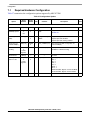
1
Block Diagram
3
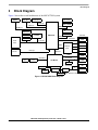
Block Diagram
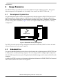
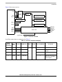
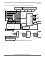
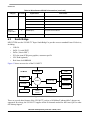
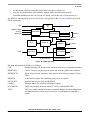
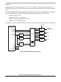
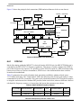
Figure 1 shows the overall architecture of the MPC8572DS system
SGMII
PCIe Slot 1
PCIe Slot 2
VTT Power
PEX1 x4
DDR-2 DIMM
PEX2 x2
DDR-2
SGMII x4
VTT Power
NOR Flash
NAND Flash
DDR-2 DIMM
MPC8572
FSRAM
DDR-2
ATX I/O
Panel I/O
PromJet
SER
Local Bus
Actel
Pixis
RJ45
TSECs
Interrupt
Clocks
RJ45
Vitesse
PHY
RJ45
RJ45
PEX3 x2
Audio
PCI
PCI
32-bit Bus
Panel I/O
ULI M1575
AUD
2
USB
USB
KB
Panel I/O
IDE
LPC
SIO
2
PS/2
SATA
TPM
Note: TPM is no longer supported.
Figure 1. MPC8572DS Block Diagram
MPC8572 Development System User’s Guide, Rev. 1
Freescale Semiconductor
3