1
Programming Model
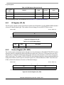
9.2.20
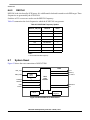
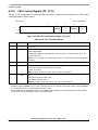
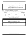
VELA DDRCLK[0:2] Registers (PX_VDDRCLK0/1/2)
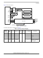
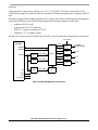
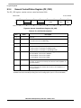
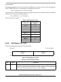
The PX_VDDRCLK[0:2] registers control the 24-bit configuration word of the ICS307 system clock
generator.
Offset
Access: Read/Write
0x1F (MSB)
0x20 (midbyte)
0x21 (LSB)
0
7
R
WORD
W
Reset
X
X
X
X
X
X
X
X
Figure 44. VELA VDDRCLK[0:2] Register (PX_VDDRCLK0/1/2)
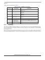
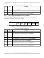
Table 50. PX_VDDRCLK[0:2] Field Descriptions
Bits
Name
Description
0–7
WORD
Read:returns the current programmed values.
Write: values written to WORD are driven into the ICS307 during reset sequencing if
PX_VCFGEN0[CLK]=1; otherwise, the encoded value of CFG_DDRCLK(0:2) is used.
Note: CFG_DDRCLK(0:2) are used to preset 24bits of data for the ICS307.
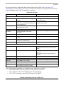
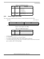
9.2.21
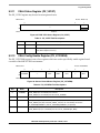
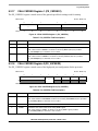
VELA Watchdog Register (PX_VWATCH)
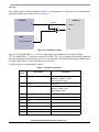
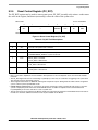
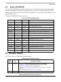
The PX_VWATCH register controls the duration of the watchdog facility.
Offset 0x24
Access: Read/Write
0
7
R
WTIME
W
Reset
0
1
1
1
1
1
1
1
Figure 45. VELA Watchdog Register (PX_VWATCH)
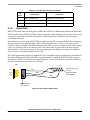
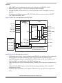
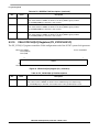
Table 51. PX_VWATCH Field Descriptions
Bits
Name
0–7
V
Description
Read:returns the current watchdog setting.
Write: sets new watchdog timer value. PX_VCTL[WDEN] must be zero (watchdog disabled) before
new values are written.
The PX_VWATCH register value represents the 8 most-significant bits of the 34 bit watchdog timer. Any
new value should be written before the PX_VCTL[WDEN] bit is set to one, and the value must be written
after every reset of this register (it resets just like any other general register).
MPC8572 Development System User’s Guide, Rev. 1
Freescale Semiconductor
69