1
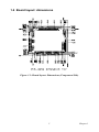
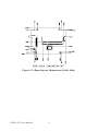
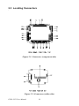
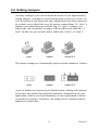
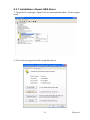
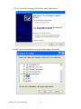
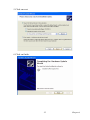
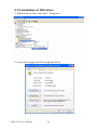
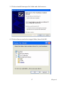
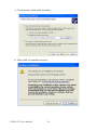
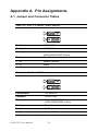
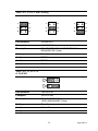
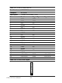
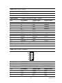
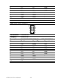
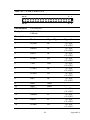
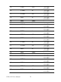
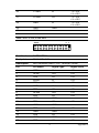
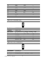
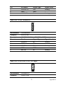
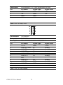
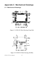
PCM-3353
PC/104+ SBC w/AMD LX800,
VGA, LCD, LAN, USB2.0 and CF
User Manual
Copyright
This document is copyrighted, © 2006. All rights are reserved. The original manufacturer reserves the right to make improvements to the products
described in this manual at any time without notice.
No part of this manual may be reproduced, copied, translated or transmitted in any form or by any means without the prior written permission of
the original manufacturer. Information provided in this manual is
intended to be accurate and reliable. However, the original manufacturer
assumes no responsibility for its use, nor for any infringements upon the
rights of third parties that may result from such use.
Acknowledgements
Award is a trademark of Award Software International, Inc.
VIA is a trademark of VIA Technologies, Inc.
IBM, PC/AT, PS/2 and VGA are trademarks of International Business
Machines Corporation.
Intel, Pentium, Celeron, and MMX are registered trademarks of Intel Corporation.
Microsoft Windows® is a registered trademark of Microsoft Corp.
RTL is a trademark of Realtek Semi-Conductor Co., Ltd.
ESS is a trademark of ESS Technology, Inc.
UMC is a trademark of United Microelectronics Corporation.
SMI is a trademark of Silicon Motion, Inc.
Creative is a trademark of Creative Technology LTD.
All other product names or trademarks are properties of their respective
owners.
For more information on this and other Advantech products, please visit
our websites at:
http://www.advantech.com
http://www.advantech.com/eplatform
For technical support and service, please visit our support website at:
http://www.advantech.com/support
This manual is for the PCM-3353.
Part No. 2006335311
2nd Edition
Printed in Taiwan
PCM-3353 User Manual
June 2008
ii
Packing List
Before you begin installing your card, please make sure that the following
materials have been shipped:
• 1 x PCM-3353 SBC
• 1 x Power cable (p/n:1700002332)
• 1 x Audio cable (p/n:1700000918)
• 1 x Four COM cable (p/n:1701400181)
• 1 x Keyboard/Mouse cable (p/n:1703060053)
• 1 x Y cable (for KB/MS extension) (p/n:1700060202)
• 1 x Ethernet RJ-45 Conn. conversion cable (p/n:1701100202)
• 1 x LPT port cable (p/n:1700260250)
• 1 x IDE cable (p/n:1701440350)
• 1 x VGA cable (p/n:1700000898)
• 2 x USB cable (bracket type with two USB ports) (p/n: 1703100121)
• 1 x Startup manual
• 1 x CD-ROM (Manual, Driver, Utility)
If any of these items are missing or damaged, contact your distributor or
sales representative immediately.
Model No. List
PCM-3353F-L0A1E
Description
PC/104+ SBC w/AMD LX800, VGA, LVDS,
LAN, USB and CF
PCM-3353Z-L0A1E
PCM-3353F-L0A1E with Phoenix Gold package
PCM-3353Z2-L0A1E PCM-3353F-L0A1E with Phoenix Platinum
package
iii
Additional Information and Assistance
1.Visit the Advantech web site at www.advantech.com where you can
find the latest information about the product.
2.Contact your distributor, sales representative, or Advantech's customer
service center for technical support if you need additional assistance.
Please have the following information ready before you call:
• Product name and serial number
• Description of your peripheral attachments
• Description of your software (operating system, version, application
software, etc.)
• A complete description of the problem
• The exact wording of any error messages
PCM-3353 User Manual
iv
This device complies with the requirements in part
15 of the FCC rules: Operation is subject to the following two conditions:
1.This device may not cause harmful interference,
and
2.This device must accept any interference
received, including interference that may cause
undesired operation
This equipment has been tested and found to comply with the limits for a Class A digital device, pursuant to Part 15 of the FCC Rules. These limits are
designed to provide reasonable protection against
harmful interference when the equipment is operated in a commercial environment. This equipment
generates, uses, and can radiate radio frequency
energy and, if not installed and used in accordance
with the instruction manual, may cause harmful
interference to radio communications. Operation of
this device in a residential area is likely to cause
harmful interference in which case the user will be
required to correct the interference at his/her own
expense. The user is advised that any equipment
changes or modifications not expressly approved
by the party responsible for compliance would void
the compliance to FCC regulations and therefore,
the user's authority to operate the equipment.
Caution!
Achtung!
There is a danger of a new battery exploding if it is
incorrectly installed. Do not attempt to recharge,
force open, or heat the battery. Replace the battery
only with the same or equivalent type recommended by the manufacturer. Discard used batteries according to the manufacturer’s instructions
v
PCM-3353 User Manual
vi
Contents
Chapter
1 Introduction ......................................................2
1.1
1.2
1.3
Introduction ....................................................................... 2
Features ............................................................................. 2
Specifications .................................................................... 2
1.3.1
1.3.2
1.3.3
1.3.4
1.3.5
1.3.6
1.4
Standard PC/104 Biscuit SBC Functions........................ 2
VGA/LVDS Interface ..................................................... 3
Ethernet Interface............................................................ 3
Audio Function ............................................................... 3
OS support ...................................................................... 3
Mechanical and Environmental ...................................... 4
Board layout: dimensions.................................................. 5
Figure 1.2:Board layout: Dimensions (Solder Side)....... 6
Chapter
2 Installation ........................................................8
2.1
Jumpers.............................................................................. 8
2.2
Connectors......................................................................... 8
2.3
Locating Connectors ....................................................... 10
Table 2.1:Jumper/Switch Setting:................................... 8
Table 2.2:Connector Table: ............................................ 8
Figure 2.1:Connectors (component side)...................... 10
Figure 2.2:Connectors (solder side).............................. 10
2.4
2.5
2.6
Setting Jumpers ............................................................... 11
Installing SO-DIMMs ..................................................... 12
IDE, CDROM hard drive connector (CN11) .................. 12
2.6.1
2.7
2.7.1
2.8
2.9
2.10
Connecting the hard drive............................................. 12
Solid State Disk............................................................... 13
Compact Flash (CN41) ................................................. 13
Parallel port connector (CN19) ....................................... 13
Keyboard and PS/2 mouse connector (CN18) ................ 13
Power connectors (CN38) ............................................... 13
2.10.1 Main power connector, +5 V, +12 V (CN38)............... 13
2.10.2 Power Reset button ....................................................... 13
2.11
Audio interfaces (CN34/35) ............................................ 14
2.11.1 Audio connector Audio-out(CN35), Audio-in(CN34) . 14
2.12
COM port connector (CN20,CN30)................................ 14
2.12.1 Serial Port RS-422/485 (CN20).................................... 14
Table 2.3:Serial Port RS-422/485 (CN39).................... 14
2.13
VGA/LCD interface connections .................................... 14
2.13.1 CRT display connector (CN27) .................................... 14
2.13.2 TTL TFT LCD connector (CN4) .................................. 14
2.13.3 LVDS TFT LCD connector (CN42)............................. 15
vii
2.14
Ethernet configuration..................................................... 15
2.15
2.16
2.17
Watchdog timer configuration ........................................ 15
USB connectors (CN15,CN17) ....................................... 15
GPIO (General Purpose Input Output) (CN36/CN37).... 16
2.14.1 100Base-T connector (CN26)....................................... 15
Chapter
3 Award BIOS Setup.........................................18
3.1
Introduction ..................................................................... 18
3.1.1
CMOS RAM Auto-backup and Restore ....................... 18
3.2
Entering Setup ................................................................. 19
3.3
3.4
3.5
Standard CMOS Setup .................................................... 20
Standard CMOS Setup ................................................... 20
Advanced BIOS Features ................................................ 20
Figure 3.1:Award BIOS Setup initial screen ................ 19
3.5.1
3.5.2
3.5.3
3.5.4
3.5.5
3.5.6
3.5.7
3.5.8
3.6
Integrated Peripherals...................................................... 22
3.6.1
3.6.2
3.6.3
3.6.4
3.6.5
3.6.6
3.6.7
3.6.8
3.6.9
3.7
Figure 3.2:Advanced BIOS features screen.................. 21
Virus Warning............................................................... 21
First/Second/Third/Other Boot Device......................... 21
Boot Up NumLock Status............................................. 21
Gate A20 Option........................................................... 21
Typematic Rate Setting................................................. 21
Typematic Rate (Chars/Sec) ......................................... 22
Typematic Delay (msec)............................................... 22
Security Option ............................................................. 22
IDE Master/Slave PIO/UDMA Mode,.......................... 22
Integrated peripherals screen ........................................ 23
Onboard LAN Control .................................................. 23
IDE HDD Block Mode ................................................. 23
Onboard Serial Port ...................................................... 23
Onboard Parallel Port.................................................... 23
Parallel Port Mode ........................................................ 23
EPP Mode Select .......................................................... 24
ECP Mode Use DMA ................................................... 24
Power Management Setup............................................... 24
3.7.1
3.7.2
3.7.3
3.7.4
3.7.5
3.7.6
3.7.7
3.7.8
3.7.9
3.7.10
PCM-3353 User Manual
Figure 3.3:Power management setup screen................. 24
ACPI function ............................................................... 24
Power Management ...................................................... 24
Video Off In Suspend ................................................... 25
Modem Use IRQ........................................................... 25
HDD Power Down........................................................ 25
PowerOn By Modem .................................................... 25
PowerOn By Alarm ...................................................... 25
Primary IDE 0 (1) and Secondary IDE 0 (1) ................ 25
FDD, COM, LPT PORT ............................................... 25
PCI PIRQ [A-D]# ......................................................... 25
viii
3.8
PnP/PCI Configurations .................................................. 26
3.8.1
3.8.2
3.8.3
3.8.4
3.9
PC Health Status.............................................................. 27
3.9.1
3.10
3.11
3.12
Chapter
Introduction ..................................................................... 30
4.1.1
4.1.2
4.1.3
4.2
4.3
AMD Geode LX ........................................................... 31
Table 4.1:Connections to Sharp LQ121S1DG31 / PCM3353 .................................................................. 31
Installation of the SVGA Driver ..................................... 32
4.3.1
4.3.2
4.3.3
4.4
Display type ................................................................. 30
Dual Simultaneous Display ......................................... 30
CMOS setting for panel type ....................................... 30
Connections to Two Standard LCDs............................... 31
4.2.1
Installation chipset AES driver ..................................... 33
Installation of VGA driver............................................ 36
PCI Bridge .................................................................... 40
Further Information ......................................................... 42
5 Audio Setup.....................................................44
5.1
5.2
Introduction ..................................................................... 44
Driver installation............................................................ 44
5.2.1
5.2.2
Chapter
PC Health Status Screen ............................................... 27
Password Setting ............................................................. 27
Save & Exit Setup ........................................................... 28
Exit Without Saving ........................................................ 28
4 PCI SVGA/LCD Setup ..................................30
4.1
Chapter
PnP OS Installed ........................................................... 26
Figure 3.4:PnP/PCI configurations screen.................... 26
Reset Configuration Data.............................................. 26
Resources controlled by:............................................... 26
PCI/VGA Palette Snoop ............................................... 26
Before you begin........................................................... 44
Windows XP drivers..................................................... 45
6 Ethernet Interface ..........................................50
6.1
6.2
Introduction ..................................................................... 50
Installation of Ethernet driver ......................................... 50
6.2.1
6.3
Installation for Windows XP ........................................ 51
Further information ......................................................... 56
Appendix A
Pin Assignments ............................................58
A.1
Jumper and Connector Tables ......................................... 58
Table A.1:SW1, CF Master / Slave Selector ................ 58
Table A.2:J3, Clear CMOS........................................... 58
Table A.3:CN39, COM2 Setting .................................. 59
Table A.4:J5, PCI VI/O POWER ................................. 59
Table A.5:CN42, LVDS LCD I/F................................. 60
ix
Table A.6:CN38, Power Input ...................................... 60
Table A.7:CN4, TFT LCD I/F ...................................... 61
Table A.8:CN5, Inverter Power.................................... 63
Table A.9:CN6, SMBus................................................ 63
Table A.10:CN32, Reset / Buzzer pin header............... 64
Table A.11:CN36, GPIO1 ............................................ 64
Table A.12:CN37, GPIO2 ............................................ 65
Table A.13:CN11, IDE ................................................. 65
Table A.14:CN27, CRT ................................................ 67
Table A.15:CN15, USB1/2........................................... 67
Table A.16:CN17, USB3/4........................................... 68
Table A.17:CN30, COM1/2/3/4 ................................... 69
Table A.18:CN19, Print Port ........................................ 71
Table A.19:CN20, RS422/485...................................... 72
Table A.20:CN35, AUDIO-OUT ................................. 72
Table A.21:CN34, AUDIO-IN ..................................... 73
Table A.22:CN23, ISA -5V & -12V Input ................... 73
Table A.23:CN26, LAN1.............................................. 74
Table A.24:CN18, KB/MS ........................................... 74
Table A.25:CN40, DDR RAM SOCKET..................... 75
Table A.26:CN41, CF SOCKET .................................. 75
Appendix B
System Assignments ......................................78
B.1
System I/O Ports.............................................................. 78
B.2
1st MB memory map....................................................... 79
B.3
DMA channel assignments.............................................. 79
B.4
Interrupt assignments ...................................................... 80
Table B.1:System I/O ports .......................................... 78
Table B.2:1st MB memory map ................................... 79
Table B.3:DMA channel assignments .......................... 79
Table B.4:Interrupt assignments ................................... 80
Appendix C Mechanical Drawings.....................................82
C.1
Mechanical Drawings...................................................... 82
Figure C.1:PCM-3353 Mech Drawing (Comp Side).... 82
Figure C.2:PCM-3353 Mech Drawing (Sol Side) ........ 82
PCM-3353 User Manual
x
CHAPTER
1
General Information
This chapter gives background information on the PCM-3353.
Sections include:
• Introduction
• Features
• Specifications
• Board layout and dimensions
Chapter 1 Introduction
1.1 Introduction
The PCM-3353 is a fanless, best-cost, performance PC/104+ SBC (Single
Board Computer) geared to satisfy the needs for various industrial computing equipment. PCM-3353 is ideal for communication, gaming and medical
applications that require flat panel support using digital displays with TTL
and LVDS interfaces and single Ethernet ports.
For those who want superior performance for various low-power embedded applications, PCM-3353 uses an AMD LX-800 processor clocked at
500 MHz, in conjunction with onboard DDR333 system memory.
PCM-3353 offers convenient connector layout, easy assembly, multiple I/
O, and includes single 10/100Mbps Ethernet, four USB (Universal Serial
Bus) 2.0 and four serial ports for easy system expansibility.
1.2 Features
• AMD low power LX800 500MHz Processor
• Supports DDR memory
• Supports 24-bit TFT LCD interface
• Supports 18-bit LVDS interface
• Supports 1 x 100Base-T Fast Ethernet
• Supports Four USB2.0 ports
• Supports Four COM ports
• PC/104+ expansion interface
1.3 Specifications
1.3.1 Standard PC/104 Biscuit SBC Functions
• CPU: AMD Geode® LX800 processor, up to 500 MHz
• System Memory: Onboard Memory, support Double Data Rate (DDR)
SDRAM, accept 128/256 MB, DDR333 SDRAM
• 2nd Cache Memory: 128 KB on the processor
• System Chipset: AMD Geode LX800
PCM-3353 User Manual
2
• BIOS: AWARD 4Mbit Flash BIOS
• Watchdog timer: 255 levels timer interval
• Expansion Interface: PC/104+
• Battery: Lithium 3V/196 mAH
• Power management: ACPI supported
• Enhanced IDE interface: One channel supports up to
two EIDE devices. BIOS auto-detect, PIO Mode 3 or
Mode 4, supports UDMA 33/66 mode
• Serial ports: Four serial RS-232 ports in one 40 pin connector (CN30:
COM1/2/3/4). RS-422 and RS-485 in one pinheader (CN20) and
can be configured via CN39 connector.
• Parallel port: One parallel port, supports SPP/EPP/ECP mode
• Keyboard/mouse connector: Supports one standard PC/AT keyboard
and a PS/2 mouse
• Audio: Supports AC97 Audio stereo sound
• USB: Four USB 2.0 ports compliant universal serial bus ports
• CF: Solid State Disk (SSD) supports one 50-pin socket for CFC type I
(type II optional)
1.3.2 VGA/LVDS Interface
• Chipset: AMD Geode LX800
• Memory Size: Optimized Shared Memory Architecture, supports 64 MB frame
buffer using system memory
• Resolution: CRT resolution: up to 1600 x 1200 x 16 bpp at 100 Hz and
up to 1024 x 768 x 32 bpp at 60 Hz for TFT LCD
• LCD Interface: Supports up to 24-bit TFT LCD (TTL signal)
Supports 18-bit LVDS LCD
• Dual Simultaneous Display: CRT + LCD, CRT + LVDS
1.3.3 Ethernet Interface
• Chipset supports: 1 x 10/100 Mbps - Intel 82551ER
• Interface: 1 x internal box header
• Standard IEEE 802.3u (100 BASE-T) protocol compatible
1.3.4 Audio Function
• Audio controller: Realtek ACL202/ACL650 chipset, supports AC97
3D Audio stereo sound
• Audio interface: Microphone in, Line in, Line out
1.3.5 OS support
• This board supports Win XP, Win CE and Win XPe.
3
Chapter 1
• For further information about OS support in your PCM-3353, visit the
following web resource Advantech: website: www.advantech.com or
please contact technical support center
1.3.6 Mechanical and Environmental
• Dimensions: 96 x 115 mm (3.77"x 4.05")
Mechanical Drawing (dxf file) is available.
• Power Supply Type: AT
• Power Requirement: +5 V ± 5%, +12 V ± 5% (Optional), (5V only,
12V optional for PC104 add on card and LCD inverter)
• Power Consumption:
(Geode LX800, 256 MB DDR333)
Max: +5 V @ 1.51 A, +12 V @ 0.1 A
Typical: +5 V @ 1.35 A, +12 V @ 0.1A
• Operating temperature: 0 ~ 60°C
(32 ~ 140°F)
• Operating Humidity: 10% ~ 90% relative humidity, non-condensing
• Weight: 0.85 kg (reference weight of total package)
PCM-3353 User Manual
4
1.4 Board layout: dimensions
Figure 1.1: Board layout: Dimensions (Component Side)
5
Chapter 1
Figure 1.2: Board layout: Dimensions (Solder Side)
PCM-3353 User Manual
6
CHAPTER
2
Installation
This chapter explains the setup procedures of the PCM-3353 hardware,
including instructions on setting jumpers and connecting peripherals,
switches and indicators. Be sure to read
all safety precautions before you begin
the installation procedure.
Chapter 2 Installation
2.1 Jumpers
The PCM-3353 has a number of jumpers that allow you to configure your
system to suit your application. The table below lists the functions of the
various jumpers.
Table 2.1: Jumper/Switch Setting:
J3
J5
CN39
SW1
Clear CMOS
PCI VI/O Power Selector
COM2 Setting
CF Master / Slave Selector
2.2 Connectors
Onboard connectors link the PCM-3353 to external devices such as hard
disk drives, a keyboard, or floppy drives. The table below lists the function of each of the board’s connectors.
Table 2.2: Connector Table:
CN4
CN5
CN6
CN11
CN15
CN18
CN19
CN20
CN23
CN26
CN27
CN30
CN32
CN35
CN36
CN38
CN40
CN41
TFT LCD I/F
Inverter Power
SMBus
IDE
USB1/2 / CN17 USB 3/4
KB/MS
Print Port
RS422/485
ISA -5V & -12V Input
LAN
CRT
COM1/2/3/4
Reset / Buzzer pin header
AUDIO-OUT / CN34 AUDIO-IN
GPIO1 / CN37 GPIO2
Power Input
DDR RAM Socket
CF Socket
PCM-3353 User Manual
8
CN42
CN43
LVDS LCD I/F
Inverter Power (LVDS)
9
Chapter 2
2.3 Locating Connectors
Figure 2.1: Connectors (component side)
Figure 2.2: Connectors (solder side)
PCM-3353 User Manual
10
2.4 Setting Jumpers
You may configure your card to match the needs of your application by
setting jumpers. A jumper is a metal bridge used to close an electric circuit. It consists of two metal pins and a small metal clip (often protected
by a plastic cover) that slides over the pins to connect them. To “close” a
jumper, you connect the pins with the clip. To “open” a jumper, you
remove the clip. Sometimes a jumper will have three pins, labeled 1, 2
and 3. In this case you would connect either pins 1 and 2, or 2 and 3.
open
closed
closed 2-3
The jumper settings are schematically depicted in this manual as follows:.
open
closed
closed 2-3
A pair of needle-nose pliers may be helpful when working with jumpers.
If you have any doubts about the best hardware configuration for your
application, contact your local distributor or sales representative before
you make any changes. Generally, you simply need a standard cable to
make most connections.
11
Chapter 2
2.5 Installing SO-DIMMs
The procedures for installing SODIMMs are described below. Please follow these steps carefully. You can install SDRAM memory modules
using 200-pin SODIMMs (Small Outline Dual In-line Memory Modules).
1. Ensure that all power supplies to the system are switched off.
2. Tilt the SODIMM card just above the board and slide it into the housing card slot.
3. Push the module into the socket until the module gently snaps in. There
should only be a slight insertion force to engage the module into the contacts. Make sure that the module and the housing are aligned and locked
in place.
2.6 IDE, CDROM hard drive connector (CN11)
The board provides 1 IDE channel which you can attach up to two
Enhanced Integrated Drive Electronics hard disk drives or CDROM to
the board’s internal controller. Its IDE controller uses a PCI interface.
This advanced IDE controller supports faster data transfer, PIO mode 3,
mode 4 and up to UDMA 33/66.
2.6.1 Connecting the hard drive
Connecting drives is done in a daisy-chain fashion. This package includes
One 44 PIN IDE cable that can connect to 1.8" and 2.5" drives.
1.
Connect one end of the cable to Hard Drive connector. Make sure
that the red (or blue) wire corresponds to pin 1 on the connector,
which is labeled on the board (on the right side).
2.
Plug the other end of the cable into the Enhanced IDE hard drive,
with pin 1 on the cable corresponding to pin 1 on the hard drive.
(See your hard drive’s documentation for the location of the connector.)
If desired, connect a second drive as described above.
Unlike floppy drives, IDE hard drives can connect to either end of the
cable. If you install two drives, you will need to set one as the master and
one as the slave by using jumpers on the drives. If you install only one
drive, set it as the master.
PCM-3353 User Manual
12
2.7 Solid State Disk
The board provides a CompactFlash card type I socket and type II for
optional kit.
2.7.1 Compact Flash (CN41)
The CompactFlash card shares a secondary IDE channel which can be
enabled/disabled via the BIOS settings.
2.8 Parallel port connector (CN19)
Normally, the parallel port is used to connect the cable to a printer. The
board includes a multi-mode (ECP/EPP) parallel port accessed via CN19
and a 26-pin flat-cable connector. You will need an adapter cable if you
use a traditional DB-25 connector. The adapter cable has a 26-pin connector on one end, and a DB-25 connector on the other.
The parallel port is designated as LPT1, and can be disabled or changed to
LPT2 or LPT3 in the system BIOS setup.
The parallel port interrupt channel is designated to be IRQ7.
You can select ECP/EPP/ECP DMA channel via BIOS setup.
2.9 Keyboard and PS/2 mouse connector (CN18)
The board provides a keyboard connector that supports both a keyboard
and a PS/2 style mouse. In most cases, especially in embedded applications, a keyboard is not used. If the keyboard is not present, the standard
PC/AT BIOS will report an error or fail during power-on self-test (POST)
after a reset. The PCM 3353’s BIOS standard setup menu allows you to
select “All, But Keyboard” under the “Halt On” selection. This allows
no-keyboard operation in embedded system applications, without the system halting under POST.
2.10 Power connectors (CN38)
2.10.1 Main power connector, +5 V, +12 V (CN38)
Supplies main power +5V to the PCM-3353, and to devices that require
+12 V.
2.10.2 Power Reset button
13
Chapter 2
Momentarily pressing the reset button will activate a reset. The switch
should be rated for 10 mA, 5 V.
2.11 Audio interfaces (CN34/35)
2.11.1 Audio connector Audio-out(CN35), Audioin(CN34)
The board provides all major audio signals on a 8-pin cable connector,
These audio signals include Microphone in (mono), Line in (stereo) and
Line out (stereo).
2.12 COM port connector (CN20,CN30)
The board provides four serial ports: Four serial RS-232 ports in one 40
pin connector (CN30: COM1/2/3/4). It provides connections for serial
devices or a communication network. You can find the pin assignments
for the COM port connector in Appendix C.
2.12.1 Serial Port RS-422/485 (CN20)
Serial port can be configured to operate in RS-422 and RS-485 mode. RS422 and RS-485 in one pinheader (CN20) and can be configured via
CN39 connector.
Table 2.3: Serial Port RS-422/485 (CN39)
Setting
Function
1-2
RS-232
3-4
RS-485
5-6
RS-422
2.13 VGA/LCD interface connections
The board’s PCI SVGA interface can drive conventional CRT displays
and is capable of driving a wide range of flat panel displays.
2.13.1 CRT display connector (CN27)
The CRT display connector is a 15-pin D-SUB connector used for conventional CRT displays.
2.13.2 TTL TFT LCD connector (CN4)
PCM-3353 User Manual
14
For PCM-3353 series, CN4 consists of a 40-pin connector which can support up to 24-bit LCD panel. It is Hirose’s product no. DF13A-40DP-1.25
V
2.13.3 LVDS TFT LCD connector (CN42)
Four PCM-3353 series, the board supports 1 channel 18-bit LVDS LCD
panel displays.
2.14 Ethernet configuration
The board is equipped with one high performance 32-bit PCI-bus Ethernet interface which are fully compliant with IEEE 802.3U 10/100Mbps
standards. They are supported by all major network operating systems.
2.14.1 100Base-T connector (CN26)
100Base-T connections are made via one internal 10-pin box header.
2.15 Watchdog timer configuration
An onboard watchdog timer reduces the chance of disruptions which
EMP (electro-magnetic pulse) interference can cause. This is an invaluable protective device for standalone or unmanned applications. Setup
involves one jumper and running the control software (refer to Appendix
A).
2.16 USB connectors (CN15,CN17)
The board provides up to four USB (Universal Serial Bus) ports using
Plug and Play. The USB interfaces comply with High Speed USB specification Rev. 2.0 which supports 480 Mbps transfer rate, and are fuse protected.
The USB interface is accessed through two 5 x 2-pin flat-cable connectors. You will need an adapter cable if you use a standard USB connector.
The adapter cable has a 5 x 2-pin connector on one end and a USB connector on the other.
The USB interfaces can be disabled in the system BIOS setup.
15
Chapter 2
2.17 GPIO (General Purpose Input Output) (CN36/
CN37)
The board supports 8-bit GPIO through GPIO connector. The 8 digital
inputs and outputs can be programmed to read or control devices, with
each input or output defined. The default setting is 8 bits input.
PCM-3353 User Manual
16
CHAPTER
3
Award BIOS Setup
17
Chapter 3
Chapter 3 Award BIOS Setup
3.1 Introduction
Award’s BIOS ROM has a built-in setup program that allows users to
modify the basic system configuration. This type of information is stored
in battery-backed memory (CMOS RAM) so that it retains the setup
information when the power is turned off.
3.1.1 CMOS RAM Auto-backup and Restore
The CMOS RAM is powered by an onboard button cell battery. When
you finish BIOS setup, the data in CMOS RAM will be automatically
backed up to Flash ROM. If operation in harsh industrial environments
causes a software error, the BIOS will recheck the data in CMOS RAM
and automatically restore the original data in Flash ROM to CMOS RAM
for booting.
Note:
If you intend to change the CMOS setting without restoring the previous backup, you have to
click on "DEL" within two seconds of the
"CMOS checksum error..." display screen message appearing. Then enter the "Setup" screen
to modify the data. If the "CMOS checksum
error..." message appears again and again,
please check to see if you need to replace the
battery in your system.
PCM-3353 User Manual
18
3.2 Entering Setup
Turn on the computer and check for the “patch code”. If there is a number
assigned to the patch code, it means that the BIOS supports your CPU.
If there is no number assigned to the patch code, please contact Advantech’s applications engineer to obtain an up-to-date patch code file. This
will ensure that your CPU’s system status is valid. After ensuring that you
have a number assigned to the patch code, press <Del> to allow you to
enter the setup.
Figure 3.1: Award BIOS Setup initial screen
19
Chapter 3
3.3 Standard CMOS Setup
Choose the “Standard CMOS Features” option from the “Initial Setup
Screen” menu, and the screen below will be displayed. This menu allows
users to configure system components such as date, time, hard disk drive,
Video, Halt On, display, and memory.
3.4 Standard CMOS Setup
3.5 Advanced BIOS Features
The “Advanced BIOS Features” screen appears when choosing the
“Advanced BIOS Features” item from the “Initial Setup Screen” menu. It
allows the user to configure the board according to his particular requirements. Below are some major items that are provided in the Advanced
BIOS Features screen. A quick booting function is provided for your con-
PCM-3353 User Manual
20
venience. Simply enable the Quick Booting item to save yourself valuable time.
Figure 3.2: Advanced BIOS features screen
3.5.1 Virus Warning
If enabled, a warning message and alarm beep activates if someone
attempts to write here. The commands are “Enabled” or “Disabled.”
3.5.2 First/Second/Third/Other Boot Device
The BIOS tries to load the OS with the devices in the sequence selected.
Choices are: HDD, CDROM, LAN, Disabled.
3.5.3 Boot Up NumLock Status
This feature selects the “power on” state for NumLock. The commands
are “Enabled” or “Disabled.”
3.5.4 Gate A20 Option
Normal:
A pin in keyboard controller controls GateA20
Fast (Default):
Chipset controls GateA20.
3.5.5 Typematic Rate Setting
The typematic rate is the rate key strokes repeat as determined by the keyboard controller. The commands are “Enabled” or “Disabled.” Enabling
allows the typematic rate and delay to be selected.
21
Chapter 3
3.5.6 Typematic Rate (Chars/Sec)
BIOS accepts the following input values (characters/second) for typematic rate: 6, 8, 10, 12, 15, 20, 24, 30.
3.5.7 Typematic Delay (msec)
Typematic delay is the time interval between the appearance of two consecutive characters, when holding down a key. The input values for this
category are: 250, 500, 750, 1000 (msec).
3.5.8 Security Option
This setting determines whether the system will boot up if the password is
denied. Access to Setup is always limited.
System
The system will not boot, and access to Setup will be denied
if the correct password is not entered at the prompt.
Setup
The system will boot, but access to Setup will be denied if
the correct password is not entered at the prompt.
Note:
To disable security, select “PASSWORD SETTING” in the main menu. At this point, you will
be asked to enter a password. Simply press
<Enter> to disable security. When security is
disabled, the system will boot, and you can
enter Setup freely.
3.6 Integrated Peripherals
3.6.1 IDE Master/Slave PIO/UDMA Mode,
IDE Master/Slave PIO/UDMA Mode (Auto) has a master and a slave,
making two IDE devices possible. Because each IDE device may have a
different Mode timing (0, 1, 2, 3, 4), it is necessary for these to be independent. The default setting “Auto” will allow auto detection to ensure
optimal performance.
PCM-3353 User Manual
22
3.6.2 Integrated peripherals screen
3.6.3 Onboard LAN Control
Options are Enable or Disable. Select Disable if user does not want to use
onboard LAN controller1
3.6.4 IDE HDD Block Mode
You can enable the Primary IDE channel and/or the Secondary IDE channel. Any channel not enabled is disabled. This field is for systems with
only SCSI drives.
3.6.5 Onboard Serial Port
For settings reference the Appendix for the serial resource allocation,
and Disabled for the on-board serial connector
3.6.6 Onboard Parallel Port
This field sets the address of the onboard parallel port connector. You can
select either 3BCH/IRQ7, 378H/IRQ7, 278H/IRQ5 or Disabled. If you
install an I/O card with a parallel port, make sure there is no conflict in
the address assignments. The CPU card can support up to three parallel
ports, as long as there are no conflicts for each port.
3.6.7 Parallel Port Mode
This field allows you to set the operation mode of the parallel port. The
setting “Normal” allows normal speed operation, but in one direction
only. “EPP” allows bidirectional parallel port operation at maximum
speed. “ECP” allows the parallel port to operate in bi-directional mode
and at a speed faster than the maximum data transfer rate. “ECP + EPP”
allows normal speed operation in a two-way mode.
23
Chapter 3
3.6.8 EPP Mode Select
This field allows you to select EPP port type 1.7 or 1.9.
3.6.9 ECP Mode Use DMA
This selection is available only if you select “ECP” or “ECP + EPP” in
the Parallel Port Mode field. In ECP Mode Use DMA, you can select
DMA channel 1, DMA channel 3, or Disable. Leave this field on the
default setting.
3.7 Power Management Setup
The power management setup controls the CPU card’s “green” features to
save power. The following screen shows the manufacturer’s defaults:
Figure 3.3: Power management setup screen
3.7.1 ACPI function
The choice: Enabled, Disabled.
3.7.2 Power Management
This category allows you to select the type (or degree) of power saving
and is directly related to the following modes:
1. HDD Power Down
2. Suspend Mode
PCM-3353 User Manual
24
There are four selections for Power Management, three of which have
fixed mode settings
Min. Power Saving
Minimum power management., Suspend Mode = 1 hr.,
and HDD Power Down = 15 min.
Max. Power Saving
Maximum power management., Suspend Mode = 1 min.,
and HDD Power Down = 1 min.
User Defined
(Default)
Allows you to set each mode individually. When not disabled, each of the ranges are from 1 min. to 1 hr. except
for HDD Power Down which ranges from 1 min. to 15 min.
and disable.
3.7.3 Video Off In Suspend
When system is in suspend, video will turn off.
3.7.4 Modem Use IRQ
This determines the IRQ which the MODEM can use. The choices: 3, 4,
5, 7, 9, 10, 11, NA.
3.7.5 HDD Power Down
You can choose to turn the HDD off after one of the time intervals listed,
or when the system is in “suspend” mode. If the HDD is in a power saving mode, any access to it will wake it up.
3.7.6 PowerOn By Modem
When Enabled, an input signal on the serial Ring Indicator (RI) line (in
other words, an incoming call on the modem) awakens the system from a
soft off state. The choices: Enabled, Disabled.
3.7.7 PowerOn By Alarm
When Enabled, your can set the date and time at which the RTC (realtime clock) alarm awakens the system from Suspend mode. The choices:
Enabled, Disabled.
3.7.8 Primary IDE 0 (1) and Secondary IDE 0 (1)
When Enabled, the system will resume from suspend mode if Primary
IDE 0 (1) or Secondary IDE 0 (1) is active. The choices are: Enabled,
Disabled.
3.7.9 FDD, COM, LPT PORT
When Enabled, the system will resume from suspend mode if FDD, COM
port, or LPT port is active. The choice: Enabled, Disabled.
3.7.10 PCI PIRQ [A-D]#
25
Chapter 3
When Enabled, the system will resume from suspend mode if an interrupt
occurs. The choices are: Enabled, Disabled.
3.8 PnP/PCI Configurations
3.8.1 PnP OS Installed
Select Yes if you are using a plug and play capable operating system.
Select No if you need the BIOS to configure non-boot device
Figure 3.4: PnP/PCI configurations screen
3.8.2 Reset Configuration Data
Default is Disable. Select Enable to reset Extended System Configuration
Data (ESCD) if you have installed a new add-on and system configuration has caused such a conflict that OS cannot boot.
3.8.3 Resources controlled by:
The commands here are “Auto” or “Manual.” Choosing “manual”
requires you to choose resources from each following sub-menu. “Auto”
automatically configures all of the boot and Plug and Play devices but
you must be using Windows 95 or above.
3.8.4 PCI/VGA Palette Snoop
This is left at “Disabled.”
PCM-3353 User Manual
26
3.9 PC Health Status
This is to check the PC health, e.g.: current CPU temperature.
3.9.1 PC Health Status Screen
3.10 Password Setting
To change the password:
1.
Choose the “Set Password” option from the “Initial Setup Screen”
menu and press <Enter>.
The screen will display the following message
Please Enter Your Password
Press <Enter>.
2.
If the CMOS is good or if this option has been used to change the
default password, the user is asked for the password stored in the CMOS.
The screen will display the following message:
27
Chapter 3
Please Confirm Your Password
Enter the current password and press <Enter>.
3.
After pressing <Enter> (ROM password) or the current password
(user-defined), you can change the password stored in the CMOS. The
password must be no longer than eight (8) characters.
Remember, to enable the password setting feature, you must first select
either “Setup” or “System” from the “Advanced BIOS Features” menu.
3.11 Save & Exit Setup
If you select this and press <Enter>, the values entered in the setup utilities will be recorded in the CMOS memory of the chipset. The microprocessor will check this every time you turn your system on and compare
this to what it finds as it checks the system. This record is required for the
system to operate.
3.12 Exit Without Saving
Selecting this option and pressing <Enter> lets you exit the setup program
without recording any new values or changing old ones.
PCM-3353 User Manual
28
CHAPTER
4
PCI SVGA/LCD Setup
This chapter details the software configuration information. It shows you
how to configure the card to match
your application requirements. The
AWARD System BIOS is covered in
Chapter 4.
Sections include:
• Installation of SVGA drivers
-for Window XP
• Connections for standard LCDs
• Further information
Chapter 4 PCI SVGA/LCD Setup
4.1 Introduction
The board has an onboard AMD Geode LX800 chipset for its PCI/SVGA
controller. It supports TFT LCD displays and conventional analog CRT
monitors with 64MB frame buffer shared with system memory. The VGA
controller can drive CRT displays with resolutions up to 1600 x 1200 x 16
bpp at 100 Hz and up to 1024 x 768 x 32 bpp at 60 Hz for TFT LCD.
4.1.1 Display type
The board can be set in one of three configurations: on a CRT, on a flat
panel display, or on dual simultaneous display. The system is initially set
to dual display mode. If you want to enable the CRT display only or the
flat panel display only, please set them up from the BIOS screen, or, contact Advantech technical support center.
4.1.2 Dual Simultaneous Display
The board uses a AMD LX800 controller that is capable of providing
multiple views and simultaneous display with mixed video and graphics
on a flat panel and CRT. The Dual display can be set up by CMOS setting.
4.1.3 CMOS setting for panel type
The board system BIOS and custom drivers are located in a 512 KB,
Flash ROM device. A single Flash chip holds the system BIOS, VGA
BIOS and network Boot ROM image. The display can be configured via
CMOS settings. This method minimized the number of chips and different type of LCD panels, please choose "panel type" from the "Advanced
Chipset Features" menu in CMOS setting.
PCM-3353 User Manual
30
4.2 Connections to Two Standard LCDs
Connector Table of 12.1" TTL Sharp LQ121S1DG31 800 x 600 5/3.3V
(18 Bit) for PCM-3353 AMD Geode LX.
4.2.1 AMD Geode LX
Table 4.1: Connections to Sharp LQ121S1DG31 / PCM-3353
Sharp LQ121S1DG31
PCM-3353
DF9MA-41P-1V
DF-13 4OP-1.25V
Pin
Function
Pin
1
GND
3
GND
2
CK
35
DOTCLK
3
GND
4
GND
4
Hsync
38
HS
5
Vsync
36
VS
6
GND
7
GND
8
GND
8
GND
Function
9
R0
27
D18
10
R1
28
D19
11
R2
29
D20
12
GND
13
R3
30
D21
14
R4
31
D22
15
R5
32
D23
16
GND
17
GND
18
GND
19
G0
19
D10
20
G1
20
D11
21
G2
21
D12
22
GND
23
G3
22
D13
24
G4
23
D14
25
G5
24
D15
26
GND
33
GND
31
Chapter 4
Table 4.1: Connections to Sharp LQ121S1DG31 / PCM-3353
27
GND
28
GND
33
GND
29
B0
11
D2
30
B1
12
D3
31
B2
13
D4
32
GND
34
GND
33
B3
14
D5
34
B4
15
D6
35
B5
16
D7
36
GND
34
GND
37
ENAB
37
DE
38
NC
39
VCC
5
+3.3 V
40
VCC
6
+3.3 V
41
NC
* The polarity of both synchronous signals are negative.
4.3 Installation of the SVGA Driver
Complete the following steps to install the SVGA driver. Follow the procedures in the flow chart that apply to the operating system that you are
using within your board.
Notes:
1. The windows illustrations in this chapter are intended
as examples only. Please follow the listed steps, and pay
attention to the instructions which appear on your screen.
2. For convenience, the CD-ROM drive is designated as
"D" throughout this chapter.
PCM-3353 User Manual
32
4.3.1 Installation chipset AES driver
1. Open device manager, right click on entertainment then, click on properties
2. Go to driver page and click on update driver.
33
Chapter 4
3. Click on install from specific folder and click on next.
4.Click on browse and select target folder, then, click OK.
PCM-3353 User Manual
34
5.Click on next.
6.Click on finish.
35
Chapter 4
4.3.2 Installation of VGA driver
1. Right click on video, and click “ Properties”.
2. Go to driver page and click on update driver.
PCM-3353 User Manual
36
3. Click on install from specific folder and click on next.
4. Click on browse and select target folder, then click OK.
37
Chapter 4
5. Click on next, then click on finish.
6. Then click on continue anyway.
PCM-3353 User Manual
38
7. Click on finish.
39
Chapter 4
4.3.3 PCI Bridge
The system may detect PCI bridge automatically. If the question mark is
shown on device manager, please install the driver as below:
1. Click “Add Hardware Wizard” and add new hardware wizard
PCM-3353 User Manual
40
2. Search the right directory of PCI bridge for IT8888G driver.
41
Chapter 4
3. Installation finished.
4.4 Further Information
For further information about the AGP/VGA installation of your PCM3353, including driver updates, troubleshooting guides and FAQ lists,
visit the following web resources:
Intel website: www.intel.com
Advantech websites: www.advantech.com
www.advantech.com.tw
PCM-3353 User Manual
42
CHAPTER
5
Audio Setup
The board is equipped with an audio
interface that records and plays back
CD-quality audio. This chapter provides instructions for installing the software drivers included on the audio
driver diskettes.
Chapter 5 Audio Setup
5.1 Introduction
The onboard audio interface provides high-quality stereo sound by using
the AMD LX800 audio controller. The audio interface can record, compress, and play back voice, sound, and music with built-in mixer control.
5.2 Driver installation
5.2.1 Before you begin
Please read the instructions in this chapter carefully before you attempt
installation. The audio drivers for the board are located on the audio
driver CD. Run the supplied SETUP program to install the drivers; don’t
copy the files manually.
Note:
The files on the software installation diskette
are compressed. Do not attempt to install the
drivers by copying the files manually. You must
use the supplied SETUP program to install the
drivers.
PCM-3353 User Manual
44
5.2.2 Windows XP drivers
1.
Open device manager, right click on audio and click on “properties”.
2.
Go to driver page and click on update driver.
45
Chapter 5
3.
Click on install from specific folder and click on next.
4.
Click on browse and select target folder, then click OK.
PCM-3353 User Manual
46
5.
Click on next.
6.
Click on continue anyway.
47
Chapter 5
7.
Click on finish.
PCM-3353 User Manual
48
CHAPTER
6
Ethernet Interface
This chapter provides information on
Ethernet configuration.
Sections include:
• Introduction
• Installation of Ethernet drivers for
Windows XP
• Further information
Chapter 6 Ethernet Interface
6.1 Introduction
The board is equipped with a high performance 32-bit Ethernet chipset
which is fully compliant with IEEE 802.3 100 Mbps CSMA/CD standards. It is supported by major network operating systems. With
100Base-T compatible. The network boot feature can be utilized by
incorporating the boot ROM image files for the appropriate network
operating system. The boot ROM BIOS files are combined with system
BIOS, which can be enabled/disabled in the BIOS setup.
6.2 Installation of Ethernet driver
Before installing the Ethernet driver for Intel 82551ER chipset, note the
procedures below. You must know which operating system you are using
with your board, and then refer to the corresponding installation flow
chart, just follow the steps described in the flow chart.
Note:
The windows illustrations in this chapter are
examples only. Follow the steps and pay attention to the instructions which appear on your
screen.
PCM-3353 User Manual
50
6.2.1 Installation for Windows XP
1.
a. Select "Start", "Settings". "Control Panel".
b. Double click "Network".
51
Chapter 6
2.
Click “Add new hardware wizard” and prepare to install network
function
PCM-3353 User Manual
52
3.
Choose Hardware Device “Ethernet Controller”
53
Chapter 6
4.
Insert the CD into D: drive
a. Fill in the Find the LAN chipset folder at the directory of PCM-3353
win2000 folder from CD ROM drive
b. Click “OK”.
PCM-3353 User Manual
54
5.
Choose the "Intel® GD82559ER PCI Adapter" item
Click “Next”
55
Chapter 6
6
a. Make sure the configurations of relative items are set correctly
b. Click “OK”
6.3 Further information
Intel website: www.intel.com
Advantech websites:www.advantech.com
www.advantech.com.tw
PCM-3353 User Manual
56
Appendix
A
Pin Assignments
This appendix contains information
of a detailed or specialized nature. It
includes:
Appendix A Pin Assignments
A.1 Jumper and Connector Tables
Table A.1: SW1, CF Master / Slave Selector
Part Number
1600000071
Footprint
JH2X1V-2M
Description
PIN HEADER 2*1P
180D (M)SQUARE 2.0mm
Setting
Function
(1 - 2)
Master (default)
(2 - 3)
Slave
Table A.2: J3, Clear CMOS
Part Number
1653003101
Footprint
JH3X1V-2M
Description
PIN HEADER 3*1P
180D (M)SQUARE 2.0mm
Setting
Function
(1 - 2)
BAT (default)
(2 - 3)
Clear-CMOS
PCM-3353 User Manual
58
Table A.3: CN39, COM2 Setting
1
2
1
2
1
2
3
4
3
4
3
4
5
6
5
6
5
6
Part Number
1653003201
Footprint
JH3X2S-2M
Description
PIN HEADER 3*2P 180D SMDMALE
SQUARE PIN 2.0mm
Setting
Function
(1 - 2)
RS232
(3 - 4)
RS485
(5 - 6)
RS422
Table A.4: J5, PCI VI/
O POWER
Part Number
1653003101
Footprint
JH3X1V-2M
Description
PIN HEADER 3*1P
180D (M)SQUARE 2.0mm
Setting
Function
(1 - 2)
With +5V
(2 - 3)
With +3.3V
59
Appendix A
Table A.5: CN42, LVDS LCD I/F
Part Number
1653910261
Footprint
SPH10x2
Description
*CONN. DF13-20DP-1.25V
Pin
Pin Name
Signal Type
1
GND
GND
2
GND
GND
3
D0+
I/O
4
NONE
5
D0-
6
NONE
7
D1+
8
NONE
9
D1-
10
NONE
11
D2+
12
NONE
13
D2-
14
NONE
15
CLK+
16
NONE
17
CLK-
Signal Level
I/O
I/O
I/O
I/O
I/O
I/O
I/O
18
NONE
19
+5V/+3.3V
PWR
+5V/+3.3V
20
+5V/+3.3V
PWR
+5V/+3.3V
Table A.6: CN38, Power Input
8
1
PCM-3353 User Manual
60
Part Number
1655308020
Footprint
PWR-B4PV
Description
PIN HEADER DIP 8*1P 180D(M) 2.00mm
Pin
Pin Name
Signal Type
Signal Level
1
+5V
PWR
+5V
2
+5V
PWR
+5V
3
+5V
PWR
+5V
4
GND
GND
-
5
GND
GND
-
6
GND
GND
-
7
GND
GND
-
8
+12V
PWR
+12V
Table A.7: CN4, TFT LCD I/F
39 37
3
1
40 38
4
2
Part Number
1653920200
Footprint
SPH20X2
Description
*CONN. DF13-40DP-1.25V
Pin
Pin Name
Signal Type
Signal Level
1
+5V
PWR
+5V
2
+5V
PWR
+5V
3
GND
GND
-
4
GND
GND
-
5
+3.3V
PWR
+3.3V
6
+3.3V
PWR
+3.3V
7
TV-CLK
CLK48M
+3.3V
8
GND
GND
-
9
D0
I/O
+3.3V
10
D1
I/O
+3.3V
61
Appendix A
11
D2
I/O
+3.3V
12
D3
I/O
+3.3V
13
D4
I/O
+3.3V
14
D5
I/O
+3.3V
15
D6
I/O
+3.3V
16
D7
I/O
+3.3V
17
D8
I/O
+3.3V
18
D9
I/O
+3.3V
19
D10
I/O
+3.3V
20
D11
I/O
+3.3V
21
D12
I/O
+3.3V
22
D13
I/O
+3.3V
23
D14
I/O
+3.3V
24
D15
I/O
+3.3V
25
D16
I/O
+3.3V
26
D17
I/O
+3.3V
27
D18
I/O
+3.3V
28
D19
I/O
+3.3V
29
D20
I/O
+3.3V
30
D21
I/O
+3.3V
31
D22
I/O
+3.3V
32
D23
I/O
+3.3V
33
GND
GND
-
34
GND
GND
-
35
DOTCLK
CLK
+3.3V
36
VS
OUT
+3.3V
37
DE
I/O
+3.3V
38
HS
OUT
+3.3V
39
RST
OUT
+3.3V
40
FP
OUT
+3.3V
PCM-3353 User Manual
62
Table A.8: CN5, Inverter Power
5
4
3
2
1
Part Number
1655305020
Footprint
WHL5V-2M
Description
WAFER BOX 2.0mm 5P 180D MALE W/LOCK
Pin
Pin Name
1
2
3
ENABKL
OUT
+3.3V
4
VBR
OD
+3.3V
5
+5V
PWR
+5V
Signal Type
Signal Level
+12V
PWR
+12V
GND
GND
-
Table A.9: CN6, SMBus
2
1
Part Number
1653002101
Footprint
JH2X1V-2M
Description
PIN HEADER 2*1P 180D (M)SQUARE 2.0mm
Pin
Pin Name
Signal Type
Signal Level
1
SMB-CLK
CLK
+3V
2
SMB-DAT
I/O
+3V
63
Appendix A
Table A.10: CN32, Reset / Buzzer pin header
6
4
2
5
3
1
Part Number
1653002201
Footprint
WHL2V-2M
Description
PIN HEADER DIP 2*2P
Pin
Pin Name
Signal Type
Signal Level
1
-
-
-
2
-
-
-
3
GND
GND
-
4
RST
IN
+3.3V
5
Buzzer -
-
-
6
Buzzer +
-
-
180D(M) 2.00mm
Table A.11: CN36, GPIO1
5
4
3
2
1
Part Number
1653010100
Footprint
JH5X2S-2M
Description
PIN HEADER SMD 5*1P 180D(M) 2.54mm
Pin
Pin Name
Signal Type
Signal Level
1
+5V
PWR
+5V
2
GPIO0
I/O
+5V
3
GPIO1
I/O
+5V
4
GPIO2
I/O
+5V
5
GPIO3
I/O
+5V
PCM-3353 User Manual
64
Table A.12: CN37, GPIO2
5
4
3
2
1
Part Number
1653010100
Footprint
JH5X2S-2M
Description
PIN HEADER SMD 5*1P 180D(M) 2.54mm
Pin
Pin Name
Signal Type
Signal Level
1
GPIO4
I/O
+5V
2
GPIO5
I/O
+5V
3
GPIO6
I/O
+5V
4
GPIO7
I/O
+5V
5
GND
-
-
Table A.13: CN11, IDE
Part Number
1653222262
Footprint
BH22X2SV
Description
BOX HEADER SMD 22*2P 180D(M) 2.0mm IDIOT-PROOF
Pin
Pin Name
Signal Type
1
RST#
Out
+5V
2
GND
GND
-
3
D7
I/O
+5V
4
D8
I/O
+5V
5
D6
I/O
+5V
6
D9
I/O
+5V
7
D5
I/O
+5V
65
Signal Level
Appendix A
8
D10
I/O
+5V
9
D4
I/O
+5V
10
D11
I/O
+5V
11
D3
I/O
+5V
12
D12
I/O
+5V
13
D2
I/O
+5V
14
D13
I/O
+5V
15
D1
I/O
+5V
16
D14
I/O
+5V
17
D0
I/O
+5V
18
D15
I/O
+5V
19
GND
GND
-
21
DREQ
Out
+5V
22
GND
GND
-
23
IOW#
Out
+5V
24
GND
GND
-
25
IOR#
Out
+5V
26
GND
GND
-
27
IORDY
Out
+5V
28
CSEL#
Out
+5V
29
DACK#
Out
+5V
30
GND
GND
-
31
IRQ14
In
+5V
32
NC
-
-
33
A1
In
+5V
34
D66DET#
In
+5V
35
A0
In
+5V
36
A2
In
+5V
37
CS#1
Out
+5V
38
CS#3
Out
+5V
39
ASP#
Out
+5V
40
GND
GND
-
41
+5V
PWR
+5V
42
+5V
PWR
+5V
43
GND
GND
-
44
NC
-
-
PCM-3353 User Manual
66
Table A.14: CN27, CRT
Part Number
1655912120
Footprint
DBVGA-VF5M
Description
CONN. 12P 90D(F) SMD 1.25mm
Pin
Pin Name
Signal Type
Signal Level
1
GND
GND
-
2
R
OUT
Analog
3
G
OUT
Analog
4
B
OUT
Analog
5
GND
GND
-
6
+5V
PWR
-
7
DDAT
OD I/O
+3.3V
8
DCLK
OD I/O
+3.3V
9
GND
GND
-
10
HSYNC
OUT
+3.3V
11
VSYNC
OUT
+3.3V
12
GND
-
-
Table A.15: CN15, USB1/2
10
5
9
8
4
3
7
2
6
1
Part Number
1653005260
Footprint
JH5X2S-2M
Description
PIN HEADER 5*2P 180D(M) 2.0mm SMD IDIOT-PROOF
Pin
Pin Name
Signal Type
Signal Level
1
+5V
PWR
+5V
2
+5V
PWR
+5V
3
P0-
I/O
USB
67
Appendix A
4
P1-
I/O
USB
5
P0+
I/O
USB
6
P1+
I/O
USB
7
GND
GND
-
8
GND
GND
-
9
GND
GND
-
10
NC
-
-
Table A.16: CN17, USB3/4
10
5
9
8
4
3
7
2
6
1
Part Number
1653005260
Footprint
JH5X2S-2M
Description
PIN HEADER 5*2P 180D(M) 2.0mm SMD IDIOT-PROOF
Pin
Pin Name
Signal Type
Signal Level
1
+5V
PWR
+5V
2
+5V
PWR
+5V
3
P2-
I/O
USB
4
P3-
I/O
USB
5
P2+
I/O
USB
6
P3+
I/O
USB
7
GND
GND
-
8
GND
GND
-
9
GND
GND
-
10
NC
-
-
PCM-3353 User Manual
68
Table A.17: CN30, COM1/2/3/4
39 37
3
1
40 38
4
2
Part Number
1653220260
Footprint
BH20X2SV2.00mm
Description
Pin
Pin Name
Signal Type
Signal Level
1
DCD#1
IN
-3~-12V,
+3~+12V
2
DSR#1
IN
-3~-12V,
+3~+12V
3
RXD1
IN
-3~-12V,
+3~+12V
4
RTS#1
I/O
-3~-12V,
+3~+12V
5
TXD1
OUT
-3~-12V,
+3~+12V
6
CTS#1
IN
-3~-12V,
+3~+12V
7
DTR#1
I/O
-3~-12V,
+3~+12V
8
RI#1
IN
-3~-12V,
+3~+12V
9
GND
GND
-
10
GND
GND
-
11
DCD#2
In
-3~-12V,
+3~+12V
12
DSR#2
In
-3~-12V,
+3~+12V
13
RXD2
In
-3~-12V,
+3~+12V
14
RTS#2
I/O
-3~-12V,
+3~+12V
69
Appendix A
15
TXD2
Out
-3~-12V,
+3~+12V
16
CTS#2
In
-3~-12V,
+3~+12V
17
DTR#2
I/O
-3~-12V,
+3~+12V
18
RI#2
In
-3~-12V,
+3~+12V
19
GND
GND
-
20
GND
GND
-
21
DCD#3
In
-3~-12V,
+3~+12V
22
DSR#3
In
-3~-12V,
+3~+12V
23
RXD3
In
-3~-12V,
+3~+12V
24
RTS#3
I/O
-3~-12V,
+3~+12V
25
TXD3
Out
-3~-12V,
+3~+12V
26
CTS#3
In
-3~-12V,
+3~+12V
27
DTR#3
I/O
-3~-12V,
+3~+12V
28
RI#3
In
-3~-12V,
+3~+12V
29
GND
GND
-
30
GND
GND
-
31
DCD#4
In
-3~-12V,
+3~+12V
32
DSR#4
In
-3~-12V,
+3~+12V
33
RXD4
In
-3~-12V,
+3~+12V
34
RTS#4
I/O
-3~-12V,
+3~+12V
35
TXD4
Out
-3~-12V,
+3~+12V
PCM-3353 User Manual
70
36
CTS#4
In
-3~-12V,
+3~+12V
37
DTR#4
I/O
-3~-12V,
+3~+12V
38
RI#4
In
-3~-12V,
+3~+12V
39
GND
GND
-
40
GND
-
-
Table A.18: CN19, Print Port
25 23
3 1
26 24
4 2
Part Number
1653213260
Footprint
BH13x2SV-2.00
Description
BOX HEADER SMD 13*2P 180D(M) 2.0mm
Pin
Pin Name
1
STB#
Out
+5V
2
AFD#
Out
+5V
3
PD0
I/O
+5V
4
ERR#
In
+5V
5
PD1
I/O
+5V
6
INIT#
Out
+5V
7
PD2
I/O
+5V
8
SLIN#
Out
+5V
9
PD3
I/O
+5V
10
GND
GND
-
11
PD4
I/O
+5V
12
GND
GND
-
Signal Type
Signal Level
13
PD5
I/O
+5V
14
GND
GND
-
15
PD6
I/O
+5V
16
GND
GND
-
17
PD7
I/O
+5V
71
Appendix A
18
GND
GND
-
19
ACK#
In
+5V
20
GND
GND
-
21
BUSY
In
+5V
22
GND
GND
-
23
PE
In
+5V
24
GND
GND
-
25
SLCT
In
+5V
26
NC
-
-
Table A.19: CN20, RS422/485
4
3
2
1
Part Number
1653004101
Footprint
JH4X1V-2M
Description
PIN HEADER 4*1P 180D(M) SQUARE 2.0mm
Pin
Pin Name
Signal Type
Signal Level
1
422-RXD-
In
+5V
2
422-RXD+
In
+5V
3
485-422-TXD+
Out
+5V
4
485-422-TXD-
Out
+5V
Table A.20: CN35, AUDIO-OUT
3
2
1
Part Number
1655303120
Footprint
WHL3V-2M
Description
WAFER BOX 2.0mm 3P 180D w/LOCK
PCM-3353 User Manual
72
Pin
Pin Name
Signal Type
Signal Level
1
LIN-OUT-R
OUT
Analog
2
GND
GND
-
3
LIN-OUT-L
Out
Analog
Table A.21: CN34, AUDIO-IN
5
4
3
2
1
Part Number
16553050202
Footprint
WHL3V-2M
Description
WAFER BOX 2.0mm 3P 180D w/LOCK
Pin
Pin Name
Signal Type
Signal Level
1
LIN-IN-R
IN
Analog
2
GND
GND
-
3
LIN-IN-L
IN
Analog
4
GND
GND
-
5
MIC-IN
IN
Analog
Table A.22: CN23, ISA -5V & -12V Input
3
2
1
Part Number
1653003101
Footprint
JH3X1V-2M
73
Appendix A
Description
PIN HEADER 3*1P 180D (M)SQUARE 2.0mm
Pin
Pin Name
Signal Type
Signal Level
1
-12V
PWR
-12V
2
-5V
PWR
-5V
3
GND
GND
-
Table A.23: CN26, LAN1
10
5
9
8
4
3
7
2
6
1
Part Number
1653205260
Footprint
BH5X2SV
Description
BOX HEADER SMD 5*2 180D (M) 2.0mm
Pin
Pin Name
Signal Type
Signal Level
1
+3.3V
PWR
+3.3V
2
LAN2-ACTLED
IN
Analog
3
LAN2-RX+
IN
Analog
4
LAN2-RX-
IN
Analog
5
LAN2-LILED
IN
Analog
6
LAN2-LCT
I/O
Analog
7
N/A
-
-
8
LAN2-LCT
I/O
Analog
9
LAN2-TX+
OUT
Analog
10
LAN2-TX-
OUT
Analog
Table A.24: CN18, KB/MS
PCM-3353 User Manual
74
6
5
4
3
2
1
Part Number
1655306020
Footprint
BH5X2SV
Description
BOX HEADER DIP 6*1 180D (M) 2.0mm
Pin
Pin Name
Signal Type
Signal Level
1
KB-CLK
IN
+5V
2
KB-DATA
IN
+5V
3
MS-CLK
IN
+5V
4
GND
PWR
-
5
+5V
PWR
+5V
6
MS-DATA
IN
+5V
Table A.25: CN40, DDR RAM SOCKET
Part Number
1651000051
Footprint
Description
SODIMM 200P DDR SMD
Table A.26: CN41, CF SOCKET
Part Number
1653025211
Footprint
JH5X2S-2M
Description
HEADER 50P 90D
75
Appendix A
PCM-3353 User Manual
76
Appendix
B
System Assignments
This appendix contains information of a detailed
nature. It includes:
• System I/O ports
• 1st MB memory map
• DMA channel assignments
• Interrupt assignments
Appendix B System Assignments
B.1 System I/O Ports
Table B.1: System I/O ports
Addr. range (Hex)
Device
000-01F
020-021
040-05F
060-06F
070-07F
DMA controller
Interrupt controller 1, master
8254 timer
8042 (keyboard controller)
Real-time clock, non-maskable interrupt (NMI)
mask
080-09F
DMA page register
0A0-0BF
Interrupt controller 2
0C0-0DF
DMA controller
0F0
Clear math co-processor
0F1
Reset math co-processor
0F8-0FF
Math co-processor
1F0-1F8
Fixed disk
200-207
Reserved (Game I/O)
278-27F
Reserved (Parallel port 2,LTP3)
2E8-2EF
Reserved (Series port 4)
2F8-2FF
Serial port 2
300-31F
Prototype card
360-36F
Reserved
378-37F
Parallel printer port 1 (LPT 2)
380-38F
SDLC, bisynchronous 2
3A0-3AF
Bisynchronous 1
3B0-3BF
Monochrome display and printer adapter (LPT1)
3C0-3CF
Reserved
3D0-3DF
Color/graphics monitor adapter
3E8-3EF
Reserved (Series port 3)
3F0-3F7
Diskette controller
3F8-3FF
Serial port 1
* PNP audio I/O map range from 220 ~ 250H (16 bytes)
MPU-401 select from 300 ~ 330H (2 bytes)
PCM-3353 User Manual
78
B.2 1st MB memory map
Table B.2: 1st MB memory map
Addr. range (Hex)
Device
F0000h - FFFFFh
*CC000h - EFFFFh
C0000h - CBFFFh
B8000h - BFFFFh
B0000h - B7FFFh
A0000h - AFFFFh
00000h - 9FFFFh
System ROM
Unused (reserved for Ethernet ROM)
Expansion ROM (for VGA BIOS)
CGA/EGA/VGA text
Unused
EGA/VGA graphics
Base memory
* If Ethernet boot ROM is disabled (Ethernet ROM occupies about 16 KB)
* E0000 - EFFFF is reserved for BIOS POST
B.3 DMA channel assignments
Table B.3: DMA channel assignments
Channel
Function
0
1
2
3
4
5
6
7
Available
Available (audio)
Floppy disk (8-bit transfer)
Available (parallel port)
Cascade for DMA controller 1
Available
Available
Available
* Audio DMA select 1, 3, or 5
** Parallel port DMA select 1 (LPT2) or 3 (LPT1)
79
Chapter B
B.4 Interrupt assignments
Table B.4: Interrupt assignments
Interrupt#
Interrupt source
IRQ 0
IRQ 1
IRQ 2
IRQ 3
IRQ 4
IRQ 5
IRQ 6
IRQ 7
IRQ 8
IRQ 9
IRQ 10
IRQ 11
IRQ 12
IRQ 13
IRQ 14
IRQ 15
Interval timer
Keyboard
Interrupt from controller 2 (cascade)
COM2
COM1
Reserved (COM4)
FDD
LPT1
RTC
Reserved (audio)
Reserved (COM3)
Reserved for watchdog timer
PS/2 mouse
INT from co-processor
Primary IDE
Secondary IDE for CFC
* Ethernet interface IRQ select: 9, 11, 15
* PNP audio IRQ select: 9, 11, 15
* PNP USB IRQ select: 9, 11, 15
* PNP ACPI IRQ select: 9, 11, 15
PCM-3353 User Manual
80
Appendix
C
Mechanical Drawings
Appendix C Mechanical Drawings
C.1 Mechanical Drawings
Figure C.1: PCM-3353 Mech Drawing (Comp Side)
Figure C.2: PCM-3353 Mech Drawing (Sol Side)
PCM-3353 User Manual
82