1
Recommended Resets
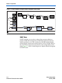
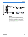
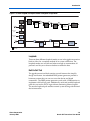
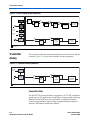
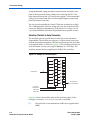
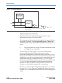
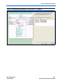
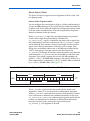
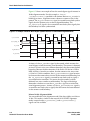
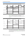
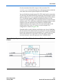
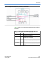
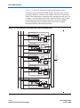
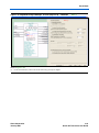
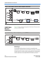
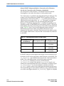
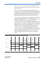
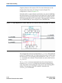
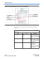
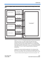
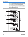
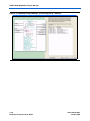
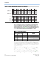
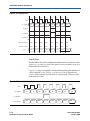
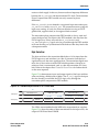
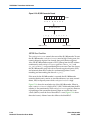
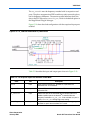
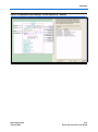
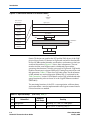
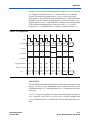
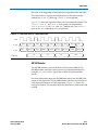
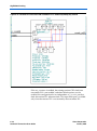
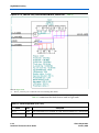
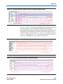
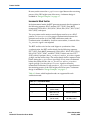
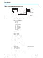
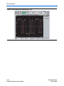
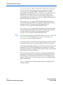
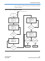
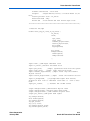
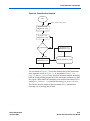
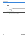
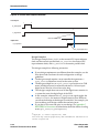
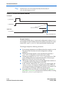
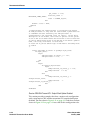
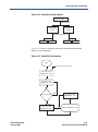
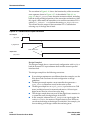
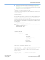
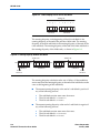
The waveform in Figure 9–4 shows the functionality of the receiver and
transmitter reset sequence shown in Figure 9–3. The pll_areset signal
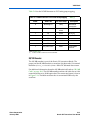
resets the entire transceiver block, including both the analog and digital
portions of the transmitter and receiver (see Table 9–1). After the
pll_areset signal goes low, the controller waits until the transmitter
PLL is stable (pll_locked = 1’b1) before sending the tx_digitalreset
and rx_analogreset low. This ensures that the output of the
transmitter PLL is stable before releasing any of the logic that it feeds. The
transmitter PLL clock in this case also trains the receiver PLL. After the
CRU has transitioned to locking to data from locking to the reference
clock, the rx_freqlocked signal goes high, which allows the CRU to
transition into the wait state where a timer is loaded a certain amount of
time. See the Stratix GX FPGA Family data sheet for the amount of time
loaded into the timer. When the timer counts down, rx_clkout is stable.
The reset controller then sends rx_digital low, completing the reset
sequence. You will be able to monitor the BER (for example, a
synchronization state machine based on the Stratix GX transceiver data)
to determine whether the system is initialized and working properly.
Figure 9–4. Receiver & Transmitter Reset Sequence Waveforms
Reset Signals
pll_areset
tx_digitalreset
rx_analogreset
rx_digitalreset
Stable Transmit
Pll Clock
Output Status Signals
Stable Recovered Clock
pll_locked
rx_freqlocked
Trx_freqlock2phaselock
9–6
Stratix GX Transceiver User Guide
Altera Corporation
January 2005