1
Appendix C. REFCLKB Pin
Constraints
Known Issues
This document discusses issues you might encounter in certain
configurations of the Stratix® GX device. These issues are a result of a
combination of resource utilization (REFCLKB pins that use Inter Quad
(IQ) lines, signals (pllenable, pll_areset, and rxanalogreset),
and software modeling.
The potential issues for certain configurations are described below:
1.
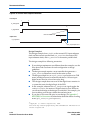
The pll_areset and pllenable signals in a transceiver block
reset its dedicated clock (REFCLKB) pad.
If the design uses the REFCLKB pin of the active transceiver block to
feed core logic, there is no clock to the core logic if the pll_areset
or pllenable signal is asserted. This problem could be severe if the
clock from the REFCLKB pin is also feeding the reset controller/logic
in the core logic. The system may never come out of reset in this
configuration.
Modeling in the Quartus® II software simulation does not reveal this
issue. This issue also exists for multiple transceiver block
applications that use the REFCLKB pin for clocking.
2.
Asserting the rxanalogreset signal of all four channels in a
transceiver block resets its dedicated clock pad.
This might happen if, in the design, only the receive portions of the
channels are used and the REFCLKB pin of the transceiver block is
used to feed the clock to the core logic. This can affect any logic using
the clock from this pad. This behavior is not modeled in the
Quartus II software simulation.
If the reference clock to the receiver (rx_cruclk) is routed globally,
the clock pad is not in use and will not flat-line the reference clock.
3.
Altera Corporation
January 2005
When the rxanalogreset signal of all four channels in a
transceiver block is asserted, it also resets the transmitter PLL.
C–1