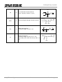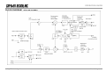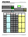
1
OPERATION GUIDE UHF Narrow band radio transceiver STD-302N-R 434MHz Operation Guide Version 1.5 (Feb. 2014) CIRCUIT DESIGN, INC., 7557-1 Hotaka, Azumino Nagano 399-8303 JAPAN Tel: + +81-(0)263-82-1024 Fax: + +81-(0)263-82-1016 e-mail: [email protected] http://www.cdt21.com OG_STD-302N-R_v15e OPERATION GUIDE CONTENTS GENERAL DESCRIPTION & FEATURES ...........................3 SPECIFICATIONS STD-302N-R 434 MHz .......................4 PIN DESCRIPTION .............................................................6 BLOCK DIAGRAM...............................................................8 DIMENSIONS......................................................................9 PLL IC CONTROL .............................................................10 PLL IC control ..................................................................10 How to calculate the setting values for the PLL register ........ 11 Method of serial data input to the PLL .................................12 TIMING CHART.................................................................13 PLL FREQUENCY SETTING REFERENCE .....................15 TEST DATA .......................................................................17 REGULATORY COMPLIANCE INFORMATION ................19 CAUTIONS & WARNINGS ................................................20 REVISION HISTORY.........................................................21 OG_STD-302N-R_v15e 2 Circuit Design, Inc. OPERATION GUIDE GENERAL DESCRIPTION & FEATURES General Description The UHF FM narrow band semi-duplex radio data module STD-302N-R is a R&TTE and RoHS compliant, high performance transceiver designed for use in industrial applications requiring long range, high performance and reliability. All high frequency circuits are enclosed inside a robust housing to provide superior resistance against shock and vibration. A narrow band technique enables high interference rejection and concurrent operation with multiple modules. STD-302N-R, a narrowband module with 25 kHz channel steps, achieves high TX/RX switching speed, making it an ideal RF unit for inclusion in feedback systems. Features 10 mW RF power, 3.0 V operation Programmable RF channel Fast TX/RX switching time High sensitivity -119 dBm Excellent mechanical durability, high vibration & shock resistance R&TTE (EN 300 220) / RoHS compliance Applications Telemetry Water level monitor for rivers, dams, etc. Monitoring systems for environmental data such as temperature, humidity, etc. Transmission of measurement data (pressure, revolution, current, etc) to PC Security alarm monitoring Telecontrol Industrial remote control systems Remote control systems for factory automation machines Control of various driving motors Data transmission RS232/RS485 serial data transmission OG_STD-302N-R_v15e 3 Circuit Design, Inc. OPERATION GUIDE SPECIFICATIONS STD-302N-R 434 MHz All ratings at 25 +/-10 °C unless otherwise noted General characteristics Item Applicable standard Communication method Emission class Operating frequency range Operation temperature range Storage temperature range Aging rate Initial frequency tolerance Dimensions Weight Units MHz °C °C ppm ppm mm g MIN TYP MAX EN 300 220 Simplex, Half-duplex F1D 433.050 434.775 -20 60 -30 75 -1 1 -1.5 1.5 30 x 50 x 9 mm 25 g Remarks No dew condensation No dew condensation TX freq., RX Lo freq. TX freq., RX Lo freq. Not including antenna Electrical specification <Common> Item Oscillation type Frequency stability (-20 to 60°C) TX/RX switching time Channel step Data rate Max. pulse width Min. pulse width Data polarity PLL reference frequency PLL response Antenna impedance Operating voltage TX consumption current RX consumption current ppm ms kHz bps ms us MHz ms Ω V mA mA MIN TYP MAX PLL controlled VCO -4 4 15 20 25 2400 9600 15 100 Positive 21.25 30 60 50 3.0 5.5 44 48 26 30 Remarks Reference frequency at 25 °C DI/DO DO/DI DO/DI DO/DI DO/DI TCXO from PLL setting to LD out Nominal Vcc = 3.0 V Vcc = 3.0 V Transmitter part Item RF output power Deviation DI input level Residual FM noise mW kHz V kHz Spurious emission dBm Adjacent CH power dBm OG_STD-302N-R_v15e MIN 2.35 0 TYP 10 2.75 MAX 3.15 5.5 0.17 -54 -36 -30 -37 4 Remarks Conducted 50 Ω PN9 9600 bps L= GND, H = 3 V- Vcc DI=L, LPF=20 kHz 47-74, 87.5-118, 174-230, 470-862 MHz Other frequencies below 1000 MHz Frequencies above 1000 MHz PN9 9600 bps CH25kHz/BW16kHz Circuit Design, Inc. OPERATION GUIDE Receiver part Item Receiver type 1st IF frequency 2nd IF frequency Maximum input level BER (0 error/2556 bits) *1 BER (1 % error) *2 Sensitivity 12dB/ SINAD MHz kHz dBm dBm dBm dBm Spurious response rejection *3 dB Adjacent CH selectivity *3 Intermodulation *4 DO output level dB dB V RSSI rising time ms Time until valid Data-out *5 ms Spurious radiation dBm RSSI mV MIN TYP MAX Double superheterodyne 21.7 450 10 -107 -110 -116 -119 80 60 50 50 0 2.8 30 50 50 70 50 100 70 120 -57 -47 180 230 280 Remarks At 434.05MHz PN 9 9600bps At 434.05MHz PN 9 9600bps fm1 k/ dev 2.75 kHz CCITT 1 st Mix, 2 signal method, 1 % error 2 nd Mix, 2 signal method, 1 % error +/- 25 kHz, 2 signal method, 1 % error 2 signal method, 1 % error L = GND H = 2.8 V CH shift of 25 kHz (from PLL setup) When power ON (from PLL setup) CH shift of 25 kHz (from PLL setup) When power ON (from PLL setup) Below 1000 MHz Above 1000 MHz With -113 dBm at 434.05MHz Specifications are subject to change without prior notice Notice The time required until a stable DO is established may get longer due to the possible frequency drift caused by operation environment changes, especially when switching from TX to RX, from RX to TX and changing channels. Please make sure to optimize the timing. The recommended preamble is more than 20 ms. Antenna connection is designed as pin connection. RF output power, sensitivity, spurious emission and spurious radiation levels may vary with the pattern used between the RF pin and the coaxial connection. Please make sure to verify those parameters before use. The feet of the shield case should be soldered to the wide GND pattern to avoid any change in characteristics. Notes about the specification values *1 BER: RF level where no error per 2556 bits is confirmed with the signal of PN9 and 9600 bps. *2 BER (1 % error) : RF level where 1% error per 2556 bits is confirmed with the signal of PN9 and 9600 bps. *3 Spurious response, CH selectivity: Jamming signal used in the measurement is unmodulated. *4 Intermodulation: Ratio between the receiver input level with BER 1% and the signal level (PN9 9600 bps) added at the points of 'Receiving frequency - 200 kHz ' + ' Receiving frequency -100kHz' with which BER 1% is achieved. *5 Time until valid Data-out : Valid DO is determined at the point where Bit Error Rate meter starts detecting the signal of 9600bps, 1010repeated signal. All specifications are specified based on the data measured in a shield room using the PLL setting controller board prepared by Circuit Design. Measuring equipment: SG=ANRITUS communication analyzer MT2605 Spectrum analyzer = ANRITSU MS2663G BER measure = ANRITSU MP1201G OG_STD-302N-R_v15e 5 Circuit Design, Inc. OPERATION GUIDE PIN DESCRIPTION Pin name I/O Description Equivalent circuit 47P SAW FILTER RF I/O RF RF input terminal Antenna impedance nominal 50 Ω 100nH GND GND I GROUND terminal The GND pins and the feet of the shield case shoud be connected to the wide GND pattern. VCC 2.8V VCC TXSEL I Power supply terminal DC 3.0 to 5.5 V I TX select terminal GND = TXSEL active To enable the transmitter circuits, connect TXSEL to GND and RXSEL to OPEN or 2.8 V. REG 22µ O Analogue output terminal There is DC offset of approx. 1 V. Refer to the specification table for amplitude level. MB15E03 I PLL data setting input terminal Interface voltage H = 2.8 V, L = 0 V MB15E03 DATA I PLL data setting input terminal Interface voltage H = 2.8 V, L = 0 V LE I PLL data setting input terminal Interface voltage H = 2.8 V, L = 0 V CLK OG_STD-302N-R_v15e 6 20K TXSEL I AF 47P 2.8V 10 2.8V RX select terminal GND= RXSEL active To enable the receiver circuits, connect RXSEL to GND and TXSEL to OPEN or 2.8 V. RXSEL 10µ 47P 2.8V 10 20K 2.8V RXSEL 2K CLK 2K DATA 2K LE MB15E03 Circuit Design, Inc. OPERATION GUIDE 2.8V LD O PLL lock/unlock monitor terminal Lock = H (2.8 V), Unlock = L (0 V) 2K LD MB15E03 102 RSSI O Received Signal Strength Indicator terminal 2.8V DO DI O I OG_STD-302N-R_v15e Data output terminal Interface voltage: H=2.8V, L=0V 10K 2K DO 102 Data input terminal Interface voltage: H=2.8V to Vcc, L=0V Input data pulse width Min.100 μs Max. 15 ms 7 Circuit Design, Inc. OPERATION GUIDE. BLOCK DIAGRAM OG_STD-302N-R_v15e <STD-302N-R 434MHz> 8 Circuit Design, Inc. OPERATION GUIDE. DIMENSIONS OG_STD-302N-R_v15e 9 Circuit Design, Inc. OPERATION GUIDE . PLL IC CONTROL PLL IC control Figure 1 up to 1200MHz VCO 2kohm Voltage Controled Oscillator Fin CLK Xf in Data 2kohm 2kohm LE GND LPF PLL Do +2.8v LE PS VCC ZC 2kohm 21.25MHz DATA MB15E03SL Vp Reference Oscillator CLK LD/f out OSCout P OSCin R LD STD-302 Control pin name #:Control v oltage = +2.8v STD-302N-R is equipped with an internal PLL frequency synthesizer as shown in Figure 1. The operation of the PLL circuit enables the VCO to oscillate at a stable frequency. Transmission frequency is set externally by the controlling IC. STD-302N-R has control terminals (CLK, LE, DATA) for the PLL IC and the setting data is sent to the internal register serially via the data line. Also STD-302N-R has a Lock Detect (LD) terminal that shows the lock status of the frequency. These signal lines are connected directly to the PLL IC through a 2 kΩ resistor. The interface voltage of STD-302N-R is 2.8 V, so the control voltage must be the same. STD-302N-R comes equipped with a Fujitsu MB15E03SL PLL IC. Please refer to the manual of the PLL IC. The following is a supplementary description related to operation with STD-302N-R. In this description, the same names and terminology as in the PLL IC manual are used, so please read the manual beforehand. OG_STD-302N-R_v15e 10 Circuit Design, Inc. OPERATION GUIDE . How to calculate the setting values for the PLL register The PLL IC manual shows that the PLL frequency setting value is obtained with the following equation. -- Equation 1 fvco = [(M x N)+A] x fosc / R fvco : Output frequency of external VCO M: Preset divide ratio of the prescaler (64 or 128) N: Preset divide ratio of binary 11-bit programmable counter (3 to 2,047) A: Preset divide ratio of binary 7-bit swallow counter (0 ≤ A ≤ 127 A<N)) fosc: Output frequency of the reference frequency oscillator R: Preset divide ratio of binary 14-bit programmable reference counter (3 to 16,383) With STD-302N-R, there is an offset frequency (foffset) 21.7 MHz for the transmission RF channel frequency fch. Therefore the expected value of the frequency generated at VCO (fexpect) is as below. fvco = fexpect = fch – foffset ---- Equation 2 The PLL internal circuit compares the phase to the oscillation frequency fvco. This phase comparison frequency (fcomp) must be decided. fcomp is made by dividing the frequency input to the PLL from the reference frequency oscillator by reference counter R. STD-302N-R uses 21.25 MHz for the reference clock fosc. fcomp is one of 6.25 kHz, 12.5 kHz or 25 kHz. The above equation 1 results in the following with n = M x N + A, where “n” is the number for division. n = fvco/fcomp ---- Equation 4 note: fcomp = fosc/R fvco=n*fcomp ---- Equation 3 Also, this PLL IC operates with the following R, N, A and M relational expressions. N = INT (n / M) ---- Equation 6 A = n - (M x N) ---- Equation 7 R=fosc/fcomp ---- Equation 5 INT: integer portion of a division. As an example, the setting value of RF channel frequency fch 869.725 MHz can be calculated as below. The constant values depend on the electronic circuits of STD-302N-R. Conditions: Channel center frequency: fch = 869.725 MHz Constant: Offset frequency: foffset=21.7 MHz Constant: Reference frequency: fosc=21.25 MHz Set 25 kHz for Phase comparison frequency and 64 for Prescaler value M The frequency of VCO will be fvco = fexpect = fch - foffset = 869.725 –21.7 = 848.025MHz Dividing value “n” is derived from Equation 4 n = fvco / fcomp = 848.025MHz/25kHz = 33921 Value “R” of the reference counter is derived from Equation 5. R = fosc/fcomp = 21.25MHz/25kHz = 850 Value “N” of the programmable counter is derived from Equation 6. N = INT (n/M) = INT(33921/64) = 530 Value “A“ of the swallow counter is derived from Equation 7. A = n – (M x N) = 33921 – 64 x 530 = 1 The frequency of STD-302N-R is locked at a center frequency fch by inputting the PLL setting values N, A and R obtained with the above equations as serial data. The above calculations are the same for the other frequencies. Excel sheets that contain automatic calculations for the above equations can be found on our web site (www.cdt21.com/). The result of the calculations is arranged as a table in the CPU ROM. The table is read by the channel change routine each time the channel is changed, and the data is sent to the PLL. OG_STD-302N-R_v15e 11 Circuit Design, Inc. OPERATION GUIDE . Method of serial data input to the PLL After the RF channel table plan is decided, the data needs to be allocated to the ROM table and read from there or calculated with the software. Together with this setting data, operation bits that decide operation of the PLL must be sent to the PLL. The operation bits for setting the PLL are as follows. These values are placed at the head of the reference counter value and are sent to the PLL. 1. CS: Charge pump current select bit CS = 0 +/-1.5 mA select VCO is optimized to +/-1.5 mA 2. LDS: LD/fout output setting bit LDS = 0 LD select Hardware is set to LD output 3. FC: Phase control bit for the phase comparator FC = 1 Hardware operates at this phase Figure 2 1st Data 2nd Data 2nd data N11 N10 N9 N8 N7 N6 A1 CNT=0 1st data CS LDS FC SW R14 R13 R1 CNT=1 Inv alid Data DATA MSB LSB CLK t1 t2 t6 t3 t0 LE STD-302 terminal name #: t0,t5 >= 100 ns t1,t2,t6 >= 20 ns t3,t4 >= 30 ns t4 t5 #: Keep the LE terminal at a low level, w hen w rite the data to the shift resister. The PLL IC, which operates as shown in the block diagram in the manual, shifts the data to the 19-bit shift register and then transfers it to the respective latch (counter, register) by judging the CNT control bit value input at the end. 1. CLK [Clock]: Data is shifted into the shift register on the rising edge of this clock. 2. LE [Load Enable]: Data in the 19-bit shift register is transferred to respective latches on the rising edge of the clock. The data is transferred to a latch according to the control bit CNT value. 3. Data [Serial Data]: You can perform either reference counter setup or programmable counter setup first. OG_STD-302N-R_v15e 12 Circuit Design, Inc. OPERATION GUIDE . TIMING CHART Control timing in a typical application is shown in Figure 3. Initial setting of the port connected to the radio module is performed when power is supplied by the CPU and reset is completed. MOS-FET for supply voltage control of the radio module, RXSEL and TXSEL are set to inactive to avoid unwanted emissions. The power supply of the radio module is then turned on. When the radio module is turned on, the PLL internal resistor is not yet set and the peripheral VCO circuit is unstable. Therefore data transmission and reception is possible 40 ms after the setting data is sent to the PLL at the first change of channel, however from the second change of channel, the circuit stabilizes within 20 ms and is able to handle the data. Changing channels must be carried out in the receive mode. If switching is performed in transmission mode, unwanted emission occurs. If the module is switched to the receive mode when operating in the same channel, (a new PLL setting is not necessary) it can receive data within 5 ms of switching*1. For data transmission, if the RF channel to be used for transmission is set while still in receiving mode, data can be sent at 5 ms after the radio module is switched from reception to transmission*2. Check that the Lock Detect signal is “high” 20 ms after the channel is changed. In some cases the Lock Detect signal becomes unstable before the lock is correctly detected, so it is necessary to note if processing of the signal is interrupted. It is recommended to observe the actual waveform before writing the process program. *1 DC offset may occur due to frequency drift caused by ambient temperature change. Under conditions below -10 °C, 10 to 20 ms delay of DO output is estimated. The customer is urged to verify operation at low temperature and optimize the timing. *2 Sending ‘10101…..’ preamble just after switching to transmission mode enables smoother operation of the binarization circuit of the receiver. For 9600 bps, a preamble of ‘11001100’ is effective. Preamble length: -20 °C - +60 °C: 15 ms (Typical) Remark For details about PLL control and the sample programs, see our technical document ‘STD-302 interface method’ OG_STD-302N-R_v15e 13 Circuit Design, Inc. OPERATION GUIDE Figure 3: Timing diagram for STD-302 Status immediately after pow er comes on. Normal status Channel change No channel change CPU Pow er on STD-302 Pow er on #:3 Receiv e mode Receiv e mode Receiv e mode activ e period activ e period activ e period Activ e period RXSEL CPU control, CH change & Data rec. Timing #:1 #:2 #:4 5 ms #:4 CH Data #:5 CH #:4 Data #:6 Check LD signal Check LD signal CH Data #:7 Check LD signal LD 40 ms 10 to 20 ms Transmit mode activ e TXSEL Transmit mode activ e Transmit mode activ e Data transmit 5 ms 5 ms #:1 Reset control CPU 5 ms #:5 40 ms later, the receiver can receive the data after changing the channel.. #:2 Initialize the port connected to the module. #:6 10 to 20 ms later, the receiver can receive the data after changing the channel. #:3 Supply pow er to the module after initializing CPU. #:7 5 ms later, the data can be received if the RF channel is not changed. #:4 RFchannel change must be performed in receiving mode. OG_STD-302N-R_v15e 14 Circuit Design, Inc. . OPERATION GUIDE PLL FREQUENCY SETTING DATA REFERENCE 434 MHz ISM band (433.050 - 434.790 MHz) Parameter name Phase Comparing Frequency Fcomp [kHz] Start Channel Frequency Fch [MHz] Channel Step Frequency [kHz] Number of Channel Prescaler M Parameter name Reference Frequency Fosc [MHz] Offset Frequency Foffset [MHz] No. Value : For data input 25 433.0750 25 69 64 : Result of calculation : Fixed value Parameter name Reference Counter R Programmable Counter N Min. Value Programmable Counter N Max. Value Swallow Counter A Min. Value Swallow Counter A Max. Value Value 21.25 21.7 Channel Frequency FCH Expect Frequency FEXPECT Lock Frequency FVCO (MHz) (MHz) (MHz) 433.0750 433.1000 433.1250 433.1500 433.1750 433.2000 433.2250 433.2500 433.2750 433.3000 433.3250 433.3500 433.3750 433.4000 433.4250 433.4500 433.4750 433.5000 433.5250 433.5500 433.5750 433.6000 433.6250 433.6500 433.6750 433.7000 433.7250 433.7500 433.7750 433.8000 433.8250 433.8500 433.8750 411.3750 411.4000 411.4250 411.4500 411.4750 411.5000 411.5250 411.5500 411.5750 411.6000 411.6250 411.6500 411.6750 411.7000 411.7250 411.7500 411.7750 411.8000 411.8250 411.8500 411.8750 411.9000 411.9250 411.9500 411.9750 412.0000 412.0250 412.0500 412.0750 412.1000 412.1250 412.1500 412.1750 411.3750 411.4000 411.4250 411.4500 411.4750 411.5000 411.5250 411.5500 411.5750 411.6000 411.6250 411.6500 411.6750 411.7000 411.7250 411.7500 411.7750 411.8000 411.8250 411.8500 411.8750 411.9000 411.9250 411.9500 411.9750 412.0000 412.0250 412.0500 412.0750 412.1000 412.1250 412.1500 412.1750 0 1 2 3 4 5 6 7 8 9 10 11 12 13 14 15 16 17 18 19 20 21 22 23 24 25 26 27 28 29 30 31 32 OG_STD-302N-R_v15e 15 Number of Division n 16455 16456 16457 16458 16459 16460 16461 16462 16463 16464 16465 16466 16467 16468 16469 16470 16471 16472 16473 16474 16475 16476 16477 16478 16479 16480 16481 16482 16483 16484 16485 16486 16487 Value 850 257 258 0 63 Programable Counter N Swallow Counter A 257 257 257 257 257 257 257 257 257 257 257 257 257 257 257 257 257 257 257 257 257 257 257 257 257 257 257 257 257 257 257 257 257 7 8 9 10 11 12 13 14 15 16 17 18 19 20 21 22 23 24 25 26 27 28 29 30 31 32 33 34 35 36 37 38 39 Circuit Design, Inc. OPERATION GUIDE 33 34 35 36 37 38 39 40 41 42 43 44 45 46 47 48 49 50 51 52 53 54 55 56 57 58 59 60 61 62 63 64 65 66 67 68 OG_STD-302N-R_v15e 433.9000 433.9250 433.9500 433.9750 434.0000 434.0250 434.0500 434.0750 434.1000 434.1250 434.1500 434.1750 434.2000 434.2250 434.2500 434.2750 434.3000 434.3250 434.3500 434.3750 434.4000 434.4250 434.4500 434.4750 434.5000 434.5250 434.5500 434.5750 434.6000 434.6250 434.6500 434.6750 434.7000 434.7250 434.7500 434.7750 412.2000 412.2250 412.2500 412.2750 412.3000 412.3250 412.3500 412.3750 412.4000 412.4250 412.4500 412.4750 412.5000 412.5250 412.5500 412.5750 412.6000 412.6250 412.6500 412.6750 412.7000 412.7250 412.7500 412.7750 412.8000 412.8250 412.8500 412.8750 412.9000 412.9250 412.9500 412.9750 413.0000 413.0250 413.0500 413.0750 412.2000 412.2250 412.2500 412.2750 412.3000 412.3250 412.3500 412.3750 412.4000 412.4250 412.4500 412.4750 412.5000 412.5250 412.5500 412.5750 412.6000 412.6250 412.6500 412.6750 412.7000 412.7250 412.7500 412.7750 412.8000 412.8250 412.8500 412.8750 412.9000 412.9250 412.9500 412.9750 413.0000 413.0250 413.0500 413.0750 16 16488 16489 16490 16491 16492 16493 16494 16495 16496 16497 16498 16499 16500 16501 16502 16503 16504 16505 16506 16507 16508 16509 16510 16511 16512 16513 16514 16515 16516 16517 16518 16519 16520 16521 16522 16523 257 257 257 257 257 257 257 257 257 257 257 257 257 257 257 257 257 257 257 257 257 257 257 257 258 258 258 258 258 258 258 258 258 258 258 258 40 41 42 43 44 45 46 47 48 49 50 51 52 53 54 55 56 57 58 59 60 61 62 63 0 1 2 3 4 5 6 7 8 9 10 11 Circuit Design, Inc. OPERATION GUIDE TEST DATA RSSI typical output level characteristic (Purple line) Measurement frequency: 434MHz / Modulation: unmodulated 25°C +/- 5°C 800 RSSI vs dBm mV 700 600 500 400 300 MIN 200 RSSI(mV) MAX 100 dBm 0 -120 -115 -110 -105 -100 -95 -90 -85 -80 -75 -70 -65 -60 -55 -50 -45 -40 -35 -30 -25 -20 Sig (dBm) -120 -115 -110 -105 -100 -95 -90 -85 -80 -75 -70 -65 -60 -55 -50 -45 -40 -35 -30 -25 -20 MIN 134 168 202 238 270 306 346 380 410 444 482 516 558 586 596 596 598 600 600 600 600 OG_STD-302N-R_v15e RSSI (mV) 184 218 252 288 320 356 396 430 460 494 532 566 608 636 646 646 648 650 650 650 650 MAX 234 268 302 338 370 406 446 480 510 544 582 616 658 686 696 696 698 700 700 700 700 Measurement is done with the PLL setting control board prepared by Circuit Design. Purple line shows typical value. Yellow and black line shows maximum and minimum of the specification. 17 Circuit Design, Inc. OPERATION GUIDE Regulatory compliance information Regulatory compliance of the STD-302N-R The STD-302N-R is designed for embedding in other equipment. (Products incorporating the STD-302N-R are henceforward referred to as final products.) The European regulation applicable to the STD-302N-R is the R&TTE Directive 1999/5/EC.The conformity assessment for the STD-302N-R was completed in accordance with the R&TTE Directive Annex III procedures, and the Declaration of Conformity is attached to this manual. Note: The STD-302N-R 434MHz is intended to be used in all EU and EFTA countries. There may be restrictions on the use of voice and audio applications in the following countries; FI, FR, HU, IT, LU, LI, CH. Cautions related to regulatory compliance when embedding the STD-302N-R 1. Duty cycle The STD-302N-R is designed to be used for the Non-Specific Short Range Devices defined in the ERC/REC 70-03 Annex 1. The STD-302N-R continuously emits carrier signals when power is supplied. The user must design the final product to meet the requirements of the duty cycle as provided in the Regulatory parameters related to Annex 1 of the ERC/REC 70-03. 2. Antenna The STD-302N-R is supplied without a dedicated antenna and the user is required to provide an antenna. The conformity assessment of the STD-302N-R was performed using Circuit Design’s standard antenna ANT-LEA01 (1/4 lambda lead antenna), so we recommend using the ANT-LEA-01 antenna or an antenna with equivalent characteristics and performance. For details about our standard antenna, refer to www.cdt21.com or contact us. If you use an antenna other than the recommended antenna, further radio conformity assessment may be required. 3. Supply voltage The STD-302N-R should be used within the specified voltage range (3.0 V to 5.5 V). 4. Enclosure To fulfill the requirements of EMC and safety requirements, the STD-302N-R should be mounted on the circuit boards of the final products and must be enclosed in the cases of the final products. No surface of the STD302N-R should be exposed. Conformity assessment of the final product The manufacturer of the final product is responsible for the conformity assessment procedures of the final product in accordance with the R&TTE Directive. As to the conformity assessment of the R&TTE Directive Article 3.2 (Efficient use of the radio spectrum), the manufacturer of the final product incorporating the R&TTE assessed STD-302N-R will be exempted from its conformity assessment procedures. For details of how to use the conformity assessment of the STD-302N-R, please consult the relevant authorities or accredited certification bodies. Notification of the final product The notification required by R&TTE Directive Article 6 (4) is not necessary if the final product is used in the harmonized frequency band and is classified as Class-1 equipment. If the final product is not used in the harmonized frequency band and is classified as Class-2 equipment, the manufacturer of the final product has a duty to notify the relevant radio regulatory authorities in the countries where the final product is sold. *NOTE: In case the STD-302N-R 434MHz is used with more than a 10% duty, notification of the final product will be required. A list of Class-1 equipment is available at http://www.ero.dk/. Exemption clause Circuit Design, Inc does not guarantee the accuracy of the above mentioned information about the conformity assessment and notification of the final product. Directives, technical standards, principles of operation and the like may be interpreted differently by the authorities in each country. Also the national laws and restrictions vary with the country. In case of doubt or uncertainty, we recommend that you check with the authorities or official certification organizations of the relevant countries. OG_STD-302N-R_v15e 18 Circuit Design, Inc. OPERATION GUIDE OG_STD-302N-R_v15e 19 Circuit Design, Inc. OPERATION GUIDE Important notice Customers are advised to consult with Circuit Design sales representatives before ordering. Circuit Design believes the provided information is accurate and reliable. However, Circuit Design reserves the right to make changes to this product without notice. Circuit Design products are neither designed nor intended for use in life support applications where malfunction can reasonably be expected to result in significant personal injury to the user. Any use of Circuit Design products in such safety-critical applications is understood to be fully at the risk of the customer and the customer must fully indemnify Circuit Design, Inc for any damages resulting from any improper use. As the radio module communicates using electronic radio waves, there are cases where transmission will be temporarily cut off due to the surrounding environment and method of usage. The manufacturer is exempt from all responsibility relating to resulting harm to personnel or equipment and other secondary damage. The manufacturer is exempt from all responsibility relating to secondary damage resulting from the operation, performance and reliability of equipment connected to the radio module. Copyright All rights in this operation guide are owned by Circuit Design, Inc. No part of this document may be copied or distributed in part or in whole without the prior written consent of Circuit Design, Inc. Cautions As the radio module communicates using electronic radio waves, there are cases where transmission will be temporarily cut off due to the surrounding environment and method of usage. The manufacturer is exempt from all responsibility relating to resulting harm to personnel or equipment and other secondary damage. Do not use the equipment within the vicinity of devices that may malfunction as a result of electronic radio waves from the radio module. The manufacturer is exempt from all responsibility relating to secondary damage resulting from the operation, performance and reliability of equipment connected to the radio module. Communication performance will be affected by the surrounding environment, so communication tests should be carried out before actual use. Ensure that the power supply for the radio module is within the specified rating. Short circuits and reverse connections may result in overheating and damage and must be avoided at all costs. Ensure that the power supply has been switched off before attempting any wiring work. The case is connected to the GND terminal of the internal circuit, so do not make contact between the '+' side of the power supply terminal and the case. When batteries are used as the power source, avoid short circuits, recharging, dismantling, and pressure. Failure to observe this caution may result in the outbreak of fire, overheating and damage to the equipment. Remove the batteries when the equipment is not to be used for a long period of time. Failure to observe this caution may result in battery leaks and damage to the equipment. Do not use this equipment in vehicles with the windows closed, in locations where it is subject to direct sunlight, or in locations with extremely high humidity. The radio module is neither waterproof nor splash proof. Ensure that it is not splashed with soot or water. Do not use the equipment if water or other foreign matter has entered the case. Do not drop the radio module or otherwise subject it to strong shocks. Do not subject the equipment to condensation (including moving it from cold locations to locations with a significant increase in temperature.) Do not use the equipment in locations where it is likely to be affected by acid, alkalis, organic agents or corrosive gas. Do not bend or break the antenna. Metallic objects placed in the vicinity of the antenna will have a great effect on communication performance. As far as possible, ensure that the equipment is placed well away from metallic objects. The GND for the radio module will also affect communication performance. If possible, ensure that the case GND and the circuit GND are connected to a large GND pattern. Warnings Do not take a part or modify the equipment. Do not remove the product label (the label attached to the upper surface of the module.) Using a module from which the label has been removed is prohibited. Copyright 2014, Circuit Design, Inc. OG_STD-302N-R_v15e 20 Circuit Design, Inc. OPERATION GUIDE REVISION HISTORY Version 1.0 1.1 1.2 1.3 1.4 1.5 Date Jun. 2006 Feb. 2007 Oct. 2007 May 2008 Aug. 2013 Feb. 2014 OG_STD-302N-R_v15e Description STD-302N-R 434MHz The first issue Correction Page 6 AF IO status “I” -> “O” Replace drawing of product Page 9 Addition of note to the page 18 and update of DOC DOC updated DOC updated 21 Remark Page 18,19 Page 19 Page 19 Circuit Design, Inc.