1
Installation and Operation Manual
Chapter 1 Introduction
ASM-40
ASM-40
INT
TXD
TX
RCV
TX
TX
TX
PLL
TC & RC
TXD
TC & RC
Clock Recovery
FIFO
RX
RXD
RC
RX
RX
RX
FIFO
RXD
Clock Recovery
ASM-40
ASM-40
TXD
EXT CLK
FIFO
TD
EXT
RCV
TX
TX
PLL
TC & RC
TXD
TC & RC
Clock Recovery
FIFO
RD
RX
RXD
RC
RX
FIFO
RXD
Clock Recovery
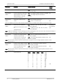
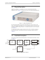
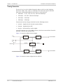
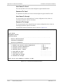
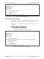
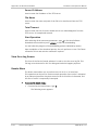
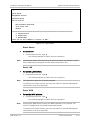
Figure 1-6. ASM-40 Clock Configuration
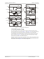
G.703-HDB3 Interface Timing
The received data from the analog side is output on the DTE interface with a
jitter-free clock for TC & RC (see Figure 1-7 and Figure 1-8). The transmit data on
the analog side is the input data from the DTE interface. The G.703-HDB3
recovered clock (from the input data) is used as an input clock for the transmit
FIFO, as shown in Figure 1-7. The same FIFO used for external clock is always
present when using the G.703-HDB3 interface).
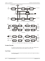
Using the internal or receive clock, provisions must be made to loop back (on the
DTE side) the incoming clock (data and clock out) to the transmit data (data and
clock inputs). Refer to Figure 1-8, for clock configuration.
ASM-40 Ver. 1.0
Functional Description
1-5