1
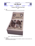
Marvell NanoLab
Member login
Lab Manual Contents
MercuryWeb
Berkeley Microlab
Chapter 8.8
CDE ResMap Four Point Probe
(cde-resmap - 380)
1.0
Title
CDE ResMap Four Point Probe Operation
2.0
Purpose
ResMap Four point Probe, made by Creative Design Engineering (CDE), is a semiautomatic tool to
measure the sheet resistance of a thin film or the bulk resistance of a wafer/sample. The
wafer/sample needs to get manually loaded onto the probe platform. Then the measurements are
automatically controlled according to the selected recipe that is pre-programmed. It is capable of
accommodating a wafer up to 12 inches in diameter. The maximum number of measurement sites
available is 99, and the measurement pattern can be circular, rectangular, linear along the diameter
of the wafer, or in a customized geometry. The measurement range is from 2 m Ω/□ to 5MΩ/□
with 0.5% accuracy.
3.0
Scope
This document covers the procedures of sheet resistance measurement, and the explanations
of the recipes.
4.0
Applicable Documents
ResMap Four Point Probe User Manual
Hard copy at the tool and soft copy stored in the PC.
5.0
6.0
Definitions & Process Terminology
5.1
Four Point Probe: A precision tool to measure the sheet resistance in a conductive media. The
probe has 4 pins in contact with the conductive sample. Two pins apply a current and the
voltage is measured across the other two pins. The sheet resistance can be calculated with the
current, voltage and the geometry of the sample.
5.2
Probe Configuration A: Current flows through two outer pins (1, 4) and voltage measured
across two inner pins (2, 3). This configuration has better signal to noise ratio.
5.3
Probe Configuration B: Current flows through pins (1, 3) and voltage measured across pins (2,
4). This configuration corrects for pin wobbling and can measure closer to sample edge.
Safety
Follow the general safety guidelines in the lab as well as the specific safety rules, as per follows:
6.1
Electric Shock: To prevent electric shock, do not change any switch settings and plug
connections.
CDE Resmap
7.0
Chapter 8.8
Statistical/Process Data
N/A
8.0
Available Processes, Process Notes
8.1
8.2
9.0
Available Programs:
8.1.1
4” Wafers: 49, 25, 9, 5, 1 point and 17 point diameter measurements.
8.1.2
6” wafers: 49, 25, 9, 5, 1 point and 25 point diameter measurements.
Process Notes:
8.2.1
The probe installed is type A: Tip radius 40 μm, Force 100grams, Tip spacing 1.0 mm.
8.2.2
To copy the measurement results, use Windows Screen Shot (Alt+PrintScreen). First
copy the screen display to the clipboard, and paste it to WordPad. Then you can use
USB flash memory drive to transfer the file to your PC.
Equipment Operation
9.1
Equipment Description
The Resmap Four Point Probe comprises of a probe station and a PC. Under the cover of the
probe station, there is a wafer stage with concentric circular grooves for aligning wafers from 2
to 12 inches. The maximum measurement diameter is 8”. On the out edge of the wafer stage,
there is a rectangular ceramic for probe pin conditioning. Do not touch the ceramic to avoid
contamination.
9.2
Measurement procedures
9.2.1
Enable the CDE ResMap Four Point Probe (cde-resmap).
9.2.2
Open the cover. Load and align your wafer/sample on the stage.
9.2.3
On the PC screen, click [Operator] drop down menu, then select [Run Recipe]. Select
the Recipe you plan to use from the appropriate project (section 11.1). Click [ok] button.
Or click [Previous] button to repeat the previous recipe.
9.2.4
The PC displays the Run Parameter screen. Enter the information on the left side of the
screen for record keeping purpose. Ignore the Wafer ID field on right side of the screen,
because the tool does not have a cassette loader.
9.2.5
Click the [Run] button and the tool run the selected recipe. When it finishes, the PC
displays the raw data of all the measurements.
once the measurements are completed, you can use the graphic utilities to
analyzie/organize your data.
remove your wafer, and log out of the machine. with the cover closed.
9.2.6
9.2.7
10.0
Trouble Shooting Guidelines
10.1 Problem:
Pins not touching sample.
-2-
CDE Resmap
Chapter 8.8
Cause:
Solution:
11.0
Measuring site is outside the sample. The sample may be misaligned or wrong
recipe selected.
Re-align sample; select correct recipe.
Figures And Schematics
11.1
Project and Recipe selection screen
11.2
Run Parameter screen.
-3-
CDE Resmap
Chapter 8.8
Note: All entries are for record keeping, no effect on measurements.
11.3
Sample Recipe screen (Engineer Menu)
-4-
CDE Resmap
Chapter 8.8
Note:
1.
2.
12.0
Conductor Thk for BULK field is used for BULK resistance measurement. It is not used for
SHEET resistance measurement.
ThOffset field is the angle (in degrees) that the entire measurement map to be rotated. If the
Randomize field is selected, the map will be rotated by a random amount less than ThOffset.
Appendices
12.1
Measuring the Film Thickness of a Metal Film
The thickness of a metal film cannot usually be measured optically like a dielectric
film because it is, in general, not transparent to light. The sheet resistance
measurement can be used to calculate film thickness. If one assumes the film
behaves like a bulk material (or the electrical and mechanical properties do not
change in the film within the thickness range), then one can express the thickness as,
t = ρ/Rs
where t, is the thickness, ρ is the bulk resistivity, and Rs is the sheet resistance. Many
films, however, do not behave nicely and ρ is not uniform within the thickness
-5-
CDE Resmap
Chapter 8.8
of the film. If we assume that ρ decreases as a function of thickness buildup (typical
within the first few hundred Å) then one can express the thickness (Å) as,
t = ρ´Rsβ
ρ´
FILM
Al
337.17
β
-0.92041
These values have been determined by SemiTech after much characterization.
-6-