1
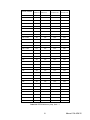
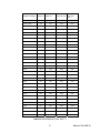
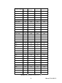
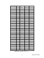
10623 Roselle Street, San Diego, CA 92121 y (858) 550-9559 y Fax (858) 550-7322
[email protected] y www.accesio.com
104-AIM-32
ANALOG INPUT SIGNAL CONDITIONER
USER MANUAL
FILE: M104-AIM-32-A1s
Notice
The information in this document is provided for reference only. ACCES does not assume any liability arising out
of the application or use of the information or products described herein. This document may contain or
reference information and products protected by copyrights or patents and does not convey any license under
the patent rights of ACCES, nor the rights of others.
IBM PC, PC/XT, and PC/AT are registered trademarks of the International Business Machines Corporation.
Printed in USA. Copyright 2003, 2005 by ACCES I/O Products, Inc. 10623 Roselle Street, San Diego, CA
92121. All rights reserved.
WARNING!!
ALWAYS CONNECT AND DISCONNECT YOUR FIELD CABLING WITH
THE COMPUTER POWER OFF. ALWAYS TURN COMPUTER POWER
OFF BEFORE INSTALLING A BOARD, CONNECTING AND
DISCONNECTING CABLES, OR INSTALLING BOARDS INTO A SYSTEM
WITH THE COMPUTER OR FIELD POWER ON MAY CAUSE DAMAGE TO
THE I/O BOARD AND WILL VOID ALL WARRANTIES, IMPLIED OR
EXPRESSED.
2
Manual 104-AIM-32
Warranty
Prior to shipment, ACCES equipment is thoroughly inspected and tested to applicable specifications. However,
should equipment failure occur, ACCES assures its customers that prompt service and support will be available.
All equipment originally manufactured by ACCES which is found to be defective will be repaired or replaced
subject to the following considerations.
Terms and Conditions
If a unit is suspected of failure, contact ACCES' Customer Service department. Be prepared to give the unit
model number, serial number, and a description of the failure symptom(s). We may suggest some simple tests
to confirm the failure. We will assign a Return Material Authorization (RMA) number which must appear on the
outer label of the return package. All units/components should be properly packed for handling and returned
with freight prepaid to the ACCES designated Service Center, and will be returned to the customer's/user's site
freight prepaid and invoiced.
Coverage
First Three Years: Returned unit/part will be repaired and/or replaced at ACCES option with no charge for labor
or parts not excluded by warranty. Warranty commences with equipment shipment.
Following Years: Throughout your equipment's lifetime, ACCES stands ready to provide on-site or in-plant
service at reasonable rates similar to those of other manufacturers in the industry.
Equipment Not Manufactured by ACCES
Equipment provided but not manufactured by ACCES is warranted and will be repaired according to the terms
and conditions of the respective equipment manufacturer's warranty.
General
Under this Warranty, liability of ACCES is limited to replacing, repairing or issuing credit (at ACCES discretion)
for any products which are proved to be defective during the warranty period. In no case is ACCES liable for
consequential or special damage arriving from use or misuse of our product. The customer is responsible for all
charges caused by modifications or additions to ACCES equipment not approved in writing by ACCES or, if in
ACCES opinion the equipment has been subjected to abnormal use. "Abnormal use" for purposes of this
warranty is defined as any use to which the equipment is exposed other than that use specified or intended as
evidenced by purchase or sales representation. Other than the above, no other warranty, expressed or implied,
shall apply to any and all such equipment furnished or sold by ACCES.
3
Manual 104-AIM-32
Table of Contents
Chapter 1: Introduction ......................................................................................................... 5
Specification...................................................................................................................................................... 7
Figure 1-1: Block Diagram............................................................................................................................. 8
Chapter 2: Installation........................................................................................................... 9
Figure 2-1: PC/104 Key Information ............................................................................................................ 10
Chapter 3: Option Selection ............................................................................................... 11
Figure 3-1: Option Selection Map................................................................................................................ 11
Chapter 4: Address Selection............................................................................................. 12
Table 4-1: Standard Address Assignments for Standard Computers.......................................................... 12
Chapter 5: Programming .................................................................................................... 13
Table 5-1: Register Map .............................................................................................................................. 13
Table 5-2: Range Selection ......................................................................................................................... 13
Factory-Installed Options............................................................................................................................... 15
Figure 5-1: Standard Voltage Input Configuration....................................................................................... 15
Figure 5-2: Voltage Input With Attenuator ................................................................................................... 15
Figure 5-3: Current Input Configuration....................................................................................................... 15
Figure 5-4: Thermocouple Input Configuration............................................................................................ 16
Figure 5-5: RTD Input Configuration ........................................................................................................... 16
Figure 5-6: Bridge Completion Configuration .............................................................................................. 16
Chapter 6: Connector Pin Assignments............................................................................ 17
Table 6-1: Connector P2, Single-Ended Inputs ........................................................................................... 17
Table 6-2: Connector P2, Differential Inputs................................................................................................ 18
Table 6-3: Connector P3, Outputs ............................................................................................................... 19
Chapter 7: Calibration and Test ......................................................................................... 20
Appendix A: Calibration...................................................................................................... 21
System Calibration ......................................................................................................................................... 21
Table A-1: Range Selection......................................................................................................................... 21
Internal Calibration Procedure ...................................................................................................................... 22
Appendix B: EEPROM Calibration Addresses .................................................................. 25
Table B-1: EEPROM Memory Map, Gain = 0.5........................................................................................... 25
Table B-2: EEPROM Memory Map, Gain = 1.............................................................................................. 26
Table B-3: EEPROM Memory Map, Gain = 2.............................................................................................. 27
Table B-4: EEPROM Memory Map, Gain = 50............................................................................................ 28
Table B-5: EEPROM Memory Map, Gain = 100.......................................................................................... 29
Table B-6: EEPROM Memory Map, Gain = 200.......................................................................................... 30
4
Manual 104-AIM-32
Chapter 1: Introduction
Standard Features
•
Designed to pair with an A/D board to increase channel count and signal conditioning
capabilities
•
32 single-ended or 16 differential inputs
•
6 software-programmable ranges:
±25mV, ±50mV, ±0.1V, ±2.5V, ±5V, ±10V (analog input
ranges can be mixed, any channel may have any range at any time)
•
Up to 7 104-AIM-32s can be stacked per A/D board for up to 224 S.E. or 112 diff. Inputs
•
+5VDC-only operation
•
15VDC sensor excitation
•
Input signal conditioning
•
Full system calibration including sensor and A/D board
•
Individual offset and gain factors for each channel and gain
Factory Options
•
4-20mA inputs
•
RTD & thermocouple measurement
•
Voltage divider on each input
•
RC filters on each input
•
Bridge completion configuration
•
0 to 70°C and -40 to +85°C versions available
•
TC break detect
Description
This board is an analog signal conditioner/multiplexer. Any one of 16 differential or 32 single-ended analog
signals may be selected via a software command. The multiplexer’s high impedance along with the signal
conditioning front end provides an interface to multiple sensors without compromising the quality of the gathered
data.
An optional screw terminal block is available for the termination of the input signals, which can come from a
variety of sensors: thermocouples (J,K,T,E,S,R, and B), three-wire RTD's (both 392- and 385-alpha), strain
gages, 4-20mA current inputs as well as DC and AC voltage inputs. Provision for installation of bridge
completion resistors, current sensing resistors and for resistors in series with RTDs are provided as well as a
15VDC source for bridge and RTD excitation (see the Factory-Installed Options section).
To provide a reference junction compensation for the thermocouples, a two-wire temperature sensor should be
installed on the input terminal block. The eighth output channel is dedicated to this temperature measurement.
The signal selected by the input multiplexer is filtered (RC, low pass) and amplified. After the conditioning, the
signal can be jumpered to one of seven output channels.
5
Manual 104-AIM-32
While any A/D converter that will accept inputs in common voltage ranges (0-5V, +5V) is compatible, this board
output is designed to connect to a 12-8-type Analog to Digital board.
Mixed-range analog inputs are conveniently managed with the extensive programming flexibility of the board.
Six dynamically software-programmable gains, each with automatic offset compensation and gain correction,
allow the system to utilize the full resolution of the A/D converter.
The offset and gain correction coefficients for up to 32 analog channels (times the 6 voltage ranges that may be
selected for each channel) are available. Software tools are provided for the user to ‘null out’ input voltage
offsets and adjust gain for all channels.
The board may be used as part of a large data acquisition system. A system may comprise one to seven of
these boards per Analog to Digital Converter board. An on-board DC-DC converter which operates from the
+5VDC computer power supply provides +15VDC for the board’s circuitry, and also the regulated excitation
voltage.
The board occupies eight bytes of I/O address space. The base address is selectable via jumpers anywhere
within the range of 0-3F8 hex (mapped only into the first 1K of I/O space, compatible with PC/104-Plus
addressing). An illustrated setup program is provided, interactive displays show locations and proper settings of
jumpers. Also, sample programs in several languages are provided on CD and are described in the
Programming section of this manual.
6
Manual 104-AIM-32
Specification
Analog Inputs
•
Channels:
16 Differential or 32 Single-ended.
•
ESD Protection
Greater than 2000V.
•
Input Impedance:
5M Ohms Differential, 10M Ohms Single-ended.
•
Common Mode Voltage:+13V.
•
Maximum Input Voltage:250V with voltage divider, 40V without voltage divider
•
Current Loop:
4-20mA with on-board attenuator installed, factory option.
•
Voltage Ranges:
±10V, ±5V, ±2.5V, ±100mV, ±50mV, ±25mV. Selectable per channel
Analog Outputs
•
Channels:
1 of 8, jumper selected (8th channel is temp sensor output if used)
•
•
Output Drive:
Output Voltage:
10mA
+5V with a full scale input (+12V rails).
General
•
Operating Temperature: 0 to 70°C, -40 to +85°C optional, all options.
•
Storage Temperature:
-55 to +125°C.
•
Humidity:
5% to 95% RH, non-condensing.
•
Power Required:
+5V @ 200mA with no load on excitation.
•
Temp. Sensor:
+10mV / °K @ 25°C. Output voltage temperature coefficient
7
Manual 104-AIM-32
Figure 1-1: Block Diagram
8
Manual 104-AIM-32
Chapter 2: Installation
A printed Quick-Start Guide (QSG) is packed with the board for your convenience. If you’ve already performed
the steps from the QSG, you may find this chapter to be redundant and may skip forward to begin developing
your application.
The software provided with this PC/104 Board is on CD and must be installed onto your hard disk prior to use.
To do this, perform the following steps as appropriate for your operating system. Substitute the appropriate drive
letter for your CD-ROM where you see d: in the examples below.
CD Installation
The following instructions assume the CD-ROM drive is drive “D”. Please substitute the appropriate drive letter
for your system as necessary.
DOS
1.
Place the CD into your CD-ROM drive.
2.
Type B- to change the active drive to the CD-ROM drive.
3.
4.
Type GLQR?JJ- to run the install program.
Follow the on-screen prompts to install the software for this board.
WINDOWS
1.
Place the CD into your CD-ROM drive.
2.
The system should automatically run the install program. If the install program does not run
promptly, click START | RUN and type BGLQR?JJ, click OK or press -.
3.
Follow the on-screen prompts to install the software for this board.
LINUX
1.
Please refer to linux.htm on the CD-ROM for information on installing under linux.
9
Manual 104-AIM-32
Installing the Hardware
Before installing the board, carefully read Chapter 3 and Chapter 4 of this manual and configure the board
according to your requirements. The SETUP Program can be used to assist in configuring jumpers on the
board. Be especially careful with Address Selection. If the addresses of two installed functions overlap, you will
experience unpredictable computer behavior. To help avoid this problem, refer to the FINDBASE.EXE program
installed from the CD. The setup program does not set the options on the board, these must be set by jumpers.
To Install the Board
1.
Install jumpers for selected options and base address according to your application requirements, as
mentioned above.
2.
Remove power from the PC/104 stack.
3.
Assemble standoff hardware for stacking and securing the boards.
4.
Carefully plug the board onto the PC/104 connector on the CPU or onto the stack, ensuring proper
alignment of the pins before completely seating the connectors together.
5.
Install I/O cables onto the board’s I/O connectors and proceed to secure the stack together or repeat
steps 3-5 until all boards are installed using the selected mounting hardware.
6.
Check that all connections in your PC/104 stack are correct and secure then power up the system.
7.
Run one of the provided sample programs appropriate for your operating system that was installed from
the CD to test and validate your installation.
Figure 2-1: PC/104 Key Information
10
Manual 104-AIM-32
Chapter 3: Option Selection
P3
Choose one output
“channel” for the
conditioned signal
CH1
CH0
CH3
CH2
Pin 1
CH5
CH4
Install for LM135
T-Couple CJC only
CH7
CH6
The board’s base address, output channel, and temp sensor output are the only jumper selectable options.
Voltage input ranges are selected via software. Special signal conditioning for different input types are factory
installed options.
JUMPER
CH0
CH1
CH2
CH3
CH4
CH5
CH6
ADDRESS 0x340
A9
A8
A7
A6
A5
A4
A3
PIN
P3-6
P3-8
P3-14
P3-16
P3-22
P3-24
P3-30
P2
Pin 1
Figure 3-1: Option Selection Map
Adding cold junction compensation when using thermocouples
Connect an LM335 Precision Temperature Sensor lead 2 (cathode) to P2-25 (Temperature Sensor) and put the
LM335 pin 3 (anode) to GND (P2-24 or P2-26 are the nearest physical ground pins on the connector). Leave the
LM335 lead 1 not connected (NC). Install a jumper at position CH7 on the board, which routes the Temperature
Sensor to the output connector pins for channel 7 (P3-33). Using the AI12-8 and a ribbon cable that has a one
to one connection reading CH7 on the A/D board would give the user the CJC value. Otherwise you could route
channel 7 output of the AIM-32 to any of your A/D inputs and read that channel for the CJC value.
Note: There is a 2.7K ohm bias resistor ( R17 ) from VCC ( +5V ) to P2-25 ( TEMP ) on the board.
11
Manual 104-AIM-32
Chapter 4: Address Selection
The board occupies 8 bytes of I/O space. The board base address can be selected anywhere within the I/O
address range 0-3F8 hex. If in doubt of where to assign the base address, refer to the following tables and the
FINDBASE program to find an available address for your system.
HexRange
Usage
000-00F
020-021
040-043
060-06F
070-07F
080-09F
0A0-0BF
0C0-0DF
0F0-0F1
0F8-0FF
170-177
1F0-1F8
200-207
238-23B
23C-23F
278-27F
2B0-2BF
2C0-2CF
2D0-2DF
2E0-2E7
2E8-2EF
2F8-2FF
300-30F
310-31F
320-32F
370-377
378-37F
380-38F
3A0-3AF
3B0-3BB
3BC-3BF
3C0-3CF
3D0-3DF
3E8-3EF
3F0-3F7
3F8-3FF
DMA Controller 1
INT Controller 1, Master
Programmable Interrupt Timer
Keyboard Controller
Real Time Clock, NMI Mask
DMA Page Register
INT Controller 2
DMA Controller 2
Math Coprocessor
Math Coprocessor
Fixed Disk #1
Fixed Disk #2
Game I/O
Bus Mouse
Alt. Bus Mouse
Parallel Printer
EGA
EGA
EGA
GPIB (AT)
Serial Port
Serial Port
Prototype Board
Prototype Board
Hard Disk (XT)
Floppy Controller #2
Parallel Printer Port 1
SDLC
SDLC
Monochrome Display/Printer
Parallel Printer Port 2
VGA EGA
CGA
Serial Port
Floppy Diskette Controller
Serial Port
Table 4-1: Standard Address Assignments for Standard Computers
To set the desired board address, jumpers must be installed on the board. These jumpers are marked
A5-A9 and form a binary representation of the address in negative-true logic. (assign '0' to all Address
Setup jumpers installed, and assign '1' to all Address Setup jumpers left off.)
Base Address Table
To set the base address of the board, install the jumpers “ON” the posts for that address according to the table.
12
Manual 104-AIM-32
Chapter 5: Programming
Address
Port Assignment
Operation
Base Address
Command Register
Read / Write
Base Address +1
Setup Register
Read / Write
Base Address +2
EEPROM Address, LSB
Read / Write
Base Address +3
EEPROM Address, MSB
Read / Write
Base Address +4
EEPROM I/O Register
Read / Write
Table 5-1: Register Map
The purpose of this board is to select an input signal, condition it (filter ,attenuate, amplify) and present the
result on output pins. This output is usually applied to an analog to digital converter. To accomplish this, three
things must happen: the input must be identified as either singled-ended or differential, the pin or pins to which
the signal is applied must be identified, and the gain to be applied to the signal must be selected. The Command
Register and bit 0 of the Setup Register are used to supply this information to the board.
Gain and offset calibration data can be stored for the board alone or for the entire system (i.e. for sensors and
an analog to digital converter board as well).
Base + 0: Command Register
Bit 7
Bit 6
Bit 5
Voltage
Voltage
Voltage
Range Select Range Select Range Select
Bit 0
Bit 1
Bit 2
Bit 4
Bit 3
Bit 2
Bit 1
Bit 0
Channel
Select
Bit 4
Channel
Select
Bit 3
Channel
Select
Bit 2
Channel
Select
Bit 1
Channel
Select
Bit 0
This register specifies which input channel the multiplexer routes to the amplifier circuit (bits 0 through 4) and to
specify the gain (also called 'range') of the amplifier (bits 5 through 7). Writing to this register will update the
multiplexer channel and will load calibration data appropriate to the channel and gain settings from the
EEPROM to the digital potentiometers that modify the DC offset and gain of the amplifier. Note that the gain
settings may be different for each channel. If Cal Data Enable(bit 4 of the Setup Register) is LOW, the EEPROM
will be ignored and the pots will be fixed at mid-range.
At gains of 50, 100, or 200, the switching “glitches” of the multiplexers will be amplified to the extent that they
appear as noise at the output. A delay of approximately 35 microseconds is recommended before the output of
the board is used at one of the higher gains.
Bit 7, Bit 6, Bit 5
Voltage Range
Gain
000
±10
0.5
001
±5
1.0
010
±2.5
2.0
011
±100mV
50
100
±50mV
100
101
±25mV
200
Table 5-2: Range Selection
13
Manual 104-AIM-32
Base + 1: Setup Register
Bit 7
Bit 6
Bit 5
Bit 4
Bit 3
Bit 2
Bit 1
Bit 0
EEPROM
Busy
(read)
Digital Pots
Busy
(read)
Reserved
Cal. Data
Enable
Cal. Data
Space
Source
Gnd / Vref
Internal Cal.
Source
SE / Diff.
This register contains various setup-oriented bits:
•
•
•
•
•
•
•
SE / Diff (bit 0) identifies the input signal as either single-ended (HIGH) or differential (LOW).
Cal Data Enable (bit 4) enables (if HIGH) or disables (if LOW) the loading of calibration constants from
the EEPROM.
Cal Data Space (bit 3) selects which of two EEPROM spaces calibration constants are taken from,
factory calibration (HIGH) or user calibration (LOW).
When Internal Cal Source (bit 1) is HIGH, the board ignores its normal inputs, instead using one of two
voltage sources provided internally for calibrating the board.
Source Gnd / Vref ( bit 2) selects between these internal voltage sources. When LOW, 0V will be
provided internally (for offset calibration), and when HIGH, 4.096V will be provided internally (for gain
calibration).
The Digital Pots Busy bit indicates that offset and gain calibration data is being moved from the
EEPROM to the digital potentiometers. This happens each time that a byte is written to the COMMAND
register and takes about 3uS.
EEPROM Busy (bit 7) is HIGH when the EEPROM is being accessed. While busy, any further EEPROM
accesses will be ignored or return garbage data.
On power-up all control bits are LOW, the factory calibration space is selected (as explained in the Calibration
section), the internal calibration source is disconnected, and inputs are differential.
Base + 2 & Base + 3: EEPROM Address Register (read/write)
To read from or write to the EEPROM, first write the 11-bit address of the byte within the EEPROM to this wordwide register. The address bytes can also be written separately to Base + 2 and Base + 3, for example on an 8bit PC/104 bus. After setting the address, read or write data via the EEPROM I/O Register at Base + 4. Use the
EEPROM Busy bit (in the Setup Register at Base + 1) to tell when the EEPROM is ready to be accessed again.
The EEPROM address corresponding to each calibration constant is shown in Appendix B: EEPROM
Calibration Addresses.
Base + 4: EEPROM I/O Register
This register is used to read data from or write data to the EEPROM once the address has been set in the
EEPROM Address Register at Base + 2. A READ reads the byte and a WRITE writes over it. Use the EEPROM
Busy bit (bit 7 in the Setup Register at Base + 1) to tell when the EEPROM is ready to be accessed again.
14
Manual 104-AIM-32
Factory-Installed Options
Each channel can have one of the following configurations.
Standard Configuration. An RC filter is installed on the input of each channel (Fig. 5-1). The user may specify
the filter’s capacitance for each channel. 1K ohms and 100pF are standard.
Figure 5-1: Standard Voltage Input Configuration
Input Voltage Divider. The standard model configuration is intended for voltage inputs of no more than +10V,
while this input option allows voltages higher than +10V. Resistive voltage dividers are installed on channels
specified by the user ( Fig. 5-2).
Figure 5-2: Voltage Input With Attenuator
4-20mA Current Input. Precision resistors are installed from the positive input to the negative input of all
differential channels. (Fig. 5-3). The input is not offset, so that a 4-20mA input will be read as 1 to 5V. Readings
below 4mA will read between 0 and 1V (providing fault detection, i.e. for a blown circuit fuse).
Figure 5-3: Current Input Configuration
Thermocouple Measurement with reference junction temperature sensor. The temperature sensor is
located at terminal block positions 25 and 26, and its output is connected to the Channel 7 output jumper. If
more than one board is used, a reference junction sensor can be connected on an S.E. voltage input channel.
This would also allow for complete sensor calibration.
15
Manual 104-AIM-32
Thermocouple Break Detect. Break-detect resistors may be installed. With this feature an open thermocouple
condition will cause a full-scale negative voltage output. Break-detect resistors are installed between each
channel’s positive input and +15V and between each channel’s negative input and ground (Fig. 5-4).
Figure 5-4: Thermocouple Input Configuration
RTD Measurement. The RTD option accommodates three-wire RTD's (Fig. 5-5). A 66.5KOhm precision resistor
in series with an RTD lead wire and the RTD sensor determines the sensor supply current. The 66.5KOhm
resistor is connected between the +15V supply and ground through the 2nd lead wire to provide lead length
compensation. The voltage drops across the lead wires cancel at the differential signal input.
Figure 5-5: RTD Input Configuration
Bridge Completion Configuration. Three resistors are installed so as to form 3-arms of a full Wheatstone
bridge. The resistor values are specified by the customer ( Fig. 5-6).
Figure 5-6: Bridge Completion Configuration
16
Manual 104-AIM-32
Chapter 6: Connector Pin Assignments
Pin #
Signal Name
Pin #
Signal
Name
1
CH00
26
GROUND
2
CH16
27
CH08
3
GROUND
28
CH24
4
CH01
29
GROUND
5
CH17
30
CH09
6
GROUND
31
CH25
7
CH02
32
GROUND
8
CH18
33
CH10
9
GROUND
34
CH26
10
CH03
35
GROUND
11
CH19
36
CH11
12
GROUND
37
CH27
13
CH04
38
GROUND
14
CH20
39
CH12
15
GROUND
40
CH28
16
CH05
41
GROUND
17
CH21
42
CH13
18
GROUND
43
CH29
19
CH06
44
GROUND
20
CH22
45
CH14
21
GROUND
46
CH30
22
CH07
47
GROUND
23
CH23
48
CH15
24
GROUND
49
CH31
25
TEMPERATURE
SENSOR
50
GROUND
Table 6-1: Connector P2, Single-Ended Inputs
17
Manual 104-AIM-32
Pin #
Signal Name
Pin #
Signal
Name
1
CH00+
26
GROUND
2
CH00 -
27
CH08+
3
GROUND
28
CH08+
4
CH01+
29
GROUND
5
CH01 -
30
CH09+
6
GROUND
31
CH09 -
7
CH02+
32
GROUND
8
CH02 -
33
CH10+
9
GROUND
34
CH10 -
10
CH03+
35
GROUND
11
CH03 -
36
CH11+
12
GROUND
37
CH11 -
13
CH04+
38
GROUND
14
CH04 -
39
CH12+
15
GROUND
40
CH12 -
16
CH05+
41
GROUND
17
CH05 -
42
CH13+
18
GROUND
43
CH13 -
19
CH06+
44
GROUND
20
CH06 -
45
CH14+
21
GROUND
46
CH14 -
22
CH07+
47
GROUND
23
CH07 -
48
CH15+
24
GROUND
49
CH15 -
25
TEMPERATURE
SENSOR
50
GROUND
Table 6-2: Connector P2, Differential Inputs
18
Manual 104-AIM-32
Pin #
Signal Name
Pin #
Signal Name
1
no connection
18
no connection
2
no connection
19
GROUND
3
GROUND
20
no connection
4
no connection
21
no connection
5
no connection
22
CHANNEL 4
6
CHANNEL 0
23
GROUND
7
GROUND
24
CHANNEL 5
8
CHANNEL 1
26
no connection
9
no connection
27
GROUND
10
no connection
28
no connection
11
GROUND
29
no connection
12
no connection
30
CHANNEL 6
13
no connection
31
GROUND
14
CHANNEL 2
32
CHANNEL 7
15
GROUND
33
GROUND
16
CHANNEL 3
34
no connection
Table 6-3: Connector P3, Outputs
19
Manual 104-AIM-32
Chapter 7: Calibration and Test
All boards may be calibrated prior to shipment at the user’s request. Periodic calibration of this board is
recommended. The calibration interval depends to a large extent on the board’s environment. For environments
where there are frequent large changes of temperature and/or vibration, a three-month interval is suggested.
For laboratory or office conditions, six months to a year is acceptable.
A multi-meter that can measure a voltage change as low as 780uV is required to accurately calibrate the board.
Also, a voltage calibrator or a stable, noise-free, DC voltage source that can be used in conjunction with the
digital multi-meter is required for best results.
Calibration may be performed using one of the programs supplied with the board. This software will lead the
user through the set up and calibration procedure with prompts and graphic displays.
The board’s signal-conditioning circuit (that part which amplifies, attenuates, or level-shifts) may be calibrated
independently. Six bytes (one per voltage range) for offsets and six bytes for gain adjustments are stored in the
board’s EEPROM for each input (16 diff. or 32 S.E.). If the user has a 12-8-type Analog to Digital Converter
board, software is provided that will automate this internal calibration. Run the calibration program and follow the
prompts.
The board comes with a calibration program that, in conjunction with current or voltage sources and meters and
user interaction, will calibrate the system. Voltage offsets at the board’s input pins plus any offset generated on
the board plus offset from the A/DC can be nulled out. Gain adjustment of +5% can be saved in the EEPROM
for each input (up to 32 signals) times each voltage range.
20
Manual 104-AIM-32
Appendix A: Calibration
System Calibration
The board accepts a mix of differential and single-ended inputs. There is a specific location in the board’s
EEPROM for each signal’s offset adjustment and gain adjustment. For example, assume that a differential
signal is connected to P2 pins 1 and 2. The DC offset and gain adjust values should be written to the board’s
EEPROM at 0h and 100h for the ±10V range, at 20h and 120h for the ±5V range, etc. Refer to the EEPROM
memory map to identify the locations required.
Overview
These are the steps we recommend to null the offsets. Fill the user’s section of the EEPROM with the digital
pot’s center value. Turn off the switch that applies an internal reference and turn on the calibration system.
Connect the system’s voltages that are to be monitored to the inputs at connector P2 and cause them to be 0V.
Select an input channel (0 through 31 single-ended or 0 through 15 differential) and a voltage range (gain may
be .5, 1, 2, 50, 100, or 200). Assuming that the output of the system is an A/DC, select an output pin at
connector P3 (place a jumper on the appropriate pins, see the Option Selection map) and trigger a conversion.
Iteratively modify the value in the EEPROM, update the value in the digital pot that controls the offset, and
measure the output. The target output voltage is equal to the input voltage. Do this for each range.
These are the steps we recommend to adjust the gains. Turn off the switch that applies an internal reference
and turn on the calibration system. Connect the system’s voltages that are to be monitored to the board’s inputs
at connector P2 and cause them to be at their maximum. Select an input channel (0 through 31 single-ended or
0 through 15 differential) and the appropriate range (±25mV, ±50mV, ±100mV, ±2.5V, ±5V, ±10V). Assuming
that the output of the system is an A/DC, select an output pin at connector P3 (place a jumper on the
appropriate pins, see the Option Selection map) and trigger a conversion. Iteratively modify the value in the
EEPROM, update the value in the digital pot that controls the offset, and measure the output. The target output
voltage is equal to the input voltage. Do this for each input channel.
Procedures
1.
If possible, set the output of a signal to be measured to 0V.
2.
Write 10h to the Setup register if the signal channel to be calibrated is differential. Write 11h for singleended signals.
Bit 7, Bit 6, Bit 5
Voltage Range
Gain
000
±10
0.5
001
±5
1.0
010
±2.5
2.0
011
±100mV
50
100
±50mV
100
101
±25mV
200
Table A-1: Range Selection
3.
Write 80h to the EEPROM at the offset adjust and gain adjust addresses for the signal channel to be
calibrated. The EEPROM requires approximately 1mS to store a byte, a ‘busy’ bit is set in the Setup byte
while this happens (bit 7).
21
Manual 104-AIM-32
4.
The Command register has two fields: the channel number (bits 0 through 4) and the range selection. For
the signal channel to be calibrated, write the combined range and channel to the Command register. The
board will retrieve calibration data from the EEPROM and load it in the digital pots each time a byte is
written to the Command register.
5.
If possible, use the A/DC connected to the output of the board to digitize the voltage. As in the internal
calibration of the board, adjust the calibration value to compensate for any DC offset.
6.
If possible, set the voltage of the signal to a value near the top of its range. Trigger a conversion and, as in
the internal calibration, adjust the value in the EEPROM up or down until the output of the system is
correct.
7.
Repeat these steps for all of the channels in use.
Internal Calibration Procedure
The following steps are suggested methods for nulling the offsets and calibrating the gains of the
instrumentation amplifier chain at it’s six ranges. Note that only the lower gain settings can be calibrated
internally, the input is fixed at the 4.096V reference and the output is limited to ± 12V.
The EEPROM memory stores calibration data in 24 blocks. Each gain setting has a block for the user’s offset
adjust, the user’s gain adjust, the factory offset adjust, and the factory gain adjust (ie., 4 major blocks times 6
gains).
Overview
These are the steps we recommend to null the offsets (see paragraphs 1 through 11). Fill the user’s section of
the EEPROM with the digital pot’s center value. Using a meter or ‘scope or A/DC, monitor the output at
connector P3 relative to the board’s ground (P3 pin 3). Connect Ground to the board’s instrumentation amplifier
through an internal switch and turn on the calibration system. Select a voltage range (gain may be .5, 1, 2, 50,
100, or 200). Iteratively modify the value in the EEPROM, update the value in the digital pot that controls the
offset, and measure the output. The target output voltage is 0V. Do this for each range.
Procedure
1.
Write 80h to the first 1C0h EEPROM locations. Gain and offsets can be adjusted positive or negative, 80h
is the midpoint (close to zero effect).
a.
A byte in the EEPROM is addressed by writing an eleven-bit pointer to a word-wide register at the
board’s base address plus 2 (i.e., if the board’s address = 300h then this register is at 302h). Write
0h to this word-wide register.
b.
Write 80h to the EEPROM I/O address (base + 4), the value will be stored in the EEPROM. The
Busy flag, bit 7 of the Setup register, will go HIGH for 1mS.
c.
When the Busy flag is LOW, increment the EEPROM address and repeat step B. Do this until the
first 1C0h EEPROM bytes = 80h. Note that the EEPROM can be read in the same manner (load the
address pointer, read base+6) as quickly as a read can be issued.
2.
Connect a meter between the board’s output and the board’s GROUND.
3.
Write 13h to the Setup register. This will connect Ground to the board’s instrumentation amplifier input and
allow calibration data to be copied from the EEPROM to the digital pots.
4.
Write 0h to the Command register. This will select the ±10V range, gain = 0.5.
5.
Null the output offset for the ±10V range by changing the calibration data in the EEPROM.
22
Manual 104-AIM-32
a.
If the meter reads a positive voltage, write a value that's less than 80h to EEPROM addresses 0
through 1Fh (initialize the pointer at base+2 (LSB) and base+3 (MSB), write the value to base+4,
increment the pointer, write the value, etc.).
b.
Write 0h to the Command register. This will update the digital pots.
c.
If the meter reads positive, decrement the value in the EEPROM. If the meter reads negative,
increment the value and repeat step b.
Repeat as needed until the output is close to zero.
6.
Write 20h to the Command register. This will select the +5V range, gain = 1.
7.
Null the output offset for the ±5V range by changing the calibration data in the EEPROM.
a.
If the meter reads a positive voltage, write a value that's less than 80h to EEPROM addresses 20h
through 3Fh.
b.
Write 20h to the Command register. This will update the digital pots.
c.
If the meter reads positive, decrement the value in the EEPROM and repeat step b. If the meter
reads negative, increment the value and repeat step b.
Repeat as needed until the output is close to zero.
8.
Null the offset for the ±2.5V range (gain = 2). The value written to the command register is 40h. The
EEPROM address block is 40h to 5Fh.
9.
Null the offset for the ±0.1V range (gain = 50). The value written to the command register is 60h. The
EEPROM address block is 60h to 7Fh.
10.
Null the offset for the ±0.05V range (gain = 100). The value written to the command register is 80h. The
EEPROM address block is 80h to 9Fh.
11.
Null the offset for the ±0.025V range (gain = 200). The value written to the command register is A0h. The
EEPROM address block is A0h to BFh.
These are the steps we recommend to adjust the gain (see paragraphs 12 through 18). Using a meter or ‘scope
or A/DC, monitor the output at connector P3 relative to the board’s ground (P3 pin 3). Connect 4.096V to the
instrumentation amplifier through an internal switch and turn on the calibration system. Select a voltage range
(gain may be .5, 1, or 2). Iteratively modify the value in the EEPROM, update the value in the digital pot that
controls the gain, and measure the output. The target output voltages are 2.048V (gain = .5), 4.096V (gain = 1),
and 8.192V (gain = 2). Do this for the three lowest ranges, the higher ranges will be off-scale.
12.
Write 17h to the Setup register (enable calibration data, connect 4.096V to the gain stage, select single
ended inputs). Connect the negative meter probe to P3 pin 3 and the positive probe to the board's output.
Alternatively, connect a AIO12-8 (or an AI12-8) to P3, trigger a conversion, and read the value.
13.
Write 0h to the Command register. This will set the gain to 0.5 (+10V range) and cause the calibration
value to be copied from the EEPROM to the digital potentiometer. Ideally, the meter should read 2.048V.
14.
Adjust the gain for the ±10V range by changing the calibration data in the EEPROM.
a.
If the meter reads more than 2.048V, write a value that's less than 80h to EEPROM addresses 100h
through 11Fh (initialize the pointer at base+2 (LSB) and base+3 (MSB), write the value to base+4,
increment the pointer, write the value, etc.).
b.
Write 0h to the Command register. This will update the digital pots.
c.
If the meter reads HIGH, decrement the value in the EEPROM and repeat step b. If the meter reads
LOW, increment the value and repeat step b. If the meter reads as close as it’s going to get then
write the value to the EEPROM locations.
Repeat as needed until the output is close to 2.048V.
15.
Write 20h to the Command register. This will select the +5V range, gain = 1.
16.
Adjust the gain for the ±5V range by changing the calibration data in the EEPROM.
23
Manual 104-AIM-32
a.
If the meter reads more than 4.096V, write a value that's less than 80h to EEPROM addresses 120h
through 13Fh.
b.
Write 20h to the Command register. This will update the digital pots.
c.
If the meter reads HIGH, decrement the value in the EEPROM and repeat step b. If the meter reads
LOW, increment the value and repeat step b. If the meter reads as close as it’s going to get then
write the value to the EEPROM locations.
Repeat as needed until the output is close to 4.096V.
17.
Write 40h to the Command register. This will select the ±2.5V range, gain = 2.
18.
Adjust the gain for the ±2.5V range by changing the calibration data in the EEPROM.
a.
If the meter reads more than 8.192V, write a value that's less than 80h to EEPROM addresses 140h
through 15Fh.
b.
Write 40h to the Command register. This will update the digital pots.
c.
If the meter reads HIGH, decrement the value in the EEPROM and repeat step b. If the meter reads
LOW, increment the value and repeat step b. If the meter reads as close as it’s going to get then
write the value to the EEPROM locations.
Repeat as needed until the output is close to 8.192V.
The gain error of the ±100mV range (gain = 50), the ±0.05V range (gain = 100), and the ±0.025V range (gain =
200) cannot be calibrated out using the internal reference, the outputs are limited to ~12V. Optionally, these
ranges may be calibrated at the factory (using the ‘system calibration’ method).
24
Manual 104-AIM-32
Appendix B: EEPROM Calibration Addresses
OFFSET,
USER CAL
GAIN ADJUST,
USER CAL
OFFSET,
FACTORY CAL
GAIN ADJUST,
FACTORY CAL
00 SE / 00 Diff.
00h
100h
200h
300h
01 SE / 01 Diff.
01h
101h
201h
301h
02 SE / 02 Diff.
02h
102h
202h
302h
03 SE / 03 Diff.
03h
103h
203h
303h
04 SE / 04 Diff.
04h
104h
204h
304h
05 SE / 05 Diff.
05h
105h
205h
305h
06 SE / 06 Diff.
06h
106h
206h
306h
07 SE / 07 Diff.
07h
107h
207h
307h
08 SE / 08 Diff.
08h
108h
208h
308h
09 SE / 09 Diff.
09h
109h
209h
309h
10 SE / 10 Diff.
0Ah
10Ah
20Ah
30Ah
11 SE / 11 Diff.
0Bh
10Bh
20Bh
30Bh
12 SE / 12 Diff.
0Ch
10Ch
20Ch
30Ch
13 SE / 13 Diff.
0Dh
10Dh
20Dh
30Dh
14 SE / 14 Diff.
0Eh
10Eh
20Eh
30Eh
15 SE / 15 Diff.
0Fh
10Fh
20Fh
30Fh
16 SE
10h
110h
210h
310h
17 SE
11h
111h
211h
311h
18 SE
12h
112h
212h
312h
19 SE
13h
113h
213h
313h
20 SE
14h
114h
214h
314h
21 SE
15h
115h
215h
315h
22 SE
16h
116h
216h
316h
23 SE
17h
117h
217h
317h
24 SE
18h
118h
218h
318h
25 SE
19h
119h
219h
319h
26 SE
1Ah
11Ah
21Ah
31Ah
27 SE
1Bh
11Bh
21Bh
31Bh
28 SE
1Ch
11Ch
21Ch
31Ch
29 SE
1Dh
11Dh
21Dh
31Dh
30 SE
1Eh
11Eh
21Eh
31Eh
31 SE
1Fh
11Fh
21Fh
31Fh
CHANNEL NUMBER
Table B-1: EEPROM Memory Map, Gain = 0.5
25
Manual 104-AIM-32
OFFSET,
USER CAL
GAIN ADJUST,
USER CAL
OFFSET,
FACTORY CAL
GAIN ADJUST,
FACTORY CAL
00 SE / 00 Diff.
20h
120h
220h
320h
01 SE / 01 Diff.
21h
121h
221h
321h
02 SE / 02 Diff.
22h
122h
222h
322h
03 SE / 03 Diff.
23h
123h
223h
323h
04 SE / 04 Diff.
24h
124h
224h
324h
05 SE / 05 Diff.
25h
125h
225h
325h
06 SE / 06 Diff.
26h
126h
226h
326h
07 SE / 07 Diff.
27h
127h
227h
327h
08 SE / 08 Diff.
28h
128h
228h
328h
09 SE / 09 Diff.
29h
129h
229h
329h
10 SE / 10 Diff.
2Ah
12Ah
22Ah
32Ah
11 SE / 11 Diff.
2Bh
12Bh
22Bh
32Bh
12 SE / 12 Diff.
2Ch
12Ch
22Ch
32Ch
13 SE / 13 Diff.
2Dh
12Dh
22Dh
32Dh
14 SE / 14 Diff.
2Eh
12Eh
22Eh
32Eh
15 SE / 15 Diff.
2Fh
12Fh
22Fh
32Fh
16 SE
30h
130h
230h
330h
17 SE
31h
131h
231h
331h
18 SE
32h
132h
232h
332h
19 SE
33h
133h
233h
333h
20 SE
34h
134h
234h
334h
21 SE
35h
135h
235h
335h
22 SE
36h
136h
236h
336h
23 SE
37h
137h
237h
337h
24 SE
38h
138h
238h
338h
25 SE
39h
139h
239h
339h
26 SE
3Ah
13Ah
23Ah
33Ah
27 SE
3Bh
13Bh
23Bh
33Bh
28 SE
3Ch
13Ch
22Ch
33Ch
29 SE
3Dh
13Dh
23Dh
33Dh
30 SE
3Eh
13Eh
23Eh
33Eh
31 SE
3Fh
13Fh
23Fh
33Fh
CHANNEL NUMBER
Table B-2: EEPROM Memory Map, Gain = 1
26
Manual 104-AIM-32
OFFSET,
USER CAL
GAIN ADJUST,
USER CAL
OFFSET,
FACTORY CAL
GAIN ADJUST,
FACTORY
CAL
00 SE / 00 Diff.
40h
140h
240h
340h
01 SE / 01 Diff.
41h
141h
241h
341h
02 SE / 02 Diff.
42h
142h
242h
342h
03 SE / 03 Diff.
43h
143h
243h
343h
04 SE / 04 Diff.
44h
144h
244h
344h
05 SE / 05 Diff.
45h
145h
245h
345h
06 SE / 06 Diff.
46h
146h
246h
346h
07 SE / 07 Diff.
47h
147h
247h
347h
08 SE / 08 Diff.
48h
148h
248h
348h
09 SE / 09 Diff.
49h
149h
249h
349h
10 SE / 10 Diff.
4Ah
14Ah
24Ah
34Ah
11 SE / 11 Diff.
4Bh
14Bh
24Bh
34Bh
12 SE / 12 Diff.
4Ch
14Ch
24Ch
34Ch
13 SE / 13 Diff.
4Dh
14Dh
24Dh
34Dh
14 SE / 14 Diff.
4Eh
14Eh
24Eh
34Eh
15 SE / 15 Diff.
4Fh
14Fh
24Fh
34Fh
16 SE
50h
150h
250h
350h
17 SE
51h
151h
251h
351h
18 SE
52h
152h
252h
352h
19 SE
53h
153h
253h
353h
20 SE
54h
154h
254h
354h
21 SE
55h
155h
255h
355h
22 SE
56h
156h
256h
356h
23 SE
57h
157h
257h
357h
24 SE
58h
158h
258h
358h
25 SE
59h
159h
259h
359h
26 SE
5Ah
15Ah
25Ah
35Ah
27 SE
5Bh
15Bh
25Bh
35Bh
28 SE
5Ch
15Ch
25Ch
35Ch
29 SE
5Dh
15Dh
25Dh
35Dh
30 SE
5Eh
15Eh
25Eh
35Eh
31 SE
5Fh
15Fh
25Fh
35Fh
CHANNEL NUMBER
Table B-3: EEPROM Memory Map, Gain = 2
27
Manual 104-AIM-32
OFFSET,
USER CAL
GAIN ADJUST,
USER CAL
OFFSET,
FACTORY CAL
GAIN ADJUST,
FACTORY CAL
00 SE / 00 Diff.
60h
160h
260h
360h
01 SE / 01 Diff.
61h
161h
261h
361h
02 SE / 02 Diff.
62h
162h
262h
362h
03 SE / 03 Diff.
63h
163h
263h
363h
04 SE / 04 Diff.
64h
164h
264h
364h
05 SE / 05 Diff.
65h
165h
265h
365h
06 SE / 06 Diff.
66h
166h
266h
366h
07 SE / 07 Diff.
67h
167h
267h
367h
08 SE / 08 Diff.
68h
168h
268h
368h
09 SE / 09 Diff.
69h
169h
269h
369h
10 SE / 10 Diff.
6Ah
16Ah
26Ah
36Ah
11 SE / 11 Diff.
6Bh
16Bh
26Bh
36Bh
12 SE / 12 Diff.
6Ch
16Ch
26Ch
36Ch
13 SE / 13 Diff.
6Dh
16Dh
26Dh
36Dh
14 SE / 14 Diff.
6Eh
16Eh
26Eh
36Eh
15 SE / 15 Diff.
6Fh
16Fh
26Fh
36Fh
16 SE
70h
170h
270h
370h
17 SE
71h
171h
271h
371h
18 SE
72h
172h
272h
372h
19 SE
73h
173h
273h
373h
20 SE
74h
174h
274h
374h
21 SE
75h
175h
275h
375h
22 SE
76h
176h
276h
376h
23 SE
77h
177h
277h
377h
24 SE
78h
178h
278h
378h
25 SE
79h
179h
279h
379h
26 SE
7Ah
17Ah
27Ah
37Ah
27 SE
7Bh
17Bh
27Bh
37Bh
28 SE
7Ch
17Ch
27Ch
37Ch
29 SE
7Dh
17Dh
27Dh
37Dh
30 SE
7Eh
17Eh
27Eh
37Eh
31 SE
7Fh
17Fh
27Fh
37Fh
CHANNEL NUMBER
Table B-4: EEPROM Memory Map, Gain = 50
28
Manual 104-AIM-32
OFFSET,
USER CAL
GAIN ADJUST,
USER CAL
OFFSET,
FACTORY CAL
GAIN ADJUST,
FACTORY CAL
00 SE / 00 Diff.
80h
180h
280h
380h
01 SE / 01 Diff.
81h
181h
281h
381h
02 SE / 02 Diff.
82h
182h
282h
382h
03 SE / 03 Diff.
83h
183h
283h
383h
04 SE / 04 Diff.
84h
184h
284h
384h
05 SE / 05 Diff.
85h
185h
285h
385h
06 SE / 06 Diff.
86h
186h
286h
386h
07 SE / 07 Diff.
87h
187h
287h
387h
08 SE / 08 Diff.
88h
188h
288h
388h
09 SE / 09 Diff.
89h
189h
289h
389h
10 SE / 10 Diff.
8Ah
18Ah
28Ah
38Ah
11 SE / 11 Diff.
8Bh
18Bh
28Bh
38Bh
12 SE / 12 Diff.
8Ch
18Ch
28Ch
38Ch
13 SE / 13 Diff.
8Dh
18Dh
28Dh
38Dh
14 SE / 14 Diff.
8Eh
18Eh
28Eh
38Eh
15 SE / 15 Diff.
8Fh
18Fh
28Fh
38Fh
16 SE
90h
190h
290h
390h
17 SE
91h
191h
291h
391h
18 SE
92h
192h
292h
392h
19 SE
93h
193h
293h
393h
20 SE
94h
194h
294h
394h
21 SE
95h
195h
295h
395h
22 SE
96h
196h
296h
396h
23 SE
97h
197h
297h
397h
24 SE
98h
198h
298h
398h
25 SE
99h
199h
299h
399h
26 SE
9Ah
19Ah
29Ah
39Ah
27 SE
9Bh
19Bh
29Bh
39Bh
28 SE
9Ch
19Ch
29Ch
39Ch
29 SE
9Dh
19Dh
29Dh
39Dh
30 SE
9Eh
19Eh
29Eh
39Eh
31 SE
9Fh
19Fh
29Fh
39Fh
CHANNEL NUMBER
Table B-5: EEPROM Memory Map, Gain = 100
29
Manual 104-AIM-32
OFFSET,
USER
CAL
CHANNEL
NUMBER
GAIN
ADJUST,
USER CAL
OFFSET,
FACTORY
CAL
GAIN
ADJUST,
FACTORY
CAL
00 SE / 00 Diff.
A0h
1A0h
2A0h
3A0h
01 SE / 01 Diff.
A1h
1A1h
2A1h
3A1h
02 SE / 02 Diff.
A2h
1A2h
2A2h
3A2h
03 SE / 03 Diff.
A3h
1A3h
2A3h
3A3h
04 SE / 04 Diff.
A4h
1A4h
2A4h
3A4h
05 SE / 05 Diff.
A5h
1A5h
2A5h
3A5h
06 SE / 06 Diff.
A6h
1A6h
2A6h
3A6h
07 SE / 07 Diff.
A7h
1A7h
2A7h
3A7h
08 SE / 08 Diff.
A8h
1A8h
2A8h
3A8h
09 SE / 09 Diff.
A9h
1A9h
2A9h
3A9h
10 SE / 10 Diff.
AAh
1AAh
2AAh
3AAh
11 SE / 11 Diff.
ABh
1ABh
2ABh
3ABh
12 SE / 12 Diff.
ACh
1ACh
2ACh
3ACh
13 SE / 13 Diff.
ADh
1ADh
2ADh
3ADh
14 SE / 14 Diff.
AEh
1AEh
2AEh
3AEh
15 SE / 15 Diff.
AFh
1AFh
2AFh
3AFh
16 SE
B0h
1B0h
2B0h
3B0h
17 SE
B1h
1B1h
2B1h
3B1h
18 SE
B2h
1B2h
2B2h
3B2h
19 SE
B3h
1B3h
2B3h
3B3h
20 SE
B4h
1B4h
2B4h
3B4h
21 SE
B5h
1B5h
2B5h
3B5h
22 SE
B6h
1B6h
2B6h
3B6h
23 SE
B7h
1B7h
2B7h
3B7h
24 SE
B8h
1B8h
2B8h
3B8h
25 SE
B9h
1B9h
2B9h
3B9h
26 SE
BAh
1BAh
2BAh
3BAh
27 SE
BBh
1BBh
2BBh
3BBh
28 SE
BCh
1BCh
2BCh
3BCh
29 SE
BDh
1BDh
2BDh
3BDh
30 SE
BEh
1BEh
2BEh
3BEh
31 SE
BFh
1BFh
2BFh
3BFh
Table B-6: EEPROM Memory Map, Gain = 200
30
Manual 104-AIM-32
Customer Comments
If you experience any problems with this manual or just want to give us some feedback, please email us
at: [email protected]. Please detail any errors you find and include your mailing address so that
we can send you any manual updates.
10623 Roselle Street, San Diego CA 92121
Tel. (858)550-9559 FAX (858)550-7322
www.accesio.com
31
Manual 104-AIM-32