1
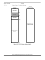
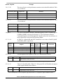
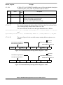
Freescale Semiconductor
Addendum
Document Number: MPC8245R2UMAD
Rev. 2.3, 04/2005
Errata to the MPC8245
Integrated Processor
User’s Manual, Rev. 2
This errata document describes corrections to the MPC8245 Integrated Processor User’s Manual, Rev. 2.
For convenience, errata items refer to the section and page numbers in the user’s manual. Items in bold are
new since the last revision of this document.
To locate any published updates for this document, refer to the world-wide web at http://freescale.com.
1
Document Revision History
Table 1 provides a revision history for this errata addendum.
NOTE
All errata in this document after that for E.2 on page 10 consist of an
appendix section that was omitted from the revision history of the MPC8245
Integrated Processor User’s Manual, Rev. 2. All errata in this document
from that point forward had already been corrected in the Rev. 2 manual.
.
Table 1-1. Document Revision History
Revision
Number
Date
2.1
—
Added new errata item for the following section: Appendix E, pages E35-E61
2.2
—
Added explanation about the previous user’s manual errata being added to Appendix E
2.3
04/05
Substantive Change
Added all errata for revision 2 of the reference manual except for item E.2 on page 10 detailing the
omission of the revision history information in Appendix E
© Freescale Semiconductor, Inc., 2005. All rights reserved.
Section, Page No.
2
Changes
Document Errata
The following section discusses new errata for the MPC8245 Integrated Processor User’s Manual, Rev. 2.
Section, Page
Changes
Throughout manual Whenever the dcbi instruction is mentioned, it should be accompanied by the
following note:
NOTE
The dcbi instruction should never be used on the G2 core.
2.2.2.17, 2-24
State Meaning
2.2.2.18, 2-25
Timing Comments
2.3.1, 2-40
2.3.2, 2-40
2.4, 2-44
The description for ‘State Meaning’ should be labeled ‘Timing Comments.’ The
following ‘State Meaning’ paragraph should be inserted immediately prior:
Asserted/Negated: The falling and rising edges of the AS signal provide a latch
strobe or edge reference to allow external devices to latch the data, address, or
control signals from the memory interface signals. AS is driven active for all
accesses to the ROM/Flash address space and the extended ROM/Flash address
space. This allows for Port X devices to share the address space with ROM
devices.
The following ‘Timing Comments’ paragraph should be inserted at the end of the
section:
Asserted: DRDY may be asserted anytime after a Port X strobe or handshake
access has begun, However, if DRDY is not asserted for a Port X handshake
transaction or for a period of time greater than the SDRAM refresh interval, the
memory may degrade and the memory controller will hang.
Negated: DRDY must be negated one clock cycle after RCSn is negated for the
Port X transaction.
Insert the following sentence after the first sentence of the last paragraph of this
section (immediately under the note):
PLL_CFG[0:4] signals must be driven on reset and must be held for at least
25 clock cycles after the negation of HRST_CTRL and HRST_CPU in order to be
latched.
Replace the last two sentences of the last paragraph on this page with the
following:
For the SDRAM sync loop (SDRAM_SYNC_OUT to SDRAM_SYNC_IN),
there is an inherent delay offset (Tos) that must be considered. The feedback trace
length of SDRAM_SYNC_OUT to SDRAM_SYNC_IN should be shortened to
reduce the impact of Tos. For more details on Tos, please refer to the hardware
specifications document.
Insert the following sentence immediately before the last sentence of this section:
PLL_CFG[0:4] signals must be driven on reset and must be held for at least
25 clock cycles after the negation of HRST_CTRL and HRST_CPU in order to be
latched.
Errata to the MPC8245 Integrated Processor User’s Manual, Rev. 2
2
Freescale Semiconductor
Section, Page No.
Changes
2.4, 2-45
In Table 2-5, the state meanings for the MDH signals have been modified to the
following:
Signal Name
Default
State Meaning
MDH[16:31]
x1
Sets the initial value of the PCI Subsystem Vendor ID register (at offset 0x2C). Note that
if this signal is not used for identifying a vendor ID, the default value can be used.
MDH[0:15]
x2
Sets the initial value of the PCI Subsystem ID register (at offset 0x2E). Note that if this
signal is not used for identifying a subsystem ID, the default value can be used.
1
The MDH[16:31] signals can be driven at reset to determine the initial value of the PCI Subsystem Vendor ID, but
alternatively they can be programmed after initialization.
2
The MDH[0:15] signals can be driven at reset to determine the initial value of the PCI Subsystem ID, but alternatively
they can be programmed after initialization.
4.2.2, 4-13
In Table 4-5, “Bit Settings for PCI Status Register—0x06,” the reset value of bit 7,
fast back-to-back enable, should be x. Also, the description should state:
This bit is hardwired to 1 on silicon revisions 1.2 (B) and earlier, 0 on silicon
revision 1.4. Note that, due to errata #20, type 2 fast back-to-back transactions are
not supported on the MPC8245.
In Table 4-17, the descriptions of PMCR1[CKO_MODE] and
PMCR1[CKO_SEL] should read as follows:
4.3.1, 4-20
1
2–1
CKO_MODE
00
Selects the clock source for the test clock output.
00 Disables the test clock output driver. Note that, in this case, there is no clock
output on CKO regardless of the setting of CKO_SEL (bit 0).
01 Selects the internal sys_logic_clk signal as the test clock output source
10 Selects one-half of the PCI rate clock as the test clock output source
11 Selects the internal PCI rate clock as the test clock output source
0
CKO_SEL
x1
The initial value of this bit is determined by the AS reset configuration bit, which
selects either the clock output of the processor core or the clock output of the
system logic to be driven out of the CKO signal.
0 Processor core clock selected. The signal driven by CKO is determined by
HID0[ECLK,SBCLK]. See Section 1.3.1.2.1, “Hardware
Implementation-Dependent Register 0 (HID0),” for the available choices.
1 System logic clock selected. The signal driven by CKO is determined by the
encoding of the CKO_MODE bits above. See CKO_MODE field description for
the available choices.
Note that if CKO_MODE (bits 2–1) are set to 00, there is no clock output on CKO
regardless of the setting of this bit.
Initial value depends on reset configuration signal. See Section 1.4, “Configuration Signals Sampled at Reset.”
4.4, 4-23
In Table 4-19, the reset value of DRV_PCI_CLK[1–2] (bits 3–2) should be
changed from 1 to 11.
Also in Table 4-19, the description of bits 1–0 should read: “Controls drive
strength of SDRAM_CLK[0:3] and SDRAM_SYNC_OUT for silicon revision
1.2 and later”
Errata to the MPC8245 Integrated Processor User’s Manual, Rev. 2
Freescale Semiconductor
3
Section, Page No.
Changes
4.7, 4-34
In Table 4-31, “Bit Settings for PICR2—0xAC,” bit 0 is no longer reserved; the
bit name is CB_OPT. The affected rows of the table should read as follows:
Bits
Name
Reset
Value
1
—
0
Reserved
0
CB_OPT
0
AC[0]—Copyback optimization
0 CCU can start the speculative read (or prefetch) of the next cache line (for PCI read
streaming purposes), even if the copyback buffer has valid data
1 CCU will not start the speculative read (or prefetch) of the next cache line (for PCI
read streaming purposes), until the copyback buffer is invalidated
4.8.2, 4-39
Description
In Table 4-37, “Bit Settings for Error Enabling Register 2 (ErrENR2)—0xC4,” bit
6 is no longer reserved; the bit name is PCI SERR enable. (This change applies
only to silicon revision 1.4.) The affected rows of the table should read as follows:
Bits
Name
Reset
Value
6
PCI SERR enable
0
Functional only in silicon revision 1.4.
This bit enables the reporting of SERR assertions that occur on the PCI bus at any
time regardless of whether the MPC8245 is the initiator, the target, or a
non-participating agent.
0 SERR detection is disabled
1 SERR detection is enabled
5–4
—
00
Reserved
4.8.2, 4-40
Description
In Table 4-38, “Bit Settings for Error Detection Register 2 (ErrDR2)—0xC5,” bit
6 is no longer reserved; the bit name is PCI SERR error. (This change applies only
to silicon revision 1.4.) The affected rows of the table should read as follows:
Bits
Name
Reset
Value
6
PCI SERR error
0
Functional only in silicon revision 1.4.
This bit indicates the assertion of SERR by an external PCI agent regardless of
whether the MPC8245 is the initiator, the target, or a non-participating agent.
0 SERR not detected
1 SERR detected
5–4
—
00
Reserved
Description
Errata to the MPC8245 Integrated Processor User’s Manual, Rev. 2
4
Freescale Semiconductor
Section, Page No.
Changes
4.9, 4-44
In Table 4-41, “Extended ROM Configuration Register 1—0xD0,” the description
of bits 9–5 (RCS2_ASRISE) should read as follows:
Bits
Name
Reset
Value
9–5
RCS2_ASRISE
All 0s
9–5
RCS2 AS rise time.These bits control how long AS is held asserted, or when the
AS signal is negated relative to the assertion of AS for the Port X interface. See
Section 1.3.5, “Port X Interface,” for more information.
00000 Disables AS signal generation
00001 1 clock
00010 2 clocks
00011 3 clocks
...
11111 31 clocks
Also in Table 4-41, the description column of row ‘RCS2_TS_WAIT_TIMER’
should be modified as follows: A note should be added to the table entitled ‘Wait
States for ROM High Impedance.’ The note applies to the columns ‘Reads with
gather data path in registered buffer mode (8, 16, 32-bit)’ and ‘All Flash writes 1,2
and reads with gather data path in inline buffer mode (8, 16, 32,-bit),’ and should
read as follows:
Note that TS_WAIT_TIMER only applies to gather data path reads when using
independent or base timing (RCS2_CTL = 0n); TS_WAIT_TIMER has no effect
on gather data path reads in Port X strobe or handshake modes (RCS2_CTL = 1n).
In Table 4-42, “Extended ROM Configuration Register 2—0xD4,” the description
of bits 9–5 (RCS3_ASRISE) should read as follows:
4.9, 4-47
Bits
Description
Reset
Value
Name
RCS3_ASRISE
All 0s
Description
RCS3 AS rise time.These bits control how long AS is held asserted, or when the
AS signal is negated relative to the assertion of AS for the Port X interface. See
Section 1.3.5, “Port X Interface,” for more information.
00000 Disables AS signal generation
00001 1 clock
00010 2 clocks
00011 3 clocks
...
11111 31 clocks
Also in Table 4-42, the description column of row ‘RCS3_TS_WAIT_TIMER’
should be modified as follows: A note should be added to the table entitled ‘Wait
States for ROM High Impedance.’ The note applies to the columns ‘Reads with
gather data path in registered buffer mode (8, 16, 32-bit)’ and ‘All Flash writes 1,2
and reads with gather data path in inline buffer mode (8, 16, 32,-bit),’ and should
read as follows:
Note that TS_WAIT_TIMER only applies to gather data path reads when using
independent or base timing (RCS3_CTL = 0n); TS_WAIT_TIMER has no effect
on gather data path reads in Port X strobe or handshake modes (RCS3_CTL = 1n).
Errata to the MPC8245 Integrated Processor User’s Manual, Rev. 2
Freescale Semiconductor
5
Section, Page No.
Changes
4.10, 4-51
In Table 4-45, “Bit Settings for the AMBOR—0xE0,” the description of
DLL_RESET (bit 5) should read as follows:
Bits
Name
Reset
Value
5
DLL_RESET
0
Description
Used to reset the DLL tap point. See Section 1.3.2, “DLL Operation and Locking.” This
bit must be explicitly set and then cleared by software during initialization in order to
guarantee correct operation of the DLL and the SDRAM_CLK[0:3] signals (if they are
used). The toggling of this bit needs to occur after the DLL mode has been chosen
using bit 7 of 0x72 and bit 2 of 0x76. See the hardware specification document for
more details on the DLL locking modes and their related graphs.
0 DLL tries to lock the phase between the SDRAM_SYNC_IN signal and the internal
sys_logic_clk signal.
1 The SDRAM_CLK signals are driven from tap point 0 of the internal delay line.
Also in Table 4-45, bit 0 is no longer reserved; the bit name is PCMWB_OPT. The
affected rows of the table should read as follows:
Bits
Name
Reset
Value
1
—
0
Reserved
0
PCMWB_OPT
0
E0[0]—PCMWB optimization—1
0 CCU can start the speculative read (or prefetch) of the next cache line (for PCI read
streaming purposes), even if any PCMWBs have valid data
1 CCU will not start the speculative read (or prefetch) of the next cache line (for PCI
read streaming purposes), until all PCMWBs are invalidated
4.13, 4-53
5.4.3.1, 5-26
6.2.9, 6-28
6.3.4, 6-62
Description
The register at offset 0xE3 should be called the DLL tap count register (DTCR).
The title of Table 4-48 should be: ‘Bit Settings for the DTCR—0xE3.’
In Table 4-48, “Bit Settings for this Register—0xE3,” add the following sentence
to the end of the description for DLL_TAP_COUNT (bits 6–0): See Section 6 of
AN2164, MPC8245/MPC8241 Memory Clock Design Guidelines: Part 1, for
details on the use of these bits.
In Table 5.5, the row listing eieio should be deleted.
Insert the following sentence after the first sentence of paragraph 2 (beginning
with the words “Because RMW parity assumes....”):
RWM parity is not supported when in 32-bit data path mode.
Replace the last paragraph immediately before Section 6.3.4.1 (paragraph begins
with ‘TS_WAIT_TIMER represents wait states....’) with the following:
TS_WAIT_TIMER represents wait states in the recovery time for certain ROM
accesses. Some ROM/Flash/Port X devices require long output disable timing. To
avoid contention, TS_WAIT_TIMER can be used to delay a subsequent data
transaction start on the local memory bus to allow the slow device to stop driving
the data bus. The delay is enforced for all local memory accesses (SDRAM or
ROM) that require a data tenure after most accesses to ROM space. The default
Errata to the MPC8245 Integrated Processor User’s Manual, Rev. 2
6
Freescale Semiconductor
Section, Page No.
6.3.5.2, 6-70
6.3.5.4, 6-71
6.3.5.4, 6-72
7.1, 7-2
7.7.4, 7-37
Changes
number of wait states is 2 clocks. TS_WAIT_TIMER applies under the following
conditions:
• If the ROM has a wide data bus (that is, 64-/32-bit, non-gathered),
TS_WAIT_TIMER applies to all read/write transactions.
• If the ROM has a narrow data bus (that is, 8-/16-/32-bit, gathered data path),
TS_WAIT_TIMER applies to all write transactions. However, for read
transactions, TS_WAIT_TIMER applies only when using the independent or
base timing modes (RCSn_CTL = 0n); TS_WAIT_TIMER has no effect
following reads in Port X strobe and handshake modes (RCSn_CTL = 1n).
• Regardless of the data bus width, TS_WAIT_TIMER only holds off subsequent
transactions that require a data tenure. SDRAM address-only or command
cycles such as bank-activate or refresh do not wait for TS_WAIT_TIMER to
expire.
The title of Figure 6-47 should be Port X 8-Bit Read Access Timing.
Replace the second sentence of the second paragraph (paragraph begins with the
words ‘In Port X handshake mode, ....’) with the following:
While RCSn is held asserted until DRDY is asserted, AS is negated 4 clocks after
DRDY is asserted or when RCSn_ASRISE is exceeded, whichever occurs first.
Replace the first sentence of the first paragraph after Figure 6-50 (begins with the
words ‘ASFALL is the only relevant timing parameter....’) with the following:
ASFALL and ASRISE are the relevant timing parameters in Port X handshake
mode; the ROMFAL parameter is ignored. Note that the assertion of DRDY may
terminate AS assertion earlier than the ASRISE interval.
In the third paragraph after the note (paragraph begins with the words ‘The
MPC8245 also provides ....’), replace the third sentence with the following:
Host mode supports only outbound address translation.
Replace the second sentence of the paragraph with the following:
Inbound and outbound address translation are both supported in agent mode;
however, in host mode, only outbound address translation is supported.
Errata to the MPC8245 Integrated Processor User’s Manual, Rev. 2
Freescale Semiconductor
7
Section, Page No.
Changes
In Figure 10-8, “Example I2C Interrupt Service Routine Flowchart,” replace the
two occurrences of I2CCR[MAL] with I2CSR[MAL]. The figure should look as
follows:
10.4.8, 10-19
Clear I2CSR[MIF]
== 1
I2CCR[MTX]
A
== 1
Master Xmit
Y
== 1
Last byte
I2CSR[RXAK]
== 0
End of address phase for
master receive mode?
N
Y
Write next byte
to I2CDR
Y Only one byte
to receive?
Clear
I2CCR[TXAK]
I2CSR[MAL]
N
Clear I2CSR[MAL]
== 1
Generate
STOP
== 0
== 0
I2CCR[MSTA]
N
Set
I2CCR[TXAK]
I2CSR[MAAS]
== 0
== 0
I2CSR[MAAS]
== 1
== 1
B
== 0
B
EOI
Slave Data Cycle
Slave Xmit
== 1
== 1
I2CCR[MTX] == 0
Slave Received
I2CSR[RXAK]
Read I2CDR
and store
== 0
Clear I2CCR[MTX]
N
Clear I2CCR[MTX]
Read I2CDR
(dummy read)
Write next byte
to I2CDR
Read I2CDR
(dummy read)
Set I2CCR[TXAK]
EOI
EOI
A
Master Rcv
All done
Y
N
B
Y
Last byte
Y Next-to-last N
byte
Slave Addr. Phase
== 1
Generate
STOP
Set
I2CCR[TXAK]
I2CSR[SRW]
Set I2CCR[MTX]
== 0
Clear I2CCR[MTX]
Dummy read
Write I2CDR
Read I2CDR
and store
EOI
EOI
Figure 10-8. Example I2C Interrupt Service Routine
Errata to the MPC8245 Integrated Processor User’s Manual, Rev. 2
8
Freescale Semiconductor
Section, Page No.
Changes
12.4.9, 12-23
In Table 12-15, change the last sentence in the description for the BI field (bit 4)
to read:
Note that for the non-FIFO mode, after the ULSR is read, ULSR[BI] is
immediately set if the bus remains zero and no mark state followed by a valid new
character has been detected.
In Table 16-3, “Monitor Mode Control Register (MMCR)” change the description
of bits 6 and 0 as follows:
16.2.2, 16-4
Bits
Name
6
DISCOUNT
5–1
—
0
PMCTRIG
Reset Value R/W
1’b0
Description
RW Disable counter for msb bit. This bit determines the counting behavior of all
counters when any counter reaches a negative value (most significant bit is set).
0 No effect on the counters
1 All the counters are disabled if any of PMC0–PMC3 has bit 31 set and
MMCR[PMCTRG] = 0
Reserved
1’b0
RW Performance monitor counter trigger. This bit determines the behavior of all
counters if any reach a negative value (most significant bit is set).
0 No effect on counters if MMCR[DISCOUNT] is clear; otherwise see description
MMCR[DISCOUNT] for expectations if it is set and this bit is clear.
1 Counting of PMC1, PMC2, and PMC3 will begin only when msb of any
PMC0–PMC3 are set and stop when msb of all PMC0–PMC3 are cleared.
PMCTRG may be used as a triggering mechanism (use PMC0 to define the
triggering event) to allow counting after a certain condition occurs or after enough
time has elapsed. Note that because all the counters are writable, when this bit is
set, if the msb of any of the counters are written to, all the remaining counters begin
counting. Incrementing of the counters will continue until the last of all the counters
have a positive value.
Errata to the MPC8245 Integrated Processor User’s Manual, Rev. 2
Freescale Semiconductor
9
Section, Page No.
Changes
NOTE
The following erratum contains an appendix section that was omitted from
the revision history of the MPC8245 Integrated Processor User’s Manual,
Rev. 2. It contains only errata that had already been corrected in the Rev. 2
manual.
E.2, E-35
E.2
Add new section E.2 with the following text that details the revision history from
Rev. 0 to Rev. 1 of the user’s manual. (This section was omitted from Rev. 2.0 of
the user’s manual.)
Revision Changes From Revision 0 to Revision 1
Major changes to the MPC8245 Integrated Processor User’s Manual from Revision 0 to Revision 1 are as
follows:
Section, Page
1.1.1, 1-4
Changes
The second bullet under the Memory Interface heading should state:
– High-bandwidth data bus (32- or 64-bit) to SDRAM
The fourth bullet under the Memory Interface heading should state:
– Supports 1 to 8 banks of 16-, 64-, 128-, 256-, or 512-Mbit memory devices
The second to the last bullet under the Memory Interface heading should state:
– Extended ROM space supports 8-, 16-, or 32-bit gathering data path, 32- or
64-bit (wide) data path
The second to the last bullet under the 32-bit PCI interface heading should be
replaced with the following sentence:
– Address translation with two inbound and outbound units (ATU)
The second to the last bullet under the Two-channel Integrated DMA Controller
(Writes To ROM/PORTX Not Supported) heading should be replaced with the
following:
– Local-to-PCI memory
The following statement should be added to the list of Debug Features:
– Error injection/capture on data path
Sections that describe signals SDMA13 and SDMA14 have been added to this
chapter:
1.1.1, 1-4
1.1.1, 1-4
1.1.1, 1-4
1.1.1, 1-5
1.1.1, 1-5
2.1.1, 2-6
Signal
Signal Name
Interface
…
…
…
SDMA13
SDRAM address 13
Memory
SDMA14
SDRAM address 14
Memory
…
…
…
Alternate
Function(s)
Pins
I/O
Section #
…
…
…
…
See Table 6-2
1
O
2.2.2.a
1
O
2.2.2.b
…
…
…
…
Errata to the MPC8245 Integrated Processor User’s Manual, Rev. 2
10
Freescale Semiconductor
Section, Page No.
Changes
2.1.2, 2-7
In Table 2-2, Signals SDMA12/SRESET, SDMA12/TBEN,
SDMA14/CHKSTOP_IN are driven if extended addressing mode is enabled.
2.2.2.4 and 2.2.2.5, 2-18
The last sentence of the state meanings for SDRAM Address (SDMA[11:0]) and
SDRAM Address 12 (SDMA12) should state:
See Section 6.2.2, “SDRAM Address Multiplexing,” Section 6.3.1.1, “Base ROM
Address Multiplexing,” and Section 6.3.2.1, “Extended ROM Address
Multiplexing,” for a complete description of the mapping of these signals in all
cases.
2.2.2.5, 2-18
The following sentence should be added to the first paragraph of this section:
“SDMA12 is used in extended addressing mode. See Section 6.2.2, “SDRAM
Address Multiplexing” and Section 2.4, “Configuration Signals Sampled at
Reset,” for more information.”
2.2.2.6, 2-18
The following signal descriptions of SDMA13 and SDMA14 should be added to
this chapter after the SDMA12 description:
2.2.2.a SDRAM Address 13 (SDMA13)—Output
The SDMA13 signal is similar to SDMA[11:0] in that it corresponds to different
row or column address bits, depending on the memory in use. SDMA13 is
multiplexed with TBEN and is used in extended addressing mode. See Section
6.3.2, “Extended ROM Interface,” for more information.
State Meaning
Asserted/Negated: See Section 6.3.2.1, “Extended ROM Address Multiplexing,”
for a complete description of the mapping of this signal in all cases.
Timing Comments
Assertion/Negation: The same as SDMA[11:0].
2.2.2.b SDRAM Address 14 (SDMA14)—Output
The SDMA14 signal is similar to SDMA[11:0] in that it corresponds to different
row or column address bits, depending on the memory in use. SDMA14 is
multiplexed with CHKSTOP_IN and is used in extended addressing mode. See
Section 6.3.2, “Extended ROM Interface,” for more information.
State Meaning
Asserted/Negated: See Section 6.3.2.1, “Extended ROM Address Multiplexing,”
for a complete description of the mapping of this signal in all cases.
Timing Comments
Assertion/Negation: The same as SDMA[11:0].
2.2.5, 2-25
The following sentences should be added to the first paragraph of this section:
“The signals SIN1, SOUT1, SIN2/CTS1, and SOUT2/RTS1 are multiplexed with
PCI_CLK0, PCI_CLK1, PCI_CLK2, and PCI_CLK3, respectively. Note that
when using DUART signals, PCI_CLK[0:3] signals cannot be used.”
Errata to the MPC8245 Integrated Processor User’s Manual, Rev. 2
Freescale Semiconductor
11
Section, Page No.
2.2.6.2, 2-27
2.2.6.3, 2-27
2.2.6.3, 2-28
2.2.6.6, 2-28
2.2.6.7, 2-29
2.2.8.2, 2-34
2.3.2, 2-37
Changes
The last sentence of the first paragraph of this section should be replaced with the
following:
“Note that the SRESET signal is multiplexed with the SDMA12 signal. In
extended addressing mode, SDMA12 is used and SRESET is not available. See
Section 6.3.2, “Extended ROM Interface,” for more information.”
The following sentence should be added to the first paragraph of this section:
“Note that the output driver for MCP can be designated as open-drain by setting
the MIOCR[MCP_OD_MODE] parameter.”
PMCR2[SHARED_MCP] should be replaced with MIOCR[MCP_OD_MODE]
in the last paragraph of this section as follows:
“High impedance: If the MIOCR[MCP_OD_MODE] bit is set, the MCP signal is
placed in high impedance when there is no error to report.”
The following sentences should be added to the first paragraph of this section:
“Note that the CHKSTOP_IN signal is multiplexed with the SDMA14 signal. In
extended addressing mode, SDMA14 is used and CHKSTOP_IN is not available.
See Section 6.3.2, “Extended ROM Interface,” for more information.”
The first paragraph should state:
“Following are the state meaning and timing comments for TBEN. Note that the
TBEN signal is multiplexed with the SDMA13 signal. In extended addressing
mode, SDMA13 is used and TBEN is not available. In this case, PICR1[DEC] can
be used to enable the processor core’s decrementer. See Table 4-31 for a
description of PICR1[DEC].”
The following sentence should be added to this section:
“Note that PCI_CLK[0:3] cannot be used when using DUART signals SIN1,
SOUT1, SIN2/CTS1, and SOUT2/RTS1.”
The fourth paragraph of this section should state:
“In order to insure proper operation and successful locking of the DLL, there are
certain requirements that must be met as described in the MPC8245 Hardware
Specification. In some cases (depending on the board layout and the frequencies),
the DLL lock range must be lengthened by setting the
MIOCR1[DLL_MAX_DELAY] bit described in Section 4.5, “Output/Clock
Driver and Miscellaneous I/O Control Registers.” This is accomplished by
increasing the time between each of the 128 tap points in the delay line. Although
this increased time makes it easier to guarantee that the reference clock is within
the DLL lock range, it also means there may be slightly more jitter in the output
clock of the DLL, should the phase comparator shift the clock between adjacent
tap points. ”
Errata to the MPC8245 Integrated Processor User’s Manual, Rev. 2
12
Freescale Semiconductor
Section, Page No.
Changes
2.4, 2-40
In Table 2-5, the state meaning of signal MAA0 should be as follows:
Signal Name
Default
…
…
…
MAA0
1
Address map setting. This signal should always be pulled high since the MPC8245 only
supports address map B.
1 The MPC8245 is configured for address map B.
…
…
…
2.4, 2-41
State Meaning
In Table 2-5, the default value of signal PMAA2 is 0, as follows:
Signal Name
Default
…
…
…
PMAA2
0
Driver capability for the PCI and EPIC controller output signals. The value of this signal
sets the initial value of ODCR[DRV_PCI].
0 40 Ω drive capability on PCI/EPIC signals
1 20 Ω drive capability on AD[31:0], C/BE[3:0], DEVSEL, FRAME, GNT[4:0], PAR,
INTA, IRDY, PERR, SERR, STOP, TRDY, IRQ0/S_INT, IRQ1/S_CLK, and IRQ4/L_INT
signals and 6 Ω drive capability on IRQ2/S_RST and IRQ3/S_FRAME
…
…
…
2.4, 2-41
State Meaning
In Table 2-5, the second sentence of the SDMA1 state meaning should state the
following:
Signal Name
Default
State Meaning
…
…
…
SDMA1
1
Extended addressing mode. When this signal is low during reset, the extended
addressing mode is enabled. The value of this signal during reset determines the
function of the SRESET, TBEN, CHKSTOP_IN, TRIG_IN, and TRIG_OUT signals. See
6.3.2, “Extended ROM Interface,” for more information on the multiplexing of these
signals.
0 Extended addressing mode enabled. SDMA12, SDMA13, SDMA14, RCS2, and
RCS3 signals are available.
1 Extended addressing mode disabled. SRESET, TBEN, CHKSTOP_IN, TRIG_IN, and
TRIG_OUT are available.
…
…
…
In Table 3-2, PCI memory transaction address range 7000_0000–7FFF_FFFF has
a local memory address range of 7000_0000–7FFF_FFFF as follows:
3.1, 3-2
PCI Memory Transaction Address Range
Hex
…
Decimal
…
…
…
Local Memory
Address Range
…
Definition
…
Errata to the MPC8245 Integrated Processor User’s Manual, Rev. 2
Freescale Semiconductor
13
Section, Page No.
Changes
PCI Memory Transaction Address Range
Hex
Local Memory
Address Range
Decimal
Definition
7000_0000
7FFF_FFFF
2G - 256M
2G - 1
7000_0000–7FFF_FFFF
…
…
…
…
…
3.1, 3-4
Extended ROM/Flash (256
MBytes)11
…
In Figure 3-1, the memory controller range between 2GB and 4GB – 32MB
should state “Forwards to PCI memory space,” as follows:
MPC8245
Memory Controller
Processor
0
Local
memory space
0 to 2GB - 256MB
Local
memory
Not forwarded
to PCI bus.
Memory controller
performs local
memory access
Reserved
PCI Memory Space
0
Not addressable by
processor
2GB - 256MB
Extended ROM
Extended ROM
2GB
Forwards to PCI
Memory Space
PCI memory space in
range
2 to 4GB - 32MB
Not addressable by
processor
2GB
4GB - 32MB
4GB - 16MB
If local ROM,
not addressable as
PCI memory.
If remote ROM,
PCI memory space
PCI Memory Space
4GB
PCI I/O Space
4GB - 32MB
PCI I/O Space
4GB - 32MB + 64KB Clears A[31:24] and
forwards to PCI I/O
space, except
0xFE01_0000–
4GB - 24MB
0xFE7F_FFFF,
which is reserved
PCI I/O Space
CONFIG_ADDR
CONFIG_DATA
PCI Int Ack
ROM or Flash
0
I/O addresses in
0 to 64KB range
64KB
8MB
I/O addresses in
8MB to 12MB range
4GB - 20MB
4GB - 18MB
4GB - 17MB
4GB - 16MB
4GB
12MB
PCI Configuration
Access
Int Ack Broadcast PCI
Not addressable by
processor
ROM Access
4GB
Errata to the MPC8245 Integrated Processor User’s Manual, Rev. 2
14
Freescale Semiconductor
Section, Page No.
3.1, 3-6
Changes
Replace Figure 3-3 with the following:
PCI Master
I/O Space
MPC8245
Memory Controller
0
Addressable by
processor
64KB
Reserved
8MB
Addressable by
processor
12MB
MPC8245 does not
respond as a target
to PCI I/O accesses
Not addressable by
processor
4GB
Figure 3-3. PCI I/O Master Address Map B
Errata to the MPC8245 Integrated Processor User’s Manual, Rev. 2
Freescale Semiconductor
15
Section, Page No.
Changes
3.4.1, 3-26
The cross reference to the performance monitor section should be added to Table
3-13 as follows:
Local Memory Offset
Register Set
…
…
Reference
…
0xF_E000 – 0xF_EFFF Performance monitor Section 16.2.3, “Performance Monitor Counter (PMC0–PMC3)”
…
…
3.4.2, 3-27
The cross reference to the performance monitor section should be added to Table
3-14 as follows:
PCI Memory Offset
Register Set
…
…
0xE00 – 0xEFF
Performance monitor
…
…
Chapter 4
…
0xDC
…
Section 16.2.3, “Performance Monitor Counter (PMC0–PMC3)”
…
Program
Access
(Bytes)
…
…
…
…
…
Extended ROM configuration register 3
4
4
Read/Write
0x0C00_000E
Register
Access
Reset Value
Extended ROM configuration register 4
4
4
Read/Write
0x0800_000E
…
…
…
…
…
4.2.8, 4-15
The description of this register in Table 4-12 should read as follows:
Bits
Reset Value
msb 15–0
x1
Description
Value is determined at startup through configuration pins MDH[16:31] but can be
programmed by software after reset.
Initial value depends on reset configuration signal. See Section 2.4, “Configuration Signals Sampled at Reset.”
4.2.9, 4-15
1
…
Size
(Bytes)
Address
Offset
0xD8
Reference
The correct Performance Monitor Command Registers are the 4 CMDR registers
(CMDR0-CMDR3) referenced in Section 16.2. The Performance Monitor
Command Registers at 0x48 through 0x5C should not be used. Any reference to
these registers have been removed from this chapter.
In Table 4-1, offsets 0xD8 and 0xDC should have reset values of 0x0C00_000E
and 0x0800_000E, respectively.
4.1.3.1, 4-6
1
…
Table 4-13 should be titled “Table 4-13. Subsystem ID—0x2E and the description
of this register should read as follows:
Bits
Reset Value
msb 15–0
x1
Description
Value is determined at startup through configuration pins MDH[0:15] but can be
programmed by software after reset.
Initial value depends on reset configuration signal. See Section 2.4, “Configuration Signals Sampled at Reset.”
Errata to the MPC8245 Integrated Processor User’s Manual, Rev. 2
16
Freescale Semiconductor
Section, Page No.
Changes
4.2.11, 4-16
Table 4-15 should contain the following description for bit 5 of the PGCR:
Bits
Reset
Value
…
…
…
5
0
R/W
…
…
…
4.4.2, 4-23
R/W
Description
…
Controls ability to retry all incoming PCI read transactions to local memory while the
processor core is writing data to the PCI bus (for example, while internal buffers have data to
be written to the PCI bus).
0 Disables ability to retry all incoming PCI memory read transactions to local memory while
the processor core is writing data to the PCI bus.
1 Enables ability to retry all incoming PCI memory read transactions to local memory while
the processor core is writing data to the PCI bus.
…
In figure 4-9, PCI_HOLD_DELAY[0-1] should include bits 5-4 as follows:
Reserved
PLL_SLEEP
PCI_HOLD_DELAY[0–1]
DLL_EXTEND
0
7
4.4.2, 4-23
1
6
0
5
4
3
00
2
1
0
Bits 6-4 of power management configuration register 2 should be updated as
follows:
Bits
Reset Value
R/W
Description
…
…
…
…
Reserved
6
—
0
5–4
PCI_HOLD_DEL
xx1
PCI output hold delay value relative to the PCI_SYNC_IN signal. See the
MPC8245 Hardware Specification for the detailed number of nanoseconds
guaranteed for each setting. There are eight sequential settings for this value;
each corresponds to a set increase in hold time:
00 Recommended for 66 MHz PCI bus (default)
01
10 Recommended for 33 MHz PCI bus
11
The initial values of bits 5 and 4 are determined by the inverse of MCP and CKE
reset configuration signals, respectively. See Section 2.4, “Configuration Signals
Sampled at Reset,” for more information. As these two pins have internal pull-up
resistors, the default value after reset is 0b00.
…
…
…
…
Initial value depends on reset configuration signal. See Section 2.4, “Configuration Signals Sampled at Reset.”
4.5, 4-24 and 4-25
Table 4-21 should be updated as follows:
Bit 6 of the output driver control register has been renamed DRV_STD_MEM.
Bits 5-4, DRV_MEM_CTRL[1-2], only drive SDRAM_CLK[0:3] and
SDRAM_SYNC_OUT signals for silicon revision 1.1.
Errata to the MPC8245 Integrated Processor User’s Manual, Rev. 2
Freescale Semiconductor
17
Section, Page No.
Changes
Bits 1-0, DRV_MEM_CLK[1-2], should be added to the table.
Please note these changes in the table below:
1
Bits
Name
Reset
Value
msb 7
addr<73>
DRV_PCI
x1
Driver capability for the PCI and EPIC controller output signals.
0 40 Ω drive capability on PCI/EPIC signals
1 20 Ω drive capability on AD[31:0], C/BE[3:0], DEVSEL, FRAME,
GNT[4:0], PAR, INTA, IRDY, PERR, SERR, STOP, TRDY,
IRQ0/S_INT, IRQ1/S_CLK, and IRQ4/L_IN signals and 6 Ω drive
capability on IRQ2/S_RST and IRQ3/S_FRAME
The initial value of this bit is determined by the PMAA2 reset
configuration pin.
6
DRV_STD_MEM
1
Driver capability for standard and memory signals (PMAA[0:2], SDA,
SCL, CKO, QACK, DA[10:6], MCP, MDH[0:31], MDL[0:31], PAR[0:7],
and MAA[0:2])
0 40 Ω drive capability on standard signals
1 20 Ω drive capability on standard signals
5–4
DRV_MEM_CTRL[1–2]
xx1
3–2
DRV_PCI_CLK[1–2]
1
Controls drive strength of PCI_CLK[0:4] and PCI_CLK_SYNC_OUT.
DRV_PCI_CLK[1–2]:
00 reserved
01 40-Ω drive capability
10 20-Ω drive capability
11 6-Ω drive capability
1–0
DRV_MEM_CLK_[1–2]
11
Controls drive strength of SDRAM_CLK[0:3] and SDRAM_SYNC_OUT
for silicon revision 1.2
DRV_MEM_CLK_[1–2]:
00 reserved
01 40-Ω drive capability
10 20-Ω drive capability
11 6-Ω drive capability
Description
Driver capability for the memory signals (CS[0:7], DQM[0:7], WE, FOE,
RCS0, RCS1, SDBA[1:0], SDRAS, SDCAS, CKE, AS, and SDMA[11:0],
CHKSTOP_IN, SRESET, TBEN,TRIG_OUT.
Controls drive strength of SDRAM_CLK[0:3] and SDRAM_SYNC_OUT
for silicon revision 1.1
DRV_MEM_CTRL[1–2]:
00 reserved
01 40-Ω drive capability
10 20-Ω drive capability
11 6-Ω drive capability
The initial value of DRV_MEM_CTRL[1–2] is determined by the PMAA0
and PMAA1 reset configuration pins, respectively.
See Initial value depends on reset configuration signal. See Section 2.4, “Configuration Signals Sampled at Reset.”
4.5, 4-25
In Table 4-22, the description for bit 15 should state that it disables/enables the
PCI_SYNC_OUT signal of the MPC8245 as follows:
Bits
Name
Reset
Value
15
addr<75>
PCI_SYNC_OUT
0
Description
This bit disables/enables the PCI_SYNC_OUT signal of the MPC8245. A value
of one (0b1) disables the output. A value of zero (0b0) enables the output.
Errata to the MPC8245 Integrated Processor User’s Manual, Rev. 2
18
Freescale Semiconductor
Section, Page No.
Changes
4.5, 4-26
In Table 4-23, bit 5 of MIOCR1 should be reserved. Also note that the description
of MIOCR1[DLL_MAX_DELAY] should be added as follows:
Bits
Name
Reset
Value
…
…
…
5–3
—
000
2
DLL_MAX_DELAY
0
This bit can be used to set the delay line length. Please see Section 2.3.2, “DLL
Operation and Locking,” for more information.
0 shorter (or normal) DLL delay line length
1 DLL_max_mode, longer DLL delay line length
…
…
…
…
4.7.1, 4-27
Description
…
Reserved
The extended starting and ending address fields have three bits as shown below.
The section originally showed these fields as two bits.
The correct formulas for the lower and upper boundaries are as follows:
Lower boundary for bank n = 0b0 || <extended starting address n> || <starting address n> || 0x0_0000.
and
Upper boundary for bank n = 0b0 || <extended ending address n> || <ending address n> || 0xF_FFFF.
4.7.1, 4-28
The correct figures for the extended memory starting address registers are as
follows:
Reserved
Extended Starting Address 1
Extended Starting Address 2
Extended Starting Address 3
0000_0
31
Extended Starting Address 0
0000_0
27 26
24 23
0000_0
19 18
16 15
0000_0
11 10
8
7
3
2
0
Figure 4-12. Extended Memory Starting Address Register 1—0x88.
Reserved
Extended Starting Address 6
Extended Starting Address 5
Extended Starting Address 7
0000_0
31
Extended Starting Address 4
0000_0
27 26
24 23
0000_0
19 18
16 15
0000_0
11 10
8
7
3
2
0
Figure 4-13. Extended Memory Starting Address Register 2—0x8C
Errata to the MPC8245 Integrated Processor User’s Manual, Rev. 2
Freescale Semiconductor
19
Section, Page No.
4.7.1, 4-29
Changes
The correct bit settings for extended memory starting address registers 1 and 2 are
shown in table 4-27 as follows:
Bits
Name
Reset Value
31–27
—
All 0s
Reserved
26–24
Extended starting address 3
All 0s
Extended starting address for bank 3
23–19
—
All 0s
Reserved
18–16
Extended starting address 2
All 0s
Extended starting address for bank 2
15–11
—
All 0s
Reserved
10–8
Extended starting address 1
All 0s
Extended starting address for bank 1
7–3
—
All 0s
Reserved
2–0
Extended starting address 0
All 0s
Extended starting address for bank 0
31–27
—
All 0s
Reserved
26–24
Extended starting address 7
All 0s
Extended starting address for bank 7
23–19
—
All 0s
Reserved
18–16
Extended starting address 6
All 0s
Extended starting address for bank 6
15–11
—
All 0s
Reserved
10–8
Extended starting address 5
All 0s
Extended starting address for bank 5
7–3
—
All 0s
Reserved
2–0
Extended starting address 4
All 0s
Extended starting address for bank 4
4.7.1, 4-30
Description
Byte Address
0x88
0x8C
The correct figures for the extended memory ending address registers are as
follows:
Reserved
Extended Ending Address 2
Extended Starting Address 1
Extended Ending Address 3
Extended Ending Address 0
0000_0
31
0000_0
27 26
24 23
0000_0
19 18
16 15
0000_0
11 10
8
7
3
2
0
Figure 4-16. Extended Memory Ending Address Register 1—0x98
Reserved
Extended Ending Address 6
Extended Starting Address 5
Extended Ending Address 7
0000_0
31
Extended Ending Address 4
0000_0
27 26
24 23
0000_0
19 18
16 15
0000_0
11 10
8
7
3
2
0
Figure 4.17. Extended Memory Ending Address Register 2—0x9C
Errata to the MPC8245 Integrated Processor User’s Manual, Rev. 2
20
Freescale Semiconductor
Section, Page No.
Changes
4.7.1, 4-30 and 4-31
The correct bit settings for extended memory ending address registers 1 and 2 are
shown in table 4-29 as follows:
Bits
Name
Reset Value
31–27
—
All 0s
Reserved
Description
Byte Address
26–24
Extended ending address 3
All 0s
Extended ending address for bank 3
23–19
—
All 0s
Reserved
18–16
Extended ending address 2
All 0s
Extended ending address for bank 2
15–11
—
All 0s
Reserved
10–8
Extended ending address 1
All 0s
Extended ending address for bank 1
7–3
—
All 0s
Reserved
2–0
Extended ending address 0
All 0s
Extended ending address for bank 0
31–27
—
All 0s
Reserved
26–24
Extended ending address 7
All 0s
Extended ending address for bank 7
23–19
—
All 0s
Reserved
18–16
Extended ending address 6
All 0s
Extended ending address for bank 6
15–11
—
All 0s
Reserved
10–8
Extended ending address 5
All 0s
Extended ending address for bank 5
7–3
—
All 0s
Reserved
2–0
Extended ending address 4
All 0s
Extended ending address for bank 4
4.8, 4-33
0x98
0x9C
Figure 4-20 should include DEC, bit 8, as follows:
Reserved
Speculative PCI Reads
CF_APARK
0b1
LE_MODE
ST_GATH_EN
DEC
CF_DPARK
MCP_EN
FLASH_WR_EN
PROC_TYPE
RCS0
0b00
1111_1111
31
0
0
24 23 22 21 20 19 18 17 16 15
000
0
13 12 11 10 9
0
8
7
1
6
5
4
0
3
2
1
0
Figure 4-20. Processor Interface Configuration Register 1 (PIRC1)—0xA8
Errata to the MPC8245 Integrated Processor User’s Manual, Rev. 2
Freescale Semiconductor
21
Section, Page No.
Changes
4.8, 4-34
Table 4-32 should include a description of DEC as follows:
Bits
Name
Reset
Value
…
…
…
…
8
DEC
0
This bit can be used to enable the time base and decrementor of the
processor core. In extended addressing mode, the TBEN signal functions as
SDMA13. This bit can be used by software to enable the time base and
decrementor in the processor core.
0 Disable processor core decrementer in extended addressing mode
1 Enable processor core decrementer in extended addressing mode
…
…
…
…
4.9.2, 4-43
Description
In Table 4-40, the reference to MPC107 in the description of PCI SERR error
should be replaced with a reference to the MPC8245, as follows:
Bits
Name
Reset
Value
Description
…
…
…
…
6
PCI SERR error
0
This bit indicates the assertion of SERR by an external PCI agent regardless
of whether the MPC8245 is the initiator, the target, or a non-participating agent.
0 SERR not detected
1 SERR detected
…
…
…
…
4.10, 4-45 and 4-48
In Table 4-43 and Table 4-44, the description for RCS2_BURST and
RCS3_BURST should be replaced with the description below. Also, the
description for bit setting 01 of RCS2_DBW and RCS3_DBW should be as
follows:
Bits
Name
Reset
Value
Description
…
…
…
…
30
RCS n_BURST
0
Burst mode ROM chip-select n timing enable
0 Indicates standard (nonburst) ROM access timing
1 Indicates burst-mode ROM access timing. When burst mode is enabled,
ROM reads use RCSn_ROMNAL for burst beats.
29–28
RCSn_DBW
11
These bits control the of the data bus width for RCSn.
00 8-bit data path with gathering
01 16-bit data path with gathering
10 32-bit data path with gathering. Gathering occurs if DBUS0 = 1.
11 wide data path; 64-bit if DBUS0 = 1, 32-bit if DBUS0 = 0
…
…
…
…
Errata to the MPC8245 Integrated Processor User’s Manual, Rev. 2
22
Freescale Semiconductor
Section, Page No.
Changes
4.10, 4-46 and 4-49
Bits
In Table 4-43 and Table 4-44, bit setting 00000 for RCS2_ASFALL and
RCS3_ASFALL have a 0 clock falling time. Also note that bit setting 11111 for
RCS2_ASFALL, RCS3_ASFALL, RSC2_ASRISE, and RCS3_ASRISE has a 31
clock falling time as follows:
Reset
Value
Name
Description
…
…
…
14–10
RCS n_ASFALL
All 0s
RCSn AS fall time. These bits control the falling edge timing of the AS signal
relative to the falling edge of RCSn for the Port X interface. See Section
6.3.5, “Port X Interface,” for more information.
00000 0 clocks (AS asserted coincident with the chip select)
00001 1 clock
00010 2 clocks
00011 3 clocks
...
11111 31 clocks
9–5
RCSn_ASRISE
All 0s
RCSn AS rise time. These bits control the rising edge timing of the AS signal
relative to the falling edge of RCSn for the Port X interface. See Section
6.3.5, “Port X Interface,” for more information.
00000 Disables AS signal generation
00001 1 clock
00010 2 clocks
00011 3 clocks
...
11111 31 clocks
…
…
…
4.10, 4-51
…
…
In Figure 4-32, the RCSn_SADDR field is 16 bits long, as follows:
Reserved
RCSn_SIZE
RCSn_SADDR
0000
31
28 27
0000_0000
12 11
4
3
0
In Table 4-45 and Table 4-46, the RCS2_SADDR and RCS3_SADDR fields are
16 bits long as follows:
Bits
Reset
Value
Name
…
…
27–12
RCSn_SADDR
…
…
…
Description
…
0xC000 Starting address for RCSn in megabytes.
Physical starting address = 0x7 || RCS n_SADDR || 0x000
…
…
Table 4-46 should be titled “Table 4-46. Extended ROM Configuration Register
4—0xDC”
Errata to the MPC8245 Integrated Processor User’s Manual, Rev. 2
Freescale Semiconductor
23
Section, Page No.
Changes
4.12, 4-53
Section 4.12 should read as follows:
The PLL configuration register (PCR) indicates the values used to set the PLL
mode. See MPC8245 Hardware Specification for more information Figure 4-34
shows the bits of the PCR.
PLL_CFG
7
000
3
2
0
Figure 4-34. PLL Configuration Register (PCR)—0xE2
Table 4-48 shows the specific bit settings for the PLL Configuration Register.
Table 4-48. Bit Settings for the PCR—0xE2
1
Bits
Name
Reset
Value
7–3
PLL_CFG
x1
2–0
—
000
Description
PLL Configuration. Indicates the values used to set the PLL mode.
Reserved
Initial value depends on reset configuration signal. See Section 2.4, “Configuration Signals Sampled at Reset.”
4.13, 4-54
In Table 4-49, the description of MCCR1[DBUS_SIZ[0-1]] should be added as
follows:
Bits
Name
Reset
Value
…
…
…
…
xx
Read-only. This field indicates the state of the memory data path width. The value
of this field is determined by the reset configuration signals [DL[0], FOE]. Used
with DBUS_SIZ2 (stored in MCCR4[17]) as shown below.
DBUS_SIZ[0–2]:
For SDRAM:
0nn 32-bit data bus
1nn 64-bit data bus
22–21 DBUS_SIZ[0–1]
Description
For ROM/Flash chip select #0 (RCSO):
00n 32-bit data bus
n1n 8-bit data bus
10n 64-bit data bus
For ROM/Flash chip select #1 (RCS1):
0n0 32-bit data bus
nn1 8-bit data bus
1n0 64-bit data bus
For ROM/Flash chip select #2 (RCS2) and ROM/Flash chip select #3 (RCS3) data
bus width is set by ERCR1[RCS2_DBW] and ERCR2[RCS2_DBW], respectively.
…
…
…
…
Errata to the MPC8245 Integrated Processor User’s Manual, Rev. 2
24
Freescale Semiconductor
Section, Page No.
Changes
4.13, 4-58
In Table 4-50, the description of MCCR2[REFINT] is 14 bits long, as follows:
Bits
Name
Reset
Value
…
…
…
15–2
REFINT
All 0s
…
…
…
4.13, 4-59
Description
…
Refresh interval. These bits directly represent the number of clock cycles between
CBR refresh cycles. One row is refreshed in each RAM bank during each CBR
refresh cycle. The value for REFINT depends on the specific RAMs used and the
operating frequency of the MPC8245. See Section 6.2.12, “SDRAM Refresh,” for
more information. Note that the period of the refresh interval must be greater than
the read/write access time to ensure that read/write operations complete
successfully.
…
MCCR2[DBUS_SIZE[2]], bit 17, should be included in Figure 4-38 as follows:
Reserved
BUF_TYPE[1]
BUF_TYPE[0]
BSTOPRE[0–1]
WMODE
DBUS_SIZE[2]
PRETOACT
ACTOPRE
31
BSTOPRE[6–9]
REGDIMM
28 27
4.13, 4-60
0
0
SDMODE
24 23 22 21 20 19 18 17 16 15 14
ACTORW
8
7
4
3
0
In Table 4-52, the description of MCCR4[DBUS_SIZE[2]], bit 17 should be
added as follows:
Bits
Name
Reset
Value
…
…
…
…
17
DBUS_SIZE[2]
0
See description for bits 22–21 of MCCR1.
…
…
…
…
5.3.1.2.1, 5-16
Description
The following text and table should be added at the end of this section:
Table 5-2 shows how HID0[SBCLK], HID0[ECLK], and the hard reset signals are
used to configure CKO when PMCR1[CKO_SEL] = 0. When
PMCR1[CKO_SEL] = 1, the CKO_MODE field of PMCR1 determines the signal
driven on CKO. Note that the initial value of PMCR1[CKO_SEL] is determined
by the value on the AS signal at the negation of HRST_CPU. See Section 2.2.8.8,
“Debug Clock (CKO)—Output,” and Section 2.4, “Configuration Signals
Sampled at Reset,” for more information.
Errata to the MPC8245 Integrated Processor User’s Manual, Rev. 2
Freescale Semiconductor
25
Section, Page No.
Changes
Table 5-2. HID0[BCLK] and HID0[ECLK] CKO Signal Configuration
5.8, 5-33
Chapter 6
6.1, 6-5
6.2.2, 6-11
HRST_CPU and
HRST_CTRL
HID0[ECLK]
HID0[SBCLK]
Asserted
x
x
Processor core clock
Negated
0
0
High impedance
Negated
0
1
sys-logic-clk divided by 2
Negated
1
0
Processor core clock
Negated
1
1
sys-logic-clk
Signal Driven on CKO
The second sentence of the second paragraph should state the following:
“The MPC8245 processor version number is 0x8081, the processor revision level
starts at 0x1014 and is incremented for each revision of the chip.”
SDRAM CLK[0:3], MCLK, CLK, and MemCLK have all been replaced by
SDRAM_CLKn in all timing figures in this chapter.
In Table 6-2, SDMA12 should be added to the 2-bank SDRAM address column
next to the SDBA1 output signal and the following note should be added to
JEDEC DIMM SDRAM 168-pin DIMM signal BA1:
“When upgrading from an MPC8240 system, BA1 on SDRAM DIMM will
already be connected to SDRAM12 if 13xnx2 configurations were used.”
Add the following text after the second paragraph of this section:
“Note that SDMA[14:12] are available only when the MPC8245 is in extended
addressing mode, selected by SDMA1 at reset. See Section 2.4, “Configuration
Signals Sampled at Reset,” for more information. When using extended
addressing mode, the TBEN, SRESET, CHKSTOP_IN, TRIG_IN, and
TRIG_OUT signals are not available. The following pin function changes occur
in extended addressing mode:
TBEN becomes SDMA13
SRESET becomes SDMA12
CHKSTOP_IN becomes SDMA14
TRIG_IN becomes RCS2
TRIG_OUT becomes RCS3
Because TBEN is not functional, PICR1[DEC] can be used to enable the
processor core’s decrementer.”
Errata to the MPC8245 Integrated Processor User’s Manual, Rev. 2
26
Freescale Semiconductor
Section, Page No.
6.2.2, 6-11
Changes
In Figure 6-4, rows labeled 13xnx2 should be removed. Rows labeled “12x10x4,”
“12x9x4,” and “11x8x4 or 12x8x4” should be updated as follows:
msb
Row x Col x Bank
0-2 3 4 5
12x10x4
or
13x9x2
9
8
9
1
1
B
A
1
B
A
1
B
A
1
B
A
1
B
A
1
B
A
1
B
A
0
B
A
0
B
A
0
B
A
0
B
A
0
B
A
0
1
1
8
SDRAS
1
1
SDCAS
6.2.2, 6-13
7
8
SDRAS
SDCAS
11x8x4,
12x8x4,
or
13x8x2
6
SDRAS
SDCAS
12x9x4
or
13x8x2
1 9 8 7 6 5 4 3 2 1 0
0
7 6 5 4 3 2 1 0
1 9 8 7 6 5 4 3 2 1 0
0
7 6 5 4 3 2 1 0
1 9 8 7 6 5 4 3 2 1 0
0
7 6 5 4 3 2 1 0
0-4
SDRAS
SDCAS
SDRAS
SDCAS
6.3.1, 6-51
lsb
Physical Address
Row x Col x Bank
12x9x4
or
13x9x2
1 1 1 1 1 1 1 1 1 1 2 2 2 2 2 2 2 2 2 2 3 3
0 1 2 3 4 5 6 7 8 9 0 1 2 3 4 5 6 7 8 9 0 1
In Figure 6-5, rows labeled 13xnx2 should be removed. Rows labeled “12x10x4”
and “12x9x4” should be updated as follows:
ms
b
12x10x4
or
13x10x2
lsb
Physical Address
5
6 7 8 9
1 B B
1 A A
1 0
9
B B
A A
1 0
1 B B
1 A A
1 0
B B
A A
1 0
1 1 1 1 1 1 1 1 1 1 2 2 2 2 2 2 2 2 2 2 3 3
0 1 2 3 4 5 6 7 8 9 0 1 2 3 4 5 6 7 8 9 0 1
1 9 8 7 6 5 4 3 2 1 0
0
8 7 6 5 4 3 2 1 0
1 9 8 7 6 5 4 3 2 1 0
0
8 7 6 5 4 3 2 1 0
The fifth paragraph of this section should be replaced with the following
paragraph:
“For the 8-bit data path, the MPC8245 uses either 22 or 23 address bits depending
on the state of the SDMA1 signal at reset. If extended addressing mode is disabled
(SDMA1 high at reset), the 8-bit interface uses 22 address bits and can only
Errata to the MPC8245 Integrated Processor User’s Manual, Rev. 2
Freescale Semiconductor
27
Section, Page No.
Changes
address 4 Mbytes for the associated chip select; if extended addressing mode is
enabled (SDMA1 low at reset), the 8-bit interface uses 23 address bits and can
address 8 Mbytes for the associated chip select.”
Table 6-14 should be replaced with the following table. Note the differences in the
8-bit interface cells.
6.3.1, 6-52
DBUS_SIZE[0–2]
1
SDRAM data
bus width
Bank 0
(RCS0)
Bank 1
(RCS1)
MDL[0]
FOE
MCCR4
[DBUS_SIZE2]
0
0
0
32 bits
32-bit interface
21 address bits
8-Mbyte space
32-bit interface
21 address bits
8-Mbyte space
0
0
1
32 bits
32-bit interface
21 address bits
8-Mbyte space
8-bit interface
22 or 23 address bits1
4- or 8-Mbyte space1
0
1
0
32 bits
8-bit interface
22 or 23 address bits1
4- or 8-Mbyte space1
32-bit interface
21 address bits
8-Mbyte space
0
1
1
32 bits
8-bit interface
22 or 23 address bits1
4- or 8-Mbyte space1
8-bit interface
22 or 23 address bits1
4- or 8-Mbyte space1
1
0
0
64 bits
64-bit interface
20 address bits
8-Mbyte space
64-bit interface
20 address bits
8-Mbyte space
1
0
1
64 bits
64-bit interface
20 address bits
8-Mbyte space
8-bit interface
22 or 23 address bits1
4- or 8-Mbyte space1
1
1
0
64 bits
8-bit interface
22 or 23 address bits1
4- or 8-Mbyte space1
64-bit interface
20 address bits
8-Mbyte space
1
1
1
64 bits
8-bit interface
22 or 23 address bits1
4- or 8-Mbyte space1
8-bit interface
22 or 23 address bits1
4- or 8-Mbyte space1
For the 8-bit interface, the setting of the SDMA1 signal at reset determines whether 22 or 23 address bits are used
to provide 4 or 8 Mbytes of addressable space.
6.3.2, 6-54
The first paragraph should be replaced with the following:
“At power-on reset, the 256-Mbyte extended ROM space is disabled. The
extended ROM interface is optional and must be first enabled by pulling the
SDMA1 signal low at reset, to enable extended addressing mode, and setting
MCCR4[EXTROM]. Once enabled, the extended ROM space is accessed by CPU
or PCI memory transactions to physical addresses from 0x7000_0000 to
0x7FFF_FFFF. Note that extended addressing mode also effects base ROM
addressing in 8-bit mode. See Section 6.3.1, “Base ROM Interface Operation,” for
more information.
Errata to the MPC8245 Integrated Processor User’s Manual, Rev. 2
28
Freescale Semiconductor
Section, Page No.
6.3.4, 6-60
Changes
The following sentence, found towards the middle of the second to the last
paragraph of this section, should be removed:
“Additionally, if the memory interface is configured in the registered mode
(MCCR4[REGISTERED] = 1]), one more clock cycle is incurred in these read
access times.”
All references to extended doorbell registers should be removed from this chapter.
SDR0-SDR15 will now be called SIR0-SIR15.
The DUART interrupt vector/priority registers at offsets 0x5_1120 and 0x5_1140
should be abbreviated as IIVPRs as follows.
Chapter 9
Chapter 11
11.2, 11-5
Address Offset
from EUMBBAR
Register Name
Field Mnemonics
...
...
...
0x5_1120
DUART Ch1 interrupt vector/priority register (IIVPR4)
M, A, P, S, PRIORITY, VECTOR
...
...
...
0x5_1140
DUART Ch2 interrupt vector/priority register (IIVPR5)
M, A, P, S, PRIORITY, VECTOR
...
...
...
11.4, 11-10
The second sentence of the second paragraph in this section should not include the
words “global timers” as follows:
“However, in pass-through mode, the EPIC unit passes the raw interrupts from the
MU (including watchpoint facility, DUART, and DMA unit), and I2C to the
L_INT output signal.”
Table 12-4 should be titled “Table 12-4. Bit Settings for Divisor Register UDMB,
UDLB,— Offsets 0x501/0x601, 0x500/0x600”
Table 12-13 has been added. This table describes how parity is selected using the
PEN, SP, and EPS bits in the ULCR.
12.4.2, 12-14
12.4.7, 12-20
Table 12-13. Parity Selection Using ULCR[PEN], ULCR[SP], and ULCR[EPS]
PEN
SP
EPS
Parity Selected
0
0
0
No parity
0
0
1
No parity
0
1
0
No parity
0
1
1
No parity
1
0
0
Odd parity
1
0
1
Even parity
1
1
0
Mark parity
1
1
1
Space parity
Errata to the MPC8245 Integrated Processor User’s Manual, Rev. 2
Freescale Semiconductor
29
Section, Page No.
12.4.9, 12-21
Changes
Figure 12-12 should be included:
RFE
TEMT
THRE
BI
FE
PE
OE
DR
7
6
5
4
3
2
1
0
Figure 12-12. Line Status Register (ULSR)
12.4.13, 12-25
Table 12-18 includes new tables in the description of TXRDY and RXRDY bits:
Table 12-18. Bit Settings for UDSR—0x510, 0x610
Bit
Name
Reset
Value
R/W
7–2
—
All 0s
R
Reserved
1
TXRDY
0
R
Transmitter ready reflects the status of the transmitter FIFO or the UTHR. The
status is dependent on the DMA mode selected, which is determined by the
DMS and FEN bits in the UFCR.
0 This bit is cleared in the following instances:
Description
DMS
FEN
Mode
Meaning
0
0
0
TXRDY is cleared when there are no characters in
the transmitter FIFO or UTHR.
0
1
0
TXRDY is cleared when there are no characters in
the transmitter FIFO or UTHR
1
0
0
TXRDY is cleared when there are no characters in
the transmitter FIFO or UTHR.
1
1
1
TXRDY is cleared when there are no characters in
the transmitter FIFO or UTHR. TXRDY remains clear
when the transmitter FIFO is not yet full.
1 This bit is set in the following instances:
DMS
FEN
Mode
Meaning
0
0
0
TXRDY is set after the first character is loaded into
the transmitter FIFO or UTHR.
0
1
0
TXRDY is set after the first character is loaded into
the transmitter FIFO or UTHR.
1
0
0
TXRDY is set after the first character is loaded into
the transmitter FIFO or UTHR.
1
1
1
TXRDY is set when the transmitter FIFO is full.
Errata to the MPC8245 Integrated Processor User’s Manual, Rev. 2
30
Freescale Semiconductor
Section, Page No.
Changes
Table 12-18. Bit Settings for UDSR—0x510, 0x610 (continued)
Bit
Name
Reset
Value
R/W
Description
0
RXRDY
1
R
Receiver ready reflects the status of the receiver FIFO or URBR. The status is
dependent on the DMA mode selected, which is determined by the DMS and
FEN bits in the UFCR.
0 This bit is cleared in the following instances:
DMS
FEN
Mode
Meaning
0
0
0
RXRDY is cleared when there is at least one
character in the receiver FIFO or URBR.
0
1
0
RXRDY is cleared when there is at least one
character in the receiver FIFO or URBR.
1
0
0
RXRDY is cleared when there is at least one
character in the receiver FIFO or URBR.
1
1
1
RXRDY is cleared when the trigger level or a
time-out has been reached and remains cleared
until the receiver FIFO is empty.
1 This bit is set in the following instances:
15.1, 15-1
DMS
FEN
Mode
Meaning
0
0
0
RXRDY is set when there are no characters in the
receiver FIFO or URBR.
0
1
0
RXRDY is set when there are no characters in the
receiver FIFO or URBR.
1
0
0
RXRDY is set when there are no characters in the
receiver FIFO or URBR.
1
1
1
RXRDY is set when the trigger level has not been
reached and there has been no time out.
The second bullet under the first paragraph of this section should state:
2.0-volt core and 3.0 to 3.6-volt I/O
In Table 16-6, performance monitor events 55–58 and 63–64 are not supported
and should be reserved.
Throughout this chapter, DH[31:0], DL[31:0], and DPAR[7:0] should be replaced
with MDH[31:0], MDL[31:0], and PAR[7:0], respectively
In Table 17-1, change register names as follows:
16.3.2, 16-10
Chapter 17
Local Bus
Offset
PCI Bus
Offset
Size
(bytes)
Program
Access Size
(bytes)
Register
Register
Access
Reset
Value
0xF_F000
0xF00
4
4
Data High Error Injection Mask
R/W
0x0000_0000
0xF_F004
0xF04
4
4
Data Low Error Injection Mask
R/W
0x0000_0000
Errata to the MPC8245 Integrated Processor User’s Manual, Rev. 2
Freescale Semiconductor
31
Section, Page No.
Changes
Local Bus
Offset
PCI Bus
Offset
Size
(bytes)
Program
Access Size
(bytes)
0xF_F008
0xF08
4
1, 2, or 4
0xF_F00C
0xF0C
4
0xF_F010
0xF10
0xF_F014
0xF14
17.5.2, 17-17
D.1.3, D-12
D.1.3.2, D-15
Register
Access
Reset
Value
Parity Error Injection Mask
Register
R/W
0x0000_0000
4
Data High Error Capture Monitor
Register
R
0x0000_0000
4
4
Data Low Error Capture Monitor
Register
R
0x0000_0000
4
1, 2, or 4
Parity High Error Capture
Monitor Register
R/W
0x0000_0000
Register
The first sentence of the second paragraph should state:
“When memory data-path parity/ECC error data is loaded into the monitors, the
capture flag in the parity error capture monitor register, at offsets 0xF_F014, and
0xF14, is also set.”
Second implementation note under the first bullet should state:
“Implementation Note—The MPC8245 processor version number is 0x8081;
the processor revision level starts at 0x1014 and is incremented for each revision
of the chip. The revision level is updated on all silicon revisions.”
The second sentence of the second paragraph of this section should state:
“The MPC8245 processor version number is 0x8081; the processor revision level
starts at 0x1014 and is incremented for each revision of the chip.
Errata to the MPC8245 Integrated Processor User’s Manual, Rev. 2
32
Freescale Semiconductor
Section, Page No.
Changes
THIS PAGE INTENTIONALLY LEFT BLANK
Errata to the MPC8245 Integrated Processor User’s Manual, Rev. 2
Freescale Semiconductor
33
Section, Page No.
Changes
THIS PAGE INTENTIONALLY LEFT BLANK
Errata to the MPC8245 Integrated Processor User’s Manual, Rev. 2
34
Freescale Semiconductor
Section, Page No.
Changes
THIS PAGE INTENTIONALLY LEFT BLANK
Errata to the MPC8245 Integrated Processor User’s Manual, Rev. 2
Freescale Semiconductor
35
How to Reach Us:
Home Page:
www.freescale.com
email:
[email protected]
USA/Europe or Locations Not Listed:
Freescale Semiconductor
Technical Information Center, CH370
1300 N. Alma School Road
Chandler, Arizona 85224
(800) 521-6274
480-768-2130
[email protected]
Europe, Middle East, and Africa:
Freescale Halbleiter Deutschland GmbH
Technical Information Center
Schatzbogen 7
81829 Muenchen, Germany
+44 1296 380 456 (English)
+46 8 52200080 (English)
+49 89 92103 559 (German)
+33 1 69 35 48 48 (French)
[email protected]
Japan:
Freescale Semiconductor Japan Ltd.
Headquarters
ARCO Tower 15F
1-8-1, Shimo-Meguro, Meguro-ku
Tokyo 153-0064, Japan
0120 191014
+81 2666 8080
[email protected]
Asia/Pacific:
Freescale Semiconductor Hong Kong Ltd.
Technical Information Center
2 Dai King Street
Tai Po Industrial Estate,
Tai Po, N.T., Hong Kong
+800 2666 8080
[email protected]
For Literature Requests Only:
Freescale Semiconductor
Literature Distribution Center
P.O. Box 5405
Denver, Colorado 80217
(800) 441-2447
303-675-2140
Fax: 303-675-2150
LDCForFreescaleSemiconductor
@hibbertgroup.com
Document Number: MPC8245R2UMAD
Rev. 2.3
04/2005
Information in this document is provided solely to enable system and software
implementers to use Freescale Semiconductor products. There are no express or
implied copyright licenses granted hereunder to design or fabricate any integrated
circuits or integrated circuits based on the information in this document.
Freescale Semiconductor reserves the right to make changes without further notice to
any products herein. Freescale Semiconductor makes no warranty, representation or
guarantee regarding the suitability of its products for any particular purpose, nor does
Freescale Semiconductor assume any liability arising out of the application or use of
any product or circuit, and specifically disclaims any and all liability, including without
limitation consequential or incidental damages. “Typical” parameters which may be
provided in Freescale Semiconductor data sheets and/or specifications can and do
vary in different applications and actual performance may vary over time. All operating
parameters, including “Typicals” must be validated for each customer application by
customer’s technical experts. Freescale Semiconductor does not convey any license
under its patent rights nor the rights of others. Freescale Semiconductor products are
not designed, intended, or authorized for use as components in systems intended for
surgical implant into the body, or other applications intended to support or sustain life,
or for any other application in which the failure of the Freescale Semiconductor product
could create a situation where personal injury or death may occur. Should Buyer
purchase or use Freescale Semiconductor products for any such unintended or
unauthorized application, Buyer shall indemnify and hold Freescale Semiconductor
and its officers, employees, subsidiaries, affiliates, and distributors harmless against all
claims, costs, damages, and expenses, and reasonable attorney fees arising out of,
directly or indirectly, any claim of personal injury or death associated with such
unintended or unauthorized use, even if such claim alleges that Freescale
Semiconductor was negligent regarding the design or manufacture of the part.
Freescale™ and the Freescale logo are trademarks of Freescale Semiconductor, Inc.
All other product or service names are the property of their respective owners.
© Freescale Semiconductor, Inc., 2004, 2005.