1
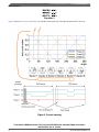
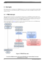
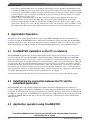
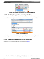
Freescale Semiconductor
Application Note
Document Number: AN5049
Rev. 0, 12/2014
Three-Phase PMSM Sensorless
FOC Using the MKV10Z32 with
Automated Motor Parameters
Identification
by:
Josef Tkadlec
Contents
1 Introduction
This application note accompanies the Sensorless PMSM
Field-Oriented Control Design Reference Manual (DRM148)
[1]. This application note describes the MCU peripherals used
in the PMSM sensorless vector control application, the
hardware set-up, and results of the measurement.
In addition, the attached application code contains routines for
Automated PMSM parameters identification.
2 MCU Peripherals
Table 1 summarizes the peripherals on the Kinetis
MKV10Z32 MCU [4] and their usage by the PMSM
sensorless vector control application.
© 2014 Freescale Semiconductor, Inc.
1
Introduction.............................. .............................. 1
2
MCU Peripherals..................................................... 1
3
Interrupts.............................. ................................... 8
4
Application Operation................. ..........................10
5
Project File Structure..................... ....................... 14
6
Memory Usage.......................... ............................16
7
Hardware Setup.....................................................16
8
Measurement Results............................................ 18
9
Conclusion.............................................................19
10
References............................. ................................19
11
Acronyms and Abbreviated Terms.... ...................19
MCU Peripherals
Table 1. Kinetis KV10Z32 Peripherals Overview
Kinetis KV10 peripherals
Group
Analog
Communications
Timers
Other
Module
Used in the
application
Number of modules
or channels
Purpose
ADC0
11 channels single
ended, 2 of them
differential pairs
2 channels
DC-bus voltage and
motor phase currents
sensing
ADC1
11 channels single
ended, 2 of them
differential pairs
3 channels
Comparators
2 modules, each 7
channels
—
—
DAC
1 module
—
—
SPI
1 module, 4 chip select 1 module
signals
MOSFET driver
configuration
UART
2 modules
1 module
FreeMASTER
communication
I2C
1
—
—
FlexTimer
6 channels
6 channels
Generation 6-channels
PWM for motor control
2 channels
1 channel
Generation of slow loop
interrupt
2 channels
—
—
PDB
8 channels for ADC
triggering
2 channels
DC-bus voltage and
phase current sampling
initiation
LPT
1 module
—
—
eDMA
4 channels
—
—
2.1 FlexTimer0 configuration to generate a 6-channel PWM
The FlexTimer Module (FTM) is a two to eight channel timer which supports input capture, output compare, and the
generation of PWM signals to control an electric motor and power management applications. The FTM time reference is a
16-bit counter that can be used as an unsigned or signed counter. On the Kinetis KV10 MCUs there are three instances of
FTM. One FTM has 6 channels, the other two FTMs have 2 channels.
The FTM0 is clocked from the system clock (75 MHz), and the generated PWM has a frequency of 20 kHz (period 50 us),
therefore MODULO must be 3750 (CNTIN register –1875, MOD1 1874). There is an interrupt generated every second PWM
reload by FTM0 (period 100 us = 10 kHz). This interrupt serves to calculate fast loop (Current FOC) algorithms. The
procedure of the FlexTimer configuration for generating a center-aligned PWM with dead time insertion is described in [2].
Because [2] supports an earlier version (1.0) of the FlexTimer, and with regards to the hardware used (TWR-MC-LV3PH),
there are a few differences in the configuration, as follows:
• It is necessary to enable the system clock for the FlexTimer module in the Clock Gating Control register:
SIM→SCGC6 |= SIM_SCGC6_FTM0_MASK;
• It is necessary to disable the write protection of some registers before they can be updated:
Three-Phase PMSM Sensorless FOC Using the MKV10Z32 with Automated Motor Parameters
Identification, Rev. 0, 12/2014
2
Freescale Semiconductor, Inc.
MCU Peripherals
FTM0→MODE |= FTM_MODE_WPDIS_MASK;
• It is recommended to enable the internal FlexTimer counter to run in the debug mode:
FTM0→CONF |= FTM_CONF_BDMMODE(3);
• When the HW debugging interface (jLink, Multilink,…) is connected to the microcontroller, the MCU is in debug
mode. This is not dependent on running code containing breakpoints.
• The PWM signals generated by the FlexTimer0 are directly connected to the MOSFET driver. Because of safety
reasons, the input signals for the top transistors on the MOSFET driver used on the Freescale Tower System
development board low-voltage power stage have inverse polarity. Therefore, it is also necessary to set the right
polarity of the PWM signals:
FTM0→POL = FTM_POL_POL0_MASK |
FTM_POL_POL2_MASK |
FTM_POL_POL4_MASK;
• The duty cycle is changed by changing the value of the FlexTimer Value registers. These registers are double-buffered,
meaning that their values are updated not only by writing the number, but also by confirming the change by setting the
Load Enable (LDOK) bit. This ensures that all values are updated at the same instance:
FTM0→PWMLOAD = FTM_PWMLOAD_LDOK_MASK;
It is necessary to write the LDOK bit every time the value registers are changed, so not only at the stage of loading
them with initial values, but with every update after the duty cycle value is computed in the vector control algorithm.
• Within the application, hardware triggering of the AD converter is employed. The Initialization Trigger signal from the
FlexTimer is used as the primary triggering signal which is fed into the Programmable Delay Block that services the
timing of the AD conversion initiation.
FTM0→EXTTRIG |= FTM_EXTTRIG_INITTRIGEN_MASK;
• FTM0 interrupt is generated on every second PWM reload:
FTM0->SC |= FTM_SC_TOIE_MASK;
FTM0->CONF |= FTM_CONF_NUMTOF(1);
• Finally, the output pins of the MCU must be configured, to bring out the signals from the chip. The assignment of
signals to output pins is set in the Pin Control Register. The available signals are listed in the Signal Multiplexing
chapter of [3] and are package dependent.
PORTC->PCR[1] = PORT_PCR_MUX(4); // FTM0 CH0
PORTE->PCR[25] = PORT_PCR_MUX(3); // FTM0 CH1
PORTC->PCR[3] = PORT_PCR_MUX(4); // FTM0 CH2
PORTC->PCR[4] = PORT_PCR_MUX(4); // FTM0 CH3
PORTD->PCR[4] = PORT_PCR_MUX(4); // FTM0 CH4
PORTD->PCR[5] = PORT_PCR_MUX(4); // FTM0 CH5
The port settings implemented in the application code reflect the hardware solution built on the Tower System development
modules.
2.2 FlexTimer2 configuration to generate a slow loop interrupt
Three-Phase PMSM Sensorless FOC Using the MKV10Z32 with Automated Motor Parameters
Identification, Rev. 0, 12/2014
Freescale Semiconductor, Inc.
3
MCU Peripherals
The Flex Timer Module 2 (FTM2) is configured to generate an independent interrupt that serves to calculate slow loop
(Speed FOC) algorithms. The slow loop interrupt is processed with lower priority than the fast loop interrupt. Separation of
the slow and fast state machine shortens the necessary length of the fast loop interrupt. Prescale factor (FTM2_SC -> PS) is
16 and modulo register (FTM2_MOD) is set to 75000/16 therefore FTM2 counter overflows and generates the slow loop
interrupt with frequency 1kHz.
2.3 ADC and PDB modules configuration
The on-chip ADC module is used to sample feedback signals (motor phase currents and DC-bus voltage) that are necessary
to successfully perform the vector control algorithm. The Programmable Delay Block closely cooperates with the ADC and
triggers the hardware for sampling.
It is required to perform a self-calibrating procedure of the ADC module before it is used in the application to obtain the
specified accuracy. The calibration process also requires a programmer’s intervention—that is, to generate the plus-side and
minus-side gain calibration results and store them in the ADC plus-side and minus-side gain registers after the calibration
function completes. The calibration must be performed for both ADC modules. After calibration, the ADC modules are
configured to a 12-bit accuracy. The CPU frequency is set to 75 MHz, so by using available prescaler values the input clock
to the ADC module is set to 12.5 MHz. That setting yields a conversion time of 2.64 μs (33 ADC clock cycles). Finally, the
hardware trigger must be enabled in the Status and Control Register 2.
The Programmable Delay Block (PDB) provides controllable delays from either an internal or an external trigger, or a
programmable interval tick, to the hardware trigger inputs of the ADCs, so that a precise timing between ADC conversions is
achieved. The PDB module has an internal counter that overflows on a modulo value. Because the input trigger periodically
comes from FTM0, the value of the modulo register can be set to its reset value. The values in the channel delay registers are
set to generate triggers to start sampling the DC-bus voltage and the motor phase AD conversions. The PDB module on the
KV10 MCU allows 15 different input trigger sources. They are listed in the Chip configuration chapter, in section PDB
Configuration in [4]. Similarly, as for FTM0, the LDOK bit must be set to acknowledge the changes in the delay registers.
On the KV10 MCU the clock source for the PDB is different than the FTM—that is, the PDB and the ADC use the Bus
Clock and the FTM uses the System Clock.
2.4 ADC conversion timing, currents and voltage sampling
FlexTimer0 is configured to trigger an internal hardware signal when its counter is reset after overflow to the initialization
value. This signal is fed into the Programmable Delay Block (PDB) that consequently triggers the AD conversion of the
voltage and currents with a predefined delay. On the Kinetis KV10 75 MHz MCU, two ADC modules are implemented. Each
ADC module associates to one channel of the PDB module. Each ADC module has two result registers (two channels), and
they correspond to two programmable pre-trigger delays of the PDB channels. So it is possible to perform four AD
conversions without requesting an interrupt (with respect that the DMA is not used for data transfer). In this application, only
three conversions need to be triggered without CPU intervention (two motor phase currents and the DC-Bus voltage). Figure
1 shows the module interconnections and the ADC interrupt generation.
Three-Phase PMSM Sensorless FOC Using the MKV10Z32 with Automated Motor Parameters
Identification, Rev. 0, 12/2014
4
Freescale Semiconductor, Inc.
MCU Peripherals
Figure 1. ADC conversion timing diagram
2.5 Current measurement
Closely related to the ADC conversion trigger timing is the assignment of the ADC channels to the measured analog signals.
For computation of the fast (current) control loop of the FOC, it is necessary to know the values of all three motor phase
currents. Because there are only two ADC modules, it is possible to sample only two analog quantities in one instance.
Assuming the motor represents a symmetrical three-phase system, the sum of all three instantaneous phase currents is zero.
Equation 1
Because the phase currents are measured the instance when the bottom transistors are conducting, in the case of high duty
cycle ratios (current value is in the area of the maximum of the sine curve), the time when the current can be measured is too
short. The bottom transistor must be switched on at least for a critical pulse width to get a stabilized current shunt resistor
voltage drop. The selection of the channels is determined based on the section when the space vector of the stator current is
generated. This assignment is performed at the end of the ADC1 interrupt service routine. Therefore, it is enough to sample
only two phase currents while the third is easily calculated according to Equation 2 on page 6.
Three-Phase PMSM Sensorless FOC Using the MKV10Z32 with Automated Motor Parameters
Identification, Rev. 0, 12/2014
Freescale Semiconductor, Inc.
5
MCU Peripherals
Equation 2
Figure 2 illustrates two cases (case I at 30°, case II at 60°) which explain why calculating the third current is necessary.
Figure 2. Current sensing
Three-Phase PMSM Sensorless FOC Using the MKV10Z32 with Automated Motor Parameters
Identification, Rev. 0, 12/2014
6
Freescale Semiconductor, Inc.
MCU Peripherals
2.6 Overcurrent level
The overcurrent signal is connected via the TWR-Elevator IRQ_A (B62) pin to the GPIO_B2 pin of the MKV10Z32 device.
This pin is internally connected to the FTM0_FLT1 signal that handles the fault by PWM hardware. See Figure 3.
The overcurrent level can be set in the range of 0~8 A by the trimmer R37 on the TWR-MC-LV3PH board. The maximum
current level can be set by turning the trimmer counterclockwise. The user can find the level by turning the trimmer
counterclockwise while the motor is running until the red LED is lit. It is recommended to set the trimmer to a somewhat
higher level, so that the motor can operate at maximum speed.
Figure 3. Overcurrent level
2.7 SPI configuration
The SPI interface is used in the application for communication between the intelligent MOSFET gate driver MC33937 and
the KV10 MCU. The MC33937 gate driver is placed on the Tower System low-voltage power module and serves for driving
the high-side and low-side MOSFET transistors of the three-phase inverter. In the application, the initialization of the
MC33937 must be performed, primarily to set dead time. During the motor operation there is also periodic checking of the
status register of the driver, to provide information on the latched faults. The MC33937 driver requires precise timing of the
SPI signals. The default setting of the SPI module on the MCU is not possible to use. The exact timing of the SPI signals is
listed in [5].
2.8 SCI (UART) configuration
The SCI is used in the application for the communication between the master system and the embedded application. A master
system is the notebook or the PC where the FreeMASTER software is installed to control the application and visualization of
its state. On the Kinetis KV10, there are two UART modules implemented. Because the hardware solution is based on the
Tower System development boards, the UART1 is used. The communication speed is set to 19200 Bd and is limited by use
of the OpenSDA - CDC serial communication driver. The use of direct RS232 connection between the PC and the embedded
side enables an increase of the communication speed to 115200 Bd.
Three-Phase PMSM Sensorless FOC Using the MKV10Z32 with Automated Motor Parameters
Identification, Rev. 0, 12/2014
Freescale Semiconductor, Inc.
7
Interrupts
3 Interrupts
In the application there are 4 interrupts in total. FTM0 interrupt serves to execute fast loop (Current FOC) algorithms, FTM2
serves to execute slow loop (Speed FOC) algorithms, ports interrupt handles user buttons and PDB error interrupt clears the
sequence error fault.
3.1 FTM0 interrupt
This interrupt request executes fast loop state machine and is triggered every second PWM reload. In the beginning of the
FTM0 ISR execution an application state machine function is called. If the application is in the Run state, then it is followed
by the execution of the fast (current) control loop of the PMSM vector control algorithm, including the position and speed
estimation. The interrupt flag is cleared by writing 0 to TOF bit in FTM0->SC register.
The flow chart depicted on the Figure 4 provides an overview of the program flow during execution of the FTM0 interrupt
service routine when the application is in Run state and Spin sub-state.
Figure 4. FTM0 ISR flow chart
Three-Phase PMSM Sensorless FOC Using the MKV10Z32 with Automated Motor Parameters
Identification, Rev. 0, 12/2014
8
Freescale Semiconductor, Inc.
Interrupts
3.2 FTM2 interrupt
This interrupt request executes slow loop state machine and is triggered when FTM2 overflows therefore it is independent on
FTM0 interrupt. Speed control functions are called in this interrupt. The interrupt flag is cleared by writing 0 to TOF bit in
FTM2->SC register.
The flow chart depicted in Figure 5 provides an overview of the program flow during execution of the FTM2 interrupt
service routine when the application is in the Run state and the Spin sub-state.
Figure 5. FTM2 ISR flow chart
3.3 Ports interrupt
Handling of the user’s button on the Kinetis KV10 MCU Tower System controller board is performed in the ISR associated
with the Ports interrupt, generated whenever the SW2 button is pressed. At the beginning, the interrupt flag is cleared.
Pressing the SW2 button enables/disables the Demo mode. The first pressing of the SW2 button puts the application state into
RUN mode and the required speed is changed in several steps according to a predefined profile. The subsequent press of the
SW2 button returns the application to STOP mode.
More about the application control is available in Application Operation. Using the FreeMASTER control interface enables
enhanced control and diagnostic.
3.4 PDB error interrupt
The PDB error ISR serves to clear the sequence error fault that is generated in situations when PDB initiates the sampling of
the AD converter even though the COCO flag in the specific ADCx_SC1n register of the ADC module was not cleared. The
values from the result registers are not read, due to the reasons described as follows.
Three-Phase PMSM Sensorless FOC Using the MKV10Z32 with Automated Motor Parameters
Identification, Rev. 0, 12/2014
Freescale Semiconductor, Inc.
9
Application Operation
• One scenario is when the PDB counter stops working and an interrupt is asserted. The ISR in the PDB module is then
re-initiated. The PDB generates a trigger signal with the same period as the ADC conversion complete interrupt which
is also the same as the PWM period. If the user places an interrupt in the code, this stops execution. However, the PDB
generates a trigger for the next conversion, even when the program execution stops. The COCO flags are not cleared
and the PDB generates a sequence error.
• Another scenario is when the execution of the ADC conversion complete interrupt (when the fast control loop is
calculated) extends over one period of the PWM. This occurs if the user enters additional tasks into the ADC
conversion complete interrupt. In addition to the generation of PDB sequence error, the more serious impact is on the
quality of the control process, as one of the key assumptions is not met—the execution of control algorithms to extend
the sampling period. The real-time control application must be designed in such a way that this situation never occurs.
4 Application Operation
The application can be operated either with the user button on the TWR-KV10Z32 MCU board (as mentioned in Ports
interrupt) or by using the FreeMASTER software, which enables visualizing the application variables. The FreeMASTER
application consists of two parts, the PC application used for variables visualization, and the set of software drivers running
in the embedded application. The data between the PC and the embedded application is passed via the RS232 interface.
4.1 FreeMASTER installation on the PC or notebook
The FreeMASTER PC application can be downloaded from the Freescale webpage: http://www.freescale.com/freemaster;
from the “Download” tab, select “FreeMASTER 1.4 Application Installation”. Because downloading the FreeMASTER
application requires registration, it is necessary to create an account before you can log-in. After you log into the system, the
license agreement appears. You should read the license agreement and then you have to accept the agreement by clicking the
“I Accept” button. If you are using Internet Explorer, then at the top of the web page you will see a bar asking to authorize
the file download. Click on the bar and select "Download File". A dialog box appears where you can choose to either Run or
Save. In both cases, the installation archive will be stored on your machine. By selecting the “Save”, you have the option to
select your preferred location for saving the installation archive, otherwise it will be saved to a Temporary folder created by
your system. The library installation archive will be now downloaded to your computer.
To run the installation, click the “Run” button. Follow the instructions on the screen to complete the installation process.
4.2 Establishing the connection between the PC and the
embedded application
The FreeMASTER allows using multiple communication interfaces between the embedded application and the PC or
notebook (UART (RS232), CAN, Ethernet, USB, BDM, etc). For this application, the RS232 was used because the software
overhead for the data transfer represents the lowest additional load on the CPU. Nowadays, notebooks are not equipped with
the COM port, so for this purpose the TWR-KV10Z32 module has in place a USB-to-RS232 interface (CDC Serial Port). By
connecting the TWR-KV10Z32 module with a notebook via the USB cable, a virtual serial port will be established in the
Windows system.
4.3 Application operation using FreeMASTER
Three-Phase PMSM Sensorless FOC Using the MKV10Z32 with Automated Motor Parameters
Identification, Rev. 0, 12/2014
10
Freescale Semiconductor, Inc.
Application Operation
To run the FreeMASTER application, double click on the PMSM_FOC_KV1x.pmp file located in the \freemaster
\PMSM_Sensorless_FOC_MID folder. The FreeMASTER application starts and the environment will be automatically
created, as it is defined in the *.pmp file.
4.3.1 Setting up the communication
When the notebook is connected via USB cable with the TWR-KV10Z32 board, the operating system assigns the number of
the COM port to the OpenSDA CDC Serial Port. This number is assigned randomly, therefore it is necessary to set the right
communication port each time the connection is established (re-plugging the USB cable might cause a different port number
assignment).
To set the port number, click the menu item Project \ Options …
Then assign the port number in the “Comm” tab of the opened window.The correct port number selection is confirmed by
the text “OpenSDA – CDC Serial Port” next to the list box with the available serial port numbers.
Figure 6. FreeMASTER communication settings
4.3.2 Application operation
4.3.2.1
Start/Stop the communication
When the communication settings are performed, the communication between the PC and the embedded application can be
initiated. Click the STOP button in the FreeMASTER toolbar as shown in following picture:
Three-Phase PMSM Sensorless FOC Using the MKV10Z32 with Automated Motor Parameters
Identification, Rev. 0, 12/2014
Freescale Semiconductor, Inc.
11
Application Operation
Figure 7. Initiating the communication with the embedded side
4.3.2.2
Start/Stop the application, required speed setting
The next step is to switch the application to the RUN state. In the FreeMASTER window in the Variable Watch grid, click on
the drop-down list next to the “Application Switch” variable name, and select “ON” as the following picture illustrates:
Figure 8. Start the application
Once the application is set to the RUN state, the required speed can be changed to some non-zero value. The procedure is
similar as in the previous step; in the Variable Watch grid, enter a positive or negative value next to the “Speed Required”
variable name.
4.3.2.3
Operation of the application from the control page
The application can also be operated from the control page, see the description in Figure 9.
Three-Phase PMSM Sensorless FOC Using the MKV10Z32 with Automated Motor Parameters
Identification, Rev. 0, 12/2014
12
Freescale Semiconductor, Inc.
Application Operation
Figure 9. FreeMASTER control page
4.3.2.4
Scopes and Recorders
One of the main benefits of the FreeMASTER application is to visualize the values of the variables in real time. For this
purpose, there are two possibilities. The user can select between the Scope and the Recorder. While the Scope feature
downloads a stream of the data continuously in real time, the Recorder stores the data in a buffer located in the RAM of the
embedded MCU and, after a trigger condition is met, the data is transferred in blocks via the communication interface and
visualized in the FreeMASTER window. The sampling period of the Scope is limited by the speed of the communication
interface, and therefore is used for slowly changing quantities such as the speed. The sampling period of the oscilloscope-like
Recorder is in the microseconds range, enabling visualization of quickly changing quantities, such as the phase currents or
the duty cycles. In this application, the recorder buffer is updated each time the fast control loop is executed, that is, every
100 us.
The following picture shows the Recorders and Scopes that can be used when the application is running in the “Speed FOC”
control mode.
Three-Phase PMSM Sensorless FOC Using the MKV10Z32 with Automated Motor Parameters
Identification, Rev. 0, 12/2014
Freescale Semiconductor, Inc.
13
Project File Structure
Figure 10. Scopes and recorders used in Speed FOC control mode
4.4 MCAT tool control
To run the FreeMASTER application including MCAT tool, double click on the MCAT_PMSM_FOC_KV1x.pmp file
located in the \freemaster\PMSM_Sensorless_FOC_MID folder. The FreeMASTER application starts and the environment
will be automatically created, as it is defined in the *.pmp file.
The application enables tuning of the PMSM sensorless application to any motor. For this purpose, the field oriented control
can be divided into four modes as follows:
•
•
•
•
Scalar
Voltage FOC
Current FOC
Speed FOC
This enables tuning of the application during several steps, with each step containing a limited number of unknown
parameters that can be adjusted. To switch between these modes, an MCAT tab “Control Struc” is used. For more
information on tuning the application to any motor, see [6].
4.4.1 Automated PMSM parameters identification
The application code contains routines for a PM synchronous motor parameters identification. The algorithm simplifies and
speeds up controller constant calculations and settings. The identification process is disabled by default in the application and
can be enabled from the MCAT control tab “Motor Identif”. For more information on user motor identification, see Freescale
document AN4986, “Automated PMSM Parameter Identification” [7].
5 Project File Structure
The total number of source (*.c) and header files (*.h) in this project exceeds one hundred. Therefore, only the key project
files will be described in detail, and the remainder will be summarized in groups.
Three-Phase PMSM Sensorless FOC Using the MKV10Z32 with Automated Motor Parameters
Identification, Rev. 0, 12/2014
14
Freescale Semiconductor, Inc.
Project File Structure
The main project folder is divided into three directories:
• build\iar\kv10\PMSM_Sensorless—contains the configuration files for the IAR compiler as well as the compiler’s
output executable and object files. If the IAR Embedded Workbench for ARM is installed on your computer, double
clicking the workspace file PMSM_SAC_SENSORLESS.eww located in the directory \build\iar\ launches the IAR
IDE.
• freemaster\PMSM_Sensorless—contains the FreeMASTER configuration file PMSM_FOC_KV1x.pmp and
supporting files (control page in HTML format and the binary file with addresses of the variables).
It also contains the FreeMASTER project for the Motor Control Application Tuning Tool
PMSM_FOC_KV1x_MCAT.pmp.
• src—contains the project source and header files, and its contents will be described in the following text:
Files in the src\projects\kv10\PMSM_Sensorless_FOC folder:
• main.c and main.h contain the basic application initialization (enabling interrupts), subroutines to access the
MCU peripherals, and interrupt service routines. In the background infinite loop the FreeMASTER
communication is performed.
• state_machine.c and state_machine.h contain the application state machine structure definition and handles the
switching between the application states and application states’ transitions.
• motor_structure.c and motor_structure.h contain the structure definitions and subroutines dedicated to
perform the motor control algorithm (vector control algorithm, position and speed estimation algorithm, speed
control loop).
• M1_statemachine.c and M1_statemachine.h contain the software routines that are executed when the
application is in the particular state or state transition.
• freemaster_cfg.h configuration file for the FreeMASTER interface.
• PMSM_appconfig.h contains the constant definitions of the application control processes (parameters of the
motor and controllers and the constants for other vector control related algorithms). When the application is
tailored for another motor using the Motor Control Application Tuning Tool, this file is generated by the tool at
the end of the tuning process.
• \peripherals\ folder contains the important files for static configuration of the peripherals used in the application
(FlexTimers, ADC, PDB, SPI).
Subdirectories in the src\ folder:
• \common\ and \cpu\ folders containing CPU initialization routines.
• \cpu\isr.h an important file with definitions of the peripherals interrupt service routines assigned to the interrupt
vectors. In this file, the user can add the definition of an ISR for an additional peripheral interrupt.
• \drivers\ files in the subdirectories contain generic source and header files for UART and watchdog
configuration, as well as the CPU clock settings routines.
• \platforms\tower.h contains the Tower System development board definitions for Kinetis (CPU speed and
UART parameters).
• \platforms\MKV10Z7.h is the header file containing macro definitions of all the MCU registers and register
bits.
Files in the src\MMCLIB\ folder:
• CM0+_MMCLIB_IAR.a software library containing motor control, general math and filter algorithms.
Additional files in the folder and subfolders are associated header files, each one for a particular function of the
library.
• ACLIB\CM0+_ACLIB_IAR_r0.2.a contains the advanced control algorithms for rotor position and speed
estimation (Back-EMF observer and Tracking observer).
Other subdirectories in the src\ folders:
Three-Phase PMSM Sensorless FOC Using the MKV10Z32 with Automated Motor Parameters
Identification, Rev. 0, 12/2014
Freescale Semiconductor, Inc.
15
Memory Usage
• \FreeMASTER contains all source files of the FreeMASTER application, it is not necessary to access it or
change anything inside. The interface to the programmer is only via freemaster_cfg.h file located in src\projects
\kv10\PMSM_Sensorless folder.
• \SAC\ folder (Sensor and Actuator Components) contains routines to access peripherals used by the motor
control algorithm to sense input feedback physical quantities (currents, voltage, speed, position) and to set the
actuators based on calculated output variables (FlexTimer, MOSFET pre-driver).
6 Memory Usage
Table 2 summarizes the chip memories usage:
Table 2. Total Memory Usage
Memory Type
Total Memory Available on the
Kinetis MKV10Z32
Used by the Application [ Bytes ]
32KB
22,970
Program Flash (application code)
Data Flash (application constants)
1,650
Data RAM (application variables)
8KB
6,6141
1. Including 4096 bytes of FreeMASTER recorder buffer.
Table 3 summarizes the chip memories usage for selected algorithm blocks:
Table 3. Algorithm Blocks Memory Usage
Algorithm Block
Program Memory (Code + Constants)
Data Memory
[ Bytes ]
[ Bytes ]
FOC (fast + slow loops)
5,114
0
FreeMASTER
2,572
4,305
SAC (Sensor and Actuator Components)
2,974
3
MID (Motor Identification)
4,252
590
Application State Machine
4,764
676
7 Hardware Setup
The Tower System development board platform is used as the hardware platform for the PMSM sensorless on Kinetis
MKV10Z32. It consists of the following modules:
• Tower System elevator modules (TWR-ELEV)
• Kinetis MKV10Z32 Tower System module (TWR-KV10Z32)
• Three-phase low-voltage power module (TWR-MC-LV3PH) with included motor
All modules of the Tower System development platform are available for order via the Freescale web page or from
distributors, so the user can easily build the hardware platform for which the application is targeted.
Three-Phase PMSM Sensorless FOC Using the MKV10Z32 with Automated Motor Parameters
Identification, Rev. 0, 12/2014
16
Freescale Semiconductor, Inc.
Hardware Setup
7.1 Hardware set-up and jumpers configuration
Building the system using the modules of the Tower System is not difficult. The peripheral modules and the MCU module
are plugged into the elevator connectors, while the white stripe on the side of the module boards determines the orientation to
the Functional elevator (the elevator with the mini USB connector, power supplies and the switch).
It is necessary to configure jumpers on both the TWR-KV10Z32 module and the TWR-MC-LV3PH module. The jumper
settings for TWR-KV10Z32 board are listed and highlighted in the following table.
Table 4. Jumper Settings of TWR-KV10Z32 Board
Jumper #
Setting
Jumper #
Setting
J1
2-3
J14
open
J2
1-2
J18
2-3
J3
2-3
J19
2-3
J4
1-2
J20
2-3
J5
1-2
J21
3-4
J7
1-2
J22
3-4
J8
2-3
J25
open
J9
1-2
J26
1-2
J10
2-3
J27
1-2
J11
open
J28
1-2
J12
open
J29
1-2
J13
open
Three-Phase PMSM Sensorless FOC Using the MKV10Z32 with Automated Motor Parameters
Identification, Rev. 0, 12/2014
Freescale Semiconductor, Inc.
17
Measurement Results
The jumper settings for TWR-MC-LV3PH board are listed and highlighted in the following table. See also the user’s manual
[7] for more details (for example the hardware overcurrent threshold setting) of the TWR-MC-LV3PH stage.
Table 5. Jumper Settings of TWR-MC-LV3PH Board
Jumper #
Setting
J2
1-2
J3
1-2
J10
1-2
J11
1-2
J12
1-2
J13
1-2
J14
1-2
8 Measurement Results
8.1 CPU load and the execution time
The CPU load is influenced mainly by the execution of the FTM0 ISR, in which the execution of the application state
machine and calculation of the fast (current) control loop of the PMSM vector control is performed.
Table 6 shows machine cycle number measured from FTM0 ISR routine excluding FreeMASTER recorder function in RUN
state for the worst case of RUN STATE—that is, a transition from open loop startup to close loop speed control.
The FTM0 interrupt is generated periodically with a half frequency as the PWM reload event, when the values of the duty
cycles are updated.
In this application, the FTM0 ISR is generated once per 100μs, which corresponds to 10 kHz (20 kHz PWM frequency). At
75MHz on the Kinetis MKV10Z32 device, it consumes up to 72% of CPU performance.
Table 6. CPU Load (CPU Clock 75 MHz)
Algorithm Block
FOC + open loop start-up
CPU Cycles
Execution Time
[usec]
Note
5,418
72.2
RUN state worst case
Three-Phase PMSM Sensorless FOC Using the MKV10Z32 with Automated Motor Parameters
Identification, Rev. 0, 12/2014
18
Freescale Semiconductor, Inc.
Conclusion
9 Conclusion
The results of the execution time measurement show that the Kinetis MKV10Z32 microcontroller can be used to drive the
PMSM sensorless vector control algorithm for high dynamic applications. The CPU load at 10 kHz FOC calculation
frequency is about 72 %, so there is much room to either to increase the frequency of the fast control loop or to perform
additional user’s tasks.
10 References
The following references are available on http://www.freescale.com with the exception of [3]:
[1] Sensorless PMSM Field-Oriented Control (Document number DRM148)
[2] Using FlexTimer in ACIM/PMSM Motor Control Applications (Document number AN3729)
[3] A New Starting Method of BLDC Motors Without Position Sensor, Wook-Jin Lee, Seung-Ki Sul, 2006
[4] KV10 Sub-Family Reference Manual (Document number KV10P48M75RM)
[5] Three Phase Field Effect Transistor Pre-driver Data Sheet (Document number MC33937)
[6] Tuning 3- Phase PMSM Sensorless Control Application Using MCAT Tool (Document number AN4912)
[7] Automated PMSM Parameters Identification (Document number AN4986)
[8] TWR-MC-LV3PH User’s Manual (Document number TWRMCLV3PHUG)
11 Acronyms and Abbreviated Terms
Table 7 contains abbreviated terms used in this document.
Table 7. Acronyms and Abbreviated Terms
Term
Meaning
ADC
Analog to Digital Converter
Back-EMF
Back electromotive force – a voltage generated by rotating
motor
PMSM
Permanent Magnet Synchronous Motor
PWM
Pulse-Width Modulation
Three-Phase PMSM Sensorless FOC Using the MKV10Z32 with Automated Motor Parameters
Identification, Rev. 0, 12/2014
Freescale Semiconductor, Inc.
19
How to Reach Us:
Home Page:
freescale.com
Web Support:
freescale.com/support
Information in this document is provided solely to enable system and
software implementers to use Freescale products. There are no express
or implied copyright licenses granted hereunder to design or fabricate
any integrated circuits based on the information in this document.
Freescale reserves the right to make changes without further notice to
any products herein.
Freescale makes no warranty, representation, or guarantee regarding
the suitability of its products for any particular purpose, nor does
Freescale assume any liability arising out of the application or use of
any product or circuit, and specifically disclaims any and all liability,
including without limitation consequential or incidental damages.
“Typical” parameters that may be provided in Freescale data sheets
and/or specifications can and do vary in different applications, and
actual performance may vary over time. All operating parameters,
including “typicals,” must be validated for each customer application by
customer's technical experts. Freescale does not convey any license
under its patent rights nor the rights of others. Freescale sells products
pursuant to standard terms and conditions of sale, which can be found
at the following address: freescale.com/SalesTermsandConditions.
Freescale, the Freescale logo, and Kinetis are trademarks of Freescale
Semiconductor, Inc., Reg. U.S. Pat. & Tm. Off. Tower is a trademark of
Freescale Semiconductor, Inc. All other product or service names are
the property of their respective owners. ARM and the ARM Powered
logo are registered trademarks of ARM Limited (or its subsidiaries) in
the EU and/or elsewhere.
© 2014 Freescale Semiconductor, Inc.
Document Number AN5049
Revision 0, 12/2014