1
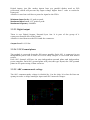
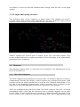
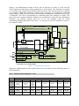
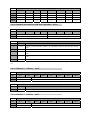
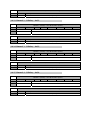
Unit / Module Description:
Twelve 16-bit ADC module (10 MSPS)
Unit / Module Number:
SMT916
Document Issue Number:
1.1
Issue Date:
08/07/2011
Original Author:
Philippe Robert
User Manual
for
SMT916
Sundance Multiprocessor Technology Ltd, Chiltern House,
Waterside, Chesham, Bucks. HP5 1PS.
This document is the property of Sundance and may not be copied
nor communicated to a third party without prior written
permission.
© Sundance Multiprocessor Technology Limited 2009
Revision History
Issue
Changes Made
Date
Initials
1
Original document released
06/07/2011
PhSR
1.1
Ordering information added
08/07/2011
PhSR
Table of Contents
1 2 Introduction ................................................................................................................... 6 Related Documents....................................................................................................... 7 2.1 Referenced Documents .............................................................................................. 7 2.2 Applicable Documents ............................................................................................... 7 3 Functional Description ................................................................................................ 7 3.1 Block Diagram.............................................................................................................. 7 3.2 Module Description .................................................................................................... 8 3.3 Interface Description.................................................................................................. 8 3.3.1 Mechanical Interface .............................................................................................. 8 3.3.2 Electrical Interface ................................................................................................. 8 3.3.2.1 Analogue inputs ............................................................................................ 8 3.3.2.2 Digital Inputs ................................................................................................. 8 3.3.2.3 Digital output ................................................................................................ 9 3.3.2.4 VCC/Ground planes ..................................................................................... 9 3.3.2.5 ADC common mode voltage ....................................................................... 9 3.3.2.6 Input dual opamp structure ..................................................................... 10 3.4 Firmware ..................................................................................................................... 10 3.4.1 FPGA Block Diagram. ........................................................................................... 10 3.4.2 Global Control Register – 0x4 ............................................................................ 11 3.4.3 Global Status Register – 0x4 .............................................................................. 13 3.4.4 Conversion rate register channels 0 to 5 – 0x10. .......................................... 14 3.4.5 Conversion rate register channels 6 to 11 – 0x11. ........................................ 15 3.4.6 Storage Control Register – 0x12 ........................................................................ 15 3.4.7 ADCs Output Format GroupA – 0x13 .............................................................. 17 3.4.8 ADCs Output Format GroupB – 0x14 ............................................................... 17 3.4.9 Led Register – 0x15 .............................................................................................. 17 3.4.10 Channel Selection for read back operation – 0x20. ....................................... 18 3.4.11 Channel 0 – IODelay – 0x30. .............................................................................. 18 3.4.12 Channel 1 – IODelay – 0x31. .............................................................................. 18 3.4.13 Channel 2 – IODelay – 0x32. .............................................................................. 19 3.4.14 Channel 3 – IODelay – 0x33. .............................................................................. 19 3.4.15 Channel 4 – IODelay – 0x34. .............................................................................. 19 3.4.16 Channel 5 – IODelay – 0x35. .............................................................................. 20 3.4.17 Channel 6 – IODelay – 0x36. .............................................................................. 20 3.4.18 Channel 7 – IODelay – 0x37. .............................................................................. 20 3.4.19 Channel 8 – IODelay – 0x38. .............................................................................. 20 3.4.20 Channel 9 – IODelay – 0x39. .............................................................................. 21 3.4.21 Channel 10 – IODelay – 0x3A. ............................................................................ 21 3.4.22 Channel 11 – IODelay – 0x3B. ............................................................................ 21 4 Verification Procedures ............................................................................................. 22 Power Consumption – Heat dissipation. ................................................................ 22 5 5.1 AD7626 ADC Chip. ................................................................................................... 22 5.2 Linear regulators. ...................................................................................................... 22 5.3 Clock distribution chips. ......................................................................................... 23 5.4 Power consumption .................................................................................................. 23 6 PCB Layout ................................................................................................................... 23 6.1 ADC Channel .............................................................................................................. 23 6.2 Top Layer .................................................................................................................... 25 6.3 Bottom Layer .............................................................................................................. 25 7 Performance ................................................................................................................. 26 7.1 DC Input – 10MSPS. .................................................................................................. 26 8 Pinout ............................................................................................................................ 27 9 Physical Properties ..................................................................................................... 27 10 Safety ............................................................................................................................. 28 11 Cooling .......................................................................................................................... 28 12 EMC ................................................................................................................................ 28 13 Ordering Information ................................................................................................. 28 Table of Figures
Figure 1 – SMT916 Block Diagram. ........................................................................................ 7 Figure 2 - ADCs common mode voltage. .............................................................................. 9 Figure 3 - ADCs input front-end. .......................................................................................... 10 Figure 4 - Firmware Block Diagram...................................................................................... 11 Figure 5 - ADC Channel Layout. ........................................................................................... 24 Figure 6 - Top Layout. ............................................................................................................. 25 Figure 7 - Bottom Layout........................................................................................................ 25 Figure 8 – DC Input distribution - 4k samples - 10MSPS. ................................................ 26 Figure 9 – DC Input - Time domain - 10MSPS. ................................................................... 26 Figure 10 – DC Input - Frequency domain - 10MSPS. ....................................................... 27 Figure 11 - DC Input - Distribution of all 12 channels..................................................... 27 1 Introduction
The SMT916 is an SLB mezzanine board that incorporates twelve AD7626 ADC chips
from Analog Devices (Two groups of six ADCs, Group A for the first six channels
and Group B for the next six channels). Converters are 16-bit SAR (Successive
Approximation Register), with a maximum throughput of 10MSPS. Analog input
connectors on the board all MMCX.
This module can be mated with one Sundance’s SLB base modules such as the
SMT351T (Virtex5 FPGA, DDR2 memory), SMT372T (Virtex5 FPGA coupled with two
6-core TI DSPs, Ethernet) or SMT700 (Virtex5 FPGA, PXIe bus, USB, Ethernet, SATA).
Note that the Base module is required to be set to 2.5V IOs in order not to damage
the SMT916.
ADCs will be working as two groups of 6 converters, all in ‘self-clocked’ mode. Each
group will be working simultaneously. The FPGA on the SLB base module is
responsible for triggering ADC conversions. The distribution of the conversion
signal will be ensured by two CDCLVD2106 chips from Texas Instrument. It features
low pin to pin skew (below 50ps) and low additive jitter (below 100ps).
Samples are collected by the FPGA using a serial LVDS link. Bits are clocked out of
the ADCs at a speed of 250MHz. Individual state machines synchronised to the
conversion signal ensure this process. The FPGA generates a serial clock that is be
distributed among the converters (2 groups of 6) using an LVDS clock distribution
chip (CDCLVD2106).
The front-end is implemented around 2 amplifiers (Analog Devices) allowing DC
levels. The input impedance will be 50 Ohms (or more depending on option
purchased). An anti-aliasing filter follows the amplifiers before signal reach the
ADCs. Cut-off frequency is half of the maximum ADC sampling rate (5MHz). ADCs
are driven differentially.
When it comes to synchronisation among several modules, an external clock input
(slave mode) and an external clock output (master mode) connectors are present as
well as a SYNC input connector to synchronise state machines between boards. An
external trigger is also present on the board. All four lines are connected to an FPGA
IO and protected by clamping diodes (3.3V). MMCX connectors are used.
2 Related Documents
2.1 Referenced Documents
2.2 Applicable Documents
Analog Devices: AD7626 datasheet.
Texas Instrument: CDCLVC2106 datasheet.
Sundance: SLB specifications.
Sundance: SMT351T.
Sundance: SMT372T.
Sundance: SMT700.
3 Functional Description
3.1 Block Diagram
S ig nal
C onditioning
A D 7 626
16 bits - 10 M S P S
C ha nnel 0
1 x L V D S da ta lin e
M MCX
50-O hm
S ig nal
C onditioning
A D 7 626
16 bits - 10 M S P S
C ha nnel 1
1 x LV D S d ata line
M MCX
50-O hm
S ig nal
C onditioning
A D 7 626
16 bits - 10 M S P S
C ha nnel 2
1 x LV D S d ata line
M MCX
50-O hm
S ig nal
C onditioning
A D 7 626
16 bits - 10 M S P S
C ha nnel 3
1 x LV D S d ata line
M MCX
50-O hm
S ig nal
C onditioning
A D 7 626
16 bits - 10 M S P S
C ha nnel 4
1 x LV D S d ata line
M MCX
50-O hm
S ig nal
C onditioning
A D 7 626
16 bits - 10 M S P S
C ha nnel 5
1 x LV D S d ata line
M MCX
50-O hm
P S U A D C s:
12 x 2.5-V olts S upp lies.
12 x 5-V olts S upp lies.
P ow e r
D augh te r C ard
con nector
SLB
G rou p A
C lock Input
(used in S lave m od e)
MM CX
50-O hm
T rig ger Input
MM CX
50-O hm
S yn c Inpu t
MM CX
50-O hm
C lock O utput
(used in M aster m ode)
LV D S C lock D istrib ution C hip
6 o utputs – C D C L V P 2 1 0 6 (1/2)
LV D S C lock D istrib ution C hip
6 ou tp uts – C D C L V P 2 1 0 6 (1/2)
C on version
S yn chro nisatio n an d C lo cks – 4 line s
LV D S C lock D istrib ution C hip
6 o utputs – C D C L V P 2 1 0 6 (2/2)
MM CX
50-O hm
LV D S C lock D istribution C hip
6 o utputs – C D C L V P 2 1 0 6 (2/2)
S ig nal
C onditioning
A D 7 626
16 bits - 10 M S P S
C ha nnel 6
1 x LV D S d ata line
M MCX
50-O hm
S ig nal
C onditioning
A D 7 626
16 bits - 10 M S P S
C ha nnel 7
1 x LV D S d ata line
M MCX
50-O hm
S ig nal
C onditioning
A D 7 626
16 bits - 10 M S P S
C ha nnel 8
1 x LV D S d ata line
M MCX
50-O hm
M MCX
50-O hm
S ig nal
C onditioning
A D 7 626
16 bits - 10 M S P S
C ha nnel 9
1 x LV D S d ata line
S ig nal
C onditioning
A D 7 626
16 bits - 10 M S P S
C h annel 1 0
1 x LV D S d ata line
M MCX
50-O hm
M MCX
50-O hm
S ig nal
C onditioning
A D 7 626
16 bits - 10 M S P S
C h annel 1 1
1 x LV D S d ata line
G ro up B
Figure 1 – SMT916 Block Diagram.
D augh ter C ard
interface
co nnector
SLB
The above block diagram shows how converters are driven and linked to the SLB
connector.
The FPGA implements states machines to generate conversion pulses. They are then
distributed to both groups (Group A and Group B) of 6 ADCs. Further in the state
machine, eighteen 250MHz clock cycles are generated to get the 16-bit sample out
of the converter (serial LVDS line) – 2 extra bits being used to synchronise data and
the fpga internal clock. This process will be repeated in order to collect more
samples.
The 250-MHz clock is distributed among the converter using a TI distribution chip.
LVDS lines are used between the FPGA, the clock distribution chips and the
analogue converters in order to avoid any noise to be picked up.
3.2 Module Description
Clock distribution chips are all from Texas Instrument. Converters are from Analog
Devices.
All MMCX connectors are accessible from the top of the module.
3.3 Interface Description
3.3.1 Mechanical Interface
The SMT916 comes as an SLB mezzanine module. It is coupled with an SLB base
module. The mezzanine plugs into the base module via an SLB data connector and
an SLB power connector. Some Nylon screws ensure that modules don’t move and
guarantee best connection.
The SMT916 does not follow the SLB specifications in terms of dimensions. The
board area will identical to an standard SLB base module.
3.3.2 Electrical Interface
3.3.2.1 Analogue inputs
All twelve analog inputs will be 50-ohm (other values are available on order)
terminated and accept signals within the range 0-4Volts.
Analog inputs have got parallel diodes used as ESD protection, which will prevent
any input voltage higher than 5 volts to reach the front-end.
3.3.2.2 Digital Inputs
There are 3 digital inputs, External Clock Input, External Trigger Input and External
Sync Input. They are part of the group of 4 connectors (bottom left of the board).
Digital inputs, just like analog inputs have got parallel diodes used as ESD
protection, which will prevent any input voltage higher than 5 volts to reach the
front-end.
A Buffer is used on each line to pass the signal to the FPGA.
Minimum Input levels: 1V peak-to-peak.
Maximum Input Level: 3.3V peak to peak.
Maximum frequency: 200MHz.
3.3.2.3 Digital output
There is one Digital Output, External Sync Out. It is part of the group of 4
connectors (bottom left of the board).
A Buffer is used between the FPGA and the connector.
Output Level: 0-3.3Volts
3.3.2.4 VCC/Ground planes
The module is powered from the SLB power module. Each ADC is connected to an
independent power rail in order to be less likely subject to cross-talk and shared
noises.
Each ADC channel will have its own independent ground plane and independent
power supplies. Each ADC ground plane will join (star type layout) the ‘SLB’ ground
plane in one point using 0-Ohm resistors.
3.3.2.5 ADC common mode voltage
The ADC common mode voltage is divided by 2 in the chip. It is then fed into an
opamp in order to ‘align’ analogue input and ADC internal voltages.
Figure 2 - ADCs common mode voltage.
An AD8031 is used to route the common mode voltage from the ADC to the input
opamp.
3.3.2.6 Input dual opamp structure
The analogue input on the connector is single ended. Two opamps are used to
provide positive and negative differential lines to the ADC. Both are centred on the
common mode voltage to ensure maximum scale and linearity.
Figure 3 - ADCs input front-end.
AD8021 opamps are used as able to match 16-bit ADC converters inputs. They
receive symmetrical power supplies provided by LDOs belonging to the same family,
ensuring a better symmetry.
3.4 Firmware
The firmware shown below is what has been designed to be implemented in the
FPGA of an SMT372T.
3.4.1 FPGA Block Diagram.
The block diagram of the firmware is shown below. An Ethernet interface is used to
communicate with the DSP (dspa). Control registers are collected from there. Main
settings will be the enable channel bits to activate ADC channels individually, to set
the rate of the sampling frequency (also called conversion rate), to trigger storage
units and to program individual iodelay (one setting per ADC channel).
ADCs are configured into self-clock mode. The FPGA sends to each ADC (via clock
distribution chip) a clock that the converter uses to serialise samples out. In order
for the FPGA to latch serial data in, it needs to re-align internally an image of the
clock it sends to the converters with the incoming data. This is implemented using
idelays. An initialisation routine will be run at start-up in order to work out the
delay required. Serial data is then turned into a 16-bit word. The data flow is routed
to a storage unit, which when enabled, allows data in. The storage units are enabled
via a trigger signal that could be coming from a register or a connector (external
trigger input – MMCX). Data capture into storage unit happens simultaneously for all
12 channels. The DSP is responsible for collecting data, one channel at a time. The
mux selects the current channel. Samples are transferred to the DSP via an Ethernet
interface. By default Storage unit are set to 4k samples (only 2k when
calibrating/aligning data line with clock – as an extra 2 bits are attached to the 16bit sample words).
Figure 4 - Firmware Block Diagram.
Registers implemented in the register block are described in the following parts of
this document.
3.4.2 Global Control Register – 0x4
Global control Register – 0x4 (Write-only register).
Byte
Bit 7
Bit 6
Bit 5
Bit 4
Bit 3
Bit 2
Bit 1
Bit 0
1
Clock
Source
External
Clock
Output
Enable
Reserved
ADC11
Enable
ADC10
Enable
ADC9
Enable
ADC8
Enable
Selection
External
Clock PLL
reset
Default
‘0’
‘0’
‘0’
‘0’
‘0’
‘0’
‘0’
‘0’
0
ADC7
Enable
ADC6
Enable
ADC5
Enable
ADC4
Enable
ADC3
Enable
ADC2
Enable
ADC1
Enable
ADC0
Enable
Default
‘0’
‘0’
‘0’
‘0’
‘0’
‘0’
‘0’
‘0’
Global control Register – 0x4 (Write-only register).
Setting
Bit 0
Description – ADC0 Enable
0
0
ADC0 interface is disabled.
1
1
Normal Mode of Operation – ADC0 interface is enabled.
Setting
Bit 1
Description – ADC1 Enable
0
0
ADC1 interface is disabled.
1
1
Normal Mode of Operation – ADC1 interface is enabled.
Setting
Bit 2
Description – ADC2 Enable
0
0
ADC2 interface is disabled.
1
1
Normal Mode of Operation – ADC2 interface is enabled.
Setting
Bit 3
Description – ADC3 Enable
0
0
ADC3 interface is disabled.
1
1
Normal Mode of Operation – ADC3 interface is enabled.
Setting
Bit 4
Description – ADC4 Enable
0
0
ADC4 interface is disabled.
1
1
Normal Mode of Operation – ADC4 interface is enabled.
Setting
Bit 5
Description – ADC5 Enable
0
0
ADC5 interface is disabled.
1
1
Normal Mode of Operation – ADC5 interface is enabled.
Setting
Bit 6
Description – ADC6 Enable
0
0
ADC6 interface is disabled.
1
1
Normal Mode of Operation – ADC6 interface is enabled.
Setting
Bit 7
Description – ADC7 Enable
0
0
ADC7 interface is disabled.
1
1
Normal Mode of Operation – ADC7 interface is enabled.
Setting
Bit 8
Description – ADC8 Enable
0
0
ADC8 interface is disabled.
1
1
Normal Mode of Operation – ADC8 interface is enabled.
Setting
Bit 9
Description – ADC9 Enable
0
0
ADC9 interface is disabled.
1
1
Normal Mode of Operation – ADC9 interface is enabled.
Setting
Bit 10
Description – ADC10 Enable
0
0
ADC10 interface is disabled.
1
1
Normal Mode of Operation – ADC10 interface is enabled.
Setting
Bit 11
Description – ADC11 Enable
0
0
ADC11 interface is disabled.
1
1
Normal Mode of Operation – ADC11 interface is enabled.
Setting
Bit 13
0
0
Disabled.
1
1
External Clock Output Enabled.
Setting
Bit 14
0
0
Description – External Clock Out Enable
Description – External Clock PLL Reset
PLL not under Reset.
1
1
PLL in reset mode. Does not auto-clear..
Setting
Bit 15
0
0
FPGA Clock (on-board 25-MHz clock) )used to generate conversion rate and capture clock
(system clock).
1
1
External Clock used to generate conversion rate and capture clock (system clock).
Description – Clock Source Selection
Note that ADC0 enable bit also enables the conversion signal for group a. Same
applies to ADC6 for group b of ADCs.
The PLL reset (External clock) can be needed when switching to external clock in
order to force the PLL to lock. The Lock status can be read from the Global Status
Register.
3.4.3 Global Status Register – 0x4
Global Status Register – 0x4 (Read-only register).
Byte
Bit 7
Bit 6
Bit 5
Bit 4
Bit 3
Bit 2
Bit 1
Bit 0
1
Clock
Source
External
PLL Locked
External
Clock
Output
Enable
Reserved
ADC11
Enable
ADC10
Enable
ADC9
Enable
ADC8
Enable
Selection
Default
‘0’
‘0’
‘0’
‘0’
‘0’
‘0’
‘0’
‘0’
0
ADC7
Enable
ADC6
Enable
ADC5
Enable
ADC4
Enable
ADC3
Enable
ADC2
Enable
ADC1
Enable
ADC0
Enable
Default
‘0’
‘0’
‘0’
‘0’
‘0’
‘0’
‘0’
‘0’
Global control Register – 0x4 (Write register).
Setting
Bit 0
Description – ADC0 Enable
0
0
ADC0 interface is disabled.
1
1
Normal Mode of Operation – ADC0 interface is enabled.
Setting
Bit 1
Description – ADC1 Enable
0
0
ADC1 interface is disabled.
1
1
Normal Mode of Operation – ADC1 interface is enabled.
Setting
Bit 2
Description – ADC2 Enable
0
0
ADC2 interface is disabled.
1
1
Normal Mode of Operation – ADC2 interface is enabled.
Setting
Bit 3
Description – ADC3 Enable
0
0
ADC3 interface is disabled.
1
1
Normal Mode of Operation – ADC3 interface is enabled.
Setting
Bit 4
Description – ADC4 Enable
0
0
ADC4 interface is disabled.
1
1
Normal Mode of Operation – ADC4 interface is enabled.
Setting
Bit 5
Description – ADC5 Enable
0
0
ADC5 interface is disabled.
1
1
Normal Mode of Operation – ADC5 interface is enabled.
Setting
Bit 6
Description – ADC6 Enable
0
0
ADC6 interface is disabled.
1
1
Normal Mode of Operation – ADC6 interface is enabled.
Setting
Bit 7
Description – ADC7 Enable
0
0
ADC7 interface is disabled.
1
1
Normal Mode of Operation – ADC7 interface is enabled.
Setting
Bit 8
Description – ADC8 Enable
0
0
ADC8 interface is disabled.
1
1
Normal Mode of Operation – ADC8 interface is enabled.
Setting
Bit 9
Description – ADC9 Enable
0
0
ADC9 interface is disabled.
1
1
Normal Mode of Operation – ADC9 interface is enabled.
Setting
Bit 10
Description – ADC10 Enable
0
0
ADC10 interface is disabled.
1
1
Normal Mode of Operation – ADC10 interface is enabled.
Setting
Bit 11
Description – ADC11 Enable
0
0
ADC11 interface is disabled.
1
1
Normal Mode of Operation – ADC11 interface is enabled.
Setting
Bit 13
0
0
Disabled.
1
1
External Clock Output Enabled.
Setting
Bit 14
0
0
PLL not locked.
1
1
PLL locked.
Setting
Bit 15
0
0
FPGA Clock (on-board 25-MHz clock) )used to generate conversion rate and capture clock
(system clock).
1
1
External Clock used to generate conversion rate and capture clock (system clock).
Description – External Clock Out Enable
Description – External Clock PLL Lock status
Description – Clock Source Selection
Note that ADC0 enable bit also enables the conversion signal for group a. Same
applies to ADC6 for group b of ADCs.
3.4.4 Conversion rate register channels 0 to 5 – 0x10.
A 12-bit register is implemented in the firmware in order to define the sampling
frequency of the ADCs. There is one per group of 6 ADCs, so top and bottom ADCs
can work at different rates.
The sampling frequency registers must be loaded with a multiple of 4ns that makes
the sampling period. The block implemented in the FPGA is clocked at 250MHz,
hence the 4ns step.
For instance, a 100ns sampling period (equivalent to 10MHz sampling frequency)
would require loading in the register a value of 100/4=25 (that’s 0x19 hexadecimal).
ADCs work at a minimum sampling period of 100ns and a maximum of 10000ns,
defining a range of values for the registers of 25 (0x19) to 2500 (0x9C4).
The first 4 values of the counter enable the conversion signal, which therefore stays
high for 16ns. It remains low until the entire cycle is completed. The duty cycle
follows the AD9676 specifications.
A simple 12-bit counter is used to implement this function. It counts up until it
reaches the value loaded in the sampling frequency register.
The counter is enabled by the channel counter enable bits of the global control
register.
Sampling Frequency Register ADC5...0 (Group A) – 0x10 (Read-Write register).
Byte
Bit 7
Bit 6
Bit 5
Bit 4
Bit 3
Bit 2
Bit 1
1
Reserved
Sampling Frequency Register[11...8]
Default
“0000”
“0000”
0
Sampling Frequency Register[7...0]
Default
“00000000”
Bit 0
Sampling Frequency Register ADC5...0 (Group A) – 0x10 (Read-Write register).
Setting
Bit 11...0
0
Description – Sampling Frequency Register ADC5...0
Value between 0x19 and 0x9C4 to be programmed, respectively matching with maximum
sampling rate (10MHz) and minimum sampling rate (100KHz) of the ADC. ADC0....5 are
sampling at the same rate.
3.4.5 Conversion rate register channels 6 to 11 – 0x11.
Sampling Frequency Register ADC6...11 (Group B) – 0x11 (Read-Write register).
Byte
Bit 7
Bit 6
Bit 5
Bit 4
Bit 3
Bit 2
Bit 1
1
Reserved
Sampling Frequency Register[11...8]
Default
“0000”
“0000”
0
Sampling Frequency Register[7...0]
Default
“00000000”
Bit 0
Sampling Frequency Register ADC6...11 (Group B) – 0x11 (Read-Write register).
Setting
Bit 11...0
0
Description – Sampling Frequency Register ADC11...6
Value between 0x19 and 0x9C4 to be programmed, respectively matching with maximum
sampling rate (10MHz) and minimum sampling rate (100KHz) of the ADC. ADC6....11 are
sampling at the same rate.
3.4.6 Storage Control Register – 0x12
Storage Control Register – 0x12 (Write-only register).
Byte
Bit 7
Bit 6
Bit 5
Bit 4
Bit 3
Bit 2
Bit 1
Bit 0
1
Reserved
Reserved
Reserved
Reserved
Start
Storage
ADC11
Start
Storage
ADC10
Start
Storage
ADC9
Start
Storage
ADC8
Default
‘0’
‘0’
‘0’
‘0’
‘0’
‘0’
‘0’
‘0’
0
Start
Storage
ADC7
Start
Storage
ADC6
Start
Storage
ADC5
Start
Storage
ADC4
Start
Storage
ADC3
Start
Storage
ADC2
Start
Storage
ADC1
Start
Storage
ADC0
Default
‘0’
‘0’
‘0’
‘0’
‘0’
‘0’
‘0’
‘0’
Storage Control Register – 0x12 (Write-only register).
Setting
Bit 0
Description – Start Storage ADC0
0
0
No action
1
1
Triggers the storage of samples coming from ADC0 interface.
Setting
Bit 1
0
0
No action
1
1
Triggers the storage of samples coming from ADC1 interface.
Setting
Bit 2
0
0
No action
1
1
Triggers the storage of samples coming from ADC2 interface.
Setting
Bit 3
0
0
No action
1
1
Triggers the storage of samples coming from ADC3 interface.
Setting
Bit 4
0
0
No action
1
1
Triggers the storage of samples coming from ADC4 interface.
Setting
Bit 5
0
0
No action
1
1
Triggers the storage of samples coming from ADC5 interface.
Setting
Bit 6
0
0
No action
1
1
Triggers the storage of samples coming from ADC6 interface.
Setting
Bit 7
0
0
No action
1
1
Triggers the storage of samples coming from ADC7 interface.
Setting
Bit 8
0
0
No action
1
1
Triggers the storage of samples coming from ADC8 interface.
Setting
Bit 9
0
0
No action
1
1
Triggers the storage of samples coming from ADC9 interface.
Setting
Bit 10
0
0
No action
1
1
Triggers the storage of samples coming from ADC10 interface.
Setting
Bit 11
0
0
No action
1
1
Triggers the storage of samples coming from ADC11 interface.
Description – Start Storage ADC1
Description – Start Storage ADC2
Description – Start Storage ADC3
Description – Start Storage ADC4
Description – Start Storage ADC5
Description – Start Storage ADC6
Description – Start Storage ADC7
Description – Start Storage ADC8
Description – Start Storage ADC9
Description – Start Storage ADC10
Description – Start Storage ADC11
Each storage unit has a content of 4096 samples. Samples are first stored into the
unit (FIFO) and then transferred to the DSP once the path has been selected.
All Start Storage bits do auto clear. All can be activated simultaneously for
simultaneous captures.
3.4.7 ADCs Output Format GroupA – 0x13
ADCs Output Format GroupA – 0x13 (Read-Write register).
Byte
Bit 7
Bit 6
Bit 5
Bit 4
Bit 3
Bit 2
Bit 1
Bit 0
1
Reserved
Reserved
Reserved
Reserved
Reserved
Reserved
Reserved
Reserved
Default
‘0’
‘0’
‘0’
‘0’
‘0’
‘0’
‘0’
‘0’
0
Reserved
Reserved
Reserved
Reserved
Reserved
Reserved
Output
Format
bit1
Output
Format
bit0
Default
‘0’
‘0’
‘0’
‘0’
‘0’
‘0’
‘0’
‘0’
ADCs Output Format GroupA – 0x13 (Read-Write register).
Setting
Bit 1:0
Description - Output Format GroupA - ADC0...5
0
00
For Calibration routine.
1
01
Two’s complement samples - capture.
2
10
Binary samples - capture.
3
11
Zeroes.
3.4.8 ADCs Output Format GroupB – 0x14
ADCs Output Format GroupB – 0x14 (Read-Write register).
Byte
Bit 7
Bit 6
Bit 5
Bit 4
Bit 3
Bit 2
Bit 1
Bit 0
1
Reserved
Reserved
Reserved
Reserved
Reserved
Reserved
Reserved
Reserved
Default
‘0’
‘0’
‘0’
‘0’
‘0’
‘0’
‘0’
‘0’
0
Reserved
Reserved
Reserved
Reserved
Reserved
Reserved
Output
Format
bit1
Output
Format
bit0
Default
‘0’
‘0’
‘0’
‘0’
‘0’
‘0’
‘0’
‘0’
ADCs Output Format GroupB – 0x14 (Read-Write register).
Setting
Bit 1:0
Description - Output Format GroupB - ADC0...5
0
00
For Calibration routine
1
01
Two’s complement samples - capture.
2
10
Binary samples - capture.
3
11
Zeroes.
3.4.9 Led Register – 0x15
There are 12 LEDs on the SMT916 controlled by a register. They are controlled
individually by writing ones or zeroes in this register.
Storage Control Register – 0x15 (Read-Write register).
Byte
Bit 7
Bit 6
Bit 5
Bit 4
Bit 3
Bit 2
Bit 1
Bit 0
1
Reserved
Reserved
Reserved
Reserved
LED11
LED10
LED9
LED8
Default
‘0’
‘0’
‘0’
‘0’
‘0’
‘0’
‘0’
‘0’
0
LED7
LED6
LED5
LED4
LED3
LED2
LED1
LED0
Default
‘0’
‘0’
‘0’
‘0’
‘0’
‘0’
‘0’
‘0’
3.4.10 Channel Selection for read back operation – 0x20.
Channel Selection for read back operation – 0x20 (Read-Write register).
Byte
Bit 7
Bit 6
Bit 5
Bit 4
Bit 3
Bit 2
Bit 1
0
Reserved
Selection
Default
“0000”
“0000”
Bit 0
Channel Selection for read back operation – 0x20 (Read-Write register).
Setting
Bit 3...0
Description – Channel Selection
3
“1101”
ADC11 (Group B) channel is connect – to read samples collected and stored into storage
unit
...
...
2
“0010”
ADC1 (Group A) channel is connect – to read samples collected and stored into storage
unit
1
“0001”
ADC0 (Group A) channel is connect – to read samples collected and stored into storage
unit
0
“0000”
Register read back
On the SMT916, Group A is made out of ADC0-5 and Group B is composed of ADC611.
3.4.11 Channel 0 – IODelay – 0x30.
Channel 0 - IODelay – 0x30 (Read-Write register).
Byte
Bit 7
Bit 6
Bit 5
Bit 4
Bit 3
Bit 2
0
Reserved
IODelay
Default
“00”
“000000”
Bit 1
Bit 0
Bit 1
Bit 0
Channel 0 - IODelay – 0x30 (Read-Write register).
Setting
Bit 5...0
0
Description – Channel Selection
Must be a value between 0 and 63. Delay step is 78pS.
3.4.12 Channel 1 – IODelay – 0x31.
Channel 1 - IODelay – 0x31 (Read-Write register).
Byte
Bit 7
Bit 6
Bit 5
Bit 4
Bit 3
Bit 2
0
Reserved
IODelay
Default
“00”
“000000”
Channel 0 - IODelay – 0x31 (Read-Write register).
Setting
Bit 5...0
0
Description – Channel Selection
Must be a value between 0 and 63. Delay step is 78pS.
3.4.13 Channel 2 – IODelay – 0x32.
Channel 2 - IODelay – 0x32 (Read-Write register).
Byte
Bit 7
Bit 6
Bit 5
Bit 4
Bit 3
Bit 2
0
Reserved
IODelay
Default
“00”
“000000”
Bit 1
Bit 0
Bit 1
Bit 0
Bit 1
Bit 0
Channel 2 - IODelay – 0x32 (Read-Write register).
Setting
Bit 5...0
0
Description – Channel Selection
Must be a value between 0 and 63. Delay step is 78pS.
3.4.14 Channel 3 – IODelay – 0x33.
Channel 3 - IODelay – 0x33 (Read-Write register).
Byte
Bit 7
Bit 6
Bit 5
Bit 4
Bit 3
Bit 2
0
Reserved
IODelay
Default
“00”
“000000”
Channel 3 - IODelay – 0x33 (Read-Write register).
Setting
Bit 5...0
0
Description – Channel Selection
Must be a value between 0 and 63. Delay step is 78pS.
3.4.15 Channel 4 – IODelay – 0x34.
Channel 4 - IODelay – 0x34 (Read-Write register).
Byte
Bit 7
Bit 6
Bit 5
Bit 4
Bit 3
Bit 2
0
Reserved
IODelay
Default
“00”
“000000”
Channel 4 - IODelay – 0x34 (Read-Write register).
Setting
0
Bit 5...0
Description – Channel Selection
Must be a value between 0 and 63. Delay step is 78pS.
3.4.16 Channel 5 – IODelay – 0x35.
Channel 5 - IODelay – 0x35 (Read-Write register).
Byte
Bit 7
Bit 6
Bit 5
Bit 4
Bit 3
Bit 2
0
Reserved
IODelay
Default
“00”
“000000”
Bit 1
Bit 0
Bit 1
Bit 0
Bit 1
Bit 0
Bit 1
Bit 0
Channel 5 - IODelay – 0x35 (Read-Write register).
Setting
Bit 5...0
0
Description – Channel Selection
Must be a value between 0 and 63. Delay step is 78pS.
3.4.17 Channel 6 – IODelay – 0x36.
Channel 6 - IODelay – 0x36 (Read-Write register).
Byte
Bit 7
Bit 6
Bit 5
Bit 4
Bit 3
Bit 2
0
Reserved
IODelay
Default
“00”
“000000”
Channel 6 - IODelay – 0x36 (Read-Write register).
Setting
Bit 5...0
0
Description – Channel Selection
Must be a value between 0 and 63. Delay step is 78pS.
3.4.18 Channel 7 – IODelay – 0x37.
Channel 7 - IODelay – 0x37 (Read-Write register).
Byte
Bit 7
Bit 6
Bit 5
Bit 4
Bit 3
Bit 2
0
Reserved
IODelay
Default
“00”
“000000”
Channel 7 - IODelay – 0x37 (Read-Write register).
Setting
Bit 5...0
0
Description – Channel Selection
Must be a value between 0 and 63. Delay step is 78pS.
3.4.19 Channel 8 – IODelay – 0x38.
Channel 8 - IODelay – 0x38 (Read-Write register).
Byte
Bit 7
Bit 6
Bit 5
Bit 4
Bit 3
Bit 2
0
Reserved
IODelay
Default
“00”
“000000”
Channel 8 - IODelay – 0x38 (Read-Write register).
Setting
Bit 5...0
0
Description – Channel Selection
Must be a value between 0 and 63. Delay step is 78pS.
3.4.20 Channel 9 – IODelay – 0x39.
Channel 9 - IODelay – 0x39 (Read-Write register).
Byte
Bit 7
Bit 6
Bit 5
Bit 4
Bit 3
Bit 2
0
Reserved
IODelay
Default
“00”
“000000”
Bit 1
Bit 0
Bit 1
Bit 0
Bit 1
Bit 0
Channel 9 - IODelay – 0x39 (Read-Write register).
Setting
Bit 5...0
0
Description – Channel Selection
Must be a value between 0 and 63. Delay step is 78pS.
3.4.21 Channel 10 – IODelay – 0x3A.
Channel 10 - IODelay – 0x3A (Read-Write register).
Byte
Bit 7
Bit 6
Bit 5
Bit 4
Bit 3
Bit 2
0
Reserved
IODelay
Default
“00”
“000000”
Channel 10 - IODelay – 0x3A (Read-Write register).
Setting
Bit 5...0
0
Description – Channel Selection
Must be a value between 0 and 63. Delay step is 78pS.
3.4.22 Channel 11 – IODelay – 0x3B.
Channel B - IODelay – 0x3B (Read-Write register).
Byte
Bit 7
Bit 6
Bit 5
Bit 4
Bit 3
Bit 2
0
Reserved
IODelay
Default
“00”
“000000”
Channel B - IODelay – 0x3B (Read-Write register).
Setting
0
Bit 5...0
Description – Channel Selection
Must be a value between 0 and 63. Delay step is 78pS.
4 Verification Procedures
Connections between base and mezzanine module will be verified by either probing
on the board itself or by a mean of sending and checking known data from a host
server.
ADC performance will be verified channel by channel as well as crosstalk between
channels.
5 Power Consumption – Heat dissipation.
5.1 AD7626 ADC Chip.
Three
-
power supplies are required for the AD7626:
VDD1 (5 Volts), with a maximum current of 11.2mA (56mW),
VDD2 (2.5 Volts), with a maximum current of 27.8mA (69.5mW),
IO (2.5 Volts), with a maximum current of 17.8mA (44.5mW).
The total power consumed/dissipated by one ADC (5mm x 5mm package) is
equivalent to 170mW. With a thermal resistance (Junction to ambient) of 40˚C/W,
the elevation in temperature will be 6.8˚C.
These figures are acceptable and no heatsink should be required for the module to
be used in a open environment.
5.2 Linear regulators.
All 3 rails mentioned in the previous section (ADC) will be coming out of linear
regulator with high-PSRR where switching frequencies of DC/DC using on base
modules are. TPS793xx family from Texas Instrument will be used on the SMT916.
Regulators come is small packages (5-pin BGA – YZQ). This specific package shows a
thermal resistance of 255˚C/W (worst case).
A 5-Volt fixed linear regulator will be used and connected to the 12-volt rail
available on the SLB power connector. Power dissipation will be 78.4mW, which is
equivalent to rise in temperature of 20˚C above ambient.
2.5-Volt fixed linear regulators will be used and connected on the 3.3-volt rail
coming from the SLB power connector. Power dissipation of each regulator will be
22mW (VDD2) and 14.24mW (VIO), which is equivalent an increase in temperature of
respectively 5.6˚C and 3.6˚C above ambient.
No extra cooling should be required here.
The input stage is composed of 2 amplifiers (AD8021 from Analog Devices). Both
require symmetrical power supplies: +7 Volts and -7 Volts. TPS7A3001 and
TPS793001 regulators will be used. Less than 10mA will be drawn by each supply,
that’s 20mA in total per supply, generating a dissipation of 0.1 Watt (taken from a
12-volt input rail), equivalent to rise of temperature above ambient of 5.6˚C.
No extra cooling should be required here.
5.3 Clock distribution chips.
Clock distribution chips are used to route the clock used to read samples out of the
ADCs and to generate the ADC conversion signals.
A part from Texas Instrument is used to implement both functions: CDCLVD2106.
They are 2.5V chips and require a maximum of 177mA of current. In order to
provide a clean supply rail two linear regulators will be used (derived from 3.3-Volt
rail on SLB Power connector).
The estimated power dissipated per regulator is 142mW. A regulator of the
TPS793xx family will be suitable but in a bigger package than the ones used for the
converters in order to spread the heat more efficiently.
5.4 Power consumption
The EVP6472-916 system, while running the demo code requires a power a 16.8
Watts (that’s 1.4amps on a 12Volt supply).
6 PCB Layout
6.1 ADC Channel
Below is shown the ADC layout, including opamps, ESD protection, MMCX connector
and individual power supplies.
Figure 5 - ADC Channel Layout.
Twelve ADC channels will be available on the SMT916, all based on the same above
model.
6.2 Top Layer
Figure 6 - Top Layout.
6.3 Bottom Layer
Figure 7 - Bottom Layout.
7 Performance
7.1 DC Input – 10MSPS.
DC input distribution has been measured by feeding the ADC internal reference
onto the input connector. The capture below shows the distribution in value of the
captured samples, followed by its FFT. The 4k-capture is spread over 5 values as
follows:
Number of points
Sample value
126
32711
1256
32712
2054
32713
640
32714
20
32715
Figure 8 – DC Input distribution - 4k samples - 10MSPS.
Figure 9 – DC Input - Time domain - 10MSPS.
Figure 10 – DC Input - Frequency domain - 10MSPS.
The table below show the linearity across all twelve channels:
Figure 11 - DC Input - Distribution of all 12 channels.
8 Pinout
To be defined. VHDL interface (state machine) could be designed prior to pcb in
order to validate a pinout that meet timing requirements in the FPGA.
9 Physical Properties
Dimensions
W x L x H : 63.5mm x 106.7mm x 18mm
(est.)
Weight
40 grams (est.)
Supply Voltages
+12V, +5V, +3.3V and -12V
Supply Current
+12V : tbd
+5V
: tbd
+3.3V : tbd
-12V : tbd
MTBF
10 Safety
This module presents no hazard to the user when in normal use.
11 Cooling
The SMT916 board requires an air flow to ensure good operating conditions.
Typically, a 30-CFM fan is enough to keep a system such as the EVP6472-916 at a
good level.
12 EMC
This module is designed to operate from within an enclosed host system, which is
build to provide EMC shielding. Operation within the EU EMC guidelines is not
guaranteed unless it is installed within an adequate host system.
This module is protected from damage by fast voltage transients originating from
outside the host system which may be introduced through the output cables.
Short circuiting any output to ground does not cause the host PC system to lock up
or reboot.
13 Ordering Information
Three options are currently available, 50-Ohm, 1-KOhm and 20-KOhm input
termination, below are the part numbers when ordering the boards.
SMT916-50R: SMT916 with twelve 50-ohm terminated analog inputs.
SMT916-1K: SMT916 with twelve 1K-ohm terminated analog inputs.
SMT916-20K: SMT916 with twelve 20k-ohm terminated analog inputs.