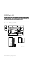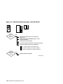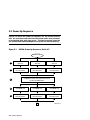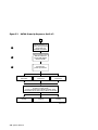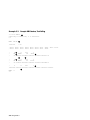
1
VAX 7000
Advanced Troubleshooting
Order Number EK–7001A–TS.001
This manual is intended for Digital customer service engineers and selfmaintenance customers. It covers system troubleshooting information.
digital equipment corporation
maynard, massachusetts
First Printing, November 1992
The information in this document is subject to change without notice and should
not be construed as a commitment by Digital Equipment Corporation.
Digital Equipment Corporation assumes no responsibility for any errors that may
appear in this document.
The software, if any, described in this document is furnished under a license and
may be used or copied only in accordance with the terms of such license. No responsibility is assumed for the use or reliability of software or equipment that is
not supplied by Digital Equipment Corporation or its affiliated companies.
Copyright © 1992 by Digital Equipment Corporation.
All Rights Reserved.
Printed in U.S.A.
The following are trademarks of Digital Equipment Corporation:
Alpha AXP
AXP
DEC
DECchip
DEC LANcontroller
DECnet
DECUS
DWMVA
OpenVMS
ULTRIX
UNIBUS
VAX
VAXBI
VAXELN
VMScluster
XMI
The AXP logo
dT
OSF/1 is a registered trademark of the Open Software Foundation, Inc.
FCC NOTICE: The equipment described in this manual generates, uses, and may
emit radio frequency energy. The equipment has been type tested and found to
comply with the limits for a Class A computing device pursuant to Subpart J of
Part 15 of FCC Rules, which are designed to provide reasonable protection against
such radio frequency interference when operated in a commercial environment.
Operation of this equipment in a residential area may cause interference, in which
case the user at his own expense may be required to take measures to correct the
interference.
Contents
Preface ..................................................................................................... vii
Chapter 1 Troubleshooting During Power-Up
1.1
1.2
1.3
1.4
1.5
1.6
1.7
1.8
1.9
Power System Overview ........................................................ 1-2
Power-Up Troubleshooting Flowchart .................................. 1-4
AC Input Box .......................................................................... 1-6
H7263 Power Regulators ....................................................... 1-8
Cabinet Control Logic Module ............................................. 1-10
Control Panel ........................................................................ 1-12
Blower ................................................................................... 1-14
XMI Plug-In Unit ................................................................. 1-16
Troubleshooting the XMI Plug-In Unit ............................... 1-18
Chapter 2 System Self-Test
2.1
2.2
2.3
2.4
2.4.1
2.4.2
2.4.3
2.4.4
2.4.5
2.5
2.5.1
2.5.2
2.5.3
System Self-Test Overview .................................................... 2-2
Power-Up Sequence ............................................................... 2-4
System Self-Test Results ..................................................... 2-10
Checking Self-Test Results: Console Display ..................... 2-12
Processor Fails Self-Test in a Uniprocessor System .... 2-14
Processor Fails ST1 in a Multiprocessor System ......... 2-16
Processor Fails ST2 or ST3 in a Multiprocessor
System ............................................................................ 2-18
Memory Fails Self-Test ................................................. 2-20
System Fails Power-Up Exerciser ................................ 2-22
Checking Self-Test Results: Status LEDs ......................... 2-24
Processor LEDs .............................................................. 2-26
Determining Failing Test Number from LEDs ............ 2-28
IOP, DWLMA, and Clock Card LEDs .......................... 2-30
iii
Chapter 3 Diagnostics
3.1
3.2
3.3
3.3.1
3.3.2
Test Command ....................................................................... 3-2
Running ROM-Based Diagnostics on XMI Devices .............. 3-4
Running Diagnostics on DUP-Based Devices ....................... 3-8
Testing an SI Device ........................................................ 3-8
Testing a DSSI Device ................................................... 3-12
Appendix A Parse Trees
A.1
Reading Parse Trees .............................................................. A-2
Appendix B Power Requirements and Guidelines
B.1
B.2
B.2.1
B.2.2
B.3
B.4
B.5
Power System Requirements ................................................. B-2
Getting Information on Power Regulator Status ................. B-3
Brief Data Packet ............................................................ B-5
Full Data Packet .............................................................. B-7
Show Power Command ........................................................ B-13
Checking the IOP Module During Power-Up ..................... B-13
Identifying an LSB Module Power Converter Failure ....... B-15
Examples
Example 2-1 Self-Test Display ................................................................. 2-12
Example 2-2 Console Display: Processor Fails in Uniprocessor System 2-14
Example 2-3 Console Display: Processor Fails ST1 in Multiprocessor
System .................................................................................. 2-16
Example 2-4 Console Display: Processor Fails ST2 or ST3 in a
Multiprocessor System ........................................................ 2-18
Example 2-5 Console Display: Memory Fails Self-Test ......................... 2-20
Example 2-6 Console Display: Sample Unexpected Exception/Interrupt ....................................................................................... 2-22
Example 2-7 Console Display: Sample Diagnostic Error Report ........... 2-23
Example 3-1 Test Commands ..................................................................... 3-2
Example 3-2 Sample RBD Session, Test Passing ..................................... 3-4
Example 3-3 Sample RBD Session, Test Failing ....................................... 3-6
Example 3-4 Testing an SI Device ............................................................. 3-8
Example 3-5 Testing a DSSI Device ........................................................ 3-12
Example A-1 Sample Machine Check, MCHK Code 06 ............................ A-2
Example B-1 Sample Output, Show Power Command ........................... B-13
iv
Figures
Figure 1-1
Figure 1-2
Figure 1-3
Figure 1-4
Figure 1-5
Figure 1-6
Figure 1-7
Figure 1-8
Figure 1-9
Figure 1-10
Figure 1-11
Figure 1-12
Figure 1-13
Figure 1-14
Figure 1-15
Figure 1-16
Figure 2-1
Figure 2-2
Figure 2-3
Figure 2-4
Figure 2-5
Figure 2-6
Figure 2-7
Figure A-1
Figure A-2
Figure A-3
Figure A-4
Figure A-5
Figure B-1
Figure B-2
Figure B-3
Figure B-4
Figure B-5
Figure B-6
Figure B-7
Figure B-8
Figure B-9
Power System ......................................................................... 1-2
Power-Up Sequence ............................................................... 1-4
AC Input Box .......................................................................... 1-6
AC Input Box Troubleshooting Steps ................................... 1-7
H7263 Power Regulator LEDs .............................................. 1-8
H7263 Power Regulator Troubleshooting Steps .................. 1-9
CCL Module LEDs ............................................................... 1-10
CCL Module Troubleshooting Steps ................................... 1-11
Control Panel ........................................................................ 1-12
Control Panel Troubleshooting Steps ................................. 1-13
Blower ................................................................................... 1-14
Blower Troubleshooting Steps ............................................. 1-15
XMI Plug-In Unit LEDs ....................................................... 1-16
XMI PIU Troubleshooting Steps - 48V LED Off ................ 1-18
XMI PIU Power Connector .................................................. 1-19
XMI PIU Troubleshooting Steps - MOD OK LED Off ....... 1-20
KA7AA Power-Up Sequence, Part 1 of 3 .............................. 2-4
KA7AA Power-Up Sequence, Part 2 of 3 .............................. 2-6
KA7AA Power-Up Sequence, Part 3 of 3 .............................. 2-8
Determining Self-Test Results ............................................ 2-10
Processor and Memory Status LEDs .................................. 2-24
Processor LEDs After Self-Test ........................................... 2-26
IOP, DWLMA, and Clock Card LEDs ................................. 2-30
KA7AA Machine Check Parse Tree ...................................... A-4
KA7AA Hard Error Interrupts ............................................ A-11
KA7AA Soft Error Interrupts .............................................. A-19
IOP Interrupts ...................................................................... A-20
DWLMA Interrupts ............................................................. A-22
Command Packet Structure .................................................. B-4
Brief Data Packet Structure .................................................. B-6
Full Data Packet Structure ................................................... B-7
Full Data Packet: Values for Characters 1–6 ....................... B-8
Full Data Packet: Values for Characters 7–34 ..................... B-9
Full Data Packet: Values for Characters 35–47 ................. B-10
Full Data Packet: Values for Characters 48–54 ................. B-11
IOP Module ........................................................................... B-14
IOP Oscillator Switch Settings ........................................... B-15
Tables
Table 1
VAX 7000 Documentation ..................................................... viii
v
Table 2
Table 1-1
Table 1-2
Table 1-3
Table 1-4
Table 2-1
Table 2-2
Table 2-3
Table 3-1
Table B-1
Table B-2
Table B-3
Table B-4
Table B-5
vi
Related Documents ................................................................... x
Power Regulator LED Summary ........................................... 1-8
Control Panel LEDs During Power-Up ............................... 1-13
XMI PIU Power Regulator LEDs ........................................ 1-17
XMI PIU Power Switches - Regulator B ............................. 1-17
System Testing ....................................................................... 2-2
Test Numbers Indicated by KA7AA LEDs ......................... 2-28
DWLMA LEDs ..................................................................... 2-31
Exercisers ............................................................................... 3-3
Power Worksheet, System Cabinet Options ......................... B-2
Power Worksheet, Expander Cabinet Options ..................... B-3
Sample Brief Packet Information ......................................... B-5
Sample Full/History Packet Information ........................... B-12
LED Status When a Power Converter Fails ....................... B-15
Preface
Intended Audience
This manual is written for Digital customer service engineers and selfmaintenance customers.
Document Structure
This manual uses a structured documentation design. Topics are organized into small sections for efficient on-line and printed reference. Each
topic begins with an abstract. You can quickly gain a comprehensive overview by reading only the abstracts. Next is an illustration or example,
which also provides quick reference. Last in the structure are descriptive
text and syntax definitions.
This manual has three chapters and two appendixes, as follows:
•
Chapter 1, Troubleshooting During Power-Up, explains what
can go wrong during power-up and how to identify the cause of the
problem.
•
Chapter 2, System Self-Test, tells how to interpret the self-test
console display and module LEDs.
•
Chapter 3, Diagnostics, describes the various diagnostics used to
test the system.
•
Appendix A contains the parse trees, and Appendix B gives power
requirements and guidelines.
vii
Conventions Used in This Document
Book titles. In text, if a book is cited without a product name, that book is
part of the hardware documentation. It is listed in Table 1 along with its
order number.
Icons. The icons shown below are used in illustrations for designating part
placement in the system described. A shaded area in the icon shows the
location of the component or part being discussed.
Front
Rear
Documentation Titles
Table 1 lists the books in the VAX 7000 documentation set. Table 2 lists
other documents that you may find useful.
Table 1
VAX 7000 Documentation
Title
Order Number
Installation Kit
EK–7000A–DK
Site Preparation Guide
EK–7000A–SP
Installation Guide
EK–700EA–IN
Hardware User Information Kit
EK–7001A–DK
Operations Manual
EK–7000A–OP
Basic Troubleshooting
EK–7000A–TS
viii
Table 1 VAX 7000 Documentation (Continued)
Title
Order Number
Service Information Kit
EK–7002A–DK
Pocket Service Guide
EK–7000A–PG
Advanced Troubleshooting
EK–7001A–TS
Platform Service Manual
EK–7000A–SV
System Service Manual
EK–7002A–SV
Reference Manuals
Console Reference Manual
EK–70C0A–TM
KA7AA CPU Technical Manual
EK–KA7AA–TM
MS7AA Memory Technical Manual
EK–MS7AA–TM
I/O System Technical Manual
EK–70I0A–TM
Platform Technical Manual
EK–7000A–TM
Upgrade Manuals
KA7AA CPU Installation Guide
EK–KA7AA–IN
MS7AA Memory Installation Guide
EK–MS7AA–IN
DWLMA XMI PIU Installation Guide
EK–DWLMA–IN
H7237 Battery PIU Installation Guide
EK–H7237–IN
BA654 Disk PIU Installation Guide
EK–BA654–IN
DWMBB VAXBI PIU Installation Guide
EK–DWMBB–IN
Removable Media Installation Guide
EK–TFRRD–IN
ix
Table 2 Related Documents
Title
Order Number
General Site Preparation
Site Environmental Preparation Guide
EK–CSEPG–MA
System I/O Options
CIXCD Interface User Guide
EK–CIXCD–UG
DEC FDDIcontroller 400 Installation/Problem
Solving
EK–DEMFA–IP
DEC LANcontroller 400 Installation Guide
EK–DEMNA–IN
DEC LANcontroller 400 Technical Manual
EK–DEMNA–TM
DSSI VAXcluster Installation and Troubleshooting Manual
EK–410AA–MG
InfoServer 150 Installation and Owner’s Guide
EK–INFSV–OM
KFMSA Module Installation and User Manual
EK–KFMSA–IM
KFMSA Module Service Guide
EK–KFMSA–SV
RF Series Integrated Storage Element User Guide
EK–RF72D–UG
TF85 Cartridge Tape Subsystem Owner’s Manual
EK–OTF85–OM
Operating System Manuals
VMS Upgrade and Installation Supplement:
VAX 7000–600 and VAX 10000–600 Series
AA–PRAHA–TE
VMS Network Control Program Manual
AA–LA50A–TE
VAXclusters and Networking
HSC Installation Manual
EK–HSCMN–IN
SC008 Star Coupler User’s Guide
EK–SC008–UG
VAX Volume Shadowing Manual
AA–PBTVA–TE
Peripherals
x
Installing and Using the VT420 Video Terminal
EK–VT420–UG
LA75 Companion Printer Installation and User
Guide
EK–LA75X–UG
Chapter 1
Troubleshooting During Power-Up
This chapter gives troubleshooting information on the power system. Sections include:
•
Power System Overview
•
Power-Up Troubleshooting Flowchart
•
AC Input Box
•
H7263 Power Regulators
•
Cabinet Control Logic Module
•
Control Panel
•
Blower
•
XMI Plug-In Unit
•
Troubleshooting the XMI Plug-In Unit
Troubleshooting During Power-Up 1-1
1.1 Power System Overview
The power system consists of the AC input box, the DC distribution box, one to three power regulators, and an optional battery
plug-in unit. Figure 1-1 shows the power system.
Figure 1-1
Rear
Power System
CCL Module
Front
AC Input Box
DC Distribution Box
Power
Regulators
BXB-0052-92
1-2 Troubleshooting During Power-Up
AC Input Box
The AC input box provides the interface to the AC utility power via a
three-phase, five-wire connector with attached power cord. The AC input
box also contains the main input circuit breaker and fuses, and a power
line monitoring port.
DC Distribution Box
The DC distribution box provides the interconnect for the AC input box
and power regulators. It also functions as the:
•
Distribution point for 48 VDC system power
•
Battery pack interface to the power regulators
•
Signal interconnect from the CCL module to the power regulators
Power Regulators
The system supports up to three power regulators operating in parallel
with either one or two units required for the load. As an option, a third
power regulator can be used as a backup unit. Each power regulator provides the following:
•
48 VDC output
•
LPS OK <A:C>L signal
•
Power system status via serial data lines
•
Non-switched 48 VDC power to the CCL module
•
Status indicators for fault isolation
•
Battery charging and monitoring circuitry
•
Battery backup converter
Optional Battery Plug-In Unit (PIU)
The battery PIU provides uninterrupted power in the event of a power failure. The battery PIU can contain up to three battery packs. Each battery
pack contains four batteries. One battery pack is required for each power
regulator.
For more information:
Platform Service Manual
Troubleshooting During Power-Up 1-3
1.2 Power-Up Troubleshooting Flowchart
Figure 1-2 shows the power-up sequence.
Power-Up Sequence
Figure 1-2
System Circuit Breaker
in On Position
Circuit Breaker
Indicators
are Red
A
No
See
Section 1.3
Control
Panel LEDs
Run: Off, Key On: On
Fault: Slow
Flash
Yes
H7263 LEDs
Green: Fast Flash
Yellow:Off
See
Section 1.6
Yes
No
See
Section 1.4
H7263 LEDs
Green: On
Yellow:Off
Yes
CCL Power
LED is ON
No
No
See
Section 1.4
Yes
No
See
Section 1.5
Blower Spins Up
Yes
Turn Keyswitch
to Enable.
A
1-4 Troubleshooting During Power-Up
No
See
Section 1.7
Yes
B
BXB-0057-92
Figure 1-2 Power-Up Sequence (Continued)
B
PIU 48V LEDS
Go On
No
See Section 1.9
Yes
CCL Module
PIU LEDs
Go On
No
See Section 1.5
Yes
PIU MOD OK
LEDs Go On
No
See Sections
1.8 and 1.9
No
See Section 1.5,
Appendix B, and
Chapter 2
Yes
LSB Modules'
Self-Test LEDs
Go On
End of Power-Up
Sequence
BXB-0058-92
Troubleshooting During Power-Up 1-5
1.3 AC Input Box
The AC input box with circuit breaker is located in the upper rear
of the cabinet. The circuit breaker has four indicators (see Figure
1-3). All four indicators should be RED when the circuit breaker is
in the On position.
Figure 1-3
AC Input Box
Rear
A - Regulator slot A
B - Regulator slot B
C - Regulator slot C
S - Sensor circuit
Breaker
Indicator
C
B
A
S
BXB-0049E-92
1-6 Troubleshooting During Power-Up
The AC input box accepts three-phase power; the three leftmost indicators
on the circuit breaker show the state of each pole (one phase per pole). If
an indicator is green, the pole is in the Off position or tripped due to an
overload. If an indicator is red, the pole is in the On position and is not
tripped. The fourth rightmost indicator reflects the mechanical position of
the circuit breaker. This indicator is red when the circuit breaker is in the
On position and green when the circuit breaker is in the Off position.
Figure 1-4 shows the troubleshooting steps for the AC input box.
Figure 1-4
AC Input Box Troubleshooting Steps
C
Rear
Circuit Breaker
Indicators
are Red
B
A
S
No
Check power regulators for an input short.
Disengage power regulator and set circuit
breaker to the ON position.
If green indicator appears again,
AC inputbox is bad.
Remove & insert power regulator in another slot.
Set circuit breaker to the ON position.
If green indicator lights indicating the new slot is bad,
replace the power regulator.
BXB-0075-92
For more information:
Platform Service Manual
Troubleshooting During Power-Up 1-7
1.4 H7263 Power Regulators
The H7263 power regulators are located in the upper right front of
the cabinet. Each power regulator has a Run LED and a Fault
LED (see Figure 1-5).
H7263 Power Regulator LEDs
Figure 1-5
Run LED
Fault LED
Front
BXB-0064r-92
Table 1-1
Power Regulator LED Summary
Run (Green)
Fault (Yellow)
Condition
Off
Off
No AC power present
Off
On
Fatal fault
Fast flash
Off
AC power present.
Keyswitch in Disable position.
On
Fast flash
Nonfatal fault
On
Slow flash
Battery discharge mode
On
Off
Normal operation
1-8 Troubleshooting During Power-Up
Figure 1-6
H7263 Power Regulator Troubleshooting Steps
H7263 LEDs
Green: Fast Flash
Yellow:Off
No
LEDs off in a single-regulator system?
Move regulator to another slot and power up.
Replace regulator.
LEDs off in a multi-regulator system?
If LEDs are off on all regulators, check AC
input voltage.
If LEDs are off on one regulator, set the AC
circuit breaker to off and then on to see if
regulator responds.
Replace regulator if both LEDs remain off.
H7263 LEDs
Green: On
Yellow:Off
No
Green LED: flash fast, yellow LED:off
Check the CCL-to-regulator cable.
Check the cable from the control panel to
the CCL module.
In single-regulator system, move regulator
to another slot and power up.
In multi-regulator system, has only one
regulator failed? Replace.
Check the regulator connectors at the DC
distribution box.
BXB-0076-92
NOTE: Replace the power regulator if the LEDs indicate a fatal fault.
Nonfatal faults include:
•
Internal heatsink temperature warning
•
Power factor correction stage failed
•
Regulator/battery failed battery test (see Appendix B)
•
48V to CCL module exceeds specified limits
Troubleshooting During Power-Up 1-9
1.5 Cabinet Control Logic Module
The cabinet control logic (CCL) module is located in the upper
front of the cabinet, behind the control panel. The CCL module
controls power sequencing and is wired to the control panel, DC
distribution box, LSB backplane, blower, PIUs, optional removable
media, and expander cabinets. The module has a power LED and
four PIU enable LEDs. You can see the CCL LEDs from the rear of
the cabinet when the rear door is open.
Figure 1-7
CCL Module LEDs
Rear
Power
LED
Rear
PIU 1
PIU 2
PIU 3
PIU 4
PIU 2
Quadrant 2
PIU 4
Quadrant 4
PIU 1
Quadrant 1
PIU 3
Quadrant 3
Front
BXB-0044B-92
During power sequencing, the CCL power LED goes on to indicate that
power is present on the module. A PIU LED goes on to indicate that a PIU
is present in the quadrant and that its power regulators are enabled. Figure 1-8 shows the troubleshooting steps for the CCL module.
1-10 Troubleshooting During Power-Up
Figure 1-8
CCL Module Troubleshooting Steps
Power LED
PIU 1
PIU 2
PIU 3
PIU 4
Rear
CCL Module
Power LED
is ON
No
Check AC input voltage.
Check the cabling from the DC distribution
box to the CCL module.
Check the power regulator.
Insert the H7263 power regulator into another slot.
If CCL power LED is still off, replace the
power regulator.
Replace the CCL module.
CCL Module
PIU LEDs
Go On
No
Check the BLOWER OK signal.
Measure the voltage at the J5 connector on
the CCL module. If the BLOWER OK L signal
is deasserted and the blower is spinning, then
replace the blower.
Check the air pressure in the cabinet.
Are the H7263 filler modules inserted properly
into empty power regulator slots?
Are the LSB filler modules inserted properly
into empty LSB slots?
Check for airflow blockage at the top and bottom of
the cabinet.
BXB-0077-92
Troubleshooting During Power-Up 1-11
1.6 Control Panel
The control panel has a keyswitch and three indicator LEDs. To
power up the system, you turn the keyswitch to Enable.
Figure 1-9
Front
Control Panel
Disable
Secure
Enable
Left Expander
Restart
Key On
Right Expander
Run
Fault
Console
BXB-0015-92
The control panel LEDs are powered by the CCL module. Table 1-2 lists
the state of each control panel LED during a normal power-up. Figure
1-10 shows troubleshooting steps for the control panel.
1-12 Troubleshooting During Power-Up
Table 1-2
Control Panel LEDs During Power-Up
Action
Key On
Run
Fault
Set circuit breaker to On
Off
Off
Off
Set keyswitch to Enable
On
Off
Slow Blink
Self-test starts
On
Off
On
Modules pass self-test
On
Off
Off
Operating system boots
On
On
Off
Figure 1-10
Control Panel Troubleshooting Steps
Key On
Disable
Secure
Enable
Restart
Run
Key On
Run
Fault
Fault
Front
Control
Panel LEDs
Run: Off, Key On: On
Fault: Slow
Flash
No
Check CCL power LED.
If CCL power LED is off, replace the CCL.
If CCL power LED is on, check cabling from
the CCL module to the control panel.
Replace the control panel.
BXB-0078-92
NOTE: The Fault LED blinks fast for 8 seconds to indicate a failure at
power-up. Then the Fault LED blinks slowly until the failure condition is cleared.
Troubleshooting During Power-Up 1-13
1.7 Blower
The blower is located in the center of the cabinet.
spins up when you turn the keyswitch to Enable.
Figure 1-11
The blower
Blower
Front
BXB-0022-92
1-14 Troubleshooting During Power-Up
Figure 1-12 shows the troubleshooting steps for the blower.
NOTE: If the blower spins up but the control panel Fault LED blinks for
more than 30 seconds, check the BLOWER OK signal cable. If the
signal cable is properly connected, then replace the CCL module.
Figure 1-12
Blower Troubleshooting Steps
Front
Blower Spins Up
No
Check that 48 VDC is present.
Check the cabling from the DC distribution box
to the 5-pin connection at the blower.
Replace the blower.
BXB-0082-92
Troubleshooting During Power-Up 1-15
1.8 XMI Plug-In Unit
The XMI plug-in unit has two power regulators with indicator
LEDs and switches. You can see the power regulators through the
PIU enclosure when the front cabinet door is open.
Figure 1-13
XMI Plug-In Unit LEDs
digital
INPUT
48
INPUT
28A
Front
VOLTAGE
VDC
CURRENT
MAX
MOD OK
OC
OT
OV
48V
INPUT
48
INPUT
5A
VOLTAGE
VDC
CURRENT
MAX
MOD OK
OC
OT
OV
48V
RESET
V-OUT
DISABLE
Regulator B
MOD OK
OC
OT
OV
48V
Regulator A
MOD OK
OC
OT
OV
48V
RESET
V-OUT
DISABLE
BXB-0074-92
1-16 Troubleshooting During Power-Up
Table 1-3
XMI PIU Power Regulator LEDs
LED
Color
State
Meaning
MOD OK
Green
On
Off
Regulator is working
Regulator is not working or
V-OUT/DISABLE switch is
set to DISABLE (down).
48V
Green
On
48V is present
OC1
Yellow
On
Overcurrent condition
OT1
Yellow
On
Overtemperature condition
OV1
Yellow
On
Overvoltage condition
1The OC, OT, and OV LEDs are latching indicators. Each LED indicates that a fault condition was or is present. The condition may have been cleared, but the LED remains lit
until it is reset.
Table 1-4
XMI PIU Power Switches - Regulator B
Switch
Function
RESET
Momentary switch resets all LEDs on both regulators.
NOTE:
V–OUT
DISABLE
If resetting does not clear the OC, OT, or OV
LED, shut off the regulators and reapply power.
This action should clear the LED.
Power output for both regulators is enabled when this
switch is in the V–OUT position (up). Power output is
shut off when this switch is in the DISABLE position
(down).
Troubleshooting During Power-Up 1-17
1.9 Troubleshooting the XMI Plug-In Unit
Figure 1-14 and Figure 1-15 show the steps to take if the power
regulator 48V LED indicates a power problem. If the MOD OK
LED indicates a problem, see Figure 1-16.
Figure 1-14
XMI PIU Troubleshooting Steps - 48V LED Off
MOD OK
OC
OT
OV
48V
MOD OK
OC
OT
OV
48V
RESET
A
V-OUT
DISABLE
Front
PIU 48V LEDs
On
B
No
Check the connector for power supply
with 48V LED off (see Figure 1-15).
Check the H7263 power regulator LEDs.
Check power at the DC distribution box.
BXB-0083-92
1-18 Troubleshooting During Power-Up
Figure 1-15 XMI PIU Power Connector
_
Front
+
_
+
digital
INPUT VOLTAGE
48 VDC
INPUT CURRENT
28A MAX
MOD OK
OC
OT
OV
48V
INPUT VOLTAGE
48 VDC
INPUT CURRENT
5A MAX
MOD OK
OC
OT
OV
48V
RESET
V-OUT
DISABLE
BXB-0085-92
Troubleshooting During Power-Up 1-19
Figure 1-16 XMI PIU Troubleshooting Steps - MOD OK LED Off
MOD OK
OC
OT
OV
48V
MOD OK
OC
OT
OV
48V
RESET
A
V-OUT
DISABLE
Front
Both
MOD OK
LEDs Off
B
Yes
Check the PIU LEDs on the CCL module (see
Section 1-5).
Check that the V-OUT/DISABLE switch is in the
V-OUT (up) position.
Check the CCL-to-PIU cabling.
Is the clock card inserted in slot 7 of the I/O card cage?
.
Check
the internal bias at power regulator B .
If low, unplug regulator A and retest the bias.
Bias normal at regulator B? Replace regulator A.
Bias still low at regulator B? Replace regulator B.
Only One
MOD OK
LED Off
Yes
Replace that power regulator.
BXB-0084-92
1-20 Troubleshooting During Power-Up
Chapter 2
System Self-Test
This chapter describes self-test. Sections include:
•
System Self-Test Overview
•
Power-Up Sequence
•
System Self-Test Results
•
Checking Self-Test Results: Console Display
— Processor Fails Self-Test in a Uniprocessor System
— Processor Fails ST1 in a Multiprocessor System
— Processor Fails ST2 or ST3 in a Multiprocessor System
— Memory Fails Self-Test
— System Fails Power-Up Exerciser
•
Checking Self-Test Results: Status LEDs
— Overview of Processor LEDs
— Determining Failing Test Number from LEDs
— IOP, DWLMA, and Clock Card LEDs
System Self-Test 2-1
2.1 System Self-Test Overview
When the system is powered up or reset, a series of tests is run.
Table 2-1 lists the tests run during system testing.
Table 2-1
System Testing
Test Level
Test
Number of Tests
1
SROM tests
11
2
Gbus ROM tests
45
3
CPU/memory tests
10
4
Multiprocessor tests
5
IOP tests
17
6
DWLMA tests
18
7
Power-up exerciser
2-2 System Self-Test
7
Not applicable
Level 1 - SROM Tests
The first phase of CPU self-test consists of 11 SROM tests. This initial
group of diagnostics is loaded from serial ROM into the CPU’s primary
cache on power-up. The diagnostics are then executed from the primary
cache; access to the backup cache is verified, and then the backup cache is
tested.
Level 2 - Gbus ROM Tests
The Gbus ROM tests, stored in FEROM, are executed during the second
phase of the CPU self-test. These tests continue CPU testing.
Level 3 - CPU/Memory Tests
These tests verify CPU logic that cannot be tested without memory. The
CPU/memory tests also test memory logic that is not tested during the
module self-test.
Level 4 - Multiprocessor Tests
Multiprocessor tests are executed by CPUs that have passed both self-test
and CPU/memory testing. These tests verify CPU-specific logic that is not
tested during previous test levels.
Level 5 - IOP Tests
The boot processor runs tests on the IOP module.
Level 6 - DWLMA Tests
The boot processor runs tests on all DWLMA I/O adapters.
Level 7 - Power-Up Exerciser
All CPUs run the power-up exerciser.
For more information:
KA7AA CPU Technical Manual
System Self-Test 2-3
2.2 Power-Up Sequence
Figure 2-1 shows the power-up sequence for the KA7AA processors. All processors execute three test phases and a boot processor
is designated after each test phase. The boot processor tests the
IOP module and DWLMA adapters and prints the self-test display.
Figure 2-1
KA7AA Power-Up Sequence, Part 1 of 3
Power-Up
1
CPU 1
Self-Test
CPU 2
Self-Test
CPU n
Self-Test
2
Determine
Boot Processor
Determine
Boot Processor
Determine
Boot Processor
Boot processor prints self-test results,
configures memory, and signals other CPUs
to start CPU/MEM tests.
3
4
CPU 1
CPU/MEM Test
CPU 2
CPU/MEM Test
CPU n
CPU/MEM Test
5
Determine
Boot Processor
Determine
Boot Processor
Determine
Boot Processor
A
2-4 System Self-Test
BXB-0018-92
1
All CPUs and memories execute their on-board self-test at the beginning of the power-up sequence. On line ST1 of the self-test display, a
plus sign (+) is shown for every module that passes self-test.
2
The boot processor is determined. On the first BPD line, the letter B
corresponds to the processor selected as boot processor. Because the
processors have not yet completed their power-up tests, the designated
processor may later be disqualified from being boot processor. For this
reason, line BPD appears three times in the self-test display.
3
The boot processor prints the results of self-test, lines NODE #, TYP,
ST1, and BPD on the self-test display. The boot processor then signals all CPUs to start running the CPU/MEM tests.
4
All CPUs execute the CPU/MEM tests using the memories. On line
ST2 of the self-test display, a plus sign (+) is shown for every module
that passes the CPU/MEM test. If all CPUs pass the CPU/MEM
tests, then the original boot processor selection is still valid.
5
The boot processor is again determined, for the second time. Results
are printed on the BPD line.
System Self-Test 2-5
Figure 2-2
KA7AA Power-Up Sequence, Part 2 of 3
A
Boot processor prints
CPU/MEM
test results
6
7
CPU 1
MP Tests
CPU 2
MP Tests
CPU n
MP Tests
8
Determine
Boot Processor
Determine
Boot Processor
Determine
Boot Processor
9
Boot processor copies
console to memory and
begins executing in
multiprocessor mode
Boot processor prints MP test results
and then runs IOP tests
B
BXB-0019-92
2-6 System Self-Test
6
The boot processor prints line ST2 and the second BPD of the self-test
display. If no processor is selected as the boot processor, an error message is displayed and the console hangs (see Section 2.4.1).
7
All passing CPUs execute the multiprocessor tests. On line ST3 of the
self-test display, a plus sign (+) is shown for every module that passes
the multiprocessor tests. If all CPUs pass the multiprocessor tests,
then the original boot processor selection is still valid.
8
The boot processor is again determined, for the third time. Results are
printed on the BPD line.
9
The boot processor copies the console to memory and begins executing
in multiprocessor mode. Next, the boot processor prints the results of
the multiprocessor tests on the ST3 line and then executes the IOP
tests.
System Self-Test 2-7
Figure 2-3
KA7AA Power-Up Sequence, Part 3 of 3
B
10
DWLMA adapters are
tested. Boot processor
reports IOP and
DWLMA test results.
11
Boot processor probes
XMI I/O buses and
reports XMI adapter
self-test results.
12
All CPUs run
power-up exerciser.
CPU 1
Exercisers
CPU 2
Exercisers
CPU n
Exercisers
Boot processor boots operating system
or halts in console mode.
If boot processor boots operating system, starts
all attached CPUs after boot processor has booted.
CPU 1
running
CPU 2
running
CPU n
running
BXB-0020-92
2-8 System Self-Test
10
DWLMA adapter test results are indicated on the lines labeled C0
XMI to C3 XMI on the self-test display. A plus sign (+) at the extreme
right means that the adapter passed; a minus sign (−) means that the
adapter failed. IOP test results are indicated on line ST3.
11
If the DWLMA adapter passes its self-test, then the boot processor reports the self-test results for each XMI adapter.
12
Testing continues. All CPUs execute the power-up exercisers. Specific
exercisers test the following:
•
Cache/memory
•
Floating point
•
Network
•
Disk (internal loopback only)
System Self-Test 2-9
2.3 System Self-Test Results
The results of self-test can be determined in three ways.
Figure 2-4
Determining Self-Test Results
Key On
Disable
Secure
Enable
Run
Restart
Key On
Fault
Run
Fault
Front
Front
Rear
Self-Test LEDs
F
E
D
C
B
A
9
8
A
o
.
o
.
+
.
7
M
+
.
+
.
+
.
6
.
.
.
.
.
.
.
5
.
.
.
.
.
.
.
4
.
.
.
.
.
.
.
3
.
.
.
.
.
.
.
2
.
.
.
.
.
.
.
1
P
+
E
+
B
+
B
.
+
.
.
.
.
.
.
.
.
.
.
.
.
.
.
.
.
.
.
.
.
.
.
.
+
.
.
.
.
.
.
.
.
.
.
.
.
.
.
.
.
.
.
.
.
.
.
.
.
.
.
.
.
.
. A0 .
. 128 .
.
.
.
.
.
.
.
.
.
.
Firmware Rev = V1.0-1625
SROM Rev = V1.0-0
0
P
+
B
E
E
NODE #
TYP
ST1
BPD
ST2
BPD
ST3
BPD
C0 XMI C1 XMI +
C2
C3
.
.
ILV
128Mb
SYS SN = GAO1234567
BXB-0086-92
2-10 System Self-Test
There are three ways to check the results of self-test:
•
Control panel Fault LED. This LED remains lit if a processor, a
memory, an IOP module, or an XMI adapter fails self-test.
•
Module LEDs. The LEDs on the LSB modules display the results of
self-test, as described in Section 2.5.
•
Console terminal. A summary report of self-test appears on the console terminal. This summary report is described in Section 2.4.
System Self-Test 2-11
2.4 Checking Self-Test Results: Console Display
The console display gives the results of module self-tests and additional testing.
Example 2-1
Self-Test Display
F
A
E
.
+
.
.
D
.
.
.
.
C
.
.
.
.
B
.
.
.
.
.
.
.
.
9
.
.
.
.
8
A
o
.
o
.
+
.
7
M
+
.
+
.
+
.
6
.
.
.
.
.
.
.
5
.
.
.
.
.
.
.
4
.
.
.
.
.
.
.
3
.
.
.
.
.
.
.
2
.
.
.
.
.
.
.
1
P
+
E
+
E
+
E
.
+
.
.
.
.
.
.
.
.
.
.
.
.
.
.
.
.
.
.
.
.
.
.
.
.
.
.
.
.
.
. A0 .
. 128 .
.
.
.
.
.
.
.
.
.
.
0
P
+
B
+
B
+
B
NODE #
TYP
ST1
BPD
ST2
BPD
ST3
BPD
C0 XMI C1 XMI +
C2
C3
.
.
1
2
3
4
5
6
7
8
9
10
ILV
128Mb
Firmware Rev = V1.0-1625 SROM Rev = V1.0-0 SYS SN = GAO1234567 11
P00>>>
1
The first line lists the node numbers on the LSB and XMI I/O buses.
2
This line indicates the type of module at each LSB node. Processors
are type P, memories are type M, and the IOP module is type A. In
this example processors are at nodes 0 and 1, a memory is at node 7,
and the IOP module is at node 8.
3
This line shows the results of on-board self-test. Possible values for
processors are pass (+) or fail (−). For memories, the pass (+) value
indicates successful completion of self-test. (Self-test failure indications are shown in Example 2-2 and Example 2-3.) The "o" at node 8
(IOP module) indicates no on-board self-test.
2-12 System Self-Test
4
The BPD line indicates boot processor designation. When the system
completes on-board self-test, the processor with the lowest LSB ID
number that passes self-test and is eligible is selected as boot processor. This process occurs again after ST2 and ST3 when the boot processor designation is reported on the second and third BPD lines.
5
During the second round of tests (ST2), all processors run CPU/MEM
tests. On line ST2, results are reported for each processor and memory; a plus sign (+) indicates that ST2 testing passed and a minus sign
(−) that ST2 testing failed. The boot processor is again reported on the
BPD line.
6
During the third round of tests (ST3), all processors run multiprocessor
tests. Results are reported on line ST3, and the boot processor designation is again reported on the third and final BPD line.
7
A minus sign (−) at the right of the C0 XMI line means that the
DWLMA adapter on I/O channel 0 failed self-test. Self-test results for
adapters on this I/O channel will not be reported.
8
A plus sign (+) at the right of the C1 XMI line indicates that the
DWLMA adapter on I/O channel 1 passed self-test. However, the
adapter at XMI node 3 failed its own self-test. I/O channels C2 ( 9 )
and C3 ( 10 ) are not used in this configuration.
11
The last line of the self-test display shows the console firmware and
SROM version numbers and the system serial number.
For more information:
Basic Troubleshooting
System Self-Test 2-13
2.4.1 Processor Fails Self-Test in a Uniprocessor System
When the processor in a uniprocessor system fails self-test, the operator is prompted for the slot number of the processor. Where
the error message appears in the console display indicates the
round of tests the processor failed: ST1, ST2, or ST3. See Example
2-2.
Example 2-2
Console Display: Processor Fails in Uniprocessor
System
>>> init
CPU00: Test Failure - Select primary CPU
F
E
7 6 5 4 3 2
M . . . . .
+ . . . . .
. . . . . .
CPU00: Test Failure - Select primary CPU
o + . . . . .
. . . . . . .
CPU00: Test Failure - Select primary CPU
+ + . . . . .
. . . . . . .
.
.
.
.
D
.
.
.
.
C
.
.
.
.
B
.
.
.
.
A
+
.
.
.
9
.
.
.
.
8
A
o
.
+
.
.
.
1
1
.
.
.
0
P
B
NODE #
TYP
ST1
BPD
.
.
B
ST2
BPD
.
.
B
ST3
BPD
1
1
.
.
.
.
+
.
.
.
.
.
.
.
.
.
.
.
.
.
.
.
+
.
.
.
.
.
.
.
. A0
.128
.
.
.
.
.
.
.
.
.
.
.
.
C0 XMI +
C1
C2
C3
.
.
ILV
128Mb
Firmware Rev = V1.0-1625 SROM Rev = V1.0-0 SYS SN = GAO1234567
>>>
2-14 System Self-Test
Example 2-2 shows a processor failure in a uniprocessor system.
The error message, CPU00: Test Failure - Select primary CPU,
prompts you to enter the node ID of the failing processor. Note that the
CPU node ID appears in the error message (CPU00). Type 0 to obtain the
full console display. If you do not type the node ID when prompted, the
processor continues to hang.
NOTE: The user input in response to the error message is not echoed at the
console terminal.
Possible Solutions
•
•
Move the processor to another slot and retry self-test.
Replace the failing processor with a new processor (see the System
Service Manual).
System Self-Test 2-15
2.4.2 Processor Fails ST1 in a Multiprocessor System
When a processor in a multiprocessor system fails self-test at ST1,
no failure information is reported to the console display. Only
passing processors show in the console display.
Example 2-3
Console Display: Processor Fails ST1 in
Multiprocessor System
F
E
D
C
B
A
9
8
A
o
.
o
.
+
.
7
M
+
.
+
.
+
.
6
M
+
.
+
.
+
.
5
.
.
.
.
.
.
.
4
.
.
.
.
.
.
.
3
.
.
.
.
.
.
.
2
.
.
.
.
.
.
.
1
P
+
B
+
B
+
B
.
.
.
.
.
.
.
.
.
.
.
.
.
.
.
.
+
.
.
.
.
.
.
.
+
.
.
.
.
.
.
.
+
.
.
.
.
.
.
.
.
.
.
.
.
.
.
.
+
.
.
.
.
.
.
.
. A1 A0
.128128
.
.
.
.
.
.
.
.
.
.
0 1 NODE #
. TYP
. ST1
. BPD
. ST2
. BPD
. ST3
. BPD
C0 XMI +
C1
C2
C3
.
.
ILV
256Mb
Firmware Rev = V1.0-1625 SROM Rev = V1.0-0 SYS SN = GAO1234567
>>>
2-16 System Self-Test
When a processor fails ST1 testing in a multiprocessor system, no information is reported, and the failing processor is logically disconnected from the
backplane to prevent faulty system operation. Dots are displayed, as
though no processor were physically present.
In this example the processor in slot 0 fails ST1 (see 1 ). If the processor
in slot 1 failed ST1, then the column for slot 1 would report no information.
To confirm a processor failure at ST1, open the LSB card cage and check
the module positions against the self-test display. If you find a processor
occupying a slot that is not reporting to the self-test display, check the
CPU LED lights for test failure information.
Possible Solutions
•
Check module seating in the LSB card cage. Remove the failing module and re-insert it; check that the module case is in the tracks and
latched securely.
•
Place a passing processor in the failing slot; if the passing processor
fails, you may have a bad LSB slot. Next, take the failing module and
try it in a slot where a module has passed self-test. If the failing processor now passes self-test, avoid using the slot in which both processors failed testing.
•
Replace the failing processor with a new processor (see the System
Service Manual).
System Self-Test 2-17
2.4.3 Processor Fails ST2 or ST3 in a Multiprocessor System
Example 2-4 shows a multiprocessor system with ST2 and ST3 failures. Since ST2 is a CPU/memory test, the example shows a memory failure to illustrate the CPU/memory interaction.
Example 2-4
Console Display: Processor Fails ST2 or ST3 in a
Multiprocessor System
F
A
E
.
.
.
.
D
.
.
.
.
C
.
.
.
.
B
.
.
.
.
+
.
.
.
9
.
.
.
.
8
A
o
.
o
.
+
.
7
M
+
.
+
.
+
.
6
M
+
.
+
.
+
.
5
.
.
.
.
.
.
.
4
.
.
.
.
.
.
.
3
.
.
.
.
.
.
.
2
P
+
E
+
E
+
B
1
P
+
E
+
B
E
+
.
.
.
.
.
.
.
+
.
.
.
.
.
.
.
.
.
.
.
.
.
.
.
+
.
.
.
.
.
.
.
0
P
+
B
E
E
NODE #
TYP
ST1
BPD
ST2
BPD
ST3
BPD
1
2
3
C0 XMI +
C1
C2
C3
. A1 A0 . . . . . . ILV
.128128 . . . . . . 256Mb
Firmware Rev = V1.0-1625 SROM Rev = V1.0-0 SYS SN = GAO1234567
P02>>>
2-18 System Self-Test
Processors can fail ST1, ST2, or ST3 testing. When a processor fails ST1
or ST2, subsequent ST lines will also indicate failure.
1
The ST1 line shows that each of the three CPUs passed the first round
of testing. The two memories successfully completed ST1 also.
2
ST2 is the CPU/memory test. The ST2 line shows the CPU in slot 0
failing. Consequently, the failing CPU is no longer designated as the
boot processor. The CPUs in slots 1 and 2 conduct the CPU/memory
tests. The memories in slots 6 and 7 pass ST2 testing.
3
Only the CPUs in slots 1 and 2 undergo ST3 testing; the processor in
slot 0 is not tested because of its previous failure during ST2 testing.
In the example, the CPU in slot 1 fails the third round of testing.
Possible Solutions
•
Reseat processors in slots 0 and 1 and repeat testing.
•
Place passing CPU in failing slot and if the passing CPU fails, you may
have a bad LSB slot. Next, take the failing CPU and try it in a slot
where a module has passed self-test. If the failing CPU now passes
self-test, avoid using the slot in which both processors failed testing.
•
Replace the failing processor with a new processor (see the System
Service Manual).
System Self-Test 2-19
2.4.4 Memory Fails Self-Test
A minus sign (−) at ST1 indicates that the on-board self-test was
unable to complete. A minus sign at ST2 or ST3 following a plus
sign (+) at ST1 indicates errors in the CPU/memory tests.
Example 2-5
Console Display: Memory Fails Self-Test
F
E
D
C
B
A
9
8
A
o
.
o
.
+
.
7 6
M M
1
- +
. .
2
- +
. .
- 3+
. .
5
.
.
.
.
.
.
.
4
.
.
.
.
.
.
.
3
.
.
.
.
.
.
.
2
.
.
.
.
.
.
.
1
P
+
E
+
E
+
E
.
.
.
.
.
.
.
.
.
.
.
.
.
.
.
.
+
.
.
.
.
.
.
.
+
.
.
.
.
.
.
.
.
.
.
.
.
.
.
.
.
.
.
.
+
.
.
.
.
.
.
.
.
. A0 . . . . . . ILV
. 128 . . . . . . 128Mb
.
+
.
.
.
0
P
+
B
+
B
+
B
NODE #
TYP
ST1
BPD
ST2
BPD
ST3
BPD
C0 XMI +
C1
C2
C3
4
Firmware Rev = V1.0-1625 SROM Rev = V1.0-0 SYS SN = GAO1234567
P00>>>
2-20 System Self-Test
At power-up or reset, each memory module executes a self-test designed to
test and initialize its RAMs. The self-test performs a quick scan of the
DRAM array and records sections of the array that contain defective locations. These sections will eventually be mapped out by the console and
will no longer be included in the console bitmap. The operating system
uses this bitmap to determine which memory to use and not to use.
The memory self-test does not provide a pass/fail status. The module LED
indicates only that self-test completed. The length of testing depends on
the size of the memory array.
In Example 2-5:
1
The failure reported at ST1 indicates that the memory module at node
7 is unable to complete its on-board self-test. Consequently, the selftest LED on the memory module remains unlit.
2
The CPU/memory tests are run on the passing memory at node 6. The
failed memory at node 7 is not used during this testing. The ST2 line
indicates that both processors and one memory module passed the
CPU/memory test.
3
The failing memory is not used during ST3 testing. The minus sign
appears only to identify the memory as a failing FRU.
4
The memory at node 6 is configured in the system. The memory at
node 7 is not configured because of its failure during ST1.
System Self-Test 2-21
2.4.5 System Fails Power-Up Exerciser
When the system fails the power-up exerciser, an error message is
displayed at the console terminal. The error message is either an
unexpected exception/interrupt (Example 2-6) or a diagnostic error report (Example 2-7), depending on the type of error found.
See Appendix A for parse trees.
Example 2-6
Console Display: Sample Unexpected
Exception/Interrupt
CPU2: unexpected exception/interrupt, vector 60 (18) 1
process entry_02, pcb = 000dad60, pc: 0007feed psl: 00000004
Interrupt/Exception: hard error notification
LMERR: 00000180 LMODE: 000102a0 LBER: 0004121f LLOCK: 00004430 2
LDEV: 00008002 LCNR: 00000001 LBESR0:0000000c LBESR1:0000000c
LBESR2:0000000c LBESR3:0000000c LBECR0:1f555555 LBECR1:00001000
3
BIU_CTL: afe09ff8 DIAG_CTL: 00000001 BC_TAG: 00003800 BIU_STAT: f01e10a1
BIU_ADDR:eaaaaaae FILL_SYN: 00000000 FILL_ADDR: 000002a8
gprs:
0: 0000001F
1: 0008E478
2: 0008E478
3: 0008E478
4: 00000000
5: 00000000
6: 00000002
7: 00000004
8: 00083B10
9: 00088610
10: 00000000
11: 00000000
12: 000DBE8C
13: 000DBE74
14: 0007FEED
ksp: 000DBE74 esp: 00000000 ssp: 00000000 usp: 00000000
1
A hard error (vector 60) was detected.
2
These are the relevant error registers in the CPU bus interface gate array.
3
These are the internal processor error registers (IPRs).
2-22 System Self-Test
Example 2-7
Console Display: Sample Diagnostic Error Report
*** Hard Error - Error #23 on FRU: MS7AA1 1
Memory compare error
ID Program
Device
Pass Hard/Soft Test
Time
6
7 ---- 8-------- 9
-------- 2--------3 --------------- 4--------5 --------8e
mem_ex
mem
6
1
0
1 03:07:01
Expected value:
Received value:
Failing addr:
ffffff71 10
fffffe71
010003d0
***End of Error***
1
A hard error, error #23, is reported on FRU MS7AA1, a memory module. The three types of errors reported are hard, soft, and fatal. The
error number, in this case error #23, corresponds to the location of the
actual error report call within the source code for the failing diagnostic.
2
The process identification number (ID) is 8e. This is the process ID of
the failing diagnostic.
3
The program running when the error occurred is mem_ex, the memory
exerciser.
4
The device being tested at the time of the error. The device name in
this field may or may not match the device mnemonic displayed in the
FRU field ( 1 ).
5
The current pass count, 6, is the number of passes executed when the
error was detected.
6
The current hard error count is 1. The hard and soft error counts are
the number of errors detected and reported by the failing diagnostic
since the testing started.
7
The current soft error count is 0.
8
In this example, the failing test number is 1.
9
The time stamp shows when the error occurred.
10
The expected and received values at failing address 010003d0 are reported.
System Self-Test 2-23
2.5 Checking Self-Test Results: Status LEDs
You can check self-test results by looking at the status LEDs on
the modules. The processor diagnostic LEDs are described in Section 2.5.1 and Section 2.5.2. The LEDs on the IOP module, DWLMA
adapter, and clock card are described in Section 2.5.3.
Figure 2-5
Processor and Memory Status LEDs
Module
Enclosure
Front
SGO123456789
Processor
LED Window
Power LED
E2043-AA
REV 0.3
Rear
Self-Test
Completed
LED
Processor
Memory
BXB-0090C-92
2-24 System Self-Test
Processor Status LEDs
The large green LED at the bottom of the processor lights when the module passes self-test. You can see this LED through the peephole on the
module enclosure.
To view the diagnostic LEDs on a failing processor:
1.
Open the front door of the cabinet.
2.
Release the plate covering the modules by loosening the two top
screws.
3.
Remove the opaque plastic window covering the diagnostic LEDs on
the processor by pulling it out with your fingers.
Section 2.5.1 describes the diagnostic LEDs on the processor module.
Memory Status LEDs
A memory module has two green LEDs: a self-test completed LED and a
power LED. The self-test completed LED lights when the module completes self-test. This LED is visible through the peephole on the module
enclosure. The power LED lights to indicate that power is present on the
module.
System Self-Test 2-25
2.5.1 Processor LEDs
The processor LEDs display the results of self-test. You must remove the plate covering the card cage and the plastic window on
the processor module to view the diagnostic LEDs.
Figure 2-6
Processor LEDs After Self-Test
Self-Test Passed
Self-Test Failed
MSB
Front
Off
Off
*
LSB
On
On
On
Boot
On
Secondary
Off
Off
* Failing
Test Number
BXB-0090D-92
2-26 System Self-Test
When self-test passes, the processor’s LEDs are set as shown in Figure 2-6.
The two LEDs closest to the self-test LED are on if the KA7AA is the boot
processor; the LED closest to the self-test LED is on if the KA7AA is a secondary processor.
If self-test fails for the processor or the memory module fails, the top seven
processor LEDs contain an error code that corresponds to the number of
the failing test. The test number is represented in binary-coded decimal,
with the most significant bit at the top. A bit is ONE if the light is ON.
For example, assume a processor fails its self-test (large green LED is
OFF) and shows the following pattern in the top seven LEDs:
TOP
(MSB) off
on
on
0 = 3
1
1
off
off
on
(LSB) off
0
0
1 = 2
0
BOTTOM
The failing test number decodes to 011 0010 (binary-coded decimal 32).
Section 2.5.2 gives more detail on the failing tests indicated by the processor LEDs.
System Self-Test 2-27
2.5.2 Determining Failing Test Number from LEDs
When self-test fails, the top seven green LEDs on the processor indicate the test number. A failing test number is in binary-coded
decimal.
Table 2-2
Test Numbers Indicated by KA7AA LEDs
Test Number
Type of Test
Failing Device
Self-Test Line
1–11
SROM tests
KA7AA
ST1
12–59
GROM tests
KA7AA
ST1
60–69
CPU/memory tests
KA7AA or
MS7AA
ST2
70–76
Multiprocessor tests
KA7AA
ST3
2-28 System Self-Test
You can see the results of self-test from the LEDs on the processor.
KA7AA Self-Test LED Off
If the processor’s large green LED is off and the top seven small LEDs
show an error code in the range of 1 to 59, then the processor’s self-test
failed and the processor board is bad.
After the on-board self-test, each processor that passes self-test runs the
CPU/memory tests. The LEDs display error codes for failing CPU/memory
tests with numbers ranging from 60 to 69. The self-test LED on the failing
processor or the failing memory module is off.
Next, processors that pass both the on-board self-test and CPU/memory
testing run multiprocessor tests. For failing multiprocessor tests, the
LEDs display numbers ranging from 70 to 76. The self-test LED on the
processor is off.
KA7AA Self-Test LED On, IOP LED Off
The IOP module has failed testing if its LED is off. The self-test LED on
the KA7AA will be on.
System Self-Test 2-29
2.5.3 IOP, DWLMA, and Clock Card LEDs
Figure 2-7 shows the LEDs on the IOP module, the DWLMA
adapter, and the clock card.
Figure 2-7
IOP, DWLMA, and Clock Card LEDs
Yellow
Self-Test
LED
Green
Debug
Green
LED
Self-Test
LED
Green
Power-On
LED
Red Fatal
Error LED
Yellow
Power
LED
Red Error
Summary
LED
IOP Module
DWLMA Adapter
Clock Card
BXB-0361-92
2-30 System Self-Test
IOP Module LED
To view the IOP self-test LED, open the rear door of the cabinet and release the plate covering the card cage by loosening the two top screws. The
green LED is on to indicate that the IOP passed self-test.
DWLMA Adapter LEDs
Table 2-3 lists the DWLMA LEDs and their self-test passed status.
NOTE: If the DWLMA adapter fails self-test, check the clock card at node 7
in the XMI card cage. If the clock card fails testing (power LED is
off), the DWLMA adapter will also fail.
Table 2-3
DWLMA LEDs
LED
Color
Self-Test Passes
STP
(Self-test passed)
Yellow
On
DBGDIS
(Debug disabled)
Green
On
POK
(Power OK)
Green
On
FTLERR
(Fatal error)
Red
Off
ES
(Error Summary)
Red
Off
Clock Card
The clock card, XMI node 7, has a yellow LED that lights to indicate that
power is enabled in the XMI card cage. The POWER ENABLE H signal is
looped through the clock card so that the XMI power system cannot be enbled unless the clock card is properly installed.
System Self-Test 2-31
Chapter 3
Diagnostics
This chapter discusses how to test processors, memory, and I/O. Sections
include:
•
Test Command
•
Running ROM-Based Diagnostics on XMI Devices
•
Running Diagnostics on DUP-Based Devices
— Testing an SI Device
— Testing a DSSI Device
Diagnostics 3-1
3.1 Test Command
The test command allows you to test the entire system, an I/O subsystem, a single module, a group of devices, or a single device.
Example 3-1
Test Commands
>>> test
# Tests the entire system.
# Default run time is 10
# minutes.
>>> t xmi0 -t 60
#
#
#
#
>>> t xmi1 -omit "demna*"
# Tests all devices
# associated with XMI1 except
# for Ethernet devices.
Tests all devices
associated with the XMI0
I/O subsystem. Test
run time is 60 seconds.
>>> t -nowrite "dub*" -write -t 120
#
#
#
#
#
Do write/read/compare
testing on all disks not
associated with controller
b. Test run time is 120
seconds.
>>> t demna*
# Tests all DEMNA adapters.
>>> t du*.0.4.0
#
#
#
#
>>> t -q
# Status messages will not be
# displayed during system
# test.
3-2 Diagnostics
Tests all MSCP disks
associated with the
adapter in slot 4 of
XMI0.
You enter the command test to test the entire system using exercisers. No
module self-tests are executed when the test command is issued without a
mnemonic.
When you specify a subsystem mnemonic or a device mnemonic with test
such as test xmi0 or test ka7aa1, self-tests are executed on the associated modules first and then the appropriate exercisers are run. Table 3-1
lists the exercisers associated with each module.
The same set of tests that run at power-up will run if you enter a test iop0
or a test dwlman command.
Table 3-1
Exercisers
Module
Module Self-Test Run?
Exerciser
KA7AA
Yes
Floating Point,
Multiprocessor,
Memory
MS7AA
No
Memory
CIXCD
Yes
Disk
DEMFA
Yes
Network
DEMNA
Yes
Network
KDM70
Yes
Disk
KFMSA
Yes
Disk
Disk Device
No
Disk
NOTE: Testing tape devices is not supported by the test command. Run
DUP-based tests to test an MSCP-based tape device. See Section
3.3.
Diagnostics 3-3
3.2 Running ROM-Based Diagnostics on XMI
Devices
Some XMI devices can be tested from the console terminal with
their on-board ROM-based diagnostics (RBDs). The set host command is used to connect to the XMI device. Example 3-2 shows a
passing RBD test display, and Example 3-3 shows a test failure display.
Example 3-2
Sample RBD Session, Test Passing
>>> sh config
1
Name
Type
Rev
Mnemonic
LSB
0+
7+
8+
KA7AA
MS7AA
IOP
(8002)
(4000)
(2000)
0000
0000
0001
ka7aa0
ms7aa0
iop0
C0 XMI
8+
C+
E+
DWLMA
KDM70
DEMNA
(102A)
(0C22)
(0C03)
0104
1E11
0802
xmi0
dwlma0
kdm700
demna0
2
>>> set h demna0 3
Connecting to remote node, ^Y to disconnect.
t/r 4
RBDE> ST0/TR
5
;Selftest
3.00
; T0001 T0002 T0003 T0004 T0005 T0006 T0007 T0008 T0009 T0010
; T0011 T0012 T0013 T0014 T0015 T0016 T0017 T0018
E
0C03
1
;
P 6
;00000000 00000000 00000000 00000000 00000000 00000000 00000000
RBDE> ^Y
>>> 8
7
3-4 Diagnostics
1
The show configuration command shows that this system includes a
DEMNA at XMI0 node E.
2
The assigned mnemonic for the DEMNA is demna0.
3
The set host demna0 command is typed at the console prompt. A
connection is established to the DEMNA adapter. A message confirms
that the connection has been made.
4
After the console message no prompt is displayed. Typing t/r invokes
the RBD monitor on the adapter being tested and returns the RBD
monitor prompt. Note that the E in the RBD prompt refers to the XMI
node.
5
The RBD is started with trace set.
6
This field indicates whether the RBD passed or failed; P for passed, F
for failed.
7
Enter Ctrl/Y to exit from the RBD monitor.
8
The console prompt returns.
For more information:
VAX 6000 Model 600 Service Manual
Diagnostics 3-5
Example 3-3
Sample RBD Session, Test Failing
>>> set h demna0 1
Connecting to remote node, ^Y to disconnect.
t/r
RBDE> ST0/TR
2
;Selftest
3.00
; T0001
; T0011
;
;
;
;
;
;
T0002
T0012
T0003
T0013
T0004
T0014
T0005
T0015
T0006
T0016
T0007
T0017
T0008
T0018
T0009
E
0C03
1
F 3
HE 4 XNAGA
XX
T0018 5
03 00000000 0000A000 00000000 20150004 20051D97 08
6
7
F 8
E
0C03
1
HE
XNAGA
XX
T0018
05 00020000 80020000 00000000 20150204 200524A4 01
;
F
E
0C03
1 9
;00000000 00000002 00000000 00000000 00000000 00000000 00000000
10
RBDE> ^Y
>>>
3-6 Diagnostics
T0010
1
The set host demna0 command is typed to establish the connection to
the DEMNA adapter. A message confirms that the connection has
been made.
2
The RBD is started with trace set.
3
F indicates the first failure during T0018, or test 18.
4
The class of error is displayed here. HE indicates that the error was a
hard error. SE means that the error was a soft error, and FE indicates
a fatal error.
5
This field lists the number of the test that failed; test 18 failed here.
6
The expected data is shown here. 00000000 is the data test 18 expected.
7
The received data is shown here. 0000A000 is the data test 18 received.
8
F indicates the second failure during test 18.
9
This is the summary line, and a repeat of the failure summary. It lists
the pass/fail code (P or F), the node number and device type number of
the device executing the RBD, and the number of passes of the RBD.
10
This is the number of hard errors detected.
For more information:
VAX 6000 Model 600 Service Manual
Diagnostics 3-7
3.3 Running Diagnostics on DUP-Based Devices
To run diagnostics on a DUP-based device, enter the set host command to invoke the DUP server on the selected node. You can test
devices associated with the KDM70 (SI) adapter or the KFMSA
(DSSI) adapter.
3.3.1 Testing an SI Device
Example 3-4 is a sample test session of an SI device. The device
tested is a disk associated with the KDM70 adapter.
Example 3-4
Testing an SI Device
>>> show device 1
polling for units on kdm700, slot 11, xmi0...
duc1.0.0.11.2
DUC1
RA70
duc2.0.0.11.2
DUC2
RA70
duc3.0.0.11.2
DUC3
RA70
duc213.0.0.11.2
DUC213
RA82
>>> set host -dup duc1.0.0.11.2 2
dup: starting DIRECT on kdm70_c.0.0.11.2 ()
DIRECT
1
D Directory Utility
ILEXER
1
D InLine Exerciser
Task? ilexer 3
dup: starting ILEXER on kdm70_c.0.0.11.2 ()
3-8 Diagnostics
1
Type show device to obtain a list of disks and device mnemonics.
2
Enter set host -dup to connect to the disk you want to test. In the
example, the disk with the mnemonic duc1.0.0.11.2 is selected. The
DUP program prompts you to select Directory Utility or InLine Exerciser.
3
Type ilexer to start the inline exerciser.
For more information:
KDM70 Controller User Guide
KDM70 Controller Service Manual
Diagnostics 3-9
Example 3-4
Testing an SI Device (Continued)
***
*** ILEXER (InLine Exerciser) V 001
***
*** 17-NOV-1992 03:10:28 ***
Enable Bad Block Replacement (Y/N) [N] ?
4
Available Disk Drives: D0001 D0002 D0003 D0213
Available Tape Drives: NONE
Select next drive to test (Tnnnn/Dnnnn) [] ? d0003
Write enable drive (Y/N) [N] ?
5
*** Available tests are:
1.
2.
3.
4.
Select
Select
Select
Select
Select
Select
Select
Select
Report
Random I/O
Seek Intensive I/O
Data Intensive I/O
Oscillatory Seek
test number (1:4) [1] ?
start block number (0:547040) [0] ?
end block number (0:547040) [547040] ?
data pattern number 0=ALL (0:15) [0] ?
another drive (Y/N) [] ? n
execution time limit, 0=Infinite, minutes (0:65535) [0] ? 1
report interval, minutes (0:65535) [1] ?
hard error limit (0:32) [0] ?
soft errors (Y/N) [N] ?
Execution Performance Summary at 17-NOV-1992 03:12:36 6
D0003
7
193531233
8
1998
9
4508
10
0
11
0
12
0
0
13
14
Execution Performance Summary at 17-NOV-1858 00:02:37
D0003 *
193531233
***
*** ILEXER is exiting.
***
3-10 Diagnostics
2003
4513
0
0
0
0
4
You are prompted to answer a series of questions before testing can begin.
5
Indicate the disk drive to be tested.
6
The execution performance summary line includes the following entries:
7
Unit number
8
Unit serial number
9
Number of requests issued
10
Kbytes read
11
Kbytes written
12
Hard error count
13
Soft error count
14
ECC error count
Diagnostics 3-11
3.3.2 Testing a DSSI Device
Example 3-5 is a sample test session of a DSSI device. The device
tested is a disk associated with the KFMSA adapter.
Example 3-5
Testing a DSSI Device
>>> set host -dup duc1.1.0.13.3 1
dup: starting DIRECT on kfmsa_c.1.0.13.3 (R2UJBC)
2
Copyright (C) 1990 Digital Equipment Corporation
PRFMON V1.0 D 20-FEB-1991 09:49:00 3
DKCOPY V1.0 D 20-FEB-1991 09:49:00
DRVEXR V2.0 D 20-FEB-1991 09:49:00
DRVTST V2.0 D 20-FEB-1991 09:49:00
HISTRY V1.1 D 20-FEB-1991 09:49:00
DIRECT V1.0 D 20-FEB-1991 09:49:00
ERASE V2.0 D 20-FEB-1991 09:49:00
VERIFY V1.0 D 20-FEB-1991 09:49:00
DKUTIL V1.0 D 20-FEB-1991 09:49:00
PARAMS V2.0 D 20-FEB-1991 09:49:00
Total of 10 programs.
Task? drvtst 4
dup: starting DRVTST on kfmsa_c.1.0.13.3 (R2UJBC)
Copyright (C) 1990 Digital Equipment Corporation
Write/read anywhere on medium? [1=Yes/(0=No)] 0 5
5 minutes to complete. 6
R2UJBC::MSCP$DUP
R2UJBC::MSCP$DUP
R2UJBC::MSCP$DUP
R2UJBC::MSCP$DUP
R2UJBC::MSCP$DUP
R2UJBC::MSCP$DUP
R2UJBC::MSCP$DUP
R2UJBC::MSCP$DUP
R2UJBC::MSCP$DUP
Test passed.
Task? 7
>>>
3-12 Diagnostics
5-MAR-1991
5-MAR-1991
5-MAR-1991
5-MAR-1991
5-MAR-1991
5-MAR-1991
5-MAR-1991
5-MAR-1991
5-MAR-1991
11:13:11
11:13:41
11:14:12
11:14:42
11:15:12
11:15:43
11:16:13
11:16:43
11:17:14
DRVTST
DRVTST
DRVTST
DRVTST
DRVTST
DRVTST
DRVTST
DRVTST
DRVTS
CPU=
CPU=
CPU=
CPU=
CPU=
CPU=
CPU=
CPU=
CPU=
0
0
0
0
0
0
0
0
0
00:00:13.72
00:00:28.00
00:00:42.48
00:00:57.03
00:01:11.30
00:01:25.62
00:01:40.13
00:01:54.63
00:02:08.94
PI=248
PI=506
PI=765
PI=1024
PI=1282
PI=1541
PI=1800
PI=2059
PI=2318
1
Enter set host -dup to connect to the disk you want to test. In the
example, the disk with the mnemonic duc1.1.0.13.3 is selected.
2
A message confirms that the connection has been made.
3
The DUP test programs are listed.
4
In response to the user input, the test program drvtst is started.
5
The user types 0 in response to this question.
6
Testing begins.
7
Press RETURN to exit from the DUP program. The console prompt returns.
For more information:
KFMSA Module Service Guide
Diagnostics 3-13
Appendix A
Parse Trees
This appendix shows parse trees. An example showing how to read the
parse trees is provided. This appendix includes:
•
Reading Parse Trees
•
KA7AA Machine Checks (Figure A-1)
•
KA7AA Hard Error Interrupts (Figure A-2)
•
KA7AA Soft Error Interrupts (Figure A-3)
•
IOP Interrupts (Figure A-4)
•
DWLMA Interrupts (Figure A-5)
Parse Trees A-1
A.1 Reading Parse Trees
Example A-1 Sample Machine Check, MCHK Code 06
Code
(Hex)
EXE$MCHK
MCHK_UNKNOWN_MSTATUS
01
MCHK_INT.ID_VALUE
02
MCHK_CANT_GET_HERE
03
MCHK_MOVC.STATUS
04
MCHK_ASYNC_ERROR
05
Select ONE
Unknown memory
management status error
Illegal interrupt ID error
Impossible microcode address
MOVCx status encoding error
Select ALL
TBSTS.LOCK <0>
TBSTS.DPERR <1>
TB PTE data parity error
TBSTS.DPERR <2>
TB tag parity error
None of the above
Inconsistent error
ECR.S3_STALL_TIMEOUT
S3 stall timeout
None of the above
Inconsistent error
MCHK_SYNC_ERROR 1
06 2
ICSR.LOCK <2> 3
ICSR.DPERR <3>
Select ALL, at least one.
Select ALL
VIC data parity error
ICSR.TPERR <4>
VIC tag parity error
Otherwise...
Inconsistent error
not PCSRS.PTE_ER <10> 4
BIU_STATE.FILL_ECC <8> and
not BIU_STAT.FILL_CRD <9>
Select ONE
Select ONE
BIU_STAT.FILL_DSP_CMD <19:16> = DREAD
A
BIU_STAT.FILL_DSP_CMD <19:16> = IREAD
Otherwise...
1 2 3
A-2 Parse Trees
B
Inconsistent error
BXB-0301-92
A parse tree represents the way the system "sorts" an error condition. The
four types of error conditions are machine check, hard error (INT60), soft
error (INT54), and IPL 17 errors for the IOP module and the DWLMA
adapter.
In Example A-1, a machine check error occurred. In the error report, the
error was identified as a MCHK_SYNC_ERROR ( 1 ) with a code number
of 06 ( 2 ).
There are many conditions that can cause a MCHK_SYNC_ERROR. To
determine what caused the error, follow this branch of the parse tree and
evaluate each condition. The first condition under MCHK_SYNC_ERROR
is ICSR.LOCK ( 3 ). If the ICSR.LOCK bit was set, you would then
branch off and evaluate each condition under ICSR.LOCK to determine the
type of error. In this case, there are three types of errors: VIC data parity
error, VIC tag parity error, and inconsistent error.
NOTE: Inconsistent errors are usually fatal errors since the machine state
is not understood.
If the ICSR.LOCK bit was not set, you would advance to the next error
condition, not PCSRS.PTE_ER ( 4 ). If this condition was met, you would
branch off here and evaluate the conditions listed on this branch of the
parse tree.
Parse Trees A-3
Figure A-1
KA7AA Machine Check Parse Tree
Code
(Hex)
EXE$MCHK
MCHK_UNKNOWN_MSTATUS
01
MCHK_INT.ID_VALUE
02
MCHK_CANT_GET_HERE
03
MCHK_MOVC.STATUS
04
MCHK_ASYNC_ERROR
05
Select ONE
Unknown memory
management status error
Illegal interrupt ID error
Impossible microcode address
MOVCx status encoding error
Select ALL
TBSTS.LOCK <0>
TBSTS.DPERR <1>
TB PTE data parity error
TBSTS.DPERR <2>
TB tag parity error
None of the above
Inconsistent error
ECR.S3_STALL_TIMEOUT
S3 stall timeout
None of the above
Inconsistent error
MCHK_SYNC_ERROR
06
ICSR.LOCK <2>
ICSR.DPERR <3>
Select ALL, at least one.
Select ALL
VIC data parity error
ICSR.TPERR <4>
VIC tag parity error
Otherwise...
Inconsistent error
not PCSRS.PTE_ER <10>
BIU_STATE.FILL_ECC <8> and
not BIU_STAT.FILL_CRD <9>
Select ONE
Select ONE
BIU_STAT.FILL_DSP_CMD <19:16> = DREAD
A
BIU_STAT.FILL_DSP_CMD <19:16> = IREAD
Otherwise...
1 2 3
A-4 Parse Trees
B
Inconsistent error
BXB-0301-92
Figure A-1 KA7AA Machine Check Parse Tree (Continued)
1 2 3
BIU_STAT.FILL_SEO <14>
BIU_STAT.BIU_SEO <7>
BIU_STAT.BC_TPERR <2>
Lost B-cache ECC error
Lost B-cache fill error
Select ONE
BIU_STAT/BIU_DSP_CMD <6:4> = DREAD
D-stream read B-tag parity error
BIU_STAT/BIU_DSP_CMD <6:4> = IREAD
I-stream read B-tag parity error
BIU_STAT.BC_TCPERR <3>
Select ONE
BIU_STAT/BIU_DSP_CMD <6:4> = DREAD
D-stream read B-tag parity error
BIU_STAT/BIU_DSP_CMD <6:4> = IREAD
I-stream read B-tag parity error
BIU_STAT.BIU_HERR <0>
None of the above
PCSTS.PTE_ER <10>
BIU_STAT.FILL_ECC <8>
not BIU_STAT.CRD <9>
E
Inconsistent error
Select ONE
Select ONE
BIU_STAT.FILL_DSP_CMD<19:16> = DREAD
BIU_STAT.FILL_DSP_CMD<19:16> = IREAD
BIU_STAT.FILL_SEC <14>
BIU_STAT.BC_TPERR <2>
BIU_STAT.BIU_DSP_CMD<6:4>
= DREAD
C
D
Lost ECC errors during PTE read
Select ONE
PTE D-stream read B-tag parity error
BIU_STATE.BIU_DSP_CMD<6:4>
= IREAD
Otherwise...
1 2 3
PTE I-stream read B-tag parity error
PTE write B-tag parity error
BXB-0302-92
Parse Trees A-5
Figure A-1 KA7AA Machine Check Parse Tree (Continued)
1 2 3
BIU_STAT.BC_TCPERR <3>
Select ONE
BIU_STAT.BIU_DSP_CMD<6:4>
= DREAD
PTE B-tag control parity error
during D-stream read
BIU_STATE.BIU_DSP_CMD<6:4>
= IREAD
Otherwise...
PTE B-tag control parity error
during I-stream read
PTE B-tag control parity error
during write
BIU_STAT.BIU_HERR<0>
Else
Else
Else
F
Inconsistent error
Inconsistent error
Inconsistent error
BXB-0309-92
A-6 Parse Trees
Figure A-1 KA7AA Machine Check Parse Tree (Continued)
A
BC_TAG <11>
LBER.UCE <1>
MERA.UCER
Other CPU LMERR.BDATA_DBE
Else
D-stream cache
double-bit error
D-stream read double-bit error
D-stream error on other CPU
D-stream read LSB
double-bit error
B
BC_TAG <11>
LBER.UCE <1>
MERA.UCER
Other CPU LMERR.BDATA_DBE
Else
C
BC_TAG <11>
LBER.UCE <1>
MERA.UCER
Other CPU LMERR.BDATA_DBE
Else
D
BC_TAG <11>
LBER.UCE <1>
MERA.UCER
Other CPU LMERR.BDATA_DBE
Else
I-stream cache
double-bit error
I-stream read double-bit error
I-stream error on other CPU
I-stream read LSB
double-bit error
PTE D-stream cache
double-bit error
PTE D-stream read double-bit error
PTE D-stream error on other CPU
PTE D-stream read LSB
double-bit error
PTE I-stream cache
double-bit error
PTE I-stream read double-bit error
PTE I-stream error on other CPU
PTE I-stream read LSB
double-bit error BXB-0310-92
Parse Trees A-7
Figure A-1 KA7AA Machine Check Parse Tree (Continued)
E
BIU_STAT.BIU_DSP_CMD<6:4> = Read
LBER.NSES<18>
IMERR.ARBDROP<12>
Read ARB drop
Else
Inconsistent error
LBER.E<0> and LBERCR1.CID<10:7> = This_CPU
LBER.NXAE<12>
LBECR.CA<37:35> = CSR Read
LBER.CA<37:35> = Read
LBER.CA<37:35> = Private
LBER.CPE<5>
Else
NXM to LSB I/O space
NXM to LSB memory
NXM to self I/O space
LSB command parity error
Inconsistent
LBER.E
Else
Previous system error latched
Inconsistent
BIU.STAT.BIU_DSP_CMD<6:4>=Loadlock
LBER.NSES<18>
IMERR.ARBDROP<10>
IMERR.BTAGPE<5>
IMERR.BSTATPE<4>
Else
1 2
A-8 Parse Trees
Read ARB drop
LEVI B-cache tag parity
error (lookup)
LEVI B-cache status parity
error (lookup)
Inconsistent
BXB-0312-92
Figure A-1 KA7AA Machine Check Parse Tree (Continued)
LBER.E<0> and
LBECR.CA<37:35> = Read and
LBECR1.CID<10:7> = This_CPU
LBER.NXAE<12>
LBER.CPE<5>
Else
LBER.3
Else
Else
Memory data
Write LSB NXM
LSB command parity error
Inconsistent
Previous system error latched
Inconsistent
Inconsistent
BXB-0313-92
Parse Trees A-9
Figure A-1 KA7AA Machine Check Parse Tree (Continued)
F
BIU_STAT.BIU_DSP_CMD<6:4>=Read
LBER.NSES<18>
IMERR.ARBDROP<12>
Else
PTE read ARB drop
Inconsistent error
LBER.E<0> and
LBECR1.CID<10:7> = This_CPU
LBER.NXAE<12>
LBER.CPE<5>
Else
PTE NXM to LSB memory
PTE LSB command parity error
Inconsistent
LBER.E
Else
Previous system error latched
Inconsistent
BIU_STAT.BIU_DSP_CMB<6:4>=Loadlock
IMERR.ARBDROP<10>
PTE read ARB drop
IMERR.BTAGPE<5>
PTE LEVI B-cache tag parity
error (lookup)
PTE LEVI B-cache status parity
error (lookup)
Inconsistent
IMERR.BSTATPE<4>
Else
LBER.E<0> and
LBECR.CA<37:35> = Read and
LBECR1.CID<10:7> = This_CPU
LBER.NXAE<12>
LBER.CPE<5>
Else
LBER.E
Else
(Memory data)
PTE write LSB NXM
PTE LSB command parity error
Inconsistent
Previous system error latched
Inconsistent
BXB-0314-92
A-10 Parse Trees
Figure A-2
KA7AA Hard Error Interrupts
EXE$HERR
BIU_STAT.LOST_WRITE_ERR
BIU_STAT.BC_TPERR and
BIU_STAT.BIU_DSP_CMD<6:4> = WRITE
BIU_STAT.BC_TCPERR and
BIU_STAT.BIU_DSP_CMD<6:4> = WRITE
Select ALL, at least one...
Uncorrectable ECC error on a
write from MBOX
B-cache tag parity error on a
write from MBOX
B-cache tag control parity error
on a write from MBOX
BIU_STAT.FILL_ECC
and not BIU_STAT.CRD
and BIU_STAT.BIU_DSP_CMD<6:4> = WRITE
Uncorrectable ECC error on a
write from MBOX
BIU_STAT.BIU_HERR
and BIU_STAT.BIU_DSP_CMD<6:4> = WRITE
A
LBER.E or LBER.NSES
Else
B
Inconsistent error
BXB-0318-92
Parse Trees A-11
Figure A-2
KA7AA Hard Error Interrupts (Continued)
A
BIU_STAT.BIU_DSP_CMD<6:4>=Write
LBER.NSES<18> and
LBECR.CA<37:35> = Read and
LBERC1.CID = This_CPU
IMERR.ARBDROP<10>
Else
LBER.NSES<18> and
LBERCR.CA<37:35> = Write and
LBECR1.CID<10:7> = This_CPU
(getting memory data for write)
Read ARB drop
Inconsistent error
(B-cache contains shared data)
IMERR.ARBDROP<10>
Write ARB drop
Else
Inconsistent error
LBER.E<0> and
LBECR.CA<37:35> = Read and
LBECR1.CID<10:7> = This_CPU
LBER.NXAE<12>
(LSB problem getting data)
Read LSB NXM
LBER.CPE<5>
LSB read command parity error
Else
Inconsistent error
LBER.E<0> and
LBECR.CA<37:35>=Write and
LBECR1.CID<10:7>=This CPU
(B-cache contains shared data)
LBER.NXAE<12>
Write LSB NXM
LBER<CPE<5>
LSB command parity error
Else
LBER.E<0> and
LBECR.CA=CSR Write and
LBECR1<10:7>=This CPU
LBER.CDPE
LBER.NXAE<12>
Else
1 2
A-12 Parse Trees
Inconsistent
(I/O Cycle)
Write CSR data parity error
Write CSR NXM
Inconsistent
BXB-0319-92
Figure A-2
KA7AA Hard Error Interrupts (Continued)
1 2
A
Continued
LBER.O
Else
Previous system error latched
Inconsistent
BIU_STAT.BIU_DSP_CMD<6:4>=Write Unlock
LBER.NSES<18>
IMERR.ARBDROP<10>
IMERR.BTAGPE<5>
IMMER.BSTATPE<4>
Else
Else
Else
Read ARB drop
LEVI B-cache tag parity
error (lookup)
LEVI B-cache status parity
error (lookup)
Inconsistent
Inconsistent
Inconsistent
BXB-0320-92
Parse Trees A-13
Figure A-2
KA7AA Hard Error Interrupts (Continued)
B
LBER.NSES
LMERR.ARBDROP or
LMERR.ARBCOL
Select ALL, at least one...
Serious LEVI failure
LMERR.PMAPPE<3:0>
P-cache backmap parity error
LMERR.BTAGPE
B-cache tag parity error
LMERR.BDATASBE
C
LMERR.BDATADBE
D
E
LMERR.BMAPPE
LMERR.BSTATPE
None of the above...
LBER.E
LBER.SHE
or LBER.DIE
LBER.STE or
LBER.CNFE or
LBER.CAE
LBER.TDE
LBER.CTCE
LBER.DTCE
LBER.CE
LBER.UCE
LBER.CDPE
None of the above...
LBER.CE
LBER.UCE
None of the above...
1 2
A-14 Parse Trees
F
Inconsistent
Select ALL, at least one...
LSB cache protocol error
LSB synchronization failure
Select ONE...
Control transmit check errors
Select ONE...
Correctable datacheck error
on LSB write
Uncorrectable datacheck error
on LSB write
LSB write CSR data parity error
Inconsistent error
Correctable ECC error on LSB
Uncorrectable ECC error on LSB
Inconsistent error
BXB-0322-92
Figure A-2
1 2
KA7AA Hard Error Interrupts (Continued)
B
Continued
LBER.CPE2
LBER.CDPE2
LBER.CE2
LBER.UCE2
LBER.UCE and not LBER.TDE
LBECR1.CA<37:35>=READ
LBECR1.CID=THIS_LNP
Otherwise...
Otherwise...
LBECR1.SHARED
Otherwise...
LBER.UCE and not LBER.TDE
LBECR1.CA<37:35>=Read
LBECR1.CID=This_CPU
Otherwise...
Otherwise...
LBECR1.SHARED
Otherwise...
LBER.CDPE
Any Adapter - LBER.E Set
None of the Above...
1 2
Lost LSB command parity error
Lost LSB CSR data parity error
Lost LSB correctable ECC error
Lost LSB uncorrectable ECC error
Correctable ECC error
on LSB read fill
Bystander - correctable ECC error
on LSB read
Correctable ECC error during
B-cache update
Bystander - correctable ECC error
on LSB write
Uncorrectable ECC error
on LSB read fill
Bystander - uncorrectable ECC
error on LSB read
Uncorrectable ECC during
B-cache update
Bystander - uncorrectable ECC
error on LSB write
Bystander - LSB read CSR
data parity error
LSB ERR asserted by other node(s)
Inconsistent error
BXB-0323-92
Parse Trees A-15
Figure A-2
1
B
KA7AA Hard Error Interrupts (Continued)
Continued
LBER.E<0> and LBECR1.CID=IOP_node (IOP is cmdr)
IOP_LBER.STE<10>
IOP_LBER.CAE<13>
IOP_LBER.CNFE<11>
IOP_LBECR1.CA<37:35>=Write
IOP_LBER.NXAE<12>
IOP_LBER.CPE<5>
IOP_LBER.CE<3>
IOP_LBER.UCE<1>
Else
Inconsistent
IOP_LBERCR1.CA<37:35> = Read
IOP_LBER.NXAE<12>
IOP_LBER.CPE<5>
IOP_LBER.CE<3>
IOP_LBER.UCE<1>
Else
Inconsistent
IOP_LBECR1.CA<37:35> = Wrt CSR
IOP_LBER.NXAE<12>
IOP_LBER.CPE<5>
IOP.LBER.CE<3>
IOP_LBER.UCE<1>
Else
1 2
A-16 Parse Trees
Inconsistent
BXB-0324-92
Figure A-2
1 2
KA7AA Hard Error Interrupts (Continued)
B
Continued
IOP_LBER.CPE2<6>
IOP_LBER.CDPE2<8>
IOP_LBER.CE2<4>
IOP_LBER.UCE2<2>
Else
IOP_LBER.NESES<18>
Inconsistent
Inconsistent
BXB-0325-92
Parse Trees A-17
Figure A-2
KA7AA Hard Error Interrupts (Continued)
C
LBECR1.CA<37:35> = Read and
LBECR1.CID = not this node
LBECR1.CA<37:35> = Write and
LBECR1.CID<10:7> = This node
Else
LEVI read of B-cache correctable
error from LSB request
(dirty block)
LEVI LSB write correctable error
Inconsistent
D
LBECR1.CA<37:35> = Read and
LBECR1.CID = not this node
LBECR1.CA<37:35> = Write and
LBECR1.CID <10:7> = This node
Else
LEVI read of B-cache uncorrectable
error from LSB request
(dirty block)
LEVI LSB write uncorrectable error
Inconsistent
E
LBECR1.CA<37:35> = Read and
LBECR1.CID = not this node
LBECR1.CA<37:35> = Write and
LBECR1.CID<10:7> = not this node
Else
LEVI lookup B-cache B-map parity
error from LSB read request
LEVI lookup B-cache B-map parity
error from write request
LEVI lookup B-cache B-map parity
error from write
F
LBECR1.CA<37:35> = Read and
LBECR1.CID = not this node
LBECR1.CA<37:35> = Write and
LBECR1.CID<10:7> = not this node
Else
LEVI lookup B-cache STS parity
error from LSB read request
LEVI lookup B-cache STS parity
error from LSB write request
LEVI lookup B-cache STS parity
error from LSB write
BXB-0326-92
A-18 Parse Trees
Figure A-3
KA7AA Soft Error Interrupts
EXE$SERR
ICR.LOCK
ICSR.DPERR0
ICSR.TPERR0
ICSR.DPERR1
ICSR.TPERR1
None of the above...
PCSTS.LOCK
PCSTS.DPERR
PCSTS.RIGHT_BANK
PCSTS.LEFT_BANK
Otherwise...
BIU_STAT.LOST_WRITE_ERR
PCSTS.PTE_ER_WR
not PCSTS.PTE_ER_WR
BIU_STAT.BIU_HERR and
BIU_STAT.BIU_CMD = READ
BIU_STAT.BIU_TPERR and
BIU_STAT.BIU_CMD = READ
Select ALL, at least one...
VIC data parity error - bank 0
VIC tag parity error - bank 0
VIC data parity error - bank 1
VIC tag parity error - bank 1
Inconsistent error
Select ALL, at least one...
P-cache data parity error
P-cache tag parity error in right bank
P-cache tag parity error in left bank
Inconsistent error
Write error after SERR
Hard error on a PTE DREAD for write or
write unlock
Select ALL, at least one...
Read timeout
Tag parity error on read
BIU_STAT.BIU_TCERR and
BIU_STAT.BIU_CMD = READ
BIU.STAT.FILL_ECC and BIU_STAT.CRD
BIU_STAT.FILL_CERR and not
BIU_STAT.CRD and
BIU_STAT.ARB_CMD = READ
Tag control parity error on read
Correctable ECC error on fill or
write merge
Uncorrectable ECC error on fill
BIU_STAT.BIU_SERR
System soft error interrupt (not used)
None of the above...
Inconsistent error
None of the above...
Inconsistent error
BXB-0329 -92
Parse Trees A-19
Figure A-4
IOP Interrupts
IPL 17
IOP
IOP_LBER.NES<18>
IPCNSE.MULT_INTR_ERR<20>
IPCNSE.DN VRTX ERR<19>
IPCNSE.UP VRTX ERR<18>
IPCNSE.IPC IE<17>
IPCNSE.UP_HIC_IE<16>
Multiple interrupt error
Down vortex error
Up vortex error
IPC internal error
UP HIC internal error
IPCNSE.UP_CHAN_PAR_ERROR_3<15>
IPCNSE.UP_CHAN_PAR_ERROR_2<14>
IPCNSE.UP_CHAN_PAR_ERROR_1<13>
IPCNSE.UP_CHAN_PAR_ERROR_0<12>
Up channel 3 parity error
Up channel 2 parity error
Up channel 1 parity error
Up channel 0 parity error
IPCNSE.UP_CHAN_PKT_ERROR_3<11>
IPCNSE.UP_CHAN_PKT_ERROR_2<10>
IPCNSE.UP_CHAN_PKT_ERROR_1<9>
IPCNSE.UP_CHAN_PKT_ERROR_0<8>_
Up channel 3 packet error
Up channel 2 packet error
Up channel 1 packet error
Up channel 0 packet error
IPCNSE.UP_CHAN_OVFLO_3<7>
IPCNSE.UP_CHAN_OVFLO_2<6>
IPCNSE.UP_CHAN_OVFLO_1<5>
IPCNSE.UP_CHAN_OVFLO_0<4>
IPCNSE.MBX_TIP_3<3>
IPCNSE.MBX_TIP_2<2>
IPCNSE.MBX_TIP_1<1>
IPCNSE.MBX_TIP_0<0>
1 2
A-20 Parse Trees
Up channel 3 FIFO overflow
Up channel 2 FIFO overflow
Up channel 1 FIFO overflow
Up channel 0 FIFO overflow
Mailbox transaction channel 3
in progress
Mailbox transaction channel 2 in
progress
Mailbox transaction channel 1
in progress
Mailbox transaction channel 0 in
progress
BXB-0316-92
Figure A-4
1 2
IOP Interrupts (Continued)
IPL17 / IOP Continued
IPCHST.C3_STAT_ERROR<12>
IPCHST.C2_STAT_ERROR<8>
IPCHST.C1_STAT_ERROR<4>
IPCHST.C0_STAT_ERROR<0>
IPCHST.C3_STAT_PWROK_TRANS<15>
IPCHST.C2_STAT_PWROK_TRANS<11>
IPCHST.C1_STAT_PWROK_TRANS<7>
IPCHST.C0_STAT_PWROK_TRANS<3>
Channel 3 error line asserted
Channel 2 error line asserted
Channel 1 error line asserted
Channel 0 error line asserted
Channel 3 PWR transitioned
Channel 2 PWR transitioned
Channel 1 PWR transitioned
Channel 0 PWR transitioned
Else
Else
Inconsistent
Inconsistent
BXB-0317-92
Parse Trees A-21
Figure A-5
DWLMA Interrupts
IPL17
DWLMA
XBER.NSES<12>
LBERR.DHDPE<28>
LBERR.MBPE<14>
LBERR.MBIC<13>
LBERR.MBIA<12>
LBERR.DFDPE<6>
LBERR.RBDPE<5>
LBERR.MBOF<4>
LBERR.FE<3>
Else
DOWN channel data parity error
Mailbox parity error
Mailbox illegal command
Mailbox illegal address
DOWN channel FIFO
data parity error
Read buffer data parity error
Mailbox overflow
DWLMA fatal error
Inconsistent
XBER.E<31>
XBER.WEI<25>
XBER.CC<27>
XBER.IPE<24>
XBER.CRD<19>
XBER.REP<16>
XMI write error interrupt
XMI corrected confirmation
XMI inconsistent parity error
XMI corrected read data response
XMI read error response
LBER.RSE<17>
XBER.PE<23>
Else
1 2
A-22 Parse Trees
Read sequence error parity error
Read sequence error
BXB-0333-92
Figure A-5
DWLMA Interrupts (Continued)
1 2
XBER.TTO
XBER.WDNAK<20>
XBER.PE<23>
Else
Write data NO ACK parity error
Write data NO ACK
XBER.CNAK<15>
XFAER.FCMD<31:28=Write>
XBER.PE<23>
Else
CNAK on write
Command NO ACK parity error
Command NO ACK
XBER.NRR<18>
XBER.PE<23>
Else
Else
No read response parity error
No read response
No XMI grant
XBER.RIDNAK<21>
XBER.PE<23>
Else
Read/IDENT data NO ACK
parity error
Read/IDENT data NO ACK
XBER.WSE<22>
XBER.PE<23>
Else
XBER.PS<23>
Else
Else
Write sequence error parity error
Write sequence error
XMI parity error
Inconsistent
Inconsistent
BXB-0334-92
Parse Trees A-23
Appendix B
Power Requirements and
Guidelines
This appendix discusses system power requirements and guidelines. Sections include:
•
Power System Requirements
•
Getting Information on Power Regulator Status
•
Show Power Command
•
Checking the IOP Module During Power-Up
•
Identifying an LSB Module Power Converter Failure
Power Requirements and Guidelines B-1
B.1 Power System Requirements
A second H7263 power regulator may be required to supply adequate
power depending on the system configuration. Table B-1 lists the power
requirements for each option in the system cabinet and provides a method
for determining the need for a second power regulator. Table B-2 lists the
power requirements for each option in an expander cabinet. Power requirements are measured in equivalent power units (EPUs).
NOTE: If the number of EPUs is greater than 85 in either the system or the
expander cabinet, then a second power regulator is required.
Table B-1 Power Worksheet, System Cabinet Options
Option
EPUs
Quantity
(EPUs x Quantity)
Base system
30
1
30
KA7AA
7
MS7AA
(64 Mbytes)
10
MS7AA
(128 Mbytes)
10
MS7AA
(256 Mbytes)
10
DWLMA
4
DEMNA
3
DEMFA
6
CIXCD
3
KDM70
6
KFMSA
4
SF73 storage
8
Total EPUs in
last column
B-2 Power Requirements and Guidelines
Table B-2 Power Worksheet, Expander Cabinet Options
Option
EPUs
DWLMA
4
DEMNA
3
DEMFA
6
CIXCD
3
KDM70
6
KFMSA
4
SF73 storage
8
Quantity
(EPUs x Quantity)
Total EPUs in
last column
B.2 Getting Information on Power Regulator Status
Typing a command packet at the console terminal when the console is not
running provides you with detailed information about the power system.
Figure B-1 shows the command packet structure. Each power regulator
has a unique address, determined by its location in the DC distribution box
(slot A, B, or C).
NOTE: You must type in upper case when entering a command packet.
Power Requirements and Guidelines B-3
Figure B-1
Command Packet Structure
1 2 3 4 5
^M (Carriage Return)
Power regulator identification
A = regulator A
B = regulator B
C = regulator C
Command
S = Full current status
H = Saved status
B = Brief status
T = 5 second battery test
D = Deep discharge test
A = Abort test
F = 4 batteries
E = 8 batteries
^B (Start of text)
^B (Start of text)
BXB-0092-92
Entering a Command Packet
To enter a command packet at the console terminal:
1.
Enter the packet header by typing Ctrl/B two times.
2.
Type the 1-letter command.
3.
Type the power regulator identification letter.
4.
Enter the packet terminator by typing Ctrl/M.
B-4 Power Requirements and Guidelines
B.2.1 Brief Data Packet
Data packets sent from the power regulator in response to a B (brief current status) command are a stream of nine ASCII characters consisting of
four parts:
1.
Packet header - One ASCII character. The power regulator transmits
an A, B, or C, depending on its slot position.
2.
Packet Data - Two ASCII characters representing the remaining battery capacity in minutes.
3.
Packet State - Four ASCII characters which provide the heatsink
status, battery pack state, test status, and power supply state.
4.
Packet Terminator - Two ASCII characters representing the checksum
to determine data packet errors.
Figure B-2 shows the brief data packet structure.
Table B-3 lists the meaning of each value in the following example of a
brief data packet:
A|23|0|-|P|1|84
The character format is 8 bits, no parity, with one stop bit. The baud rate
is 9600.
Table B-3 Sample Brief Packet Information
Character
Value
Information
1
A
Data packet from power regulator A
2–3
23
Battery capacity remaining = 23 minutes
4
0
Heatsink temperature within range
5
–
Battery pack discharging
6
P
Last battery pack test completed successfully
7
1
BBU mode
8–9
84
Checksum value
Power Requirements and Guidelines B-5
Figure B-2
1
2
3
4
5
Brief Data Packet Structure
6
7
8
9
Checksum
Power Supply State (PSS)
Test Status (TS)
Battery Pack State (BPS)
0 = Battery pack not installed
E = Battery pack failure
B = UPS inhibit
C = Charger inhibit
Z = Battery at end of life
L = Battery discharged
- = Discharging
+ = Charging
X = Charge mode longer than 24 hours
F = Fully charged
Heatsink Status (HSS)
Remaining Battery Capacity (Minutes)
Identification
A = Slot A
B = Slot B
C = Slot C
B-6 Power Requirements and Guidelines
0 = Normal AC operation
1 = UPS mode
2 = Breaker open
3 = No AC voltage
4 = Keyswitch off
5 = Nonfatal fault
6 = Fatal fault
0 = Battery pack not installed
W = Battery pack not ready
(only if test requested)
A = Test aborted
T = Test in progress
F = Fail
P = Pass
B = Broken
F = Fault (red zone)
W = Warning (yellow zone)
0 = Normal operation
(green zone)
BXB-0277-92
B.2.2 Full Data Packet
A data packet in response to an S (full current status)/H (history) command is a single stream of 54 ASCII characters consisting of four parts:
1.
Packet header - Six ASCII characters
2.
Packet data - 42 ASCII characters representing 11 parameters
3.
Packet state - Four ASCII characters which provide the heatsink
status, battery pack state, test status, and power supply state
4.
Packet terminator - Two ASCII characters which represent the checksum to determine data packet errors
The following figures show the full/history data packet structure. The character format is 8 bits, no parity, with one stop bit. The baud rate is 9600.
47
48
49
50
51
52
53
54
34
35
Full Data Packet Structure
6
7
1
2
3
Figure B-3
History <7:47>
<7:34> Voltage & Current Data
<35:47> Other information
<3:6> Revision
<2> Range
<1> Identification
Battery Configuration <48>
Heatsink Status (HSS) <49>
Battery Pack State (BPS) <50>
Test Status (TS) <51>
Power Supply State (PSS) <52>
Checksum <53:54>
BXB-0271-92
Power Requirements and Guidelines B-7
2
3
6
47
48
49
50
51
52
53
54
6
7
1
2
3
1
Full Data Packet: Values for Characters 1–6
34
35
Figure B-4
7
Revision
Range
L = 30-33796-01
H = 30-33796-02
Identification
A = Slot A
B = Slot B
C = Slot C
BXB-0272-92
B-8 Power Requirements and Guidelines
6 7
34
35
47
48
49
50
51
52
53
54
Full Data Packet: Values for Characters 7–34
6
7
1
2
3
Figure B-5
10 11
14 15
18 19
22 23
26 27
30 31
34 35
Peak AC
line voltage
Battery pack
charge current
DC
bulk voltage
24V battery pack voltage
48V battery pack voltage
48V DC bus current
48V DC bus voltage
Character
Function
Formula
Units
Peak AC line voltage
If range=L,
If range=H,
value · (230/1024)
value · (430/1024)
Volts
Volts
11:14
DC bulk voltage
If range=L, 216 + (value ·( 22/1024))
If range-H, 383 + (value ·( 36/1024)
Volts
Volts
15:18
19:22
23:26
27:30
31:34
48V DC bus voltage
48V DC bus current
48V battery pack voltage
24V battery pack voltage
Battery pack charge current
7:10
value · ( 60/1024)
value · ( 50/1024)
value · ( 70/1024)
value · ( 35/1024)
value · ( 5/1024)
Volts
Amperes
Volts
Volts
Amperes
BXB-0273-92
Power Requirements and Guidelines B-9
34 35
34
35
47
48
49
50
51
52
53
54
Full Data Packet: Values for Characters 35–47
6
7
1
2
3
Figure B-6
38 39
42 43 44 45 46 47
Unused
Battery discharge time
Remaining battery capacity
Elapsed run time
Ambient temperature
Character
Function
Formula
Units
35:38
39:42
43:44
45:46
47
Ambient temperature
Elapsed run time
Remaining battery capacity
Battery discharge time
Unused
value · ( 50/1024)
value · ( 10 )
value
value
o
Celsius
Hours
Minutes
Minutes
BXB-0274-92
B-10 Power Requirements and Guidelines
34
35
47
48
49
50
51
52
53
54
Full Data Packet: Values for Characters 48–54
6
7
1
2
3
Figure B-7
47 48 49 50 51 52 53 54
Checksum
Power Supply State (PSS)
Test Status (TS)
Battery Pack State (BPS)
0 = Battery pack not installed
E = Battery pack failure
B = UPS inhibit
C = Charger inhibit
Z = Battery at end of life
L = Battery discharged
- = Discharging
+ = Charging
X = Charge mode longer than 24 hours
F = Fully charged
Heatsink Status (HSS)
Battery Configuration
0 = Normal AC operation
1 = UPS mode
2 = Breaker open
3 = No AC voltage
4 = Keyswitch off
5 = Nonfatal fault
6 = Fatal fault
0 = Battery pack not installed
W = Battery pack not ready
(only if test requested)
A = Test aborted
T = Test in progress
F = Fail
P = Pass
B = Broken
F = Fault (red zone)
W = Warning (yellow zone)
0 = Normal operation (green zone)
F = 4 batteries
E = 8 batteries
BXB-0275-92
Power Requirements and Guidelines B-11
Table B-4 lists the meaning of each value in the following example of a
full/history data packet:
1
30
54
A|L|01|11|0778|0444|0960|0600|0867|0867|0000|0540|0623|23|08|00|0|F|P|O|A8
Table B-4 Sample Full/History Packet Information
Character
Value
Information
1
A
Data packet from power regulator A
2
L
30-33798-01
3–4
01
Primary micro firmware revision = 0.1
5–6
11
Secondary micro firmware revision = 1.1
7–10
0778
Peak AC line voltage = 152 volts
11–14
0444
DC bulk voltage = 159 volts
15–18
0960
48 VDC bus voltage = 46.8 volts
19–22
0600
48 VDC bus current = 29.3 amps
23–26
0867
48V battery pack voltage = 50.8 volts
27–30
0867
24V battery pack voltage = 25.4 volts
31–34
0000
Battery pack discharge current = 0.0 amps
35–38
0540
Ambient temperature = 26.3 degrees Celsius
39–42
0623
Elapsed run time = 6230 hours
43–44
23
Remaining battery capacity = 23 minutes
45–46
08
Battery discharge time = 8 minutes
47–48
00
Spare
49
0
Heatsink temperature within range
50
F
Battery pack fully charged
51
P
Last battery pack test completed successfully
52
0
Normal operation
53–54
A8
Checksum value
B-12 Power Requirements and Guidelines
B.3 Show Power Command
As shown in Example B-1, the show power command can be used to display the power status of the system. The cabinet contains three power
regulators. If the cabinet has fewer than three regulators, the appropriate
column (A, B, or C) is left blank. The bottom three lines of the output,
showing PIU power status, are printed for the main cabinet only.
Example B-1
Sample Output, Show Power Command
>>> show power
Cabinet: Main Regulator :
A
B
C
------------------------------------------------------------------------------Primary Micro Firmware Rev :
2.0
2.0
2.0
Secondary Micro Firmware Rev :
2.0
2.0
2.0
Power Supply State : NORMAL
NORMAL
BBU MODE
AC Line Voltage (V RMS) : 113.71
114.35
115.93
DC Bulk Voltage (VDC) : 227.02
227.02
227.02
48V DC Bus Voltage (VDC) : 47.57
47.57
47.57
48V DC Bus Current (ADC) : 30.17
29.68
29.58
48V Battery Pack Voltage (VDC) : 50.85
50.72
47.91
24V Battery Pack Voltage (VDC) : 25.56
25.56
23.95
Battery Pack Charge Current (IDC) :
2.91
2.90
0
Ambient Temperature (Degree C) : 26.22
24.80
24.75
Elapsed Time (Hours) : 290.00
290.00
290.00
Remaining Battery Capacity (Minutes) :
8.00
8.00
8.00
Battery Cutoff Counter (Cycles) :
0
1.00
1.00
Battery Configuration :
4 Batteries 4 Batteries 4 Batteries
Heatsink Status : NORMAL
NORMAL
NORMAL
Battery Pack Status : CHARGING
CHARGING
DISCHG’G
Last UPS Test Status : PASSED
PASSED
TESTING
LDC POWER Status
: 0
PIU Primary Status
: 0
PIU Secondary Status : 0
B.4 Checking the IOP Module During Power-Up
If the console hangs with no error indication during power-up, check the
oscillator switch settings on the IOP module. To access the oscillator
switch:
1.
Open the rear door of the cabinet and release the plate covering the
LSB card cage by loosening the two top screws.
2.
Slide the IOP module out of the LSB card cage so that you can visually
check the oscillator switch settings. Figure B-8 shows the location of
the oscillator switch on the IOP module. Figure B-9 shows the correct
settings on the IOP oscillator switch.
Power Requirements and Guidelines B-13
Figure B-8
IOP Module
Self-Test
LED
Oscillator
Switch
BXB-0356A-92
B-14 Power Requirements and Guidelines
Figure B-9
IOP Oscillator Switch Settings
Y1
OFF
Correct Settings:
Y1 selected
ON selected
Y2
ON
BXB-0357-92
B.5 Identifying an LSB Module Power Converter
Failure
Each LSB module converts 48 volts to 5 volts on the module. If a module
power converter fails, damage to the LSB bus is prevented by disabling the
2V reference voltage at all LSB nodes. The self-test LED on the failing
LSB module remains unlit.
If the control panel Fault light remains lit and the console prompt is displayed, then the LSB is good and the failing module is indicated by its selftest LED. If the IOP LED (see Figure B-8) remains off in a uniprocessor
system, then the CPU should be presumed bad.
Table B-5 lists the state of the self-test LEDs when a processor, memory,
or IOP module power converter fails.
Table B-5 LED Status When a Power Converter Fails
Failing Module
Other CPU LEDs
are...
Other Memory
LED is...
IOP LED is...
CPU
Self-test LED Off
On
On
Off
Memory
Self-test LED Off
On
On
Off
IOP
Self-test LED Off
On
On
Off
Power Requirements and Guidelines B-15
Index
A
AC input box
indicators, 1-6
location, 1-6
troubleshooting, 1-7
B
Blower
location, 1-14
troubleshooting, 1-15
C
CCL module
LEDs, 1-10
location, 1-10
troubleshooting, 1-10
Clock card
LED, 2-31
Control panel
keyswitch, 1-12
LEDs, 1-12
troubleshooting, 1-13
D
DSSI devices, 3-12
DWLMA adapter
LEDs, 2-31
E
Exercisers, 3-3
H
H7263 power regulator
checking status, B-3
LEDs, 1-8
location, 1-8
troubleshooting, 1-9
I
IOP module
oscillator switch settings, B-13
power converter failure, B-15
accessing the, 2-31
LED, 2-30
M
Memory module
power converter failure, B-15
LEDs, 2-25
O
Oscillator switch, B-13
P
Parse trees
DWLMA interrupts, A-22
IOP interrupts, A-20
KA7AA hard error interrupts,
A-11
KA7AA machine check, A-4
KA7AA soft error interrupts,
A-19
Power system
command packets, B-3
data packets, B-3
requirements, B-2
show power command, B-13
Processor
power converter failure, B-15
Index-1
diagnostic LEDs, 2-24
interpreting diagnostic LEDs,
2-27
R
ROM-based diagnostics
testing XMI devices, 3-4
S
SI devices, 3-8
System self-test
checking results of, 2-10
console display, 2-12
control panel Fault LED,
2-11
module LEDs, 2-24
overview, 2-2
T
Test command, 3-2
X
XMI plug-in unit
location, 1-16
power connector, 1-19
power regulators, 1-16
switches and LEDs, 1-16
troubleshooting, 1-18
Index-2