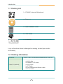
1
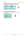
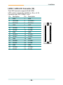
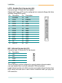
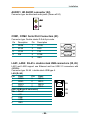
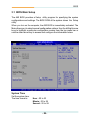
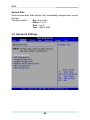
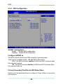
IP-M45A1
Mini ITX Industrial Motherboard
User’s Manual
Version 1.0
2008.09
This page is intentionally left blank.
Index
Table of Contents
Chapter 1 - Introduction............................................ 1
1.1 Copyright Notice .......................................................2
1.2 About this User’s Manual .........................................2
1.3 Warning......................................................................2
1.4 Replacing the lithium battery...................................3
1.5 Technical Support .....................................................3
1.6 Warranty.....................................................................4
1.7 Packing List...............................................................5
1.8 Ordering Information ................................................5
6SHFL¿FDWLRQV............................................................6
1.10 Board Dimensions ..................................................7
1.11 Installing the CPU ...................................................8
1.12 Installing the Memory .............................................9
Chapter 2 - Installation............................................ 11
2.1 Block Diagram.........................................................12
2.2 Jumpers and Connectors.......................................13
Jumpers ..........................................................................14
JBAT1: Clear CMOS Setup.............................................14
JRS1: COM2 RS-232/422/485 Select .............................15
JVLCD1: LCD Panel Voltage Select ..............................15
JV1: COM port Power Special Support ........................16
JPWR1: AT/ATX Power Mode.........................................16
Connectors .....................................................................17
CPUF1: CPU Fan Power Connector..............................17
SATA1 ~4: Serial ATA Connectors.................................17
DIO1: Digital I/O Connector ...........................................17
USB1/ USB2: USB Connectors......................................18
SYSF1: System Fan Power Connector .........................18
PCI1: 32-bit PCI Slot .......................................................19
MiniPCI1: MiniCPI socket...............................................21
TV1: TV-out Connector...................................................21
CON1: RS-422/ 485 Output Connector .........................23
-i-
Index
INV1: LCD Inverter Connector.......................................23
LVDS1: LVDS LCD COnnector.......................................24
LPT1: Parallel Port Connector.......................................25
IR1: Infrared Connector .................................................25
AUDIO1: HD Audio Connector.......................................26
COM1, COM2: Serial Port Connectors..........................26
LAN1, LAN2: RJ-45 + double stack USB connectors.26
VGA1: CRT & DVI-D Connectors...................................27
J1: HDMI Connector .......................................................28
EKB1: External Keyboard & Mouse Connector ...........28
PW1: ATX Power Connector ..........................................29
2.3 The Installation Paths of CD Driver.......................30
Chapter 3 - BIOS ...................................................... 31
3.1 BIOS Main Setup .....................................................32
3.2 Advanced Settings..................................................33
&38&RQ¿JXUDWLRQ ..............................................34
,'(&RQ¿JXUDWLRQ ................................................35
)ORSS\&RQ¿JXUDWLRQ ..........................................36
6XSHU,2&RQ¿JXUDWLRQ .......................................37
+DUGZDUH+HDOWK&RQ¿JXUDWLRQ...........................39
$+&,&RQ¿JXUDWLRQ ..............................................40
86%&RQ¿JXUDWLRQ ..............................................41
3.3 Advanced PCI/PnP Settings..................................42
3.4 Boot Settings...........................................................43
%RRW6HWWLQJV&RQ¿JXUDWLRQ.................................44
3.4.2 Boot device Priority...............................................45
3.5 Security....................................................................46
3.6 Advanced Chipset Settings....................................48
1RUWK%ULGJH&KLSVHW&RQ¿JXUDWLRQ...................48
6RXWK%ULGJH&KLSVHW&RQ¿JXUDWLRQ ..................50
3.7 Exit Options.............................................................52
3.8 Beep Sound codes list ...........................................57
3.8.1 Boot Block Beep codes .......................................57
- ii -
Index
3.8.2 POST BIOS Beep codes.......................................57
3.8.3 Troubleshooting POST BIOS Beep codes..........58
3.9 AMI BIOS Checkpoints ...........................................59
3.9.1 Bootblock Initialization Code Checkpoints........59
3.9.2 Bootblock Recovery Code Checkpoints ............61
3.9.3 POST Code Checkpoints .....................................63
3.9.4 DIM Code Checkpoints ........................................67
3.9.5 ACPI Runtime Checkpoints .................................69
Chapter 4 - Appendix .............................................. 70
4.1 I/O Port Address Map..............................................71
4.2 Interrupt Request Lines (IRQ)................................72
4.3 BIOS memory mapping ..........................................73
- iii -
Index
This page is intentionally left blank.
- iv -
Introduction
1
Chapter 1
Introduction
Chapter 1 - Introduction
-1-
Introduction
1.1 Copyright Notice
All Rights Reserved.
The information in this document is subject to change without prior notice in
order to improve the reliability, design and function. It does not represent a
commitment on the part of the manufacturer.
Under no circumstances will the manufacturer be liable for any direct, indirect,
special, incidental, or consequential damages arising from the use or inability
to use the product or documentation, even if advised of the possibility of such
damages.
This document contains proprietary information protected by copyright.
All rights are reserved. No part of this manual may be reproduced by any
mechanical, electronic, or other means in any form without prior written
permission of the manufacturer.
1.2 About this User’s Manual
This User’s Manual is intended for experienced users and integrators with
hardware knowledge of personal computers. If you are not sure about any
description in this User’s Manual, please consult your vendor before further
handling.
1.3 Warning
Single Board Computers and their components contain very delicate
Integrated Circuits (IC). To protect the Single Board Computer and its
components against damage from static electricity, you should always follow
the following precautions when handling it :
1. Disconnect your Single Board Computer from the power source when you
want to work on the inside.
2. Hold the board by the edges and try not to touch the IC chips, leads or
circuitry.
3. Use a grounded wrist strap when handling computer components.
4. Place components on a grounded antistatic pad or on the bag that came
with the Single Board Computer, whenever components are separated
from the system.
-2-
Introduction
1.4 Replacing the lithium battery
Incorrect replacement of the lithium battery may lead to a risk of explosion.
The lithium battery must be replaced with an identical battery or a battery type
recommended by the manufacturer.
Do not throw lithium batteries into the trashcan. It must be disposed of in
accordance with local regulations concerning special waste.
1.5 Technical Support
,I \RX KDYH DQ\ WHFKQLFDO GLI¿FXOWLHV SOHDVH FRQVXOW WKH XVHU¶V PDQXDO ¿UVW
in Driver CD
Please do not hesitate to call or e-mail our customer service when you still can
QRW¿QGRXWWKHDQVZHU
http://www.IPOXUSA.com
E-mail:[email protected]
-3-
Introduction
1.6 Warranty
This product is warranted to be in good working order for a period of two years
from the date of purchase. Should this product fail to be in good working order
at any time during this period, we will, at our option, replace or repair it at no
additional charge except as set forth in the following terms. This warranty
GRHV QRW DSSO\ WR SURGXFWV GDPDJHG E\ PLVXVH PRGL¿FDWLRQV DFFLGHQW RU
disaster.
9HQGRUDVVXPHVQROLDELOLW\IRUDQ\GDPDJHVORVWSUR¿WVORVWVDYLQJVRUDQ\
other incidental or consequential damage resulting from the use, misuse of,
or inability to use this product. Vendor will not be liable for any claim made by
any other related party.
Vendors disclaim all other warranties, either expressed or implied, including
EXW QRW OLPLWHG WR LPSOLHG ZDUUDQWLHV RI PHUFKDQWLELOLW\ DQG ¿WQHVV IRU D
particular purpose, with respect to the hardware, the accompanying product’s
manual(s) and written materials, and any accompanying hardware. This
OLPLWHGZDUUDQW\JLYHV\RXVSHFL¿FOHJDOULJKWV
Return authorization must be obtained from the vendor before returned
merchandise will be accepted. Authorization can be obtained by calling or
faxing the vendor and requesting a Return Merchandise Authorization (RMA)
number. Returned goods should always be accompanied by a clear problem
description.
-4-
Introduction
1.7 Packing List
1 x IP-M45A1 Industrial Motherboard
1 x Driver CD
1 x Quick Installation Guide
1 x CPU Cooler
1 x I/O bracket
If any of the above items is damaged or missing, contact your vendor
immediately.
1.8 Ordering Information
IP-M45A1
Cable Kit (optional)
IP-M45A1 Mini-ITX industrial motherboard w/ dual LAN
1 x USB Cable
1 x Parallel to FDD Cable
1 x SATA Cable
1 x LPT Cable
1 x PS/2 Keyboard and Mouse Cable
1 x TV-out Cable
-5-
Introduction
6SHFL¿FDWLRQV
Form Factor
Mini-ITX industrial motherboard
CPU
mPGA 478 Socket for Intel® Penryn dual core and Penryn
single core CPU
Chipset
Intel® GM45 + Intel® ICH9M
System Memory
2 x 240-pin DIMM socket Up to 4GB DDR II SDRAM
667/800MHz
VGA/ LCD Controller
Mobile Intel® Graphics Media Accelerator 4500MHD
graphics core w/ CRT/ Dual Channel LVDS/ TV-Out
Ethernet
2 x Realtek 8111B PCIe 10/100/1000 Base-T Fast
Ethernet LAN
I/O Chips
Winbond W83627HG
BIOS
AMI PnP Flash BIOS
Audio
Realtek ALC888HD Audio Codec, MIC-in/Line-In/LineOut, 7.1 channels (Default w/o Line-In)
Serial ATA
4 x Serial ATA (300MB/s)
Serial Port
2 x COM port (COM1: RS-232, COM2: RS-232/422/485
selectable)
Parallel Port/ Floppy
1 x LPT Port (SPP/EPP/ECP mode selectable)
1 x Floppy connector, shared with Parallel Port #1
KBMS
Standard PS/2 Keyboard and Mouse
Universal Serial Bus
8 x USB 2.0 compliant
DIO
8-bit programmable Digital Input/Output
Expansion Interface
1 x PCI slot
1 x Mini PCI Socket
Operation Temp.
-20oC ~ 70oC (-4oF ~ 158oF)
Watchdog Timer
255-level Reset
Dimension (L x W)
170 x 170 mm (6.7” x 6.7”)
-6-
Introduction
1.10 Board Dimensions
34.8
CPU Cooler
6.33
NB Heat Sink
170.00
10.16
33.02
1
154.94
132.08
CPU Cooler
mPGA478B
157.48
169.98
LAN2
LAN1
COM1
Line Out
COM2
Mic
26.00
VGA
HDMI
DVI
USB
USB
9.78
43.98
74.85
22.07
123.78
24.23
Unit: mm
162.16
-7-
31.10
Introduction
1.11 Installing the CPU
The processor socket comes with a screw to secure the CPU. As showing in
WKHSLFWXUHDVEHOORZORRVHWKHVFUHZ¿UVWEHIRUHLQVHUWLQJWKH&38
Place the CPU into the socket by making sure the notch on the corner of the
CPU corresponding with the notch on the inside of the socket. Once the CPU
has slide into the socket, lock the screw.
Make sure that heat sink of the CPU top surface is in complete contact to
avoid the CPU overheating problem.
If not, it would cause your system or CPU to be hanged, unstable, damaged.
-8-
Introduction
1.12 Installing the Memory
To install the Memory module, locate the Memory DIMM slot on the board and
perform as below:
1. Hold the Memory module so that the key of the Memory module align
with those on the Memory DIMM slot.
2. Gently push the Memory module in an upright position and a right way until
the clips of the DIMM slot close to lock the Memory module in place, when
the Memory module touches the bottom of the DIMM slot.
3. To remove the Memory module, just pressing the clips of DIMM slot with
both hands.
Lock
Lock
-9-
Introduction
This page is intentionally left blank.
- 10 -
Installation
2
Chapter 2
Installation
Chapter 2 - Installation
- 11 -
Installation
2.1 Block Diagram
Socket 478
for Intel®
Penryn
FSB
VGA
Analog
R.G.B.
Intel®
GM45
LVDS
TV-Out
HDMI
DVI
2 x 240-pin DDR II
DIMM socket
Memory Bus
667/800MHz
DMI I/F
8 x USB
4 x SATA
1 x MiniPCI Socket
USB I/F
Serial ATA I/F
Intel®
ICH9M
LAN
Controller
LPC I/F
PCIe x1
Audio
1 x PCI Slot
PCI Bus
HD
Codec
Super IO
Controller
COM1
COM2
LPT1/
FDD
KB
MS
- 12 -
IrDA
8-bit
DIO
2 x RJ-45
100/1000 Base-T
Installation
2.2 Jumpers and Connectors
CPUF1 SATA3, SATA4
1
DIMM2
2
DIO1
3
4
SATA1, SATA2
DIMM1
5
6
9
1
10
2
1
1
1
1
10
9
2
1
10
9
1
mPGA478B
7
USB1
8
1
2
1
DIMM2,
DIMM1
USB2
JBAT1
9
SYSF1
10
1
32
123
124
PCI1
JPWR1
31
11
1
MINIPCI1
1
11
TV1
PW1
2
20
6
2 5
1
1
2
30
1
1
29
13
26
14
JRS1
15
CON1
16
INV1
LVDS1
18
17
1
1
14
JVLCD1 19
LPT1 20
1
EKB1
29
JFRT1
2
1 1
1
10
1
30
13
1
1
J1
VGA1
LAN2
28
27
26
LAN1 JV1
25
- 13 -
24
COM2
COM1
23
AUDIO1
22
IR1
21
12
Installation
Jumpers
JBAT1: Clear CMOS Setup (9)
If the board refuses to boot due to inappropriate CMOS settings here is how
to proceed to clear (reset) the CMOS to its default values.
Connector type: 2.54 mm pitch 1x3 pin header
Pin
Mode
1-2
Keep CMOS (Default)
2-3
Clear CMOS
3
2
1
3
2
1
You may need to clear the CMOS if your system cannot boot up because you
forgot your password, the CPU clock setup is incorrect, or the CMOS settings
need to be reset to default values after the system BIOS has been updated.
Refer to the following solutions to reset your CMOS setting:
Solution A:
1. Power off the system and disconnect the power cable.
3ODFHDVKXQWWRVKRUWSLQDQGSLQRI-%$7IRU¿YHVHFRQGV
3. Place the shunt back to pin 2 and pin 3 of JBAT1.
4. Power on the system.
Solution B:
If the CPU Clock setup is incorrect, you may not be able to boot up. In this
case, follow these instructions:
1. Turn the system off, then on again. The CPU will automatically boot up
using standard parameters.
2. As the system boots, enter BIOS and set up the CPU clock.
Note:
If you are unable to enter BIOS setup, turn the system on and off a few
times.
- 14 -
Installation
JRS1: COM2 RS-232/422/485 Select (15)
7KHRQERDUG&20SRUWFDQEHFRQ¿JXUHGWRRSHUDWHLQ56RU56
modes. RS-422 modes differ in the way RX/TX is being handled. Jumper JRS1
switches between RS-232 or RS-422/485 mode. When JRS1 is set to RS-422
or RS-485 mode, there will be only +12V output let while JRS1 is set.
All RS-232/422/482 modes are available on COM2.
,WFDQEHFRQ¿JXUHG&20WRRSHUDWHLQ5656RU56PRGH
Connector type: 2.00mm pitch 2x3 pin header.
Mode
RS-232 (Default)
RS-422
RS-485
1-2
ON
OFF
OFF
3-4
OFF
ON
OFF
5-6
OFF
OFF
ON
1
2
1
2
1
2
5
6
5
6
5
6
JVLCD1: LCD Panel Voltage Select (19)
The voltage of LCD panel could be selected by JVLCD1 in +5V or +3.3V.
Connector type: 2.54 mm pitch 1x3 pin header
Pin
Voltage
1-2
+5V
2-3
+3.3V (Default)
- 15 -
3
2
1
3
2
1
Installation
JV1: COM port Power Special Support (24)
The COM1 port’s voltage could be selected by LV1 respectively to +5V.
Connector type: 2.54mm pitch 1x3 pin header.
Pin
Setup
1-2
Standard signal for Pin-9. (Default)
2-3
+5V
3
2
1
3
2
1
JPWR1: AT/ATX Power Mode (31)
The power mode jumper selects the power mode for the system.
Connector type: 2.54mm pitch 1x2 pin header.
Pin 1-2
Mode
Short
AT Mode
1
2
Open
ATX Mode (Default)
1
2
- 16 -
Installation
Connectors
CPUF1: CPU Fan Power Connector (1)
CPUF1 is 3-pin header for the system fan. The fan must be a +12V fan.
Pin
Description
1
GND
1
2
+12V
3
3
FAN_Detect
2
SATA1~ 4: Serial ATA Connectors (2, 3, 5, 6)
The IP-M45A1 on board supports four SATA connectors, second generation
SATA drives transfer data at speeds as high as 300MB/s, twice the transfer
VSHHGRI¿UVWJHQHUDWLRQ6$7$GULYHV7KH6$7$GULYHVFDQEHFRQ¿JXUHGLQD
5$,'5$,'RU5$,'FRQ¿JXUDWLRQ
Pin
Description
1
GND
2
TX+
3
TX-
4
GND
5
RX-
6
RX+
7
GND
1
7
DIO1: Digital I/O Connector (4)
DIO1 is a 8-bit DIO connector that supports 4-bit In/ 4-bit Out.
Connector type: 2.54 mm pitch 2x5 pin header.
Pin
Description
Pin
Description
1
DIO1
2
DIO2
3
DIO3
4
DIO4
5
DIO5
6
DIO6
7
DIO7
8
DIO8
9
+5V
10
GND
- 17 -
Installation
USB1, USB2: USB Connectors (7, 8)
The IP-M45A1 CPU board on board supports three headers USB1 and USB2
that can connect up to six high-speed (Data transfers at 480MB/s), full-speed
(Data transfers at 12MB/s) or low-speed (Data transfers at 1.5MB/s) USB
devices.
Connector type: 2.00mm 2x5 pin header
Pin
Description
Pin
Description
1
+5V
2
+5V
3
USBD-
4
USBD-
5
USBD+
6
USBD+
7
GND
8
GND
9
N/C (Key)
10
N/C
1
2
9
10
SYSF1: Systen Fan Power Connector (10)
SYSF1 is 3-pin header for the system fan. The fan must be a +12V fan.
Pin
Description
1
GND
1
2
+12V
3
3
FAN_Detect
2
- 18 -
Installation
PCI1: 32-bit PCI Slot (11)
Pin
B1
B2
B3
B4
B5
B6
B7
B8
B9
B10
B11
B12
B13
B14
B15
B16
B17
B18
B19
B20
B21
B22
B23
B24
B25
B26
B27
B28
B29
B30
B31
B32
B33
B34
Description
-12V
TCK
GND
TDO
+5V
+5V
INTB#
INTD#
PRSTN1
RSVD
PRSTN2
GND
GND
RSVD
GND
CLK
GND
REQ#
+5V
AD31
AD29
GND
AD27
AD25
+3.3V
C/BE3#
AD23
GND
AD21
AD19
+3.3V
AD17
C/BE2#
GND
Pin
A1
A2
A3
A4
A5
A6
A7
A8
A9
A10
A11
A12
A13
A14
A15
A16
A17
A18
A19
A20
A21
A22
A23
A24
A25
A26
A27
A28
A29
A30
A31
A32
A33
A34
- 19 -
Description
TRST
+12V
TMS
TDI
+5V
INTA#
INTC#
+5V
RSVD
+5V
RSVD
GND
GND
3.3V_AUX
RST#
+5V
GNT#
GND
PME#
AD30
+3.3V
AD28
AD26
GND
AD24
IDSEL
+3.3V
AD22
AD20
GND
AD18
AD46
+3.3V
FRAME#
Installation
B35
B36
B37
B38
B39
B40
B41
B42
B43
B44
B45
B46
B47
B48
B49
B52
B53
B54
B55
B56
B57
B58
B59
B60
B61
B62
IRDY#
+3.3V
DEVSEL#
GND
LOCK#
PERR#
+3.3V
SERR#
+3.3V
C/BE1#
AD14
GND
AD12
AD10
GND
AD6
AD7
+3.3V
AD5
AD3
GND
AD1
+5V
ACK64#
+5V
+5V
A35
A36
A37
A38
A39
A40
A41
A42
A43
A44
A45
A46
A47
A48
A49
A52
A53
A54
A55
A56
A57
A58
A59
A60
A61
A62
- 20 -
GND
TRDY#
GND
STOP#
+3.3V
SDONE
SBO#
GND
PAR
AD15
+3.3V
AD13
AD11
GND
AD9
C/BE0#
+3.3V
AD6
AD4
GND
AD2
AD0
+5V
REQ64#
+5V
+5V
Installation
MINIPCI1: MiniPCI socket (12)
TV1: TV Out Connector (13)
The TV out connector is for output to a television.
Connector type: 2.00mm pitch 1x6-pin box wafer connector
Composite Video
CVBS
1
2
GND
3
Unused
4
GND
5
Unused
6
GND
S-Video
Unused
1
2
GND
3
Luminance
4
GND
5
Chrominance
6
GND
2
GND
Component Video
Pb
1
3
Y
4
GND
5
Pr
6
GND
- 21 -
1
2
3
4
5
6
Installation
JFRT1: Switches and Indicators (14)
It provides connectors for system indicators that provides light indication of
the computer activities and switches to change the computer status.
Connector type: 2.54 mm pitch 2x8 pin header
Pin
Description
Pin
Description
1
Power LED+
2
PWRBTN-
3
GND
4
PWRBTN+
5
GND
6
RESET+
7
HDD LED+
8
RESET-
9
HDD LED-
10
SPEAKER+
11
SMBCLK
12
SPEAKER+
13
SMBDATA
14
SPEAKER-
15
GND
16
SPEAKER-
1 2
15 16
PLED: Power LED Connector, pin 1-3.
This 2-pin connector connects to the case-mounted power LED. Power LED can be
indicated when the CPU card is on or off. And keyboard lock can be used to disable
the keyboard function so the PC will not respond by any input.
HLED: HDD LED Connector, pin 7-9.
This 2-pin connector connects to the case-mounted HDD LED to indicate hard disk
activity.
SM Bus: SM Bus connector, pin 11, 13, 15.
PWRBTN: ATX soft power switch, pin 2-4.
This 2-pin connector connects to the case-mounted Power button.
RES: Reset Button, pin 6-8.
This 2-pin connector connects to the case-mounted reset switch and is used to
reboot the system.
SPK: External Speaker, pin 10, 12, 14, 16.
This 4-pin connector connects to the case-mounted speaker.
- 22 -
Installation
CON1: RS-422/ 485 Output Connector (16)
Connector type: 2.00mm pitch 1x4 box wafer connector
Pin
RS-422
RS-485
1
TX+
Data+
2
TX-
Data-
3
RX+
N/C
4
RX-
N/C
1
2
3
4
INV1: LCD Inverter Connector (17)
Connector type: 2.00mm pitch 1x5-pin box wafer connector.
Pin
Description
1
+12V
2
GND
3
Backlight on/off
4
N/C
5
GND
1
2
3
4
5
- 23 -
Installation
LVDS1: LVDS LCD Connector (18)
The LVDS connector supports 24-bit LVDS.
VDD could be selected by JVLCD1 in +5V or +3.3V.
Connector type: DF-13-30DP-1.25V
Pin
Description
Pin
Description
2
VDD
1
VDD
4
TX2CLK+
3
TX1CLK+
6
TX2CLK-
5
TX1CLK-
8
GND
7
GND
10
TX2D0+
9
TX1D0+
12
TX2D0-
11
TX1D0-
14
GND
13
GND
16
TX2D1+
15
TX1D1+
18
TX2D1-
17
TX1D1-
20
GND
19
GND
22
TX2D2+
21
TX1D2+
24
TX2D2-
23
TX1D2-
26
GND
25
GND
28
TX2D3+
27
TX1D3+
30
TX2D3-
29
TX1D3-
- 24 -
2
1
30
29
Installation
LPT1: Parallel Port Connector (20)
Connector type: 2.00 pitch 2x13 pin header.
6KDUHGZLWK)ORSS\/37FDQEHFRQ¿JXUHGDVDFRQQHFWRUÀRSS\GLVNGULYH
interface through BIOS setup.
Pin
Description
Pin
Description
1
STROBE
14
AFD
2
PTD0
15
ERROR
3
PTD1
16
INIT
4
PTD2
17
SLIN
5
PTD3
18
GND
6
PTD4
19
GND
7
PTD5
20
GND
8
PTD6
21
GND
9
PTD7
22
GND
10
ACK
23
GND
11
BUSY
24
GND
12
PE
25
GND
13
SELECT
26
N/C
1 14
13 26
IR1: Infrared Connector (21)
Connector type: 2.54mm pitch 1x5 pin header
Pin
Description
1
+5V
2
N/C
3
IRRX
4
GND
1
2
3
4
5
5
IRTX
7KH,5FRQQHFWRUFDQEHFRQ¿JXUHGWRVXSSRUWZLUHOHVVLQIUDUHGPRGXOH
XVHUFDQWUDQVIHU¿OHVWRRUIURPQRWHERRNV3'$DQGSULQWHUV
Install infrared module onto IrDA connector and enable infrared function from
BIOS setup and make sure to have correct orientation when you plug onto
IrDA connector.
- 25 -
Installation
AUDIO1: HD AUDIO connector (22)
Connector type: double stack audio jacks (Stereo ø3.50).
ren:LineutO
G
nk:P
i ciM
COM1, COM2: Serial Port Connectors (23)
Connector type: Double stacks D-Sub 9-pin male.
Pin
Description
6
DSR#
1
DCD#
7
RTS#
2
RXD
8
CTS#
3
TXD
9
RI#
4
DTR#
5
GND
1
9
1
5
5
6
Description
6
Pin
9
LAN1, LAN2: RJ-45 + double stack USB connectors (25, 26)
LAN1 and LAN2 support one Ethernet and two USB 2.0 connectors with
480MB/s.
Connector type: RJ-45 + double stack USB type A.
LAN (RJ-45)
Pin
Desc.
Pin
Desc.
1
MDI0+
5
MDI2+
2
MDI06
MDI2LAN
3
MDI1+
7
MDI3+
4
MDI18
MDI3USB
USB (USB type A connector)
Pin
Desc.
USB
1
+5V
2
USB3
USB+
4
GND
LED
LED
87654321
1 2 3 4
1 2 3 4
- 26 -
Installation
VGA1: CRT & DVI-D Connectors (27)
Connector type: VGA: D-Sub 15-pin female.
DVI-D: DVI-D female.
5
1
15
11
1
8
17
24
CRT
DVI-D
CRT Connector
Pin
Description
Pin
Description
Pin
Description
1
RED
6
GND
11
N/C
2
GREEN
7
GND
12
VDDAT
3
BLUE
8
GND
13
HSYNC
4
N/C
9
+5V
14
VSYNC
5
GND
10
GND
15
VDCLK
DVI-D Connector
Pin
Description
Pin
Description
Pin
Description
1
TMDS Data 2-
9
TMDS Data 1-
17
TMDS Data 0-
2
TMDS Data 2+
10
TMDS Data 1+
18
TMDS Data 0+
3
TMDS Data 2/4
shield
11
TMDS Data 1/3
shield
19
TMDS Data 0/5
shield
4
TMDS Data 4-
12
TMDS Data 3-
20
TMDS Data 5-
5
TMDS Data 4+
13
TMDS Data 3+
21
TMDS Data 5+
6
DDC clock
14
+5V
22
TMDS Data
clock shield
7
DDC data
15
GND
23
TMDS clock+
8
Analog vertical
sync
16
Hot plug detect
24
TMDS clock-
- 27 -
Installation
J1: HDMI Connector (28)
Connector type: HDMI 19-pin female.
2
18
1
19
Pin
Desc.
Pin
Desc.
1
HDMI_DATA2
2
GND
3
HDMI_DATA2#
4
HDMI_DATA1
5
GND
6
HDMI_DATA1#
7
HDMI_DATA0
8
GND
9
HDMI_DATA0#
10
HDMI_CLK
11
GND
12
HDMI_CLOK2
13
N/C
14
N/C
15
HDMI_SPD
16
HDMI_SPC
17
GND
18
+5V
19
HDMI_HTPLG
EKB1: External Keyboard & Mouse Connector (29)
Connector type: 2.54mm pitch 1x6-pin box wafer connector
Pin
Description
1
KB Data
2
GND
3
MS Data
4
KB Clock
5
+5V
6
MS Clock
1
6
- 28 -
Installation
PW1: ATX Power Supply Connector (30)
The ATX power supply has a single lead connector with a clip on one side
of the plastic housing. There is only one way to plug the lead into the ATX
power connector. Press the lead connector down until the clip snaps into
place and secures the lead onto the connector.
Pin Description Pin Description
11
+3.3V
1
+3.3V
12
-12V
2
+3.3V
13
GND
3
GND
14
PS-ON
4
+5V
15
GND
5
GND
16
GND
6
+5V
17
GND
7
GND
18
-5V
8
PW-OK
19
+5V
9
+5VSB
20
+5V
10
+12V
11
1
20
10
Warning
Incorrect installation of the power supply could result in serious damage to
the mainboard and connected peripherals. Make sure the power supply is
unplugged from the AC outlet before connecting the leads from the power
supply.
- 29 -
Installation
2.3 The Installation Paths of CD Driver
Windows 2000 & XP
Driver
Path
AUDIO
\Realtek_HD\Windows_R198\WDM_198
CHIPSET ?,QWHO?,1)?LQ¿QVWBDXWRO
LAN
\Realtek\8111B_WIN5698\Setup
VGA
\Intel_2K_XP_32\1434\WINXP_14344
\Intel_2K_XP_64\1434\WINXP64_14344
Windows Vista
Driver
Path
AUDIO
\Realtek_HD\Vista_6206_0619\Setup
CHIPSET ?,QWHO?,1)?LQ¿QVWBDXWRO
LAN
\Realtek\8111B_Vista_R198\Vista_R198
VGA
\Intel_Vista_32\1598\WinVista_1598
\Intel_Vista_64\1598\WinVista64_1598
- 30 -
BIOS
3
Chapter 3
BIOS
Chapter 3 - BIOS
- 31 -
BIOS
3.1 BIOS Main Setup
The AMI BIOS provides a Setup utility program for specifying the system
FRQ¿JXUDWLRQVDQGVHWWLQJV7KH%,26520RIWKHV\VWHPVWRUHVWKH6HWXS
utility.
When you turn on the computer, the AMI BIOS is immediately activated. The
0DLQDOORZV\RXWRVHOHFWVHYHUDOFRQ¿JXUDWLRQRSWLRQV8VHWKHOHIWULJKWDUURZ
NH\VWRKLJKOLJKWDSDUWLFXODUFRQ¿JXUDWLRQVFUHHQIURPWKHWRSPHQXEDURU
XVHWKHGRZQDUURZNH\WRDFFHVVDQGFRQ¿JXUHWKHLQIRUPDWLRQEHORZ
System Time
Set the system time.
The time format is:
Hour : 00 to 23
Minute : 00 to 59
Second : 00 to 59
- 32 -
BIOS
System Date
Set the system date. Note that the ‘Day’ automatically changes when you set
the date.
The date format is:
Day : Sun to Sat
Month : 1 to 12
Date : 1 to 31
Year : 1999 to 2099
3.2 Advanced Settings
- 33 -
BIOS
&38&RQ¿JXUDWLRQ
7KH&38&RQ¿JXUDWLRQVHWXSVFUHHQYDULHVGHSHQGLQJRQWKHLQVWDOOHG
processor.
Execute Disable Bit
:KHQGLVDEOHGIRUFHWKH6'IHDWXUHÀDJWRDOZD\VUHWXUQ
- 34 -
BIOS
,'(&RQ¿JXUDWLRQ
6$7$&RQ¿JXUDWLRQ
(QDEOH(QDEOH6$7$FRQ¿JXUDWLRQ
'LVDEOHG'LVDEOH6$7$FRQ¿JXUDWLRQ
&RQ¿JXUH6$7$DV
This BIOS feature controls the SATA controller’s operating mode.
There are two available modes - IDE and RAID. When set to:
RAID - the SATA controller enables its RAID and AHCI functions when
the computer boots up.
IDE - the SATA controller disables its RAID and AHCI functions when
the computer boots up.
Primary/Secondary/Third/Fourth IDE Master/Slave
6HOHFWRQHRIWKHKDUGGLVNGULYHVWRFRQ¿JXUHLW3UHVV(QWHU!WRDFFHVVLWV
the sub menu.
- 35 -
BIOS
)ORSS\&RQ¿JXUDWLRQ
6HOHFWWKHW\SHRIÀRSS\GLVNGULYHLQVWDOOHGLQ\RXUV\VWHP
The choice:
None
360K 5.25”
1.2M 5.25”
720K 3.5”
1.44M 3.5”
2.88M 3.5”
Floppy 3: The choice are Disabled or Enabled.
- 36 -
BIOS
6XSHU,2&RQ¿JXUDWLRQ
Serial Port1 / Port2 Address
6HOHFWDQDGGUHVVDQGFRUUHVSRQGLQJLQWHUUXSWIRUWKH¿UVWDQGVHFRQGVHULDO
ports.
The choice:
3F8/IRQ4
2E8/IRQ3
3E8/IRQ4
2F8/IRQ3
Disabled
Auto
Serial Port2 Mode
Allows BIOS to select mode for serial Port2.
- 37 -
BIOS
Parallel Port Address
Select an address for the parallel port.
The choice:
3BC
378
278
Disabled
Parallel Port Mode
Select an operating mode for the onboard parallel port. Select Normal,
Compatible or SPP unless you are certain your hardware and software both
support one of the other available modes.
The choice:
SPP
EPP
ECP
ECP + EPP
Normal
Parallel Port IRQ
Select an interrupt for the parallel port.
The choice:
IRQ5
IRQ7
- 38 -
BIOS
+DUGZDUH+HDOWK&RQ¿JXUDWLRQ
System/ CPU Temperature
Show you the current System / CPU fan temperature.
CPU Fan Speed
Show you the current CPU Fan operating speed.
Vcore
Show you the voltage level of CPU (Vcore).
+1.5V / +3.3Vin / +5Vin / +12Vin / 5VSB
Show you the voltage level of the +1.5V, +3.3Vin, +5Vin, +12Vin and +5V
standby.
- 39 -
BIOS
$+&,&RQ¿JXUDWLRQ
AHCI Port 0 / Port 1 / Port 2/ Port 3
While entering setup, BIOS auto detects the presence of IDE devices. This
displays the status of auto detection of IDE devices.
- 40 -
BIOS
86%&RQ¿JXUDWLRQ
ACPI Function
,WVXSSRUWV$&3,$GYDQFH&RQ¿JXUDWLRQDQG3RZHU,QWHUIDFH
Setting: Enabled (Default), Disabled.
Legacy USB Support
Enables support for legacy USB. AUTO option disables legacy support if no
USB devices are connected.
USB 2.0 Controller Mode
&RQ¿JXUHVWKH86%FRQWUROOHULQ+LJK6SHHG0ESVRU)XOO6SHHG
(12MBPS).
BIOS EHCI Hand-Off
This is a work around for OSs without EHCI hand-Off support. The EHCI
ownership change should claim by EHCI driver.
86%0DVV6WRUDJH'HYLFH&RQ¿JXUDWLRQ
- 41 -
BIOS
3.3 Advanced PCI/PnP Settings
Plug & Play O/S
1R/HWVWKH%,26FRQ¿JXUHDOOWKHGHYLFHVLQWKHV\VWHP
<HV OHWV WKH RSHUDWLQJ V\VWHP FRQ¿JXUH 3OXJ DQG 3OD\ 3Q3 GHYLFHV
not required for BOOT if your system has a Plug and Play operating
system.
PCI Latency Timer
Value in units of PCI clocks for PCI device latency timer register.
Allocate IRQ to PCI VGA
Yes: Assigns IRQ to PCI VGA card if card requests IRQ.
No: Does not assign IRQ to PCI VGA card even if card requests an IRQ.
- 42 -
BIOS
3.4 Boot Settings
Boot Device Priority
Press Enter and it shows Bootable add-in devices.
Removable Drives
Press Enter and it shows Bootable and Removable drives.
- 43 -
BIOS
%RRW6HWWLQJV&RQ¿JXUDWLRQ
Bootup Num-Lock
6HWWKLVYDOXHWRDOORZWKH1XPEHU/RFNVHWWLQJWREHPRGL¿HGGXULQJERRW
up.
PS/2 Mouse Support
Interrupt 19 capture
Enabled: Allows option ROMs to trap interrupt 19. This is required by some
PCI cards that provide a ROM based setup utility.
LAN Boot Function
Set this option to LAN add-on Boot ROM function.
- 44 -
BIOS
3.4.2 Boot device Priority
1st/ 2nd/ 3rd Boot Device
6SHFL¿HVWKHERRWVHTXHQFHIRUPWKHDYDLODEOHGHYLFHV
A device enclosed in parenthesis has been disabled in the corresponding type
menu.
- 45 -
BIOS
3.5 Security
Auto Detect PCI Clk
It enables or disables the auto detection of the PCI clock.
Setting: Enabled (Default), Disabled.
Supervisor Password & User Password
You can set either supervisor or user password, or both of then.
The differences between are:
Set Supervisor Password: Can enter and change the options of the
setup menus.
Set User Password: Just can only enter but do not have the right to
change the options of the setup menus. When you select this function, the
following message will appear at the center of the screen to assist you in
creating a password.
ENTER PASSWORD:
- 46 -
BIOS
7\SHWKHSDVVZRUGXSWRHLJKWFKDUDFWHUVLQOHQJWKDQGSUHVV(QWHU!
The password typed now will clear any previously entered password from
&026PHPRU\<RXZLOOEHDVNHGWRFRQ¿UPWKHSDVVZRUG7\SHWKHSDVVZRUG
DJDLQDQGSUHVV(QWHU!<RXPD\DOVRSUHVV(6&!WRDERUWWKHVHOHFWLRQ
and not enter a password.
7R GLVDEOH D SDVVZRUG MXVW SUHVV (QWHU! ZKHQ \RX DUH SURPSWHG WR
HQWHU WKH SDVVZRUG$ PHVVDJH ZLOO FRQ¿UP WKH SDVVZRUG ZLOO EH GLVDEOHG
Once the password is disabled, the system will boot and you can enter Setup
freely.
PASSWORD DISABLED.
When a password has been enabled, you will be prompted to enter it
every time you try to enter Setup. This prevents an unauthorized person from
FKDQJLQJDQ\SDUWRI\RXUV\VWHPFRQ¿JXUDWLRQ
Additionally, when a password is enabled, you can also require the BIOS
to request a password every time your system is rebooted. This would prevent
unauthorized use of your computer.
You determine when the password is required within the BIOS Features
Setup Menu and its Security option. If the Security option is set to “System”,
the password will be required both at boot and at entry to Setup. If set to
“Setup”, prompting only occurs when trying to enter Setup.
- 47 -
BIOS
3.6 Advanced Chipset Settings
1RUWK%ULGJH&KLSVHW&RQ¿JXUDWLRQ
Boots Graphic Adapter Priority
Select which graphics controller to use as the primary boot device.
Internal Graphic Mode Select
Select the amount of system memory used by the Internal graphics device.
3(*3RUW&RQ¿JXUDWLRQ
This item allows you to control the PEG or on-chip VGA.
The Choice: Auto, Disabled.
- 48 -
BIOS
9LGHR)XQFWLRQ&RQ¿JXUDWLRQ
DVMT Mode
The choice: FIXED, DVMT (Default), Both.
Boot Display Device
Setting: CRT, LVDS, CRT+ LVDS (Default).
Flat Panel Type
It allows you to select the Flat Panel type as below --Setting:
640x480
800x600
1024x768
(Default)
1280x1024
1400x1050
1400x1050
1600x1200
1280x768
1680x1050
1920x1200
TV Standard
Setting: NTSC (Default), PAL.
- 49 -
BIOS
6RXWK%ULGJH&KLSVHW&RQ¿JXUDWLRQ
USB Funtion
This item allows you to active USB ports.
The Choice:
Disabled
2 USB Ports
4 USB Ports
6 USB Ports
8 USB Ports
- 50 -
BIOS
USB 2.0 Controller
Select “Enabled” if your system contains a Universal Serial Bus 2.0 (USB 2.0)
controller and you have USB peripherals.
The Choice: Enabled, Disabled.
HDA Controller
7KLV LWHP DOORZV \RX WR VHOHFW WKH FKLSVHW IDPLO\ WR VXSSRUW +LJK 'H¿QLWLRQ
Audio Controller.
The Choice: Enabled, Disabled.
Onboard Giga LAN1 / LAN2
Select “Enabled” if your system has a LAN device installed on the system
board and you wish to use it.
The Choice: Enabled, Disabled.
- 51 -
BIOS
3.7 Exit Options
Save Changes and Exit
3UHVVLQJ(QWHU!RQWKLVLWHPDVNVIRUFRQ¿UPDWLRQ
6DYHFRQ¿JXUDWLRQFKDQJHVDQGH[LWVHWXS"
3UHVVLQJ2.!VWRUHVWKHVHOHFWLRQPDGHLQWKHPHQXVLQ&026DVSHFLDO
section of memory that stays on after you turn your system off. The next
WLPH\RXERRW\RXUFRPSXWHUWKH%,26FRQ¿JXUHV\RXUV\VWHPDFFRUGLQJWR
the Setup selections stored in CMOS. After saving the values the system is
restarted again.
- 52 -
BIOS
Discard Changes and Exit
Exit system setup without saving any changes.
(6&!NH\FDQEHXVHGIRUWKLVRSHUDWLRQ
- 53 -
BIOS
Discard Changes
Discards changes done so far to any of the setup questions.
)!FDQEHXVHGIRUWKLVRSHUDWLRQ
- 54 -
BIOS
Load Optimal Defaults
:KHQ\RXSUHVV(QWHU!RQWKLVLWHP\RXJHWDFRQ¿UPDWLRQGLDORJER[ZLWK
a message:
/RDG2SWLPDO'HIDXOWV"
[OK]
[Cancel]
Pressing [OK] loads the BIOS Optimal Default values for all the setup
questions.
)!NH\FDQEHXVHGIRUWKLVRSHUDWLRQ
- 55 -
BIOS
Load Failsafe Defaults
:KHQ\RXSUHVV(QWHU!RQWKLVLWHP\RXJHWDFRQ¿UPDWLRQGLDORJER[ZLWK
a message:
/RDG)DLOVDIH'HIDXOWV"
[OK]
[Cancel]
Pressing [OK] loads the BIOS Failsafe Default values for all the setup
questions.
)!NH\FDQEHXVHGIRUWKLVRSHUDWLRQ
- 56 -
BIOS
3.8 Beep Sound codes list
3.8.1 Boot Block Beep codes
Number of Beeps
Description
1
,QVHUWGLVNHWWHLQÀRSS\GULYH$
2
µ$0,%227520¶ ¿OH QRW IRXQG LQ URRW GLUHFWRU\ RI
diskette in A:
4
Flash Programming successful
5
Floppy read error
6
Keyboard controller BAT command failed
7
No Flash EPROM detected
8
Floppy controller failure
9
Boot Block BIOS checksum error
10
Flash Erase error
11
Flash Program error
12
µ$0,%227520¶¿OHVL]HHUURU
13
%,26520LPDJHPLVPDWFK¿OHOD\RXWGRHVQRW
PDWFKLPDJHSUHVHQWLQÀDVKGHYLFH
3.8.2 POST BIOS Beep codes
Number of Beeps
Description
1
Memory refresh timer error.
2
3DULW\HUURULQEDVHPHPRU\¿UVW.%EORFN
4
Motherboard timer not operational
5
8
Processor error
8042 Gate A20 test error (cannot switch to protected
mode)
General exception error (processor exception
interrupt error)
Display memory error (system video adapter)
9
AMIBIOS ROM checksum error
10
CMOS shutdown register read/write error
11
Cache memory test failed
6
7
- 57 -
BIOS
3.8.3 Troubleshooting POST BIOS Beep codes
Number of Beeps
Description
1, 2 or 3
Reseat the memory, or replace with known good
modules.
4-7, 9-11
Fatal error indicating a serious problem with the
system. Consult your system manufacturer. Before
declaring the motherboard beyond all hope, eliminate
the possibility of interference by a malfunctioning
add-in card. Remove all expansion cards except the
video adapter.
• If beep codes are generated when all other expansion
cards are absent, consult your system manufacturer’s
technical support.
• If beep codes are not generated when all other
expansion cards are absent, one of the add-in cards
is causing the malfunction. Insert the cards back into
the system one at a time until the problem
8
If the system video adapter is an add-in card,
replace or reseat the video adapter. If the video
adapter is an integrated part of the system board,
the board may be faulty.
- 58 -
BIOS
3.9 AMI BIOS Checkpoints
3.9.1 Bootblock Initialization Code Checkpoints
The Bootblock initialization code sets up the chipset, memory and other
components before system memory is available. The following table
describes the type of checkpoints that may occur during the bootblock
initialization portion of the BIOS (Note):
Checkpoint
Before D0
Description
If boot block debugger is enabled, CPU cache-as-RAM
functionality is enabled at this point. Stack will be enabled
from this point.
D0
Early Boot Strap Processo (BSP) initialization like
microcode update, frequency and other CPU cirtical
initialization. Early chipset initialization is done.
D1
Early super I/O initialization is done including RTC and
keyboard controller. Serial port is enabled at this point if
needed for debugging. NMI is deisabled. Perfrom keyboard
controller BAT test. Save power-on CPUID value in scretch
&026*RWRÀDWPRGHZLWK*%OLPLWDQG*$HQDEOHG
D2
Verify the boot block checksum. System will hang here if
checksum is bad.
D3
Disable CACHE before memory detection. Execute full
memory sizing module. If memory sizing module not
executed, start memory refresh and do memory sizing in
Boot block code. Do additional chipset initialization. ReHQDEOHG&$&+(9HULI\WKDWÀDWPRGHLVHQDEOHG
D4
7HVWEDVH.%PHPRU\$GMXVWSROLFLHVDQGFDFKH¿UVW
8MB. Set stack.
D5
Bootblock code is copied from ROM to lower system
memory and control is given to it. BIOS now executes out
of RAM. Copies compressed boot block code to memory
in right segments. Copies BIOS from ROM to RAM for
faster access. Perfroms main BIOS checksum and updates
recovery status accordingly.
- 59 -
BIOS
D6
%RWKNH\VHTXHQFHDQG2(0VSHFL¿FPHWKRGLVFKHFNHG
to determine if BIOS recovery is forced. If BIOS recovery is
QHFHVVDU\FRQWUROÀRZVWRFKHFNSRLQW(6HHGBootblock
Recovery Code Checkpoints section of document for more
information.
D7
Restore CPUID value back into register. The BootblockRuntime interface module is moved to system memory and
control is given to it. Determine whether in memory.
D8
The Tuntime module is uncompressed into memory. CPUID
information is stored in memory.
D9
Store the Uncompressed pointer for future use in PMM.
Copying Main BIOS into memory. Leaves all RAM below
1MB Read-Write including E000 and F000 shadow areas
but closing SMRAM.
DA
Restore CPUID value back into register. Give control
to BIOS POS (ExecutePOSTKernel). See POST Code
Checkpoints section of document for more information.
DC
System is saking from ACPI S3 state.
E1 - E8
EC - EE
2(0PHPRU\GHWHFWLRQFRQ¿JXUDWLRQHUURU7KLVUDQJHLV
reserved for chipset vendors & system manufacturers. The
error associated with this value may be different from one
platform to be next.
- 60 -
BIOS
3.9.2 Bootblock Recovery Code Checkpoints
The Bootblock recovery code gets control when the BIOS determines that
a BIOS recovery needs to occur because the user has forced the update
or the BIOS checksum is corrupt. The following table describes the type of
checkpoints that may occur during the Bootblock recovery portion of the
BIOS (Note):
Checkpoint
Description
E0
,QLWLDOL]HWKHÀRSS\FRQWUROOHULQWKHVXSHU,26RPHLQWHUUXSW
vectors are initialized. DMA controller is initialized. 8259
interrupt controller is initialized. L2 cache is enabled.
E9
6HWXSÀRSS\FRQWUROOHUDQGGDWD$WWHPSWWRUHGIURPÀRSS\
EA
Enable ATAPI hardware. Attempt to read from ARMD and
ATAPI CDROM.
EB
Disable ATAPI hardware. Jump back to checkpoint E9.
EF
Read error occurred on media. Jump back to checkpoint EB.
F0
6HDUFKIRUSUHGH¿QHGUHFRYHU\¿OHQDPHLQURRWGLUHFWRU\
F1
5HFRYHU\¿OHQRWIRXQG
F2
6WDUWUHDGLQJ)$7WDEOHDQGDQDO\]H)$7WR¿QGWKHFOXVWHUV
RFFXSLHGE\WKHUHFRYHU\¿OH
F3
6WDUWUHDGLQJWKHUHFRYHU\¿OHFOXVWHUE\FOXVWHU
F5
Disable L1 cache.
FA
&KHFNWKHYDOLGLW\RIWKHUHFRYHU\¿OHFRQ¿JXUDWLRQWRWKH
FXUUHQWFRQ¿JXUDWLRQRIWKHÀDVKSDUW
FB
0DNHÀDVKZULWHHQDEOHGWKURXJKFKLSVHWDQG2(0VSHFL¿F
PHWKRG'HWHFWSURSHUÀDVKSDUW9HULI\WKDWWKHIRXQGÀDVK
SDUWVL]HHTXDOVWKHUHFRYHU\¿OHVL]H
F4
7KHUHFRYHU\¿OHVL]HGRHVQRWHTXDOWKHIRXQGÀDVKSDUWVL]H
- 61 -
BIOS
FC
(UDVHWKHÀDVKSDUW
FD
3URJUDPWKHÀDVKSDUW
FF
7KHÀDVKKDVEHHQXSGDWHGVXFFHVVIXOO\0DNHÀDVKZULWH
disabled. Disable ATAPI hardware. Restore CPUID value back
into register. Give control to F000 ROM at F000:FFF0h.
- 62 -
BIOS
3.9.3 POST Code Checkpoints
The POST code checkpoints are the largest set of checkpoints during
the BIOS pre-boot process. The following table describes the type of
checkpoints that may occur during the POST portion of the BIOS (Note):
Checkpoint
Description
03
Disable NMI, Parity, video for EGA, and DMA controllers.
Initialize BIOS, POST, Runtime data area. Also initialize BIOS
modules on POST entry and GPNV area. Initialized CMOS as
mentioned in the Kernel Variable "wCMOSFlags."
Check CMOS diagnostic byte to determine if battery power
is OK and CMOS checksum is OK. Verify CMOS checksum
manually by reading storage area.
04
If the CMOS checksum is bad, update CMOS with power-on
default values and clear passwords. Initialize status register A.
Initializes data variables that are based on CMOS setup
questions.
Initializes both the 8259 compatible PICs in the system.
05
06
Initializes the interrupt controlling hardware (generally PIC)
and interrupt vector table.
Do R/W test to CH-2 count reg. Initialize CH-0 as system
timer. Install the POSTINT1Ch handler. Enable IRQ-0 in PIC
for system timer interrupt.
Traps INT1Ch vector to "POSTINT1ChHandlerBlock."
07
Fixes CPU POST interface calling pointer.
08
Initializes the CPU. The BAT test is being done on KBC.
Program the
keyboard controller command byte is being done after Auto
detection of KB/MS using AMI KB-5.
C0
Early CPU Init Start -- Disable Cache - Init Local APIC
C1
Set up boot strap processor Information
C2
Set up boot strap processor for POST
C5
Enumerate and set up application processors
C6
Re-enable cache for boot strap processor
- 63 -
BIOS
C7
Early CPU Init Exit
0A
Initializes the 8042 compatible Key Board Controller.
0B
Detects the presence of PS/2 mouse.
0C
Detects the presence of Keyboard in KBC port.
0E
Testing and initialization of different Input Devices. Also,
update the
Kernel Variables.
Traps the INT09h vector, so that the POST INT09h handler
gets control for IRQ1. Uncompress all available language,
BIOS logo, and Silent logo modules.
13
Early POST initialization of chipset registers.
20
Relocate System Management Interrupt vector for all CPU in
the system.
24
8QFRPSUHVVDQGLQLWLDOL]HDQ\SODWIRUPVSHFL¿F%,26
modules. GPNV is initialized at this checkpoint.
2A
Initializes different devices through DIM.
See DIM Code Checkpoints section of document for more
information.
2C
Initializes different devices. Detects and initializes the video
adapter
installed in the system that have optional ROMs.
2E
Initializes all the output devices.
31
Allocate memory for ADM module and uncompress it. Give
control to ADM module for initialization. Initialize language and
font modules for ADM.
Activate ADM module.
33
Initializes the silent boot module. Set the window for
displaying text
information.
37
Displaying sign-on message, CPU information, setup key
PHVVDJHDQGDQ\2(0VSHFL¿FLQIRUPDWLRQ
- 64 -
BIOS
38
Initializes different devices through DIM. See DIM Code
Checkpoints
section of document for more information. USB controllers are
initialized at this point.
39
Initializes DMAC-1 & DMAC-2.
3A
Initialize RTC date/time.
3B
Test for total memory installed in the system. Also, Check for
DEL
keys to limit memory test. Display total memory in the system.
3C
Mid POST initialization of chipset registers.
40
Detect different devices (Parallel ports, serial ports, and
coprocessor in CPU, … etc.) successfully installed in the
system and update the BDA, EBDA…etc.
52
Updates CMOS memory size from memory found in memory
test. Allocates memory for Extended BIOS Data Area from
base memory. Programming the memory hole or any kind of
implementation that needs an adjustment in system RAM size
if needed.
60
Initializes NUM-LOCK status and programs the KBD
typematic rate.
75
Initialize Int-13 and prepare for IPL detection.
78
Initializes IPL devices controlled by BIOS and option ROMs.
7C
Generate and write contents of ESCD in NVRam.
84
Log errors encountered during POST.
85
Display errors to theuser and gets the user response for error.
87
Execute BIOS setup if needed / requested. Check boot
password if installed.
8C
Late POST initialization of chipset registers.
8D
Build ACPI tables (if ACPI is supported)
8E
Program the peripheral parameters. Enable/Disalbe NMI as
selected.
90
Initialization of system management interrupt by invoking all
handlers.
A1
Lian-up work needed before booting to OS.
- 65 -
BIOS
A2
Takes care of runtime image preparation for different BIOS
modules. Fill the free area in F000h segment with 0FFh.
Initializes the Microsoft IRQ Routing Table. Prepares the
UXQWLPHODQJXDJHPRGXOH'LVDEOHVWKHV\VWHPFRQ¿JXUDWLRQ
display if needed.
A4
Initialize runtime language module. Display boot option popup
menu.
A7
'LVSOD\VWKHV\VWHPFRQ¿JXUDWLRQVFUHHQLIHQDEOHG,QLWLDOL]H
the CPU’s before boot, which includes the programming of the
MTRR’s.
A9
:DLWIRUXVHULQSXWDWFRQ¿JGLVSOD\LIQHHGHG
AA
Uninstall POST INT1Ch vector and INT09h vector.
AB
Prepare BBS for Int 19 boot. Init MP tables.
AC
End of POST initialization of chipset registers. De-initializes
the ADM
module.
B1
Save system context for ACPI. Prepare CPU for OS boot
LQFOXGLQJ¿QDO0755YDOXHV
00
Passes control to OS Loader (typically INT19h).
- 66 -
BIOS
3.9.4 DIM Code Checkpoints
The Device Initialization Manager (DIM) gets control at various times during
BIOS POST to initialize different system buses. The following table describes
the main checkpoints where the DIM module is accessed (Note):
Checkpoint
Description
2A
Initialize different buses and perform the following functions:
Reset, Detect, and Disable (function 0); Static Device
Initialization (function); Boot Output Device Initialization
(function 2). Function 0 disables all device nodes, PCI
devices, and PnP ISA cards. It also assigns PCI bus numbers.
Function 1 initializes all static devices that include manual
FRQ¿JXUHGRQERDUGSHULSKHUDOVPHPRU\DQG,2GHFRGH
windows in PCI-PCI bridges, and noncompliant PCI devices.
Static resources are also reserved. Function 2 searches for
and initializes any PnP, PCI, or AGP video devices.
38
Initialize different buses and perform the following functions:
Boot Input Device Initialization (function 3); IPL Device
Initialization (function 4); General Device Initialization (function
)XQFWLRQVHDUFKHVIRUDQGFRQ¿JXUHV3&,LQSXWGHYLFHV
and detects if system has standard keyboard controller.
)XQFWLRQVHDUFKHVIRUDQGFRQ¿JXUHVDOO3Q3DQG3&,
ERRWGHYLFHV)XQFWLRQFRQ¿JXUHVDOORQERDUGSHULSKHUDOV
WKDWDUHVHWWRDQDXWRPDWLFFRQ¿JXUDWLRQDQGFRQ¿JXUHVDOO
remaining PnP and PCI devices.
- 67 -
BIOS
While control is in the different functions, additional checkpoints are output
to port 80h as a word value to identify the routines under execution. The
low byte value indicates the main POST Code Checkpoint. The high byte is
GLYLGHGLQWRWZRQLEEOHVDQGFRQWDLQVWZR¿HOGV7KHGHWDLOVRIWKHKLJKE\WH
of these checkpoints are as follows:
HIGH BYTE XY
The upper nibble “X” indicates the function number that is being executed.
“X” can be from 0 to 7.
0 = func#0, disable all devices on the BUS concerned.
2 = func#2, output device initialization on the BUS concerned.
3 = func#3, input device initialization on the BUS concerned.
4 = func#4, IPL device initialization on the BUS concerned.
5 = func#5, general device initialization on the BUS concerned.
6 = func#6, error reporting for the BUS concerned.
7 = func#7, add-on ROM initialization for all BUSes.
8 = func#8, BBS ROM initialization for all BUSes.
The lower nibble 'Y' indicates the BUS on which the different routines are
being executed. 'Y' can be from 0 to 5.
0 = Generic DIM (Device Initialization Manager).
1 = On-board System devices.
2 = ISA devices.
3 = EISA devices.
4 = ISA PnP devices.
5 = PCI devices.
- 68 -
BIOS
3.9.5 ACPI Runtime Checkpoints
ACPI checkpoints are displayed when an ACPI capable operating system
either enters or leaves a sleep state. The following table describes the type
of checkpoints that may occur during ACPI sleep or wake events (Note):
Checkpoint
Description
AC
First ASL check point. Indicates the system is running
in ACPI mode.
AA
System is running in APIC mode.
01, 02, 03, 04, 05 Entering sleep state S1, S2, S3, S4, or S5.
10, 20, 30, 40, 50 Waking from sleep state S1, S2, S3, S4, or S5.
Note:
Please note that checkpoints may differ between different platforms
EDVHGRQV\VWHPFRQ¿JXUDWLRQ&KHFNSRLQWVPD\FKDQJHGXHWRYHQGRU
UHTXLUHPHQWVV\VWHPFKLSVHWRURSWLRQ520VIURPDGGLQ3&,GHYLFHV
- 69 -
Appendix
4
Chapter 4
Appendix
Chapter 4 - Appendix
- 70 -
Appendix
4.1 I/O Port Address Map
Each peripheral device in the system is assigned a set of I/O port addresses
which also becomes the identity of the device.
The following table lists the I/O port addresses used.
Address
Device Description
00000000 - 0000000F
DMA Controller
00000080 - 0000009F
DMA Controller
000000C0 - 000000DF
DMA Controller
00000020 - 00000021
Programmable Interrupt Controller
000000A0 - 000000A1
Programmable Interrupt Controller
00000040 - 00000043
System Timer
00000044 - 00000047
System Timer
00000060 - 00000064
Keyboard Controller
00000070 - 00000073
System CMOS/Real Time Clock
000000F0 - 000000FF
Math Co-processor
000001F0 - 000001F7
Primary IDE
00000274 - 00000277
ISAPNP Read Data Port
00000279, 00000A79
,6$313&RQ¿JXUDWLRQ
000002E8 - 000002E7
Communications Port (COM4, If use)
000002F8 - 000002FF
Communications Port (COM2, If use)
00000378 - 0000037A
Parallel Port (If use)
000003B0 - 000003BF
MDA/MGA
000003C0 - 000003CF
EGA/VGA
000003D4 - 000003D9
CGA CRT register
000003E8 - 000003EF
Communications Port (COM3, If use)
000003F0 - 000003F5
Floppy Diskette
000003F6 - 000003F6
Primary IDE
000003F7 - 000003F7
Communications Port (COM1, If use)
00000400 - 0000041F
South Bridge SMB
00000480 - 0000041F
South Bridge GPIO
000004D0 - 000004D1
IRQ Edge/Level Control Ports
- 71 -
Appendix
00000800 - 0000087F
ACPI
00000A00 - 00000A07
PME
00000A10 - 00000A17
Hardware Monitor
00000A20 - 00000A27
Digital I/O
00000A30 - 00000A37
SFIF
00000CF8
3&,&RQ¿JXUDWLRQ$GGUHVV
00000CFC
3&,&RQ¿JXUDWLRQ'DWD
00004700 - 0000470B
TPM (If use)
4.2 Interrupt Request Lines (IRQ)
Peripheral devices use interrupt request lines to notify CPU for the service
required. The following table shows the IRQ used by the devices on board.
Level
Function
IRQ 0
System Timer
IRQ 1
Keyboard Controller
IRQ 2
VGA and Link to Secondary PIC
IRQ 3
Communications Port (COM2/ COM4)
IRQ 4
Communications Port (COM1/ COM3)
IRQ 5
PCI Device
IRQ 6
Standard Floppy Disk Controller
IRQ 7
Parallel Port
IRQ 8
System CMOS/real time clock
IRQ 9
Microsoft ACPI-Compliant System
IRQ 10
PCI Device
IRQ 11
PCI Device
IRQ 12
PS/2 Compatible Mouse
IRQ 13
FPU Exception
IRQ 14
PCI Device
IRQ 15
PCI Device
- 72 -
Appendix
4.3 BIOS memory mapping
Address
Device Description
00000h - 9FFFFh
DOS Kernel Area
A0000h, BFFFFh
EGA and VGA Video Buffer (128KB)
C00000h - CFFFFh
EGA/VGA ROM
D0000h - DFFFFh
Adaptor ROM
E00000h - FFFFFh
System BIOS
EFD40000h - FED44FFFFh
TPM (If use)
- 73 -
Appendix
This page is intentionally left blank.
- 74 -