1
r OPERATING AND SERVICE MANUAL
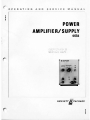
POWER
AMPLIFIER/SUPPLY
467A
I
f
PLUSc i'�URr, TO
sm','Ic::. DEPT,
ij
HEWLETT
r
PACKARD
Scans by ArtekMedia © 2008
.----- HEWLETT
CERTIFICATION
The Hewlett-Packard Company certifies that thi:; instrument was
thoroughly tested and inspected and found to meet its publi:;hed
specifications when it was shipped from the factory. The Hewlett
Packard Company further certifies that its calibration measure
ments are traceable to the U.S. National Bureau of Standards to
the extent allowed by the Bureau's calibration facility.
WARRANTY AND ASSISTANCE
All Hewlett-Packard products are warranted against defects in
materials and workmanship. This warranty applies for one year
from the date of delivery, or, in the case of certain major compo
nents listed in the operating manual, for the specified period. We
will repair or replace products which prove to be defective during
the warranty period provided they are returned t o Hewlett
Packard. No other warranty is expressed or implied. We are not
liable for consequential damages.
Service contracts or customer assistance agreements are available
for Hewlett-Packard products that require maintenance and re
pair on-site.
For any assistance, contact your nearest Hewlett-Packard Sales and
Service Office. Addresses are provided at the back of this manual.
OPERATING AND
(HP PART
NO.
SERVICE
00467-90003)
MODEL
POWER
MANUAL
467A
AMPLIFIER/SUPPLY
SERIALS
PREFIXED:
44-4-
Copyright Hewlett-Packarei Company 1965
P.O. Box 301, Loveland, Colorado, 80537 U.S.A.
Printed AUG 1969
Scans by ArtekMedia © 2008
Scans by ArtekMedia © 2008
Model 467A
Table of Contents
List of Tables and Illustrations
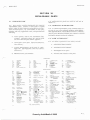
TABLE OF CONTENTS
Section
I
GENERAL INFORMATION
1-1. Description
1-3. Output Capability
1-5. Power Supply
1-7. Instrument Identification
Page
I-I
Section
11
INSTALLATION
2-1. Inspection
Page
2-1
2-1
2- 1
2-1
2-3.
2-5.
2-7.
2-9.
I-I
Section
V
MAINTENANCE
. . ..... .
5-1. Introduction
5-3. Test Equipnlent Required
5-5. Performance Checks
5-7.
Power Amplifier Opel·ations
IX: Power Supply Operation
5-12.
1-1
1-1
1 -1
. . . . .
Installation . . ...
Power Requirements
Three-Conductor Power Cable
Repackaging for Shipment
5-16.
5-\7.
5-18.
Ripple and Noise Check
Current Limit Check ....
5-19.
Power Supply Voltage Checks
5-20.
5-21.Adjustment and Calibration
2-1
2-\
5-23.
5-24.
5-27.
Page
3-1
3-1
3-1
3 -3. Description oC Controls
3-\
3 -S. Operating Instructions .
3-7.
Amplifier Operating Instruction!!
3-1
Power Supply Operating Instruction s 3-1
3-8.
Section
III OPERATING INSTRUCTIONS
3-1. General
........
Section
IV
THEORY OF OPERATION
4 -1. Introduction
4 -S. Block Diagram Description
4-9. Schematic Diagram Descriptlon
4-11.
4-13.
4-15.
4-17.
IlIgh Frequency Amplifier
Low Frequency Amplifier
Differential AmpllIier
Voltage Amplifier
4-19.
Driver Ampli!ier ...
4-21.
Output Circuits ... .
4-23.
External Load Protection
4-25. Power Supply Circuli Description
Minus 34 Voll Supply
4-27.
Plus 34 Volt SuPIJly
4-29.
Reference Supply ..
4-31.
Page
4-1
4-1
Output Impedrulce Check
Capaciti\'e Load Check ...
5-28.
5-29.
. .. . . . . .
Procedures
Zero Adjust
... . .. .
Current Limit Adjustment
IX: Gain Adjustment (R147)
Balance Adjust (CI24)
High Frequency Compensation
Acljustmcnt{C301, C303, C305)
AC Gain AdjlJstment (R14B)
5-31. Troubleshouting TechniqlJes
5-38.
Servicing Etched ClrclJll Boards
5-30.
Section
VI REPLACEABLE PA R T S
4-l
4-l
4-1
4-1
5-1
5-1
5-1
5-1
5-1
5-4
5-4
5-4
5-5
5-5
5-5
5-6
5-6
5-6
5-6
5-6
5-7
5-7
5-7
5-7
Pa!,;:e
6-1
6-1. IntrodlJction
6-1
6-4.
6-'
Ordering InformatIOn
4-l
4-2
4-2
4-2
4-2
Appendix
4-2
4-2
A
CODE LIST OF MANUFACTUR E R S
B
SALES AND SERVICE OFFICES
4-2
4-2
Page
6-6. Non-Listed P:u'ts
6-1
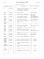
LIST Of TABLES
Page
Number
I-I. Specifications . . ... . . .
5-1. Test EqlJipment Required
5-2.
5-3.
5-4.
1-0
5- 0
5-2
5-3
5-4
AC Calibl·ation and Gain Check
Parts Cor Figure 5-SB.
IX: Power Supply Operation
Number
P;l/-:('
5-5. Power Supply Voltage Checks ... ..
5-5
5-6. Troubleshooting-Front Panel Symptoms
5-11
5-7. Power SlJppIy Checks
S-9
6-1.
Replaceable Paris
6-2
LIST OF ILLUSTRATIONS
Number
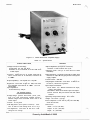
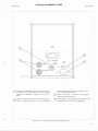
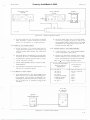
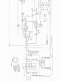
I-I. Model 467A Power Amplifier/Supply
3-1. FroI'! Panel Controls, Indicators and
Connectors
........... .
3-2. Rear Panel Controls ancl Connectors
4-1.
Simplified Block Diagram
5-1. AC Accuracy and Gain Check
5-2. Output Capability Check
5-3A.Distortion Check
5-3B. I MHz Rejection Filter .
5-4.
Output Impedancc Check
Page
1-0
3-2
3-3
4-0
5-1
5-2
5-3
5-3
5-5
Number
5-5. CUrrent Limit Check
5-6.
5-7.
5-8.
5-9.
5-10.
5-11.
. . . . . . . . . .
Pag-�
5-5
Balance AdjlJst . .
. 5-6
High Frequency Compensatlun AcljlJstmenl
5-7
Troubleshoolinl:: Tree
. 5-9
. 5-10
Top View . .
Side View .. .....
Rear Panel . . . .. .
. 5-10
.5-10
5-12. Printed Circuit Board (Al), PariS
Location
.5-11/5-12
. . .... .
5-13.Schematic. Power Amplifier
. 5-11/5-12
5-14.Schematic, Puwer Supply
. 5-13/5-14
.
ili
Model 467A
Section I
,b
_·• ......
.-...... .
. .. ,UT
'q9 *'"
•
�Aft. aAlN
VOLTS AOJ.
LINE
"
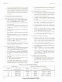
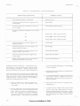
Figure 1-1. Model 467A Power AmplUier /Supply
Table 1-1.
Specifications
GENERAL
POWER AMPLIFIER
Voltage Gain (non-inverting):
Fixed steps: XI, X2, X5, XID.
Variable: 0-10, resolution is better than 0.1%
of full output.
Output Impedance (front panel connector):
Nominal: 5 mn in series with IIJ. H.
Accuracy: :i0.3% from dc to 10 kHz with load of
>40 n; :i1. dit from dc to 100 kHz; :ildit from dc
to 1 MHz.
Ripple and Noise: Less than 5 mV peak -to-peak when
referred to output for all gain positions and power
supply outputs.
Output Capability: ± 20 V peak at 0.5 A peak.
Distortion: Less than 0.01% at 1 kHz; less than
1% at 100 kHz; less than 3% at 1 MHz. For full
rated output.
Input Impedance:
50 kn shunted by 100 pF.
OC POWER SUPPLY
Voltage Range: greater than:!: 20 V, ±10 V, :i4 V,
:i2 V., :it V, with continuously variable vernier
between ranges with resolution better than O. 1%
of full output.
Current: :i0. 5 A peak.
Load Regulation (front panel connector): Less
than 10 mV for load change from 0 to 0.5 A.
Line Regulation: Less than 10 mV for a ±Idit
change in line voltage.
Capacitive Load:
instability.
Current Limit:
0.01 IJ.F or less does not cause
<800 mA.
Temperature Coefficient: Less than
±2 m V,fOC, whichever is greater.
O.Os%,fOc or
Input-Output Terminals:
Front Panel: 3/4'· Banana termInals for Input,
output, and chassis.
Rear Panel: BNC terminalsfor input and output.
Circuit Ground: May be floated 200 Vdc above
chassis.
Operating Temperature Range:
Weight:
OOto +500C.
Net 10 lbs. (4,5 kg).
Power Required: 115 or 230 V
<35 W at full load.
Dimensions:
Width: 5-1/8" (130 mm).
Height: 6-1/2" (165 mm).
Depth:
11" (279 mm).
1-0
Scans by ArtekMedia © 2008
:ildit, 50 to 400 Hz;
Model 467A
Scans by ArtekMedia © 2008
Section I
SECTION
GENERAL
INFORMATION
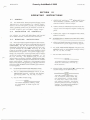
1-1. DESCRlPTlON.
1-2. The solid state 467A Power Amplifier/Supply
is a 10 "'"att peak power amplifier and -20 to ...20 volt
de power supply. The powel· amplifier has a wide
bandwidth with low de driLt frolll de to 1 MHz offering
wide applications wherever a power source is re
quired. Low distorlion « 0.01%), low drift and 0.3%
gain accuracy are obtained with high quality compo
nents and multiple teedback techniques. The gain of
the amplifier may be varicd between one and ten by
a front panel switch which provides Cixed gain steps
accurate to ±o. 3%. A variable gain control enables
the user to set the gain anywhere between zero and
ten with a resolution of better than 0.1% of fun output.
Table 1-1 g1ves the specUlcanons for the 467A Power
Amplifier/SUpply.
1-3. OUTPUT CAPABILITY.
t -4. An output greater than
20 volts peak and O. 5
ampere peak is available from de up to I MHz. The
amplifier is protected at ail times from short cir
cuits. The input Circuit of the 467A Is protected
against damage from voltages up to 200 volts Pop.
Input and output connectors are pI'ovided at the front
and rear of the instrument. The amplifier is a three
terminal dcvice isolated from chassis and may be
floated up to 200 volts dc above chassis ground.
1-5. POWER SUPPLY.
1-0. A front panel switch converts the amplifier t o
power supply that delivers±20 volts de at cunents
up to ±O. 5 ampere. The output level is controlled
by a potentiometer which permits voltages 10 be set
with resolution of 0.1% of full scale. Full scale
ranges of±1, ± 2,±4, ± 10, and ± 20 volts are selected
by the trOnt panel range swilch.
3.
1-7. INSTRUMENT IDENTIFICATION.
1-8. Hewlelt-Packarduses a two-sectiOn eight-digit
serial number (000-00000). If the fil'st three dig-its
of the serial number on your instrument do not agree
with those on the title page of this r.lanual, change
sheets supplied with the manual will define differences
between your instrument and the Model 467A described
in this manual.
1-1
Model 467A
Section Il
SECTION
11
INSTALLATION
2-1.
INSPECTION.
2-2. Upon receipt, unpack and inspect the Instrument
for mechanical and electrical damage. Mechanical
inspection Includes visually checking the Instrument
for scratched and warped surfaces, damaged control
knobs, switches, and indicators, and signs of weather
exposure. The electrical inspection Involves checking
instrument operation against specification values given
in Table 1-1.
ReCer to Paragraph 5-5.
-------
NOTE
-------
REPACKAGING
2-9.
IT the instrument Is to be shipped
to HewleU-Packard for service
or repair. attach a tag to the in
strument identifyif\i the owner
and Indicating the service or repair
to be accomplished; Include the
model number and full serial
number of the instrument. In
any correspondence, identify the
instrwnent by model number,
serial nwnber, and serial number
prefix.
cabinet mounting. The instrument should be installed
where ambient temperature does not exceed 500C
(,,2"F).
REOUIREMENTS.
2-6. The Model 467A can be operated from a 115 or
23Qac volt±l�source at 50 to 400 Bz. Power CQR
nections are made by plugging the power cable (sup
plied with the instrument) into the AC POWER male
connector at the rear of the unit and the appropriate
An 0.8 ampere slow-blow fuse
power receptacle.
Is used for 115 and 230 volt operation.
2-11. IT original container is to be used, proceed as
Collows:
a.
E�:�i!��)
Ensure that container Is well sealed with
strong tape or metal bands.
2-12. IT or1iinal container Is 1I0t to be used. proceed
as follows:
BEFORE PLUGGING POWER
CABLEDlTO THE RECEPTACLE,
DETERMINE THAT THE LINE
VOLTAGE SWITCH ON THE REAR
PANEL IS SET PROPERLY TO
ACCEPT THAT VOLTAGE (115
OR 230).
POWER
Place instrumenlln orlginal container ifavail
able. If original container is not available,
one canbe purchased from your nearest -hp
Sales and Service Office.
b.
THREE·CONDUCTOR
SHIPMENT.
------- NOTE -------
2-4. The Model 467A Is a submodular unit that can
b e mounted on a bench, or in a rack or cabinet. It is
shipped with plastic feet and tilt stand in place. ready
for bench use. When used as a single submodule, i t
Is utIlized a s a bench unit only. When used In com
bination with other su bmo dule .unlts, a rack adapter
frame or combining case is available lor -rack or
2-7.
FOR
fer to Paragraph 2-11 if the original container Is to
be usedj 2-12 if it Is not. IT you have any questions,
contact your local-hp- Sales and Service Office. (See
Appendix B for office locations. )
INSTALLATION.
POWER
------
2-10. The following paragraphs contain a general guide
for repackaging of the Instrument for shipment. Re
ranty page in the front of this
manual.
2-S.
NOTE
When operating from a two-con
tact outlet, the grounding feature
can be maintained by using a three
pronged adapter and connecting
the green pigtail on the adapter
to ground.
-------
In ease of mechanical damage,
file a claim with the carrier im
mediately. If an electrical mal
Cunctionoccurs, refer to the war
2-3.
Manufacturer's Assoc1a.tion (NEMA) for rack and
cabinet grounding. The offset pin on the cable is the
ground connector.
CABLE.
2-8. All Hewlett-Packard instruments are equipped
with a three-conductor power cable, which complies
with the recommendations of the National Electrical
a.
Wrap instrwnent in heavy paper or plastic
before placing in an Inner container.
b.
Place packing material around all sides of
Instrument and protect panel face with card
board strips.
c.
Place instrument and inner container in a
heavy carton or wooden box and seal with
strong tape or metal bands.
d.
Mark shipping container with "DELICATE
rnSTRUMENT," "FRAGILE"
Scans by ArtekMedia © 2008
etc.
2-1
Scans by ArtekMedia © 2008
Model 467A
SECTION
OPERATING
3-1.
3-2.
GENERAl.
3-3.
DESCRIPTION
OF
INSTRUCTIONS
c.
Connect DC Voltmeter (-hp- Mode1412A) to the
467A OUTPUT terminals: adjust the ZERO
control to obtain a zero dc output.
d.
Connect the 467 A OUTPUT terminals to the de
vice to which the amplified signal Is being ap
plied.
e.
Connect the signal to be amplified to the 467A
INPUT terminals.
3-8.
POWERSUPPLY OPERATING INSTRUCTIONS.
CONTROLS.
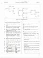
3-4. Figure 3-1 gives the description and function
of the 467A controls. indicators and connectors.
3-S.
III
The Model 467A Power Amplifier/ Supply can be
operated as a power amplifier or a power supply.
Controls on the front panel Jlrovide: (1) selection of
either operating mode and (2) selection of fixed or
variable amplifier gain and power supply ranges.
OPERATING
INSTRUCTIONS.
3-6. When operated as a power amplifier (non-invert
ing), the Model 467A has four calibrated gain factors
(AMPLIFIER: Xl. X2, X5, and XIO) and provides a
maximum output power of IOwatts peak for input fre
quencies between dc and 1 MHt. Accuracy of %0.3%
from dc to 10 kHz is obtained when operating Into a
load of 40 ohms or greater. As a power supply (regu
lated), the Instrument can be operated in five ranges
of plus or minus output voltages (SUPPLY: ±-1. %2,
:1:4, :1:10, and :1:20). The amplifier gain, or the :I: dc
output canbe varied with theVAR. GAlN/VOLTS ADJ.
control. The input and output terminals are dc isolated
a.
Connect the467A OUTPUTtermina!s to the de
vicctowhich the power supply Is being applied.
b.
Set 467A AMPLIFIER/SUPPLY control in the
SUPPLY range to the desired voltage settinl<
(:1::1, :1:2, t4, :1:10, or :1:20).
c.
a.
AMFLIFIER OPERATING INSTRUCTIONS.
Set the AMPLIFIER/SUPPLY control to the
AMPLIFIER poSition, selecting the desired
gain setting (VAR . Xl, X2, X5, or XIO).
.
b.
Set the LINE switch to 0:'11 .
NOTE
-----
To assure maximum stability. allow
the Instrument to warm up for 30
minutes.
Set the LINE Switch to ON.
-------
from earth ground. Connection of a grounding strap
between the power line ground (""") and (d,) terminals
references both the INPUT and OUTPUT (mt terminals
to earth ground.
3-7.
Section m
NOTE
------
To assure ma.xilllulll stabilizalior:,
allow the instrument to warm up
for 30 minutes.
d.
Using theVAR. GAIN VOLTS ADJ. control, ad
just the voltage to the desired level.
------ NOTE
TheVAR.
------
GAIN VOLTS ADJ. con
trol is used for both coarse and
fine adjustments. Coarse adjust
is made after either limit of the
fine adjust Is reaChed. Full CCW
position produces maximum negaU ve
voltage. Full CW position produces
maximJrn positive voltage.
3-1
Model 467A
Section m
2
467A POWER AMPLIFIER
I1[WLETT
PACK""O
3
/-j::t;;:,
VAA. GAIN AMPLIfiER SUPPLY
VOLTS AOJ.
VAR
!I
XIO
X5
o
LINE
ON
±2
±4
,
:t10
120
XI
,
•
INPUT
ZER
LINE ON: switches voltage on; Indicator
glows when ac line voltage Is ON.
o
AMPUFiER/SUPPLY: selects pow-er ampli
fier or power supply mode of operation Cor the
lru;trumunt.
AMPUFiER (Xl, X2, X5, XIO): selects the
fixed step gain factor.
OUTPUT
VAR.GAlN: operates in conjunction with AM
PUFiER (scJ.cctor in VAR. position) to pro
vide variable control oC amplifier gain any
where between zero and XIO.
VOLTS ADJ.: operlll.es In conjunction with
SUPPLY control position to provide variable
control of dc output voltage anywhere between
o volts and .:1:20 volts.
AMPUFtER (VAR.): operates in conjunction
with VAR.GAIN to provide variable control of
INPUT: banana-type connectors that provide
signailnput andcircult common Input connec
amplifier galn anywherebetwcen zero andXlO.
tions for the Instrument.
SUPPLY: selects rutl scale ranges of:l:l, .:1:2,
ZERO: a screwdriver adjust that provides com
pensation for dc oUset, or unbaiance, with no
signal applied to the 467A INPUT termln.1.Js.
.:1:4 . .:1:10. or .:1:20 volts.
o
O
VAR.GAIN/VOLTS ADJ.: operates In conjunc
tion with AMPUF1ER/SUPPLYcontrol to pro
vide variable control oCampUller gain or selec
tion of :t. de output voltage.
Figure 3-1.
OUTPUT: banana-type connectors that provide
signal output.clrcult common.a.nd chassis output
connections for the Instrument.
Front p:lne l Control$, Indicators and Connectors
3- 2
Scans by ArtekMedia © 2008
Scans by ArtekMedia © 2008
Model 467A
Section ill
2
•
161A-8-0091
�
�
INPUT
@ 115/230V
,,-_O.BA
OUTPUT
INPUT and OUTPUT connectors; these BNC
connectors are connected in parallel with the
INPUT and OUTPUT terminals on the front
panel.
FUSE: contaIns a fuse which provides protec
tion for the primary circuit of the instrument
Figure 3-2.
o
o
power translormer. This fuse is used for both
115 v and 230 v operation.
CD
CD
Power Connector: accepts a 3-wlre power
cable with saIety ground.
Line Voltage: a two-position slide switch; sets
the 467A for 115 or 230 volt operation.
Rear Pa."Iel Controls and Connectors
3-3
Model 461A
Section IV
�
<>.
"
•
!'."
L-�--'':
�
;
•
•
,
,
'"
,
,
•
"
·
•
•
·
·
L
--r -'I
__
,
•
;
•
__
•
•
i
,
,
4-0
•
.
"
"
"
,;: �3
Scans by ArtekMedia © 2008
w
.'"
-"
.
Scans by ArtekMedia © 2008
Mode! 467A
SECTION
THEORY
-4.1.
OF
4-2.
The Model 467A Amplifier circuits include a
high frequency amplifier, a low Crequency amplifier.
atwo-stage<iifierenlia! amplifier. a driver amplifier,
and two power amplifier stages. These circuits pro
vide two modes of operation, the J)()\\'er amplifier
mode and the IlOwer supply mode.
4-3. When the AMPLIFIER/SUPPLY switch is in the
AMPLIFIER position. the gain can be set in fixed steps
of Xl, X2, X5 and XlO. When the switch is In the
AMPLIFIER/VAR position, the VAR GAIN/VOLTS
A.DJ control can be used to set the amplifier gain to
any value between zero and ten. The input signal I s
applied to the attenuator, which selects the gain to b e
used by the instrument amplifier Circuitry. Ac and
dc feedback stabilize the amplifier gain. Compensation
for dc oUset, or unbalance, is provided by a ZERO
adjust control on the front paneL
4-4. When the AMPLIFIER/SUPPLY switch is In the
SUPPLY position, the amplifier provides five power
supply voltage ranges: -:1:1. ±2, -:1:4. -:1:10 and ±20 volts,
variable from plus through zero to minus for each
range.
An internal dc reference vollnge (plus or
minus) is applied to the amplifier portion, which pro
Vides a regulateddc voltage at the OUTPUT terminals
of the instrument.
4-S.
4-6.
467A.
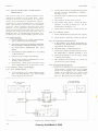
BLOCK
DIAGRAM
IV
OPERATION
4-9.
INTRODUCTION.
DESCRIPTION.
Figure 4-1 shows the block diagram for the
The Input signal is applied to the high and low
frequency ampliliers. The high frequency amplifier
(QlOl) amplifies the ac signal; the low frequency am
plifier (Ql08 through QII0) amplifies the dc and low
frequency signals. The ampllIied input signal is then
applied through the dUferential amplifier (QI02 and
Ql03), amplifier (QI04). and driver ampliller (Ql05)
to emitter followers (Ql06 and QI07). Power ampli
fiers Ql andQ2 (driven by Ql06) and Q3 and Q4 (driven
by Ql07) provide a b..1.lanced signal to the OUTPUT
connectors.
4-7. At frequencies above 1 MHz, negative feedback
from the driver amplifier QI05 Is applied to QIOl
through C122 and R129 to provide a decrease in dis
tortion and remove the power amplifiers from the
feedback loop. Negative feedback from QI05 Is applied
to dlfferentlalampllflers QI02 and QI03 through R120.
C 1 1 5 and R119 to improve frequency response of the
Instrument. Gain control for high frequency ampUfier
Q 1 0 1 Is supplied from the output of the power amplifiers
(QI through Q4) through R148 and R130.
4-8. At frequencies between dc and 50 KRz, negative
feedback Crom the output provides dc gain control and
balance adjust for the low frequency amplifiers QI08
through QIlO. ZEROadjust R 5 p rovldescompensatlon
for dc unbalance of the signal applied to the low Cre
quency amplifiers. Relay KI protects the eltterna l load
against current surges during turn-on and turn-off.
Section IV
SCHEMAIIC
DIAGRAM
DECRIPTlON.
4-10. The following paragraphs give a detailed descrip
tion of the �1odel 467A Amplllier circuits. Refer to
Figures 5-13 and 5-14, Section V, for the schematic
diagrams of the Instrument.
4-11. HIGH FREQUENCY AMPLIFIER.
4-12. Trimmer capacitors C301, C303 and C305 can
be adjusted to provtde the desired frequency response
characteristics for the instrument. Ac input signals
from the attenuator are applied through CIO! to the
high frequency amplifier Ql01. The signal Is amplified
by QIOI and coupled through CI04 to the base circuit
of QI02. The RC networks, CI05, R112. Cl06 and
R1l4 are used to Improve the frequency response
characteristics orthe amplifier QI02. The bias volt
age of QI01 Is determined by resistive divider RI03
and R104. Ac feedback from power amplifiers (Ql,
Q2, Q3, and Q4) is applied through R148 to provide
ac gain adjust for QIOI.
4-13. LOW FREQUENCY AMPLIFIER.
4-14. When the AMPLIFIER/SUPPLY selector Is in
the SUPPLY poSition, +7 and -7 volts are suppUed
from an Internal reference. through resistive diViders,
to the ampliCier Input. Each SUPPLY position (-:1:1,
:1:.2, :1:.4, :1:.10 and :1:.20) permits setting the dc output
voltage to any ± value within the range selected. The low
frequency amplifier circuit (Ql08. Ql09 and QUO) am
plifies the dc and low frequency input signal and drives
Ql03. The bias voltage fol' the low frequency amplifier
is controlled by R132 and R133 and the ZERO control
R5. TranSistor Ql10 is a current source for the dif
ferential amplifiers QI08 and QI09. Inductors LIOI
and Ll02 control the frequency response of the low
frequency amplifier (at higher frequencies) by causing
degeneration of QI08 and QI09 emitters. High fre
quencies present at QI09 collector are shorted to
ground by CI09.
Low frequency stabilization and over·
all amplifier gain (between dc and 50 KHz) are provided
by applying dc feedback from the OUTPUT to QI09
base. The ZERO potentlometer R5 provides an adjust
ment to compensate for dc drift in the instrument.
VaryingR5 changes the voltage at QI09 base. thereby
changing the output level of the low frequency ampli
fier.
4-15. DIFFERENTIAL AMPLIFIER.
4+16. Differential ampllCiers QI02 and QI03 provide
an output proportional to the input signals from the
high frequency amplifier QIOl and the low frequency
amplifier circuit (Ql09 and QIlO).
The high fre
Quency nc signals are coupled to QI02 through CI04;
the dc and low frequency signals Crom the low fre
quency amplifier are direct-coupled to differential
amplifier QI03. capacitor CI08 bypasses any high
frequency ac from the low frequency amplifier to
4-1
Mcdel 46'7A
Section IV
ground. CI09 bypasses any high frequency signals
present at the Case of QI03. Ac feedback from QI05
collector circuit ill applied through ellS to the balle
circuit of QI02 for high frequency gain stabillzation.
4-17. VOLTAGE AMPLIFIER.
4-IB. The voltageampUfierQI04 supplies the majority
of the voltage gain for the Instrument.
Degeneration
at low frequencies Is provided by R12'7 In the QI04
emitter circultj CI16 provides added phase stability
at high frequencies. Current through R125 provides
the bias current for QI05. Breakdown diode CRI04
establishes the proper voltage at QI04 collector and
maintains a dc signal path from QI04 Collector to
QI05 base.
4-19. DRIVER AMPLIFIER.
4-20. Driver amplHierQI051s driven by current am
plifier QI04 and supplies the signai to the power out
put ampliHers. Transistors QI06 and QI07 are for
ward biased bydiodesCRIOB through CR112and under
no-signal condition are conducting slightly to reduce
cross-over dlst::lrtion In the output signal.
4-21. OUTPUT cmculTs.
4-22. Transistors QI through Q4 provide a comple
mentary symmetry output. QI and Q2, driven by
emitter followerQI06, provide a low output impedance.
Q3 an<! Q4, driven by QI07, form a unity gain feed
back amplifier. ThlscausesQ3and Q4 t o a c t a s a PNP
emitter follower, which is necessary to provide the
complementary symmetry output.
4-25.
4-24. The external load connected to the 46'7A is pro
tected during turn-on and turn-off. from current surges
and voltage transients. by relay KI. The relay con
tacts open the circuli totheO UTPUT connectors when
the relay Is de-energized. When the instrument is
turned ON, Kt remaln� de-energized lor about 300
milliseconds. This delay permits the instrument to
stabilize before the output Is connected to the load.
The 300 millisecond delay Is caused by the RC time
constant of CIIO and RI6I.
When the Instrument Is
turned off. the relay quickly de�energlzes and opens
the circuit to the OUTPUT connector.
SUPPLY
CIRCUIT
-1-26. The 467A prlmary power !;1,Jpply cUIl:sllit:s ullwo
regulated power supplies ,"34 and +34 volts), and five
reference supplies (+7. -7, +15. -15 and +30 volts).
Either 115 or 230 volts ac Is connected to the Instru
ment through switch SI and fuse Fl to Tl primary.
Switch S2 (slide switch on rear panel) con:lects Tt
primary wlndings in series for 230 volt operation, or
:n parallel lor 115 volt operation. The LINE ON lamp
OSl glows when primary power Is applied to the instru
ment.
4-27. MINUS 34 VOLT SUPPLY.
�-2B. Transistor QI12 In conJunCUon with R156,
CR129, and CR130 provide a constant current source
which provides base drive for Q5 and Q6. Q1l2 also
provides current to keep CR131, CR132, CRI33, and
CRI35 conducting. R2 and Q5 share the load current
to reduce the dissipation In Q6. F o r small load
currents Q5 Is turned off and resistor R2 supplies the
current. As the load current Increases,the base of
Q5 Is forward biased and Q5 conducts, sharing the
current. As the load current Is Increased further,
CR1341s forward biased at a current level determined
by R159. This will reduce the current in CRI35 to
zero causing the supply voltage to go to zero also.
4-29.
PLUS 34 VOLT SUPPLY.
4-30. The +34 volt supply provides regulated voltage
to the power ampllller circuits. Breakdown diode
CRI43 establishes the reference at the base of Q8.
P otentlometer RI63 adjusts the current limit setting
:or the +34 volt supply.
�-3t.
4-23. EXTERNAL L O A D PROTECTION.
POWER
DESCRIPTION.
REFERENCE SUPPLY.
4-32. The diode regulated reference supply (refer to
Figure5_14)provides .7. -7. +15 and -15 voltages.
Capacitors C126 and C l 2 8 filter the ac voitages.
Breakdown diodes CR146 and CR14'7 maintain a +15
reference voltage at the junction of R149 and R lSO.
The series arrangem!lnt of diodes CR120 and CR121
(forward biased diodes) and CRI22 and CR123 (re
co mpe neat e e lor temperature
and provides a constant -15 reference voltage at the
junction of R151and R152. The plus and minus '7 volt
reference voltages are obtained In the same manner
as the plus and minus 15 reference voltages. Series
regulator QllI provIdes regulated +30 volts to the
positive side of the reference supply.
veTl!e blaeed diodee)
'-2
Scans by ArtekMedia © 2008
Scans by ArtekMedia © 2008
Section V
Table 5-1.
Instrument
Model 467A
Test Equipment Required
CritlcalSpecUicattons
U"
Recommended Model
Performance Checks
Calibration
-hp- Model 3440A 3444A
Digital Voltmeler
DC Voltmeter
Accuracy: ± D. 05
Range: 1000 mV to 100 V
OscHlator
Frequency: 10 Hz to 1 MHz
Output: l.O V
tput I m e
50 or 600 ohms
���r:
Performance Checks
Calibration
-hp- Model 651B Test
Oscillator
AC Voltmeter
Frequency: 10 llz to 100KHz
Range: 10 V
Accuracy: ±0.1 to:l:O,3":'
Performance Checks
CalH)l'atloll
-hp- Model 3440A/3445A
Digital Voltmeter
AC Voltmeter
Frequency: lOO KHz to I MHz
Range: 0.001 tCl 30 V
Accuracy: :l:S%
Perlormance Checks
Calibration
-hp- Model 33lA DlslorUon Analyzer
Variable Line
Transformer
Output:
Distortion
Analyzer
Frequency: 100 KHz
Range: 0.01% 10100%
O�
�
103.5 V to 127.5 V
Perlormance Checks
Superior Electric Model
UCIM
Perlormance Checks
-hp- Model 33IA Distorlion Analyzer
Accuracy: :!: 3%
DC Standard
Outpul: I.OV
Accuracy: O. 05':
Performance Checks
Calibration
-hp- Model 741B DC
Slandard
Range: 1000 mA
Accuracy; ± 3':(,
Perlormance Checks
Calibration
-hp- Model 428B D C
MUHamnleter
Oscilloscope
Frequency:
Performance Checks
-hp- Model 140A(l402(
420A
Capacitor
0.01 j1.F:l:lCfl. 200 V
Performance Checks
-hp- Part No. 0160-0304
Resistor
40 ohms :1:5% 10 watts
Performance Checks
-hp- Pari No. 081S-0028
2 ohms:l: 1% 1/2 watl
Performance Checks
-hp- Part No. 0727-0445
12 ohms:!:t% 1/2 watt
Performance Checks
-hp- Part No. 0811-0297
PerCOrmance Checks
-hp- Part No. 0727-0081
DC Mllllammeter (cl ip
on)
to IS MHl.
600 ohms:I: 1% 1/2 watt
Calibration
Filter
Bandpass: 1 KlI'
Bandwidth: 50%
Distortion Check
White Instrument Lab.
264S-1K
Filter
Bandpass: 100 KHz
Bandwidth: 50%
Distortion Check
White Instrument Lab.
5-0
264S-10OK
Scans by ArtekMedia © 2008
Scans by ArtekMedia © 2008
Model 467A
SECTION
Section V
V
MAINTENANCE
c. Connect the DC Standard outpJt to the Model
467A INPUT. Adjust the voltage output of
the DC standard to 1. 000 V on the dc volt
meter. The output of the 467A should be
10.00 V :1:0.3%. If not, refer to Para
5-1. INTRODUCTION.
5-2.
This section contains Information necessary for
the proper maintenance of the -hp- Model 467A Power
Amplifier/SUpply. This section provides the necessary
Performance Checks, Adjustment and Calibration
Procedures, and Troubleshooting Techniques re
graph 5-27 for proper adjustment.
d.
Set the 467A to AMPLIFIER X5. The 467A
output should be 5.000 V ±Cl. 3%.
5-3. TEST EOUIPMENT REQUIRED.
e.
Set the 467A to AMPLIFIER X2. The 467A
output should be 2.000 V ±Cl. 3%.
5-4. The test equipment required to perform the
operations outlined in this section Is lIsted In Table 5-1.
t.
Set the 467A to AMPLIFIER Xl.
output should be 1. OOOV :to. 3%.
g.
Set the 467A to VAR.; rotate the VAR.GAIN
from fully CCW to fully CW. The 467A out
put should vary !l'om 0 V to 10 v.
quired to accomplish the above objective.
This table describes the type of instrument required,
critical specifications, type of operation to be con
ducted, and the reenmmenrlerl model. Tf the spectfic
model recommended is not available, equipment whIch
5-9.
meets or exceeds the critical specifications Hsted
may be substituted.
AC ACCURACY AND GAIN CHECK.
a.
5-5. PERFORMANCE CHECKS.
5-6. The performance checks presented In thIs sec
tion are front panel procedures designed to compare
the Model 467A with Hs publiShed specifications.
POWER AMPLIFIER OPERATIONS.
5-8.
DC GAIN CHECK.
a.
A DC Voltmeter (-hp- Model 3440A/3444A)
and a DC standard (-hp- Model 741B) are
required for this test.
b.
Set the Model 467A to AMPLIFIER XIO.
hp 651B
II.@
.. "
. . _..
]
El @<j>
o
b.
Connect the 600 ohm load resistor across
the 600 ohm OUTPUT of the oscillator.
Connect to the INPUT of the Model 467A.
Set 651B ATTENUATOR to IVand FREQUE
NCY to 100kHz.
c.
Connect the 3445A INPUT to the INPUT of
the 467A ( A in Figure 5-1). Advance the
AMPLITUDE of the Oscillator until the ac
voltmeier reads 1. OOOV.
d.
Using a 4 0 n load resistor. connect the 3445A
rnPUT to the OUTPUT of the 467A (B in
Figure 5-1).
Set 467A to AMPLIFIER XIO.
The ac voltmeter should read 10.00 volts
:1:1. 0%.
If the reading is not within toler
ance. see Paragraph 5-30 for adjustment.
hp 467A
TEST OSCILLATOR
@
Figure 5-1 shows the test set\lp recommend
ed. A Test Oscillator (-hp- Model 651B).an
AC Voltmeter (-hp- Model 331A and 3440A/
3445A). 40 and 600 ohm loads are required.
Use the 331A Voltmeter for the 1 MHr. fre
quency. Use a 3440A/3445A with known ac
curacy at 400 Hr. and 10 kHr..
These operations may be incorporated in periodic
maintenance, post-repair, or Incoming quaUty can
trol checks. These operations should be conducted
before any attempt is made to adjust or calibrate the
instrument. During these operations, the Model 467A
power line voltage should be periodically varied :1:10%.
A fifteen minute warm-up period should be allowed
prior to conducting these checks.
5-7.
@
tiC VOLTMETER
POWER AMPLIFIER
®
',1'''1\
I
Figure 5-1.
o@;;
"
The 467A
e
hp 3440A 13445A
f, - --I@
.db±'"1'
I
,
�I
•••
I
•
0
I�
I)
-
"
AC Accuracy and Gain Check
5-1
Section
Model 467A
V
b. Connect the Model 467 A as shown in Figure 5-2.
e. Repeat steps b through d Cor each of the os
cillator settings and Am plifier settings listed
In Table 5-2. For each measurement, con
nect the ac voltmeter first to the INPUT of
the 467A and adjust for 1. 000 V. Then con
nect the ac voltmeter to the OUTPUT of the
467A. The reading should be between the
Umits lIsted in the last column. IT not, see
adjustment procedures, Paragraphs 5·28
through 5-30. For 1 MHz output frequency,
use 331A AC Voltmeter.
Set ae voltmeter RANGE to
d.
Set Model
e.
Set test oscillator frequency to
justoseUialor output ampLHude
a.
A Test
OscUlator (-hp- Model 6518), an AC
Voltmeter (-hp- Model 331A) and 40 ohm
and 600 ohm load resistors will be required.
Table
Model
Frequency
Dial
R"",.
Figure
5-3A describes the test arrangement
recommended. A Distortion Analyzer (-hp
Model 331A), an Oscillator (-hp- Model 651B),
a 1 KHz Bandpass Filter (White Instrument
Model
for 3445A
Adjusted
Reading
of:
1. 000 V
3
467A
Model 3440A/3445A
AC Voltmeter Reading
Amplifier
(Output of 467A)
9.900 to 10.100 V
4.950 to 5.050 V
1 . 980 to 2.020 V
0.990 to 1.01 0 V
greater than 10 V
XlO
X5
X2
Xl
VAR-CW
3
XIO K
I
1.
000 V
9.970 to 10. 030 V
4.985 t o 5.015 V
1 . 994 t o 2.006 V
0.997 to 1. 003 V
greater than 10 V
Xl.
X5
X2
Xl
VAR-CW
XlOO
4
I.
3
Xl.
X5
000 V
9.970 to
4.985 to
1.994 to
0.997 to
10.030 V
5.015 V
2.006 V
1.003 V
greater than 10 V
X2
Xl
VAR-CW
Xl M
I
3
1. 000 V·
9.00
4.50
1. 80
0.90
Xl.
X5
to 11.00 V'
to 5.50 V'
to 2.20 V'
t o 1.10 V'
greater than 1 0 V
X2
Xl
VAR-CW
•
read on 331A Voltmeter
At 10 kHE and 400 HI,
NOTE:
KID.
AC Calibration and Gain Check
Amplifier
Output
Attenuator
467A to AMPLIFIER
400 Hz . Ad
to provide ae
voltmeter r eadin g oI 14. 14 V rms (20 V peak).
Current through 400hm r es is tor will then be
0.3535 amps (0.5 A peak).
651 BOscillator
XIOOK
I
5-2.
30.
5-11. DISTORTION CUECK.
5-10. OUTPUT CAPABILITY CHECK.
a.
e.
allow for possible error of 3445A of up to ±o. 1%.
TEST OSCILLATOR
hp651B
.@@O@
•
0
0
o.
hp 467A
POWER AMPLIFIER
�Ilf\
..,..�-,
Figure
5-2
uQ>.
•
AC VOLTMETER
hp 331A
/l�
n
�
5-2. Output Capabillty Check
Scans by ArtekMedia © 2008
� I�I
l '@ @
@�@
@
O .
o
•
Scans by ArtekMedia © 2008
Model 467A
FILTER SET
TEST OSCILLATOR
WHITE 2645-IK
hp 6518
.@@ E] @
ill
0
0
,,"'-0·_,.
@
hp467A
POWER AMPLIFIER
l
0
,
, -- ----- - - -- - -- - - ---,
e.
Description
0690-8231
0092-5125
2100-0006
0121-0021
0160-0439
0160-0474
9140 -0007
R: Cxd 82,000 n 1 W
R : [xd 5100 n 2 W
R: var 5000 n 2 w
C: var 5. S pF t0 64. 3 pF
C: fxd 22 pF
C: fxd 390 pF
Inductor : var 60-100 11 H
RI
R2
R3
Cl
C2, C3
C4, C5
L1
b.
d.
0 :
Rotate FUNCTION switch to DISTORTION.
Null out fundamental signal by alternately
reducing the meter range and adjusting
Connect the 1 KHz filter Input to the output of
the 651B, Test Oscillator , using a 600 ohm
load. Connect the 33tA Distortion Analyzer
directly tothe Filter output as shown in Fig
f.
Disconnect the filter output from the 331A.
Connect the filter output to the 467A input.
Connect the 467A output to the 331A input
across a40 ohm load, as shown in Figure 5-3A.
Set the 467A to XIO p05ition.
g.
Set the Distortion Analyzer FUNCTION to
SET LEVEL a n d adjust VERNIER for a Cull
scale reading of 1 (100%) .
h.
Rotate the FUNCTION switch to DISTORTION
and find the null again, The new reading
should add less than 0 . 0 1% (SO dB down).
1.
Repeat steps b through h using the 100 KHz
filler and 100 KHz frequency settings on the
651B and the 331A. Distortion added by the
467A at 100 KHz should be less than 1% (40
ure 5-3A Alternate connection.
c.
c;)
BALANCE and frequency centrol knob for a
null. Record the amount of distortion.
Parts for Figure 5-3B
-hp- Part No.
@�@
Distortion Check
Lab Mode12645 - 1 KHz) , a 100 KHz Bandpass
Filter (White Instrument LabMode12645-100
KHz) , 40 and 600 ohm load resistors , and the
resistors a n d capacitors listed in Table 5-3
will be reqUir ed for this test.
Designator
hp 331A
Ion' 0 @ ' 1l'�4, � I�@I
$oon�!�
� <O
Figure 5-3A.
Table 5-3
DISTORTION ANALYZER
R
WHITE 2645-100K
of
Section V
Set the osclllator frequencyto I KHz. Adjust
the output amplitude for the 1. 0 volt output.
dB down) .
j.
Set the Distortion Analyzer Frequency to 1
KHz; FUNCTION to SET LEVEL; SENSI
TIVITY to provide upscale dellection. Adjust
VERNIER for full scale reading of 1 (100%) .
For checkin g distortlon at 1 MHz, connect the
oscillator across a 600n load to the 467A nput.
i
Connect the 467A output aCrOS5 a 40 n load to
the Inputofa 1 MHzband reJection filte r , Fig-
r - - - - - - -- - - - - - - - - - - - - - - - - - ,
�
I
I
I
I
I
I
I
I
I
I
I
I
f- 00""'
�}
'''"' {�:
,
....·.·00'••
I
I
I
L
_ _ _ _ _ _ _ _ _ _ _ _ _ _ _ _ _
Figure 5-3B.
_ _ _ _ _ _
�
I
I
I
_
..J
1 MHz Rejection Filter
5-3
Model 467A
Section V
ure 5·38. Set the osciLlator Crequency to I MHz.
k.
Adjullt the ooelU:uor output for 10 V Ilt the 467A
output, using the ac voltmeter. Then connect
the ac voltmeter to the filter output and the
reading should be less than 0 . 3 V. The oscil
lator must have less than 1% distortion for
this check.
t.
tained in dabove. The load Is from 0 to O. 5 A.
5-15. LINE REGULATION CHECK.
a.
A DC Voltmeter (-hp- Model 3440A/S444A)
and a Variable Voltage Line TransfOl'rner
(Superior Electl"lc Company , Type UCIM) will
be required lor this operation.
b.
Connect the DC Voltmeter to the Model 467A
OUTPUT. Set FUNCTION to VOLTS; RANGE
to 10 V.
c.
Set Model 467A to SUPPLY ±10; VOLTS AnI
fully CCW. DC Voltmeter should read greater
than -10.00. Note and record reading.
d.
Connect variable voltage line transformer
between Model 467Apower plug and Unepower
source.
5-12. IX: POWER SUPPLY OPERATION.
5-13. DC VOLTAGE AND CURRENT CHECK.
a.
A DC Voltmeter ( -hp- Model 3440A/3444A)
and a 40 ohm :105%, 10 wait resislor (-hp
Part No. 0815-0028) will be required.
b.
Place the 40 ohm resistor across the Model
467A OUTPUT.
c.
Connect the dc voltmeter across the 40 ohm
resistor. Set FUNCTION 10 VOLTS; RANGE
to 1000 mV.
d.
Set Model 467A to SUPPLY ±1; VOLTS An)'
fully CCW.
e.
e.
DC Voltmeter should read greater th.an -1OUU
Rotate VOLTS ADJ fully cw. DC Voltmeter
should Increase from -1. 000 to + 1 . 000 V or
more.
g.
Repeat the above USing settings listed in
Table 5-4. Dc voltmeter sb>uld indicate
voltage variations as listed.
h.
In the final step , an output current of O. 5 A
will be verUled when the %20 V Is obtained
across the 40 ohm load resistor.
a.
A DC Voltmeter (-hp- Model 3440A/3444A) and
a 2 0hm %1%, l/2wattreslslor(-hp-Part No.
0727-0445) will be required for this operation.
b.
Connect DC Voltmeter to ModeI 467AOUTPUT.
Set voltmeter FUNCTION to VOLTS; RANGE
lo lO v.
c.
Set Model 467A to SUPPLY %1; VOLTS ADJ
fully CW.
d.
DC Voltmeter should read greater than +1. 000
V . Note and record reading.
e.
Turn Model 467A LINE to OFF. Connect 2
ohm load resistor across Model 467A OUTPUT.
Leave DC Voltmeter connected as In slep b.
a.
Figure 5-4 describes the test arrangement
recommended. AnAC VoUmeter(-hp- Model
33IA) , a Test Oscillator (-hp- Model 6518),
and a 12 ohm % 1%, 1/2 watt resistor (-hp
Part No. 0811 -()297) will be required.
b.
Connect the Model 467A as shown in Figure 5-4.
c.
Short Model 467A (root panel INPUT; set to
AMPLIFIER XIO.
d.
Adjust oscillator lor 1 . 0 V rms, 500 KHz
output. Verily output using AC Voltmeter.
e.
Voltage across 12 ohm resistor should be O. 8
V or greater. At SOO KHz, Model 467A
output impedance is 3 ohms or less where
E
E
E
ase .. 12 ohms + 467 ,
5-17. CAPACITIVE LOAD CHECK.
a.
Supply
I
2
•
10
20
CCW to CW
CW to CCW
CCW to CW
CW to CCW
CCW to cw
An OscUloscope (-hp- Model 175A) and 0 , 0 1
j.l F % IO%, 200 V capacitor (-hp- Part No.
0160-()304) will be required for this test.
b.
Set Model 467A to SUPPLY ±20; VOLTS ADJ
fully CW.
DC Power Supply Operation
Model 3440A/3444A DC Voltmeter
Model 467A
Volts AdJ
Rotate from Fully
Reset Une transfornler tor 103. � V output.
IX: Vollmeter reading should remain within
10 mV of reading obtained In c above.
5-16. OUTPUT IMPEDANCE CHECK.
5-14. LOAD REGULATION CHECK.
Table 5-4.
Adjust Une transformer for 126 . 5 V output.
DC Voltmeter reading should remain within
10 mV of reading obtained In c above.
f.
mY.
f.
Turn Modcl467A LINE ON. OC Voltmeter read
ing should remain within 10 mV 01 reading ob
R"",.
1000
10
10
10
100
mV
V
V
V
V
Funclion
VOLTS
VOLTS
VOLTS
VOLTS
VOLTS
Scans by ArtekMedia © 2008
Reading
(minimum desIgnated)
- 1 . 000
+ 2 . 000
- 4 . 000
+10.00
-20.00
to + 1 . 000
to - 2.000
to + 4 . 000
to -10.00
to +20.00
V
V
V
V
V
Scans by ArtekMedia © 2008
Model 467A
TEST OSCILLATOR
AC VOLTMETER
hp651B
hp
"@ @ E] @
..
0
0
Section V
"
· I�I
11c<ill
"-
0
hp 467A
331A
POWER AMPLIFIER
� �@
o@<
<ill 0° :
9
�
'"
;
,
.....,._,
Figure 5-4.
c.
Output Impedance Check
Connect capacitor and oscilloscope to Model
467A OUTPUT. Output waveform should be
stabLe (no oscillations or ringing present) .
b.
5-18. RIPPLE AND NOISE CHECK.
a.
An AC Voltmeter (-hp- Model 331A) will be
required Cor this operation. Connect AC Volt
meter to Model 467A output. Set RANGE to
0. 003 V.
b.
Set Model 467A to SUPPLY ± 2 0 ; VOLTS ADJ
fullyCW(-t-20 . 0 0 \I) . Short ModeI467AINPUT.
c.
AC Voltmeter should read less than 1 . 77 mV
rms (5 mV peak-Io-peak) .
d.
Rotate AMPLIFIER/SUPPLY switch to AM
PLIFIER XIO.
e.
AC Voltmeter should still read less than 1 . 7 7
mV rms ( 5 nlV peak-to-peak) .
Short the 467A output and connect the 428B,
set on the I A range, as shown in Figure 5-5.
As the VOLTS ADJ Is varied slowly, the 428B
should show an Increasing current that i s
always less than SOO mA.
5-20. POWER SUPPLY VOLTAGE CHECKS.
a.
A DC Voltmeter (-hp- Model 3440A/3444A)
will be required Cor this check.
b.
Connect DC Voltmeter between point desig
nated in Table 5 - 5 and circuitground. Volt
meter should display readings as indicated.
Table 5-5
Power Supply Voltage Checks
Connect IX:: Voltmeter
Between Circuit
Ground and
J2, Pin 7
5-19. CtmRENT LIMlT CHECK.
a.
A DC Milliammeter ( -hp- Model 428B) and a
OC Voltmeter (-hp- Model 3440A/3444A) will
be required. Set the 467A le SUPPLY ±20 ,
and adjust the VOLTS ADJ until an output volt
age of 0.000 volts is obtaineci, using the dc
J2, Ptn 2
J l , Pln 3
J I , Pin 4
Cathode of CR146
Anode of CRI23
+ Side of CllI
J2, Pin 1
DC Voltmeter
Readings
-32 . 5 to - 3 5 . 7 V
+ 3 2 . 2 to +36 o V
+ 7 V
- 7 V
+15 V
-15 V
+50 V
-50 V
voltmeter.
C L I P-ON
DC AMNETER
hp 4289
[I�II
hp 467A
POWER AMPLIFIER
oQ<
..... , OtoM
@
3�
Figure 5-5.
0
0
Current Limit Check
5-5
Model 467A
Section V
b.
S _ 21. ADJUSTMENT AN D CALIBRATION
c.
5-22. The following Is a complete adjustment and
calibration procedure for the Model 467A.
These
operations should be conducted only II it has pre
viously been established by Perforn:ance Checks,
Paragraph 5-5, that the Model 467A Is out of adjust
ment. Indiscriminate adjustment of the instrument
controls to "refine" readings may actuaUy cause more
difficulty. If the procedures outl ined below do not
rectUy any discrepancies that may eltist, and all con
nections and selllngs have been rechecked, refer to
A DC Voltmeter (-hp- Model 3440A/3444A)
will be required for this operation.
b.
Connect dc voltmeler to Mode1467A OUT PUT.
Set FUNCTION to VOLTS; RANGE to 100 mV.
Set Model 467A to AMPLIFIER XIO.
Short Model 467A output. Connect de mUll
ammeter as shown In Figure 5-5.
Set de
mUlJammeler RANGE to 1 A.
f.
Adj ust R159 for ammeter readlng of 650 mA.
Rotale VOLTS ADJ fuByCW (.. 20. O O V output).
b.
Adjust Rl63 for ammeter reading of 650 mA.
a.
A DC Standar d (-hp- Model 741B) and a DC
Voltmeter (-hp- Model 3440A/3444A) will be
required lor this operaUon.
b.
Set Model 467A to AMPLIFIER XIO.
c.
C onnect<ic vollmeter to Model 467A OUTPUT.
Set FUNCTION to VOLTS; RANGE lo 10 V.
on DC Voltmeter.
e.
Remove short at Model 467A INPUT.
C.
Adjust Rl3S (Internal adjustment) for zero
readlng on DC Voltmeter .
g.
I! necessary, repeat steps d through ( above
untU voltage difference Is less than 1. 0 mV.
d.
Adjust DC Standard for .. I V dc outp..Ll . Apply
to Model 467A INPUT.
e.
DC Voltmeter should read 10.0 V.
Just R147 for proper reading.
a.
(RI 59).
A DC Voltmeter (-hp- Model 3440A/3444A)
and a DC Milliammeter (-hp- Model 428B)
will be required for this test.
Figure 5-6 describes the test arrangement
recommended. A Test Oscillator (-hp- Model
651B), a OC VOltnleter (-hp- Model 3440A!
3444A), an AC Voltmeter (-hp- Model 33IA)
and a 40 ohm %5%, 10 watt resistor (-hp
Part No. 01315-0028) will be required.
OC VOLTMETER
TEST OSCILL.ATOR
hp
hp
651B
o@ @ EJ @
•
0
•
•
POWER AMPLIFIER
"'ff\
BNC-T1250·0072
o \) _
•
/l�g
AC VOLTMETER
hp
..'...._.
�
: I�I
�©
@-
331A
@ �@
�
o
O .
•
Figure 5-6. Balance Adjust
'-6
3440A 13444A
�I
hp 467A
AQAPTER
hp
U nol, ad
5-28. BALANCE ADJUST (C124).
5-24. CURRENT LlMlT ADJUSTMENT.
a.
e.
a.
Short
Adjust R5 (front panel ZERO) lor zero reading
5-25. -34 V ADJUST
DC Voltmeter should read -20.00 V.
5-27. DC GAIN ADJUSTMENT (R147).
INPUT.
d.
d.
5-26. . .34 V ADJUST (RI63).
5-23. ZERO ADJUST.
a.
Set Model 467A to SUPPLY %20; VOLTS AID
fully CCW.
Paragraph 5-31, Troubleshoollng Techniques, (or
possible cause and recommended corrective action.
c.
Connect DC Voltmeter toModel 467A OUTPUT.
Set DC Voltmeter FUNCTION to VOLTS;
RANGE to 100 V.
PROCE DURES.
Scans by ArtekMedia © 2008
r,
Id
•
-
I
©_©
0
Scans by ArtekMedia © 2008
Model 467A
b.
Connect Model. 467A as shown In Figure 5-6.
e.
c.
Sel OC Voltmeter FUNCTION
RANGE to 1000 mY.
Adjust R148 for a 10 volt reading on the AC
Voltmeter.
f.
Repeal ac accuracy and gain check, Para
graph 5-9. (AC Voltmeter readings should
to
VOLTS;
d.
Set Model 467A to AMPLIFIER XI O.
e.
AdjustosciUatorlor 1 . 4 V rms, 300 KHz out
put. (use AC Voltmeter to verify I. 4 V rms
signal level. )
f.
Tune CIM to minlmum dc output as read on
DC Voltmeter.
5-29. HIGH FREQUENCY COMPENSATION ADJUST
MENT (C301, C303, C305).
I
:l.
Figure 5-7 describeS the test arrangement
b.
Connect Model 467A as shown in Figure 5-7.
Set Model 467A to AMPLlflER XIO.
c.
Set the Test Oscillator (6518) u-equency to
1 MHz. Adj ust AMPLITUDE and OUTPUT
ATTENUATOR for AC Voltmeter reading o f
I . 0 V.
recommended. ATestOsclllator (-hp- Model
6516), 600 and 40 ohm loads and an AC Volt
meler (-hp- Model 331A) will be required.
d. Set Model 467A to AMPLIFIER X5. Tune
C305 for an A C Voltmeter reading between
0.498 and 0.502.
e.
Set Model 467A to AMPLIFIER X2.
Tune
5-30. AC GAIN ADJUSTMENT (R148J.
TestOsclllator (-hp- Model 6516), AC Volt
meters (-hp- 331A aoo 3440A/3445A), and 40
and 600 ohm loads will be required.
b.
Connect test equipment as shown In Figure 5-1.
c.
Set the Oscillator frequency to 100 KHz; and
with theAC Voltmeter connected tothe INPUT
of the 467A (as A in Figure ;-1), adjust the
output of the Oscillator Cor 1 volt as read on
the AC Voltmeter.
d. Connect the AC Voltmeter to the OUTPUT oC
the 467A. Set 467A to AMPLIFIER XIO.
5-33. Conduct a visual check 0{ the Model 467A for
possible burned or loose components, loose connec·
Uons , or any other obvious conditions which suggest
a source of trouble.
5-34. Table 5-6 contains a s ummary oC the front -panel
symptoms that may be encountered. It should be used
in initial efforts to select a starUng point for trouble
shooting operations.
5-36. The checks outlined in Table 5-7 are not designed
o"'�lit parametere, rather only to
Therefore, it Is quite pos
"""'"..," may be required
to completely isolate the problem. Amplifier gain
itshouldnot be necessary to prec isely duplicate volt
age values described.
5-37. Conditions described In Figure 5 -8 and Table 5-7
are based on the Model 467A set to SUPPLY ±20; and
VOLTSADJ setluUyclockwise. Under normal operat
Ing conditions, this would provide an output voltage
of +20 to +22 Vdc.
5-38. SERVICING ETCHED CIRCUIT BOARDS.
5-39. The -hp- Model 467A has three etched cIrcuit
boards.
Use caution when removing them to aVOid
hp 467A
TEST OSCILLATOR
hp 6518
o@ � � �
0
undertaken only alter it has been established that the
dlfficulty cannot be eliminated by the Adjustment and
CaUbraUon Procedures, P"aragraph 5-21. All invtlB
tigatlon should also be made to insure that the trouble
is not a result of conditions external 10 the Model 467A.
may also vary slightly between instruments; thereCore,
a.
0
5-32. This se<:Uon contains procedures designed to
assist in the Isolation of maliuncUons. These pro
cedures are based on a systematic analysis of the
instrument circuitry. These operations should be
@)in
Set Model 467A to AMPLIFIER XI. Tune
C30t fOr AC Voltmeter reading between 0. 098
and 0.102.
•
5-3 1 . TROUBLESHOOTING TECH N I O UES.
5-35. Table 5-7, in conjunction with Figure 5- 8, con
0 . 198 and 0.202.
f.
be between the BmUslisted In the last column
ol Table 5-2.)
tains procedures which may be used as a guide in
Isolaing
t
mailunctions. The steps In Table 5-7 describe
the normal conditions which should be encountered
Figure 5-8.
during the checks (circlednumbers
C303 for an AC Voltmeter reading between
,
SecUon V
®
w.·._.....
Figure 5-7.
POWER AMPLIFIER
GoOff\
u�;
��
AC VOLTMETER
hp 331A
Il�oll
� �I
:l1 Q @
@ �@
<ill
0 :
High Frequency Compensation Adjustment
'-7
Model 467A
Section V
Table 5-6.
Troubleshooting - Front Panel Symptoms
POSSIBLE CAUSE
FRONT PANEL SYMPTOMS
Line lamp not glowing.
Check fuse Ft.
Power ON.
Check QIOl.
Functions properly as power supply but not
as ampl1Cier.
Functions properly as amplifier, but not as
powea' supply.
Check QI08, QI09 and QllO.
Functions properly as ampl1ller in all ranges
except:
Xl
Check R30l, C30l, C302 and C202.
X2
Check R302, C303, C309 and C203.
X5
Check R303, C305, C306 and C3&l'.
Check R201.
Functions properly as power supply in all
ranges except * 1.
Functions properly as power supply In all
Check R20?
Functions properly as power supply in all
ranges except :I: 1, :1:2 and:l:4.
Check R2&l' and R208.
Functions properly as power supply only
In:l:20 range.
Check R206 thru R209.
Power supply output is -24 V regardless of
SUPPLY or VOLTS ADJ setting.
Check for shorted C l l S .
ranges except :1:1 and :1:2.
damaging mounted components. The assembly -hp
part number Is silk screened on the exterior of the
Circuit board to idenllfy it. Refer to Section VI for
parts replacement and -hp- part number information.
5-40. The etched circuit boards are a pL'lted-through
type. The electrical connection between sides of the
board Is made by a layer of metal plated through the
component holes. When worklng on these boards,
observe the following general rules.
a.
Use a tow-heat (25 to 50 watt) small-tip
soldering iron, and a smaU diameter rosin
core solder.
b.
Circuit components can be removed by placing
the soldering iron on the component lead on
either side of the boards, and pulling up on
lead, If a component is obviously damaged,
clip leads as close to component as possible
and then remove. Excess heat can cause the
5-8
Circuit and board t o separate, or cause damage
to the component.
c.
Component lead hole should be cleaned before
inserting new tead.
d.
To replace components , shape new leads and
insert them in holes. Reheat with iron and
addsolder as required to Insure a good etec
irlcal connection.
e.
Clean excess !lux from the connection and
adjoining area.
f.
To avoid surface contamination of the printed
circuit, clean with weak solution of warm
water and mild detergent after repair . Rinse
thoroughly with clean water. When completely
dry, spray UghUy with Krylon (tl302 or equi
valent).
Scans by ArtekMedia © 2008
Scans by ArtekMedia © 2008
Model 467A
FALSE
SeeUonV
"
rAI.SE
FAI.SE
"
"
FALSE
F'l S�
,,�
"
FAl.SE
"
TRUE
,�
,�,
'T",RUE
c.---{
Figure 5-8.
Table 5-7.
,�
"
,
Troubleshooting Tree
Power Supply Checks
Conditions: SUPPLY *20; VOLTS ADJ fully CW.
(i)
Measure de output voltage. Should be
approximately +20. 00 V de. U not, proceed
to (]) .
Measure dc power supply voltages as outlined
in Paragraph 5-20, U they are correct,
proceed to ® ; if not, go directly to
�
(!)
@.
Measure dc voltages at + side ClOt. Should
proxlm
ately +2.0 V dc. If so, proceed
be
; if not, go directly to
to
@,
Measuredc voltage at base of QI03. Voltage
should be +4.6 V dc. If not, break the circuit
at the base of QI03, Insert enough dc voltage
through a 1 K resistor to obtain the proper
signa.l level at the base of QI03, Recheel!:
ill5irument de output voltage. If It Is now
+20.00 V, proceed to ® ; if not, go directly
to
.
@
Measure de voltage at base of QI09. Should
be approximately +2,2 Vdc. If correct, pro
ceed to ® ; if not, go directly to G) .
Check QI08, QI09, QUO, R133, CI09, C1l5,
C122 and other closely associated components,
Check R6, R147, R144, C124, R142, R143,
and R5.
�
®
3.
�
®
lfJlg,
I!2V .
�roxlmately
Q.y
HM'
Q.Y .
Meaeure dc voltage at base of QI05. Should
m
ately +31 V de. If so, proceed
be proxl
to
; if not, go directly to
Measure dc voltage at Jl, Ptn 15. Should
roximately -34 Vdc.
proceed
be
j if not, go directly to
to
Measure dc voltage at Jl, Pin 11. Should
be
+23 V dc,
proceed
to
j if not, go directly to
Check Ql, Q2, Q3 and Q4 (remove Instru
ment bottom cover).
@
@
@
Check QI05, QI06, R136, RI22 and CRI07.
Check QI07, R123, and CR108 - 114.
Check QI02, QI03, QI04 and closely associ
ated components.
Check switch circuit to Include R20B - 209,
R202 - 205, R4 and Cl for short.
-34 V supply Is zero, check Q7, Q8, RI63
and surrounding components. U -34 v i8 lese
than -30 V (but not zero), check QI, Q4, QI05,
CRI08 - 114 and QI07 for short.
If
If +34 V supply Is zero, check Q5, Q6, R159
and surrounding components, If this doss not
reveal malfunction, check Ql, Q2, Ql05 and
QI06 for short.
1f ...7 Vsupply Is incorrect, Check CRUS.CRU6
and C125.
-7 VsuppJy is Incorrect, check CR111.:catt
and C127.
If
If +15 V lsincorrect, check clrcuUfrom baseo!
QI09 to CRl46.
If -15 V is
of QI09 to
incorrect, check Circuit Crom base
CRl23.
If ...50 V Is incorrect, check CIU, CR125-128
and Tt output (J2, Pins 8 - 10).
U -50 V Is incorrect, check C2, CR125 - 128
a.nd Tt output (J2, Pins 8 - �.
5-9
Section V
Model 467A
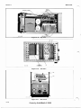
Figure 5- 9.
Top View
o
o
o
o
o
o
o
o
o
o
•
5-10
:::,,== o.��
Figure 5-10.
Side View
Figure 5-11.
Rear Panel
Scans by ArtekMedia © 2008
•
Scans by ArtekMedia © 2008
---1
---1
el27
-CRI47-CRI46-
r--
I
U}[]}--
el2.8
-CRU7-
R146-
-CRIIS-
R145-
G
---!
8---!
-R'35-
-RI34-
88
R149R151-
-CRI2l-
R143-
-CRI2l-
J
8
R122R136-
"
-
- RI50-
-U02-
- RI 44
.-J
-eRIOI ,
- RI42
-CRI os-
-CRIOS-CRIOS-
-CRIIO-
- RI20-
I
8
-CRIQ4-
-CI17-RI25-
e
- RI04 - RII1-
-CI04-
-RI26-
-RII4-
§
- R I 24 -
-RI38-
@
4
--- R I2S
-CI09-
- RIIO-eI29-
-U03-
8
-CRI43-
-CRI25-
@'
- RII3-
- R I 6 5-
-CRI24-
J2
-RI54-
RIG3
I
F-
-R162-
-CRI26-
8
-CI03-
- RII9-
-CRII4-
-CRI45-RIZ3-
RIOI
ON BACK
- RIOZ- - RI03-CI02-
-RI21-
e
"/
8
.-s-C I� I
-007- R I I 6- R l l1 -CRIO!-CI05- R I 1 50102
-CI06- RIIZ- -R I 4 1-ell!:)-
-CRI12-
r-
-CII9-
-CIOB-
-CRI I I -
-----7
-CRIOZ
-R!06-
-RI29 -
-CAI09-
-CRII,-
-- RI32
-ells-RI27 -
-CRI07-
-...,
- CI24-
- e l 2. l -
-CI22-
-CRII5-
-RI40-
- RI31-
-RII8-
-CRlle-
-RI39-
-eI23-
-CRIZO- - RI05-
R152-
el2S
-LIOI -
-CAI21- - R I 3 0 -
JI
ClCl-
el26
--RI55 ---
-CRI28-
-RI53-
,
-'-----.
\-CRI4o- I-- -
- RI64 -
-CR I27-
-CRI44-
-CRll9-
-CRI41-
RI59
-CRllB-
I
elll
_
CIIO
-CRI42-RI60-
- RI61 -"
-RI57-
- A I 58-
-CRllS-CRIJ6-
-CRllO-CAI29-
Q
�
-CRI34-CRI33-
,--,--,
-C RI32-
..
., ,
I
�------� .
-CRIJ7-
- RI56-
-CRI31-
•
,
•
hp
AI
Po,! No.
00467-66501
r
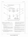
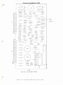
Figure 5-12. Printed Circuit Board (AI)
I
Parts Location
11
11
'
I
.
i
�
tIL--------------�tf-----------------. ----�I
,
Scans by ArtekMedia © 2008
,
"
· - - - - - - - - - - - - - - - - - - -- -
---.:
11
-
----,
__________________
.
__
-.J
>
i
,
1
i
i
--
!
"'
1" ' -------,
I'
[!"'J
If I
h ' ;o �
I
:
,1 h
6, 1;
�
I
•
I
I
b,_d' �
Scans by ArtekMedia © 2008
!
I
1
1
,,
1
I
1
,,
I,
I
,,
I
,
1
,I
. ,,1
I
,,
1
.___________
!
i
I-
�
!
;l
------_..
h
,.
1
I'
___ 0
1]
ji-
__.._______._...__
---
--
,
ii
;
r i' t ::
I�
::::::- " " - =-::='::"' '
__________
· i�
! !
.!
J
---
t,
!'
J
"
't"=-:.:.- - -r·
,
,
b
i-----i-;-' ;-
'
I
::!l a
, .r"
-
_
i
"
�il
,
�
--l-ff'
t;tti,-
--' -
'
---------- ----I
,
:' §'!
!!
I!
if
�.J
,
,
,
!l
li�,��!,�
,
,
!I
jl '1
j n
,
,
n
1; �� - -.:
l"-----��-l
h
ii n :
1
:
1
I
,,
1
I,
,.
_ _
_
��
,
,
��
j;;N'f--l-(!;iiH
,,
,
:
rr·.,----l-:,
, i!<..!""
. i'i � : :
�
,
: �§r,t
�
it
� � ;t '
:
,
,'""
,
,
!
II
:
" ,
_
J
SCHEMATIC MOTU
I.
2.
PARTIAL REFERENCE DESlG.'1ATIOSS AnE SllOWN. PREFIX
WlTII ASSEMBLY OR SUBASSEMBLY DESlGNATION(S) OR BOTH
fOR COMPLETE DESlGl'IATION.
COM POl'IENT VALUES ARE SIIOWN AS FOLLOWS UNLESS aJ'lllm.
WIlIE
1<OTEO.
rU:StSTANCE
IS OHMS
CAPACITANCE IN' MlCROFARAD6
•
-------
DENOTES MAlS SIGNAL PATI!•
------- DDOOTES n:EIlBACK PATH.
••
_____
OENOTES ASSEMBLY .
- - DEsan:s CDMPOS'EN'TS NOT
ASSEMBLY.
5.
MOUSTED 0'1
c::::::J DEl'OTES FRm., PANEl. MARKL"G.
�:::::"J DE.'>OTCS REAR PA.'1EL MARkll'G.
••
7.
�
DE.'>OTES SCREWDRIVER ADJUST.
RELAY KI IS SHOWN D£E.'>ERGlZED.
•
Scans by ArtekMedia © 2008
Scans by ArtekMedia © 2008
_0
..
>
§
£
,
!
s
�
�
.�
-
•
e �
!
•
,
Model 467A
PERfORMANCE C HECK TEST CARD
Hewlett-Pac.k.ard Model 467A
Power AmpliCler/Supply
Serial No.
Test Performed by
Date
CHECK
DESCRIPTION
1.
OC Gain Check
XIO
X5
X2
Xl
VAR.
2.
AC Accuracy and Gain Check
100 kHz
XIO
X5
X2
Xl
VAR-CW
TEST LIMITS
9 . 97 V to lO.OJ V
4 . 9 8 5 V to 5 . 0 1 5 V
1 . 994 V to 2.006 V
0 . 997 V to L 0 0 3 V
0
V to 10
V
INDICATION
TEST LIMITS
INDICATION
9 . 900 V to 10. 100 V
4 . 9 5 0 V to 5 . 0 50 V
1.980 V to 2.020 V
0. 990 V to 1.010 V
greater than 10 V
10 kHz
9. 970 to 10.030 V
4. 98S to 5 . 0 1 S V
1 . 994 to 2 . 0 0 6 V
O . tl97 to 1. OOJ V
greater than 10 V
XIO
X5
X2
Xl
VAR-CW
400 Hz
xlO
X5
X2
Xl
VAR-CW
9. 970 to 1 0 . 0 3 0 V
4. 985 to 5. 015 V
1. 994 to 2 . 006 V
0. 997 to 1 . OOJ V
greater than 10 V
1 MHz
XIO
X5
X2
9 . 0 0 V to l l . OO
4 . 50 V 10 5 . 50
1. 80 V to 2 . 20
0 . 9 0 V to l . 10
greater than 10 V
Xl
VAR-CW
3.
Distortion Check
1 kHz
100 kHz
1 MHz
4.
DC Voltage and Current Check
I V
ccw
I V
CW
2 V
CW
CCW
2 V
5 V
ccw
CW
5 V
IO V
CW
IO V
ccw
CCW
20 V
20 V
CW
5.
Load Regulation Check
No load
2 n load
V
V
V
V
SPECIFICATION
add < O . O I% (80 dB down)
add < 1% (40 dB down)
less than O. J V
INDICATION
SPECIFICATION
> - 1 . 000 V
> . 1.000 V
H 2 . 000 V
> - 2 . 000 V
> - 5.000 V
> + 5.000 V
> .. 10. 00 V
> -10.00 V
INDICATION
> -20. 00
>+20.00
V
V
SPECIFICATION
> .. 1 . 000 V
within 10 mV oC no load
Scans by ArtekMedia © 2008
INDICATION
Scans by ArtekMedia © 2008
Model 4S7A
PERFORMANCE CHECK TEST CARD (CONT ' D )
CHECK
DESCRIPTION
6.
Line Regulation Check
V line
115
126 . 5 V line
103.5 V line
7.
Output Impedance Check
500
8.
9.
kHz
SPECIFICATION
>-1. 000 V
within 10 mV of 115 V line
within 10 mV of 115 V line
SPECIFICATION
INDICATION
>0.8 V
Capacitive Load Check
Oscilloscope pattern
SPECIFICATION
Ripple and Noise Check
Supply Check
Amp1ifler Check
SPECIFICATION
< 1 . 77 mV rms
10. Current Limit Check
Shorted output
INDICATION
INDICATION
no oscillations
INDICATION
< 1 . 77 mV rms
SPECIFICATION
<800 mA
INDICATION
Section VI
Model 467A
SECTION V I
REPLACEABLE PARTS
6-3. Miscellaneous parts are listed at the end of
Table 6-1.
6 · 1 . I N TRODU CTION.
6-2. This section contains information for ordering
replacement parts. Table 6-1 lists parts in alpha
meric order of thelr reference designators and indi
cates the description , -hp- part number of each part,
together with any applicable notes, and provides the
following:
a.
Total quantity used in the instrument (TQ
column). The total quantity of a part is given
the lirst time the part number appears.
b.
Description of the part.
lions below. )
c.
Typical manufacturer of the part In a flve
digH code. (See Appendix A for list of manu
facturers. )
Manufacturer's part number.
d.
6·4. ORDERIN G I N FORMATION.
6-5. To obtain replacement parts, address order or
inquiry to your local HewleU-Packard Field Office.
(See Appendix B Cor list or office locations. ) Identity
parts by their Hewlett-Packard part numbers. Include
instrument model and serial numbers.
6-6. NON-LISTED PARTS.
6-7.
(SeeUstot abbrevia
To obtain a part that Is not listed, Include:
a.
Instrument model number.
b.
Instrument serial number.
c.
Description of the part.
d.
Function and location oC the part.
O&SIGHATORll
. ...."'
. bly
• motor
�
. "�
• mla< .'ee'"",\< po...
,
"
M
"
,
•
,
•
�
·OU'"
m
• Laalolo dlamete.
�
."'po'" (.j
. ...
�.
�
•
•
,
,
�
,
"
"
,
-110,,,,1)'
_ oapa<ltor
.-
-doJo, 'Ino
.,
,
,
'"
,
�
,
,
. .• lilt.,
•
boato<
•
jaok
• 1nI_.."" 01'0""
- .-1.,
_ 1nduc1O.
_ m_.
• IM<IIuIoaI po...
• ••
...,.
..
.
. ....
,
• ,,,,,"�...uodo
· ...,
.
....,
.
. t!>e•...w.>.
• ...
''''h
• ',..."'m
..,
••
tt
,
w
•
=
�
,
•
....nno<<>upl.
..ocwmb,obo. _
bulb.
·..,101.
. _..,
•
"""".", u. ....
Jam,pto>ldo.
_fIdo""'-do.
_ ..._.t
AQI'IJU;VIAT'ONS
"
,
<
...
.�
.-
._,
.-
"
" M
,=
".,
._,
,
,�
••
. 0.1
....
.......
• "pa<ltor
"
• .on",'
•
• .0010
11 1...
• '''''m
' ,,"
�
'.
•
•
_ mill' _ 10-3
..-
_blo-pOl. olope_
..-
.'ec''''y
'' llc
•
•
•
•
•
HelO ...,.."
IJaod
&.""�
•
_ .,..rd (od)
_"'.....
nlwn
,,
...
b
- 1<WIId
_
I
Mb
•
�.
bo....
(od)
• loo..., (18)
- IIIU<UI)'
_ Iooru (qel.
-...,
•
•
",U1I""'I"'
"" (0)
.....�.
0
(0) po.
.,
"'
,
"
10-S
...
",.p!>erU ' 10 loo.,.
mec<>'=<{o) ' ,<tOt ........
�
u
"
�
"
,m
• _...toe"" "
- ","""U",
-3
mlU" "" (.) ••0
• ...le.... • 10.8
•
•
m"'�(.)
• 10\110,
..__re (a)o IO·g
__"'.
• DOr"'"""" ..._
.• ..,malt,. -"
_ _U.. _.11... ..'"
tu", "'_..."•
'• co-
onlotLo-nl)
®
""''"
-I
.0110
.10
_
,
00
(0) _ 10""'
-• _ _...tolr �_-
_ ...
>IOOeeIHId
.M.
. _ (a)
_ <>rior ..,. dooorlpll""
• ""talolo dla
...... .
,
.....
• p" nted c,....U
..
"
p'cofl.rod (a) • lo-n
.01 .....
• peot 1In"...... .
• pari "
• pOoIUOo (o.j
•
'OP""""" 1apO.
"'" flm ...."" IU",
...
, ..
,
. "'.
• plU"",
• II,pbo<U
. ,-' ....'
.
�
M.
....,.p.....ted
"'rod (.)
•
loon.
""""'to.
•
'U.
Ob
�
. 10"
,
..
•
_.
• IIJI""", (a) _ 10" ohm.
• kIl0h0...
· ._UloIo
• ooone<tIoa
depoolled
. _.-pal._.-
-
Imp_led
_ ...,.,odeo<u'
• '->la""'" (od)
••
W'
�
....
..
"
••
,-
•
• pair·,,.....
·_.U.........
• ,..,._to_pu>
po..... "'" mU!"'"
• p....."'" ("'mpo"''''''
.otIll.",ol. ,_ to...
•
OIabUIIJ. o..wo. 101_
._,
,
�
•••
•
-'
•
· "...,,"
• ,_WIt
· ....,.-......-.....'"
.�"
. ..,..."'"
-'ka> {o)
•
· oO\<OOI
"
"'M
_ 011'"
- oillBle-pol. doub,._
-
- olop._poI.e .ilIBle-
"
"
TI02
'.
�
=,
•
_.
�-
-
• lanll.lom
• ,._"''''... .ootlf..1ont
nh". d1""",,"
•
.
• U'
._"
t.ote.....
...
• """..o,
.��
•
•
-.01, (0)
• tJ",...U", ""'"""",
won..., .01..
",
• ...,.,.
101
•
•.
-
...., o:urront '-'.,.r
• .u
W
.wa..
./
...
./.
-
�-
• .'ll>
(0.)
- worl<hl& "'••,
.. .01....
_ w.tI>ou,
- .......
, .•
opU",,,,,, ""UO OO'Kted
0' 'le""". •'.race
... _1
"".. _.. (po
loo "",mod)
- ""."_rd l)'l>o """'bO, ...� (""'octed
'" _101 typo)
� "' N.""'"
Scans by ArtekMedia © 2008
6·1
Scans by ArtekMedia © 2008
section VI
Table 6-1.
REFERE:-'CE
DESIGNATOR
-hp
PART NO.
Replacl'abll' Parts
TQ
00467 �66S01
1I1ode! 467A
OESCRlPTIO�
Assembly:
board, amp and p<)wer supply,
MFR
MFR
PART NO
-hp-
00467 -66501
C: bd, 0. 1 IlF ±S%
C: !xd, cer die, I section, S. 6 pF ±O. 25
pF, 500 vdcw
C: fxd, cer die, 1 . O > l F ±20%, 25 vdcw
C : fxd, cer dle, O. t ).lF +80% -2dl, 50 vdn'
56289
72982
192PI0452
301 -Oll-C OH 0-569C
56289
56289
5CI3
5C50A
C: fxd, dlpped mica, 47 pF ±S%
C: bd, d
ipped mica, 200 pF ±5%
c: fxd, cer die, t . O >lF ±2o%, 25 vdcw
00853
00853
56289
RDM1SE47OJ3S
RD:-.115F20IJ3C
5C>3
inCludes:
CIOI thru C129
CRIO! Ihru CRt47
LIO! thru L I 03
QIOl thru QII2
RIOI thru RI65
AICIOI
AlCI02
0170-0019
0150-0060
2
,
AICI03
AlCI04
0160-0127
01SO�0121
,
,
AICI05
AICIOO
AICI07,
AICI08
AIC109
0160�0182
0140�0198
0160-0127
2
,
0160-0182
C: !xd, dlpped mica, 47 pF ±S%
00853
ROMt5E47OJ3S
AIClIO
0180-0306
56289
34Q307HOI5FJ4
AIClIl
AIC112 thru
AICI14
AICI15
0180-0110
C: fxd, AI elect, 300 >I F -10% +100%, 15
vdcw
C : fxd. AI elect, 80 IlF, 75 vdcw
Not assl�ed
56289
type 410 033191
0150-0091
C : fxd, cer die, 1 . 5 pF ±0 . 2 5 p F , 500 vdc",'
72982
301-011-0KO 159C
A1CI16
A1C1l7
A1C118AIC1l9
0140-0176
0150-0093
0150-0058
0150-0121
A1CI20
A1CI21
AIC122
AICI23
0160-0127
0150-0063
0140-0146
I
I
A1C124
0132-0004
I
AIC12S
0180-0039
2
AIC128
AICI29
0180-0058
0150-0093
AICRIOl.
AICRI02
AtCRI03
AICRI04
AICRI05,
A1CRI06
1901-0150
2
1901-0040
1902-0048
1901-0025
2
5
20
AICRI07
1901-0050
I
AICRIOS Ihru
AICRIIO
AICRlll thru
AICRI13
AICRI14
1901 -0025
AICR1I5
AICRI16,
AICRII7
AICR1I8
AICR1I9
AICt26
AIC127
'-2
0180-0058
0180-0039
1910-0016
,
2
3
3
pF
±2%
C: fxd, dipped mica, l OO
C : txd. O . O I ). l F +80% -2 0'{" 100 vdcw
c: f:oo;d, 2. 2 pF,
C: fxd, cer die, O. I >IF +80% -20%, 50 vdI''''
00853
91418
ROMI5FIOIG3C
TA
obd
56289
5C50A
Not assigned
C: bd, cer die, 1 . 0 >I F ±2o%, 25 vdcw
C: (xd, cer die, 10 pF ±O. 5 pF, 500 vdcw
C: fxd, mica dle, 82 pF ±5%, 300 vdcw
56289
72982
14655
50>3
301-011-COGO 1000
Cot5F82OJ
72982
53S-009-4R
56289
56289
56289
032697
028110
032697
C : Ixd, 0.01 >I F +80% -20%, 100 vdcw
C; !xd, elcct, 50 >IF -10% +100%, 25 vdcw
56289
91418
028110
TA
O1ode: SI, low leakage, low capaCitance
-hp-
1901-0150
Dlude: Si, 30 mA at +1 V, 3 0 plv, 2 pF , 2 n
Olode: breakdown , 6.81 V ±5%, 400 mW
Diode: S i , 50 mAat .I V , 1 0 0 piv, 1 2 pf
-hp-hp-hp-
1901-0040
\902-0048
1901-0025
OIode: SI, 75 V Working, 2 pF, 2 ns, 200
mAI... 1 V
Diode: SI. 50 mA al .I V , 100plv, 12 pF
-hp-
1901-0050
-hp-
1901-0025
Oiode:
C: var, trimmer, 0.7 to 3 pF, terminal
spacing
C: fxd, elect, 1 0 0 " f ' , 12 vdcw
C: fxd, elect, 50 >IF -10% +100%, 25 vdcw
C : fxd, elect. 1001lF. 12 vdcw
-hp-
1910-0016
1901-0040
'"'
I)\ode: Si, 30 mA al +1 V, 30 plv, 2 pF, 2 n
-hp-
1901-0040
1902-0048
1901-0025
Diode: breakdown, 6.81 V ±5%, 400 mW
Diode: SI, SO mA at . j V, 100 piv, 12 pF
-hp-hp-
1902 -0048
1901-0025
1902-0048
OInde: breakdown, 6.81 V ±5%, 400 roW
Not assigned
-hp-
1902�0048
Ge, 100 n,AaL ...0.85 V, 6 0 V work
Section VI
Model 467A
Table 6-1
REFERENCE
DESIGNATOR
AICRI20,
A1CR121
AICR122,
A1CRI23
AICR124
AICRI25 thru
A1CRI28
-hpPART NO.
Replaceable Paris (Cont'd)
DESCRIPTION
MFR
1901-0025
Diode: Si, 50 mA at +1 V. lOO piv, 12 pF
-hp-
1901-0025
1902-0048
Diode: breakdown, 6.81 V :l:5%, 400 mW
-hp-
1902-0048
Diode: breakdown, Si, 33.2 V :l:5%, 400 m" -hpI
-hpDiode: S, 200 plv. 0. 5 amp
1902-0186
1901-0026
Diode: SI, 50 mA at +1 V. 100 piI'. 12 pF'
-hp-
1901-0025
-hp-
1 902-3296
-hp-
1901-0026
1902-0186
1901-0158
TQ
,
•
MFR. PART NO.
AICRI29 thru
AICRI34
1901-0025
A1Ct(135
1902-3296
A1CR136 thru
AICRI39
A1CRI40 thru
AICR142
1901-0158
Ulode: breakdown, SI 33.2 V :1:2%. 400 mW,
glass
Diode: Si. 200 piv, 0 . 5 amp
1901-0025
Diode: SI, 50 mA at ... 1 V. 100 piI'. 12 pF
-hp-
1901-0025
AICR143
1902_3296
-hp-
1902-0186
AICRI44,
AICRI45
AICRI46.
AICR147
AIJIOl
1901-0025
Diode: breakdown, SI, 33.2 V :l:5%. 400
mW
Diode: Si, 50 mA at ... 1 V. 100 piI'. 12 pF
-hp-
1901-0025
AILI01,
AiLI02
AILI03
AIQI01
AIQ102
AIQI03
AIQI04
2
1902-3139
2
Diode: breakdown. 8 . 2 5 V
-hp-
1902-3139
U61-0131
1251-0324
9140-0137
,
,
2
00373
00373
-hp-
69026-1165 (red)
69026-1064
9140-0137
9140-0096
1854-0023
1854-0019
-hp-
3
2
Connector: female
Connector: male
Coil: fxd RF, 1000 J.I. H:I: 5%, dc current
raUng 135 mA
Coli: fxd RF, I J.l.H :1:10%
i
TSfR: NPN S
TSfR: NPN SI
TSl'R, NPN Si
TsrR: NPN Si
9140-0096
1854-0023
1854-0019
TSTR: PNP Si. type 2N2904A
TSTR: NPN Si
TSfR: PNP SI. type 2N2904A
TSTR: matched pair. two 1854-0023
transistors with VBE matched
-hp-hp-hp-hp -
1853-0012
1854-0022
1853-0012
1854-0046
TSTR: NPN Si
TSTR: NPN Si. EtA type 2N3053
-hp86684
1854-0023
2N3053
met Urn, 392 K ohms *1%. 1/4 W
metal-oxide Urn, 3900 ohms :1:5%,
19701
75042
07115
CFl/2C
CBe T-O
C20
obd
obd
metal-oxide Om, 10 K ohms :1:5%,
07115
C20
obd
R: bd, met flm. 2.05 K ohms *l/2%. ,I.
W
R: bd. comp, 2000 ohms :1:5%. 1/4 w
Not assigned
76055
CEB T-2
obd
01121
CB2025
07115
C20
obd
metal-oxide Um. 3300 Ohms :1:5%.
07115
C20
ob'
met flm, 82 ohms *5%. 1/2 W
metal-oxide flm. 3300 ohms :1:5%.
-hp07115
0756-0026
C20
ob'
metal-oxide flm. 4700 ohms :1:5%.
07115
C20
ob'
1854-0023
,
1854-0019
2
AIQI05
AIQI06
AIQI07
AIQI08.
AIQI09
1853-0012
1854-0022
185�-00!2
5\180-9023
2
AIQ110
A1QIll,
AIQ1l2
1854-0023
1854-0039
2
AIRIOI
A1RI02
AIRI03
0696-0076
0757-0787
0758-0045
•
AIRI04
0158-0006
3
AIR105
0696-0072
2
AIRI06
AIRI07 thru
AIRlO9
AIRIIO
0683-2025
,
0758-0007
,
R: fxd, metal-oxide flm, 150 ohms i5%.
1/2 w
AIRIIl
0756-0010
2
AIRIl2
AIR1l3
0758-0026
0758-0010
,
AtR1l4
0758-0005
3
R: fxd.
1/2 W
R: fxd,
R: bd,
1/2 W
R: fxd,
1/2 W
,
,
2
R: bd,
R: fxd.
R: bd.
1/2 w
R: fxd.
1/2 W
carb flm. 2000 ohms ±5%. 1/2 W
-hp-hphp
_
_
-hp-
1854_0023
1854-0019
'-3
Scans by ArtekMedia © 2008
Scans by ArtekMedia © 2008
Secti<.lJl VI
Tahle 6-1.
HEF EIUSCE
DES1C'-':A TOl{
- hp-
PAR.T KO.
AIR115
0758-0045
AIR116
0758-0005
A1R117
0758-0047
AlRl18
0758-0045
R.eplaceal.)le Pans (Cont'd)
M FR. PART NO.
DESCRIPTION
MFR.
fxd, metal-oxide flm, 3900 ohms 1:5%,
1/2 W
H: fxd., metal -oxide flm, 4700 ohms ±5%,
1/2 W
n, fxd, metal-oxide flm, 7500 ohms, 1/2
W
H, [xd, metal-oxide rim, 3900 ohms +5%,
07115
C20
ob'
07115
C20
obd
07115
C20
Db,
0 7 1 1 :,
C20
obd
07115
C20
obd
120 ohms ±5%.
07115
C20
obd
metal-oxide flrn, 100 ohms ±5%.
07115
C20
obd
rnetal-oxide flm, 470 ohms ±S%,
07115
C20
ob<!
01121
07115
CBl015
C20
obd
07115
C20
obd
011Z1
EB330S
76055
75042
76055
3 MOL
CEB T-O
CEB T-2
obd
76055
CEE T-2
ob<!
19701
CF 1/2
obd
-hp-
2100-0395
07115
C20
obd
07115
C20
obd
0711S
C20
obd
07115
C20
ob'
H, fxd. metal-oxide flm. 75 K ohms ±5%.
07115
C20
obd
n, fxd. metal-oxide Om, 33 K ohms .1.5%.
07115
C20
obd
n, (xd. metal_oxide flm. 68 K ohms ±5%,
07115
C20
obd
75042
CEB T-9
obd
76055
CEll T-2
obd
76055
CEB T-9
obd
07115
C20
obd
07115
C20
obd
-hp-
2100-0898
TQ
H·
2
Model 467A
1/2 W
A1R119,
A1R120
0758-0053
2
AIR121
0758-0013
I
A1H122
0758-0024
3
A1R\23
0758-0029
I
A1R124
AIRl25
0683-1015
0758-0003
I
I
fxd,
1/2 W
H, [xd,
1I2 W
H· fxd..
1/2 W
H· bd,
1/2 W
H:
metal-oxide flm , lOO K Ohms ±5%,
metal-oxide flm,
H· bd., comp, lOO ohms 01;;5%, 1/4 W
[xd, metal_oxide flrn, 1000 ohms .1.5%.
H,
A1R126
0758-0070
2
A1Rl27
0686-3305
I
1/2 W
H· [xd., metal -oxide flm , 1200 ohms ±5%.
I/Z W
H: [xd, comp, 33 ohms .1.5%, 1/2 W
AIR128
A1RI29
AIR130
0698-0069
0757-0756
0698-0073
I
H, fxci, l!JOO ohms
I
H,
I
-15%. 3 w
!xd, met flm. 13 K ohms .1.1%. 1/4 W
H, !xd, met Bm, 1 6 . 2 K ohm s +1/2%, 114
obd
W
w
A1R131
0698-0072
A1RI32
0727-0312
I
A1R133
2100-0396
I
AIRI34
0758-0006
A1J{135
0758-0079
I
AIR136
0758-0008
I
A1H137
AIR138
0758-0017
H·
I
[xd, met flm. 2 . 0 5 K ohms ±1/2%. 1/'
n, [xd, carh flm, 9 M ohms :1-1%. 1 W at
70oe, 1/2 W at 12SoC
o,
H· var, ww. \in taper, 10 K ohm s ±20""
IW
n, [xd, metal-oxide flm, 10 K ohms :t5%,
1/2 W
H: [xd, "metal-oxide flm. 30 K ohms -t5%.
1/2 w
H,
[xd, metal-oxide flm, 390 ohms i.5%,
1/2 W
Not assigne d
H:
[xci, metal-oxide flm , 1500 ohlll s 015%
1/2 W
A1R139
0758-0077
I
1/2 W
A 1H140
0758-0049
I
1/2 W
A 1IU41
0758-0076
I
AIR142
0698-0070
I
A1H143
0698-0074
I
A1R144
0698-007:1
I
A1H145
0758-0038
I
A1RI46
0758-0047
AlH147,
AIRI48
2100-0898
6·4
1/2 W
H: fxd. met Om, 1. 87 K ohms .!.l/2%.
1 /4 W
H, fxc!. Illet flm , 90. 9 ohms ±l%. 1/4 W
R: {xd, nlct Hm, 1 7 . 4 K ohm s :t-1/2r". J/4
W
n, (xci, metal_oxide flm. 9100 ohms ±5'O.
112 W
H· [xd, metal-oxide flm, 7500 ohms. 1/2
W
2
n, var, Ilrec
","W,
500 ohms ±5f1.
Section VI
Model 467A
Table 6-1
R E FERE:-<CE
DE:)IG:-<ATOR
-hp-
PART NO.
TO
DESCRlPTION
/I.'FR
,
R: fxd, metal-oxide flm, 910 ohms :1:5%,
1/2 W
R: fxd, metal-OXide flm, 3900 ohms ,,5%,
1/2 W
R: fxd, metal·oxlde flrn. 1200 ohms :1:5'\.
1/2 W
R: fxd, metal·oxlde f1m. 1600 ohms :1:5%,
1/2 W
07115
C20
obd
07115
C20
0""
07115
C20
0",
07115
C20
0,",
R: fxd. metal-OXide flrn. 3000 ohms :1:5%,
1/2 W
R: fxd. ww, lOO ohms :1:3%. 5 W
R: fxd, comp, 47 ohms :1:5%. 1/2 W
R: fxd, rnetai-oxlde Um. 22 K ohms :1:5'\.
1/2 W
07115
C20
0",
00213
01121
07115
1500S
EB4705
020
obd
R: fxd, metal-oxIde flm, 220 ohms :1:5%.
1/2 W
R: var, Iln taper. ww. single section. 1
ohm :1:10%, 2 W
R: fxd., metal-m(lde flm. 5100 ohms ±5'\,
1/2 W
"' "'d, metal-oxide flm, 910 ohms :I::S%.
lW
07115
C20
obd
-hp-
2100-1415
07115
C20
0,",
07115
C"
oOd
07115
C20
0,",
-hp·
2100-1415
07115
C20
obd
07115
C20
obd
-hp·
00461-61901
56289
00853
00853
obd
5Ct3
RDM15F910F3C
RCMlSE410J
15042
15042
1S042
75042
CEBT"O
CEB T-O
GEB T-O
CEE T-O
obd
obd
obd
obd
75042
-hp-hp-hp·
GEB T-O
0812-0090
0812-0089
0812-0088
obd
-hp-
0812-0087
-hp·
3100"()806
-hp·
00467-66503
AIRI49.
AlRI50
A1Rl51
0758-0068
A1R152
0758-0070
AIR153
0758-0083
1
AIRI54
0758-0035
1
AIRI55
AIRI56
AIR157
08t1-0939
0686-4705
0758-0020
1
1
1
A1R158
0758-0015
1
AIR159
2100-1415
,
AIRI60
0758-0037
1
AIR161
0761-0013
1
A1RI62
0758-0083
,
AIRI63
2100-1415
AIRI64
0758-0004
AIR165
0158-0005
A'
0758-0045
00461-61901
Replaceable Parts (Cont'd)
1
1
R: fxd, metal-oxide flm, 68 ohms :1:5%,
1/2 W
R: var, Iln taper. ww. single section, 1
ohm :1:10%. 2 W
R: fxd, metal-oxide Urn, 2 . 7 K ohms ",s%
1/2 W
R: fxd, metal-oxide fim, 4700 ohms ",5'\.
1/2 W
Assembly: switch, amp and supply, '"eludes:
C201 tbm C203
R20 I thru R209
A2C201
A2C202
A2C203
0160-0127
0160-0335
0140-0039
A2R201
A2R202
A2R203
A2R204
0698-3143
0698-3144
0757-0148
0698-3144
A2R205
A2R206
A2R207
A2R20B
0757-0146
0812-0090
0812-0089
0812-0088
A2R209
A2S201
,
,
,
,
,
PART NO
52. 3 K ohmll .201%, 1/4 W
8.87 K ohms :1:1% 1/4 W
4.15 K ohms :1:1%, 1/4 W
8,87 K ohmll :1:1%, 1/4 W
R,
R,
R,
R,
fxd.
fxd,
fxd,
fxd,
1
R,
R,
R,
R,
fxd, met flm, 4.75 K ohms :1:1%,
!xd, �, S.0094 K ohms .:to. 05%,
fxd, �, 5.0132 K ohms to.05%.
,,� �, 15.046 K ohms to.OS%.
0812-0087
1
R lxd.
3100-0806
,
Switch: rotary, 3 sections
00467-66503
,
Assembly: board,
C301 thru C307
A3C301
A3C302
A3C303
0121-0060
0160-0161
0121-0061
,
,
,
C: var, cer, 2 to 8
C: fxd, 0.01 jJ F :1:10
C: var, cer, dlllC, 5. 5 to 18 pF. NPO. 300
-hp·
56289
4hp�
0121-0060
192PI0392
0121-0061
A3G304
0170-0066
,
vdcw
G: bd, 0 . 027 jJ.F :1:10%
56289
192P27392
A3C305
0121-0046
,
C:
-hp-
0121-0046
A3
1
,
var,
�,
0,",
S20l
ie, 1. 0 jJ F :1:20%, 25 vdcw
C, fxd, eer d
C , "'d, dipped mica, 91 pF :1:1%
C, fxd, molded mica, 47 pF ±5%
met flm.
met flm.
met flm,
met flm,
/l.1FR
1/4 W
1/4 W
I/� W
1/� w
25 K ohms .:to. 05%. 1/4 W
ac
Input, includes:
R301 thru R303
�
cer die, 9 to 35 pF
6-5
Scans by ArtekMedia © 2008
Scans by ArtekMedia © 2008
Section VJ
Tab]e 6-1
REF£lO ::-;CE
IJE$! (;" ,\ TOH
-hJl
PAHT NO.
Mod('] 461A
Rep]aceab]e Parts (Cont'd)
DESCRlPTlON
TO
MFR
00853
56289
A3C308
A3C301
0140-0202
0170-0019
C: fxd, dipped mica, ]5 pF :1:5%
c: bd, O. 1 ,. F :1:5%
A3R301
A3R302
A3R303
0727-0858
069S-0071
0757-0787
R: bd. dcpc: rim. 3.48 M ohms :1:1%. 112 W 0000'1'
94459
R: bd. (!epc flm. 1. 58 M ohms :1:1'\
7S042
R: (xd. met Um. 392 K ohms :l:1�. 114 W
00467-66502
A4C401.
A4C402
A4C403
0180-0136
,
0150-0012
,
A4R401
0758-0080
A4R402
0758-0025
A4R403 ttoru
A4R405
0699-0006
4
MFR
PART NO
RDM15C150J5C
192Pl0452
CDl/2MR
eve
CEBT-O
ASS('mbly: board, output amplifier. In
cludes:
R401 thru R411
C401 1hru C403
-hp-
00467-66502
C: bd. AI eled. 10 j.l.P -10'\ .100'1,
50 vdcw
C: (xd. disc. cer die. 10.000 pP ±20%.
1000 vdew
56289
40Dl93A2
71590
13C Disc.
obd
R' bd. metal-oxide Om. 75 ohms ±51"
1/2 W
R: bd. metal-oxide f\m. 160 ohms :1:5'\,
1'2 W
R: bd. comp, 4 . 7 ohms ±to'"!'. 1 W
07115
C20
obd
07115
C20
obd
01121
GB47Gl
R: !xc. metal_o"ide flm. 68 ohms :1:5%,
07115
('20
obd
07115
C20
obd
01121
EB27Gl
01121
07115
CB47GI
C20
72962
301-011-COHO-479C
56269
038530
56289
5CSOf\
71590
13 C Disc.
71590
00853
obd
MR406
0758_0083
MTH07
0758-0024
A4R40S.
A4R409
MR410
MR411
0699-0001
0699-0006
0758-0006
R: fxd. comp, 4 . 7 ohms :1.10%. I W
R: bd. metal-oxide (lm. 10 K ohms :1.5%.
1/2 W
Cl
0150-0089
C2.C3
0180-0359
C4. CS
0150-0121
e'
0150-0012
C: fxd. eer di('. 4. 7 pI" :1:0.25 pP. SOD
...dcw
C: fxd. AI elect, 1000 I'F -10% �75'l,.
15 vdew
C: bd, cer die. O. I /l P ..S01, -20%. 50
vdew
C: bd. disc. cer die. 10.000 pF :1:20%.
1000 vdcw
C7. C8
CS
0160-0195
0140·0149
OSI
2140-0015
L'l.mp: (!"Iow, high brightness neon. NE-2H
bulb T-2
-hp-
2140�00I5
2110-0020
Fuse: e"rtr[d�. 0 . 8 'lmp. ghss body.
slow-blow
71400
MOL 8 '10
1251-0135
Connector: P. '::. . 15 tunin!!: fork tvp('
contacts
COnJl('ctor: P. C . . 18 tunIng fork type
eonl'lcts
BindIng post: r('d. without solder turret,
brass
Binding post: black, without solder turret.
000""
so 615 UR
OOOX)(
SO-618 UR
-hp-
1 5 10-0008
-hp-
1510-0009
-hp-hp-
0340-0099
0340-0100
h\l
1510-0008
-hp-
5060-0625
1510-0009
J\
112 W
R: fxd. metal-Oxide f1m. 100 ohms ±51.
,
,
,
I
J2
JJ
1 5\0-0006
2
1510-0009
,
0340-0099
0340-0100
\510-0008
5060-0625
1510-0009
5
4
]/2 W
R· bd, comp. 2 . 1 ohms :1:101-. 1/2 W
C:
C:
bd. c('r die. 1000 pP :1:20%, 250 vacw
hd, mic'!. die. 470pF :1:5". 300 vdew
brass
Insulator: 'lnti-rotation boss (out('r)
Insulator: bi1ding post. grey pi1.stic (Inner)
Binding post; red. without solder turret.
brass
Ass('mllly: (()11nedor
Binding post: black. ",ithou! solder turret.
brass
0-'
0",
obd
obd
-
-
-hp�
D15F471J
obd
obd
Scctiun \' 1
lIIodel 467A
Table 6-1.
REFERENCE
DESIGNATOR
-hp
PART KO,
Replnrenble Pans (Conl 'd)
M FH
DESCRlPTION
7.
\',\H I' :-lO
J4 (Cont'd)
0340-0099
0340-0100
Insulator: "nti-rotatlon boss (outer)
Insulator: binding post, �rey plastic (:nner)
-hp-hp-
0340-0099
0340-0100
J5
J6
1251-0148
-hp-
1251-0148
J7
J8, J9
1251-0473
1250-0118
Connector; pwr, receptacle, 3 pin male
Not assigned
Connector: P. C• • 12 ribbon type conllrts
Connector: series BNt; bulkhead re('ep
tacle
_bp_
91737
1251-0473
6427
K>
0490-0147
-hp-
(l490-O147
LI, L2
L3
QI thru Q4
Q5 Ihm Q8
R>
R2, R3
R.
R5
9140...0 136
9140...0106
1854-0037
1850-0098
0684-3331
0811-0940
2100-0352
2100-0993
Relay: con resistance. 900 Ohms. 750
ohms mln
Coli: fxd RP, 22 /lH ±10%
R6
0758-0024
R7
0727...0018
SI
..
3101...0036
3101-0033
TI
I
,
,
I
•
•
I
2
I
I
-hp-
9140-0136
Coil: fxd. 0 . 4 7 /lH .i20'\.
TSTR: NPN Si
TSfR: PNP Ge
R' fxd, comp, 33 K ohms lIO%. 1 '4 \"
R: fxd, WW, 60 ohms :t3", 50 W
R: "ar, 5 K/SO K Ohms tS". 2 W
R: var, ww. 10 K ohms ±1011. 5 W
-hp-hp-hp01121
-hp-hp-
-hp-
9140-0106
1854-0037
1850...00 96
C'03331
061 1 -0940
2100-0352
2100-0993
R: fxd, metal-oxide flm, 100 ohms .iSh,
07115
C20
ohd
00001'
CDl/2PR
Dud
SWitch; toggle, SPST, 3 amp. 250 vac-de
Switch; slide, DPDT, non-shorting O. 5
amp 125 vdc, 3 amp 125 vac, 115/230 V
_hp_
-hp-
3101-0036
3101-0033
9100-0307
Transformer;
-hp-
9100-0307
WI
8120-0078
Assembly: cable. power, smooth blaek
extra limp, 7. 5 ft Ig, eet
-hp-
8120-0078
XFt
1400-0084
Holder: fuse, extractor post type, for
single 3 AG cartridge fuse
-hp-
1400-0084
1/2 W
R: fxd. carb IIm, 40 ohms ,,1%, 1/2 W
power
MlSCE LLANEOUS
5040...0235
00467-01201
00467...01202
1410...0052
Base: lampholder
Bracket: heat sink
Bracket: rear
Bushing: pot, 0.435" OD by 0. 438" Ig,
nickel plated
-hp-hp-hp-hp-
5040-0235
00467·01201
00467-01202
1410-0052
00467-61601
Cable assembly;
Chassis
-hp-hp-
004.67-61601
UU4lj'{-UO 10 I
bottom, 5 x 1 1 SM
-hp-
5000-0714
hp
UU41j'I-UUlUl
5000-0714
Cover:
mai n
5000-0703
5060-0712
,
I
Cover: side. 6 x 11 Sl\]
Cover: top, assembly. 5 x 1 1 SM
-hp-
5000-0703
5060-0712
5060-0727
5060-0703
,
,
Foot assembly: third mod
Frame assembly: 6 x 1 1 S�l
-hp-hp-
5060-0721
5060-0703
00467-21 1 0 1
1205-00ll
1205-0041
5040...0700
I
5
I
,
Heat sink
Heat sink: TSTR
Heat Sink: TSTR
Hinge
-hp-hp-hp_hp_
00467-21101
1205-0011
1205·0041
5040-0700
5040...0425
1200-0043
4
Insulator: BNC panel
Insulator: TSTR, mtg, anodIZed Al pl�te
-hp-hp-
5040-0425
1200-0043
Knob; bar
-hp-
0370-0077
0370-0077
•
Scans by ArtekMedia © 2008
-
-
Scans by ArtekMedia © 2008
Section VI
Table 6-1
REFERE:NCE
DESJGNATOR
-hp-
PART NO
Model 4 67A
Replace:lble PartS (Cont'd)
TQ
DESCRIPTION
MFR
MFR. PART NO
MISCELLANEOUS!
Cont'd)
6-'
0370-0084
1
Knob: round, back, 5/8"
dl
am shaft
�40-o234
1
Lampho\der
00467-90003
1
Manual: serial prefix
00467-00201
00467-00202
1520-0001
1
Panel:
1
2
diam. for 1/4"
444
front
0370-0084
-hp-
�4D-0234
-hp-
00467-90003
-hp-
00467-00201
00467-00202
1520-000]
Panel: "u
Plate: mtg. bakellte, oval shape
-hp-
-hp-hp_
5020-0700
00467.24701
1490-0031
1
2
Spacer: cab. third mod
$pacer: heat sink
stand: thIrd module till. stainless steel
,od
1200-0080
•
Washer:
1
-hp-
Insulating. hard anodized Al.
ID for 10-32 screw
-hp-
-hp-
5020·0700
00467-24701
1490�31
-hp·
1200-0080
CODE LIST Of MANUfACTURERS
Iollo�"1 eocIe ....
m bll n IOn fl'Om lb, Federal �pply Code for ....
f
ae
...
tu.. r. C1taloct"lIl"'.:JbO<>U Ht_1
{Nam, to C<:Idel &rid 114_2 (Code to Name) aDd the.r latest *"pplem'nta. The data of " vH,len and the date ef IIHt
.uppl.menbJ 1U6<I ap�ar at the bottom of each p..-,. "'lphabet\�� cod<Il h
... . bull arbllrarU, ....o&""d
..
to
euppllers not app"arl"l In 0.. JH nandllokll
o .
ThII
........,
..
100DO U . I � e.....
OOIl' .te., ("w.. ,,,
OGlll I". [1"1"'1<' Cor,
00111 C••<o 10<
1101)1 M••,I,.I
001"
001/1
oon,
IIOIIt
00111
001l!
oonl
�"
.."h".!U.I.
SiI" '"
P•.
h'�" I". �.,.
K...I �"I,
�""ID' Co., I".
�"I". tI,
�"o,,, C."
PO"""', C...
e. II.. , C.',!.
V.II" $".... ". Y.
n.",
�'", � J
h_ 8.llorl. ....
"""n"I. "
b, IO,
A"<,,It 1" •• COl.
8•••10', � J
�or"'''. ['1'"'' 'l lUor.I,,'''. I""
8ort" II••• ,,,.
!o'I'"' £'1<1", C.. '"1''' Pi>
P,,''''. I C.
00111 Coo ['1 .. ..".1 ,.
C,II .I IU"I'I. C""
00111 C"I [ M.I... COl'
lOO A'I.I.., '"" I
0011! •""1",, I".
l"" llI•• , " J.
01001 C ..ml E I.. I", c.,. C .....I" gUI
�tlo. ,,,10,(0 e•.
AU•• •""., e.
o l m l,lt.ol.I",,,... 1«mll T U 50••' ....<1... , I"
01191 1 .... 1.." ••••10. 1 0•••
o lOO!
11111
1",.,,,., P,.do<1O DI.
n. � ,.,," MI, C.
P."I" ".1.,., I.,
Oil'!
Olm
01110 G••,�.. . B,••. SII' C..
olm ..""I Cor,
01111 P.I" ,01" '''''1 C..
01111
Olili
mu
miC
Olll!
011Jl
Ollll
02U!
H..... f.II•. M,Y
9",1\••. �...
�"...I... I••.
8.... ,' Mill., C.li!.
lO" ;"., COI,I
O&U.. T....
Atl".". c, ••
�. . h,., Col.'
h� U'I. " . I
�"II.,•. !U.
,..11 Cl.... C.III,
SIO,,,IIO., K.Y.
f""",1O C.., ,1&. ..,,,
LOll 9,"CJo. N . ) .
'U.,,,. S'I. .I., I"
Col, R,��" ..I PI",,<o "" ,
$.",,, .. . C" ,I
"9""I·B", E'''''''''' Cor"
B"U... _, Ill.
R .. .. C"9. • 1 .'."<0. I....... ""',
So.""I,,, _ J.
... ut""" D",
�."'". Co, 01 h.",o, lot
HOIk," E" """" C.
H..... I""
D•• C.
01i \.I,�".\. C...
\.I. ,........ Cohl,
�'."I.. � J
OlSOI G. E l.. .".,."" PlO' D,,� I,'.. ... . N. V
0.,1", OIl.
il/61 A,.. .u,.,. ' 1..1 C.,
C...t". C.I,I
oml EIU., COl"
L .. AOI"". CII.I,
GlUI P,,'., I. ., e.
Ollll r". ...... [I."", c....
,.1..11016. M...
c.;" K..,lO, � J.
olln P,,,,.,. A....'" e.
I"
0l!1I :;"1" C•.. P,ul 0"
f,...,.. PI"I
h.""H•. � I .
O'OH �,,,. H." 010 Htlt.., [ 1.. 1 C.
H.lllori. C....
l.. �t'I.. I I•. " J.
0�01l ,..". CO"
efl.' �",. � y ,
0'0'1 A,,, E',W.." ,0<
Wf,lI. 8..,., f.C,
OU!! H'·Q 0.'1'1'. o ! A"""
01)1' 9 ..",... P.,,, h•• e.
IU.I"I. III
OI�O. g,.., 0.."". , I H ••t'II·P ,,' ''' C.
POl. All., C.1 It
O'UI SII.". ['0< 1'" P"htU. K I ".....
p",,, D.,
h"I". YII• . C','!
0.1/1 0..01. E'I', I".
Col .., C " " '0101.
01111 �'I'(';', 10<
1.. ,,,.0,,1,, Pto' Oi,
PI••"., A.."..
0'111 f,II... Co. • '" ..u". O.. ,
C.I", C " I . e.lu.
""I"'h. Ill.
01111 A,I...t" Eloc''', C.
0'1" S.o.,., .". C.
..,.,,� C." , C.Io!.
0'1\1 P,w.... c•., I" ". Co
El �..". C.h!
...1, ..." , . 1 1 1
01110 P.M. �.t"C'�".,
O.!" C•• "... I M'I, U",,, C•.
• 1"1,• .,1". MU.
6!0Il1 T••ot.". '''1''1 PI.." ". 10<
lOO A'I"Il, .eo,,1
A......
tll'
Ol/'! C ..,...." c.,.
O!II' " ""1'.'" ('''I", C."
1".·C"I"'",O.,t
DI1 1I
Ollfl
UII", ••. 1,(
U••" C"I.Oo �"',
OSIII
y .... , 1."
olm
DIm
o\U�
oml
."
El",
''''1'001. ,.
10. V.loo, C.' I
� " �"•• I,Y,
C"'I' P"I CII.I
S.",,,... C,"I,
I •
I"" E"",." ,..I,,, "'"
e.... P'.""
" 0 £Iott",.l 1,., C.
h,lt. t.'... e.
1,11.. �,I ," Ce
Cl".....
D'"
h,".,d. III
�.,.,. H",,",
lo•• 1,1 ..;. ". Y.
."'h',. N. Y
osm W",,·ToI tor,
osm SI.."I E'I"""I c..
S,," C'"" c",r
"'''!IOlt. �...
omo ••••!,," ('1"" '''1 to<
o�o. """I C. 1" .1 It...., •• "''' c••,
6"'1''''1. C...
�.h ..4 CII,. C."I.
010!0 hj" " c""
h'� .."" N, Y
oms .."d ..4 lo" 0,,,,,1 C.
C" "I', III
01'02 E . T � PtOl"" C• •1 A_,""
06110 �..IO. [I.w,,,, �m.". c.
I..
N .. �" •• "• • " . ,
��m 8.01. [",t,,"1 I.U'.... , C.. I".
ouu G o..", Dt"''' Co, I"
�'"
C",
OUlI C••,...." I."
OUI1 1..".,100 �II CO, 'OSI Olf.
v"." �.."- t.. " 0"
01011 �OF'" £1"1,,, C.
11111 0" " ", Co
0111/ 1""" ,,, E'""o"" Cor,
11111 ••""1..... I""", C.,p
OIllD
f..",.", 101. 0"
�'.".... N . H
I.d,.. .,,,,., IIf
po...;.. � , .
Vu h"
C."I
S.. Cor''', C.I,1.
V•• N'j' C",I.
P".U .. , C."I
M... ....,••, �,,,
fl'''", ".,
�,. h'" H Y
C'I, .1 ,....1", CII.I
e .. " PI .... _ Y.
e,t,,, C'l\'. COl"
011" f" •••• COl,
mll C.."·C .." ,, Co
I".". ,,,...,,., C ••,
.."I Coo.,
fo.,,' " C.." ' , I"t <0,
l'�''',d.<I'' C "
y•••II" v'..· c.I.1.
yfl .....,•• , ••,a,
Ollll ."'''01. R,�.., C.
B."
..
.
,
C
,
"
T"
�..!.tOl P"'. C" ,I
11111
Gilt! I,,,.,,, (1'<1, P" d I... .1, v.,. OUrtt" ..
�."",, V" ., C.I,'111'1 1,,0.... 1 ..., P "..." to<,
efl '!"', ',',
c.,"'o, III
olm Bod" El,,!. Co.
� ..I' "" . C.II!
GIUO ,..h•• ".1 0 ..". C ..,
Gll!�
IIIiI
OllS)
Gill!
".11.... KJI· Co
l.. i, ..."I.. 0"
11110 �. .I.tl·P"\. 0 c•.
011 !! U, S E'I"""I C.
OIlU 81" •. DIIU" C.
Ollll a".". 801"" C.
M••• I ... Y,,� C.hl
800.1.. �.d" D"
R"...., K ,
,.. A'I.I... C"II
P...... C " , l
N" I'"
f.."", c ••,
01!1' 0,,11<
Olli' 8',11.1 Co r..
011 17 S.... C••,,,,
01111 lIT c..... [lOCI'"
10<
01111 N.t.o ..1 h".l..�
I"
lOl A'I"n, C.hl,
.""10 ... . c••"
S. . �''''I, e,".1
P ...", 0"
P"",., A,,,.. ,
0.",11••, Oh ,I C � I
P "....
� J.
I"
loo.ll. Mo"
l •• , D'ol
Cl....... . 0, ••
l.d"".I". I';,
.
C.'" �..o eo"l
�...IO'. Tt,..
I,n
Scans by ArtekMedia © 2008
I..
I"
AI... EI,tt
8,,10••
C'''I
CI"OI" 11
;mo E',<I" �...�bt, .. , I".
N.�to•. �..,
�!1!1 C , � C."""" 10,
"161 �• .,." !otl"l C• •1
1.,..10, 0.1, ..,. C... ,.
c".n, ll.
�Ot_'"
c ....
om2 i.flf, COl'
10111 e'_'IIl 1,,,.,,, , ... ". e",
lOl A'I"". C."I
8 "••t'l, COl,!
10111 1,·11' 10<
" " m r" ". �. y
C"�,,..,• • C.
IU"
, ,,... lid
um ClI " Bot••, 10.
lltl7 t'""I' It''1�. .. .1 to, I." .. ",
"
P,,,...., C.ltl
..IIU., Y...
lUll So, SIOI' E''''''. ... c",.
y",..". D", P.'. Alt., C"d
11111 Tt'Uf" I..
0 ....' , eol,1.
lUll N....." Su'
)'."'0, �, I .
IlIIl PlO"" " C".O<I" C".
,;.... M .... C.,'!
11l1l 0..,.. (IW""" I..
S..".o I" IO'
LJ I I I G..."I ,."".. .I C."
Uw..l , " . ) .
0". " .. "" G"'l
a"" Po ••. C.I,I
11111 I.,,,•• , ["<to.,,<. I..
PII. Allo. CIII!
11110 �•••u, I..
g"�,,,. C ...
110'0 �.I'o..' 1.. .",10<1..
C..foo, � . J
1Ill! P ••, .W" " �.. ;" c..
SI.I/ e"... P.
!!Ill Gro.. MII Co, I""
l!SJI G.'I•• ,.I Io< Dill 1111•• C "
m�1
II1lI
CI ....III MII C.
£I." F,II" e.".
� "... (1",,,, C.
All.... ".. N M,
D..... H.H
I H ..... tu.
llf,
To',o. J....
HI!!
Cl.,;, " J
ItIIl h,.. ,It",,,,,, e""
N'."" a..,_ C..I!.
IlIlC g.". s••"",.<I., I..
S<oll...", �""..
m!. 0.,_". E'"U"'" C",
ll lGI n..ooll.,
D.II.., 1" ..
H.. ..". ""...,
IIm Tt" I", .. IG.IH.
IlIlS Y,d'"d" "I"1 D., .1 P""I" I.d,,,,,,,. I"
�... .. Col" u....
N. ....' 90rl C.I.I
IIUt
Suto M...". COl.!,
IIlIl C.hl R.."t" eo,p
C..<Ilo.. "". p,
�.,,_,.. C.o,,,..... I"
11 f S•••,....<IO,. A , .. 1 1 1 ' 1 1.,.,1•••
, hl" '"� Coo,
hU POl. a",•. ,I'
L". ...O. C.lo,
lun M ••"H·P "..,. C.. ...
,
... ,,\, ". ).
1Ii1! ell"" D.It"" E',,'''' C.,.
C",,,,, �. Y
IIn. Ct"'" GII" ...,.
,.. e..... . e."I,
"'�? ,,,"', c," to"�
1.. ).". C.III.
tom I."".. MII. Co,
�.. Yorl, _. Y
Ism ••b.t" (I"''' .... C.
NOIII''',. C."I.
IlIIl S".. ," cor,
K"I,...d. C.1I1
am A" "I.II, 8"�"1 C.
Ill"
lUll
�."..
E I"lOo""
G "'" C.I, leo, 1••,,1. M. Y,
l,.�, ..i, •. I
lIlil U,"" I .., C""
eull .u', c.hl
lim C.<l".,,,
11\\1
11111
0I1t! ell EI"I".".l••I''''''11I
Oltll �"·h,.
O!O" h.,,,, �"'I' OoY
0111' T... . C.."·I,, c.
11111 Ttu
f."• . 0.1,,,,, c.....
00011-11
�""<I �,.d
III
.......
mOL
ISm
liGII
1611'
am
lUH
,... 1•• 11 e..I. ... etll l""1 C.
11011 Ctm C.hl.
f".I·IU. �....
'.... 1 Elttl 1'1
.1. y,.. , C.hl
_.. I" I"
$, .." POl•• N. C.
!p"" P." •. " C.
F',""I''', �I"
a...·l '''n. loe
C......, PlO" C,,,
I .." A",,,,, "" C.".
lo'l. " , J .
P..u ... . C.I.I,
11111 16.., Pro< UI" Co ,,,
D. J.. .ot.. 0',
1"••1" , � . Y.
Ko•••• , I.d.
\11$1 0.,., R.I_. 0 ••. •1 G.M Coo,.
1""."1'"
I"
C".,.
�.... e.I,1
1110'
W.. .I ... V"•. COl,!,
1/11. 1".., C••".,
a.dd.I"., Y.
lllll eoa,., .." I.,
A.,... 0...
1I61! H.�" • • •1., P"... I. C.,�
hi''''.'
P
ro
,
loo
�
•.
K''''.'otI.
C."t,
1
1
'1
1
Scans by ArtekMedia © 2008
CODE LIST Of MANUfACTURERS (Continued)
""
...
.....--
..,1"1<'. •. M,
III1D "" ,u·H.... c.
lieu ,• •" V'''I' ,...". I..
h,. _'I<, tol.l,
. . s.. ......,,,, Dol
11011 " '..1< c.. ,
,.1. �II•. e.I,1.
1•••,....10, C.I,I
lUll I" ..M. Cor.
".11" ... . M.".
111" I,·C" �II· C•. , I..
0.. Pi ...... 1 1 1
11116 n. [11<1. c ••• , 0,.
n �• •". N , �
lUll C"I" lilt". .". I..
1"11 v".., t..u...", I"
....".. ,.
1.1.",10., Dol
11111 [. L 0" 001 ••• Cl I"
0
..
..
'
MI,
t
.
.,"..... I.,
IItll
�.. ,'.lo.. , ;..".1 Oi,
11111 h. B.. ", c.'.
Tol.,..,., " I
.t
"* TO.." A E'" .. 1.'tll".. v"
_" ".·E..... C.
,.,1 0,..,. I. I
..14... '''1, C.I.,.
IISII C.....
�."...o'., I Y.
IMU � . c ["w••,"
I.......... .. Ko....
11/01 [lOCI" WI, C.
,•• ltd.I,I". "
1�lll G.....I A�." .. Co r,
Lu,I"'" e'l}. � �
1 1111 h...I."" I "
K., ,,,I,,,. c.".
Illn r.I." 8.."., C• . . n.
Ilm r...,,,1 Mot.H",.,,1 c."
N Cl."••. III
.. ,......... IU
UlIll To..... c,,'
wu '''10'' ...." [ I.. U..... Lit .....",10', D. C.
IHII G. t. L", Dm.,..
.". ,.... C'...'.', 01"
I... C....,. ....
11111 '.....1 ..... C..
c••, . 0..
�."".1o'. I.d
!lill M. .... I..
So. 10" e.' .•Ir. .. . C.lrl
WU ,,,.1.. 10,
,
,,
..
h,,,.,,.,
COl'
�
..
'0<,"" , � y,
IUI!
11111 G"hl F,I. C• •' A.."", I"
C"I.IU" K J .
�.II"I". C.hl
lUll c.. ,.. ·H.II",,, C.
L ..,,,,.,. P.,
IUIt H.. , l l.. ..to. t•.
i'"U"I. c...
mu ".... 1." . . M'I. C. ...
,.1. AIIO, C.I,I
lItU M ••I.,I·',, '''' Cl
11110 M" ." .It. C.
u... ..,IIr. _ J.
...,...... C.. 10.
)0111 .",..... s
l.lt'. fit" _,J,
0. .....'•. K,
JWJ C [ ."'''''f 10.. D.,t
""... Ill.
lUll lllll••• Io.
lilU 11...,.1 COl ' '.... .1. L "
" ....... ,'
11111 c .....,•••. '.H. ' � 'II. L "
G.I".. .
C...d.
,.... U 001,,1•• C. ..d.
, �. UII ... ' C'. I"
.dl .. "ol ". I••
••<I••i<Ol IU"I".. ,,,, Cl,
A.,••, C. ..
Kt. ... I . M
... "1". p,"" ".. ... ,.• ,., ."
•,1" C.
c•. ",• . ill.
l.,'••••,. c.!.
C A �".,•• C.
0... ,,, ."
l'.•• ". ,,1.
C.
0.,10....., ,.
,... [ot· ' WI. C....
;''''''''. I....
'01...,. C•.,
'''''''H h.'....t" I I..t "
1..1lI••,I." ,.,
."IU•. M...
III� W.,,,. ... , ,.." hit Do.
.....
C"t
.
.
II.,
C.
•..tor,••lo" MO
mfO
mu
IfIll
10110
IIlIC
"HO
IOU!
lUll
lItOI
"'10
mu
!Ilt·
um
11111
Sill.
UIII
MIt!
mu
hU,,, C,.,'"
'.11... . ....
$UII".., MI. C.
i,I••, • . C.
C.,,,,., Ill,
I,.".. [ I.." .. C.,
",..I... Cor.
[1. .I.ri, X. l.
U,IM" t•. C....",.I A",,,'n '
it. •• "''''_ C•••
1,111.. 0..
"....... . l
lo ..",•• r .••• c.
""
S"'... UOfU., C.
�.II _..... ....
Iflu COl'
It1Jt r..... ' 1.11, C.
10111 1",1"1 (1.011,,,11,,1 C.
iIIl! U.... s.,,<o •• 1 1'1"1. 0" .'
I."".... .. �" ."•• C.
101. .
ou.,
(10"'111 • I
" ,Ill••. o'"
....... w,"'
UIIJ u"."..1 E""", C.
'"'·l.... ,, ('''"., c.
Kl U'''', I �
Ill"
''' ''''. M.'
I..
um •• m.. ftICU" C.
uon ,..I" lut. I.'. ..m.·...".
h.-,t � I,
C.,.... , It!
UlU '.1"• • 1,. C.
nlll W",",,, •.• " , 1 KII C . h. ." ."". 0,.
11 Pool, ." .
All•• M " C.
"OFH"" . C...
AU,., C" ",I
AII"I,1 I"••
10111
Iflll
IlSlI
'.....1 C.
'"
N•• """
R.'
Gm.. C'I}. • Y
Al•••, 0 ... ., cor,,,.. C.",
n.n.,!. ••"
AU....' lOO" ....., 'ort, 1o,
C.,''.". 111
U." C'I}, I ,
"'''.1' C•. , I"
AOC p",,,,, 10,
........ .... ....
C.,...., 111
••1 1.. K', C •.
•,,' [It"'" " Cl"
C,••"..d , O I ••
.,,"'" �.f" C.
�•• 1.." N Y
1061'
11t0)
lom
nool
["., "
/lOlt .,,'" fl"I'" C... I"
/lOll 8, ,,.. G.., ,.... 0 .. .1 M"", C.
.1 To".
0,,,,,, ....
Ill" I., ...... 1",.II"I��I. 0'"
111 " C"'''''' ro". ... ." Cor,
C""" I'. •0..
,,,.... � I
IllU C_I" rn..." tor,
lUll C....." C.. ...... COP,
L'...•....l l.•. • ,
11101 •...._ '" 0" .1 ." ".·(0.... C•.
11. l..". Mo
11 '11 CO"... C......" c, ,'
CI,,,,,, UI,
C.h,
i,,,.,
C..
I"
" ....,,"", C.I"
11101
11110 Cn Corp
[I'h'� I.,
lun 111 c ..... EI.w" IIC.
L" " 1.1... e.1I1
£0,10.1, C.hl,
I IHI c ..... , OFf. u"... ell,
C.
lI.n e , CI,,"
CI.",o, Ill,
111Ii CIOI",.b 0,• • , Gttb. U.. " It<
. "..... .'.
Il6Ii e...",••1 ,,,,,.,, et
C_,,,,., III
•• • •or> M ,
11tH C"",,I I". C. ,..
1110/ c.t. C••, c. 11.
,,,....,,. ' . 1
mu "'<0,. ,....10. . LOO, I,...
Ct,,,••. III
mu C••U .,. c•. , H. .." . ,.... Do.
c,."••. Ill.
••,,,,,. • LU
11110 0.. c...... c."
mu £1"1,, M,I,,, '11 C. I.., '011" "10,, c...
Ill I t 0,,10,'1 C."
I'"",., I ,
IIUi 1.,.... G.....I C"I· El",,,••,, l"
lint GI.ml 1..1"00" C."
mu 0.,10 11, c•.
IltU h.' H. U, h'
nlll C...... Co
""1
,�,
/HII
11"1
Ill"
Iml
m'l
U"" . � I
CII, 0" �"IF'• •.1.
Mo.... H.'" to. Ill,
" " " " 11"
,.
Cl."••, Ill.
('OIl" I... �.I c."
U._. � I
...." . ".. ." C.
h. ,.,."., c ..,1
[,.• """"I'''' " No m I"
�" •. p.
M ..... 'It. C.
I.,
'''''''oo. 10'
M . U"" C.
CI'''I'. 11+
K.I,.. I D••. t ' S...... 1..1 ,..
F,'I."", C,',I
H.,U. P"'''I' D,,,,,.. .I �.,I"
MOO,." ....., C'hl
.,,,,,11 C.,
1IUS �...". [1"1 C.
�"I.l"tI•. L I,. N Y
... Mo..., c...
mM .""., It......,,.. , c",
mu c"I". [to"",. I"
�"tI,,' c_.
T""". � J
11In C..,.. r �'l C.
0.. III
11611 '"'I' K ,."tlt C.
"••,�.., 11<
,,",lO. ,.
'U..
eo,,,••. III
IlIJO '00.,01 I.... ,,,..,10 I"
,,,,,,,
S,,,,,I',,.
C.
C ..1••011, Oil.
1lI0l
TU
/lit! ,.. "" 101 .."". c.
[I,,,., g,,,
11 ..' G.u.. su.,,,, 1 1,,1 C.
G ...... I.d
!Uti
1UO�
IIHI
11111
11111
11111
11111
Ira [,.w..... Coo,
I""'"
I",. '"
."••" •. " 1
,.. U", C.hl,
C."
l'lt.h.�, N. J.
G" ",�" C...
h...... N. J.
I,,"'.tt lo<
,,,,,,,I.'. � ....
I , N I" ". ..� s...
1.10"".1 c.u.. ... Cor,
c,""It. Ill.
� r P,,{,," n"".".1 ..,�t"J.8".
[I ..lt l"" t,,�
0 ..1."" Coo.
•..... , " ..
t. r ,...... c.
11'"
1nl! 1.1.,•• h... , R.."'.... Co.
,.,1••""" . P ••
IIlU ..,,,.., c..to. c.. 'oc.
SI 1"1'. ,.
11111 ClI Ko'I'" '"
'"••<0. tII.
mu h'" [''''''' c"•
" v.·.... '.1.
•
""" ,,
I�II' L'" ["Ut" 11, C.
c,.",•. Ill.
11111 L,tu.l... I"
O n ' ...... Ill,
["•. , .
lito� L.ri .,. C.
lUIO C . ......"
11. F........, (.....
.
.
...
.
D."
..
..
1 " 1 ) G..... I I..U....' C,,'
M'
h.. ,I. N.I.
11<,1 I.... y,II" MI, C•. , I.,
Mol,. ., .....
11111 I.' •• ,'" C.
L.. A.,.I... e.II'
11110 C"<O·Moo.'"U, 0" .t U••lt' C."
ru'"'' c. .,
I.. LIIFII", C...I
C'",'"•. 1)0'"
lill! ,..,," [""", C.
161,j NOI,.." U".'
...... . N.J.
lUll 0 •• u..,, ,t, ,,,. C.
C" .lol h••, Ill,
[" "to',,,.,,, a••
lion ,.. 8•.,., Cor,
� HO",.... c..,1.
I.. F",,,,,,. C.t"
11011 ,,"'.C ••1'" C.
IIlI1 " ",""' 10>1<..." NI [10<1"'1< C,
1.. 1. , .... ,••, C .. ',
11111 ,,<101"10 •• il'" .01 .... C..,
111'1
'1,101""" , P.,
Cl. �'II"
" ."".. , I••
0.,
C"It•. • I.
�O<t,"" D.,
_.",... u..... , r...."
.".1001' n..
T I I [1..1,. ." C.."".1o
1
1161;
l1il1 G ..."l luu...OI Cor,
''''''''. � ,
H.",••"•. ,.
Tt".... . t.",
1..1 ,,,..
El." Ill,
S. ,,,,""" , M...
N " · "•. N.'
I1IU .","1"," P.....t> Cl
IINI ..��.,u.1! C." •• C.I,I
11111 SIr.......' D.".... .I 11 '••"
IIlII
ll1n
Imo
11111
11111
11111
11<11
11..'
lUll
11110
11111
1111'
/11'1
lflll
11111
1Iti1
Icm
•0110
101ll
.0101
s,•••
1.,.. 1 1.',',,,, cop,
Ih,lh"·O.,, 10<
P,"" ', •. J ,
$10""'1, L''''" P," Co
,••"" � I
n..' ...·'".", c •
CIlCOIO. Ill,
T, 11., MI,. C•
h. F""".o, C.1I1.
'"'''''' C"to. C•
l! to" •. ,.,
$1...", T.... .. COl'
"'I''', ....
1.,••,_. PlO''''', I••
e""'.... 00..
I"..,.,... E ....... .
,.. G....f, C.lIl
U,".l. to
R...... II.. ....
.",,, KII'.H' I••
L... I.,,,, :.!,. N.l.
Y..", ...t. 10.
H""'I. C•••
..... 'i,. C.
Cl''',•. II1
C""."I.I-I," E'''PI'''' C ..,
,.It...I" ". P.
Ho. ...",tl. � Y
Z,,,,,' MI, C...
.".. 0 ....... 0' 5.... ... Cl.. . C.,
...""•••. N I.
EII:otnll. • I.
1.. ..1", All., P"" 'IO C.
{lItu.." I.,. ...,•• ''''''01,.. �." ""
Toto .... ". [Il Il•••",.·...,,,,!>•. OC
u ... .. I""•. D.. ..... ll..h..." c.".
.",." ." . c...
lom u...., f",,'''''' c•.,
... I.... . y,
1111, C.I." ['1<'''' ell.
c,,"••. Ill.
IIIH ...,,' 11'
,,"'''10. CaI,'
lUll _,,, D.. .f .. ...... .. C.ot,.I. C.
C.I"'".OI,,
MOI�·II
....od �."I, nn
........ s.",......
CODE LIST Of MANUfACTURERS (Continued)
No,
Addr
•
••
D .I,.. ", 0".
100li ' 1 1 1101 P",;.", 1'<.
IDm 41", L.bt! C•.
Wo.,."., Coh!.
Mo" H,II, '.C.
IDlll H ....'I..I C.,. I..,
B"I.', Mu.
IDSlO Si...... 4.."•. Co., I...
IOlU D,uo Gro, e.
0.,1", Oil.
11010 1...........1 I••"...... I..
0"." , e... .
L.G... .. , Ill,
1 I0Il GII,',II C.
'"I.., C.I,I,
mu T".' fll••I... .' Cor"
IIlI! ....1. .. .' El" D;, llll.. I••
I..,
0 ....11., C...
lllOl M,itl", Sp.""<oI,,,
IHIl 1.11",,,..,, .0<1,1'" cn
El SIr,,,I•• C1I11.
C••b" •• O, W",lool
11111 AI', .. Elt<l""... I".
IIIIC amI Co.I"I" DOl B.", ,,,,u COl'.
•• lfn•••• M....
11 ., .., 111.
11011 Cort" p,,,,,I,, [I.WI, Co.
11011 1,,", 'O"h, 10'" c••"' "•• ,11
H......, N.!.
EI"I", 0"
')111 E"WI. hl.I"" Cor,.
N"•• l', c....
Ifll) l,n,,, EI«,ro"" 0,,,.,,• •1 to ...
COINo C.
O. 8" •. P.
'WO flll<' ,11 t..... I 1•• 1. Cl" , 1,"" I 0.1 ... .
PaJ...., N . L
1,010. DI..
� "..."I, C....
1110' M.,,, .. 1"'"1"", I"
Illl! 1,1 .." . Elo<,," P rod It<,
E ...".. , P.
[1«"..,. fob, D,,,,I,,
fu- N.."., ""'...., I, J ,
U!1i A.II•• C..�
C�I",•. III
IIlU 1_,1",,,11, I".
nill MOIOIO I Cool"" I". I...", P"�",I.
AIII,IOIO, M'"
Jol;", I I I
I11U P.'II,'.·Ad..... CoallOl C.
M.d,..., ,,,.
I1IU h... ". P'.�"I' CO" ,
11111 �Olro'MI, C.
10<,
...dOlOd, N . T .
Glood.I" c.lII.
IIUJ � w. . EIO<I"", Co.
L .. A'I.ln, C.1I1
IlCII "",•• 11 C oo,
C'.IO'",., U..
1l0II C... ful... , Co,
1l0II H.. H....I". B.II 6 ..... , 10<,
PO!etlar",h. � , " .
Utll G..."I 1. .11.... ' e". , C.....IOI Oil
0,,10011.., S.C
mla ITT .". ". c••I. 0"
l" A••" .., C.II!.
S,,,o,I,,II, N.I.
Ill16 VI<!", E.,. COl'
Rt; S..., _. J
hd 9... 0"
IlIU 9••�.. COIP
MU,.I"., Ill.
11111 K ••IOII Cor,
IllII R. ... I."
M . ..." 600" , C.lil.
8"••1,., N. V
IlllO to,ll. Ht,... H., to.
P.h..OIt', PlO', H,!,
Ilm 10<' LO"
Ul!! Ct.t,,1 S.... C.
C'I"I', Ill.
1110) Gt"II '", 00' Cnl. C.
0... .1 AUII<t COl,
e".III.II, ....
Ill!! 9'"00''' Cor,. El ..".", f,l. 0",
Plor.l,.I<, I.J.
,3/l0 UllO. COIlott COl, C. .... " Prod 01'
Nt. Torl, N. V
H",,,,IO •. 101
UIII M".I E., .11 MI•. , '0<
IlIl 1 L.,I $'''11' C.
f ..M. Mt.
L.'I, N . J .
Il101 �".... I"" 1 ..1. & Rd" Co.
,
11111 .". EI"'... ,u I. .
G'"I Nt••, N,'
I.. f"..",., C.Io'
l'llt � . • •,...... C... I.c.
III 1 1 TU C"" ,I. . 0,.
0• •11.1., Ub.
I<flO S",.. r""",, 10.
8 1... 1.,1.., I..,
1
...
lt.
W.II",
C
••
,."
e.",.., �. I.
UI�'
'SO/I A B !." e.
!,. f,",i'U, C.1I1
I.. f"'''OCt, c.1I!
,1111 � M. 9.......1 . , C..
IIII1 x"IOd h,d•. I.,
Hnd", C,,",
C Io '..... Ill,
IS!II 10•• 1... �.bb .. C o
11111 f.I,,, e.."" Co.
lIS A" tl... C.hi.
lilll Clm•• P''''.... ,ro�"" c • . . I..
Chll.. H"IIIS. P.
11111 P""'''' A" 1e! P"do <l. Cor,.
D'II.I, O�i.
0001 1-11
�.. ,..�, A,,,I
UUI RU," Cor, or AOO"••, [I«U""
" ,,,1••,, N.J.
Co., & D.m" DJ>
GI .... I., Collt,
11111 10..1,.. �r,. t..
�, ...,., C.li!.
17011 MOl<. 1,...1.."
17111 PI,I« COl,,,...,, (L.....I, 01",''' 1
L...�.I., r•.
IIln ....." fl�IO" GI ... P,,'o<lO Co,
S.. f".<I.<o, c.lII.
17611 Y.. ',1<" & ROI'" I.,.
S.. ' .... 1.<0, C.III.
P,,,i''''', R . l
Imo , ••" Mlr Cot,
LI."I., Ill.
11110 C.II"'�" "'. I..
St, P ool, MI...
11110 Coo lO,hl"..1 8.11."... I"
8.11.10, N . Y.
nnl G .. ",I M,II., I..
nlll GII,III EI.01I1< Co
D.,I.OI, C.liI
S<I.. .<IO'" N "
"1/1 G . E Di.to,b,II" C.".
c.,.... , I I I
.,.is U.,I.. " ...,,,... Co
8 ..,,1). M, ...
!OOlO U " I• • 1-10• • M"I""I c."
Iml US R.ob" C.. c....." III & Plosh"
P ....I., N,J.
Pto' Oil,
I.. f"••",", t.m,
lom a""" E" ,,,,,,,, Co,
11111 IlT C..... £ 1.. 1, 10< . . 101,. D". $010" M....
!Im C•••" Sp'I" MI, C.
S•• fI.....,", COIII
El M..I., C.hf,
IUI\ M,II.. D"I , N•••,I.I. e.
IHII R ••h, M.I""I. Co
Cil".o, Ill,
'111.",,,, M....
tllll � " ' I I "
Col••I", �•• ,
ml1 D.,. EI"II" I<I. I..
.,11•• C,..., P.
mu El" C."
,.Ullo". M.".
'till G,..OI MI,. c.,. I...
'1111 l f 0...1 .....1 C..
R.I...d C,I" tOlIl.
C'I",., III
IIIU M.I.o MI,. C o.• ",.
tlllt H..., ••II 1,,-, M..IO $0,1" 0"
" ""11, '11
!1nl �U.·B'.. $,,,., c.,
0•• 1..., C .1I1
PeOlIl" �.".
!IIIC ''''Cu"m, CO"
'1111 El,,,! 0.",,1 Co. 10<
Rt""''', N, T
!!ICI "...111. 1.,,1.1.1 .". C. ",
To,,)lt .. , N . �
'on "y L..t lOl..d . N . ' .
,ml I M C M'I'"'" Coo,.
K'''''Y, N.l.
'ltil H.n.. LO., C•.
'1Il1 1,1..." [10<1". POOl 10<
S••"••�"I" 0"
,.1,... M....
IllU Robl". 1 �I'" I••.
P.h"d.. pm, N. J.
'1110 �••'<O COO"tl., 0.. .1 E ..... ". Co...
W••".. III , 01. ..
mll WIIOIO M"
Co.
c.l", e'I" C.I,.
tlm G. V C'''"IS
Li".,,,••. ' . J ,
11111 C.....I C••I O COl,
8.'. ..., N . J .
11111 PUI,. OH,.
,...." , I Y
to III ..,'hoo C•. , C••, D " , II�
C ••, D, ... lIo..
Q"I<I, MOl',
filii $�'''I,l'' EIO<I""" p"••m, 11<.
L...I.. d, C.lo,
" III •••' " EIO<I. Coop, h'I·S, I O " U'''i. R.J,
"IfI C"""" "I"I C " P EIOW" .. 0,.
E"I Pot ....., H J
9ml 1••11 CII..., COl'
CU'III, P.
"no ,,,. CI.III Pra�"h, I"
B.II ... I. Ill.
B,..'I,., N . T
'll71 A,t'''Io< w.I.1 Pot., ... C.,
"" I ... ".L.. �"" .. AI•• ,... ; ".
'ore.."" h..
!.m MOl'"'''' EI.WI< C.,
Cl",.., Ill,
1\0Zl GOOI,' A PIIII,," R..."" ",,, I..
6"101, U...
Doolo, Ft.
ma �II'" P"d"l. c." . .
...W'., � . V
!Ill! e" I""I.1 C..."I., CO".
l... 111001, � . V
Co , I..
tllil Loo".1I �"
IU"ioo, .,0.
till! N.II ... ' C"I C.
m/I V,I""', I..
B'id,,,,,I, C...
Illl! Coo... C..,
61".li.ll, R.J,
R.II", M ...... , Ill.
um M"h�. MI,. t.
I��"
IHll
11111
11111
16011
,U,.
'11S1
tnu
'IlOl
IIllO
1I111
nlOI
II1l1
liNl
"111
"m
tI!"
11I1l
'1111
tlllf
n1lQ
11111
11111
IIJli
!tll C
IIIlI
1111<
"111
'" )'
'!I�
,nil
'HI'
filII
'''01
IIICI
11111
'UlI
ItllI
'"11
'''11
Scans by ArtekMedia © 2008
A,.. II [" """" C..
M''''IO, Ill.
f,u'I". Ill.
0.,. EI"I'" eo. . I...
" ,••, Ill.
I,.... MI" Co,
Cli",., Ill,
......." Co,
KI....... Au... , W"I I",
S''''''I., C,IIt.
HI 0 D ... .f boo••• e....
0 " " , N.¥
n"hlO ••-K.",." I"
MI. C....I , Ih.
S.lor Wu.h,,,,,,, C.,
In �,,'I .., c.lI!.
MI"... " , I, D I•. ot M,o'._H ...,•• 1I
fllI,.'I, Ill.
COIIIOI S.... c..
C'I"", III
8.rtto,,,., M...
M"'..... A...dOl... I"
E." I ,,,.. I,,.., C.,
0••1..1, C.III.
SII f"..uo EI.. I. MII. Co.
s.. Fm..... tilll,
11..... 101. I",
lool l'. , N .Y.
1.1"1,,.. h'mi., R", c •.
It.IOIIOO, N. J.
A.I.. .I" , PIO<I".. M I•.
£0,1" '01, � , J ,
R ... R""I., COO"�
"• •0,., N . ' .
lllt .. I" If. I"" All.,·...""
N,. R..�.II., N . 1
c..... C",
Joo"", N "
R,T"...., I..
�"I'''' Coil!.
R" bel l..l, I"
K.,IOII·P"U,I C." M."I., ,,,
P"OI''', C.III,
WI"."I, I".
St. P" ...... C.III.
SOl"",. COl,.
I ••"""• . N.T.
h,'''', COI,I
z". MI, C.
El< I...
CI ...I"I, O';'
C..."I M,II. 10<., EIOCI"",. I".
�,. .t.. tli., MI...
POl<. 0" .1 H .. I.u·poU,,1 to
P.lo �1I0, COI,I.
No'li ",11. �lt<llO"'" I..
Gin C"e, N T
1.1"..,,,.. 1 El",,,,,, R ..... .. C ,,'
B")O.,, e.llt
N'. 10110, H. ,.
Cot"'i. I..�""I CO" .
v..... A....'.l..
POlo �I!., C.Ii!.
1".h'l", M....
All.. COl,.
Mo"..II I.d . • Co""I" 0",
M"""', e.I,I.
C"I"I 1.,lcl C"""., C.""h et
.1 A •• ""
El Ie."do, C.I,'C Olt... EIO<I,.",. Cor,
1.. 1 �""'. N . T .
.,1" C.,,,"I'"
1.li."p.I.., I.d
B,..... c..,.
I" 'p.. " N. J.
R..I,...l, 10<,
B.. .... h"
H.lt.,. EI.<I<..... c.'"
S""" '''I,, p"
£ 1 Mo.tt, C.hl.
h<h.I," I. .".... ' COl, o! tolll,
N..b,,) POI', e.1II
THE fOLLCIIN& HP VUOOA! HAVE NO NUM8U
AISIC�EO IN 'HE lHElT SUPPLEMENT TO THE
fE D ERAl IUPPL' COH f OR N�NUf�CTUUU
"U08aOl
OOOOf
OGCDZ
OGG� B
ODDU
cooes
IOG��
OCU�
OODQQ
OGon
OIlilH
f,oo.
""
....,0<1IIt
..
..
�.I" 10.1 ... D , .
Los �" "", c.".,
.,11•• lulU, P.... '" c....
N'.OII, � J.
P,,,,,,.. I" "'"' ' C• •,...." C •.
� .. N.)., C.ht.
�ool.II·P"I.,t C•. , C.I".d. I""••
C.I."u l"i" ', C.I"•••
H.,•.,I, C.IoI,
R.bl" E"
' D ... I.,oo"
• ""H" D MII C..
S.. I.u, e.I,I.
COO"tt.
0.11"1, C.III.
C,hl."I. Ent... L.b
1"1i'110I, C.IoI.
I. K 1..11 c..
Ln A'I.lts, C.I,I.
flC.
Scans by ArtekMedia © 2008
� MANUAL CHANGES
MODEL 467A
POWER AMPL I F I ER/SUPPLY
Manual Part No. 00467·90003
•
New or Revised I,em
ERRATA
P'!!t
1-0, r.ble '·1. Under
P1Ig8
AccurlCY, change "do; 10
3·3,
FlilUre
3-2. Revise
reil'
panel
follow$'
elralo'ling as
1 MHz" 10 " 1 00 kHz to 1 MHz"
Tebl. 5-2. In lhe "Model 3440A(3445A AC Voltmeter
Reading" column the readings for the VAA-CW posil10n
IIrC' nOI correct. They should be the tame as Ihe values for
Ihe X l 0 position in their r!!specliverow$, .,g., Ihe reading
VAA·CW
lor
in
10.100 V .
•
t he first row
$hOuld
be 9.900
to
TableS·5. Change CAI4610 CR147
P,rfOfmence Test Card Ifollowlng Page 5·10), Change the
TIt$I
L,mIts
for
AC
Accuracy and
Gain Check
for
VAR·CW as follows:
100 kHz
LimilS
VAR·CW
. . 9.900 10 l O . l 0 0 V
10 kHz
VAA·CW
9.970 to 10.030 V
400 Hz
VAR-CW
9.97010 1 0 .030 V
1 MHz
1
VAA-CW
000_nge the
ICCW
10
9.00 lo 1 ' .00 V
DC Voltage and Currenl Ched. from 5 V
CWI
> · 4.000 V and >
to
4V
SPECIFICATIONS
and
to
+ 4.000 V .
CHANGE NO. 1 ApplIes t o Seri-' NumlMn 949-02141
Ind Abo"e.
Page 5·13/5·14, FiguI"I 5,14. Change C7, ca to .005 J'F.
Peoe
6-6,
T�bl.. 6·1
ChRn08
C7.
01 60·3333 15000 pF).
Change Fl Part No. to 2 1 1 0-0336.
C8
P�r1
No
10
Peve 6·7, Table 6·1. Chilngll J5 Part No. to 1251·2357.
6·1. OIange rtar panel
P� 6·2. Change A 1 C R 1 l 4 Part No. and elescription to
1901-0050 Olode:Si 2OOmA.
CHANGE NO. 3 Appli. to se.,al Numbers 994·02386
On the fonowlng IlBges and figure!; the ",ounel svmbols
will be changllcl 01$ $hown un/en otherwise fIQ/ed. Front
cover; Page 1 -0; F,gures 3·1, 4·, and 5,13; Figure 5·14.
Change Wl Part No. to 81 20·1 348.
6-8, Table
00467.00203
end Abo"e,
and Abo"e.
Chlngll 52 Part No. to 3101 ·1234.
Page
CHANGE NO. 2 Appli. to S&rial Numbtn 949-02246
100 not change eanh grcund from center lermlnal of J5,l
PaH No. to
'*"" is dlanged to
r+r IS dlanged to
0 .
.. .
m on the printed cirC�1I
boards is changed to
� .
CHANGE NO, 4 Applies to Se".1 NumbtfS 0994A02666
aod Abov•.
Tabl.
6·"
Change
PaneU,001
10
00467-00204,
COver:slde to 5000-8565, COvar�bonom to 5000-8577,
and COver·top to 5060-8561
1 1 JulV 1 975
Suppplement A for 00467·90003
Page 2
MANUAL CHANGES
CHANGE NO. 5 Applies to Serial Numbers 0994A03171
Model 467A
CHANGE NO. 7 Applies to All Serial Numbers.
and Above.
Page '·0, Table 1·1. Under Power Required , change 50 to
I
Pall8 5·11/5·12, Pa{IG 6·2, Table 6·1. Delete A1CR108
400 H2 10 48 10 66 Hz.
190, ·0025.
Under Input-OutPUt TermiNls, delete 'eference 10 Rt!aJ
Paili' 5·13/5·'4, Paoe 6.5, Table 6,1. Change A I R 156 to
AI R '180. Correct I he pari n u mber 10 06984364 1 7.4 n.
Under Outpul Impedance. dElete (from panel conneelorl .
CHANGE NO. 6 Applies to Serial Numbers 0994A03221
66 Hz.
Panel. IBNe conneetors are removed.!
and Above.
Page 3·3. Figure 3·2. Delele
description.
Pages 6-6, 6·7, and 6-8. Tabla 6-1.
I
I
I
Page 2·1, Paraoraph 2·6. Ch�nge 50 10 400 Hz to 48 to
Delele;
Cable Assemblv'Main
00461·61601
Add.
Cable Assembly:Main
00467 · 6 1 6 1 1
Delele:
J8 and J9
Delete:
Knob:oar
On rear panel, change markIng 440 (Hz) 10 66 1Hz!.
Page 5-1. Paragraph 5-9. Ahe. parag.aph heading add
1250..(1118
0370,;;)077
Add:
Knob:bar
0370.0084
Add:
Knob:round
0370-1099
Oelele:
Bdg Post - Red
1 5 1 0.0008
Do not /JoSe low Ilno.:dollce cllble (50 n).
Delete
Bdg Post - elk
1510.0009
cupuci/y udversely IIlIeCl� Ireq/Jl!f1cy respon<e.
Add:
Binding Post As�'y
1 5 1 0...(1087
Delete:
Insul-BNC Panel
0",,,,
Panel·Rear
5040.()425
00467 -00203
Add:
Panel-Aear
00467-00213
Delete:
Connector ASs'y
5060.Q625
Pa9ll 5·11/5·12. Change A1 Rl50 10 562 (ohms).
Add.
Binding Post
Add.
Delete Capacitor CS.
Insul-Bdg POSI
151 0-0084,4 (Ta)
Pa{IG 3·3,
Figure
NOTE
Panel
Page 6·2. Change A 1 CR 1 0 1 , Al CR 1 02 to 1901 -0376.
Drawing a�
Page 6·6. Dele!� Capacifor C6.
follows:
Page 5·1115·12. Delete J8 and J9
Page 6-6. Delate R401, 75 ohm .05, 0758-0080; A407,
100
ohm
05,
0758·0024,
A41 1 ,
10
kilohm
Cuble
CHANGE NO. 8 Applies to Serial Numbers 994A03426
and above.
0340.Q732,9 (Ta)
3-2. Aevise Aear
and
Index number
.05.
0758'()006.
Add R401. 75 ohm .01 . 0757-0710: R406.68 1 ohm .01.
0757·0709. A407. 100 ohm .01. 0757·0178; R41 1 , 10.3
�,tnhm 005.0757.()109
Scans by ArtekMedia © 2008
CHANGES
MANUAL
' Scans
by ArtekMedia
© 2008
MODE L 467A
POWER AMPLIFIER/SUPPLY
-hp- Part No. 00467 -90003
.. New or revised item
lnstrwnent Serial Number
Instrument Serial Number
Make Manual Changes
949-0 2 1 4 1 and above
#1
949-02246 and above
# 1 . #2
994-02386 and above
# 1 . # 2 , #3
Make Manual Changes
CHANGE #1
Page 5 - 13/5-14,
Figure 5 - 1 4 :
Change C7, C 8 to . 005 uF
Page 6-6, Table 6 - 1 :
Change C7, C B Part No. to 0160-3333 (5000 pF).
Change F1 Part No. to 2 1 10 - 0 3 3 6 .
Page 6 - 7 , Table 6 - 1 :
Change J5 Part No. to 1 2 5 1 - 2357.
Change S2 Part No. to 3 1 0 1 - 1 2 3 4 .
Change W l Part No. t o 8 1 2 0 - 1 3 4 B .
Page 6 - B , Table 6 - 1 :
Change rear panel Part No. to 00467-00203.
Page 3 - 3 ,
Figure 3 - 2 :
Revise rear panel drawing as follows:
®
[oe "]01
� ®...
..
� � � €lD)9
'\.. L I M
..",n
OOTPUT
..,.... _.
1 4 October 1971
®
(t)stUC10fl
0 "'/ 'lOV "0'4••
•
O�
0
Supplement A for 00467 -90003
Page 2
MODE L 467A
Manual Changes
CHANGE #2
Page 6 - 2 :
Change AICR114 Part No. and description to 1901-0050 Diode: Si
200 ma.
� CHANGE #3
On the following pages and figures the ground symbols will be changed
as shown unless otherwise noted .
...L
is changed to
is changed to
rh on the printed Circuit boards is changed to 0/ .
Front cover.
Page 1-0.
Figures 3 - 1 .
4- 1 . 5 - 1 3 .
Figure 5 - 1 4 (do not change earth ground from center terminal of J 5 . )
ERRATA
On Performance Check Test Card
(Following page 5-10) change the
Test Limits for AC Accuracy and Gain Check for VAR-CW as
follows :
100 kHz
Limits
. 9 . 900 to 10. 100 V
VAR-CW
10 kHz
VAR-CW .
. 9 . 970 to 1 0 . 030 V
400 Hz
VAR-CW .
. 9 . 970 to 1 0 . 030 V
1 MHz
VAR-CW .
. 9 . 00 to 1 1 . 00 V
Table 5 - 2 :
In the "Model 3440A/3445A AC Voltmeter Reading" column the read
ings for the VAR-CW poSition are not correct. They should be the
same as the value s for the X 10 position in their respective rows,
e. g. The reading for VAR -CW in the first row should be 9. 900 to
1 0 . 100 V .
.14 October 1971
Scans by ArtekMedia © 2008
Supplement A for 00467-90003