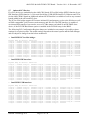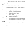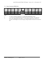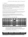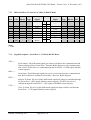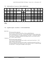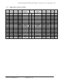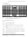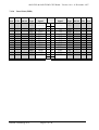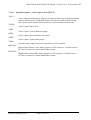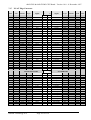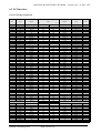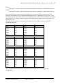
1
User’s Manual 686LCD/S & 686LCD/MG CPU Board Ver. 1.4.0 - 8. December 1997 INSIDE Technology A/S. 686LCD/S & 686LCD/MG CPU Board - Version 1.4.0 - 8. December 1997 Copyright Notice : Copyright 1996, INSIDE Technology A/S, ALL RIGHTS RESERVED. No part of this document may be reproduced or transmitted in any form or by any means, electronic or mechanical, for any purpose, with out the express written permission of INSIDE Technology A/S. Trademark Acknowledgement : Brand and product names are trademarks or registered trademarks of their respective owners. Disclaimer : INSIDE Technology A/S reserves the right to make changes, without notice, to any product, including circuits and/or software described or contained in this manual in order to improve design and/or performance. INSIDE Technology assumes no responsibility or liability for the use of the described product(s), conveys no license or title under any patent, copyright, or mask work rights to these products, and makes no representations or warranties that these products are free from patent, copyright, or mask work right infringement, unless otherwise specified. Applications that are described in this manual are for illustration purposes only. INSIDE Technology A/S makes no representation or warranty that such application will be suitable for the specified use without further testing or modification. Life Support Policy INSIDE Technology’s PRODUCTS ARE NOT FOR USE AS CRITICAL COMPONENTS IN LIFE SUPPORT DEVICES OR SYSTEMS WITHOUT EXPRESS WRITTEN APPROVAL OF THE GENERAL MANAGER OF INSIDE Technology A/S. As used herein : 1. Life support devices or systems are devices or systems which, (a) are intended for surgical implant into body, or (b) support or sustain life and whose failure to perform, when properly used in accordance with instructions for use provided in the labelling, can be reasonably expected to result in significant injury to the user. 2. A critical component is any component of a life support device or system whose failure to perform can be reasonably expected to cause the failure of the life support device or system, or to affect its safety or effectiveness. INSIDE Technology A/S. 686LCD/S & 686LCD/MG CPU Board - Version 1.4.0 - 8. December 1997 1. INTRODUCTION. ..........................................................................................................1 2. SYSTEM SPECIFICATION - SHORT FORM. ...............................................................2 2.1 System specification - Main data. ....................................................................................... 3 3. INSTALLATION PROCEDURE. ....................................................................................5 4. AMIBIOS SETUP...........................................................................................................6 4.1 AMIBIOS Setup Main Menu .............................................................................................. 7 4.1.1 Default Settings ............................................................................................................... 7 4.2 Setup Types........................................................................................................................... 8 4.2.1 Standard Setup................................................................................................................. 8 4.2.2 Advanced Setup ............................................................................................................. 11 4.2.3 Chipset Setup................................................................................................................. 14 4.2.4 Power Management Setup ............................................................................................. 16 4.2.5 PCI/PnP Setup ............................................................................................................... 18 4.2.6 Peripheral Setup - Inside Utility ................................................................................... 20 4.3 Utilities................................................................................................................................. 25 4.3.1 Detect IDE ..................................................................................................................... 25 4.4 Security................................................................................................................................ 25 4.4.1 AMIBIOS Password Support......................................................................................... 25 4.4.2 Setting a Password......................................................................................................... 25 4.4.3 Changing a Password..................................................................................................... 25 4.4.4 Anti-Virus ...................................................................................................................... 26 4.5 Default ................................................................................................................................. 27 4.6 AMIBIOS Power-On Self Test.......................................................................................... 27 4.7 INSIDE Interrupts ............................................................................................................. 28 5. SYSTEM RESOURCES ..............................................................................................30 5.1.1 Architecture, Functions and External connections: ....................................................... 30 5.2 Memory Map ...................................................................................................................... 31 5.3 I/O - Map............................................................................................................................. 32 5.4 Interrupt Usage................................................................................................................... 46 5.5 DMA-channel Usage........................................................................................................... 47 5.6 PCI Resources.................................................................................................................... 48 5.6.1 PCI Configuration Space ............................................................................................... 48 5.6.2 Configuration Space Registers ...................................................................................... 48 INSIDE Technology A/S. 686LCD/S & 686LCD/MG CPU Board - Version 1.4.0 - 8. December 1997 5.7 Onboard PCI Devices......................................................................................................... 53 6. DRIVER INSTALLATION. ...........................................................................................55 6.1 Driver installation for Ethernet Adapter ......................................................................... 55 6.1.1 Windows 95................................................................................................................... 55 6.1.2 Windows NT 4.0 Ethernet installation .......................................................................... 57 6.1.3 Windows for workgroups 3.11 ...................................................................................... 59 6.1.4 Driver options ................................................................................................................ 62 6.2 Driver installation for Display Adapter ........................................................................... 64 6.2.1 Windows 95................................................................................................................... 64 6.2.2 Windows NT 4.0 Display installation ........................................................................... 67 6.2.3 Windows 3.1X ............................................................................................................... 70 7. CONNECTOR DEFINITIONS. .....................................................................................72 7.1 Connector layout on Half Size PCB.................................................................................. 72 7.2 Symbol Descriptions........................................................................................................... 73 7.3 Keyboard Connectors. ....................................................................................................... 74 7.3.1 Pin-row Keyboard Connector (JPKBD). ....................................................................... 74 7.3.2 MINI-DIN Keyboard Connector (KBD)........................................................................ 74 7.3.3 Signal Description - Keyboard Connectors. .................................................................. 74 7.4 PS/2 Mouse Connector (JPMSE). ..................................................................................... 75 7.4.1 Signal Description - PS/2 Mouse................................................................................... 75 7.5 USB Connector (USBCON)............................................................................................... 76 7.5.1 Signal Description - USB Connector (USBCON)......................................................... 76 7.6 Power Connector (PWRCON). ......................................................................................... 77 7.7 Serial Port 1. ....................................................................................................................... 78 7.7.1 DB9 Serial Port 1 Connector (COM1) in RS232 Mode. ............................................... 78 7.7.2 Signal Description - Serial Port 1 - COM1 in RS232 Mode. ........................................ 79 7.7.3 DB9 Serial Port 1 Connector (COM1) in RS422 Mode. ............................................... 80 7.7.4 Signal Description - Serial Port 1 - COM1 in RS422 Mode. ........................................ 80 7.7.5 DB9 Serial Port 1 Connector (COM1) in RS485 Mode. ............................................... 81 7.7.6 Signal Description - Serial Port 1 - COM1 in RS485 Mode. ........................................ 81 7.8 Pin Header Serial Port 2 Connector (JPCOM2). ............................................................ 82 7.8.1 Serial Port 2 with external DB9 Connector. .................................................................. 82 7.8.2 Signal Description - Serial Port 2. ................................................................................. 83 7.9 Feature Connector (JPFEAT). .......................................................................................... 84 7.9.1 Signal Description - Feature Connector......................................................................... 85 7.10 Printer Port Connectors..................................................................................................... 86 7.10.1 Pin Header Printer Port Connector (JPLPT).................................................................. 86 7.10.2 DB25 Printer Port Connector......................................................................................... 87 7.10.3 Signal Description - Printer Port.................................................................................... 88 INSIDE Technology A/S. 686LCD/S & 686LCD/MG CPU Board - Version 1.4.0 - 8. December 1997 7.11 Floppy Disk Connector (JFLP). ........................................................................................ 89 7.11.1 Signal Description - Floppy Disk Connector................................................................. 90 7.12 IDE Hard Disk Connector (JIDE). ................................................................................... 91 7.12.1 Signal Description - IDE Hard Disk Connector. ........................................................... 92 7.13 Video Connectors. .............................................................................................................. 93 7.13.1 CRT Connector (CRT). ................................................................................................. 93 7.13.2 Signal Description - CRT Connector............................................................................. 93 7.13.3 Flat Panel Connector (JPLCD). ..................................................................................... 94 7.13.4 Signal Description - Flat Panel Connector. ................................................................... 95 7.13.5 Signal Configuration - Flat Panel Displays. .................................................................. 96 7.13.6 Panel Link (FPDI).......................................................................................................... 97 7.13.7 Signal Description - Panel Link (FPDI)......................................................................... 98 7.13.8 Flat Panel Utility Connector (LCDADP)....................................................................... 99 7.13.9 Signal Description - Flat Panel Utility Connector (LCDADP) ..................................... 99 7.13.10 Video Capture Port (JPYUV)................................................................................... 100 7.13.11 Signal Description - Video Capture Port (JPYUV).................................................. 101 7.14 Ethernet connector (10BASE)......................................................................................... 102 7.14.1 Signal Description - Ethernet connector (10BASE). ................................................... 102 7.15 AUI Connector (JPAUI). ................................................................................................. 103 7.15.1 Signal Description - AUI Connector (JPAUI). ............................................................ 103 7.16 PC104 Connector (PC104XT & PC104AT). .................................................................. 104 7.17 PC-AT Edge Connector. .................................................................................................. 105 7.17.1 Signal Description - PC-AT / PC104 Bus. .................................................................. 106 8. MAIN 686 COMPONENTS ........................................................................................110 9. MEASUREMENT DRAWING (686LCD/S).................................................................111 APPENDIX A : BIOS REVISIONS...................................................................................112 APPENDIX B: 686LCD/MG CPU Board.........................................................................113 INSIDE Technology A/S. 686LCD/S & 686LCD/MG CPU Board - Version 1.4.0 - 8. December 1997 Document revision history. Revision Date 1.0.0 July. 95. 1.0.1 1.1.0 1.2.0 1.3.0 1.4.0 By Comment KEA/CMU First preliminary version of manual created for the 686LCD/S Board. The manual contains preliminary connector signal descriptions. 12. Dec. 96. SJA Revised preliminary version. Connector signal descriptions revised. Specifications and Drawings updated. Installation procedure added. 29. Jan. 97 PJA/SST Revised preliminary version. BIOS setup added. Driver installation for Ethernet and VGA controller added. 14. Mar. 97 LJO Ethernet installation and Display installation for Windows NT 4.0 added. 2. Jul. 97 LJO/PJA Addition about 686LCD/MG added. 686LCD/S part corrected. 8. Dec. 97 PJA/JLA BIOS Setup updated. Resource map added. INSIDE Technology A/S. 686LCD/S & 686LCD/MG CPU Board - Version 1.4.0 - 8. December 1997 1. Introduction. This manual describes the 686LCD/S CPU Board made by INSIDE Technology A/S. Use of the manual implies a basic knowledge of PC-AT hard- and software. This manual is focused on describing the 686LCD/S CPU Board’s special features and is not intended to be a standard PCAT textbook. New users are recommended to study the short installation procedure stated in chapter 3. before switching-on the power. All configuration and setup of the CPU board is either done automatically or by the user in the CMOS setup menus - “no fight with several jumpers will be necessary”. INSIDE Technology A/S. Page 1 of 134 686LCD/S & 686LCD/MG CPU Board - Version 1.4.0 - 8. December 1997 2. System specification - short form. The 686LCD/S is a new standard for half size PENTIUM Computing Power. The 686LCD/S CPU Board is a fully featured PENTIUM computer implemented on a half size PC-AT-slot board. It can be used in commercial and industrial environments, especially in applications where very compact mechanical construction and low power consumption are required. It contains all the necessary functional modules, like CPU, DRAM-memory, video controller, Ethernet and peripheral interfaces on a single board, to implement a PENTIUM stand-alone computer system. The 686LCD/S is designed for maximum flexibility. It can be equipped with different PENTIUM Processors and memory components and several configuration parameters are freely re-programmable. A versatile 64 Bit on-board Video Controller with 2 MB Video Ram, supports a large number of different Flat Panel interfaces as well as standard VGA analogue monitors. For Flat Panel interface LVDS (Low Voltage Differential Signal) is implemented via PanelLink. Multimedia interface with YUV connector for direct Video input is also available. The 686LCD/S has two RS232C or 1 x RS232C and 1 x RS422/485 serial interface channels, one parallel printer port, one EIDE compatible hard disk interface and one floppy disk controller for peripheral support. The 686LCD/S include PCI Ethernet with 10BASE-T and “AUI” interface. USB (Universal Serial Bus) and IrDA-interface are implemented directly on the board. The 686LCD/S is equipped with a keyboard port, that supports standard AT compatible keyboards and a separate port for connection of a PS/2 mouse. For single board applications an optional Solid State Disk (SSD) with up to 8MB is available on board. The system can boot from Flash and is configured to behave just like any standard hard disk or floppy disk. A programmable watchdog timer and the power supply supervisor complement the standard board features to allow the use of the 686LCD/S in critical industrial environments. Processor temperature and fan supervision circuit is included. Onboard 3.3 Volt programmable switch mode power supply. Mixed voltage design with 3.3 volt Chipset, VGA, and PanelLink controller. The CMOS memory, containing the system parameters and date/time values, is backed up by an onboard Li battery. Permanent selected system parameters may alternatively be secured in the BIOS Flash. The 686LCD/S is equipped with a standard AMI System BIOS, a customised C&T VGA BIOS and INSIDE Technology's BIOS handling system set-up / configuration and solid state disk support. Additional controllers and/or user specific I/O-extension adapters may be added to the 686LCD/S CPU via the standard passive PC-AT backplane or the PC-104 connector. INSIDE Technology A/S. Page 2 of 134 686LCD/S & 686LCD/MG CPU Board - Version 1.4.0 - 8. December 1997 2.1 System specification - Main data. Processor INTEL, PENTIUM 75-233MHz, MMX. AMD, K6 166MHz-233MHz. AMD, K5 75-166MHz. System management mode is supported. CPU Clock Rate 75 - 233 MHz. System Clock Rate Processor/PCI : 66/33, 60/30, 50/25 MHz. Cache Memory Internal 16 kB (with Intel). External COAST 3.0 Module with 256 kB or 512 kB Pipelined Burst SRAM. Program Memory Up to 256MB DRAM memory, EDO or Fast Page. Up to 512MB DRAM on 686LCD/MG Boards. System Core INTEL 430HX, TRITON II Plug and Play Features All configuration is done by software (Automatic or usersetup). Automatic processor type detection and setup. Automatic remapping of on-board peripherals, if conflicts with off-board controllers are detected. Video Controller 64 Bit SVGA controller connected to PCI bus for fast access. Controls CRT monitors and Flat panel. Video Resolution 1280 x 1024 pixel (256 colors), SXGA. 1024 x 768 pixel (64 k colors), XGA. 800 x 600 pixel (16Mil. colors), SVGA. 640 x 480 pixel (16Mil. colors), VGA. Video Memory 2MB. Flat Panel Interface Plasma or EL, SS, 8 bit. Monochrome LCD, SS or DD, 8/16 bit. Passive colour STN LCD, SS or DD, 8/16/24 bit. Active colour TFT, SS, 9/12/15/16/18/24 bit. PanelLink PanelLink 65 MHz. 650 Mbit/sec. 3.3 Volt. Twisted pair IEEE-1284 Cable. (up to 10 m. distance to LCD) Ethernet 10M bit 10BASE-T and “AUI”. Controller on PCI bus with master access capabilities. USB Universal Serial Bus. 12 Mbit. INSIDE Technology A/S. Page 3 of 134 686LCD/S & 686LCD/MG CPU Board - Version 1.4.0 - 8. December 1997 Solid State Disk (SSD) Flash. Supports DIP32 Flash or SSD module with up to 8M byte Software driver handles SSD as normal hard disk drive. BIOS - System: American Megatrends, Industry standard, 128kB. - Video: Chips & Technologies, 44kB. - INSIDE BIOS extens.: Setup utility & SSD code, 64kB. - SCSI BIOS-extension: Adaptec SCSI Select, 24kB. (686LCD/MG only) Watchdog circuit Supervision of power supply and program execution. Startup delay. Service interval can be selected. Real-Time-Clock and CMOS Memory Date, time and system config. (with battery backup). Secure CMOS option Security backup of CMOS memory within Flash BIOS for auto reload, if CMOS memory is lost. Battery Circuit Exchangeable Li battery. CAUTION ! Danger of explosion if battery is incorrectly replaced. Replace only with the same or equivalent type recommended by the manufacturer. Dispose of used batteries according to the manufacturer’s instructions. Note: The battery is protected against internal and external shorting. On-board Peripheral interfaces AT-keyboard interface, PS/2 mouse interface, 2 x RS232C or 1 x RS232C & 1 x RS/485 serial communication interface supported by NS16550 comp. UART’s. 1 x Parallel printer interface (Centronic, ECP, EPP mode). EIDE hard disk interface Floppy drive interface (2 x 360kB to 1.44MB) Standard VGA Controller with Flat Panel Port. On-board protection All Peripheral interfaces intended for connection to external equipment are protected with EMI Suppression filters. System Bus Connectors 98 pin PC-AT bus edge connector. PC104-connector. On board Bus PCI for Ethernet, VGA, EIDE etc. Power Supply +5, +12 Volt (+/- 3%). Can operate at +5 volt only +3.6 Volt Battery (Lithium) 10-20W typical (Dependent on processor type) Power Consumption Environmental Conditions 0°C - 60°C operating temperature (forced cooling) 10% - 90% relative humidity (non-condensing) Dimensions 190.9 mm x 122.9 mm x 20.0-35.0 mm (686LCD/S) 249.7 mm x 122.9 mm x 20.0-35.0 mm (686LCD/MG) INSIDE Technology A/S. Page 4 of 134 686LCD/S & 686LCD/MG CPU Board - Version 1.4.0 - 8. December 1997 3. Installation procedure. 1. Turn off the power supply. 2. Insert the system BIOS if not already installed. Socket pin 1 is located nearest to the Cache socket. The chip must be placed so eventually unconnected socket pins are nearest the Cache socket. 3. Insert the DRAM (be careful with the orientation). 4. Insert Cache Module if applicable. 5. Install the processor (be careful with the orientation), pin 1 closest to the center of the Cache socket. 6. Mount the Fan on the top of the processor and connect it to JPFAN connector. 7. Remove the battery protection strip. 8. Insert all external cables for hard disk, floppy, keyboard etc. except for flat panel. A CRT monitor must be connected in order to change CMOS settings to flat panel support. 9. Connect power supply to the CPU Card via the PWRCON. 10. Turn on the power. 11. Enter the BIOS setup by pressing the delete key during boot up. Use the “Load BIOS Optimal Defaults” feature. The Peripheral Setup and the Standard Setup Window must be entered and configured correctly to match the particular system configuration. 12. If Flat Panel Display is to be utilised, make sure the Panel voltage in the BIOS setup is correct before turning off the power and connecting the display cable and optionally the FPUM. Note: The CMOS memory may be in a undefined state at power-on after a period of no battery backup. To load the fail-safe CMOS settings press and hold down the <<Esc>> key during power-up. INSIDE Technology A/S. Page 5 of 134 686LCD/S & 686LCD/MG CPU Board - Version 1.4.0 - 8. December 1997 4. AMIBIOS Setup. AMIBIOS Setup configures system information that is stored in CMOS RAM. AMIBIOS Setup has an easy-to-use graphical user interface that will be immediately recognisable to anyone who has ever used Microsoft Windows. This AMIBIOS Setup sets a new standard in BIOS user interfaces. The Main Setup Screen of the system BIOS is entered by pressing the <del> key during the start-up sequence when the following appears: Hit <DEL> if you want to run SETUP The AMIBIOS Setup can be accessed via keyboard, mouse, or pen. Help Screens AMIBIOS Setup provides Help Screens for Advanced Setup, Chipset Setup, Power Management Setup, and Peripheral Setup. Help on mouse and keyboard are also available. Choose Help by pressing <Alt> <H>. Using a Mouse with AMIBIOS Setup Point and Click Interface AMIBIOS Setup uses the familiar point and click navigation technique. The end user can point with the mouse anywhere on the screen, click the left mouse button, and AMIBIOS Setup control is transferred to the new location. The mouse click functions are: • single click to change or select both global and current fields and • double-click to perform an operation in the selected field. Using the Keyboard with AMIBIOS Setup AMIBIOS Setup has a built-in keyboard driver that uses simple keystroke combinations: Keystroke <Tab> →↓←↑ <Enter> + <Esc> <PgUp> <PgDn> <Home> <End> <Alt> <H> <Alt> <Spacebar> Alphabetic keys Numeric keys Function Move to the next window or field. Move to the next field to the right, below, left, or above. Select in the current field. Increments a value. Decrements a value. Closes the current operation and return to previous level. Returns to the previous page. Advances to the next page. Returns to the beginning of the text. Advances to the end of the text. Access a help window. Exit AMIBIOS Setup. A to Z are used in the Virtual Keyboard, and are not case-sensitive. 0 to 9 are used in the Virtual Keyboard and Numeric Keypad. Automatic AMIBIOS Setup Option Selection If selecting a certain setting for a specific AMIBIOS Setup option that determines the settings for one or more other AMIBIOS Setup options, AMIBIOS automatically assigns the dependent settings and does not permit the end user to modify these settings unless the setting for the parent option is changed. INSIDE Technology A/S. Page 6 of 134 686LCD/S & 686LCD/MG CPU Board - Version 1.4.0 - 8. December 1997 For example, the Serial Port options in Peripheral Setup can be set to 2F8h, 3F8h, 2E8h, or 3E8h. If 2F8h is chosen by the end user for Serial Port 1, AMIBIOS disables 2F8h for Serial Port 2. Invalid options are greyed and cannot be selected. 4.1 AMIBIOS Setup Main Menu The AMIBIOS Setup main menu is organised into four windows. Each window corresponds to a section in this chapter. Each section contains several icons. Clicking on each icon activates a specific function. The AMIBIOS Setup icons and functions are described in this chapter. The sections are: Windows Setup Utilities Security Default 4.1.1 Function The setup window has six icons that permit you to set system configuration options such as date, time, hard disk type, floppy disk type, and many others. The utility window has one icon that performs system functions. The security window has three icons that control AMIBIOS security features. The default window has three icons that permit you to select a group of settings for all AMIBIOS Setup options. Default Settings Each AMIBIOS Setup Option has two default settings. These settings can be applied to all AMIBIOS Setup Options when you select the Default window on the AMIBIOS Setup main menu. The types of defaults are: Optimal: These settings provide the optimal performance characteristics. Fail-Safe: The Power-On default settings consist of the most basic set of parameters. They are to be used as a reference in case the system is behaving erratically. They should always work, but do not provide optimal system performance characteristics. The system BIOS automatically loads these values, if the system parameters in the CMOS Memory is lost (ex. after shipping the CPU board with disconnected battery). INSIDE Technology A/S. Page 7 of 134 686LCD/S & 686LCD/MG CPU Board - Version 1.4.0 - 8. December 1997 4.2 Setup Types AMIBIOS Setup have six separate windows. Different types of system configuration parameters are set on each window. Type Standard Setup Advanced Setup Chipset Setup Power Management Setup PCI/PnP Setup INSIDE utilities 4.2.1 Description Set the time and date. Configure disk drives. Configure basic system performance parameters. Configure features specific to the onboard chipset. Configure power conservation features. Configure PCI and Plug-and-Play features. Configure I/O support. Standard Setup Standard Setup options are displayed by choosing the Standard icon from the AMIBIOS Setup menu. All Standard Setup options are described below. • Date/Time Select the Date/Time option to change the date or time. The current date and time are displayed. Enter new values through the displayed window. • Floppy Drive A, B Choose the Floppy Drive A or B icon to specify the floppy drive type. The settings are 360 KB 5¼”, 1.2 MB 5¼”, 720 KB 3½”, 1.44 MB 3½”, or 2.88 MB 3½”. • Pri Master • Pri Slave • Sec Master • Sec Slave Choose these icons to configure the hard disk drive named in the option. When you click on an icon, the following parameters are listed: Type, LBA/Large Mode, Block Mode, 32Bit Mode, and PIO Mode. All parameters relate to IDE drives except Type. Please note that Secondary Master and Slave Hard Disk drives are not supported in hardware and changing these settings will have no effect. Configuring a MFM Drive If configuring an old MFM hard disk drive, you must know the drive parameters (number of heads, number of cylinders, number of sectors, the starting write precompensation cylinder, and drive capacity). Choose Type and choose the appropriate hard disk drive type (1 - 46). The old MFM hard drive types are listed in table b. User-Defined Drive If you are configuring a SCSI drive or a MFM, RLL, ARLL, or ESDI drive with drive parameters that do not match drive types 1-46, you can select the User in the Type field. You must then enter the drive parameters as listed in table a on the window that appears. INSIDE Technology A/S. Page 8 of 134 686LCD/S & 686LCD/MG CPU Board - Version 1.4.0 - 8. December 1997 Table A Drive Parameters Parameter Type Cylinders Heads Write Precompensation Landing Zone Sectors Capacity Description The number for a drive with certain identification parameters. The number of cylinders in the disk drive. The number of heads. The size of a sector gets progressively smaller as the track diameter diminishes. Yet each sector must still hold 512 bytes. Write precompensation circuitry on the hard disk compensates for the physical difference in sector size by boosting the write current for sectors on inner tracks. This parameter is the track number where write precompensation begins. This number is the cylinder location where the heads will normally park when the system is shut down. The number of sectors per track. MFM drives have 17 sectors per track. RLL drives have 26 sectors per track. ESDI drives have 34 sectors per track. SCSI and IDE drives have more sectors per track. The formatted capacity of the drive is (Number of heads) x (Number of cylinders) x (Number of sectors per track) x (512 bytes per sector) Configuring IDE Drives If the hard disk drive to be configured as an IDE drive, select the appropriate drive icon (Pri Master, Pri Slave, Sec Master, or Sec Slave). By selecting Auto under types the IDE drive parameters are automatically detected (including ATAPI CD-ROM drives) and displayed. Click on the OK button to accept these parameters or you can set the parameters manually if you are absolutely certain that you know the correct IDE drive parameters. Click on LBA/Large Mode and choose On to enable support for IDE drives with capacities greater than 528 MB. Click on Block Mode and choose On to support IDE drives that use Block Mode. Click on 32Bit Mode and click on On to support IDE drives that permit 32-bit accesses. Click on PIO Mode to select the IDE Programmed I/O mode. PIO programming also works with ATAPI CD-ROM drives. The settings are Auto, 0, 1, 2, 3, 4, or 5. Click on Auto to allow AMIBIOS to automatically find the PIO mode that the IDE drive being configured uses. If you select 0-5 you must make absolutely certain that you are selecting the PIO mode supported by the IDE drive being configured. INSIDE Technology A/S. Page 9 of 134 686LCD/S & 686LCD/MG CPU Board - Version 1.4.0 - 8. December 1997 Hard Disk Drive Types Table B MFM types Type Cylinders Heads Write Precompensation Landing Zone Sectors Capacity 1 306 4 128 305 17 10 MB 2 615 4 300 615 17 20 MB 3 615 6 300 615 17 31 MB 4 940 8 512 940 17 62 MB 5 940 6 512 940 17 47 MB 6 615 4 65535 615 17 20 MB 7 462 8 256 511 17 31 MB 8 733 5 65535 733 17 30 MB 9 900 15 65535 901 17 112 MB 10 820 3 65535 820 17 20 MB 11 855 5 65535 855 17 35 MB 12 855 7 65535 855 17 50 MB 13 306 8 128 319 17 20 MB 14 733 7 65535 733 17 43 MB 16 612 4 0 663 17 20 MB 17 977 5 300 977 17 41 MB 18 977 7 65535 977 17 57 MB 19 1024 7 512 1023 17 60 MB 20 733 5 300 732 17 30 MB 21 733 7 300 732 17 43 MB 22 733 5 300 733 17 30 MB 23 306 4 0 336 17 10 MB 24 925 7 0 925 17 54 MB 25 925 9 65535 925 17 69 MB 26 754 7 754 754 17 44 MB 27 754 11 65535 754 17 69 MB 28 699 7 256 699 17 41 MB 29 823 10 65535 823 17 68 MB 53 MB 30 918 7 918 918 17 31 1024 11 65535 1024 17 94 MB 32 1024 15 65535 1024 17 128 MB 33 1024 5 1024 1024 17 43 MB 34 612 2 128 612 17 10 MB 35 1024 9 65535 1024 17 77 MB 36 1024 8 512 1024 17 68 MB 37 615 8 128 615 17 41 MB 38 987 3 987 987 17 25 MB 39 987 7 987 987 17 57 MB 40 820 6 820 820 17 41 MB 41 977 5 977 977 17 41 MB 42 981 5 981 981 17 41 MB 43 830 7 512 830 17 48 MB 44 830 10 65535 830 17 69 MB 45 917 15 65535 918 17 114 MB 46 1224 15 65535 1223 17 152 MB USER-DEFINED HARD DRIVE - Enter user-supplied parameters. INSIDE Technology A/S. Page 10 of 134 686LCD/S & 686LCD/MG CPU Board - Version 1.4.0 - 8. December 1997 4.2.2 Advanced Setup Advanced Setup options are displayed by choosing the Advanced icon from the AMIBIOS Setup main menu. All Advanced Setup options are described in this section. • Quick Boot Set this option to Enabled to instruct AMIBIOS to boot quickly when the computer is powered on. This option replaces the old Above 1 MB Memory Test Advanced Setup option. The settings are: Setting Disabled Enabled Description AMIBIOS test all system memory. AMIBIOS waits up to 40 seconds for a READY signal from the IDE hard disk drive. AMIBIOS waits for 0.5 second after sending a RESET signal to the IDE drive to allow the IDE drive time to get ready again. AMIBIOS checks for a <Del> key press and runs AMIBIOS Setup if the key has been pressed. AMIBIOS does not test system memory above 1 MB. AMIBIOS does not wait up to 40 seconds for a READY signal from the IDE hard disk drive. If a READY signal is not received immediately from the IDE drive, AMIBIOS does not configure that drive. AMIBIOS does not wait for 0.5 second after sending a RESET signal to the IDE drive to allow the IDE drive time to get ready again. AMIBIOS checks for a <Del> key press and runs AMIBIOS Setup if the key has been pressed. The Optimal setting is Enabled. The Fail-Safe setting is Disabled. • 1st Boot Device (flexboot) Selects the priority between the different boot devices. The options are IDE0-IDE3, Floppy, Floptical, Cdrom, SCSI, Network, or Disabled. Network boot supports the following networks: Novell server, IBM lan server, and Microsoft lan Manager server. The floptical drive is supported in BIOS as next available floppy drive and can be accessed through INT13 interface, using the assigned drive letter. BIOS can support maximum 2 floptical drives through the INT13 interface. The standard 1.44MB, 720KB, 120MB media and 1.2MB NEC format, 1.2MB Toshiba format, 1.7MB DMF format media can be used in the floptical drive. Note that 2.88MB media is not supported in floptical drive. The default setting is IDE-0. • 2nd Boot Device This device is the next boot device if the 1st boot device failed. The following options are available: IDE-0, Floppy, Floptical, Cdrom, and Disabled. The default setting is Floppy. • 3rd Boot Device Same as above with default setting to Cdrom. • Try other Boot Devices If set to Yes boot devices will be tried that was not selected in the 1st to 3rd boot device options. The default setting is Yes. • Display Mode at Add-On ROM Init The options are Forced BIOS and Keep Current. The selection of this setup question determines the display mode during add-on ROM (except Video add-on ROM) initialization. If selected as ‘Forced BIOS’, then before giving control to any add-on ROM, POST will force the display to be changed to BIOS mode. But if no add-on ROM is found, then the current display mode will remain unchanged even if this setup question is selected as ‘Forced BIOS’. If selected as ‘Keep Current’, then the current display mode will remain unchanged. INSIDE Technology A/S. Page 11 of 134 686LCD/S & 686LCD/MG CPU Board - Version 1.4.0 - 8. December 1997 • Floppy Access Control Setting this option to Read-only prevents the system to write to the floppy if the system uses the BIOS for disk access. Default is Read-Write. • Hard disk Access Control Setting this option to Read-only prevents the system to write to the hard drive if the system uses the BIOS for disk access. Default is Read-Write. • S.M.A.R.T for Hard disks (Self-Monitoring, Analysis and Reporting Technology) is a technology developed to manage the reliability of the hard disks by predicting some (but NOT ALL) of the future device failures. This feature helps BIOS warn the user of the possible device failure thereby giving user a chance to back up the device and replace the device before actual failure happens. S.M.A.R.T. capable devices should predict an impending failure and return that information through the Return S.M.A.R.T. Status command. Note that S.M.A.R.T. can not predict all future device failures and it should be used as an warning tool, not as a tool to predict the device reliability. The settings are enabled or disabled. The default setting is Disabled. • Boot Up Num Lock Set this option to Off to turn the Num Lock key off when the computer is booted so you can use the arrow keys on both the numeric keypad and the keyboard. The settings are On or Off. The default settings are On. • PS/2 Mouse support Function Set this option to Enabled to specify that IRQ12 will be used for the mouse. The settings are Disabled or Enabled. This option should be Enabled to use a PS/2type mouse. The Optimal and Fail-Safe default settings are Enabled. • Primary Display This option specifies the type of display monitor and adapter in the computer. The settings are Absent, VGA/EGA, CGA40x25, CGA80x25, or Mono. The Optimal and Fail-Safe default settings are VGA/EGA. • Password Check This option enables password checking every time the computer is powered on or every time AMIBIOS Setup is executed. If Always is chosen, a user password prompt appears every time the computer is turned on. If Setup is chosen, the password prompt appears if AMIBIOS is executed. The Optimal and Power-On default is Setup. See setting a password before using this option. • Parity check Set this option to Enabled to enable parity check on DRAM. The default setting is Disabled. • Boot to OS/2 Set this option to Enabled to permit AMIBIOS to run with IBM OS/2. The settings are Enabled or Disabled. The default settings are Disabled. • Wait For ‘F1’ If Error AMIBIOS POST runs system diagnostic tests that can generate a message followed by: Press <F1> to continue If this option is set to Enabled, AMIBIOS waits for the end user to press <F1> before continuing. If this option is set to Disabled, AMIBIOS continues the boot process without waiting for <F1> to be pressed. The settings are Enabled or Disabled. The Optimal default and Fail-Safe default settings are Disabled. INSIDE Technology A/S. Page 12 of 134 686LCD/S & 686LCD/MG CPU Board - Version 1.4.0 - 8. December 1997 • Internal Cache This option specifies the caching algorithm used for L1 internal cache memory. The settings are: Setting Disabled WriteBack (default) Description L1 internal cache memory on the CPU cache memory is disabled. Use the write-back caching algorithm. • External Cache This option specifies the caching algorithm used for L2 secondary (external) cache memory. The settings are: Setting Disabled WriteBack WriteThru (default) Description L2 secondary cache memory is disabled. Use the write-back caching algorithm. Use the write-through caching algorithm. • C000,16K Shadow • CC00,16K Shadow • D000,16K Shadow • D400,16K Shadow • D800,16K Shadow These options control the location of the contents of the 16KB of ROM beginning at the specified memory location. If no adapter ROM is using the named ROM area, this area is made available to the local bus. The settings are: Setting Enabled Cached Disabled (default) Description The contents of the video ROM area are copied (shadowed) from ROM to RAM for faster program execution. The contents of the video ROM area are not only copied from ROM to RAM, the contents of the RAM area can be written to or read from cache memory. The video ROM is not copied to RAM. The contents of the video ROM cannot be read from or written to cache memory. INSIDE Technology A/S. Page 13 of 134 686LCD/S & 686LCD/MG CPU Board - Version 1.4.0 - 8. December 1997 4.2.3 Chipset Setup This Setup menu configures features specific to the utilised chipset. • USB Function Enable Set this option to enable the BIOS USB (Universal Serial Bus) functions. The settings are Enabled or Disabled. By disabling the USB the USB resources are freed for other purposes. The Optimal and Fail-Safe settings are Disabled. • USB Keyboard Support Set this option to Enabled to enable USB support for USB keyboards in AMIBIOS. The settings are Enabled or Disabled. The Optimal and Fail-Safe settings are Disabled. • USB Passive Release Enable Set this option to Enabled to enable passive release on the universal serial bus. The settings are Enabled or Disabled. The Optimal and Fail-Safe settings are Enabled. • Global Triton2 Enable Set this option to Enabled to permit AMIBIOS to automatically configure the global features of the Intel82439HX chipset to optimal values based on the CPU frequency. The settings are Enabled or Disabled. The Optimal and Fail-Safe default settings are Enabled. • Memory Hole Use this option to specify an area in memory that cannot be addressed on the ISA bus. The settings are Disabled, 512-640K, or 15-16MB. The default settings are Disabled. • 8-Bit I/O Recovery Time (SYSCLK) This option specifies the length of the delay (in SYSCLKs) inserted between consecutive 8-bit I/O operations. The settings are Disabled, 8, 1, 2, 3, 4, 5, 6 or 7. The Optimal and Fail-Safe default settings are 1. • 16-Bit I/O Recovery Time (SYSCLK) This option specifies the length of the delay (in SYSCLKs) inserted between consecutive 16-bit I/O operations. The settings are Disabled, 4, 1, 2, or 3. The Optimal and Fail-Safe default settings are 1. • DRAM Timings This option specifies the RAS Access Time parameter for the installed DRAM SIMMs. The settings are Manual, 60ns, or 70ns. The Optimal default setting is 70ns. The Fail-Safe default setting is 70ns. • Refresh Rate This option specifies the refresh rate frequency for the installed DRAM SIMMs. The settings are 50 MHz, 60 MHz, or 66 MHz. The Optimal and FailSafe default settings are 66 MHz. • Turbo Read LeadOff Set this option to Enabled to enable the turbo read leadoff feature. The settings are Enabled or Disabled. The Optimal and Fail-Safe default settings are Disabled. • Read Burst Timing This option specifies the access timings for DRAM system memory read operations. The settings are x222, x333, or x444. The Optimal and FailSafe default settings are x333. • Write Burst Timing This option specifies the access timings for DRAM system memory write operations. The settings are x222, x333, or x444. The Optimal and FailSafe default settings are x333. INSIDE Technology A/S. Page 14 of 134 686LCD/S & 686LCD/MG CPU Board - Version 1.4.0 - 8. December 1997 • Fast RAS to CAS Delay (Clocks) This option specifies the length of a delay inserted between the assertion of the RAS and CAS signals. The settings are 2 (clocks) or 3 (clocks). The Optimal and Fail-Safe default settings are 3. • LeadOff Timing This option sets the leadoff timings for system memory access. The settings are 6/5/3/4, 6/5/4/5, 7/6/3/4, or 7/6/4/5. The Optimal and Fail-Safe default settings are 7/6/3/4. • Turbo Read Pipelining Set this option to Enabled to enable turbo read pipelining. The settings are Enabled or Disabled. The Optimal and Fail-Safe default settings are Disabled. • Speculative LeadOff Set this option to Enabled to enable the speculative leadoff feature. The settings are Enabled or Disabled. The Optimal and Fail-Safe default settings are Disabled. • Turn-Around Insertion Set this option to Enabled to enable the turnaround insertion feature. The settings are Enabled or Disabled. The Optimal and Fail-Safe default settings are Disabled. • Memory Address Drive Strength This option specifies the current strength (in milliamps) for system memory. The settings are 8mA/8mA, 8mA /12mA, 12mA /8mA, or 12mA /12mA. The Optimal and Fail-Safe settings are 8mA/8mA. • Type F DMA Buffer Control 1 • Type F DMA Buffer Control 2 These options specify the DMA channel that uses Type F DMA buffer control. The settings are Disabled, Channel-0, Channel-1, Channel-2, Channel-3, Channel-5, Channel-6, or Channel-7. The Optimal and Fail-Safe settings are Disabled. • NA Disable (NAD) for Ext Cache Set this option to Enable the NAD instruction for L2 secondary (external) cache memory. The settings are Enabled or Disabled. The Optimal and FailSafe settings are Enabled. • Peer Concurrency Set this option to Enabled to enable PCI peer-to-peer concurrency. The settings are Enabled or Disabled. The Optimal and Fail-Safe settings are Enabled. • DRAM Data Integrity Mode This option can only be implemented when the system is populated with a 72-bit wide memory. The DRAM interface can either be ECC or Parity checked. If Parity is selected the DRAM parity protection is 8-bit based even parity. Selecting ECC will detect all single and dual-bit errors during DRAM reads. The corrected data is transferred to the requester and is not back written to DRAM. If not all DRAM modules are 72-bit wide, but some are 64-bit, it is important to disable all error checking by Disabling ECC Test and selecting the ECC DRAM Data Integrity Mode. The Default and Fail-Safe settings are Parity. • PCI 2.1 Passive Release Enable Set this option to Enabled to enable the PCI passive release feature defined in Version 2.1 of the PCI specifications. The settings are Enabled or Disabled. The Optimal and Fail-Safe settings are Enabled. • Delayed Transaction Enable Set this option to Enabled to enable delayed transactions. The settings are Enabled or Disabled. The Optimal and Fail-Safe settings are Enabled. • North Bridge Retry Enable Set this option to Enabled to enable North Bridge Retry. The Optimal and Fail-Safe settings are Enabled. INSIDE Technology A/S. Page 15 of 134 686LCD/S & 686LCD/MG CPU Board - Version 1.4.0 - 8. December 1997 4.2.4 Power Management Setup Power Management Setup options are displayed by choosing the Power Management icon from the AMIBIOS Setup main menu. All Power Management Setup options are described in this section. The Advanced Power Management specification defines four power states: Power State Affects…. Ready In the ready state the computer or device is fully powered up and ready for use. The computer can be active or idle. The Standby State is an intermediate system-dependent state that tries to conserve power. The state is entered when the CPU is idle for a pre-specified length of time. The computer does not return to the Ready state until a device raises a hardware interrupt or a device is accessed. All data and operational parameters are preserved. Suspend is the lowest level of power consumption available that still preserves operational data and parameters. When the computer is in Suspend mode, no computation is performed until normal activity is resumed. Activity cannot resume unless signalled by an external event. The computer is powered down and inactive in Off state. Data and operational parameters may or may not be preserved in this state. Standby Suspend Off • Power Management/APM Set this option to Enabled to enable the power management and APM (Advanced Power Management) features. The settings are Disabled, Enabled or Inst-on. Selecting the option Inst-on is not supported unless external hardware is added. The default Optimal setting is Enabled. The Fail-Safe setting is Disabled. • Instant-On Timeout This option specifies the length of a period of system inactivity while the computer is in Full power on state. When this length of time expires, AMIBIOS takes the computer to a lower power consumption state, but the computer can return to full power instantly when any system activity occurs. The settings are Disabled, 1 Min, 2 Min, and all one minute intervals up to and including 15 Min. The default settings are Disabled. • Green PC Monitor Power State This option specifies the power management state that the Green PC-compliant video monitor enters after the specified period of display inactivity has expired. The settings are Standby, Suspend or Off. The default settings are Standby. • Video Power Down Mode This option specifies the power management state that the video subsystem enters after the specified period of display inactivity has expired. The settings are Disabled, Standby, or Suspend. The default settings are Disabled. • Hard Disk Power Down Mode This option specifies the power management state that the hard disk drive enters after the specified period of display inactivity has expired. The settings are Disabled, Standby, or Suspend. The default settings are Disabled. • Hard Disk Time Out (Minutes) This option specifies the length of a period of hard disk drive inactivity. When this length of time expires, the computer enters power-conserving state specified in the Hard Disk Power Down Mode option. The settings are Disabled, 1 Min, 2 Min, and all one minute intervals up to and including 15 Min. The default settings are Disabled. INSIDE Technology A/S. Page 16 of 134 686LCD/S & 686LCD/MG CPU Board - Version 1.4.0 - 8. December 1997 • Standby Time Out (Minutes) This option specifies the length of the period of system inactivity when the computer is in Full-On mode before the computer is placed in Standby mode. In Standby mode, some power use is curtailed. The settings are Disabled, 1 Min, 2 Min, and all one minute intervals up to and including 15 Min. The default settings are Disabled. • Suspend Time Out (Minutes) This option specifies the length of the period of system inactivity when the computer is already in Standby mode before the computer is placed in Suspend mode. In Suspend mode, nearly all power use is curtailed. The settings are Disabled, 1 Min, 2 Min, and all one minute intervals up to and including 15 Min. The default settings are Disabled. • Slow Clock Ratio This option specifies the speed at which the system clock runs in power saving modes. The settings are expressed as a ratio between the normal clock speed and the power down clock speed. The settings are 1:1, 1:2 (half as fast as specified in Peripheral Setup), 1:4, 1:8, 1:16, 1:32, 1:64, or 1:128. The default settings are 1:8. • Display Activity This option specifies if AMIBIOS is to monitor activity on the display monitor for power conservation purposes. When this options is set to Monitor and there is no display activity for the length of time specified in the value in the Full-On to Standby Timeout (Min) option, the computer enters a power saving state. The settings are Monitor or Ignore. The default settings are Ignore. • IRQ3 • IRQ4 • IRQ5 • IRQ7 • IRQ9 • IRQ10 • IRQ11 • IRQ12 • IRQ13 • IRQ14 • IRQ15 When set to Monitor, these options enable event monitoring on the specified hardware interrupt request line. If set to Monitor and the computer is in a power saving mode, AMIBIOS watches for activity on the specified IRQ line. The computers enters the full on power state if any activity occurs. AMIBIOS reloads the Standby and Suspend timeout timers if activity occurs on the specified IRQ line. The settings for each of these options are Monitor or Ignore. The Fail-Safe default settings are all Ignore. The Optimal settings are all Ignore except on IRQ12 and IRQ14 which are Monitor. INSIDE Technology A/S. Page 17 of 134 686LCD/S & 686LCD/MG CPU Board - Version 1.4.0 - 8. December 1997 4.2.5 PCI/PnP Setup PCI/PnP Setup options are displayed by choosing the PCI/PnP Setup icon from the AMIBIOS Setup main menu. All PCI/PnP Setup options are described in this section. • Plug and Play Aware OS Set this option to Yes if the operating system installed in the computer is Plug and Play-aware. AMIBIOS only detects and enables PnP ISA adapter cards that are required for system boot. The Windows 95 operating system detects and enables all other PnPaware adapter cards. Windows 95 is PnP-aware. Set this option to No if the operating system (such as DOS, OS/2, Windows 3.x) does not use PnP. You must set this option correctly or PnP-aware adapter cards installed in your computer will not be configured properly. The settings are No or Yes. The Optimal and Fail-Safe default settings are No. • PCI Latency Timer (in PCI Clocks) This option sets latency of all PCI devices on the PCI bus. The settings are in units equal to PCI clocks. The settings are 32, 64, 96, 128, 160, 192, 224, or 248. The Optimal and Fail-Safe default settings are 64. • PCI VGA Palette Snoop This option must be set to Enabled if any ISA adapter card installed in the computer requires VGA palette snooping. When set to Enabled, multiple VGA devices operating on different buses can handle data from the CPU on each set of palette registers on every video device. The settings are Disabled or Enabled. The Optimal and Fail-Safe default settings are Disabled. • PCI IDE Bus Master Set this option to Enabled to specify that the IDE controller on the PCI local bus has bus mastering capability. The settings are Disabled or Enabled. The Optimal and FailSafe default settings are Disabled. • Off-board PCI IDE Card This option specifies if an off-board PCI IDE controller adapter card is used in the computer. You must also specify the PCI expansion slot on the motherboard where the off-board PCI IDE controller card is installed. If an off-board PCI IDE controller is used, the onboard IDE controller on the motherboard is automatically disabled. The settings are Auto, Slot1, Slot2, Slot3, Slot4, Slot5, or Slot6. If Auto is selected, AMIBIOS automatically determines the correct setting for this option. The Optimal and Fail-Safe default settings are Auto. In the AMIBIOS for the Intel Triton chipset, this option forces IRQ 14 and 15 to a PCI slot on the PCI local bus. This is necessary to support non-compliant PCI IDE adapter cards. If an off-board PCI IDE controller adapter card is installed in the computer, you must also set the options Off-board PCI IDE Primary and Secondary IRQ. • Off-board PCI IDE Primary IRQ This option specifies the PCI interrupt used by the primary IDE channel on the off-board PCI IDE controller. The settings are Disabled, INTA, INTB, INTC, INTD, or Hardwired. The Optimal and Fail-Safe default settings are Disabled. • Off-board PCI IDE Secondary IRQ This option specifies the PCI interrupt used by the secondary IDE channel on the off-board PCI IDE controller. The settings are Disabled, INTA, INTB, INTC, INTD or Hardwired. The Optimal and Fail-Safe default settings are Disabled. INSIDE Technology A/S. Page 18 of 134 686LCD/S & 686LCD/MG CPU Board - Version 1.4.0 - 8. December 1997 • DMA Channel 0 • DMA Channel 1 • DMA Channel 3 • DMA Channel 5 • DMA Channel 6 • DMA Channel 7 These options specify if the named DMA channel is available for use on the ISA/EISA bus or for PnP (Plug and Play). The settings are ISA/EISA or PnP. The Optimal and Fail-Safe default settings are PnP. • IRQ3 • IRQ4 • IRQ5 • IRQ7 • IRQ9 • IRQ10 • IRQ11 • IRQ14 • IRQ15 These options specify the bus that the named interrupt request lines (IRQs) are used on. These options allow you to specify IRQs for use by legacy ISA adapter cards. These options determine if AMIBIOS should remove an IRQ from the pool of available IRQs passed to BIOS configurable devices. The available IRQ pool is determined by reading the ESCD CMOS memory. If more IRQs must be removed from the pool, the end user can use these PCI/PnP Setup options to remove the IRQ by assigning the option to the ISA/EISA setting. Onboard I/O is configurable by AMIBIOS. The IRQs used by onboard I/O are configured as PCI/PnP. The settings are PCI/PnP or ISA/EISA. The Optimal and Fail-Safe default settings are PCI/PnP. • Reserved Memory Size This option specifies the size of the memory area reserved for legacy ISA adapter cards. The settings are Disabled, 16K, 32K, or 64K. The Optimal and Fail-Safe default settings are Disabled. • Reserved Memory Address This option specifies the beginning address (in hex) of the reserved memory area. The specified ROM memory area is reserved for use by legacy ISA adapter cards. The settings are C0000, C4000, C8000, CC000, D0000, D4000, D8000, or DC000. The Optimal and Fail-Safe default settings are C8000. Note that C0000h-CAFFFh are used by Video BIOS ROM and CB000h-D1FFFh by SCSI Bios Extension if enabled (on MG boards). INSIDE Technology A/S. Page 19 of 134 686LCD/S & 686LCD/MG CPU Board - Version 1.4.0 - 8. December 1997 4.2.6 Peripheral Setup - Inside Utility Peripheral Setup options are displayed by choosing the Peripheral Setup icon from the AMIBIOS Setup main menu. All Peripheral Setup options are described in this section. • Processor Clock (INT/EXT) This option should be set to the clock frequencies corresponding to the installed CPU. The options are 75/50, 90/60, 100/50, 100/66, 120/60, 133/66, 150/60, 166/66, or 200/66. The number before the slash is the Internal Processor Clock and the number after is the External Clock. The Optimal and Fail-Safe settings are 75/50. To activate a new selection the machine must be powered down. • Secure CMOS This feature gives the opportunity to save the contents of the CMOS in the flash, providing a failsafe system independent of the battery state (backup of CMOS memory). The default setting is Disabled. The CMOS will be stored in the flash when set to Activated and the setup is exit by : “Save changes and Exit”. • Ethernet Controller Here the Ethernet controller can be set On or Off. The default settings are On. By disabling the Ethernet controller the resources are freed. • SCSI Controller This option can enable or disable the SCSI controller, the settings are On or Off. This setting is only valid on 686LCD/MG boards and have no meaning on /S boards. By disabling the SCSI controller the resources are freed. • VGA Controller With this option the attached VGA device can be set to minimise the overall power consumption of the board, when only one VGA device is connected. By disabling the VGA controller the resources are freed. To use an off-board VGA controller, the on-board controller must be set to Off. The default settings are On. • Display Type The possible settings of the display type are CRT only, Panel only or CRT and Panel, with default settings: CRT only. Notice that a CRT device is needed to change the BIOS settings for flat panel use or when the CMOS settings are lost. Note that an erroneous choice can mean blank screen. • Panel Driver This option give the user a choice between 14 standard configured Chips & Technologies panels. Changing this setting will reset the Panel Interface setting to 3.3 V. The Default and Fail-Safe settings are 1024*768 STN. This interface is only present if the display data block is not uploaded to flash. Note that the display data block (in this case V1.00) can be updated independently of the other BIOS files. If display data block is present together with BIOS release 110.306.627 or newer the following menu will appear: INSIDE Technology A/S. Page 20 of 134 686LCD/S & 686LCD/MG CPU Board - Version 1.4.0 - 8. December 1997 Display module V1.00 [ ] [X] [ ] [ ] [ ] [ ] Resolution 320 X 240 640 X 480 800 X 600 854 X 480 1024 X 768 1280 X 1024 [ ] [ ] [ ] [ ] [ ] [X] [ ] Technology STN Mono EL Mono TFT Mono STN Color EL Color TFT Color Plasma Manufacturer [ ] Standard [X] [ ] Fujitsu [ ] IBM [ ] FPD [ ] Sharp [X] Goldstar [ ] Toshiba [ ] Hitachi [ ] Hosiden [ ] Kyocera [ ] NEC [ ] Optrex [ ] Planar [ ] Samsung [ ] Torisan Driver selection : 05h Code LCA4VE02A Selections can be made either by keyboard with the keys : ÇÈ,Tab + Enter or simply by clicking on the checkbox with the mouse. When the 3 criteria are selected : Resolution, Technology and Manufacturer, different “Codes” or “NON” will appear in the right side of the screen. Simply select the exact display code according to the display. The “driver selection” presented in bottom of the screen indicate the display number to lock with, if using the “BFLASH” utility. • Panel Interface By changing this setting the user can specify the Panel Interface voltage. The settings are 3.3 Volts or 5.0 Volts. The Default and Fail-Safe settings are 3.3 Volts. Warning : Always check the Panel specifications to make sure it can handle a higher voltage, before changing the default parameter. • JPLCD Pin 5 This feature is added to ease the connection to plasma displays which requires an inversion of the data clock signal : SHFCLK. The default setting is GPO2 where pin 5 on the LCD connector outputs the signal GPIO2. The other option is /SHFCLK. Selecting this option does not affect the original SFKCLK signal (pin 13). • SSD Drive This option sets up the Solid State Disk Drive. The options are Off, A, B, C, or Last DRV. If set to Off the Solid State Disk cannot be accessed. If set to A: the system will attempt to boot on the SSD if the 1st boot device in the Advanced setup is floppy. If a A: floppy drive exists it will be remapped to B:. If set to B: the SSD will be accessed through B: and will overrule any B: floppy drives present. If set to C: the system will attempt to boot on the SSD, and any harddisk present will be remapped to D:. This selection has to be chosen if preparation of a bootable SSD emulating drive C: is desired. If set to Last DRV the SSD will be assigned the last available drive designator. If for example a hard disk is attached as C:, the SSD will be assigned D:. INSIDE Technology A/S. Page 21 of 134 686LCD/S & 686LCD/MG CPU Board - Version 1.4.0 - 8. December 1997 The Optimal and Fail-Safe settings are Off. The Solid State Disk can be used as both A:, B:, C:, and Last DRV under DOS. To use the Disk under Windows 95 the disk must be set as C: or Last DRV. To use EMM handlers remember to exclude the E0000-segment, or the Solid State Disk may be inaccessible. The SSD drive is not supported under Windows NT. • SSD Prepare Option is used for preparing the Solid State Disk. The options are Off or Activated. If Activated the SSD will be low-level formatted at next boot-up and are hereafter automatically reset to Off. The Optimal and Fail-Safe settings are Off. • On-Board FDC This option enables the floppy drive controller on the motherboard. The settings are Auto, Enabled or Disabled. The Optimal and Fail-Safe default settings are Auto. • On-Board Serial Port 1 This option enables serial port 1 on the motherboard and specifies the base I/O port address for serial port 1. The settings are Auto, Disabled, 3F8h, 2F8h, 3E8h, or 2E8h. The Optimal default setting is 3F8h. The Fail-Safe default setting is Auto. • Serial Port 1 Interface This option is only available if the On-Board Serial Port 1 is not Disabled. The possible settings for the serial interface standard are Disabled, RS232, RS422, or RS485. Notice that the default settings are both Disabled, to prevent potential conflicts and damaging voltage levels when connecting serial devices before running AMIBIOS. Caution: Always check the serial device interface standard and this setting before connecting the device. • On-Board Serial Port 2 This option enables serial port 2 on the motherboard and specifies the base I/O port address for serial port 2. The settings are Auto, Disabled, 3F8h, 2F8h, 3E8h, or 2E8h. The Optimal and Fail-Safe default settings are Auto. • Serial Port 2 Mode This option is only available if the On-Board Serial Port 2 is not Disabled. The settings for the serial interface standard are Normal (RS232), IrDA SIR-A, ASK-IR, IrDA SIR-B, IrDA HDLC, IrDA 4PPM,Consumer, Raw IR. The default settings are Normal . IR Duplex mode Receiver polarity Transmitter polarity Normal* IrDA SIR-A N/A Full* N/A Half ASK-IR Full* Half IrDA SIR-B Full* Half IrDA HDLC Full* Half IrDA 4PPM Full* Half Consumer Full* Half Raw IR Full* Half N/A Active High* Active High* Active High* Active High* Active High* Active High* Active High* N/A Active High Active High Active High Active High Active High Active High Active High N/A Active Low Active Low Active Low Active Low Active Low Active Low Active Low Indicate default setting. INSIDE Technology A/S. Page 22 of 134 N/A Active Low* Active Low* Active Low* Active Low* Active Low* Active Low* Active Low* Fast IR port N/A N/A Fast IR DMA N/A N/A N/A N/A Auto N/A Auto Auto Auto Auto Auto Auto Auto Auto 686LCD/S & 686LCD/MG CPU Board - Version 1.4.0 - 8. December 1997 • On-Board Parallel Port This option enables the parallel port on the motherboard and specifies the parallel port base I/O port address. The settings are Auto, Disabled, 378h, 278h, or 3BCh. The Optimal and Fail-Safe default settings are Auto. • Parallel Port Mode This option specifies the parallel port mode. ECP and EPP are both bi-directional data transfer schemes that adhere to the IEEE P1284 specifications. The settings are: Setting Normal (default) EPP ECP Description The normal parallel port mode is used. The parallel port can be used with devices that adhere to the Enhanced Parallel Port (EPP) specification. EPP uses the existing parallel port signals to provide asymmetric bi-directional data transfer driven by the host device. The parallel port can be used with devices that adhere to the Extended Capabilities Port (ECP) specification. ECP uses the DMA protocol to achieve transfer rates of approximately 2.5 Mbs. ECP provides symmetric bi-directional communications. • EPP Version Sets the EPP version revision to either 1.9 or 1.7. The default settings are 1.9. This option is only valid if the Parallel Port Mode option is EPP. • Parallel Port IRQ This option sets the Parallel Port IRQ number and is only available if On-Board Parallel Port is not Auto or Disabled. The settings are 5 or 7 where IRQ7 is the default Optimal and Fail-Safe setting. • Parallel Port DMA Channel This option is only available if the setting for the Parallel Port Mode option is ECP and the On-Board Parallel Port option is not Auto or Disabled. The settings are DMA channel 0, 1, or 3. The default settings are 3. • On-Board Speaker Sets the speaker On or Off. Default settings are On. • General Purpose IO 0 (Will be occupied by FPUM if module is present) • General Purpose IO 1 • General Purpose IO 2 (Will be occupied by FPUM if module is present) • General Purpose IO 3 (Will be occupied by FPUM if module is present) • General Purpose IO 4 (Can also be setup to indicate Low temp.) • General Purpose IO 5 (Can also be setup to indicate High temp.) • General Purpose IO 6 (Can also be setup to indicate Low current.) • General Purpose IO 7 (Can also be setup to indicate High current.) Each GP IO can be setup to one of the following: Input, Output(low), or Output(high). Default setting is Input. If Output is selected the value in (x) indicate the startup state. GP IO 4-7 also have an additional option, this can be used to control the environment or indicate alarms with LED etc. Low temp and Low current are determined by hardware and can not be changed. • Watch Dog Timeout Action By setting this option to Reset a hardware supervision of the software is activated and the software will need to “service” the watchdog in order to avoid system reset. When active the software must “service” within 1.5 minute after power-on, and then within the period set up in the next option. The “service” is executed by dummy writing to 2 I/O addresses subsequently, namely F0h and F3h. INSIDE Technology A/S. Page 23 of 134 686LCD/S & 686LCD/MG CPU Board - Version 1.4.0 - 8. December 1997 • Watch Dog Timeout Periods Only valid if above selection is set to Reset. The following set up the allowed time between the each “service” : 0.2, 0.8, 1.2, 1.6, 2.0, 2.4 or 2.8 seconds. • Inside Interrupt This option specifies a software interrupt that can be used for backlight and contrast control for flat panels presently, it can also access the GP IO’s. Special drivers are needed for this purpose. The options are 45h, 47h, 48h, 49h, 65h, 66h, 68h or Off. Select Off to disable Inside Interrupt. (See chapter ?? for usage) • High Temperature Limit From PCB revision 20100192 (686LCD/MG boards) and revision 20100164 (686LCD/S boards) a temperature monitoring circuit is included on-board. The actual temperature close to the CPU is displayed in the Actual field in the BIOS setup. The maximum limit for this temperature can be set by clicking on the right field. The Low temperature limit is predefined to be <5C° and will also cause a violation. The desired action is chosen in the next option. When this limit is exceeded GPIO 5 can be setup to be high. • Temperature Violation Action This option gives the user three choices for actions to be taken when the high temperature limit is reached as set in the previous option. The choices are Nothing, Speaker, and CPU-speed. The default settings are Nothing. If Speaker is selected the speaker will beep if a violation is detected. If CPU-speed is selected the CPU is clocked down. • High Current Limit From PCB revision 20100192 (686LCD/MG boards) and revision 20100164 (686LCD/S boards) a current measuring circuit is included on-board that measures the actual current to the fan (supplied through the JPFAN connector). The actual current is displayed in the Actual field in the BIOS setup. The maximum limit for this current can be set by clicking on the right field. The Low current limit is predefined to be <10mA and will also cause a violation. The desired action is chosen in the next option. When this limit is exceeded GPIO 7 can be setup to be high. • Current Violation Action This option gives the user two choices for actions to be taken when the high current limit is reached as set in the previous option. The choices are Nothing and Speaker. The default settings are Nothing. If Speaker is selected the speaker will beep if a violation is detected. Hint: When making the adjustment for the high limits do not set the limit close to the normal operating temperature. The trimming is aided by up and down arrows next to the measured value. • On-Board IDE This option specifies the channel used by the IDE controller on the motherboard. The settings are Disabled, Primary, Secondary, or Both with default settings as Primary. INSIDE Technology A/S. Page 24 of 134 686LCD/S & 686LCD/MG CPU Board - Version 1.4.0 - 8. December 1997 4.3 Utilities The following icons appear in this section of the AMIBIOS main screen. 4.3.1 Detect IDE 4.4 Security Three icons appear in this part of the AMIBIOS Setup screen: • Supervisor (Password), • User (Password), and • Anti-Virus. Two Levels of Passwords Both the Supervisor and the User icons configure password support. If you use both, the Supervisor password must be set first. The system can be configured so that all users must enter a password every time the system boots or when AMIBIOS Setup is executed, using either or both the Supervisor password or User password. 4.4.1 AMIBIOS Password Support The Supervisor and User icons activate two different levels of password security. If AMIBIOS Setup has an optional password feature. The system can be configured so that all users must enter a password every time the system boots or when AMIBIOS Setup is executed. 4.4.2 Setting a Password The password check option is enabled in Advanced Setup by choosing either Always (the password prompt appears every time the system is powered on) or Setup (the password prompt appears only when AMIBIOS is run). The password is encrypted and stored in CMOS memory. You are prompted for a 1 – 6 character password. You can either type the password on the keyboard or select each letter of the password, one at a time, using the mouse. The password does not appear on the screen when typed. Make sure you write it down. If you forget it, you must drain CMOS memory and reconfigure. If You Do Not Want to Use a Password Press <Enter> when the password prompt appears. 4.4.3 Changing a Password Select the Supervisor or User icon from the Security section of the AMIBIOS Setup main menu. Enter the password and press <Enter>. The screen does not display the characters entered. After the new password is entered, retype the new password as prompted and press <Enter>. If the password confirmation is incorrect, an error message appears. If the new password is entered without error, press <Esc>. The password is stored in CMOS memory after AMIBIOS completes. The next time the system boots, a password prompt appears if the password function is present and enabled. Remember the Password Keep a record of the new password when the password is changed. If you forget the password, you must erase the system configuration information in CMOS memory. This can be done by pressing <Del> during boot or taking the battery out for 5 minutes. INSIDE Technology A/S. Page 25 of 134 686LCD/S & 686LCD/MG CPU Board - Version 1.4.0 - 8. December 1997 4.4.4 Anti-Virus When this icon is selected from the Security section of the AMIBIOS Setup main menu, AMIBIOS issues a warning when any program (or virus) issues a Disk Format command or attempts to write to the boot sector of the hard disk drive. The settings are Enabled or Disabled. If enabled, the following appears when a write is attempted to the boot sector. You may have to type N several times to prevent the boot sector write. Boot Sector Write!!! Possible VIRUS: Continue (Y/N)? _ The following appears after any attempt to format any cylinder, head, or sector of any hard disk drive via the BIOS INT 13 Hard Disk Drive Service: Format!!! Possible VIRUS: Continue (Y/N)? _ INSIDE Technology A/S. Page 26 of 134 686LCD/S & 686LCD/MG CPU Board - Version 1.4.0 - 8. December 1997 4.5 Default The icons in this section permit you to select a group of settings for all AMIBIOS Setup options. Not only can you use these icons to quickly set system configuration parameters, you can choose a group of settings that have a better chance of working when the system is having configurationrelated problems. • Original Choose the Original icon to return to the system configuration values present in AMIBIOS Setup when you first began this AMIBIOS Setup session. • Optimal You can load the optimal default settings for the AMIBIOS by selecting the Optimal icon. The Optimal default settings are best-case values that should optimise system performance. If CMOS memory is corrupted, the Optimal settings are loaded automatically. • Fail-Safe You can load the Fail-Safe AMIBIOS Setup option settings by selecting the Fail-Safe icon from the Default section of the AMIBIOS Setup main menu. The Fail-Safe settings provide far from optimal system performance, but are the most stable settings. Use this option as a diagnostic aid if the system is behaving erratically. 4.6 AMIBIOS Power-On Self Test Every time the system is powered on, AMIBIOS executes a power-on self test. In case of errors they are reported in one of two ways. If the error occurs before the display device is initialised, a series of beeps sound. Beep codes indicate that a fatal error has occurred. AMIBIOS Beep Codes are described in the table below. If it beeps… Then… 1, 2, or 3 times Re-insert the memory SIMMs. If the system still beeps replace the memory. Try a different keyboard or replace the keyboard fuse if the keyboard has one. There is an error on the Video adapter or the Video RAM The BIOS ROM chip is bad. The system probably needs a new BIOS ROM chip. Re-insert the cache memory on the board. If it still beeps, replace the cache memory. Fatal error. 6 times 8 times 9 times 11 times 4, 5, 7, or 10 times If the error occurs after the display device is initialised, an error message is displayed. INSIDE Technology A/S. Page 27 of 134 686LCD/S & 686LCD/MG CPU Board - Version 1.4.0 - 8. December 1997 4.7 INSIDE Interrupts The interrupt number is selected in the INSIDE Utilities setup menu. By loading the desired function number in the AL CPU register and generating a software interrupt with the INT X instruction the function is called. X is the interrupt number specified in the Inside utility setup. Some of the functions will require an additional value loaded in the AH register. The software interrupt is used to control the following: Function 00h, Diagnostic call. This call can be used to test whether the interrupt is setup correct. Input : AL = Output : AL = 00h 5Ah Function 10h, Enable displays. This call enables or disables the CRT and Flat panel outputs. Input : AL = AH = 10h 00h : Disable both CRT and Flat panel outputs. 01h : Enable CRT and disable Flat panel output. 02h : Disable CRT and enable Flat panel output. 03h : Enable both CRT and Flat panel outputs. Function 20h, Write to general purpose digital outputs. This function is used to access the general purpose pins GPIO7..0 in the JPFEAT connector. Input : AL = AH = 20h The port value to be written. GPIO0 in bit 0 of AH. Function 21h, Read back from general purpose digital outputs. This function is used to read back values directly on the GPIO pins. Input : AL = Output : AH = 21h The read port value. GPIO0 in bit 0 of AH. Function 22h, Same as function 21h for compatibility reasons. INSIDE Technology A/S. Page 28 of 134 686LCD/S & 686LCD/MG CPU Board - Version 1.4.0 - 8. December 1997 Function 23h, Setup GPIO’s This function allows the user to control the definitions on the GPIO pins, could be used in e.g. a multidrop application. The states are only changed dynamically, when booting next time the definition will be overwritten by the CMOS setup values. Input : AL = AH = 23h Port definition, GPIO0 in bit 0 of AH, where 1’s present an input state. Function 30h, Set the default display contrast. Sets the default contrast level for the connected LCD panel. This feature is useful only if the Flat Panel Utility Module (FPUM) is present. Input : AL = AH = 30h 8 bits value. 00h is lowest contrast, 0FFh highest. Function 31h, Read the default display contrast. This function reads the previous contrast value written by function 30h. This feature is useful only if the Flat Panel Utility Module (FPUM) is present. Input : AL = Output : AH = 31h The value read. Function 32h, Turn on backlight. This feature is useful only if the Flat Panel Utility Module (FPUM) is present. Input : AL = 32h Function 33h, Turn off backlight. This feature is useful only if the Flat Panel Utility Module (FPUM) is present. Input : AL = 33h INSIDE Technology A/S. Page 29 of 134 686LCD/S & 686LCD/MG CPU Board - Version 1.4.0 - 8. December 1997 5. System Resources 5.1.1 Architecture, Functions and External connections: CPU PROCESSOR-BUS INTEL DRAM VGA-CONN. TXC CACHE EXTERNAL PCI-BUS PCI-CONN. CHIPS&TECH LCD-CONN. VGA AMD ETHERNET INTEL PIIX3 ADAPTEC SCSI YUV-PORT SCSICONN. USB-CONN. PANELLINK IDE-CONN. ETHERNETCONN. AT/PC104 -CONN. ”AUI”-PORT SERIAL PORTS INSIDE AT-BUS SSD/ FLASHDISK WATCH-DOG PARALLEL PORT PAL SMC IO-CNTRL FLOPPY DISKCONN. TEMPERATURE SENSOR KEYBOARD CONN. FAN-CURRENT MONITORING PS2 MOUSE CONN. SPEAKER FEATUREPORT 686MG BOARDS ONLY INSIDE Technology A/S. Page 30 of 134 686LCD/S & 686LCD/MG CPU Board - Version 1.4.0 - 8. December 1997 5.2 Memory Map The following table indicates memory map for the 686LCD board. The address ranges specifies the runtime code length. Address Range Length Description 00000000-000002FFh 00000300-000003FFh 00000400-000004FFh 00000500-0009FFFFh 768 Bytes 256 Bytes 256 Bytes 639 KBytes 000A0000-000BFFFFh 000C0000-000C9FFFh 000CA000-000CE7FFh 128 KBytes 40 KBytes 18 KBytes 000CE800-000D27FFh 16KBytes 000D2800-000DFFFFh 000E0000-000EFFFFh 000F0000-000FFFFFh 00100000-1FFFFFFFh 54 KBytes 64 KBytes 64 KBytes 511 MBytes FFFF0000-FFFFFFFFh 64 KBytes BIOS Interrupt Vector Table BIOS Stack Area BIOS Data Area Application Memory. Used by the operating system, device drivers and TSRs Video memory page Video BIOS ROM Occupied by SCSI BIOS extension if enabled, or the Ethernet BIOS extension if enabled, in the given order. Occupied by Ethernet BIOS extension if both SCSI and Ethernet are enabled. Available for external ROM BIOS Extensions INSIDE Technology BIOS Extension/ AMI System AMI System BIOS ROM Application Memory. Accessable through EMM-handler or as Extended memory AMI System BIOS ROM (mirrored) Note 1 1 2 2 3 3 Note: 1. Used by the on-board VGA controller, if enabled. 2. Location of BIOS are depending on Video BIOS ROM size, e.g. if an external VGA card is used BIOS might be moved due to the PnP manager. 3. Expanded Memory Managers (EMM) may require manual (forced) setting of the location of the EMM page, while some handlers uncritically include the E0000 segment. INSIDE Technology A/S. Page 31 of 134 686LCD/S & 686LCD/MG CPU Board - Version 1.4.0 - 8. December 1997 5.3 I/O - Map. The board incorporates a fully ISA Bus Compatible master and slave interface. The drive capabilities allow for up to five external ISA slots to be driven without external data buffers. The accessable I/O area on the ISA-bus is 64Kbytes with 16 address bits, whereas the accessable Memory area is 16Mbytes with 24 address bits. Certain I/O addresses are subject to change during boot as PnP managers may relocate devices or functions. The addresses shown in the table are typical locations I/O Port Access Read/ Write Description 0000h - 001Fh are used by the 8237 Compatible DMA Controller 1 DMA Current Address and Byte Count Registers 0000h PCI R/W DMA channel 0 Address bits [15:0] : byte 0 (low byte), followed by byte 1. 0001h PCI R/W DMA channel 0 Byte count [15:0] : byte]0 (low byte), followed by byte 1. 0002h PCI R/W DMA channel 1 Address bits [15:0] : byte 0 (low byte), followed by byte 1. 0003h PCI R/W DMA channel 0 Byte count [15:0] : byte]0 (low byte), followed by byte 1. 0004h PCI R/W DMA channel 2 Address bits [15:0] : byte 0 (low byte), followed by byte 1. 0005h PCI R/W DMA channel 2 Byte count [15:0] : byte]0 (low byte), followed by byte 1. 0006h PCI R/W DMA channel 3 Address bits [15:0] : byte 0 (low byte), followed by byte 1. 0007h PCI R/W DMA channel 3 Byte count [15:0] : byte]0 (low byte), followed by byte 1. DMA Status and Command Register Ch.0-3 0008h PCI R DMA channels 0-3 status register Bit 7 1 Channel 3 request Bit 6 1 Channel 2 request Bit 5 1 Channel 1 request Bit 4 1 Channel 0 request Bit 3 1 Terminal count on channel 3 Bit 2 1 Terminal count on channel 2 Bit 1 1 Terminal count on channel 1 1 Terminal count on channel 0 Bit 0 0008h PCI W DMA channels 0-3 command register 0 DACK sense active low Bit 7 1 DACK sense active high 0 DREQ sense active low Bit 6 1 DREQ sense active high 0 Late write selection Bit 5 1 Extended write selection 0 Fixed priority Bit 4 1 Rotating priority 0 Normal timing Bit 3 1 Compressed timing 0 Enable controller Bit 2 1 Disable controller 0 Disable memory-to-memory transfer Bit 1 1 Enable memory-to-memory transfer - Reserved Bit 0 DMA Request Register 0009h PCI W INSIDE Technology A/S. DMA write request register Bits 7-3 0 Reserved. Must be 0. Bit 2 0 Resets individual DMA Channel Service SW Request 1 Sets the request bit. Bit 1-0 00 DMA Channel 0 select 01 DMA Channel 1 select 10 DMA Channel 2 select 11 DMA Channel 3 select Page 32 of 134 686LCD/S & 686LCD/MG CPU Board - Version 1.4.0 - 8. December 1997 I/O Port Access Read/ Write Description DMA Mask Register 000Ah PCI W DMA channel 0-3 mask register Reserved. Must be 0. Bits 7-3 Enable DREQ for the selected channel. Bit 2 0 Disable DREQ for the selected channel. 1 Channel select Bit 1-0 Channel 0 00 Channel 1 01 Channel 2 10 Channel 3 11 DMA Channel Mode Register 000Bh PCI W DMA channel 0-3 write mode register Transfer Mode select Bits 7-6 Demand mode 00 Single mode 01 Block mode 10 Cascade mode 11 Address increment Bit 5 0 Address decrement 1 Disable auto-initialization Bit 4 0 Enable auto-initialization 1 Select type of operation Bit 3-2 Verify operation 00 Write to memory 01 Read from memory 10 Reserved 11 Channel select Bits 1-0 Channel 0 00 Channel 1 01 Channel 2 10 Channel 3 11 Misc. DMA Registers 000Ch PCI 000Dh PCI W W DMA 1 Clear byte pointer flip/flop. Command enabled with a write to the I/O port address. DMA 1 Master Clear Register. Same effect as HW reset. Command enabled with a write to the I/O port address. DMA 1 Clear Mask Register. Enables acceptance of DMA requests for all four channels. Command enabled with a write to the I/O port address. DMA 1 Mask Register, read/write all mask bits. Bits 7-4 0 Reserved. Must be 0. Channel Mask Bits Bit 3 0 Disable ch. 3 DREQ 1 Enable ch. 3 DREQ Bit 2 0 Disable ch. 2 DREQ 1 Enable ch. 2 DREQ Bit 1 0 Disable ch. 1 DREQ 1 Enable ch. 1 DREQ Bit 0 0 Disable ch. 0 DREQ 1 Enable ch. 0 DREQ 000Eh PCI W 000Fh PCI R/W 0020h – 0021h are used by the 8259 compatible Programmable interrupt controller 1 Int. 1 Control 0020h PCI/ISA W Initialization Command Word 1 Register. Set Bit 4 to 1 to access ICW1. ICW/OCW select. These bits should be 000 when programming the PIIX 000 Bit 7-5 Must be 0 during writes to OCW2 and OCW3. 0 Bit 4 Select ICW1 1 Edge Level Bank Select. This bit is disabled. Its function is replaced by the 0 Bit 3 Edge/Level Triggered Control Registers. ADI. Ignored for PIIX. Bit 2 Bit 1 Bit 0 INSIDE Technology A/S. 0 1 Single or Cascade. Must be 0. ICW4 Write Required. Must be set to 1. Page 33 of 134 686LCD/S & 686LCD/MG CPU Board - Version 1.4.0 - 8. December 1997 I/O Port Access Read/ Write Description 0020h PCI/ISA W 0020h 0 00 01 10 11 01 0 1 00 01 10 11 PCI/ISA W 0020h PCI/ISA R IRQ and IS read to port 0020h following write to OCW3. Interrupt request register: Bits 7-0 0 No active request for the corresponding interrupt line. 1 Active request for the corresponding interrupt line. Interrupt in-service register: Bits 7-0 0 The corresponding interrupt line is not being serviced. 1 The corresponding interrupt line is being serviced. PCI/ISA W Initialization Command Word 2-4. Following a write to the ICW1 a initialization sequence with three I/O writes to respectively ICW2, ICW3 and ICW4 Initialization Command Word 2: Bits 7-3 nnnnn Address lines A7-A3 of the base vector address for the 000 interrupt controller. Bits 2-0 Interrupt Request Level. Must be programmed to all 0s. Initialization Command Word 3: Bits 7-3 Reserved. Must be 0s. Bit 2 Cascaded Mode Enable Bit 0 Reserved. Must be all 0s. Initialization Comand Word 4: Reserved (should be zeroes). 000 Bits 7-5 No special fully-nested mode. 0 Bit 4 Special fully-nested mode. 1 Buffered Mode. Must be programmed to 00 selecting Non-buffered mode. 00 Bit 3-2 Normal EOI. 0 Bit 1 Auto EOI. 1 8085 mode. 0 Bit 0 8086 and 8080 mode. (Intel Architecture Based system). 1 PCI/ISA R/W Int. 1 Mask. 0021h 0021h INSIDE Technology A/S. Operational Control Word 2 Register. Set Bits 4 and 3 to 00 to access OCW2. Rotate in automatic EOI mode (clear) Bits 7-5 000 Non-specific EOI 001 No Action. 010 Specific EOI 011 Rotate in automatic EOI mode (set) 100 Rotate on non-specific EOI command 101 Set priority command 110 Rotate on specific EOI command 111 OCW2 Select. Must be 00 to select OCW2. 00 Bits 4-3 The interrupt request to which the command applies nnn Bits 2-1 Operational Control Word 3 Register. Set Bits 4 and 3 to 01 to access OCW3. Reserved. Must be 0. Bit 7 No Action. Bit 6-5 Normal mask mode. No Action. Enter special mask mode. Must be programmed to 01 to select OCW3 Bit 4-3 No poll command. Bit 2 Poll command. Next I/O read to irq controller is treated as highest priority request. No Action. Bit 1-0 No Action. Read interrupt request register on next read of port 0020h. Read interrupt in-service register on next read of port 0020h. Operation Command Word 1 (OCW1) Enable IRQ7 interrupt 0 Bit 7 Enable IRQ6 interrupt 0 Bit 6 Enable IRQ5 interrupt 0 Bit 5 Enable IRQ4 interrupt 0 Bit 4 Enable IRQ3 interrupt 0 Bit 3 Enable IRQ2 interrupt 0 Bit 2 Enable IRQ1 interrupt 0 Bit 1 Enable IRQ0 interrupt 0 Bit 0 Page 34 of 134 686LCD/S & 686LCD/MG CPU Board - Version 1.4.0 - 8. December 1997 I/O Port Access Read/ Write Description 0040h - 0043h are used by the 82C54 compatible Programmable timer 1 Timer Counter 1 : Counter 0-2 Count 0040h PCI/ISA R Programmable interval timer counter 0 status byte format register. This status byte can be read following an Interval Timer Read Back Command. Bit 7 0 1 Bit 6 0 1 Bits 5-4 00 01 10 11 Bits 3-1 000 001 x01 x11 100 101 Bit 0 0 1 Counter Out Pin State Pin is 0 Pin is 1 Count Register Status Count has been transferred from CR to CE and is available for reading. Count has not been transferred from CR to CE and is not yet available for reading. Read/Write Selection Status Counter Latch Command R/W Least Significant Byte (LSB) R/W Most Significant Byte (MSB) R/W LSB then MSB. Mode Selection Status Mode 0 selected Mode 1 selected Mode 2 selected Mode 3 selected Mode 4 selected Mode 5 selected Countdown Type Status Binary countdown Binary coded decimal (BCD) countdown 0040h PCI/ISA R/W Counter 0 Access Ports register. Bits 7-0 Used to program 16-bit Count register. The order of programming LSB and MSB is defined with the Interval Counter Control Register. The current count can be read. 0041h 0041h 0042h 0042h PCI/ISA PCI/ISA PCI/ISA PCI/ISA R R/W R R/W Programmable timer counter 1 status byte format register. Equivalent to counter 0 byte. Counter 1 Access Ports register. Equivalent to counter 0 byte. Programmable timer counter 2 status byte format register. Equivalent to counter 0 byte. Counter 2 Access Ports register. Equivalent to counter 0 byte. Timer Counter 1 Command Mode 0043h PCI/ISA W Read Back Command 0043h PCI/ISA W INSIDE Technology A/S. Programmable timer mode port. Control word register for counters 0, 1 and 2 Counter 0 select 00 Bits 7-6 Counter 1 select 01 Counter 2 select 10 Read Back Command 11 Counter latch command 00 Bits 5-4 R/W counter bits LSB only 01 R/W counter bits MSB only 10 R/W counter bits LSB first, then bits MSB 11 Counter Mode Selection Bits 3-1 Mode 0 Out signal on end of count. 000 Mode 1 Hardware retriggerable one-shot 001 X10 Mode 2 Rate generator (divide by n counter) X11 Mode 3 Square wave output Mode 4 Software triggered strobe 100 Mode 5 Hardware triggered strobe 101 Binary counter is 16 bits (count max. 216) 0 Bit 0 1 Binary code decimal (BCD) counter (count max. 24) Read Back Command for counters 0,1 and 2. Must follow a write to Control word register. The requested count or status may be read by access to the counter’s I/O address. Read Back Command. 00 Bit 7-6 Current count will be latched. 0 Bit 5 Current count will not be latched. 1 Status of selected counters will be latched. 0 Bit 4 Status of selected counters will not be latched. 1 Counter 0 Select. 001 Bit 3-1 Counter 1 Select. 010 Counter 2 Select. 100 Reserved. Must be 0. 0 Bit 0 Page 35 of 134 686LCD/S & 686LCD/MG CPU Board - Version 1.4.0 - 8. December 1997 I/O Port Access Counter Latch Command 0043h PCI/ISA Read/ Write W Description Counter Latch Command for counters 0,1 and 2. Must follow a write to Control word register. The requested count or status may be read by access to the counter’s I/O address. Latch counter 0 select. 00 Bit 7-6 Latch counter 1 select. 01 Latch counter 2 select. 10 Read back command. 11 Counter Latch Command. 00 Bit 5-4 Reserved. Must be 0. 0 Bit 3-0 0060h & 0064h are used by the 8042 compatible keyboard-controller. Keyboard controller data port. 0060h PCI/ISA R Keyboard input buffer. A read of address 60h resets IRQ1 and IRQ12 (if enabled). Keyboard inhibited 0 Bit 7 Primary display is VGA 0 Bit 6 Primary display is MDA 1 System BIOS performs diagnostics on the motherboard in an 0 Bit 5 infinite loop. Any other diagnostic function 1 Motherboard RAM Bit 4 256 kB 0 >= 512 kB 1 Reserved Bit 3-1 The motherboard passed the diagnostics tests when diagnostic mode was enabled. 0 Bit 0 Keyboard output port. Keyboard data is being transferred 0 Bit 7 The keyboard clock signal is being used in data transfer 0 Bit 6 PC-type mouse being used 0 Bit 5 PS/2-type mouse being used 1 Output buffer full, IRQ1 generated 0 Bit 4 Output buffer not full 1 Reserved Bit 3-2 The system processor address 20 line is inhibited on the system bus 0 Bit 1 Address line 20 in not inhibited 1 Reset system processor 0 Bit 0 This bit should always be kept at 1 1 0060h PCI/ISA W 0061h PCI/ISA R/W 0061h is used by NMI Status and Control. NMI Status and Control R Bit 7 0 1 R Bit 6 R Bit 5 R Bit 4 0 1 0 1 0 1 R/W Bit 3 R/W Bit 2 R/W Bit 1 R/W Bit 0 INSIDE Technology A/S. 0 1 0 1 0 1 0 1 This bit must be 0 when writing to port 61h. This bit is set if PCI device or main memory detects a system board error and pulses the PCI SERR# line. This bit must be 0 when writing to port 61h. This bit is set if an expansion board asserts IOCHK# on the ISA Bus. This bit must be 0 when writing to port 61h. This bit reflects the Counter 2 OUT signal state. This bit must be 0 when writing to port 61h. The Refresh Cycle Toggle bit toggles from 0 to 1 or 1 to 0 following every refresh cycle. Enable IOCHK# NMIs. Clear and disable IOCHK# NMIs. Enable PCI SERR#. Clear and disable PCI SERR#. Speaker Output is 0. Speaker Output is the Counter 2 OUT signal value. Timer Counter 2 Disable. Timer Counter 2 Enable. Page 36 of 134 686LCD/S & 686LCD/MG CPU Board - Version 1.4.0 - 8. December 1997 I/O Port Access Read/ Write Description 0060h & 0064h are used by the 8042 compatible keyboard-controller. 0064h PCI/ISA R 0064h PCI/ISA W 0070h PCI/ISA W 0071h PCI/ISA R/W 0080h 0080h PCI/ISA PCI/ISA R R/W 0081h 0082h 0083h 0084h 0085h 0086h 0087h 0088h 0089h 008Ah 008Bh 008Ch 008Dh 008Eh 008Fh PCI/ISA PCI/ISA PCI/ISA PCI/ISA PCI/ISA PCI/ISA PCI/ISA PCI/ISA PCI/ISA PCI/ISA PCI/ISA PCI/ISA PCI/ISA PCI/ISA PCI/ISA R/W R/W R/W R/W R/W R/W R/W R/W R/W R/W R/W R/W R/W R/W R/W Keyboard controller status. No parity error 0 Bit 7 Parity error on last byte of transmission from keyboard 1 No timeout 0 Bit 6 Received a timeout on last transmission 1 No timeout 0 Bit 5 Transmission from keyboard controller to keyboard timed out 1 Keyboard inhibited 0 Bit 4 Keyboard not inhibited 1 Data. System writes to input buffer via I/O port 0060h 0 Bit 3 Command. System writes to input buffer via I/O port 0064h 1 System flag status. Set to 0 after a power on reset. 0 Bit 2 The keyboard controller sets this bit according to the command from the system. 1 Input buffer (0060h or 0064h) is empty 0 Bit 1 Input buffer full 1 Output buffer has no data 0 Bit 0 Output buffer full 1 Keyboard Command Write 0070h - 0071h are used by the RTC clock and CMOS RAM. Real Time Clock (CMOS RAM) address register and NMI mask Bit 7 0 NMI disabled 1 NMI enabled Bits 6-0 n x 7 CMOS RAM index address register CMOS RAM data register port 0080h is used for power-on diagnostics port. Manufacturing test port (POST checkpoints can be accessed via this port) Temporary storage for additional DMA page register 0081h - 008Fh are used for DMA control. DMA channel 2 Address bits [23:16] DMA channel 3 Address bits [23:16] DMA channel 1 Address bits [23:16] Additional DMA page register (Reserved) Additional DMA page register (Reserved) Additional DMA page register (Reserved) DMA channel 0 Address bits [23:16] Additional DMA page register (Reserved) DMA channel 6 Address bits [23:16] DMA channel 7 Address bits [23:16] DMA channel 5 Address bits [23:16] Additional DMA page register (Reserved) Additional DMA page register (Reserved) Additional DMA page register (Reserved) DMA low page register refresh 0092h is used for the Peripheral controller Fast GateA20 and Keyboard reset. 0092h PCI/ISA R/W INSIDE Technology A/S. Port 92 Register. Bits 7-2 Bit 1 0 1 Bit 0 1 Reserved. Fast gate A20 option CPU address wrap around 1MB boundary No wrap around. Force a Fast CPU reset, for protected mode switchings. Page 37 of 134 686LCD/S & 686LCD/MG CPU Board - Version 1.4.0 - 8. December 1997 I/O Port Access Read/ Write Description 00A0h-00A1h are used for Programmable interrupt controller 2 . Except for the differences noted below, the bit definitions are the same as those for addresses 0020h-0021h. Int. 2 Control 00A0h Int. 2 Mask 00A1h PCI/ISA R/W Programmable interrupt controller 2 PCI/ISA R/W Programmable interrupt controller 2 mask (OCW1) Enable IRQ15 interrupt 0 Bit 7 Enable IRQ14 interrupt 0 Bit 6 Enable IRQ13 interrupt 0 Bit 5 Enable IRQ12 interrupt 0 Bit 4 Enable IRQ11 interrupt 0 Bit 3 Enable IRQ10 interrupt 0 Bit 2 Enable IRQ9 interrupt 0 Bit 1 Enable IRQ8 interrupt 0 Bit 0 00B2h-00B3h are used for Advanced Power Management. 00B2h PCI R/W 00B3h PCI R/W 00C0h 00C2h 00C4h 00C6h 00C8h 00CAh 00CCh 00CEh 00D0h PCI PCI PCI PCI PCI PCI PCI PCI PCI R/W R/W R/W R/W R/W R/W R/W R/W R 00D0h PCI W 00D2h PCI W 00D4h PCI W Advanced Power Management Control. Writes to this port store data in the APMC register and generates an SMI, if the SMIEN and SMICNTL registers have been set up. Reads cause the STPCLK# signal to be asserted, if set up in the SMICNTL register. Advanced Power Management Status. The register passes information between the OS and the SMI handler. 00C0h - 00DFh are used by DMA controller 2. INSIDE Technology A/S. DMA channel 4 Address bits [15:0] : byte 0 (low byte), followed by byte 1. DMA channel 4 Byte count [15:0] : byte]0 (low byte), followed by byte 1. DMA channel 5 Address bits [15:0] : byte 0 (low byte), followed by byte 1. DMA channel 5 Byte count [15:0] : byte]0 (low byte), followed by byte 1. DMA channel 6 Address bits [15:0] : byte 0 (low byte), followed by byte 1. DMA channel 6 Byte count [15:0] : byte]0 (low byte), followed by byte 1. DMA channel 7 Address bits [15:0] : byte 0 (low byte), followed by byte 1. DMA channel 7 Byte count [15:0] : byte]0 (low byte), followed by byte 1. DMA channel 4-7 status register Channel 7 request 1 Bit 7 Channel 6 request 1 Bit 6 Channel 5 request 1 Bit 5 Channel 4 request 1 Bit 4 Terminal count on channel 7 1 Bit 3 Terminal count on channel 6 1 Bit 2 Terminal count on channel 5 1 Bit 1 Terminal count on channel 4 1 Bit 0 DMA channel 4-7 command register DACK sense active low 0 Bit 7 DACK sense active high 1 DREQ sense active low 0 Bit 6 DREQ sense active high 1 Late write selection 0 Bit 5 Extended write selection 1 Fixed priority 0 Bit 4 Rotating priority 1 Normal timing 0 Bit 3 Compressed timing 1 Enable controller 0 Bit 2 Disable controller 1 Disable memory-to-memory transfer 0 Bit 1 Enable memory-to-memory transfer 1 Reserved Bit 0 DMA channel 4-7 write request register DMA channel 4-7 write single mask register bit Reserved (should all be zeroes) Bits 7-3 Clear mask bit Bit 2 0 Set mask bit 1 Channel select Bit 1-0 Channel 4 00 Channel 5 01 Channel 6 10 Channel 7 11 Page 38 of 134 686LCD/S & 686LCD/MG CPU Board - Version 1.4.0 - 8. December 1997 I/O Port Access Read/ Write 00D6h PCI W 00D8h 00DAh 00DAh 00DCh 00DEh PCI PCI PCI PCI PCI W R W W W 00F0h 00F1h PCI/ISA PCI/ISA W R 00F2h 00F3h 00F4h-00FFh PCI/ISA PCI/ISA PCI/ISA R W - Description DMA channel 4-7 mode register Mode select Bits 7-6 Demand mode 00 Single mode 01 Block mode 10 Cascade mode 11 Address increment Bit 5 0 Address decrement 1 Disable autoinitialization Bit 4 0 Enable autoinitialization 1 Select type of operation Bit 3-2 Verify operation 00 Write to memory 01 Read from memory 10 Reserved 11 Channel select Bits 1-0 Channel 4 00 Channel 5 01 Channel 6 10 Channel 7 11 DMA channel 4-7 clear byte pointer flip/flop DMA channel 4-7 read temporary register DMA channel 4-7 master clear DMA channel 4-7 clear mask register DMA channel 4-7 write mask register 00F0h – 00FFh INSIDE Technology On-board control registers. Watch Dog Service 0 Status Register Fan current exceeded upper limit. 1 Bit 7 Fan current exceeded lower limit. 0 Bit 6 CPU temperature exceeded upper limit. 1 Bit 5 CPU temperature exceeded lower limit. 0 Bit 4 External Request line input. Bit 3 Low Line. 0 Bit 2 Reserved. 0 Bit 1 Reset type: Power On. 0 Bit 0 Reset type: Watch Dog. 1 PAL Version Register Watch Dog Service 1. Reserved for Inside Technology Use. 0100h - 03FFh On-board peripherals and PC-AT / PC104 Adapter boards. 0170h - 0177h may be used by on-board hard disk controller for secondary (1) IDE port. 0170h 0171h 0171h 0172h 0173h 0174h 0175h 0176h 0177h 0177h PCI/ISA PCI/ISA PCI/ISA PCI/ISA PCI/ISA PCI/ISA PCI/ISA PCI/ISA PCI/ISA PCI/ISA Depends on choice made in INSIDE setup. The bit definitions for these addresses are the same as those for addresses 01F0h-01F7h. R/W Hard disk 1 data register base port R Hard disk 1 error register W Hard disk 1 write pre-compensations register R/W Hard disk 1 sector count R/W Hard disk 1 sector number R/W Hard disk 1 number of cylinders, low byte R/W Hard disk 1 number of cylinders, high byte R/W Hard disk 1 drive/head register R Hard disk 1 status register W Hard disk drive 1 command register INSIDE Technology A/S. Page 39 of 134 686LCD/S & 686LCD/MG CPU Board - Version 1.4.0 - 8. December 1997 I/O Port Access Read/ Write Description 01F0h - 01F7h may be used by on-board hard disk controller for primary (1) IDE port. 01F0h 01F1h PCI/ISA PCI/ISA R/W R 01F1h 01F2h 01F3h 01F4h 01F5h 01F6h PCI/ISA PCI/ISA PCI/ISA PCI/ISA PCI/ISA PCI/ISA W R/W R/W R/W R/W R/W 01F7h PCI/ISA R 01F7h PCI/ISA W Depends on choice made in INSIDE setup. Hard disk 0 data register base port Hard disk 0 error register Diagnostic mode Reserved Bits 7-3 Diagnostics mode errors Bits 2-0 001 No errors 010 Controller error 011 Sector buffer error 100 ECC device error 101 Control processor error Operation mode Block is not bad 0 Bit 7 Bad block detected 1 No error 0 Bit 6 Uncorrectable ECC error 1 Reserved Bit 5 ID not found 0 Bit 4 ID found 1 Reserved Bit 3 Command aborted 0 Bit 2 Command completed 1 Track 000 found 0 Bit 1 Track 000 not found 1 DAM found (CP-3002 is always 0) 0 Bit 0 DAM not found 1 Hard disk 0 write pre-compensations register Hard disk 0 sector count Hard disk 0 sector number Hard disk 0 number of cylinders, low byte Hard disk 0 number of cylinders, high byte Hard disk 0 drive/head register Reserved 1 Bit 7 Reserved 0 Bit 6 Reserved 1 Bit 5 Drive select Bit 4 First hard disk drive 0 Second hard disk drive 1 nnnn Head select bits Bit 3-0 Hard disk 0 status register Controller is executing a command 1 Bit 7 Drive is ready 1 Bit 6 Write fault 1 Bit 5 Seek complete 1 Bit 4 Sector buffer requires servicing 1 Bit 3 Disk data read corrected 1 Bit 2 An index. Set to 1 each disk revolution 1 Bit 1 Previous command ended with an error 1 Bit 0 Hard disk drive 0 command register 020Ch - 020Dh and 021Fh are used by AMIBIOS. 020Ch020Dh 021Fh R/W Reserved for special use by AMIBIOS R/W Reserved for special use by AMIBIOS 0278h - 027Fh may be used by on-board peripheral controller as Parallel port 2. 0278h 0279h 027Ah 027Bh 027Ch 027Dh 027Eh 027Fh PCI/ISA PCI/ISA PCI/ISA PCI/ISA PCI/ISA PCI/ISA PCI/ISA PCI/ISA Depends on choice made in INSIDE setup. The bit definitions for these addresses are the same as those for addresses 0378h-037Fh. R/W Parallel port 2, data R/W Parallel port 2, status R/W Parallel port 2, control R/W Parallel port 2, EPP address port R/W Parallel port 2, EPP data port 0 R/W Parallel port 2, EPP data port 1 R/W Parallel port 2, EPP data port 2 R/W Parallel port 2, EPP data port 3 INSIDE Technology A/S. Page 40 of 134 686LCD/S & 686LCD/MG CPU Board - Version 1.4.0 - 8. December 1997 I/O Port Access Read/ Write Description 02E8h - 02EFh may be used by on-board peripheral controller as Serial port 4. 02E8h 02E8h 02E8h 02E9h 02E9h 02EAh 02EAh 02EBh 02ECh 02EDh 02EEh 02EFh PCI/ISA PCI/ISA PCI/ISA PCI/ISA PCI/ISA PCI/ISA PCI/ISA PCI/ISA PCI/ISA PCI/ISA PCI/ISA PCI/ISA Depends on choice made in INSIDE setup. The bit definitions for these addresses are the same as those for addresses 03F8h-03FFh. R Receiver buffer register, when DLAB is 0 W Transmitter buffer register, when DLAB is 0 R/W Divisor latch LSB, when DLAB is 1 R/W Divisor latch MSB, when DLAB is 1 R/W Interrupt enable register, when DLAB is 0 R Interrupt identification register W FIFO control register R/W Line control register R/W Modem control register R/W Line status register R/W Modem status register R/W Scratch pad register 02F8h - 02FFh may be used by on-board peripheral controller as Serial port 2. 02F8h 02F8h 02F8h 02F9h 02F9h 02FAh 02FAh 02FBh 02FCh 02FDh 02FEh 02FFh PCI/ISA PCI/ISA PCI/ISA PCI/ISA PCI/ISA PCI/ISA PCI/ISA PCI/ISA PCI/ISA PCI/ISA PCI/ISA PCI/ISA Depends on choice made in INSIDE setup. The bit definitions for these addresses are the same as those for addresses 03F8h-03FFh. R Receiver buffer register, when DLAB is 0 W Transmitter buffer register, when DLAB is 0 R/W Divisor latch LSB, when DLAB is 1 R/W Divisor latch MSB, when DLAB is 1 R/W Interrupt enable register, when DLAB is 0 R Interrupt identification register W FIFO control register R/W Line control register R/W Modem control register R/W Line status register R/W Modem status register R/W Scratch pad register 0364h - 0367h and 036Ch - 036Fh are used by AMIBIOS. 0364h-0367h 036Ch-036Fh R/W R/W Reserved for special use by AMIBIOS Reserved for special use by AMIBIOS 0370h - 0377h may be used by on-board peripheral controller as Floppy disk controller port 2. 0370h 0371h 0372h 0373h 0374h 0374h 0375h 0376h 0377h 0377h PCI/ISA PCI/ISA PCI/ISA PCI/ISA PCI/ISA PCI/ISA PCI/ISA PCI/ISA PCI/ISA PCI/ISA Depends on choice made in INSIDE setup. The bit definitions for these addresses are the same as those for addresses 03F0h-03F7h. R Status Register A (SRA) R Status Register B (SRB) R/W Floppy disk controller output register (DOR) R/W Tape Drive Register (TSR) R Floppy disk controller status register (MSR) W Data Rate Select Register (DSR) R/W Floppy disk controller data register (FIFO) Reserved R Digital input register (DIR) W Hard disk status register (CCR) 0374 – 0377h may be used by on-board IDE controller as Secondary IDE Control Block. 0374h 0375h 0376h 0377h PCI/ISA PCI/ISA PCI/ISA PCI/ISA R/W R/W Reserved. Reserved. Alt. Status/ Device control. Forward to ISA (floppy). 0378h - 037Fh may be used by on-board peripheral controller as Parallel port 1. 0378h 0379h PCI/ISA PCI/ISA R/W R INSIDE Technology A/S. Depends on choice made in INSIDE setup. Parallel port 1, data Parallel port 1, status Bit 7 0 Busy Bit 6 0 Acknowledge Page 41 of 134 686LCD/S & 686LCD/MG CPU Board - Version 1.4.0 - 8. December 1997 I/O Port Access Read/ Write Description Bit 5 Bit 4 Bit 3 Bits 2-1 Bit 0 1 1 0 11 1 Out of paper Printer is selected Error Reserved EPP timeout 037Ah PCI/ISA R/W Parallel port 1, control Reserved 00 Bits 7-6 Data port direction, output data to printer 0 Bit 5 Data port direction, input data from printer 1 Enable IRQ 1 Bit 4 Select printer 1 Bit 3 Initialize printer 0 Bit 2 Automatic line feed 1 Bit 1 Strobe 1 Bit 0 037Bh 037Ch 037Dh 037Eh 037Fh PCI/ISA PCI/ISA PCI/ISA PCI/ISA PCI/ISA R/W R/W R/W R/W R/W Parallel port 1, EPP address port Parallel port 1, EPP data port 0 Parallel port 1, EPP data port 1 Parallel port 1, EPP data port 2 Parallel port 1, EPP data port 3 03B0h - 03DCh may be used by on-board Video controller. Depends on choice made in INSIDE setup. 03B0h - 03BFh are used by on-board Video controller in monochrome modes. 03B0h-03B3h 03B4h 03B5h 03B6h-03B7h 03B8h 03BAh 03BAh R/W R/W R/W R/W R/W R W Reserved for MDA/Hercules MDA CRTC index register MDA CRTC data register Reserved for MDA/Hercules Hercules mode register Status register Feature control register 03BCh – 03BFh may be used for off-board Parallel port 3. 03BC-03BFh The bit definitions for these addresses are the same as those for addresses 0378h-037Fh. R/W Available for off-board parallel port 3. 03C0h - 03CFh are used by on-board Video controller in color and monochrome modes. 03C0h 03C1h 03C2h 03C2h 03C3h 03C4h 03C5h 03C6h 03C7h 03C7h 03C8h 03C9h 03CAh 03CCh 03CEh 03CFh R/W R/W R W R/W R/W R/W R/W R W R/W R/W R R R/W R/W Attribute controller Index / Data Attribute/ Alternate controller Data Input Status Register Miscellaneous Output Register Video Subsystem enable Sequencer index Sequencer data Color palette mask Color palette state Color palette read mode index Color palette write mode index Color palette data Feature Control register Miscellaneous output register Graphics controller index Graphics controller data 03D0h - 03D3h are used by Flat Panel and Multimedia Extension 03D0h 03D1h 03D2h 03D3h R/W R/W R/W R/W INSIDE Technology A/S. Flat Panel Extensions Index Flat Panel Extensions Data Multimedia Extensions Index Multimedia Extensions Data Page 42 of 134 686LCD/S & 686LCD/MG CPU Board - Version 1.4.0 - 8. December 1997 I/O Port Access Read/ Write Description 03D4h - 03DFh are used by on-board Video controller in color modes. 03D4h 03D5h 03D6h 03D7h 03D8h 03D9h 03DAh 03DAh 03DBh 03DCh R/W R/W R/W R/W R/W R/W R W W W CRTC Index CRTC Data Chips & Tech. Extension index Chips & Tech. Extension data CGA mode register CGA color register Status register Feature control register Clear light pen FF (ignored) Set light pen FF (ignored) 03E8h - 03EFh may be used by on-board peripheral controller as Serial port 3. 03E8h 03E8h 03E8h 03E9h 03E9h 03EAh 03EAh 03EBh 03ECh 03EDh 03EEh PCI/ISA PCI/ISA PCI/ISA PCI/ISA PCI/ISA PCI/ISA PCI/ISA PCI/ISA PCI/ISA PCI/ISA PCI/ISA 03EFh PCI/ISA Depends on choice made in INSIDE setup. The bit definitions for these addresses are the same as those for addresses 03F8h-03FFh. R Receiver buffer register, when DLAB is 0 W Transmitter buffer register, when DLAB is 0 R/W Divisor latch LSB, when DLAB is 1 R/W Divisor latch MSB, when DLAB is 1 R/W Interrupt enable register, when DLAB is 0 R Interrupt identification register W FIFO control register R/W Line control register R/W Modem control register R/W Line status register R/W Modem status register R/W Scratch pad register 03F0h-03F1h are used by SMC peripheral controller in Configuration Mode. Configuration Mode is entered by two successive writes of 0x55h to the CONFIG port. Configuration state is exited by a write of 0xAAh to the CONFIG port. W Config Port / Index Port. R/W Data Port. 03F0h 03F1h 03F0h - 03F7h may be used by on-board peripheral controller as Floppy disk controller port 1. 03F0h 03F1h 03F2h PCI/ISA PCI/ISA PCI/ISA R R R/W 03F4h PCI/ISA R 03F5h 03F7h PCI/ISA PCI/ISA R/W R Depends on choice made in INSIDE setup. Status Register A (SRA) Status Register B (SRB) Floppy disk controller output register Reserved (should be zeroes) 00 Bits 7-6 Enable motor on floppy drive B 1 Bit 5 Enable motor on floppy drive A 1 Bit 4 Enable Interrupt and DMA for floppy drives 1 Bit 3 Controller reset 0 Bit 2 Reserved (should be zero) 0 Bit 1 Select floppy drive A 0 Bit 0 Select floppy drive B 1 Floppy disk controller status register Data register is ready 1 Bit 7 Transfer from system to controller 0 Bit 6 Transfer from controller to system 1 Non-DMA mode 1 Bit 5 Floppy disk controller busy 1 Bit 4 Reserved xx Bits 3-2 Drive B is busy 1 Bit 1 Drive A is busy 1 Bit 0 Floppy disk controller data register (FIFO) Digital input register Bit 7 n Diskette change line inverted Bits 6-0 nx7 These bits may be driven by the hard disk status register depending on configuration 03F4h – 03F7h may be used by on-board IDE controller as Primary IDE Control Block. 03F4h 03F5h 03F6h 03F7h PCI/ISA PCI/ISA PCI/ISA PCI/ISA R/W R/W INSIDE Technology A/S. Reserved. Reserved. Alt Status / Device control. Forward to ISA (Floppy). Page 43 of 134 686LCD/S & 686LCD/MG CPU Board - Version 1.4.0 - 8. December 1997 I/O Port Access Read/ Write Description 03F8h - 03FFh may be used by on-board peripheral controller as Serial port 1. 03F8h PCI/ISA R 03F8h PCI/ISA W 03F8h 03F9h PCI/ISA PCI/ISA R/W R/W 03F9h PCI/ISA R/W 03FAh PCI/ISA R 03FAh PCI/ISA W 03FBh PCI/ISA R/W INSIDE Technology A/S. Depends on choice made in INSIDE setup. Receiver buffer register (contains the received character). Bit 0, the least significant bit, is received first. Only this register function when DLAB is 0 Transmitter buffer register (contains the character to be sent). Bit 0, the least significant bit, is send first. Only this register function when DLAB is 0 Divisor latch LSB, when DLAB is 1. Settings shown below Divisor latch MSB, when DLAB is 1. Settings shown below Divisor latch MSB Divisor Used Desired Baud rate 9 2304 50 6 1536 75 4 1047 110 3 768 150 1 384 300 0 192 600 0 96 1200 0 48 2400 0 24 4800 0 12 9600 0 6 19200 0 3 38400 0 2 56000 0 1 115200 Interrupt enable register, when DLAB is 0 Bits 7-4 xxxx Reserved Bit 3 1 Modem status interrupt enable Bit 2 1 Receiver line status interrupt enable Bit 1 1 Transmitter holding register empty interrupt enable Bit 0 1 Received data available interrupt enable Divisor latch LSB 0 0 23 0 128 192 96 48 24 12 6 3 2 1 Interrupt identification register, information about a pending interrupt is stored here. When the ID register is addressed, the highest priority interrupt is held and no other interrupts are acknowledged until the microprocessor services that interrupt Bits 7-4 xxxx Reserved Bit 3-0 0xx1 No interrupts 0110 Receiver line status (highest priority) 0100 Received data available 1100 Character timeout indication (FIFO mode only) 0010 Transmitter holding register empty 0000 Modem status (lowest priority) FIFO control register Receive FIFO interrupt trigger level Bits 7-6 1 Byte 00 4 Bytes 01 8 Bytes 10 14 Bytes 11 xxx Reserved Bits 5-3 Clears the transmit FIFO, self-clearing bit 1 Bit 2 Clears the receive FIFO, self-clearing bit 1 Bit 1 Enable transmit and receive FIFOs 1 Bit 0 Line control register Divisor Latch Access Bit (DLAB) Bit 7 Access receiver buffer, transmitter holding register 0 Access divisor latches 1 Set break control. Serial output forced to spacing state and remains there 1 Bit 6 Odd parity 1 Bit 5 Even parity select 1 Bit 4 Parity enable 1 Bit 3 Number of stop bits per character Bit 2 One stop bit 0 1½ stop bits if 5-bit word length is selected, 2 stop bits if 6,7 or 8-bit word length is 1 selected Number of bits per character Bit 1-0 5-bit word length 00 6-bit word length 01 7-bit word length 10 8-bit word length 11 Page 44 of 134 686LCD/S & 686LCD/MG CPU Board - Version 1.4.0 - 8. December 1997 I/O Port Access Read/ Write Description 03FCh PCI/ISA R/W Modem control register xxx Reserved Bits 7-5 Loop mode enabled. The output from the transmitter shift register is looped back to 1 Bit 4 the receiver shift register input Enable PC-AT interrupt (OUT2) 1 Bit 3 Force OUT1 active, no function at this bit 1 Bit 2 Force Request To Send active 1 Bit 1 Force Data Terminal Ready active 1 Bit 0 03FDh PCI/ISA R/W 03FEh PCI/ISA R/W 03FFh PCI/ISA R/W Line status register In FIFO mode, this bit indicates at least one receive error in the FIFO. It is cleared 1 Bit 7 when the CPU reads LSR, if the are no more errors in the FIFO Transmitter shift and holding registers empty 1 Bit 6 Transmitter holding register empty. The controller is ready to accept a new character 1 Bit 5 Break interrupt. The last received character was a break character 1 Bit 4 Framing error. The stop bit that follows the last parity or data bit is zero. 1 Bit 3 Parity error. The character has incorrect parity 1 Bit 2 Overrun error. A character was sent to the receiver buffer before the previous 1 Bit 1 character was read by the CPU Data Ready. A complete incoming character has been received and sent to the receiver 1 Bit 0 buffer register Modem status register Data Carrier Detect 1 Bit 7 Ring Indicator 1 Bit 6 Data Set Ready 1 Bit 5 Clear To Send 1 Bit 4 Delta Data Carrier Detect 1 Bit 3 Trailing edge Ring Indicator 1 Bit 2 Delta Data Set Ready 1 Bit 1 Delta Clear To Send 1 Bit 0 Scratch pad register 04D0h 04D1h PCI/ISA PCI/ISA R/W R/W Interrupt Cntrl 1 Edge/level control. Interrupt Cntrl 2 Edge/level control. 0CF9h PCI R/W Reset Control. 04D0h-04D1h are used by onboard Interrupt Controller 0FE0h – 0FE7h may be used by on-board Peripheral controller as Synchronous Communications Engine (SCE) for IrDA communication. 0FE0h-0FE6h 0FE7h PCI/ISA PCI/ISA R/W R/W INSIDE Technology A/S. Depends on choice made in INSIDE setup. Access controlled by Master Block Control register. Master Block Control register. Refer to the SMC IrCC Manual. Page 45 of 134 686LCD/S & 686LCD/MG CPU Board - Version 1.4.0 - 8. December 1997 5.4 Interrupt Usage. The onboard Intel PIIX3 provides an ISA compatible interrupt controller with functionality as two 82C59 interrupt controllers. The two controllers are cascaded to provide 13 external interrupts. Most of these are used by onboard devices, but a few are available through the PC-AT interface, the feature port (JPFEAT) or as IRQA-D on the PCI-bus. The actual interrupt settings depend on the PnP handler, the scheme below indicates the typical settings. The shaded text is for 686LCD/MG boards only. Interrupt NMI IRQ0 IRQ1 IRQ2 IRQ3 IRQ4 IRQ5 IRQ6 IRQ7 IRQ8 IRQ9 IRQ10 IRQ11 IRQ12 IRQ13 IRQ14 IRQ15 Note : 1. 2. 3. Description Used on-board on DRAM parity errors and IOCHCHK signal activation. Used on-board for TIMER 0 interrupt. Used on-board for keyboard interrupt. Used for cascading IRQ8 - IRQ15. Used on-board for serial port 1 or IrDA communication Device. Used on-board for serial port 2 or serial port 1. Might be used for on-board printer port. Used on-board for floppy disk controller. Might be used for on-board printer port. Used on-board for real time clock alarm Available in PC-AT bus or on PCI bus as IRQA-IRQD. Used on-board for Ethernet controller. Used on-board for SCSI controller. Might be used for on-board PS/2 mouse support. Used on-board for co-processor support. Used on-board for hard disk controller. Available in PC-AT bus or on PCI bus as IRQA-IRQD. Note 1,2 1,2 1,2 1,2 1,2 2 1,2 1,2 1 1 3 The usage of these interrupts depends on the choices made in the INSIDE setup screen. The interrupts are fully useable in PC-AT or PCI-bus as IRQA-IRQD if the corresponding on-board unit is disabled in the BIOS setup. These interrupt lines are managed by the PnP handler and are subject to change during system initialisation. IRQ14 is routed directly from the IDE hard disk connector to the PC-AT bus. Disabling the hard disk controller in the INSIDE setup screen may not release the interrupt line. INSIDE Technology A/S. Page 46 of 134 686LCD/S & 686LCD/MG CPU Board - Version 1.4.0 - 8. December 1997 5.5 DMA-channel Usage. The DMA circuitry incorporates the functionality of two 82C37 DMA controllers with seven programmable channels. The controllers are referenced DMA Controller 1 for channels 0-3 and DMA Controller 2 for channels 4-7. Channel 4 is by default used to cascade the two controllers. Channels 0-3 are hardwired to 8-bit count-by-bytes transfers and channels 5-7 to 16-bit count-bybytes transfers. The onboard PIIX3 provides 24-bit addressing with the 16 least significant bits [15:0] in the Current register and the most significant bits [24:16] in the Page register. DMA-channel DRQ0 DRQ1 DRQ2 DRQ3 DRQ4 DRQ5 DRQ6 DRQ7 Note : 1. Description Available in PC-AT bus. Available in PC-AT bus. Used on-board for floppy disk controller. Used on-board for printer port, if using ECP mode. Used for cascading. Available in PC-AT bus. Available in PC-AT bus. Available in PC-AT bus. Note 1 1 The usage of these DMA-channels depends on the choices made in the INSIDE setup screen. The DMA-channels are fully usable in PC-AT bus if the corresponding on-board unit is disabled in the setup screen. INSIDE Technology A/S. Page 47 of 134 686LCD/S & 686LCD/MG CPU Board - Version 1.4.0 - 8. December 1997 5.6 PCI Resources The onboard Intel TXC Host-to-PCI bridge supports up to four general purpose masters by the integrated arbiter. For external use on the PCI connector on the 686LCD/MG boards are two master channels, located in slot 1 and 2 in a standard PCI Local Bus PICMG backplane. Up to 4 slots are supported in passive backplanes. 5.6.1 PCI Configuration Space The PCI bus onboard the 686LCD board is a 32 bit wide bus with multiplexed address and data lines compliant to the PCI Local Bus Specification Revision 2.1. The following onboard functions: VGA Controller, Ethernet Controller, SCSI Controller, PCI/ISA Interface, PCI Bus Master Registers, System Power Management Registers and USB I/O Registers are setup through PCI configuration Space. Each function has a separate Configuration space of 256 Bytes configuration registers intended for configuration, initialization and certain types of errorhandling. At boot-up the configuration software uses the registers to determine how much space a device requires in the given space: I/O or memory and for manipulating the device registers. 5.6.2 Configuration Space Registers Generally the PCI configuration space for a particular device consists of a header and a device dependent region. The header take up 16 bytes accessed with byte read/writes in little endian ordering. The predefined header consists of fields that uniquely identify the device and allow the device to be generically controlled. The first 16 bytes are defined the same for all devices. The remaining can have different layouts depending on the base functions that the device supports. 31 16 Device ID Status Class Code BIST Header Type 15 0 Vendor ID Command Revision ID Latency Timer Cache Line Size Base Address Registers Cardbus CIS Pointer Subsystem ID Subsystem Vendor ID Expansion ROM Base Address Reserved Reserved Max_Lat Min_Gnt Interrupt Pin Interrupt Line 00h 04h 08h 0Ch 10h 14h 18h 1Ch 20h 24h 28h 2Ch 30h 34h 38h 3Ch All devices support the Vendor ID, Device ID, Command, Status, Revision ID, Class Code, and Header Type fields in the header. • • • Vendor ID This field identifies the manufacturer of the device. Device ID This field identifies the particular device as allocated by the vendor. Command The command register provides a coarse control over the device’s ability to generate and respond to PCI cycles. INSIDE Technology A/S. Page 48 of 134 686LCD/S & 686LCD/MG CPU Board - Version 1.4.0 - 8. December 1997 Command Register Bit 15Reserved. 0 Back-to-back transactions are only allowed to the same agent. 1 Allow master to perform fast back-to-back transactions to different Bit 9 0 agents. 1 Disable SERR# driver. Bit 8 0 Enable SERR# driver. 1 Device does not do address/data stepping. Bit 7 0 Device does address/data stepping. Must be on to report parity 1 errors. Bit 6 0 Ignore parity errors. 1 Device must take normal action when a parity error occurs. Bit 5 Device should treat VGA palette snooping like other accesses. 0 Palette snooping is enabled. The device does not respond to palette 1 register writes. Bit 4 0 Memory Write must be used. 1 Memory Write and Invalidate command enabled. Bit 3 0 Ignore Special Cycle operations. 1 Monitor Special Cycle operations. Bit 2 0 Disable device from generating PCI accesses. 1 Allow device to act as a bus master. Bit 1 0 Disable device response to Memory space accesses. 1 Allow device to respond to Memory space accesses. Bit 0 Disable device response to I/O space accesses. Allow device to respond to I/O space accesses. • Status Bit 15 Bit 14 Bit 13 Bit 12 Bit 11 Bit 10- The status register is used to record information for PCI bus related events. 1 1 1 1 1 00 01 10 11 1 Bit 8 Bit 7 Bit 6 Bit 5 Bit 4-0 • 1 1 0 Status Register Parity error detected. SERR# on device asserted. Set by master device if transaction is terminated with MasterAbort. Set by master device if transaction is terminated with TargetAbort. Set by target device if it terminates transaction with Target-Abort. Fast timing for assertion of DEVSEL# allowed. Medium timing for assertion of DEVSEL# allowed. Slow timing for assertion of DEVSEL# allowed. Reserved Agent asserted or observed PERR# asserted acting as bus master in the erronous transfer with the Parity Error Response bit set. Target capable of accepting back-to-back transactions. Device supports user definable features. 33MHz operation. Reserved. Revision ID This register specifies a device specific revision identifier chosen by the vendor. INSIDE Technology A/S. Page 49 of 134 686LCD/S & 686LCD/MG CPU Board - Version 1.4.0 - 8. December 1997 • Class Code This read-only register identifies the generic function of the device. The register is divided in three byte-size fields. The upper byte (at offset 0Bh) is a base class code which broadly identifies the type of function the device performs. The lower bytes specify more precisely the function, the codes can be found in the PCI local bus specifications. The Base class codes can be seen below. Base Class 00h 01h 02h 03h 04h 05h 06h 07h 08h 09h 0Ah 0Bh 0Ch 0Dh-FEh FFh • • • Cache Line Size System Cacheline size in units of 32-bits words. Latency Timer This register specifies the value of the Latency Timer for this PCI Bus master in units of PCI bus clocks. Masters has a programmable timer limiting its maximum tenure on the bus during times of heavy bus loads. Header Type This byte defines the layout of the second part of the predefined header beginning at 10h in Configuration Space and whether the device contains multiple functions as shown below. Header Type Bit 7 0 1 Bit 6-0 00h 01h • • Meaning Device was built before class codes were defined. Mass storage controller. Network controller. Display controller. Multimedia device. Memory controller. Bridge device. Simple communication controller. Base system peripherals. Input device. Docking stations. Processors. Serial bus controllers. Reserved Device does not fit in any class. The device is a single function device. The device contains multiple functions. Header Type for all PCI devices except PCI to PCI bridges. Header Type is for PCI to PCI bridge. BIST Built in self test. Used to invoke self-test of devices. Does not prevent normal operation of the PCI bus. Base Addresses At power-up device independent software needs to build a consistent address map before booting the machine to an operating system. This includes determining how much memory is in the system and how much address space is required by the I/O controllers. With this information the I/O controllers are mapped into reasonable locations and system boot proceeds. For the BIOS to determine this information in a device independent manner, the base registers are placed in the predefined header of the PCI configuration space. PCI devices can be mapped either to memory- or I/O-space depending on bit 0 in the Base Address register as outlined below. INSIDE Technology A/S. Page 50 of 134 686LCD/S & 686LCD/MG CPU Board - Version 1.4.0 - 8. December 1997 Base Address in I/O-space Bit 31Base Address register. Bit 1 Bit 0 0 1 Reserved. I/O-Space indicator. Base Address in Memory-space Bit 31Base Address register. Bit 3 Bit 2-1 0 1 00 01 10 Bit 0 • 11 1 Data is not prefetchable. Data is prefetchable. No side effects on reads. Base register is 32 bits wide and mapping can be done anywhere in the 32 bit Memory space. Base register is 32 bits wide, but mapping must be below 1M in Memory space. Base register is 64 bits wide and mapping can be done anywhere in the 64 bit Memory space. (N/A). Reserved. I/O-Space indicator. The address space requirement can be determined by writing 1’s to the register and then read the value back. The device will return 0’s in all don’t care address bits. The requirement will be built from the top, for example a requirement of 1MB address space will be implemented with 1’s in the 12 most significant bits and zero in the rest. The first base address is always located at 10h in the configuration space, whereas the second may be located at either 14h or 18h. Subsequent base addresses are placed dependent on the size of the previous base addresses. Expansion ROM Base Address Certain types of PCI devices require local EPROMs for expansion ROM. The Expansion ROM Base Address register is intended for the base address and size information. The number of bits a device actually implements depends on how much address space the device requires. The upper 21 bits correspond to the upper 21 bits of the Expansion ROM Base Address. A demand of 128 KB would mean an implementation of the top 20 bits, leaving the 4 remaining bits equal to zero. Device dependent software may determine the required address space by writing all 1’s to the upper 21 bits and then read back the value. The device returns 0’s in all don’t care bits, specifying the size and alignment requirements. The amount of address space a device requests must not be greater than 16 MB. Bit 0 in the register is used by the device to control access to the Expansion ROM. When it is zero the expansion ROM address space is disabled, while a one enables address decoding. This way a device can be with or without an Expansion ROM depending on the system configuration. The Memory Space bit in the Command register has precedence over the Expansion ROM Base Address Enable bit. INSIDE Technology A/S. Page 51 of 134 686LCD/S & 686LCD/MG CPU Board - Version 1.4.0 - 8. December 1997 Expansion ROM Base Address register. Bit 31-11 Expansion ROM Base Address. Bit 10-1 - Reserved. Bit 0 0 1 Address decode disable. Address decode enable. Post code detects the presence of a Expansion ROM in two steps: first the code determines if the device has implemented the Expansion ROM Base Address register in the configuration space. If so, the POST must map and enable the ROM in an unused part of the address space, and check the first two bytes for the “AA55” signature. After finding the proper image, POST copies the data into RAM. • • Interrupt Line The 8-bit interrupt line register is used to communicate which input of the system interrupt controller the device’s interrupt pin is connected to and are implemented by all devices that uses an interrupt pin. POST software will write the routing information into the register as it initializes and configures the system. Interrupt Pin The Interrupt Pin register tells which interrupt pin the device or device function uses. Interrupt Pin register. 0 No interrupt pin used. 1 INTA# pin used. 2 INTB# pin used. 3 INTC# pin used. 4 INTD# pin used. • MAX_LAT and MIN_GNT These read-only registers specify the devices desired settings for Latency Timer values. The value is specified in units of ¼ µs. A zero means no requirements for the settings. MAX_LAT is used to specify how often the device needs to gain access to the PCI bus. MIN_LAT specify how long a burst period the device needs at 33MHz. INSIDE Technology A/S. Page 52 of 134 686LCD/S & 686LCD/MG CPU Board - Version 1.4.0 - 8. December 1997 5.7 Onboard PCI Devices Five PCI devices are embedded on the 686LCD/S board: PCI-to-ISA bridge (PIIX3-function 0), an IDE Interface (PIIX-function 1), Universal Serial Bus (USB) (PIIX-function 2), Ethernet and VGA. On the 686LCD/MG board an additional onboard SCSI function is available as well as any external boards added in the off-board PCI slots. The PCI-to-ISA bridge supports PCI master-initiated I/O and memory cycles to the ISA bus as well as DMA compatible cycles between main memory and ISA I/O. The IDE interface is capable of accelerated PIO transfers, but can also act as a PCI Bus master on behalf of an IDE DMA slave device, if the PCI IDE Bus Master option is enabled in the PCI/PnP setup in the BIOS. The following PCI Configuration Register dumps are included as an example of possible register settings for a typical system. The actual settings depend on the actual system and the PnP manager and are subject to change from the below mentioned. • Intel PIIX3 PCI-to-ISA bridge: Register Confg 00 Confg 14 Confg 28 Confg 3C Confg 50 Confg 64 Confg 78 Confg 8C Confg A0 Confg B4 Confg C8 Confg DC Confg F0 • Confg Confg Confg Confg Confg Confg Confg Confg Confg Confg Confg Confg Confg 08 1C 30 44 58 6C 80 94 A8 BC D0 E4 F8 : : : : : : : : : : : : : 06010001 00000000 00000000 00000000 00000000 00000000 000F0000 00000000 0000000F 00000000 00000000 00000000 00000F10 Confg Confg Confg Confg Confg Confg Confg Confg Confg Confg Confg Confg Confg 0C 20 34 48 5C 70 84 98 AC C0 D4 E8 FC : : : : : : : : : : : : : 00800000 00000000 00000000 00000000 00000000 0000000C 00000000 00000000 00000000 00000000 00000000 00000000 00000000 Confg Confg Confg Confg Confg Confg Confg Confg Confg Confg Confg Confg 10 24 38 4C 60 74 88 9C B0 C4 D8 EC : : : : : : : : : : : : 00000000 00000000 00000000 0170004D 0B09800A 0C0C0000 00000000 00000000 00000000 00000000 00000000 00000000 Confg Confg Confg Confg Confg Confg Confg Confg Confg Confg Confg Confg Confg 08 1C 30 44 58 6C 80 94 A8 BC D0 E4 F8 : : : : : : : : : : : : : 01018000 00000000 00000000 00000000 00000000 00000000 00000000 00000000 00000000 00000000 00000000 00000000 00000F10 Confg Confg Confg Confg Confg Confg Confg Confg Confg Confg Confg Confg Confg 0C 20 34 48 5C 70 84 98 AC C0 D4 E8 FC : : : : : : : : : : : : : 00002000 0000FFA1 00000000 00000000 00000000 00000000 00000000 00000000 00000000 00000000 00000000 00000000 00000000 Confg Confg Confg Confg Confg Confg Confg Confg Confg Confg Confg Confg 10 24 38 4C 60 74 88 9C B0 C4 D8 EC : : : : : : : : : : : : 00000000 00000000 00000000 00000000 00000000 00000000 00000000 00000000 00000000 00000000 00000000 00000000 Confg Confg Confg Confg Confg Confg Confg Confg Confg Confg Confg Confg Confg 08 1C 30 44 58 6C 80 94 A8 BC D0 E4 F8 : : : : : : : : : : : : : 0C030001 00000000 00000000 00000000 00000000 00000000 00000000 00000000 00000000 00000000 00000000 00000000 00000F10 Confg Confg Confg Confg Confg Confg Confg Confg Confg Confg Confg Confg Confg 0C 20 34 48 5C 70 84 98 AC C0 D4 E8 FC : : : : : : : : : : : : : 00004000 0000EF41 00000000 00000000 00000000 00000000 00000000 00000000 00000000 00000530 00000000 00000000 00000000 Confg Confg Confg Confg Confg Confg Confg Confg Confg Confg Confg Confg 10 24 38 4C 60 74 88 9C B0 C4 D8 EC : : : : : : : : : : : : 00000000 00000000 00000000 00000000 00000010 00000000 00000000 00000000 00000000 00000000 00000000 00000000 Intel PIIX3 IDE interface: Register ˝ Confg 00 Confg 14 Confg 28 Confg 3C Confg 50 Confg 64 Confg 78 Confg 8C Confg A0 Confg B4 Confg C8 Confg DC Confg F0 • dump for device #7 function #0 : 70008086 Confg 04 : 0280000F : 00000000 Confg 18 : 00000000 : 00000000 Confg 2C : 00000000 : 00000000 Confg 40 : 00000000 : 00000000 Confg 54 : 00000000 : 00000000 Confg 68 : 00F0F200 : 000000F0 Confg 7C : 00000000 : 00000000 Confg 90 : 00000000 : 01800009 Confg A4 : 00000000 : 00000000 Confg B8 : 00000000 : 00000000 Confg CC : 00000000 : 00000000 Confg E0 : 00000000 : 00000000 Confg F4 : 00000000 dump for device #7 function #1 : : : : : : : : : : : : : 70108086 00000000 00000000 00000000 00000000 00000000 00000000 00000000 00000000 00000000 00000000 00000000 00000000 Confg Confg Confg Confg Confg Confg Confg Confg Confg Confg Confg Confg Confg 04 18 2C 40 54 68 7C 90 A4 B8 CC E0 F4 : : : : : : : : : : : : : 02800005 00000000 00000000 0000A307 00000000 00000000 00000000 00000000 00000000 00000000 00000000 00000000 00000000 Intel PIIX3 USB interface: Register ˝ Confg 00 Confg 14 Confg 28 Confg 3C Confg 50 Confg 64 Confg 78 Confg 8C Confg A0 Confg B4 Confg C8 Confg DC Confg F0 dump for device #7 function #2 : : : : : : : : : : : : : 70208086 00000000 00000000 00000409 00000000 00000000 00000000 00000000 00000000 00000000 00000000 00000000 00000000 Confg Confg Confg Confg Confg Confg Confg Confg Confg Confg Confg Confg Confg INSIDE Technology A/S. 04 18 2C 40 54 68 7C 90 A4 B8 CC E0 F4 : : : : : : : : : : : : : 02800005 00000000 00000000 00000000 00000000 00000000 00000000 00000000 00000000 00000000 00000000 00000000 00000000 Page 53 of 134 686LCD/S & 686LCD/MG CPU Board - Version 1.4.0 - 8. December 1997 • Chips and Technologies 65554 VGA Controller: Register Confg 00 Confg 14 Confg 28 Confg 3C Confg 50 Confg 64 Confg 78 Confg 8C Confg A0 Confg B4 Confg C8 Confg DC Confg F0 • Confg Confg Confg Confg Confg Confg Confg Confg Confg Confg Confg Confg Confg 08 1C 30 44 58 6C 80 94 A8 BC D0 E4 F8 : : : : : : : : : : : : : 02000016 00000000 FEB90000 00000000 00000000 00000000 00000000 00000000 00000000 00000000 00000000 00000000 00000000 Confg Confg Confg Confg Confg Confg Confg Confg Confg Confg Confg Confg Confg 0C 20 34 48 5C 70 84 98 AC C0 D4 E8 FC : : : : : : : : : : : : : 00004000 00000000 00000000 00000000 00000000 00000000 00000000 00000000 00000000 00000000 00000000 00000000 00000000 Confg Confg Confg Confg Confg Confg Confg Confg Confg Confg Confg Confg 10 24 38 4C 60 74 88 9C B0 C4 D8 EC : : : : : : : : : : : : 0000EF81 00000000 00000000 00000000 00000000 00000000 00000000 00000000 00000000 00000000 00000000 00000000 08 1C 30 44 58 6C 80 94 A8 BC D0 E4 F8 : : : : : : : : : : : : : 030000C2 00000000 FEBC0000 00000000 00000000 00000000 00000000 00000000 00000000 00000000 00000000 00000000 00000000 Confg Confg Confg Confg Confg Confg Confg Confg Confg Confg Confg Confg Confg 0C 20 34 48 5C 70 84 98 AC C0 D4 E8 FC : : : : : : : : : : : : : 00000000 00000000 00000000 00000000 00000000 00000000 00000000 00000000 00000000 00000000 00000000 00000000 00000000 Confg Confg Confg Confg Confg Confg Confg Confg Confg Confg Confg Confg 10 24 38 4C 60 74 88 9C B0 C4 D8 EC : : : : : : : : : : : : FD000000 00000000 00000000 00000000 00000000 00000000 00000000 00000000 00000000 00000000 00000000 00000000 08 1C 30 44 58 6C 80 94 A8 BC D0 E4 F8 : : : : : : : : : : : : : 01000000 00000000 FEBA0000 00001580 00000000 00000000 00000000 00000000 00000000 00000000 00000000 00000000 00000000 Confg Confg Confg Confg Confg Confg Confg Confg Confg Confg Confg Confg Confg 0C 20 34 48 5C 70 84 98 AC C0 D4 E8 FC : : : : : : : : : : : : : 00004008 00000000 00000000 00000000 00000000 00000000 00000000 00000000 00000000 00000000 00000000 00000000 00000000 Confg Confg Confg Confg Confg Confg Confg Confg Confg Confg Confg Confg 10 24 38 4C 60 74 88 9C B0 C4 D8 EC : : : : : : : : : : : : 0000EC01 00000000 00000000 00000000 00000000 00000000 00000000 00000000 00000000 00000000 00000000 00000000 AMD AM79C970 Ethernet Controller: Register ˝ Confg 00 Confg 14 Confg 28 Confg 3C Confg 50 Confg 64 Confg 78 Confg 8C Confg A0 Confg B4 Confg C8 Confg DC Confg F0 • dump for device #9 function #0 : 20001022 Confg 04 : 02800107 : FEBBEFE0 Confg 18 : 00000000 : 00000000 Confg 2C : 00000000 : FF06010A Confg 40 : 00000000 : 00000000 Confg 54 : 00000000 : 00000000 Confg 68 : 00000000 : 00000000 Confg 7C : 00000000 : 00000000 Confg 90 : 00000000 : 00000000 Confg A4 : 00000000 : 00000000 Confg B8 : 00000000 : 00000000 Confg CC : 00000000 : 00000000 Confg E0 : 00000000 : 00000000 Confg F4 : 00000000 dump for device #10 function #0 : : : : : : : : : : : : : 00E4102C 00000000 00000000 00000000 00000000 00000000 00000000 00000000 00000000 00000000 00000000 00000000 00000000 Confg Confg Confg Confg Confg Confg Confg Confg Confg Confg Confg Confg Confg 04 18 2C 40 54 68 7C 90 A4 B8 CC E0 F4 : : : : : : : : : : : : : 02800183 00000000 00000000 00000000 00000000 00000000 00000000 00000000 00000000 00000000 00000000 00000000 00000000 Confg Confg Confg Confg Confg Confg Confg Confg Confg Confg Confg Confg Confg Adaptec AIC-7880 SCSI Controller: Register ˝ Confg 00 Confg 14 Confg 28 Confg 3C Confg 50 Confg 64 Confg 78 Confg 8C Confg A0 Confg B4 Confg C8 Confg DC Confg F0 dump for device #8 function #0 : : : : : : : : : : : : : 80789004 FEBBF000 00000000 0808010B 00000000 00000000 00000000 00000000 00000000 00000000 00000000 00000000 00000000 Confg Confg Confg Confg Confg Confg Confg Confg Confg Confg Confg Confg Confg INSIDE Technology A/S. 04 18 2C 40 54 68 7C 90 A4 B8 CC E0 F4 : : : : : : : : : : : : : 02800117 00000000 00000000 00001580 00000000 00000000 00000000 00000000 00000000 00000000 00000000 00000000 00000000 Confg Confg Confg Confg Confg Confg Confg Confg Confg Confg Confg Confg Confg Page 54 of 134 686LCD/S & 686LCD/MG CPU Board - Version 1.4.0 - 8. December 1997 6. 6.1 Driver Installation. Driver installation for Ethernet Adapter 6.1.1 Windows 95 The preferred way to install the driver for the Ethernet controller is to use the plug and play system of Windows 95. The steps required for this installation procedure is described below. 1. If a driver for the Ethernet controller is already installed this must be removed first. This can be done by the following steps • Click the start button, click on Settings and on Control panel to open the control panel. Your display should now look as below (possibly with different size and icons): • Double click the System icon (highlighted above). • Select the Device Manager tab. • If the Network adapters line is present, expand the line and remove the AMD network adapters. This is done by selecting the line and clicking the Remove button. Before removal of the adapter(s), your screen might look like this: • When all adapters are removed (or none were present), a new driver can be installed. INSIDE Technology A/S. Page 55 of 134 686LCD/S & 686LCD/MG CPU Board - Version 1.4.0 - 8. December 1997 2. In order to provide information about the device, copy the file ‘NET_IT.INF’ located in the ‘WIN95’ directory on the floppy disk to ‘C:\WINDOWS\INF’. 3. Reboot the computer. 4. During the boot the network adapter should be detected and the remaining files will be copied. This will be indicated by a dialogue box as the one shown below: 5. Click the OK button 6. An indication of the placement of the files is requested. Enter the directory for the drivers (A:\Win95) as shown below and insert the driver disk in the floppy drive and click ‘OK’. 7. You may now select the driver. Since there is only one driver, and this is the one that is selected, accept by clicking the ‘OK’ button. This dialogue box is shown below: INSIDE Technology A/S. Page 56 of 134 686LCD/S & 686LCD/MG CPU Board - Version 1.4.0 - 8. December 1997 8. Depending on the configuration, a request for the windows disks or CD-ROM may appear as shown below: Insert the disk/CD-ROM and click the ‘OK’ button. An entry of the directory for the files may then be required. After typing the path name, click the ‘OK’ button. 9. To complete the installation, reboot the computer by clicking the ‘Yes’ button in the window shown below. 10.After the restart, the network adapter should be installed. Protocols, clients etc. may now be installed for the network in use. Further configuration of the adapter may be made in the ‘Advanced’ section of the driver properties. These options may be accessed through the ‘Network’ icon in the control panel (Select the network adapter, click the ‘Properties’ button and select the ‘Advanced’ tab). The options available are described in the chapter on ‘driver options’. 6.1.2 Windows NT 4.0 Ethernet installation A driver for the AMD-Ethernet controller on the board is included in the Windows NT 4.0 distribution. The driver for this adapter is denoted 'AMD PCNET PCI Ethernet Adapter'. This driver may be installed in two ways: • During the installation process where the network may be configured as an integrated part. In this case the adapter may be chosen or auto-detected when the network adapter is to be installed. • In the network settings after Windows NT 4.0 is installed. INSIDE Technology A/S. Page 57 of 134 686LCD/S & 686LCD/MG CPU Board - Version 1.4.0 - 8. December 1997 In the following, the steps for an installation on an existing NT installation are described. 1. Click the 'Start' button on the task bar. Select 'Settings' and 'Control Panel' to start the control panel shown below: 2. Double click the 'Network' icon and the click the 'Adapters' tab on the following window. A window as the one below should now appear. 3. Click the 'Add...' button, and the following window should appear: INSIDE Technology A/S. Page 58 of 134 686LCD/S & 686LCD/MG CPU Board - Version 1.4.0 - 8. December 1997 4. Select the 'AMD PCNET Family Ethernet Adapter' from the list (as shown above) and click the OK button. 5. Files from your NT-distribution will now be needed. You may have to insert the CD-ROM and specify a directory for the files. An example is shown below (the CD-ROM is drive D). 6. The port for the Ethernet adapter may now be chosen. In the standard configuration, the 10BaseT port should be used (the cable which looks similar to a telephone cable). This configuration is shown below. 7. Click OK to accept the settings. 8. The network driver should now be installed. Protocols, Services etc. may now be installed and configured for the network in use. 6.1.3 Windows for workgroups 3.11 The following steps will install the driver for the windows for workgroups 3.11 system. 1. Make the Program Manager the active application 2. Open the ‘Main’ group and double click on the ‘Windows Setup’ icon as shown below. INSIDE Technology A/S. Page 59 of 134 686LCD/S & 686LCD/MG CPU Board - Version 1.4.0 - 8. December 1997 The windows setup program should now be running as shown below 3. Select ‘Change Network Settings’ from the ‘Options’ menu, and the window below should appear: 4. Click the ‘Drivers’ button to get access to installation, removal or configuration of the network. The window below should appear: INSIDE Technology A/S. Page 60 of 134 686LCD/S & 686LCD/MG CPU Board - Version 1.4.0 - 8. December 1997 If an existing undesired network adapter is installed, it can be removed by clicking the ‘Remove’ Button. 5. Click the ‘Add Adapter’ button to install the driver for the network adapter. This brings you to the screen below: 6. From the list of adapters, select the line with the text: ‘Unlisted or Updated Network Adapter’ and click the OK button. 7. Driver information now has to be read. In the ‘Install driver’ dialogue box, enter the directory of the files for the driver, i.e. ‘a:\WFW311’ and click OK. The dialogue box is shown below. 8. Accept the choice of ‘Ethernet adapter for 686LCD/S’ in the list by clicking the ‘OK’ button as shown below. 9. The new network adapter will now be seen as a network driver as shown below. INSIDE Technology A/S. Page 61 of 134 686LCD/S & 686LCD/MG CPU Board - Version 1.4.0 - 8. December 1997 10.Click ‘Close’, and the previous dialogue box will be shown with the new adapter. 11.Click ‘OK’, and the installation process will begin. This will usually require files from the Windows installation disk(s). When the files for the network adapter is required, the computer will ask you to insert the “Inside Technology Driver Disk”. The path for the drivers must be specified as shown below (A:\WFW311). Click ‘OK’ after entry. 12.The configuration files will be modified in order to include the network adapter, and the installation is completed. For the change to take effect, the computer must be restarted. Further configuration of the network adapter may be performed in the advanced section of the driver properties. This configuration can be changed by executing step 1-4 above, click the button ‘Setup’ and the button ‘Advanced’ on the following window. The driver options are described in the following chapter. 6.1.4 Driver options In the advanced settings for the driver, it is possible to make more detailed configuration for the Ethernet Adapter. The options that may be configured are the following: • Function of LED’s on board • Force use of 10Base-T Connection These options are described in the following two chapters. INSIDE Technology A/S. Page 62 of 134 686LCD/S & 686LCD/MG CPU Board - Version 1.4.0 - 8. December 1997 6.1.4.1 LED Two LED’s (Light Emitting Diode) is mounted on the PCB behind the RA45 socket. Two colours are provided – a red and a green LED. These LED’s may be used to provide information about the status and activity of the Ethernet Adapter. The function of the LED’s may be defined individually, and may have one of the functions shown below. Name Win95 OFF Jabber Receive Polarity Value (hex) Wfw311 0 2 4 8 Data Out Data In Data I/O Data Link 10 20 30 34 40 Function All indications disabled. Turns off LED The Adapter is jabbering on the network Receive activity on network Indication of current receive polarity. The LED will be on if the polarity of the signal is as expected (not reversed). Transmit activity on network Data for this adapter is being received Adapter is transmitting or receiving data Data activity on network Indicates the current link status For the Windows 95 environment, names are used for the functions whereas values are used in the Windows 3.11 environment. The experienced user may change this list by changing the .inf file for the installation. The values indicated are written to the LED register in the Am79C970A Ethernet controller. See the data sheet for the controller for further details. 6.1.4.2 10Base-T Connection It is possible to force the Ethernet controller to use the 10Base-T connection for the network. This is done with the ‘ON’ setting. The ‘Auto Detect’ setting will use ‘auto detection’ to determine which socket to use. This is the default setting. INSIDE Technology A/S. Page 63 of 134 686LCD/S & 686LCD/MG CPU Board - Version 1.4.0 - 8. December 1997 6.2 6.2.1 Driver installation for Display Adapter Windows 95 The following steps will install a display driver for the ‘Chips & Technologies 65554 PCI’ display controller. 1. Click the ‘Start’ button, select ‘Settings’ and select ‘Control Panel’ from the sub-menu. This should start the Control Panel as shown below: 2. Double click the ‘Display’ icon and select the ‘Settings’ tab as shown below: 3. Click the ‘Change Display Type’ button to change the driver. This will show the following window. INSIDE Technology A/S. Page 64 of 134 686LCD/S & 686LCD/MG CPU Board - Version 1.4.0 - 8. December 1997 Click the ‘Change…’ button in the Adapter Type frame to select another driver (Your display will probably have another driver then the ‘Chips and Tech 65554 PCI’ installed at this moment – otherwise, your configuration is already correct). 4. A display driver may now be chosen as shown below, or it may be supplied from a disk. To use a driver from disk, click the ‘Have disk’ button. Enter the directory on the floppy disk (A:\WIN95) where the drivers may be found and click OK (see above). 5. The drivers will now be shown. To see all the drivers, click the ‘Show all devices’ radio button, select the ‘Chips and Tech. 65554 PCI’ line/model and click the ‘OK’ button. This is shown below. 6. The driver files will now be read and the display adapter is shown in the previous window as shown below. Click the ‘Close’ button. INSIDE Technology A/S. Page 65 of 134 686LCD/S & 686LCD/MG CPU Board - Version 1.4.0 - 8. December 1997 7. This takes you back to the display properties window as shown below. Click the ‘Close’ button. 8. In order to use the new driver the computer must be restarted. Further configuration of the display adapter may be made from the ‘Display Properties’ window (follow step 1 above). The ‘Settings’ tab allows you to change resolution, number of colours etc. and the ‘Refresh’ tab allows you to set the display type, refresh rate etc. as shown below. INSIDE Technology A/S. Page 66 of 134 686LCD/S & 686LCD/MG CPU Board - Version 1.4.0 - 8. December 1997 6.2.2 Windows NT 4.0 Display installation A display driver for Windows NT 4.0 is supplied with the system on the floppy disk labelled "Display Driver Disk". The driver installation may be performed by the following steps: 1. Start the control panel by clicking the 'Start' button, click 'settings' and 'Control Panel' from the sub-menu. Double click the 'Display' Icon in the control panel as shown below: 2. On the Display properties window, select the 'Settings' tab as shown below: INSIDE Technology A/S. Page 67 of 134 686LCD/S & 686LCD/MG CPU Board - Version 1.4.0 - 8. December 1997 3. Click the 'Display Type' button and the following window should appear: 4. Click the 'Change' button to select another driver. The following window should then appear. 5. Since the driver should be supplied separately, click the 'Have Disk' button. 6. The directory for the drivers may now be entered. Type A\:WINNT40 as shown below. 7. Insert the 'Display driver disk' and click OK. INSIDE Technology A/S. Page 68 of 134 686LCD/S & 686LCD/MG CPU Board - Version 1.4.0 - 8. December 1997 8. The display driver should now be listed as shown below. Click OK to accept. 9. Since this driver is not a part of the NT4.0 package, the following message will be shown: 10.In order to proceed with the installation, click the 'Yes' button. The driver will now be installed, and the following message should be shown shortly after: 11.Click OK and close the 'Display Type' and 'Display Properties' windows by clicking the 'Close' button in each window. 12.After closing the 'Display Properties' window, the computer must be restarted for the changes to take effect. 13.After the reboot, display resolution etc. may be changed in the 'Display Properties' window (opened by following steps 1 and 2 above). An example is shown below: INSIDE Technology A/S. Page 69 of 134 686LCD/S & 686LCD/MG CPU Board - Version 1.4.0 - 8. December 1997 14.Before accepting the new settings by pressing OK, a test should be performed by clicking the 'Test' button. 6.2.3 Windows 3.1X The following steps will install a display driver for the ‘Chips & Technologies 65554 PCI’ display controller. The display adapter is compatible with Windows 3.1 as well as Windows for workgroups 3.11. 1. If Windows is running, exit windows in order to install the drivers 2. Insert the ‘Inside Technology Display Driver disk’ in drive a: and type the following at the DOSprompt: A: <Enter> CD \WIN31X <Enter> Setup <Enter> Where <Enter> means ‘Press enter’. 3. This should start the setup program. Follow the instructions to copy drivers to the hard disk. The installation directory will be ‘C:\WINDOWS’ for a standard windows installation. After the drivers are copied, press <ESC> and answer ‘y’ to leave the installation program. 4. Enter the windows directory (typically: C: <Enter> CD Windows <Enter>) and start the setup program (setup <Enter>). 5. Move the bar to the ‘Display’ line (use the up arrow) and press <Enter>. 6. Select one of display drivers for ‘Chips and Technologies’ and press <Enter>. 7. The new configuration is now shown. Accept by pressing <Enter>. 8. The current drivers may be used – accept by pressing <Enter>. Start windows and the display driver you have chosen should now be the one in use. Further configuration of the display may be performed from a program placed in the control panel. This program is accessed as follows: INSIDE Technology A/S. Page 70 of 134 686LCD/S & 686LCD/MG CPU Board - Version 1.4.0 - 8. December 1997 1. In the program manager, open the ‘Main’ group and double click the ‘Control Panel’ icon. This is shown below: 2. In the ‘Control Panel’ double click the ‘ChipsCPL’ icon as shown below. 3. The ‘Display Driver Control Panel’ is now started where the options for the display driver can be changed. INSIDE Technology A/S. Page 71 of 134 686LCD/S & 686LCD/MG CPU Board - Version 1.4.0 - 8. December 1997 7. 7.1 Connector Definitions. Connector layout on Half Size PCB. INSIDE Technology A/S. Page 72 of 134 686LCD/S & 686LCD/MG CPU Board - Version 1.4.0 - 8. December 1997 7.2 Symbol Descriptions. Pin : Shows the pin-numbers in the connector. The graphical layout of the connector definition tables is made similar to the physical connectors. Signal : The mnemonic name of the signal at the current pin. The notation “XX#” states that the signal “XX” is active low. Type : AO : I: IO : IOT : IS : IOC : NC : O: OC : OT : PWR : Analog Output. Input, TTL compatible if nothing else stated. Input / Output. TTL compatible if nothing else stated. Bi-directional tristate IO pin. Schmitt-trigger input, TTL compatible. Input / open-collector Output, TTL compatible. Pin not connected. Output, TTL compatible. Output, open-collector or open-drain, TTL compatible. Output with tri-state capability, TTL compatible. Power supply or ground reference pins. Ioh : Typical current in mA flowing out of an output pin through a grounded load, while the output voltage is > 2.4 V DC (if nothing else stated). Typical current in mA flowing into an output pin from a VCC connected load, while the output voltage is < 0.4 V DC (if nothing else stated). Ioh/Iol : Iol : Pull U/D : On-board pull-up or pull-down resistors on input pins or open-collector output pins. Note : Special remarks concerning the signal. TBD : To Be Determined. INSIDE Technology A/S. Page 73 of 134 686LCD/S & 686LCD/MG CPU Board - Version 1.4.0 - 8. December 1997 7.3 Keyboard Connectors. 7.3.1 Pin-row Keyboard Connector (JPKBD). PIN Signal 1 2 3 4 5 7.3.2 IOC IOC PWR PWR /16 /16 - 2K7 2K7 - 1 1 2 PIN Signal Signal Pull Type Ioh/Iol U/D Note - - - NC 6 5 KBDCLK IOC /16 2K7 - - PWR VCC 4 3 GND PWR - - - - - NC KBDDAT IOC /16 2K7 Note : 1. 2 1 These signals are connected in parallel to both keyboard connectors. The CPU board will not be able to handle two simultaneously connected keyboards. Keyboard VCC supply is on-board fused with a 5A resetable fuse. 2. 7.3.3 KBDCLK KBDDAT NC GND VCC Note MINI-DIN Keyboard Connector (KBD). Pull Note U/D Ioh/Iol Type 2 Type Ioh/Io l Pull U/D Signal Description - Keyboard Connectors. KDBCLK : Bi-directional clock signal used to strobe data/commands from/to the PC-AT keyboard. KBDDAT : Bi-directional serial data line used to transfer data from or commands to the PC-AT keyboard. INSIDE Technology A/S. Page 74 of 134 1 1 686LCD/S & 686LCD/MG CPU Board - Version 1.4.0 - 8. December 1997 7.4 PS/2 Mouse Connector (JPMSE). PIN 1 2 3 4 5 Note : 1. 7.4.1 Signal Type Ioh/Iol Pull U/D Note MSECLK MSEDAT NC GND VCC IOC IOC PWR PWR /16 /16 - 2K7 2K7 - 1 PS/2 Mouse VCC supply is on-board fused with a 5A resetable fuse. Signal Description - PS/2 Mouse. MSECLK : Bi-directional clock signal used to strobe data/commands from/to the PS/2 mouse. MSEDAT : Bi-directional serial data line used to transfer data from or commands to the PS/2 mouse. INSIDE Technology A/S. Page 75 of 134 686LCD/S & 686LCD/MG CPU Board - Version 1.4.0 - 8. December 1997 7.5 USB Connector (USBCON) Note Pull U/D Ioh/Iol Type Signal 1 /15K /15K - 0.25/2 0.25/2 - PWR IO IO PWR GND D0+ D0VCC Note : 1. 7.5.1 PIN CH0 CH1 4 3 2 1 8 7 6 5 Signal Type Ioh/Iol Pull U/D GND D1+ D1VCC PWR IO IO PWR /15K /15K - 0.25/2 0.25/2 - The USB VCC supply is on-board fused with a 5A resetable fuse. Signal Description - USB Connector (USBCON) D0+ / D0- : Differential bi-directional data signal for USB channel 0. Clock is transmitted along with the data using NRZI encoding. The signalling bit rate is up to 12 Mbs. D1+ / D1- : Differential bi-directional data signal for USB channel 1. Clock is transmitted along with the data using NRZI encoding. The signalling bit rate is up to 12 Mbs. VCC : 5 V DC supply for external devices. Maximum load according to USB standard. INSIDE Technology A/S. Page 76 of 134 Note 1 686LCD/S & 686LCD/MG CPU Board - Version 1.4.0 - 8. December 1997 7.6 Power Connector (PWRCON). Note 3 Pull U/D PIN Ioh/Iot 2 Note : 1. 2. 3. Type Signal VCC GND -12V 4 5 6 1 2 3 Signal VCC GND +12V Type Ioh/Iot Pull U/D Note 3 1 12 V DC is required on-board if 12 V Solid State Disk Module is used. -12 V DC is not used on-board, but only fed to the PC104 and PC-AT connectors. The 5V DC supply MUST be within +/-3% measured on the Power Connector. If excessive cable lengths are used, the supply voltage should be increased to account for this. INSIDE Technology A/S. Page 77 of 134 686LCD/S & 686LCD/MG CPU Board - Version 1.4.0 - 8. December 1997 7.7 Serial Port 1. Serial Port 1 is a software selected multi-protocol interface port, which is able to operate in RS232, RS422 or RS485 mode. Due to the different signal levels used in each mode, the port will be disabled at power-up. During the BIOS initialisation the port will be set to the mode selected by the user in the BIOS setup menu and the port will be enabled. With BIOS defaults loaded the port will remain disabled until the user has selected mode in the BIOS setup menu. Warning : Do not select a mode different from the one used by the connected peripheral, as this may damage CPU board and/or peripheral. The transmitter drivers in the port are short circuit protected by a thermal protection circuit. The circuit disables the drivers when the die temperature reach 150 °C. RS422 mode is typically used in point to point communication. Data and control signal pairs should be terminated in the receiver end with a resistor matching the cable impedance (typ. 100-120 Ω). The resistors could be placed in the connector housing. RS485 mode is typically used in multi drop applications, where more than 2 units are communicating. The data and control signal pairs should be terminated in each end of the communication line with a resistor matching the cable impedance (typical 100-120 Ω). Stubs to substations should be avoided. 7.7.1 DB9 Serial Port 1 Connector (COM1) in RS232 Mode. Note Pull U/D PIN Ioh/Iol Type 1 - 5 O DTR 4 - /5K Note : 1. 3. GND /5K Signal PWR - 1 Signal - O TxD 3 I RxD 2 I DCD Type Ioh/Iol Pull U/D Note 2 9 NC O - - 8 CTS I - /5K 7 RTS O 6 DSR I - /5K 1 The CPU board is equipped with RS232 drivers operating with capacitor charge-pumps. The RS232 channel will operate from a 5 V supply only. Please note, that the RI (Ring Indicator) signal is not supported in Serial port 1 due to the multi function RS232 / RS422 / RS485 capabilities. Do not connect anything to this signal in RS232 mode as it acts as output. The Thevenin equivalent for an output is specified below for RS232 mode: Vth+ /V DC Rth + / Ohm Vth- /V DC Rth - / Ohm 8.41 660 -7.61 500 INSIDE Technology A/S. Page 78 of 134 1 686LCD/S & 686LCD/MG CPU Board - Version 1.4.0 - 8. December 1997 7.7.2 Signal Description - Serial Port 1 - COM1 in RS232 Mode. TxD : Serial output. This signal sends serial data to the communication link. The signal is set to a marking state on hardware reset when the transmitter is empty or when loop mode operation is initiated. RxD : Serial input. This signal receives serial data from the communication link. DTR : Data Terminal Ready. This signal indicates to the modem or data set that the on-board UART is ready to establish a communication link. DSR : Data Set Ready. This signal indicates that the modem or data set is ready to establish a communication link. RTS : Request To Send. This signal indicates to the modem or data set that the on-board UART is ready to exchange data. CTS : Clear To Send. This signal indicates that the modem or data set is ready to exchange data. DCD : Data Carrier Detect. This signal indicates that the modem or data set has detected the data carrier. INSIDE Technology A/S. Page 79 of 134 686LCD/S & 686LCD/MG CPU Board - Version 1.4.0 - 8. December 1997 7.7.3 DB9 Serial Port 1 Connector (COM1) in RS422 Mode. Note Pull U/D - 1 PIN Ioh/Iol Type - PWR - 1 OT /24K /24K OT - I I Signal GND TxD+ TxDRxDRxD+ Signal Type Ioh/Iol Pull U/D Note 1 5 9 RTS+ OT - 8 CTS- I /24K 7 RTS- OT - 6 CTS+ I /24K 4 3 2 1 Note : 1. TBD. 7.7.4 Signal Description - Serial Port 1 - COM1 in RS422 Mode. TxD +/- : Serial output. This differential signal pair sends serial data to the communication link. Data is transferred from Serial Port 1 Transmit Buffer Register to the communication link, if the TxD line driver is enabled through the Serial Port 1’s DTR signal (Modem control register). RxD +/- : Serial input. This differential signal pair receives serial data from the communication link. Received data is available in Serial Port 1 Receiver Buffer Register. RTS +/- : Request To Send. The level of this differential signal pair output is controlled through the Serial Port 1’s RTS signal (Modem control register). The RTS line driver is enabled through the Serial Port 1’s CSE signal (in INSIDE control register). CTS +/- : Clear To Send. The level of this differential signal pair input could be read from the Serial Port 1’s CTS signal (Modem control register). INSIDE Technology A/S. Page 80 of 134 1 686LCD/S & 686LCD/MG CPU Board - Version 1.4.0 - 8. December 1997 7.7.5 DB9 Serial Port 1 Connector (COM1) in RS485 Mode. Note Pull U/D - 1 1 PIN Ioh/Iol Type - /24K I/OT /24K - PWR I/OT - - Signal GND RxD/TxD + RxD/TxD NC NC Signal Type Ioh/Iol Pull U/D Note I/OT /24K 1 5 9 CTS/RTS + 8 NC 7 CTS/RTS - 6 NC 4 - - 3 I/OT /24K 2 - - 1 Note : 1. TBD. 7.7.6 Signal Description - Serial Port 1 - COM1 in RS485 Mode. RxD/TxD +/- : Bi-directional data signal pair. Received data is available in Serial Port 1 Receiver Buffer Register. Data is transferred from Serial Port 1 Transmit Buffer Register to the communication line, if the TxD line driver is enabled through the Serial Port 1’s DTR signal (Modem control register). The data transmitted will simultaneously be received the in Serial Port 1 Receiver Buffer Register. CTS/RTS +/- : Bi-directional control signal pair. The level of this differential signal pair could be read from the Serial Port 1’s CTS signal (Modem control register). The level of this differential signal pair could be controlled through the Serial Port 1’s RTS signal (Modem control register). The control signal line driver is enabled through the Serial Port 1’s CSE signal (in INSIDE control register). INSIDE Technology A/S. Page 81 of 134 1 686LCD/S & 686LCD/MG CPU Board - Version 1.4.0 - 8. December 1997 7.8 Pin Header Serial Port 2 Connector (JPCOM2). Pull U/D Note PIN Ioh/Iol Type /5K /5K - 1 1 - - I I O O PWR Signal DCD RxD TxD DTR GND Signal 1 3 5 7 9 2 4 6 8 10 7.8.1 Serial Port 2 with external DB9 Connector. Note Pull U/D I O I I PWR /5K /5K /5K - - PIN Ioh/Iol Type - - PWR Signal GND Signal - O DTR 4 1 - O TxD 3 /5K - /5K - I I RxD DCD Type Ioh/Iol Pull U/D 9 RI I - /5K 8 CTS I - /5K 7 RTS O 6 DSR I - 2 - /5K 1 The CPU board is equipped with RS232 drivers operating with capacitor charge-pumps. The RS232 channel will operate from a 5 V supply only. The Thevenin equivalent for an output is specified below for RS232 mode at 5V: Vth+ /V DC Rth + / Ohm Vth- /V DC Rth - / Ohm 8.38 700 -7.15 560 INSIDE Technology A/S. Note 1 Note 5 1 Note : 1. DSR RTS CTS RI 5V Type Ioh/Iol Pull U/D Page 82 of 134 1 686LCD/S & 686LCD/MG CPU Board - Version 1.4.0 - 8. December 1997 7.8.2 Signal Description - Serial Port 2. TxD : Serial output. This signal sends serial data to the communication link. The signal is set to a marking state on hardware reset when the transmitter is empty or when loop mode operation is initiated. RxD : Serial input. This signal receives serial data from the communication link. DTR : Data Terminal Ready. This signal indicates to the modem or data set that the on-board UART is ready to establish a communication link. DSR : Data Set Ready. This signal indicates that the modem or data set is ready to establish a communication link. RTS : Request To Send. This signal indicates to the modem or data set that the on-board UART is ready to exchange data. CTS : Clear To Send. This signal indicates that the modem or data set is ready to exchange data. DCD : Data Carrier Detect. This signal indicates that the modem or data set has detected the data carrier. RI : Ring Indicator. This signal indicates that the modem has received a telephone ringing signal. INSIDE Technology A/S. Page 83 of 134 686LCD/S & 686LCD/MG CPU Board - Version 1.4.0 - 8. December 1997 7.9 Feature Connector (JPFEAT). Note 2 2 1 1 Note : 1. 2. Pull U/D 1K /10K /10K /10K /10K - PIN Ioh/Iol Type 4/8 HD 2/4 4/8 2/4 2/4 - PWR O I O O IO IO IO IO PWR Signal VCC/VTR PWRGD# EXTREQ# EXTSPK HDACT# GPIO0 GPIO2 GPIO4 GPIO6 EXTBATT Signal 1 3 5 7 9 11 13 15 17 19 2 4 6 8 10 12 14 16 18 20 EXTRST# WDSER PWRON# BUTIN GND GPIO1 GPIO3 GPIO5 GPIO7 GND Type Ioh/Iol Pull U/D I O OC I PWR IO IO IO IO PWR 10K 1K /1K /10K /10K /10K /10K - 4/8 /24 2/4 2/4 2/4 2/4 - These 3 signals might be used by INSIDE Technology for flat panel contrast controlling purposes (FPUM module for support of STN or monochrome Panels). In the first production batch of the 686LCD/s board (PCB-no.: 20100161) these signals have been exchanged. All following revisions will be as described above. INSIDE Technology A/S. Page 84 of 134 Note 1 686LCD/S & 686LCD/MG CPU Board - Version 1.4.0 - 8. December 1997 7.9.1 Signal Description - Feature Connector. EXTRST# : External reset input. A logic low level at this pin will reset the entire CPU board. PWRGD# : Power good output. A logic high level at this output pin indicates that the CPU board is being reset. The reset may be caused by a VCC supply below 4.55 V DC (typical), an external reset, or software watchdog time out. WDSER : Watchdog service indicator. This output signal will toggle logic level for each user software watchdog service action. The signal is fed through a 330R series resistor for direct connection of a LED. EXTREQ# : External Request Switch. This active low input signal can activate either NMI-, SMIor a standard AT-Bus IRQ-interrupt. This feature requires a vendor code. EXTSPK : An external speaker may be connected between this pin and ground. The speaker impedance must be 8 ohms or higher. HDACT# : Hard Disk Activity. This pin is connected directly to the HDACT# signal in the JPIDE connector. The signal is fed through a 330R series resistor for direct connection of a LED. GPIO7..0 : General Purpose Inputs / Outputs. These Signals might be controlled or observed through the INSIDE Utility Interrupt function. EXTBATT : An external primary cell battery can be connected between this pin and GND. The battery will not be recharged from the on-board charging circuit. The battery voltage should be within the range : 2.5 - 4.0 V DC. Typical current is 1 µA. VCC/VTR : 5 V DC supply output for connection to LEDs or switches. No more than 100 mA DC may be drawn from this pin. Alternately this pin could be used as trickle supply input for the Smart Power Control logic. The requirement for this purpose is 5 V DC / 2 mA. PWRON# : Active low output signal, that could be used to turn power supply ON. The signal will go low when BUTIN is pulsed high or a RTC Alarm wakeup event occur. BUTIN : This active high input signal is a part of the Smart Power Control logic and could be connected to an external “Power On” button. The signal is internally debounced. INSIDE Technology A/S. Page 85 of 134 686LCD/S & 686LCD/MG CPU Board - Version 1.4.0 - 8. December 1997 7.10 7.10.1 Note Printer Port Connectors. Pin Header Printer Port Connector (JPLPT). Pull U/D PIN Ioh/Iol Type Signal 4K7 - (12)/24 12/24 12/24 12/24 12/24 12/24 12/24 12/24 12/24 - OC(O) IO IO IO IO IO IO IO IO I I I I STB# PD0 PD1 PD2 PD3 PD4 PD5 PD6 PD7 ACK# BUSY PE SLCT INSIDE Technology A/S. 1 3 5 7 9 11 13 15 17 19 21 23 25 Page 86 of 134 2 4 6 8 10 12 14 16 18 20 22 24 26 Signal Type Ioh/Iol Pull U/D AFD# ERR# INIT# SLIN# GND GND GND GND GND GND GND GND GND OC(O) (12)/24 I OC(O) (12)/24 OC(O) (12)/24 PWR PWR PWR PWR PWR PWR PWR PWR PWR - 4K7 4K7 4K7 - Note 686LCD/S & 686LCD/MG CPU Board - Version 1.4.0 - 8. December 1997 7.10.2 Note DB25 Printer Port Connector. Pull U/D Ioh/Iol Type Signal 4K7 (12)/24 OC(O) STB# - PIN 12/24 12/24 IO IO PD0 PD1 Signal PD2 4 - 12/24 IO PD3 5 - 12/24 IO PD4 6 - 12/24 IO PD5 7 - 12/24 - INSIDE Technology A/S. IO I I I I PD6 PD7 ACK# BUSY PE SLCT 4K7 AFD# 15 ERR# 16 INIT# OC(O) (12)/24 4K7 17 SLIN# OC(O) (12)/24 4K7 18 GND PWR - - 19 GND PWR - - 20 GND PWR - - 21 GND PWR - - 22 GND PWR - - 23 GND PWR - - 24 GND PWR - - 25 GND PWR - - I - - 3 IO IO OC(O) (12)/24 14 2 12/24 12/24 Pull U/D 1 - - Ioh/Iol Type 8 9 10 11 12 13 Page 87 of 134 Note 686LCD/S & 686LCD/MG CPU Board - Version 1.4.0 - 8. December 1997 7.10.3 Signal Description - Printer Port. The following signal description covers the signal definitions, when the printer port is operated in standard Centronic mode. The printer port controller also supports the fast EPP and ECP modes, please refer to reference 2 for further information. PD7..0 : Parallel data bus from PC board to printer. The data lines are able to operate in PS/2 compatible bi-directional mode. SLIN# : Signal to select the printer sent from CPU board to printer. SLCT : Signal from printer to indicate that the printer is selected. STB# : This signal indicates to the printer that data at PD7..0 are valid. BUSY : Signal from printer indicating that the printer cannot accept further data. ACK# : Signal from printer indicating that the printer has received the data and is ready to accept further data. INIT# : This active low output initialises (resets) the printer. AFD# : This active low output causes the printer to add a line feed after each line printed. ERR# : Signal from printer indicating that an error has been detected. PE# : Signal from printer indicating that the printer is out of paper. INSIDE Technology A/S. Page 88 of 134 686LCD/S & 686LCD/MG CPU Board - Version 1.4.0 - 8. December 1997 7.11 Note Floppy Disk Connector (JFLP). Pull U/D - PIN Ioh/Iol Type - PWR PWR PWR PWR PWR PWR PWR PWR PWR PWR PWR PWR PWR PWR PWR PWR PWR INSIDE Technology A/S. Signal GND GND GND GND GND GND GND GND GND GND GND GND GND GND GND GND GND Signal 1 3 5 7 9 11 13 15 17 19 21 23 25 27 29 31 33 2 4 6 8 10 12 14 16 18 20 22 24 26 28 30 32 34 Page 89 of 134 DENSEL0# NC DENSEL1# INDEX# MOTEA# DRVB# DRVA# MOTEB# DIR# STEP# WDATA# WGATE# TRK0# WPT# RDATA# SIDE1# DSKCHG# Type Ioh/Iol OC OC IS OC OC OC OC OC OC OC OC IS IS IS OC IS /48 /48 /48 /48 /48 /48 /48 /48 /48 /48 /48 - Pull U/D 330R 330R 330R 330R 330R Note 686LCD/S & 686LCD/MG CPU Board - Version 1.4.0 - 8. December 1997 7.11.1 Signal Description - Floppy Disk Connector. RDATA# : Read Disk Data, active low, serial data input from the floppy disk drive. WDATA# : Write Disk Data, active low, serial data output to the floppy disk drive. WGATE# : This output signal enables the head of the selected disk drive to write to the disk. MOTEA# : This output signal enables the motor in floppy disk drive A. MOTEB# : This output signal enables the motor in floppy disk drive B. DRVA# : Active low output signal to select floppy disk drive A. DRVB# : Active low output signal to select floppy disk drive B. SIDE1# : This output signal selects side of the disk in the selected drive. DIR# : This signal controls the direction of the floppy disk drive head movement during a seek operation. A low level request steps through centre. STEP# : This output signal supplies step pulses to move the head during seek operations. DENSEL0/1# : This output indicates whether a low data rate (250/300kbps at low level) or a high data rate (500/1000kbps at high level) has been selected. TRK0# : Floppy Disk Track 0, active low input to indicate that the head of the selected drive is at track 0. INDEX# : Floppy Disk Index, active low input indicates the beginning of a disk track. WPT# : Active low input signal indicating that the selected drive contains a write protected disk. DSKCHG# : Input pin that senses whether the drive door has been opened or the diskette has been changed. INSIDE Technology A/S. Page 90 of 134 686LCD/S & 686LCD/MG CPU Board - Version 1.4.0 - 8. December 1997 7.12 Note IDE Hard Disk Connector (JIDE). Pull U/D 330R 4K7 1K -10K - PIN Ioh/Iol Type /24 1/ 4 1/ 4 1/ 4 1/ 4 1/ 4 1/ 4 1/ 4 1/ 4 3/12 3/12 1/4 4/8 4/8 4/8 - O IO IO IO IO IO IO IO IO PWR I O O I O I O O O I INSIDE Technology A/S. Signal RESET# D7 D6 D5 D4 D3 D2 D1 D0 GND DDRQ0 IOW# IOR# IORDY# DDACK0 IRQ14 DA1 DA0 HDCS0# HDACT# Signal 1 3 5 7 9 11 13 15 17 19 21 23 25 27 29 31 33 35 37 39 2 4 6 8 10 12 14 16 18 20 22 24 26 28 30 32 34 36 38 40 Page 91 of 134 GND D8 D9 D10 D11 D12 D13 D14 D15 NC GND GND GND “VCC” GND IOCS16# GND DA2 HDCS1# GND Type Ioh/Iol Pull U/D PWR IO IO IO IO IO IO IO IO PWR PWR PWR O PWR I PWR O O PWR 10K 330R - 1/ 4 1/ 4 1/ 4 1/ 4 1/ 4 1/ 4 1/ 4 1/ 4 4/8 4/8 - Note 686LCD/S & 686LCD/MG CPU Board - Version 1.4.0 - 8. December 1997 7.12.1 Signal Description - IDE Hard Disk Connector. The fast IDE interface supports PIO (from 0 to 5) and Bus Master IDE. Data transfer rates up to 22 MB/Sec is possible. 8 x 32 Bit buffer for Bus Master IDE PCI burst transfers. DA2..DA0 : Address lines, used to address the I/O registers in the IDE hard disk. HDCS1..0# : Hard Disk Chip-Select. HDCS0# selects the primary hard disk. D15..8 : High part of data bus. D7..0 : Low part of data bus. IOR# : I/O Read. IOW# : I/O Write. IOCS16# : This signal is driven by the peripheral (hard disk) to indicate that the current I/O address needs a 16 bit data transfer. IORDY# : This signal may be driven by the hard disk to extend the current I/O cycle. RESET# : Reset signal to the hard disk. The signal is similar to RSTDRV in the PC-AT bus. IRQ14 : Interrupt line from hard disk. Connected directly to PC-AT bus. DDREQ0 : Disk DMA Request might be driven by the IDE hard disk to request bus master access to the PCI bus. The signal is used in conjunction with the PCI bus master IDE function and is not associated with any PC-AT bus compatible DMA channel. DDACK0# : Disk DMA Acknowledge. Active low signal grants IDE bus master access to the PCI bus. HDACT# : Signal from hard disk indicating hard disk activity. The signal level depends on the hard disk type, normally active low. The signal is routed directly to the connector JPFEAT. INSIDE Technology A/S. Page 92 of 134 686LCD/S & 686LCD/MG CPU Board - Version 1.4.0 - 8. December 1997 7.13 Video Connectors. 7.13.1 CRT Connector (CRT). Pull Note U/D PIN Ioh/Iol Type Signal Signal 6 1 /75R * A0 RED 1 ANA-GND PWR 11 7 1 /75R * A0 GREEN 2 1 /75R * A0 BLUE 3 12 8 13 9 - - - NC 4 14 10 - Note : 1. 2. 7.13.2 - PWR DIG-GND 5 Pull Type Ioh/Iol U/D 15 NC ANA-GND DDCDAT ANA-GND HSYNC VCC VSYNC DIG-GND DDCCLK PWR IO PWR O PWR O PWR IO - - 2/2 12/12 12/12 2/2 - Vout • 1.5 V for Io • 10 mA; Io • 21 mA for Vo • 1 V @ Rload = 37.5 •. VCC supply is on-board fused with a 5A resetable fuse. Signal Description - CRT Connector. HSYNC : CRT horizontal synchronisation output. VSYNC : CRT vertical synchronisation output. DDCCLK : Display Data Channel Clock. Used as clock signal to/from monitors with DDC interface. DDCDAT : Display Data Channel Data. Used as data signal to/from monitors with DDC interface. RED : Analog output carrying the red colour signal to the CRT. For 75 • cable impedance. GREEN : Analog output carrying the green colour signal to the CRT. For 75 • cable impedance. BLUE : Analog output carrying the blue colour signal to the CRT. For 75 • cable impedance. DIG-GND : Ground reference for HSYNC and VSYNC. ANA-GND : Ground reference for RED, GREEN, and BLUE. INSIDE Technology A/S. Page 93 of 134 Note 2 686LCD/S & 686LCD/MG CPU Board - Version 1.4.0 - 8. December 1997 7.13.3 Note 1 3 3 Note : 1. 2. 3. Flat Panel Connector (JPLCD). Pull U/D /2K7 /10K - PIN Ioh/Iol Type 8/8 4/8 12/12 8/8 12/12 12/12 12/12 12/12 12/12 12/12 12/12 12/12 12/12 2/4 12/12 12/12 12/12 12/12 PWR OT O OT PWR OT OT OT PWR OT OT PWR OT OT PWR OT OT PWR OT IO OT OT PWR OT OT Signal LCDVCC ENVEE GPO2 M GND FLM SHFCLK P0 GND P3 P4 GND P7 P8 GND P11 P12 GND P15 GPIO0 P16 P18 GND P21 P23 Signal 1 3 5 7 9 11 13 15 17 19 21 23 25 27 29 31 33 35 37 39 41 43 45 47 49 2 4 6 8 10 12 14 16 18 20 22 24 26 28 30 32 34 36 38 40 42 44 46 48 50 LCDVCC ENVCC GND GPIO3 LP GND GND P1 P2 GND P5 P6 GND P9 P10 GND P13 P14 GND VEE P17 P19 P20 P22 GND Type Ioh/Iol Pull U/D PWR OT PWR IO OT PWR PWR OT OT PWR OT OT PWR OT OT PWR OT OT PWR PWR OT OT OT OT PWR /2K7 /10K - 8/8 2/4 8/8 12/12 12/12 12/12 12/12 12/12 12/12 12/12 12/12 ext. 12/12 12/12 12/12 12/12 - In PCB revision 20100161 this supply will be 5V DC. External 3.3V DC regulator must be used when connecting 3.3V DC flat panels. This is not needed for all future PCB revisions. VEE only supported when FPUM module is installed. These 3 signals might be used by INSIDE Technology for flat panel contrast controlling purposes (FPUM module for support of STN or monochrome Panels). INSIDE Technology A/S. Page 94 of 134 Note 1 3 2 686LCD/S & 686LCD/MG CPU Board - Version 1.4.0 - 8. December 1997 7.13.4 Signal Description - Flat Panel Connector. P23..0 : Flat panel data output for 8, 9, 12, 16, 18 or 24 bit panels. Refer to table below for configurations for various panel types. The flat panel data and control outputs are all on-board controlled for secure power-on/off sequencing. SHFCLK : Shift Clock. Pixel clock for flat panel data. LP : Latch Pulse. Flat panel equivalent of HSYNC (horizontal synchronisation). FLM : First Line Marker. Flat panel equivalent of VSYNC (vertical synchronisation). M: Multipurpose signal, function depends on panel type (VGA-BIOS). May be used as AC drive control signal or as BLANK# or Display Enable signal. GPIO0, GPIO3 : General Purpose Input/Output signals. Identical to signals in the Feature Connector JPFEAT. May be reserved for INSIDE Technology use. GPO2 : Multipurpose output signal. Depending on the BIOS setup of the JPLCD Pin 5 in the Inside Utilities menu this signal is used either as Inverted SHFCLK signal or the signal will follow the level of the GPIO2 signal in the JPFEAT connector. ENVCC : Enable VCC. Signal to control the panel power-on/off sequencing. A high level may be used externally to turn on the VCC (5 V DC or 3.3V DC) supply to the panel. ENVEE : Enable VEE. Signal to control the panel power-on/off sequencing. A high level may turn on the VEE (LCD bias voltage) supply to the panel. LCDVCC : VCC supply to the flat panel. This supply includes onboard power on/off sequencing. PCB Version : 20100161 : This supply will always be 5V DC. Future PCB Versions : The flat panel supply may be either 5 V DC or 3.3 V DC depending on the VGABIOS or selection made in the BIOS setup. Maximum external load is 5V 1A or 3.3V 0.25A. The level of the panel control signals : P23..0, SHFCLK, LP, FLM, M, ENVCC and ENVEE will follow the panel supply selection. VEE : VEE supply or VEE control voltage. This supply/signal is included only, if the CPU board is configured with a Flat Panel Utility Module (FPUM). The supply/signal is power-on/off sequencing controlled. INSIDE Technology A/S. Page 95 of 134 686LCD/S & 686LCD/MG CPU Board - Version 1.4.0 - 8. December 1997 7.13.5 PANEL TYPE Pixels/ Clock Signal Configuration - Flat Panel Displays. Mono Mono Mono SS 8-bit DD 8-bit DD 16-bit 8 8 16 - UD3 - UD2 - Colour TFT Colour TFT 18/24 bit Colour TFT HR 18/24 bit Colour STN SS 8-bit (X4bP) Colour STN SS 16-bit (4bP) Colour STN DD 8-bit (4bP) Colour STN DD 16-bit (4bP) Colour STN DD 24-bit 9/12/16 bit 1 1 2 2-2/3 5-1/3 2-2/3 5-1/3 8 UD7 -/-/B0 - / B0 - / B00 R1... R1... UR1... UR0... UR0... UD6 -/B0/B1 - / B1 - / B01 B1... G1... UG1... UG0... UG0... UD1 UD5 B0/B1/B2 B0 / B2 B00 / B02 G2... B1... UB1... UB0... UB0... UD0 UD4 B1/B2/B3 B1 / B3 B01 / B03 R3... R2... UR2... UR1... LR0... - LD3 UD3 B2/B3/B4 B2 / B4 B02 / B10 B3... G2... LR1... LR0... LG0... - LD2 UD2 -/-/G0 B3 / B5 B10 / B11 G4... B2... LG1... LG0... LB0... - LD1 UD1 -/-/G1 B4 / B6 B11 / B12 R5... R3... LB1... LB0... UR0... PIN NAME P0 P1 P2 P3 P4 P5 P6 P7 P8 P9 P10 P11 P12 P13 P14 P15 P16 P17 P18 P19 P20 P21 P22 P23 SHFCLK - LD0 UD0 -/G0/G2 B5 / B7 B12 / B13 B5... G3... LR2... LR1... UG1... P0 - LD7 G0/G1/G3 - / G0 - / G00 SHFCLKu B3... - UG1... UB1... P1 - LD6 G1/G2/G4 - / G1 - / G01 - R4... - UB1... LR1... P2 - LD5 G2/G3/G5 G0 / G2 G00 / G02 - G4... - UR2... LG1... P3 - LD4 -/-/R0 G1 / G3 G01 / G03 - B4... - UG2... LB1... P4 - LD3 -/R0/R1 G2 / G4 G02 / G10 - R5... - LG1... UR2... P5 - LD2 R0/R1/R2 G3 / G5 G10 / G11 - G5... - LB1... UG2... P6 - LD1 R1/R2/R3 G4 / G6 G11 / G12 - B5... - LR2... UB2... P7 - LD0 R2/R3/R4 G5 / G7 G12 / G13 - R6.. - LG2... LR2... - - - - - / R0 - / R00 - - - - LG2... - - - - - / R1 - / R01 - - - - LB2... - - - - R0 / R2 R00 / R02 - - - - UR3... - - - - R1 / R3 R01 / R03 - - - - UG3... - - - - R2 / R4 R02 / R10 - - - - UB3... - - - - R3 / R5 R10 / R11 - - - - LR3... - - - - R4 / R6 R11 / R12 - - - - LG3... - - - - R5 / R7 R12 / R13 - - - - LB3... SHFCLK SHFCLK# SHFCLK SHFCLK SHFCLK SHFCLK SHFCLK SHFCLKl SHFCLK SHFCLK SHFCLK SHFCLK INSIDE Technology A/S. Page 96 of 134 686LCD/S & 686LCD/MG CPU Board - Version 1.4.0 - 8. December 1997 7.13.6 Note Panel Link (FPDI) Pull U/D - PIN Ioh/Iol Type - - PWR PWR OT OT OT OT OT OT OT OT PWR PWR PWR INSIDE Technology A/S. Signal LCDVCC LCDVCC TX2+ TX2TX1+ TX1TX0+ TX0TXCTXCGND GND +12 1 2 3 4 5 6 7 8 9 10 11 12 13 14 15 16 17 18 19 20 21 22 23 24 25 26 Page 97 of 134 Signal Type Ioh/Iol Pull U/D +12 +12 +12 +12 GND GND GND GND RXDRXD+ TXDTXD+ VEE PWR PWR PWR PWR PWR PWR PWR PWR I I OT OT PWR /24K /24K - - Note 686LCD/S & 686LCD/MG CPU Board - Version 1.4.0 - 8. December 1997 7.13.7 Signal Description - Panel Link (FPDI). TXC+/TXC- : Low voltage swing differential output clock pair. For twisted pair cable with 100 • characteristic balanced impedance. TX0+/TX0- : Low voltage swing differential output data pair. For twisted pair cable with 100 • characteristic balanced impedance. This pair transmits the flat panel signals : P0..7, LP and FLM. TX1+/TX1- : Low voltage swing differential output data pair. For twisted pair cable with 100 • characteristic balanced impedance. This pair transmits the flat panel signals : P8..15. TX2+/TX2- : Low voltage swing differential output data pair. For twisted pair cable with 100 • characteristic balanced impedance. This pair transmits the flat panel signals : P16..23. TxD +/- : RS422 Serial data output. This differential signal pair sends serial data to the communication link. The signals are hardwired from the Serial Port 1 connector (pin 3,4). Data is transferred from Serial Port 1 Transmit Buffer Register to the communication link, if the TxD line driver is enabled through the Serial Port 1’s DTR signal (Modem control register). RxD +/- : RS422 Serial data input. This differential signal pair receives serial data from the communication link. The signals are hardwired from the Serial Port 1 connector (pin 1,2). Received data is available in Serial Port 1 Receiver Buffer Register. LCDVCC : VCC supply to the flat panel. This supply includes onboard power on/off sequencing. PCB Version : 20100161 : This supply will always be 5V DC. Future PCB Versions : The flat panel supply may be either 5 V DC or 3.3 V DC depending on the VGABIOS or selection made in the BIOS setup. Maximum external load is 1A. The level of the panel link signals : TXC, TX0, TX1 and TX2 will follow the panel supply selection. VEE : VEE supply or VEE control voltage. This supply/signal is included only, if the CPU board is configured with a Flat Panel Utility Module (FPUM). The supply/signal is power-on/off sequencing controlled. INSIDE Technology A/S. Page 98 of 134 686LCD/S & 686LCD/MG CPU Board - Version 1.4.0 - 8. December 1997 7.13.8 Flat Panel Utility Connector (LCDADP) The Flat Panel Utility Connector is designed for adaptation of a power supply module (FPUM) generating the necessary supplies for different flat panels. Note Pull U/D /2K7 /2K7 - 7.13.9 PIN Ioh/Iol Type 8/8 8/8 - PWR PWR PWR OT OT PWR PWR PWR Signal +12V +12V GND ENVCC ENVEE VEE LCDVCC LCDVCC 1 3 5 7 9 11 13 15 2 4 6 8 10 12 14 16 Signal Type Ioh/Iol Pull U/D GND GND GND GPIO3 GPIO2 GPIO0 VCC VCC PWR PWR PWR IO IO IO PWR PWR /10K /10K /10K - 2/4 4/8 2/4 - Note Signal Description - Flat Panel Utility Connector (LCDADP) GPIO0,2,3 : General Purpose Input/Output signals. Identical to signals in the Feature Connector JPFEAT. May be used to control DAC on adapted Flat Panel Utility Module (FPUM). ENVCC : Enable VCC. Signal to adapted Flat Panel Utility Module (FPUM) to control the panel power-on/off sequencing. A high level may be used externally to turn on the VCC (5 V DC or 3.3V DC) supply to the panel. ENVEE : Enable VEE. Signal to adapted Flat Panel Utility Module (FPUM) to control the panel power-on/off sequencing. A high level may turn on the VEE (LCD bias voltage) supply to the panel. LCDVCC : VCC supply from adapted Flat Panel Utility Module (FPUM) to the flat panel. This pin may be used to boost the onboard LCDVCC switch in case of heavy load requirements. VEE : VEE supply output from adapted Flat Panel Utility Module (FPUM). The pin is connected to the JPLCD and FPDI connectors. INSIDE Technology A/S. Page 99 of 134 686LCD/S & 686LCD/MG CPU Board - Version 1.4.0 - 8. December 1997 7.13.10 Note Video Capture Port (JPYUV) Pull U/D - PIN Ioh/Iol Type - I I I I I I I I I I I I I I I I PWR INSIDE Technology A/S. Signal VP7 VP6 VP5 VP4 VP3 VP2 VP1 VP0 VP15 VP14 VP13 VP12 VP11 VP10 VP9 VP8 NC NC NC GND Signal 1 3 5 7 9 11 13 15 17 19 21 23 25 27 29 31 33 35 37 39 2 4 6 8 10 12 14 16 18 20 22 24 26 28 30 32 34 36 38 40 Page 100 of 134 VPCLK GND VREF GND HREF GND VRDY GND VDIR GND DDCDAT GND DDCCLK GND NC GND GND NC GND NC Type Ioh/Iol I PWR I PWR I PWR I PWR IO PWR IO PWR IO PWR PWR PWR PWR - 2/2 2/2 2/2 - Pull U/D - Note 686LCD/S & 686LCD/MG CPU Board - Version 1.4.0 - 8. December 1997 7.13.11 Signal Description - Video Capture Port (JPYUV) VP0..15 : Video Capture Data bus input. This bus could accept data from external multimedia systems in different YUV and RGB formats. The data is transferred directly into video memory and could be shown on-line in a scaled window on the screen. VPCLK : Video Capture Input Clock. VREF : Video Capture Vertical Reference Input. HREF : Video Capture Horizontal Reference Input. VRDY : Video Capture System Ready Input. VDIR : General Purpose Input/Output port controlled by VGA controller. DDCCLK : Display Data Channel Clock. Same signal as in CRT connector. Could be used as I2C bus for control of external multimedia systems. DDCDAT : Display Data Channel Data. Same signal as in CRT connector. Could be used as I2C bus for control of external multimedia systems. INSIDE Technology A/S. Page 101 of 134 686LCD/S & 686LCD/MG CPU Board - Version 1.4.0 - 8. December 1997 7.14 Ethernet connector (10BASE). PIN 8 7 6 5 4 3 2 1 Note : 1. 7.14.1 Signal Type Ioh/Iol Pull U/D NC NC RXDNC NC RXD+ TXDTXD+ I I O O - - Note Shielded 10Base-T cable with twisted transmitter and receiver pairs must be used. Shield should be connected to connector house. Signal Description - Ethernet connector (10BASE). TXD+ / TXD- : Ethernet 10Base-T differential transmitter outputs. RXD+ / RXD- : Ethernet 10Base-T differential receiver inputs. INSIDE Technology A/S. Page 102 of 134 686LCD/S & 686LCD/MG CPU Board - Version 1.4.0 - 8. December 1997 7.15 Note AUI Connector (JPAUI). Pull U/D Ioh/Iol Type - 12/24 - PWR O I PWR - - PWR Note : 1. 7.15.1 PIN Signal VCC IRTX IRFRX GND DI+ CI+ DO+ +12V 1 3 5 7 9 11 13 15 2 4 6 8 10 12 14 16 Signal Type Ioh/Iol Pull U/D VCC IRRX GPIO6 GND DICIDORESV PWR I IO PWR 2/4 - /10K - - - - Note This signal is used for INSIDE Technology test purposes. Do not connect anything to this signal. Signal Description - AUI Connector (JPAUI). IRTX : Infrared transmitter data output. The infrared module use the UART normally assigned for Serial Port 2 for IrDA modes Sir A, Sir B, and ASK IR. IRRX : Infrared receiver data input. This pin is used when low data rates (<1.25 Mbps) are used. This applies to the IrDA modes Sir A, Sir B, ASK IR, IrDA HDLC, Consumer, and RAW IR. IRFRX : Infrared receiver data input. This pin is used when high data rate (4 Mbps) is used. This applies to the IrDA mode IrDA4PPM. DO+/DO- : Differential data output for Ethernet Attachment Unit Interface (AUI). The signals operate in a pseudo ECL levels. The signals could be used externally in conjunction with the DI and CI pairs to make a 10Base2 (Coax/BNC) Ethernet interface. DI+/DI- : Differential data input from external Ethernet Attachment Unit Interface (AUI). The signals operate in a pseudo ECL levels. CI+/CI- : Differential input pair from external Ethernet Attachment Unit Interface (AUI). The signal is used to indicate, that a collision has been detected on the network media. INSIDE Technology A/S. Page 103 of 134 1 686LCD/S & 686LCD/MG CPU Board - Version 1.4.0 - 8. December 1997 7.16 PC104 Connector (PC104XT & PC104AT). Note Pull U/D Ioh/Iol Type Signal - 12/12 - PWR PWR O PWR GND GND OSC VCC B32 B31 B30 B29 A32 A31 A30 A29 10K 10K 10K 10K 10K 10K 10K 10K 10K 10K 10K 10K 10K 330R 10K 10K 10K 10K 10K 10K 10K 10K - 3/12 1/4 3/12 1/4 3/12 3/12 3/12 3/12 3/12 3/12 3/12 3/12 1/4 3/12 3/12 1/4 3/12 3/12 1/4 3/12 3/12 3/12 3/12 3/12 3/12 3/12 3/12 3/12 24/24 - OT OT IO O IO I IO I IO I IO I IO I IO O IO IOC IO I IO O IO I IO O IO IO IO IO IO OT IO OT IO PWR IO PWR PWR BALE NC TC SD15 DACK2# SD14 IRQ3 SD13 IRQ4 SD12 IRQ5 SD11 IRQ6 SD10 IRQ7 SD9 SYSCLK SD8 REFRESH# SMEMW# DRQ1 SMEMR# DACK1# LA17 DRQ3 LA18 DACK3# LA19 IOR# LA20 IOW# LA21 SMEMR# LA22 SMEMW# LA23 GND SBHE# + 12 V GND B28 A28 330R 10K 10K - 3/12 - IOC PWR I PWR I PWR OWS# - 12 V DRQ2 -5V IRQ9 VCC RESETDRV GND 1 1,2 1,2 1 1 1 3 3 PIN PWR INSIDE Technology A/S. B27 A27 B26 A26 B25 A25 B24 A24 B23 A23 B22 A22 B21 A21 B20 A20 B19 A19 B18 A18 B17 A17 B16 A16 B15 A15 B14 A14 B13 A13 B12 A12 B11 A11 B10 A10 B9 A9 B8 B7 B6 B5 B4 B3 B2 B1 PIN C19 D19 C18 D18 C17 D17 C16 D16 C15 D15 C14 D14 C13 D13 C12 D12 C11 D11 C10 D10 C9 D9 C8 D8 C7 D7 C6 D6 C5 D5 C4 D4 C3 D3 C2 D2 C1 D1 C0 D0 A8 A7 A6 A5 A4 A3 A2 A1 Page 104 of 134 Signal Type Ioh/Iol Pull U/D GND SA0 SA1 SA2 PWR IO IO IO 3/12 3/12 3/12 - SA3 GND SA4 GND SA5 MASTER# SA6 VCC SA7 DRQ7 SA8 DACK7# SA9 DRQ6 SA10 DACK6# SA11 DRQ5 SA12 DACK5# SA13 DRQ0 SA14 DACK0# SA15 IRQ14 SA16 IRQ15 SA17 IRQ12 SA18 IRQ11 SA19 IRQ10 AEN IOCS16# IOCHRDY MEMCS16# SD0 GND IO PWR IO PWR IO NC IO PWR IO I IO O IO I IO O IO I IO O IO I IO O IO I IO I IO I IO I IO I OT IOC IOC IOC IO PWR 3/12 3/12 3/12 3/12 3/12 24/24 1/4 24/24 24/24 1/4 24/24 24/24 1/4 24/24 24/24 1/4 24/24 24/24 24/24 24/24 24/24 3/12 3/12 3/12 3/12 3/12 - 330R 10K 10K 10K 10K 10K 10K 10K 10K 10K 330R 1K 330R 10K - SD1 SD2 SD3 SD4 SD5 SD6 SD7 IOCHCHK# IO IO IO IO IO IO IO IOC 3/12 3/12 3/12 3/12 3/12 3/12 3/12 - 10K 10K 10K 10K 10K 10K 10K 4K7 Note 1 1 686LCD/S & 686LCD/MG CPU Board - Version 1.4.0 - 8. December 1997 7.17 Note PC-AT Edge Connector. Pull U/D Ioh/Iol Type Signal PIN 4K7 10K 10K 10K 10K 10K 10K 10K 10K 1K - 3/12 3/12 3/12 3/12 3/12 3/12 3/12 3/12 3/12 3/12 24/24 24/24 24/24 24/24 24/24 24/24 24/24 24/24 24/24 24/24 24/24 24/24 3/12 3/12 3/12 3/12 3/12 3/12 3/12 3/12 IOC IO IO IO IO IO IO IO IO IOC OT IO IO IO IO IO IO IO IO IO IO IO IO IO IO IO IO IO IO IO IO IOCHCHK# SD7 SD6 SD5 SD4 SD3 SD2 SD1 SD0 IOCHRDY AEN SA19 SA18 SA17 SA16 SA15 SA14 SA13 SA12 SA11 SA10 SA9 SA8 SA7 SA6 SA5 SA4 SA3 SA2 SA1 SA0 COMPONENT SIDE 10K 10K 10K 10K 10K 10K 10K 10K 10K 10K 24/24 3/12 3/12 3/12 3/12 3/12 3/12 3/12 3/12 3/12 3/12 3/12 3/12 3/12 3/12 3/12 3/12 3/12 INSIDE Technology A/S. IO IO IO IO IO IO IO IO IO IO IO IO IO IO IO IO IO IO SBHE# LA23 LA22 LA21 LA20 LA19 LA18 LA17 MEMR# MEMW# SD8 SD9 SD10 SD11 SD12 SD13 SD14 SD15 C A1 A2 A3 A4 A5 A6 A7 A8 A9 A10 A11 A12 A13 A14 A15 A16 A17 A18 A19 A20 A21 A22 A23 A24 A25 A26 A27 A28 A29 A30 A31 S B1 B2 B3 B4 B5 B6 B7 B8 B9 B10 B11 B12 B13 B14 B15 B16 B17 B18 B19 B20 B21 B22 B23 B24 B25 B26 B27 B28 B29 B30 B31 C C1 C2 C3 C4 C5 C6 C7 C8 C9 C10 C11 C12 C13 C14 C15 C16 C17 C18 S D1 D2 D3 D4 D5 D6 D7 D8 D9 D10 D11 D12 D13 D14 D15 D16 D17 D18 Page 105 of 134 Signal Type Ioh/Iol Pull U/D GND RESETDRV VCC IRQ9 -5V DRQ2 - 12 V OWS# + 12 V GND MEMW# MEMR# IOW# IOR# DACK3# DRQ3 DACK1# DRQ1 REFRESH# SYSCLK IRQ7 IRQ6 IRQ5 IRQ4 IRQ3 DACK2# TC BALE VCC OSC GND PWR 3/12 3/12 3/12 3/12 3/12 1/4 1/4 1/4 3/12 1/4 1/4 3/12 12/12 - 10K 10K 330R 10K 10K 10K 10K 10K 10K 330R 10K 10K 10K 10K 10K - 3/12 3/12 1/ 4 1/ 4 1/ 4 1/ 4 - 330R 330R 10K 10K 10K 10K 10K 10K 10K 10K 10K 330R - PWR I PWR I PWR IOC PWR PWR OT OT IO IO O I O I IOC O I I I I I O OT OT PWR O PWR SOLDER SIDE MEMCS16# IOCS16# IRQ10 IRQ11 IRQ12 IRQ15 IRQ14 DACK0# DRQ0 DACK5# DRQ5 DACK6# DRQ6 DACK7# DRQ7 VCC MASTER# GND IOC IOC I I I I I O I O I O I O I PWR NC PWR Note 686LCD/S & 686LCD/MG CPU Board - Version 1.4.0 - 8. December 1997 7.17.1 Signal Description - PC-AT / PC104 Bus. ADDRESS. LA23..17 : The address signals LA23..17 define the selection of a 128kB section of memory space within the 16MB address range of the 16 bit data bus. These signals are active high. The validity of the MEMCS16# depends on these signals only. These address lines are presented to the system with tri-state drivers. The permanent master drives these lines except when an alternate master cycle occurs; in this case the temporary master drives these lines. The LA signals are not defined for I/O accesses. SA19..0 : The address signals SA..0 define the selection with the granularity of one byte within the 1MB section of memory defined by the LA address lines. The address lines SA19..17 that are coincident with LA19..17 are defined to have the same value as LA19..17 for all memory cycles. These signals are active high. These address lines are presented to the system with tri-state drivers. The permanent master drives these lines except when an alternate master cycle occurs; in this case the temporary master drives these lines. SA7..0 are not driven during refresh initiated transfer, while INSIDE 486/586LCD/S CPU board supports on-board DRAM only. SBHE# : This signal is an active low signal, that indicates that a byte is being transferred on the upper byte (SD15..8) of the 16 bit bus. All bus masters will drive this line with a tristate driver. DATA. SD15..8 : These signals are defined for the high order byte of the 16 bit data bus. Memory or I/O transfers on this part of the bus are defined when SBHE# is active. SD7..0 : These signals are defined for the low order byte of the 16 bit data bus being the only bus for 8 bit PC-AT/PC104 adapter boards. Memory or I/O transfers on this part of the data bus are defined for 8 bit operations with even or odd addresses and for 16 bit operations for odd addresses only. The signals SA0 and SBHE# are used to define the data present on this bus : SBHE# SA0 SD15-SD8 SD7-SD0 Action 0 0 1 1 0 1 0 1 ODD ODD - EVEN ODD EVEN ODD Word transfer Byte transfer on SD15-SD8 Byte transfer on SD7-SD0 Byte transfer on SD7-SD0 COMMANDS. BALE : This is an active high signal used to latch valid addresses from the current bus master on the falling edge of BALE. During DMA, refresh and alternate master cycles, BALE is forced high for the duration of the transfer. BALE is driven by the permanent master with a totem-pole driver. INSIDE Technology A/S. Page 106 of 134 686LCD/S & 686LCD/MG CPU Board - Version 1.4.0 - 8. December 1997 IOR# : This is an active low signal driven by the current master to indicate an I/O read operation. I/O mapped devices using this strobe for selection should decode addresses SA15..0 and AEN. Additionally, DMA devices will use IOR# in conjunction with DACKn# to decode a DMA transfer from the I/O device. The current bus master will drive this line with a tri-state driver. IOW# : This is an active low signal driven by the current master to indicate an I/O write operation. I/O mapped devices using this strobe for selection should decode addresses SA15..0 and AEN. Additionally, DMA devices will use IOR# in conjunction with DACKn# to decode a DMA transfer from the I/O device. The current bus master will drive this line with a tri-state driver. SMEMR# : This is an active low signal driven by the permanent master to indicate a memory read operation in the first 1MB of system memory. Memory mapped devices using this strobe should decode addresses SA19..0 only. If an alternate master drives MEMR#, the permanent master will drive SMEMR# delayed by internal logic. The permanent master ties this line to VCC through a pull-up resistor to ensure that it is inactive during the exchange of bus masters. SMEMW# : This is an active low signal driven by the permanent master to indicate a memory write operation in the first 1MB of system memory. Memory mapped devices using this strobe should decode addresses SA19..0 only. If an alternate master drives MEMR#, the permanent master will drive SMEMR# delayed by internal logic. The permanent master ties this line to VCC through a pull-up resistor to ensure that it is inactive during the exchange of bus masters. MEMR# : This is an active low signal driven by the current master to indicate a memory read operation. Memory mapped devices using this strobe should decode addresses LA23..17 and SA19..0. All bus masters will drive this line with a tri-state driver. The permanent master ties this line to VCC through a pull-up resistor to ensure that it is inactive during the exchange of bus masters. MEMW# : This is an active low signal driven by the current master to indicate a memory write operation. Memory mapped devices using this strobe should decode addresses LA23..17 and SA19..0. All bus masters will drive this line with a tri-state driver. The permanent master ties this line to VCC through a pull-up resistor to ensure that it is inactive during the exchange of bus masters. TRANSFER RESPONSE. IOCS16# : This is an active low signal driven by an I/O-mapped PC-AT/PC104 adapter indicating that the I/O device located at the address is a 16 bit device. This open collector signal is driven, based on SA15..0 only (not IOR# and IOW#) when AEN is not asserted. MEMCS16# : This is an active low signal driven by a memory mapped PC-AT/PC104 adapter indicating that the memory device located at the address is a 16 bit device. This open collector signal is driven, based on LA23..17 only. INSIDE Technology A/S. Page 107 of 134 686LCD/S & 686LCD/MG CPU Board - Version 1.4.0 - 8. December 1997 0WS# : This signal is an active low open-collector signal asserted by a 16 bit memory mapped device that may cause an early termination of the current transfer. It should be gated with MEMR# or MEMW# and is not valid during DMA transfers. IOCHRDY precedes 0WS#. IOCHRDY : This is an active high signal driven inactive by the target of either a memory or an I/O operation to extend the current cycle. This open collector signal is driven based on the system address and the appropriate control strobe. IOCHRDY precedes 0WS#. IOCHCK# : This is an active low signal driven active by a PC-AT/PC104 adapter detecting a fatal error during bus operation. When this open collector signal is driven low it will typically cause a non-maskable interrupt. CONTROLS. SYSCLK : This clock signal may vary in frequency from 2.5 MHz to 25.0 MHz depending on the setup made in the AMI BIOS. Frequencies above 16 MHz are not recommended. The standard states 6 MHz to 8.33 MHz, but most new adapters are able to handle higher frequencies. The PC-AT/PC104 bus timing is based on this clock signal. OSC : This is a clock signal with a 14.31818 MHz ± 50 ppm frequency and a 50 ± 5% duty cycle. The signal is driven by the permanent master. RESETDRV : This active high signal indicates that the adapter should be brought to an initial reset condition. This signal will be asserted by the permanent master on the bus for at least 100 ms at power-up or watchdog time-out to ensure that adapters in the system are properly reset. When active, all adapters should turn off or tri-state all drivers connected to the bus. INTERRUPTS. IRQ3..7, IRQ9..12, IRQ14..15 : These signals are active high signals, which indicate the presence of an interrupting PC-AT/PC104 bus adapter. Due to the use of pull-ups, unused interrupt inputs must be masked. BUS ARBITRATION. DRQ0..3, DRQ5..7 : These signals are active high signals driven by a DMA bus adapter to indicate a request for a DMA bus operation. DRQ0..3 request 8 bit DMA operations, while DRQ5..DRQ7 request 16 bit operations. All bus DMA adapters will drive these lines with a tri-state driver. The permanent master monitors these signals to determine which of the DMA devices, if any, are requesting the bus. DACK0#..3#, DACK5#..7# : These signals are active low signals driven by the permanent master to indicate that a DMA operation can begin. They are continuously driven by a totem pole driver for DMA channels attached. INSIDE Technology A/S. Page 108 of 134 686LCD/S & 686LCD/MG CPU Board - Version 1.4.0 - 8. December 1997 AEN : This signal is an active high totem pole signal driven by the permanent master to indicate that the address lines are driven by the DMA controller. The assertion of AEN disables response to I/O port addresses when I/O command strobes are asserted. AEN being asserted, only the device with active DACKn# should respond. REFRESH# : This is an active low signal driven by the current master to indicate a memory refresh operation. The current master will drive this line with a tri-state driver. The INSIDE 486/586LCD/S CPU board does not support off-board DRAM refresh, so the REFRESH# signal timing will be tighter than normal. TC : This active high signal is asserted during a read or write command indicating that the DMA controller has reached a terminal count for the current transfer. DACKn# must be presented by the bus adapter to validate the TC signal. MASTER# : This signal is not supported by the chipset. INSIDE Technology A/S. Page 109 of 134 686LCD/S & 686LCD/MG CPU Board - Version 1.4.0 - 8. December 1997 8. Main 686 components Item 91 92 93 94 95 97 Function Type Name PC I/O FDC37C932FR PERIPH CONTROLLER PC PCI ETHERNET AM79C970AVC ETHER CONTROLLER PC PCI/ISA BRIDGE SB82371SB PCIIA PC PENTIUM PCI FW8239HX CORECS CHIPSET PC VGA 65554 VGACON CONTROLLER PROCESSOR PENTIUM 200 PEN INSIDE Technology A/S. Page 110 of 134 Housing Manufacturer PQFP160 SMC TQFP144 AMD PQFP208 BGATXC INTEL INTEL BGAVGA C&T PGA INTEL 686LCD/S & 686LCD/MG CPU Board - Version 1.4.0 - 8. December 1997 9. Measurement Drawing (686LCD/S) INSIDE Technology A/S. Page 111 of 134 686LCD/S & 686LCD/MG CPU Board - Version 1.4.0 - 8. December 1997 Appendix A : BIOS Revisions BIOS release 110-306-627, Nov 97. New features 1. 2. 3. 4. 5. 6. 7. 8. 9. Display selection: More than 14 different display types now available in the same BIOS. “Wait for F1” option now present. Added feature to output an inverted SHFCLK in JPLCD connector (mainly used by plasma screens) Storage of the CMOS parameters in flash (Secure CMOS option added) Power management does now take care of the FPUM (backlight) 233Mhz now also an option. SSD prepare will now also affect on the Atmel flash by wiping the boot sector Updated version of the SCSI bios extension => 1.32 Function 23h, setup GPIO’s added to the INSIDE interrupts. Bugs/Problems solved. 1. 2. 3. 4. 5. Improved detection of corrupt CMOS added. Now each BIOS version has a "version stamp" in the CMOS. Insertion of external VGA cards will take precedence over onboard controller. Boot from SCSI disk in Windows NT now works. SCSI and MMX are running. SSD running as “C:” and last drive again. Known problems. 1. 2. Power management does not restore timer in Win95 when waked up. Be careful with the option : “quick boot”, some types of DRAM might result in incorrect memory sizing if “quick boot” is disabled (default set to Enabled). BIOS release 109-306-200, Oct 97. New features 1. 2. 3. 4. 5. New AMI core included (core V2.4,bios ver 6.27.02). AMDk5 support now working with 512Kb of L2 cache. Network boot BIOS included. It will require a special boot server for this purpose. USB keyboard support added. It is possible to run with 2 keyboards simultaneously. Modified display selection, an "*" will be shown as selection before the menu is entered. This is due to an AMI limitation and the future display selection menu. Due to the future display menu system, the size of the SSD is decreased by 64Kb and 96Kb when using an Atmel chip. Therefore the Flash-disk must be prepared again when upgrading to this BIOS. 6. Added setup of the IrDA interface. 7. Added S.M.A.R.T. support for Hard disk drives. A method of predicting crashes. 8. Added Flex boot setup. Bugs/Problems solved. 1. Improved detection of corrupt CMOS added. Now each BIOS version has a "version stamp" in the CMOS. Known problems. Running with an MMX CPU and the SCSI will hang up the system, this will be fixed in the next BIOS release. Problem arises when running SSD as a hard drive probably caused by the new flex boot feature. SSD is only able to emulate floppy drive in this release. INSIDE Technology A/S. Page 112 of 134 686LCD/S & 686LCD/MG CPU Board - Version 1.4.0 - 8. Dec. 1997 Appendix: 686LCD/MG CPU Board Rev. 1.1.1 - 8. Dec. 1997. INSIDE Technology A/S. Page 113 of 134 686LCD/S & 686LCD/MG CPU Board - Version 1.4.0 - 8. Dec. 1997 List of Contents 1. ADDITIONAL SYSTEM SPECIFICATIONS FOR 686LCD/MG...................................116 2. SCSI STANDARDS .....................................................................................................117 3. SCSI INSTALLATION .................................................................................................118 4. SCSI BIOS SETUP......................................................................................................120 4.1 Configure/View Host Adapter Settings .............................................................................................................120 4.1.1 SCSI Bus Interface definitions .......................................................................................................................120 4.1.2 Additional Options ....................................................................................................... ..................................120 4.2 SCSI Disk Utilities........................................................................................................ .......................................123 5. INSTALLING SCSI DEVICE DRIVERS.......................................................................124 5.1 Installing Device Driver for DOS.......................................................................................................................124 5.2 Installing Device Driver for Windows 3.11 .......................................................................................................124 5.3 Installing Device Driver for Windows 95 ..........................................................................................................124 5.4 Installing Device Driver for Windows NT.........................................................................................................124 6. CONNECTOR DEFINITIONS ......................................................................................126 6.1 SCSI Interface ............................................................................................................ ........................................126 6.1.1 68-Pin Wide Internal and External SCSI Connector...................................................................................126 6.1.2 50-pin Internal SCSI-connector .....................................................................................................................127 6.1.3 Signal Description ...........................................................................................................................................128 6.2 PCI Interface ......................................................................................................................................................129 6.2.1 PCI Edge Connector......................................................................................................................................129 6.2.2 Signal Description - PCI interface.................................................................................................................130 7. MEASUREMENT DRAWING .....................................................................................134 INSIDE Technology A/S. Page 114 of 134 686LCD/S & 686LCD/MG CPU Board - Version 1.4.0 - 8. Dec. 1997 Document revision history. Revision Date By Comment 1.0.0 Feb. 97. PJA 1.1.0 2. July 97. PJA 1.1.1 8. Dec. 97 PJA First preliminary version of manual created for the 686MG Board. The manual contains preliminary connector signal descriptions. Revised preliminary version. Connector signal descriptions updated. BIOS setup added. SCSI Driver Installation added. Revised version. BIOS setup updated. INSIDE Technology A/S. Page 115 of 134 686LCD/S & 686LCD/MG CPU Board - Version 1.4.0 - 8. Dec. 1997 1. Additional system specifications for 686LCD/MG Wide Ultra SCSI interface. • • • • • • • Supports operation with SCSI-1, Fast and Wide SCSI-2 and Ultra SCSI single-ended Devices. Maximum transfer rate of 40 MBytes/second. Automatic Active Termination depending on external/internal connected devices. Standard Wide SCSI Half Pitch DB68 connector and 50 pin universal header on board. Up to 16 Devices on the SCSI Bus. Supports the SCSI Configured Automatically (SCAM) protocol. Supported by major operating systems: DOS/Windows and NT. PICMG interface. • Compliant to the PCI 2.1 Specifications. • • Support Master capabilities for two PCI slots on passive backplanes. Support for up to four PCI local bus slots. INSIDE Technology A/S. Page 116 of 134 686LCD/S & 686LCD/MG CPU Board - Version 1.4.0 - 8. Dec. 1997 2. SCSI Standards To help understand the terminology of the many different SCSI standards this chapter outlines the terms as endorsed by the SCSI Trade Association. The SCSI standards are grouped based on two parameters: the SCSI Bus Width and Bus Speed, refer to the table. STA Terms SCSI-1 Fast SCSI Fast Wide SCSI Ultra SCSI Wide Ultra SCSI Ultra2 SCSI Wide Ultra2 SCSI SCSI Bus Width, Bits 8 8 16 8 16 8 16 SCSI Bus Speed, MBytes/second 5 10 20 20 40 40 80 To describe the available bandwidth the terms Fast, Ultra and Ultra2 are used where each new term indicates a doubling in bandwidth compared to the previous. So the maximum transfer rate of the Ultra SCSI is twice that of a Fast SCSI and the Ultra2 rate twice the rate of an Ultra. The Bus Width is described by either the absence of a word or the word Wide. The absence means a 8-bit bus and Wide a 16-bit bus where the difference is a doubling in transfer rate. In the world of SCSI standards the names SCSI-1, SCSI-2 and SCSI-3 are often used as well. The borders between these are often fuzzy for example as manufactures have implemented parts of the suggested SCSI-3 standards in their SCSI-2 devices. The major additional functions of the SCSI-2 standard compared to SCSI-1 is the option of Fast and Wide SCSI enabling transfer rates of up to 20 Mbytes/sec. Also the SCSI-2 standard demands that active termination is used. The SCSI-3 standards are still in development, but some of the features included will be the Ultra SCSI option allowing for transfers of up to 40 Mbytes/second, which have already been realised by most hard disk manufactures as an extension to the SCSI-2 Fast and Wide. Shown in the table is also the Ultra2 option which doubles the Ultra Bus speed by using low voltage differential transceivers (LVD). This rate is not possible for single-ended and high-power differential transceiver applications yet. The SCSI standards supported by Inside Technology’s 686MG board are the ones shown shaded in the table. As the single-ended and differential drivers cannot be mixed without resorting to expensive converters, the board only supports single-ended operation with its limitations in bus length. The chart shows the corresponding bus length and maximum number of devices on a single SCSI line. Both Asynchronous and Synchronous devices can be used. SCSI standard SCSI-1 Fast SCSI Fast Wide SCSI Ultra SCSI Ultra SCSI Wide Utra SCSI INSIDE Technology A/S. Maximum Bus Length, Meters 6 3 3 1.5 3 1.5 Page 117 of 134 Maximum number of Devices 8 8 16 8 4 8 686LCD/S & 686LCD/MG CPU Board - Version 1.4.0 - 8. Dec. 1997 3. SCSI Installation Inside Technology’s 686MG board provides a PCI-to-Ultra SCSI host adapter onboard with a Pentium computer. The board utilise Adaptec’s AIC-7880 chip for the SCSI operations and is supported major operating systems: DOS/Windows and NT. The SCSI host adapter can handle up to 15 devices, either • 7 standard narrow internal and 8 standard wide internal/external or • 15 standard wide internal/external SCSI devices. The default setting for the Host adapter is SCSI ID 7 which has the highest priority on the bus. 8-bit devices should be given IDs < 7 and 16-bit devices > 7. The IDs must be set on the individual devices. The Onboard SCSI host adapter supports SCSI Configured Automatically (SCAM) protocol, which assigns SCSI IDs dynamically and resolves SCSI ID conflicts automatically at boot-up. If your system includes SCSI disk drives or other devices that support SCAM, you do not need to manually assign SCSI Ids to these devices. To enable SCAM support set the Plug and Play SCAM support option to "enabled" in the SCSI setup. The cabling required is a 50-pin internal SCSI cable (type A) for connection of 8-bit devices to the onboard 50-pin universal header; use only keyed connectors like AMP P/N 1-746195-2 or equal. For Wide SCSI devices a 68-pin internal/external cable (type P) is used with a DB68HP connector AMP P/N 786090-7 or equivalent. The requirements regarding termination in the SCSI standards prescribe the use of active termination at the extreme ends of the SCSI bus. Depending on how the 686MG board is connected the termination onboard should be asserted/not asserted as shown in the following table. Cable connected Type A Type P Type A and P Termination Low Byte High Byte Asserted Asserted Asserted Asserted Not Asserted Asserted The termination enabling/disabling is handled automatically by a ground sensing onboard circuit detecting if one or both connectors are used. To use 8-bit devices on the 68-pin Wide SCSI connector special consideration must be taken if external devices are used. The high byte must be active terminated in the converter connector going from 68-pins to 50-pins. Here Adaptec’s ACK68P-50P-E could be used. For internal devices connected to 68-pin Wide SCSI connector the high byte should not be terminated before the end of the cable. If the last device is not Wide, a terminator should be placed at the end of the cable (ACK-W2W-5IT). A converter connector going from 68pins to 50-pins without termination could be ACK-68P-50P-IU. The configurations are illustrated in the figure on the following page. INSIDE Technology A/S. Page 118 of 134 686LCD/S & 686LCD/MG CPU Board - Version 1.4.0 - 8. Dec. 1997 Internal Devices connected: Wide Narrow 686MG Wide Narrow High Byte Terminated Low Byte Not Terminated Narrow = Terminated External Devices connected: Narrow Narrow Wide 686MG Narrow High Byte Terminated Narrow High Byte Terminated Low Byte Not Terminated = Terminated INSIDE Technology A/S. Page 119 of 134 686LCD/S & 686LCD/MG CPU Board - Version 1.4.0 - 8. Dec. 1997 4. SCSI BIOS Setup Adaptec’s menu driven SCSISelect configuration utility is a bios extension that allows the user to change host adapter settings without changing jumpers or to format/verify a hard disk drive media. The utility is started by pressing Ctrl-A when the message Press <Ctrl> <A> for SCSISelect Utility! appears on the screen. Use the arrow keys to move the cursor to a desired position and Enter to select. To exit SCSISelect, press Esc until a message prompts you to exit (if you changed any settings, you are prompted to save the changes before you exit). Any changes you made in SCSISelect take effect after the computer boots. 4.1 Configure/View Host Adapter Settings 4.1.1 SCSI Bus Interface definitions These basic settings are the SCSISelect settings most likely to require any modification. • • • Host Adapter SCSI ID This option sets the host adapter’s SCSI ID. The default setting is SCSI ID 7, which gives the host adapter the highest priority on the SCSI bus. SCSI Parity Checking This option determines whether the host adapter verifies the accuracy of data transfer on the SCSI Bus. The default setting is Enabled. SCSI Parity checking should be disabled if any SCSI devices connected to the 686MG card does not support SCSI parity; otherwise leave it enabled. Most SCSI devices do support SCSI parity. Host Adapter SCSI Termination This option sets termination on the host adapter. However the hardware on INSIDE’s MG card implements automatic detection and termination of the low and high byte of the SCSI Bus. The default setting Automatic should not be changed. 4.1.2 Additional Options 4 . 1 . 2 . 1 B oo t D e v i c e O p t i o n s The boot device settings allow you to specify the device you wish to boot your computer from. • • Boot SCSI ID This option specifies the SCSI ID of the device you wish to boot from. The default setting is SCSI ID 0. The SCSI ID selected here must correspond to the ID configured on the boot device. Boot LUN Number If your boot device has multiple LUNs (Logical Unit Numbers) and Multiple LUN Support is enabled, this option allows you to specify which LUN to boot from on your boot device. The default setting is LUN number 0. 4 . 1 . 2 . 2 S CS I D e v i c e C o n f i g u r a t io n The SCSI Device settings allow you to configure certain parameters for each device on the SCSI Bus. To configure a specific device, you must know the SCSI ID assigned to that device. If you are not sure of the SCSI ID, see SCSI Disk Utilities. INSIDE Technology A/S. Page 120 of 134 686LCD/S & 686LCD/MG CPU Board - Version 1.4.0 - 8. Dec. 1997 • • • • • • • Initiate Syncronous Negotiation This option determines whether synchronous data transfer negotiation between the device and the host adapter is initiated by the host adapter. Synchronous negotiation is a SCSI feature that allows the host adapter and the attached SCSI device to transfer data in synchronous mode which is faster than asynchronous transfers. Older devices that do not support Sync Negotiation can cause the system to hang, set Sync Negotiation to No for use of these devices. The default setting is Yes. Maximum Sync Transfer Rate This option sets the maximum synchronous data transfer rate that the host adapter supports. The default setting is 40.0 MBytes/Sec with the options of : 10.0, 13.4, 16.0, 20.0, 26.8, 32.0 and 40.0MBytes/sec. When disabling “Wide negotiation” in the SCSI Device Menu, this default number is changed to 20.0 MBytes/sec with the options of : 5, 6.7, 8, 10, 13.4, 16.0 and 20MBytes/sec. If your device is a Ultra SCSI device you can use the maximum value of 40 Mbytes/sec otherwise the transfer rate should be set to 20MBytes/sec. If the host adapter is set not to negotiate for synchronous data transfers, then maximum synchronous data transfer rate is the maximum rate the host adapter accepts from the device during negotiation. Enable Disconnect This option determines whether the host adapter allows the SCSI device to disconnect from the SCSI bus (sometimes called Disconnect/Reconnect). Enabling disconnection allows the host adapter to perform other operations on the SCSI bus while the SCSI device is temporarily disconnected. You should leave Enable Disconnect set to yes if two or more SCSI devices are connected to the host adapter. If only one SCSI device is connected, set Enable Disconnect to No to achieve slightly better performance. The default setting is Yes. Initiate Wide Negotiation This option determines whether the host adapter attempts 16-bit transfer (Wide negotiation) instead of 8-bit data transfer. The effective transfer rate is doubled when 16-bit data transfer is used because the data path for Wide SCSI is twice the size of 8-bit SCSI. The default setting is Yes for all devices. Some 8-bit devices may have trouble handling Wide negotiation, which may result in erratic behaviour or hang conditions. Set Initiate Wide Negotiation to No for these devices. Send Start Unit command This option determines whether the Start Unit Command is sent to the SCSI device at boot-up (most devices do not require this). The default setting is No. Setting this option to Yes reduces the load on the power supply allowing the host adapter to start SCSI devices one at a time when you boot your computer. Most devices require a jumper setting to respond to this command. BIOS Multiple LUN Support This option determines whether booting from a SCSI device that has multiple LUNs is supported. The default setting is No. Include in BIOS scan This option controls if a given device ID should be included in the BIOS scan during Boot-up. Hard disks should always be included in the BIOS scan, whereas CD-ROM drives and the like under device driver control can be excluded. The default setting of Yes will in most cases cause no problems with any devices. INSIDE Technology A/S. Page 121 of 134 686LCD/S & 686LCD/MG CPU Board - Version 1.4.0 - 8. Dec. 1997 4 . 1 . 2 . 3 A dv a n c e d C o nf i g u r a t i o n O p t i o n s The advanced host adapter settings should not be changed unless absolutely necessary. • • • • • • • • Plug and Play SCAM Support If your system includes devices that supports the SCSI SCAM protocol, which assigns SCSI IDs dynamically at boot-up, set this option to Enabled. The default setting is Disabled. Reset SCSI Bus at IC Initialisation This option determines whether the SCSI bus is reset when the onboard AIC-7880 chip is initialised. The default setting is Enabled. Extended BIOS translation for DOS drives > 1 Gbyte This option determines whether extended translation is available for SCSI hard disks with capacities greater than 1 GByte. The default setting is Enabled. The standard translation scheme for SCSI host adapters provides a maximum accessible capacity of 1 GByte. To support drives up to 8 GBytes under MS-DOS an extended translation scheme is included. Extended BIOS Translation is used only with MS-DOS 5.0 or above. You do not need to enable this option if you are using another operating system such as Windows NT. Host Adapter BIOS This option enables or disables the host adapter BIOS. The default setting is Enabled. If you are booting from a SCSI disk drive connected to the host adapter, the BIOS must be enabled. You should disable the host adapter BIOS if the peripherals on the SCSI bus (for example CD-ROM drives) are all controlled by device drivers and do not need the BIOS. Support Removable Drives under BIOS as fixed Disk This option controls which removable-media drives are supported by the host adapter BIOS. The default setting is Boot Only. The following choices are available: Boot only- Only the removable-media drive designated as the boot device is treated as a hard disk drive. All disks- All removable-media drives supported by the BIOS are treated as hard disk drives. Disabled- No removable-media drives are treated as hard disk drives. In this situation, software drivers are needed because the drives are not controlled by the BIOS. Note: Do not remove media from a removable media drive if it is under BIOS control. Set this option to Disabled and install a removable-media device driver. Display CTRL-A during BIOS initialisation This option determines whether the Press <Ctrl> <A> for SCSISelect Utility! message appears on the screen. The default setting is Enabled. BIOS Support for Bootable CD-ROM This option determines whether the host adapter BIOS provides support for booting from a CDROM drive. The default setting is Enabled. BIOS Support for Int 13 Extensions This option determines whether the host adapter BIOS supports disks with more than 1024 cylinders. The default setting is Enabled. INSIDE Technology A/S. Page 122 of 134 686LCD/S & 686LCD/MG CPU Board - Version 1.4.0 - 8. Dec. 1997 4.2 SCSI Disk Utilities To access the SCSI disk utilities, select the SCSI Disk Utilities option from the menu that appears after starting SCSISelect. Once the option is selected, SCSISelect immediately scans the SCSI bus (to determine the devices installed) and displays a list of all SCSI IDs and the devices assigned to each ID. • Format Disk This utility allows you to perform a low-level format on a hard disk drive. Most SCSI disk devices are preformatted at the factory and do not need to be formatted again. The Adaptec Format Disk utility is compatible with the vast majority of SCSI disk drives. You cannot abort a low-level format once it is started. • Verify Disk Media This utility allows you to scan the media of a hard disk drive for defects. If the utility finds bad blocks on the media, it prompts you to reassign them; if you select yes, these blocks are no longer used. You can press Esc at any time to abort the utility. INSIDE Technology A/S. Page 123 of 134 686LCD/S & 686LCD/MG CPU Board - Version 1.4.0 - 8. Dec. 1997 5. Installing SCSI Device Drivers Some operating systems include the AIC-7880 Ultra Wide SCSI host adapter device drivers as part of their installation software. These drivers work fine with the onboard SCSI controller, however to make the host adapter perform at its optimum level the most recent version of the driver should be installed. Following Inside’s 686MG card is a diskette containing Adaptec’s EZ-SCSI Lite device drivers. 5.1 Installing Device Driver for DOS 1. Install DOS 6.x or above and start it running on your computer. 2. Insert the Adaptec EZ-SCSI Lite Setup Diskette in your floppy drive. 3. At the DOS prompt, type a:\dosinst if you are using the A-drive. 4. Follow the instructions that appear on the screen. 5.2 Installing Device Driver for Windows 3.11 1. Install Windows 3.1x and start it running on your computer. 2. Insert the Adaptec EZ-SCSI Lite Setup Diskette in your floppy drive. 3. Select File/Run from the Program Manager menu. 4. When the run dialogue box appears, type a:\setup if you are using the A-drive. 5. Follow the instructions that appear on the screen. 5.3 Installing Device Driver for Windows 95 A version of the aic7800xx.mpd driver is embedded on the Windows 95 installation CD. During a normal Windows 95 installation, the 7800 Family host adapter is detected in your system and the embedded aic78xx.mpd driver is automatically installed. Once the Windows 95 installation is complete, you can update the driver with the most recent version. To install the aic78xx.mpd on an existing Windows 95 installation, follow these guidelines: 1. Start Windows 95. 2. Click the Start button on the Windows 95 task bar, and then point to Settings. 3. Click Control Panel. 4. Double click the system icon. 5. On the Device Manager tab, click the plus sign next to the SCSI controller icon. 6. Double-click the 2940UW host adapter or if a yellow question mark appears labelled PCI SCSI Bus Controller, double click the question mark. 7. On the Driver tab, click Change Driver. You may be asked to select the hardware type; if asked to do so, select SCSI controller. 8. Click the Have Disk button and enter a:\win95 as the location to copy the manufacturer’s file from. 9. Click OK. 10. Select the 7800 Family host adapter, and click OK. 11. Click OK. The driver is copied and scanned. 12. You must restart the computer for the changes to take effect. Click Yes to restart your computer. Click No to return to the system properties window. 5.4 Installing Device Driver for Windows NT This section describes how to install the aic78xx.sys driver at the same time you install NT. 1. After initiating the installation select Custom setup when prompted. 2. Windows NT Setup displays all recognised host adapters. If no host adapters are installed, Windows NT displays None. Press S to configure additional SCSI adapters. 3. From the list of additional SCSI adapters, select Other and press Enter. 4. Insert the Adaptec driver diskette in drive A and press Enter. INSIDE Technology A/S. Page 124 of 134 686LCD/S & 686LCD/MG CPU Board - Version 1.4.0 - 8. Dec. 1997 5. The screen displays the adapter drivers supported on the diskette. Use the down arrow to select Adaptec AHA-294x/AIC78xx (PCI) NT and press Enter. 6. Press Enter to continue the operating system setup. To install the driver aic78xx.sys on an existing NT installation or to update the driver. 1. Start Windows NT. 2. Enter the Control Panel. 3. Double click on SCSI Adapters. The Adaptec 2940/AIC 78xx (PCI) controller should now be seen. 4. Click the Drivers tab. 5. Click Add. 6. Click Have disk and insert Adaptec driver disk in A:. Enter a:\winNT as the location. 7. Select the Adaptec AHA-294x/AIC-78xx (PCI) NT from the list and click Install. 8. Reboot the computer for the effects to take effect. If the driver you are updating controls the boot host adapter from which Windows NT loads, you must update the device driver in two locations (because Windows NT boots in a two stage process): the Windows NT device driver directory (i.e. \winnt\system32\drivers\aic78xx.sys) and c:\ntbootdd.sys. In the first stage of booting, no software configuration is available and Windows NT loads the device driver from the file c:\ntbootdd.sys. Therefore, when you perform the steps described above to update a driver you must also explicitly copy the aic78xx.sys driver to c:\ntbootdd.sys. 1. Click the Command Prompt icon in the Programs Menu. 2. Switch to the root directory of c:. 3. Since the c:\ntbootdd.sys file is system, hidden, and read only; you must use a attribute change program to disable the hidden and read only attributes so that the files can be modified. To disable the attributes, type : attrib ntbootdd.sys -r -h -s. 4. To copy the aic78xx.sys device driver to ntbootdd.sys, type: copy %systemroot%\system32\drivers\aic78xx.sys ntbootdd.sys. 5. To change the attributes of the ntbootdd.sys back to the original, type attrib ntbootdd.sys +r +h +s. INSIDE Technology A/S. Page 125 of 134 686LCD/S & 686LCD/MG CPU Board - Version 1.4.0 - 8. Dec. 1997 6. Connector Definitions 6.1 SCSI Interface 6.1.1 68-Pin Wide Internal and External SCSI Connector Note 2 Pull U/D Ioh/Iol Type Signal - - PWR PWR PWR PWR PWR PWR PWR PWR PWR PWR PWR PWR PWR PWR PWR PWR PWR PWR - - PWR PWR PWR PWR PWR PWR PWR PWR PWR PWR PWR PWR PWR PWR PWR Gnd Gnd Gnd Gnd Gnd Gnd Gnd Gnd Gnd Gnd Gnd Gnd Gnd Gnd Gnd Gnd Termpwr Termpwr Reserved Gnd Gnd Gnd Gnd Gnd Gnd Gnd Gnd Gnd Gnd Gnd Gnd Gnd Gnd Gnd Signal Type Ioh/Iol Pull U/D -DB(12) -DB(13) -DB(14) -DB(15) -DB(PH) -DB(0) -DB(1) -DB(2) -DB(3) -DB(4) -DB(5) -DB(6) -DB(7) -DB(PL) Gnd Gnd Sense Termpwr Termpwr Reserved Gnd -ATN Gnd -BSY -ACK -RST -MSG -SEL -C/D -REQ -I/O -DB(8) -DB(9) -DB(10) -DB(11) OC OC OC OC OC OC OC OC OC OC OC OC OC OC PWR PWR PWR PWR -/48mA -/48mA -/48mA -/48mA -/48mA -/48mA -/48mA -/48mA -/48mA -/48mA -/48mA -/48mA -/48mA -/48mA - 110•/110•/110•/110•/110•/110•/110•/110•/110•/110•/110•/110•/110•/110•/- PWR OC PWR OC OC OC OC OC OC OC OC OC OC OC OC -/48mA -/48mA -/48mA -/48mA -/48mA -/48mA -/48mA -/48mA -/48mA -/48mA -/48mA -/48mA -/48mA 110•/110•/110•/110•/110•/110•/110•/110•/110•/110•/110•/110•/110•/- PIN 1 2 3 4 5 6 7 8 9 10 11 12 13 14 15 16 17 18 19 20 21 22 23 24 25 26 27 28 29 30 31 32 33 34 35 36 37 38 39 40 41 42 43 44 45 46 47 48 49 50 51 52 53 54 55 56 57 58 59 60 61 62 63 64 65 66 67 68 Note 1 : Active Termination 110• Typical pull up to Termpwr. Note 2 : Termpwr supplied through Schottky diode to prevent backflow of power. INSIDE Technology A/S. Page 126 of 134 Note 1 1 1 1 1 1 1 1 1 1 1 1 1 1 1 1 1 1 1 1 1 1 1 1 1 1 1 686LCD/S & 686LCD/MG CPU Board - Version 1.4.0 - 8. Dec. 1997 6.1.2 50-pin Internal SCSI-connector Note Pull U/D Ioh/Iol Type Signal - - PWR PWR PWR PWR PWR PWR PWR PWR PWR PWR PWR PWR PWR PWR PWR PWR PWR PWR PWR PWR PWR PWR PWR PWR Gnd Gnd Gnd Gnd Gnd Gnd Gnd Gnd Gnd Gnd Gnd Gnd NC Gnd Gnd Gnd Gnd Gnd Gnd Gnd Gnd Gnd Gnd Gnd Gnd Signal Type Ioh/Iol Pull U/D -DB(0) -DB(1) -DB(2) -DB(3) -DB(4) -DB(5) -DB(6) -DB(7) -DB(PL) Gnd Gnd Sense Gnd Termpwr Gnd Gnd -ATN Gnd -BSY -ACK -RST -MSG -SEL -C/D -REQ -I/O OC OC OC OC OC OC OC OC OC PWR PWR PWR PWR PWR PWR OC PWR OC OC OC OC OC OC OC OC -/48mA -/48mA -/48mA -/48mA -/48mA -/48mA -/48mA -/48mA -/48mA -/48mA -/48mA -/48mA -/48mA -/48mA -/48mA -/48mA -/48mA -/48mA 110•/110•/110•/110•/110•/110•/110•/110•/110•/110•/110•/110•/110•/110•/110•/110•/110•/110•/- PIN 1 3 5 7 9 11 13 15 17 19 21 23 25 27 29 31 33 35 37 39 41 43 45 47 49 2 4 6 8 10 12 14 16 18 20 22 24 26 28 30 32 34 36 38 40 42 44 46 48 50 Note 1 : Active Termination 110• Typical pull up to Termpwr. Note 2 : Termpwr supplied through Schottky diode to prevent backflow of power . INSIDE Technology A/S. Page 127 of 134 Note 1 1 1 1 1 1 1 1 1 2 1 1 1 1 1 1 1 1 1 686LCD/S & 686LCD/MG CPU Board - Version 1.4.0 - 8. Dec. 1997 6.1.3 Signal Description DATA. DB(0)..DB(7): SCSI Low Byte Data Lines. Used for 8-bit transfers while DB(8)..DB(15) are floated. The SCSI Data Lines DB(0)..DB(15) drive the ID during Arbitration and Selection, and command and data information as well as status and messages. DB(8)..DB(15): SCSI High Byte Data Lines. Used with Low Byte for 16-bit transfers. COMMAND. DB(PL): SCSI Low Byte Parity. This bit provides odd parity for DB(0)..DB(7). DB(PH): SCSI High Byte Parity. This bit provides odd parity for DB(8)..DB(15). Floated for 8-bit transfers. C/D: Command/Data. This control line is received when in Initiator mode or driven when in Target mode. It indicates Command or Message phase when asserted, and Data phase when deasserted. Used for 8- and 16-bit transfers. I/O: In/Out. This control line is received when in Initiator mode or driven when in Target mode. It indicates the In direction when asserted, and the Out direction when deasserted. Used for 8- and 16-bit transfers. MSG: Message. This control line is received when in Initiator mode or driven when in Target mode. It indicates a Message phase when asserted, and a Command or Data phase when deasserted. Used for 8- and 16-bit transfers. REQ: Request. This control line is received by the device when in Initiator mode or driven when in Target mode. A target will assert REQ to indicate a byte is ready or is needed by the Target. Used for 8- and 16-bit transfers. ACK: Acknowledge. This control line is received by the device when in Target mode or driven when in Initiator mode. An Initiator will assert ACK to indicate a byte is ready for or was received from the Target. Used for 8- and 16-bit transfers. RST: Reset. This line is received and/or driven. It is interpreted as a hard reset and will clear all commands pending on the SCSI bus. Used for 8- and 16-bit transfers. SEL: Select. This line is driven after a successful arbitration to Select as an Initiator or Reselect as a Target, otherwise it is received. Used for 8- and 16-bit transfers. BSY: Busy. This line is driven by the Initiator as a handshake during arbitration, and received for the rest of the transfer. As a Target, it is driven also as a handshake during Arbitration, and then it is driven for the rest of the transfer. Used for 8- and 16-bit transfers. ATN: Attention. This line is driven as an Initiator when a special condition occurs. It is received by the Target. Used for 8- and 16-bit transfers. POWER. TERMPWR: Termination Power. INSIDE Technology A/S. Page 128 of 134 686LCD/S & 686LCD/MG CPU Board - Version 1.4.0 - 8. Dec. 1997 6.2 PCI Interface 6.2.1 PCI Edge Connector Note Type Signal Signal PIN S 2 2 1 1 1 1 1 1 PWR O PWR I PWR PWR I I I I OT PWR PWR O PWR O PWR I PWR IOT IOT PWR IOT IOT PWR IOT IOT PWR IOT IOT PWR IOT IOT PWR IOT PWR IOT PWR IOT IOT PWR IOC PWR IOT IOT PWR IOT IOT PWR SOLDER SIDE IOT IOT PWR IOT IOT PWR IOT PWR IOT PWR PWR -12V TCK GND TDO +5V +5V INTB# INTD# REQ2# REQ3# GNT2# GND GND CLKA GND CLKB GND REQ0# +5V (I/O) AD31 AD29 GND AD27 AD25 +3.3V C/BE3# AD23 GND AD21 AD19 +3.3V AD17 C/BE2# GND IRDY# +3.3V DEVSEL# GND LOCK# PERR# +3.3V SERR# +3.3V C/BE1# AD14 GND AD12 AD10 GND F01 F02 F03 F04 F05 F06 F07 F08 F09 F10 F11 F12 F13 F14 F15 F16 F17 F18 F19 F20 F21 F22 F23 F24 F25 F26 F27 F28 F29 F30 F31 F32 F33 F34 F35 F36 F37 F38 F39 F40 F41 F42 F43 F44 F45 F46 F47 F48 F49 E01 E02 E03 E04 E05 E06 E07 E08 E09 E10 E11 E12 E13 E14 E15 E16 E17 E18 E19 E20 E21 E22 E23 E24 E25 E26 E27 E28 E29 E30 E31 E32 E33 E34 E35 E36 E37 E38 E39 E40 E41 E42 E43 E44 E45 E46 E47 E48 E49 AD08 AD07 +3.3V AD05 AD03 GND AD01 +5V (I/O) ACK64# +5V +5V F52 F53 F54 F55 F56 F57 F58 F59 F60 F61 F62 E52 E53 E54 E55 F56 E57 E58 E59 E60 E61 E62 INSIDE Technology A/S. Type Note C Page 129 of 134 TRST# +12V TMS TDI +5V INTA# INTC# +5V CLKC +5V (I/O) CLKD GND GND GNT3# RST# +5V (I/O) GNT0# GND REQ1# AD30 +3.3V AD28 AD26 GND AD24 GNT1# +3.3V AD22 AD20 GND AD18 AD16 +3.3V FRAME# GND TRDY# GND STOP# +3.3V SDONE SB0# GND PAR AD15 +3.3V AD13 AD11 GND AD09 O PWR O O PWR I I PWR O PWR O PWR PWR OT O PWR OT PWR I IOT PWR IOT IOT PWR IOT OT PWR IOT IOT PWR IOT IOT PWR IOT PWR IOT PWR IOT PWR IO IO PWR IOT IOT PWR IOT IOT PWR IOT COMPONENT SIDE C/BE0# IOT +3.3V PWR AD06 IOT AD04 IOT GND PWR AD02 IOT AD00 IOT +5V (I/O) PWR REQ64# IOT +5V PWR +5V PWR 2 2 2 1 1 1 1 3 3 1 1 686LCD/S & 686LCD/MG CPU Board - Version 1.4.0 - 8. Dec. 1997 Note 1: The 3.3V supply can be used to power 3.3V adapter cards. However the signalling level has to be 5V. The 3.3V supply is not available default in the connector. Note 2: Signals used for JTAG testing to perform Boundary Scan are not supported. Note 3: The system does not support PCI cacheable memory 6.2.2 Signal Description - PCI interface The PCI pin definitions are organized in the functional groups. A # symbol at the end of a signal name indicates that the active state occurs when the signal is at a low voltage. When the # symbol is absent, the signal is active at a high voltage. SYSTEM PINS. CLK : Clock provides timing for all transactions on PCI and is an input to every PCI device. All other PCI signals, except RST#, INTA#, INTB#, INTC#, and INTD#, are sampled on the rising edge of CLK and all other timing parameters are defined with respect to this edge. PCI operates at 33 MHz and in general, the minimum frequency is DC (0 Hz). RST# : Reset is used to bring PCI-specific registers, sequencers, and signals to a consistent state. What effect RST# has on a device beyond the PCI sequencer is beyond the scope of this specification, except for reset states of required PCI configuration registers. Anytime RST# is asserted, all PCI output signals must be driven to their benign state. In general, this means they must be asynchronously tri-stated. SERR# (open drain) is floated. REQ# and GNT# must both be tri-stated (they cannot be driven low or high during reset). To prevent AD, C/BE#, and PAR signals from floating during reset, the central resource may drive these lines during reset (bus parking) but only to a logic low level–they may not be driven high. RST# may be asynchronous to CLK when asserted or deasserted. Although asynchronous, deassertion is guaranteed to be a clean, bounce-free edge. Except for configuration accesses, only devices that are required to boot the system will respond after reset. ADDRESS AND DATA. AD[31::00] : Address and Data are multiplexed on the same PCI pins. A bus transaction consists of an address phase followed by one or more data phases. PCI supports both read and write bursts. The address phase is the clock cycle in which FRAME# is asserted. During the address phase AD[31::00] contain a physical address (32 bits). For I/O, this is a byte address; for configuration and memory, it is a DWORD address. During data phases AD[07::00] contain the least significant byte (lsb) and AD[31::24] contain the most significant byte (msb). Write data is stable and valid when IRDY# is asserted and read data is stable and valid when TRDY# is asserted. Data is transferred during those clocks where both IRDY# and TRDY# are asserted. C/BE[3::0]# : Bus Command and Byte Enables are multiplexed on the same PCI pins. During the address phase of a transaction, C/BE[3::0]# define the bus command. During the data phase C/BE[3::0]# are used as Byte Enables. The Byte Enables are valid for the entire data phase and determine which byte lanes carry meaningful data. C/BE[0]# applies to byte 0 (lsb) and C/BE[3]# applies to byte 3 (msb). PAR : Parity is even parity across AD[31::00] and C/BE[3::0]#. Parity generation is required by all PCI agents. PAR is stable and valid one clock after the address phase. For data phases, PAR is stable and valid one clock after either IRDY# is asserted on a write transaction or TRDY# INSIDE Technology A/S. Page 130 of 134 686LCD/S & 686LCD/MG CPU Board - Version 1.4.0 - 8. Dec. 1997 is asserted on a read transaction. Once PAR is valid, it remains valid until one clock after the completion of the current data phase. (PAR has the same timing as AD[31::00], but it is delayed by one clock.) The master drives PAR for address and write data phases; the target drives PAR for read data phases. INTERFACE CONTROL PINS. FRAME# : Cycle Frame is driven by the current master to indicate the beginning and duration of an access. FRAME# is asserted to indicate a bus transaction is beginning. While FRAME# is asserted, data transfers continue. When FRAME# is deasserted, the transaction is in the final data phase or has completed. IRDY# : Initiator Ready indicates the initiating agent’s (bus master’s) ability to complete the current data phase of the transaction. IRDY# is used in conjunction with TRDY#. A data phase is completed on any clock both IRDY# and TRDY# are sampled asserted. During a write, IRDY# indicates that valid data is present on AD[31::00]. During a read, it indicates the master is prepared to accept data. Wait cycles are inserted until both IRDY# and TRDY# are asserted together. TRDY# : Target Ready indicates the target agent’s (selected device’s) ability to complete the current data phase of the transaction. TRDY# is used in conjunction with IRDY#. A data phase is completed on any clock both TRDY# and IRDY# are sampled asserted. During a read, TRDY# indicates that valid data is present on AD[31::00]. During a write, it indicates the target is prepared to accept data. Wait cycles are inserted until both IRDY# and TRDY# are asserted together. STOP# : Stop indicates the current target is requesting the master to stop the current transaction. LOCK# : Lock indicates an atomic operation that may require multiple transactions to complete. When LOCK# is asserted, non-exclusive transactions may proceed to an address that is not currently locked. A grant to start a transaction on PCI does not guarantee control of LOCK#. Control of LOCK# is obtained under its own protocol in conjunction with GNT#. It is possible for different agents to use PCI while a single master retains ownership of LOCK#. If a device implements Executable Memory, it should also implement LOCK# and guarantee complete access exclusion in that memory. A target of an access that supports LOCK# must provide exclusion to a minimum of 16 bytes (aligned). Host bridges that have system memory behind them should implement LOCK# as a target from the PCI bus point of view and optionally as a master. IDSEL : Initialization Device Select is used as a chip select during configuration read and write transactions. DEVSEL# : Device Select, when actively driven, indicates the driving device has decoded its address as the target of the current access. As an input, DEVSEL# indicates whether any device on the bus has been selected. ARBITRATION PINS (BUS MASTERS ONLY). REQ# : Request indicates to the arbiter that this agent desires use of the bus. This is a point to point signal. Every master has its own REQ# which must be tri-stated while RST# is asserted. INSIDE Technology A/S. Page 131 of 134 686LCD/S & 686LCD/MG CPU Board - Version 1.4.0 - 8. Dec. 1997 GNT# : Grant indicates to the agent that access to the bus has been granted. This is a point to point signal. Every master has its own GNT# which must be ignored while RST# is asserted. Since only four devices can utilize master mode on a PCI local bus and the onboard SCSI and Ethernet controller take up one channel each, master capabilities are only supported in slot 1 and 2 on the backplane. While RST# is asserted, the arbiter must ignore all REQ# lines since they are tri-stated and do not contain a valid request. The arbiter can only perform arbitration after RST# is deasserted. A master must ignore its GNT# while RST# is asserted. REQ# and GNT# are tri-state signals due to power sequencing requirements when 3.3V or 5.0V only add-in boards are used with add-in boards that use a universal I/O buffer. ERROR REPORTING PINS. The error reporting pins are required by all devices and maybe asserted when enabled: PERR# : Parity Error is only for the reporting of data parity errors during all PCI transactions except a Special Cycle. The PERR# pin is sustained tri-state and must be driven active by the agent receiving data two clocks following the data when a data parity error is detected. The minimum duration of PERR# is one clock for each data phase that a data parity error is detected. (If sequential data phases each have a data parity error, the PERR# signal will be asserted for more than a single clock.) PERR# must be driven high for one clock before being tri-stated as with all sustained tri-state signals. There are no special conditions when a data parity error may be lost or when reporting of an error may be delayed. An agent cannot report a PERR# until it has claimed the access by asserting DEVSEL# (for a target) and completed a data phase or is the master of the current transaction. SERR# : System Error is for reporting address parity errors, data parity errors on the Special Cycle command, or any other system error where the result will be catastrophic. If an agent does not want a non-maskable interrupt (NMI) to be generated, a different reporting mechanism is required. SERR# is pure open drain and is actively driven for a single PCI clock by the agent reporting the error. The assertion of SERR# is synchronous to the clock and meets the setup and hold times of all bused signals. However, the restoring of SERR# to the deasserted state is accomplished by a weak pullup (same value as used for s/t/s) which is provided by the system designer and not by the signaling agent or central resource. This pull-up may take two to three clock periods to fully restore SERR#. The agent that reports SERR#s to the operating system does so anytime SERR# is sampled asserted. INTERRUPT PINS (OPTIONAL). Interrupts on PCI are optional and defined as "level sensitive," asserted low (negative true), using open drain output drivers. The assertion and deassertion of INTx# is asynchronous to CLK. A device asserts its INTx# line when requesting attention from its device driver. Once the INTx# signal is asserted, it remains asserted until the device driver clears the pending request. When the request is cleared, the device deasserts its INTx# signal. PCI defines one interrupt line for a single function device and up to four interrupt lines for a multi-function device or connector. For a single function device, only INTA# may be used while the other three interrupt lines have no meaning. INTA# : Interrupt A is used to request an interrupt. INTB# : Interrupt B is used to request an interrupt and only has meaning on a multi-function device. INSIDE Technology A/S. Page 132 of 134 686LCD/S & 686LCD/MG CPU Board - Version 1.4.0 - 8. Dec. 1997 INTC# : Interrupt C is used to request an interrupt and only has meaning on a multi-function device. INTD# : Interrupt D is used to request an interrupt and only has meaning on a multi-function device. Since most devices are single function and, therefore, can only use INTA# on the device, the interrupts are distributed evenly among the interrupt controller’s input pins. For the device in the PCI slot to function, the routing in the passive backplane has to follow the specifications as outlined in the PCI-ISA Card Edge Connector proposal for Single Board Computer, Revision Number 2.0, October 10, 1994. The table below specify the connection from Inside’s PCI Card Edge Connector to the PCI expansion connectors. PCI Connector 1 Signal REQ# GNT# INTA# INTB# INTC# INTD# IDSEL PCI Connector 2 Signal REQ# GNT# INTA# INTB# INTC# INTD# IDSEL PCI Connector 3 Signal REQ# GNT# INTA# INTB# INTC# INTD# IDSEL PCI Connector 4 Signal REQ# GNT# INTA# INTB# INTC# INTD# IDSEL Pin F18 E17 E06 F07 E07 F08 E26 Pin F18 E17 E06 F07 E07 F08 E26 Pin F18 E17 E06 F07 E07 F08 E26 Pin F18 E17 E06 F07 E07 F08 E26 PCI-ISA Connector Signal REQ0# GNT0# INTB# INTC# INTD# INTA# AD31 PCI-ISA Connector Signal REQ1# GNT1# INTC# INTD# INTA# INTB# AD30 PCI-ISA Connector Signal REQ2# GNT2# INTD# INTA# INTB# INTC# AD29 PCI-ISA Connector Signal REQ3# GNT3# INTA# INTB# INTC# INTD# AD28 Pin F18 E17 F07 E07 F08 E06 F20 Pin F10 E14 E07 F08 E06 F07 E20 Pin E19 E26 F08 E06 F07 E07 F21 Pin F09 F11 E06 F07 E07 F08 E22 The 3-slotted PICMG backplane from Advantec PCA-6106P3 Rev.A1.01 supports this configuration. INSIDE Technology A/S. Page 133 of 134 686LCD/S & 686LCD/MG CPU Board - Version 1.4.0 - 8. Dec. 1997 7. Measurement Drawing INSIDE Technology A/S. Page 134 of 134