1
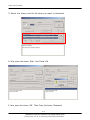
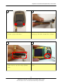
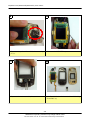
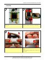
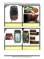
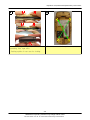
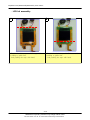
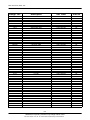
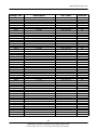
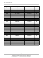
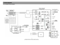
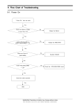
GSM TELEPHONE
SGH-E500
GSM TELEPHONE
CONTENTS
1.
Safety Precautions
2.
Specification
3.
Product Function
4.
Array course control
5.
Exploded View/Disassembly
and Assembly Instructions
6.
MAIN Electrical Parts List
7.
Block Diagrams
8.
PCB Diagrams
9.
Flow Chart of Troubleshooting
10.
Reference data
CONTENTS
1. Safety Precautions
1-1. Repair Precaution...........................................................................1-1
1-2. ESD(Electrostatically Sensitive Devices) Precaution ..........................1-2
2. Specification
2-1. GSM General Specification .............................................................2-1
2-2. GSM Tx Power Class .....................................................................2-2
3. Product Function
4. Array course control
4-1. Downloading Binary,Tfs Files .........................................................4-2
4-2. Pre-requsite for Downloading .........................................................4-2
4-3. S/W Downloader Program .............................................................4-3
5. Exploded View/Disassembly & Assembly Instructions
5-1. Cellular phone Exploded View.........................................................5-1
5-2. Cellular phone Parts list.................................................................5-2
5-3. Disassembly & Assembly Instructions..............................................5-4
6. MAIN Electrical Parts List
7. Block Diagrams
7-1. RF Solution Block Diagram.............................................................7-1
7-2. Base Band Solution Block Diagram..................................................7-2
8. PCB Diagrams
CONTENTS
9. Flow Chart of Troubleshooting
9-1. Power On......................................................................................9-1
9-2. Initial ..........................................................................................9-4
9-3. Charging Part................................................................................9-6
9-4. Sim Part.......................................................................................9-8
9-5. Microphone Part ..........................................................................9-10
9-6. Speaker Part...............................................................................9-12
9-7. Key Data Input............................................................................9-15
9-8. Receiver Part...............................................................................9-17
9-9. Back Light(for LCD)......................................................................9-19
9-10. Key Back Light...........................................................................9-21
9-11. Camera Part..............................................................................9-22
9-12. BLUETOOTh...............................................................................9-24
9-13. GSM Receiver............................................................................9-26
9-14. GSM Transmitter........................................................................9-29
9-15. DCS Receiver.............................................................................9-31
9-16. DCS Transmitter........................................................................9-33
9-17. PCS Receiver.............................................................................9-35
9-18. PCS Transmitterr........................................................................9-37
10. Reference data
1. Safety Precautions
1-1. Repair Precaution
● Repair in Shield Box, during detailed tuning.
Take specially care of tuning or test,
because specificity of cellular phone is sensitive for surrounding interference(RF noise).
● Be careful of using any kind of magnetic object or tool,
because performance of parts is damaged by the influence of magnetic force.
● Surely use a standard screwdriver when you disassemble this product,
otherwise, screw will be worn away.
● Use a thick twisted wire when you measure level.
A thick twisted wire has low resistance, therefore, a chance of measurement error is low.
● Repair after separate Test Pack & Set because of short-danger (for example an
overcurrent and furious flames of parts, etc) when you repair board in condition of
connecting Test Pack and tuning on.
● Take special care of soldering, because Land of PCB is small and weak in heat.
● Surely turn on/off the phone while using AC power plug, because a repair of battery
charger is dangerous when you turn ON/OFF PBA and Connector after disassembling charger.
● Don't use as you pleases after change other material than replacement registered on SEC System.
Otherwise engineer in charge isn't charged with problem that you don't keep this rules.
1-1
SAMSUNG Proprietary-Contents may change without notice
This Document can not be used without Samsung's authorization
Safety Precautions
1-2. ESD(Electrostatically Sensitive Devices) Precaution
Several semiconductor may be damaged easily by static electricity. Such parts are called by ESD
(Electrostatically Sensitive Devices), for example IC,BGA chip etc. Read Precaution below.
You can prevent from ESD damage by static electricity as following:
● Remove remaining static electricity on your body before you touch semiconductor or parts with
semiconductor. Please touch an earthed place or wear static electricity
prevention string on wrist.
● Use earthed soldering steel when you connect or disconnect ESD.
● Use soldering-removing tool to break static electricity ,otherwise ESD will be damaged by
static electricity.
● Don't unpack until you set up ESD on product. Because most of ESDs are packed in box and
aluminum plate to have conductive power to avoid static electricity.
● You must maintain electric contact between ESD and plate until ESD is connected
completely to the proper place or a circuit board.
1-2
SAMSUNG Proprietary-Contents may change without notice
This Document can not be used without Samsung's authorization
2. Specification
2-1. GSM General Specification
GSM 900
Phas e 1
GSM 900
Phas e 2
DCS 1800
Phas e 1
DCS 1800
Phas e 2
PCS 1900
Fr eq.
Band[ MHz]
Uplink/Downlin k
890~9 15
935~9 60
880~9 15
925~9 60
1710~ 1785
1805~ 1880
1710~ 1785
1805~ 1880
1850~ 1910
1930~ 1990
ARFCN r ange
1~12 4
0~124 &
975~1 023
512~ 885
512~ 885
512~ 810
Tx/Rx spa cing
45MHz
45MHz
95MHz
95MHz
80MHz
Mod. Da ta rate/
Bit Period
270.8 33kbps
3.69 2us
270.8 33kbps
3.69 2us
270.8 33kbps
3.6 92us
270.8 33kbps
3.6 92us
270.8 33kbps
3.6 92us
T im e Sl ot
Period/F rame
Pe rio d
576. 9us
4 .615ms
576. 9us
4 .615ms
576. 9us
4.615 ms
576. 9us
4.615 ms
576. 9us
4.615 ms
Modulatio n
0.3G MSK
0.3G MSK
0.3 GMSK
0.3 GMSK
0.3 GMSK
MS Powe r
33dBm~ 5dBm 33dBm~ 5dBm 30dBm~ 0dBm 30dBm~ 0dBm 30dBm~ 0dBm
Power Co ntr ol
level
5pcl ~ 1 9pcl
5pcl ~ 19pcl
0pcl ~ 15pcl
Sensit ivit y
- 102dBm
- 102dBm
- 100dBm
- 100dBm
- 100dBm
TDMA Mux
8
8
8
8
8
Cell Radius
35Km
35 km
2km
2km
2km
2-1
0pcl ~ 1 5pcl 0pcl ~ 1 5pcl
Speclflcation
2-2. GSM Tx Power Class
TX Power
control level
GSM900
TX Power
DCS1800
control level
TX Power
control level
PCS1800
5
33±3 dBm
0
30±3 dBm
0
30±3 dBm
6
31±3 dBm
1
28±3 dBm
1
28±3 dBm
7
29±3 dBm
2
26±3 dBm
2
26±3 dBm
8
27±3 dBm
3
24±3 dBm
3
24±3 dBm
9
25±3 dBm
4
22±3 dBm
4
22±3 dBm
10
23±3 dBm
5
20±3 dBm
5
20±3 dBm
11
21±3 dBm
6
18±3 dBm
6
18±3 dBm
12
19±3 dBm
7
16±3 dBm
7
16±3 dBm
13
17±3 dBm
8
14±3 dBm
8
14±3 dBm
14
15±3 dBm
9
12±4 dBm
9
12±4 dBm
15
13±3 dBm
10
10±4 dBm
10
10±4 dBm
16
11±5 dBm
11
8±4dBm
11
8±4 dBm
17
9±5 dBm
12
6±4 dBm
12
6±4 dBm
18
7±5 dBm
13
4±4 dBm
13
4±4 dBm
19
5±5 dBm
14
2±5 dBm
14
2±5 dBm
15
0±5 dBm
15
0±5 dBm
2-2
3. Product Function
Main Function
-Camera and camcorder
-Image editor
-MP3 player
-Phonebook
-Name card
-Multimedia Message Service (MMS)
-E-mail
-Voice recorder
-Bluetooth
-Get personal with photo caller ID
-Web browser
-Java
-Calendar
-Women's Life Software
-Voice recognition
-Voice Clarity
-Digital Data Printing
3-1
SAMSUNG Proprietary-Contents may change without notice
This Document can not be used without Samsung's authorization
Product Function
3-2
SAMSUNG Proprietary-Contents may change without notice
This Document can not be used without Samsung's authorization
4. Array course control
Test Jig (GH80-03306A)
Test Cable (GH39-00499A)
RF Test Cable (GH39-00397A)
4-1
SAMSUNG Proprietary-Contents may change without notice
This Document can not be used without Samsung's authorization
Array course control
Software Downloading
4-1. Downloading Binary, Tfs Files
• Three binary files for downloading E500.
– E500XAFH7.bin : Modem binary for communication function
& binary for user interface and various application
– E500XAFH7.tfs: Files need for each application
4-2. Pre-requsite for Downloading
• Downloader Program(OneNAND Downloader_V19_Lite.exe)
• E500 Mobile Phone
• Data Cable
• Binary, tfs files
4-2
SAMSUNG Proprietary-Contents may change without notice
This Document can not be used without Samsung's authorization
Array course control
4-3. S/W Downloader Program
1. Load the binary download program by executing the “OneNAND
Downloader_V19_Lite.exe”
2. Select the check box what you want to download and port No, download
rate.
4-3
SAMSUNG Proprietary-Contents may change without notice
This Document can not be used without Samsung's authorization
Array course control
3. Select the binary and tfs file what you want to download
4. Now press the button ‘Start’. And Power ON.
5. Now press the button ‘OK’. Then Press the button 'Download'.
4-4
SAMSUNG Proprietary-Contents may change without notice
This Document can not be used without Samsung's authorization
5. Exploded View/Disassembly&Assembly Instructions
5-1. Cellular phone Exploded View
QFR01
QWD01
QIF01
QFU01
QKP01
QCA02
QCA01
QME01
QVK01
QLC01
QMP01
QSP01
QAN05
QMO01
QAN02
QHI01
QCK01
QFL01
QMI03
QRE01
QVO01
QCR05
QSC11
QCR12
QRF01
QSC13
QCR17
QMW02
QBA01
QBA00
5-1
SAMSUNG Proprietary-Contents may change without notice
This Document can not be used without Samsung's authorization
Exploded View/Disassembly&Assembly Instructions
5-2. Cellular phone Parts List
Design LOC
Description
Sec Code
INTENNA-SGH E500
GH42-00822A
QAN05
ASSY RUBBER-INTENNA
GH98-01592A
QBA00
PMO-COVER BATTERY
GH72-30992A
QBA01
INNER BATTERY PACK-800MAH,BLK,
GH43-01850A
QCA01
UNIT-CAMERA
GH59-03121A
QCA02
UNIT-CAMERA KEY
GH59-03144A
QCK01
ASSY KEY-CAMERA
GH98-01017A
QCR05
SCREW-MACHINE
6001-001478
QCR12
SCREW-MACHINE
6001-001530
QCR17
SCREW-MACHINE
6001-001460
QFR01
ASSY ACCE-FRONT COVER
GH98-01008A
QFU01
ASSY ACCE-FOLDER UPPER
GH98-01006A
QIF01
PMO-COVER IF CONN
GH72-30993A
QKP01
ASSY ACCE-KEYPAD(SER/BRN)
GH98-01660A
QLC01
MEA-LCD MODULE KIT
GH97-06377A
QME01
UNIT-DOME SHEET
GH59-03218A
QMO01
MOTOR DC-SGHZ130
GH31-00154C
QMP01
PBA MAIN-SGH E500CMAIN
GH92-02945A
QMW02
PCT-MAIN WINDOW
GH72-30962A
QRF01
MPR-SHEET RF
GH74-23482A
QSC11
RMO-RUBBER SCREW CAP
GH73-07079A
QSC13
MPR-SHEET SCREW REAR
GH74-26301A
QSP01
SPEAKER
3001-001995
QVK01
UNIT-VOLUME KEY
GH59-03143A
QVO01
PMO-VOLUME KEY
GH72-30990A
QWD01
PCT-SUB WINDOW
GH72-30963A
QRE01
ASSY ACCE-REAR COVER
GH98-01009A
QMI03
ASSY RUBBER-MIC
GH98-01015A
QFL01
ASSY ACCE-FOLDER LOWER
GH98-01007A
QHI01
ASSY MEC-TYPE HINGE CAN
GH75-07973A
QAN02
5-2
SAMSUNG Proprietary-Contents may change without notice
This Document can not be used without Samsung's authorization
Exploded View/Disassembly&Assembly Instructions
Description
Sec Code
BAG PE
6902-000634
ADAPTOR-SGHE500,BLK,EU
GH44-01418A
S/W CD-SGHE500 PC LINK CD
GH46-00271A
UNIT-EARPHONE, SGH E500 , BRN
GH59-03356A
LABEL(P)-WATER SOAK
GH68-02026A
LABEL(P)-WATER SOAK
GH68-02026A
MANUAL-SFC
GH68-04336A
LABEL(P)-BARCODE RUSSIA
GH68-08494A
LABEL(R)-MAIN(SER)
GH68-09881B
MANUAL USERS-EU RUSSIAN
GH68-11410A
BOX-UNIT(SER)
GH69-04264B
MPR-BOHO VINYL LCD CONN
GH74-15350A
MPR-TAPE SUB WINDOW
GH74-23358A
MPR-TAPE MAIN WINDOW
GH74-23361A
MPR-TAPE LCD CONDUCTIVE L
GH74-23466A
MPR-TAPE LCD CONDUCTIVE R
GH74-23467A
MPR-TAPE LCD GOLD GASKETL
GH74-23468A
MPR-TAPE LCD GOLD GASKET R
GH74-23469A
MPR-TAPE INSULATE LCD1
GH74-23470A
MPR-TAPE INSULATE LCD2
GH74-23471A
MPR-TAPE GASKET DOME SHEET UP
GH74-23475A
MPR-TAPE GASKET DOME SHEET DOW
GH74-23476A
MPR-VINYL BOHO LOWER2
GH74-23484A
MPR-VINYL BOHO UPPER2
GH74-26138A
MPR-SPONGE LCD TAIL
GH74-26302A
MPR-SPONGE INTENNA
GH74-27279A
MPR-INSU TAPE
GH74-27307A
MPR-INSU TAPE
GH74-27308A
MPR-INSU TAPE
GH74-27465A
ASSY ACCE-SGHE500(LEATHER CASE
GH98-01955A
ASSY ACCE-HAND STRAP
GH98-01966A
5-3
SAMSUNG Proprietary-Contents may change without notice
This Document can not be used without Samsung's authorization
Exploded View/Disassembly&Assembly Instructions
5-3. Disassembly and Assembly Instructions
― Disassembly
1
2
1. Loosen a screw this six point form Rear.
1. Make the space between rear cover and
2. And remove the IF cover.
front cover using assembly stick.
2. And then widen space with hand and
separate 2 parts.
3
4
1. At first remove the connector from PBA.
1. Remove the keypad from front ass'y.
2. And disjoint PBA form front ass'y.
2. And separate the folder ass'y from front by
3. Remove the front sheet tape at front ass'y.
pushing the hinge.
5-4
SAMSUNG Proprietary-Contents may change without notice
This Document can not be used without Samsung's authorization
Exploded View/Disassembly&Assembly Instructions
5
6
1. Remove a screw cap with a pinset.
1. Insert a assembly stick to folder space after
2. Loosen a screw with driver.
pushing top side with a thumb like a picture.
8
7
1. Make the space between folder upper and
folder lower at top side using assembly
1. Separate a motor from folder lower using a
pinset.
stick.
5-5
SAMSUNG Proprietary-Contents may change without notice
This Document can not be used without Samsung's authorization
Exploded View/Disassembly&Assembly Instructions
9
10
1. Saparate a speaker from folder lower using
1. Remove the LCD EMI tape.
a pinset.
11
12
1. Separate the camera with pinset.
1. Verify all kinds of elements after finishing
disassembling
5-6
SAMSUNG Proprietary-Contents may change without notice
This Document can not be used without Samsung's authorization
Exploded View/Disassembly&Assembly Instructions
― Assembly
1
2
1. Attach 2 kind LCD insulation tape regarding
guide lines.
1. Insert LCD FPCB on folder lower.
2. Put the camera connector on sub-board.
3
1. Locking the hook from out side. (Left, Right) 1. Pushing the upside of folder ass'y for
locking
2. And twisting the bottom side of folder ass'y
for locking
5-7
SAMSUNG Proprietary-Contents may change without notice
This Document can not be used without Samsung's authorization
Exploded View/Disassembly&Assembly Instructions
5
6
1. Fasten a screw with driver.
1. Insert the 'con to con' to front cover hole.
2. Attach a 'screw cap' with a pinset and hit
2. Insert the folder ass'y to front cover using
with a Q-tip.
folder hinge.
7
8
1. Attach the 'front sheet'.
1. Connecting LCD FPCB to main PBA.
2. Put the keypad on front ass'y.
2. Put the side key and camera key after
setting the key FPCB.
5-8
SAMSUNG Proprietary-Contents may change without notice
This Document can not be used without Samsung's authorization
Exploded View/Disassembly&Assembly Instructions
9
10
1. At first locking the edge hook for rear
1. Fasten screws this four point of rear cover.
assembling. (left, right side)
2. Pushing upside of rear case for locking.
5-9
SAMSUNG Proprietary-Contents may change without notice
This Document can not be used without Samsung's authorization
Exploded View/Disassembly&Assembly Instructions
― LCD kit assembly
1
2
1. Put the insulation tape to LCD upper side
1. Put the insulation tape of LCD lower side
according to guide line.
according to guide line.
2. And pushing the tape with hand.
2. And pushing the tape with hand.
5-10
SAMSUNG Proprietary-Contents may change without notice
This Document can not be used without Samsung's authorization
6. MAIN Electrical Parts List
Design LOC
Description
SEC Code
STATUS
ANT3
BAT401
BTC501
C101
C102
C103
C104
C105
C109
C110
C112
C113
C114
C115
C116
C117
C118
C119
C120
C121
C122
C123
C124
C125
C128
C129
C130
C131
C133
C134
C135
C136
C137
C138
C200
C201
C202
C203
C204
C205
C206
C207
C208
C209
C210
C211
C212
C213
C214
C215
C304
C305
C306
ANTENNA-CHIP
BATTERY-LI(2ND)
HEADER-BATTERY
C-CER,CHIP
C-CER,CHIP
C-CER,CHIP
C-CER,CHIP
C-CER,CHIP
C-CER,CHIP
C-CER,CHIP
C-CER,CHIP
C-CER,CHIP
C-CER,CHIP
C-CER,CHIP
INDUCTOR-SMD
C-CER,CHIP
C-CER,CHIP
C-CER,CHIP
C-TA,CHIP
C-CER,CHIP
C-CER,CHIP
C-CER,CHIP
C-CER,CHIP
C-CER,CHIP
C-CER,CHIP
C-CER,CHIP
C-CER,CHIP
C-CER,CHIP
C-CER,CHIP
C-CER,CHIP
C-CER,CHIP
C-CER,CHIP
C-CER,CHIP
C-CER,CHIP
C-CER,CHIP
C-CER,CHIP
C-CER,CHIP
C-CER,CHIP
C-CER,CHIP
C-CER,CHIP
C-CER,CHIP
C-CER,CHIP
C-CER,CHIP
C-CER,CHIP
C-CER,CHIP
C-CER,CHIP
C-CER,CHIP
C-CER,CHIP
C-CER,CHIP
C-CER,CHIP
C-CER,CHIP
C-CER,CHIP
C-CER,CHIP
4202-001159
4302-001180
3711-006090
2203-000812
2203-002668
2203-000425
2203-002668
2203-000425
2203-000438
2203-000233
2203-000386
2203-000233
2203-000386
2203-001385
2703-001409
2203-005482
2203-006562
2203-000628
2404-001413
2203-000438
2203-005736
2203-005683
2203-005736
2203-000233
2203-000530
2203-000233
2203-000870
2203-000278
2203-000278
2203-005288
2203-000278
2203-000466
2203-005382
2203-002668
2203-006194
2203-006423
2203-006423
2203-005682
2203-006423
2203-006423
2203-006423
2203-006423
2203-006423
2203-006208
2203-006423
2203-006423
2203-006423
2203-005682
2203-006423
2203-006423
2203-006423
2203-006423
2203-006194
SA
SA
SA
SA
SA
SA
SA
SA
SA
SA
SA
SA
SA
SA
SA
SA
SA
SA
SA
SA
SA
SA
SA
SA
SNA
SA
SA
SA
SA
SA
SA
SA
SA
SA
SA
SA
SA
SA
SA
SA
SA
SA
SA
SA
SA
SA
SA
SA
SA
SA
SA
SA
SA
6-1
SAMSUNG Proprietary-Contents may change without notice
This Document can not be used without Samsung's authorization
Main Electrical Parts List
Design LOC
Description
SEC Code
STATUS
C316
C317
C318
C328
C350
C351
C401
C402
C403
C404
C406
C407
C408
C409
C410
C412
C413
C414
C415
C416
C417
C418
C419
C421
C422
C423
C424
C425
C501
C502
C503
C504
C505
C506
C507
C508
C509
C602
C603
C605
C606
C607
C608
C610
C611
C612
C613
C614
C615
C616
C617
C618
C619
C-CER,CHIP
C-CER,CHIP
C-CER,CHIP
C-TA,CHIP
C-CER,CHIP
C-CER,CHIP
C-CER,CHIP
C-CER,CHIP
C-CER,CHIP
C-CER,CHIP
C-CER,CHIP
C-CER,CHIP
C-CER,CHIP
C-CER,CHIP
C-CER,CHIP
C-CER,CHIP
C-CER,CHIP
C-CER,CHIP
C-CER,CHIP
C-CER,CHIP
C-CER,CHIP
C-CER,CHIP
C-CER,CHIP
C-CER,CHIP
C-CER,CHIP
C-CER,CHIP
C-CER,CHIP
C-CER,CHIP
C-CER,CHIP
C-CER,CHIP
C-CER,CHIP
C-CER,CHIP
C-CER,CHIP
C-CER,CHIP
C-CER,CHIP
C-CER,CHIP
C-CER,CHIP
C-CER,CHIP
C-CER,CHIP
C-CER,CHIP
C-CER,CHIP
C-CER,CHIP
C-CER,CHIP
C-CER,CHIP
C-CER,CHIP
C-CER,CHIP
C-CER,CHIP
C-CER,CHIP
C-CER,CHIP
C-CER,CHIP
C-CER,CHIP
C-CER,CHIP
C-CER,CHIP
2203-006423
2203-000438
2203-006423
2404-001240
2203-006324
2203-006324
2203-006825
2203-005819
2203-005819
2203-006825
2203-005482
2203-006257
2203-000425
2203-000233
2203-000425
2203-000812
2203-006838
2203-006257
2203-006838
2203-006257
2203-006257
2203-006208
2203-005482
2203-006838
2203-006208
2203-006838
2203-006257
2203-006257
2203-000189
2203-000854
2203-000854
2203-005482
2203-005382
2203-002709
2203-000995
2203-005482
2203-002443
2203-005052
2203-005054
2203-000278
2203-005819
2203-006562
2203-005050
2203-000995
2203-005052
2203-005054
2203-006562
2203-006562
2203-005052
2203-005054
2203-000278
2203-005819
2203-006562
SA
SA
SA
SA
SA
SA
SA
SA
SA
SA
SA
SA
SA
SA
SA
SA
SA
SA
SA
SA
SA
SA
SA
SA
SA
SA
SA
SA
SA
SA
SA
SA
SA
SA
SA
SA
SA
SA
SA
SA
SA
SA
SA
SA
SA
SA
SA
SA
SA
SA
SA
SA
SA
6-2
SAMSUNG Proprietary-Contents may change without notice
This Document can not be used without Samsung's authorization
Main Electrical Parts List
Design LOC
Description
SEC Code
STATUS
C620
C621
C622
C623
C624
C625
C626
C627
C628
C629
C632
C635
C637
C638
C641
C702
C703
C705
C706
C707
C708
C709
C710
C712
C713
C714
C715
C716
C717
C718
C719
C720
C721
D601
F100
F600
F700
F701
F702
F703
F704
F705
IFC600
L100
L101
L103
L104
L106
L107
L108
L109
L110
L111
C-CER,CHIP
C-CER,CHIP
C-CER,CHIP
C-CER,CHIP
C-CER,CHIP
C-CER,CHIP
C-CER,CHIP
C-CER,CHIP
C-CER,CHIP
C-CER,CHIP
C-CER,CHIP
C-CER,CHIP
C-CER,CHIP
C-TA,CHIP
C-CER,CHIP
C-CER,CHIP
C-CER,CHIP
C-CER,CHIP
C-CER,CHIP
C-CER,CHIP
C-CER,CHIP
C-CER,CHIP
C-CER,CHIP
C-CER,CHIP
C-CER,CHIP
C-CER,CHIP
C-CER,CHIP
C-CER,CHIP
C-CER,CHIP
C-CER,CHIP
C-CER,CHIP
C-CER,CHIP
C-CER,CHIP
DIODE-SCHOTTKY
FILTER-SAW
FILTER-EMI/ESD
FILTER-EMI SMD
FILTER-EMI SMD
FILTER-EMI SMD
FILTER-EMI SMD
FILTER-EMI SMD
FILTER-EMI SMD
SOCKET-INTERFACE
NPR-ANTENNA CONTACT V2
NPR-ANTENNA CONTACT V2
INDUCTOR-SMD
INDUCTOR-SMD
INDUCTOR-SMD
INDUCTOR-SMD
INDUCTOR-SMD
INDUCTOR-SMD
INDUCTOR-SMD
INDUCTOR-SMD
2203-005052
2203-005054
2203-000995
2203-000278
2203-006137
2203-000438
2203-000438
2203-005682
2203-005682
2203-005682
2203-002709
2203-002709
2203-000254
2404-001383
2203-000254
2203-006838
2203-006562
2203-006423
2203-006423
2203-006423
2203-006423
2203-005717
2203-005717
2203-005717
2203-005717
2203-005717
2203-005717
2203-005717
2203-005683
2203-005683
2203-005683
2203-005683
2203-005683
0404-001172
2904-001553
2901-001349
2901-001377
2901-001377
2901-001377
2901-001377
2901-001377
2901-001377
3710-002306
GH71-06570A
GH71-06570A
2703-001938
2703-002200
2703-001613
2703-001750
2703-001750
2703-001748
2703-002636
2703-002281
SA
SA
SA
SA
SA
SA
SA
SA
SA
SA
SA
SA
SA
SA
SA
SA
SA
SA
SA
SA
SA
SNA
SNA
SNA
SNA
SNA
SNA
SNA
SA
SA
SA
SA
SA
SA
SA
SA
SA
SA
SA
SA
SA
SA
SA
SA
SA
SA
SA
SA
SA
SA
SA
SA
SA
6-3
SAMSUNG Proprietary-Contents may change without notice
This Document can not be used without Samsung's authorization
Main Electrical Parts List
Design LOC
Description
SEC Code
STATUS
L113
L115
L116
L117
L300
L400
L402
L404
L500
L600
L601
LED611
LED613
MIC600
MOD1
MODULE100
OSC400
PAM100
R100
R101
R102
R104
R105
R106
R107
R108
R109
R110
R111
R112
R113
R117
R118
R119
R120
R121
R122
R123
R200
R202
R204
R205
R206
R207
R208
R210
R294
R300
R301
R302
R303
R304
R307
INDUCTOR-SMD
INDUCTOR-SMD
BEAD-SMD
INDUCTOR-SMD
BEAD-SMD
BEAD-SMD
INDUCTOR-SMD
R-CHIP
BEAD-SMD
BEAD-SMD
BEAD-SMD
LED
LED
MIC-CONDENSOR
BLUETOOTH MODULE
DUPLEXER-FEM
CRYSTAL-SMD
IC-POWER AMP
R-CHIP
R-CHIP
R-CHIP
R-CHIP
R-CHIP
R-CHIP
R-CHIP
R-CHIP
R-CHIP
R-CHIP
R-CHIP
R-CHIP
R-CHIP
R-CHIP
R-CHIP
R-CHIP
R-CHIP
R-CHIP
R-CHIP
R-CHIP
R-CHIP
R-CHIP
R-CHIP
R-CHIP
R-CHIP
R-CHIP
R-CHIP
R-CHIP
R-CHIP
R-CHIP
R-CHIP
R-CHIP
R-CHIP
R-CHIP
R-CHIP
2703-002198
2703-002313
3301-001729
2703-002267
3301-001534
3301-001120
2703-002782
2007-000171
3301-001534
3301-001158
3301-001158
0601-002119
0601-002119
3003-001107
4709-001445
2911-000046
2801-004466
1201-002280
2007-000171
2007-008542
2007-008542
2007-008542
2007-000148
2007-000172
2007-000566
2007-000566
2007-007190
2007-007318
2007-007155
2007-007155
2007-000171
2007-008542
2007-008542
2007-008542
2007-008542
2007-007190
2007-007155
2007-007155
2007-008516
2007-008055
2007-008478
2007-008478
2007-008055
2007-008055
2007-008052
2007-008516
2007-008055
2007-008055
2007-000168
2007-008516
2007-008052
2007-008052
2007-008055
SA
SA
SA
SA
SA
SA
SA
SA
SA
SA
SA
SA
SA
SA
SA
SA
SA
SA
SA
SA
SA
SA
SA
SA
SA
SA
SA
SA
SNA
SNA
SA
SA
SA
SA
SA
SA
SNA
SNA
SA
SA
SA
SA
SA
SA
SA
SA
SA
SA
SA
SA
SA
SA
SA
6-4
SAMSUNG Proprietary-Contents may change without notice
This Document can not be used without Samsung's authorization
Main Electrical Parts List
Design LOC
Description
SEC Code
STATUS
R309
R310
R311
R336
R337
R400
R402
R403
R505
R507
R508
R509
R511
R512
R513
R514
R515
R516
R517
R518
R519
R600
R601
R602
R603
R604
R606
R626
R627
R630
R631
R633
R634
R635
R636
R637
R640
R641
R642
R643
R644
R645
R646
R647
R648
R649
R650
R651
RFS101
SIM400
SLC600
TA411
TA423
R-CHIP
R-CHIP
R-CHIP
R-CHIP
R-CHIP
R-CHIP
R-CHIP
R-CHIP
R-CHIP
R-CHIP
R-CHIP
R-CHIP
R-CHIP
R-CHIP
R-CHIP
R-CHIP
R-CHIP
R-CHIP
R-CHIP
R-CHIP
R-CHIP
R-CHIP
R-CHIP
R-CHIP
R-CHIP
R-CHIP
R-CHIP
R-CHIP
R-CHIP
R-CHIP
R-CHIP
R-CHIP
R-CHIP
R-CHIP
R-CHIP
R-CHIP
R-CHIP
R-CHIP
R-CHIP
R-CHIP
R-CHIP
R-CHIP
R-CHIP
R-CHIP
R-CHIP
R-CHIP
R-CHIP
R-CHIP
CONNECTOR-COAXIAL
CONNECTOR-CARD EDGE
HEADER-BOARD TO BOARD
C-TA,CHIP
C-TA,CHIP
2007-007014
2007-001303
2007-007014
2007-000166
2007-000165
2007-007100
2007-000162
2007-002796
2007-000162
2007-007107
2007-000148
2007-000152
2007-000170
2007-000170
2007-000137
2007-007573
2007-000162
2007-007334
2007-008275
2007-007489
2007-007107
2007-000162
2007-000141
2007-007190
2007-000148
2007-000141
2007-007190
2007-000162
2007-001339
2007-000171
2007-000171
2007-000148
2007-000151
2007-000151
2007-000148
2007-002796
2007-002796
2007-000170
2007-000758
2007-000162
2007-000141
2007-000171
2007-000148
2007-000171
2007-000141
2007-000148
2007-000165
2007-000140
3705-001358
3709-001451
3711-005873
2404-001381
2404-001377
SA
SA
SA
SA
SA
SA
SA
SA
SA
SA
SA
SA
SA
SA
SA
SA
SA
SA
SA
SA
SA
SA
SA
SA
SA
SA
SA
SA
SA
SA
SA
SA
SA
SA
SA
SA
SA
SA
SA
SA
SA
SA
SA
SA
SA
SA
SA
SA
SA
SA
SA
SA
SA
6-5
SAMSUNG Proprietary-Contents may change without notice
This Document can not be used without Samsung's authorization
Main Electrical Parts List
Design LOC
Description
SEC Code
STATUS
TA505
TA600
TA601
TA602
TA603
TCX100
TR300
U302
U304
U308
U400
U402
U403
U501
U502
U503
U504
U602
U603
U613
U614
U701
U702
UCP200
UME300
UPL102
VR300
VR302
VR303
VR400
VR500
ZD500
ZD600
ZD601
ZD602
ZD603
ZD604
ZD605
ZD701
ZD702
ZD703
ZD705
ZD706
ZD707
ZD714
C-TA,CHIP
C-TA,CHIP
C-TA,CHIP
C-TA,CHIP
C-TA,CHIP
OSCILLATOR-VCTCXO
FET-SILICON
IC-CMOS LOGIC
IC ASIC-SPHA800
IC-CMOS LOGIC
IC-POWER SUPERVISOR
IC-POSI.FIXED REG.
IC-DC/DC CONVERTER
IC-HALL EFFECT S/W
TR-DIGITAL
FILTER-EMI SMD
IC-BATTERY
IC-POSI.FIXED REG.
IC-AUDIO AMP
IC-ANALOG MULTIPLEX
IC-ANALOG SWITCH
IC-POSI.FIXED REG.
R-CHIP
IC-COMM. CONTROLLER
IC-MCP
IC-TRANSCEIVER
DIODE-TVS
DIODE-TVS
DIODE-TVS
VARISTOR
THERMISTOR-NTC
DIODE-ZENER
DIODE-TVS
DIODE-TVS
DIODE-TVS
DIODE-TVS
DIODE-TVS
DIODE-TVS
DIODE-TVS
DIODE-TVS
DIODE-TVS
DIODE-TVS
DIODE-TVS
DIODE-TVS
DIODE-TVS
2404-001385
2404-001377
2404-001381
2404-001381
2404-001377
2809-001287
0505-001518
0801-002237
GH13-00030A
0801-002237
1203-003882
1203-003737
1203-003545
1009-001018
0504-001151
2901-001315
1203-003742
1203-003105
1201-002233
1001-001405
1001-001362
1203-003208
2007-000162
1205-002757
1108-000030
1205-002817
0406-001231
0406-001231
0406-001231
1405-001082
1404-001221
0403-001547
0406-001231
0406-001237
0406-001231
0406-001231
0406-001231
0406-001231
0406-001231
0406-001231
0406-001231
0406-001231
0406-001231
0406-001231
0406-001231
SA
SA
SA
SA
SA
SA
SA
SA
SA
SA
SA
SA
SA
SA
SA
SA
SA
SA
SA
SA
SA
SA
SA
SA
SA
SA
SA
SA
SA
SA
SA
SA
SA
SNA
SA
SA
SA
SA
SA
SA
SA
SA
SA
SA
SA
6-6
SAMSUNG Proprietary-Contents may change without notice
This Document can not be used without Samsung's authorization
7. Block Diagrams
7-1. RF Solution Block Diagram
7-1
SAMSUNG Proprietary-Contents may change without notice
This Document can not be used without Samsung's authorization
Block Diagrams
7-2. Base Band Solution Block Diagram
7-2
SAMSUNG Proprietary-Contents may change without notice
This Document can not be used without Samsung's authorization
8. PCB Diagrams
8-1. Top
8-1
PCB Diagrams
8-2. Bottom
8-2
9. Flow Chart of Troubleshooting
9-1. Power On
' Power On ' does not work
Yes
No
Check the Battery Voltage
Change the Battery
is more than 3.4V
Yes
No
Check VINT
C407 = 2.7V
Change the Battery
Yes
No
C425(+VDD_IO_LOW)=1.8V
C424(+VDD_IO_HIGH)=2.9V
Change the PMU (U400)
Yes
No
Check the Clock at
Resolder OSC400
R400=32KHZ
Yes
No
C400(+VDD_GSM_CORE)
Check the circuit related to U403
= 1.8V?
Yes
No
Check the clock (VCTCXO)
Check the circuit related to TCX100
C109 = 26MHz
Yes
Check the initial operation
Yes
END
9-1
SAMSUNG Proprietary-Contents may change without notice
This Document can not be used without Samsung's authorization
Flow Chart of Troubleshooting
9-2
SAMSUNG Proprietary-Contents may change without notice
This Document can not be used without Samsung's authorization
Flow Chart of Troubleshooting
9-3
SAMSUNG Proprietary-Contents may change without notice
This Document can not be used without Samsung's authorization
Flow Chart of Troubleshooting
9-2. Initial
Initial Failure
Yes
Check the Battery Voltage
No
Change the Battery
is more than 3.4V
Yes
No
UCP200 pin 12
(RSTON)="H",
TP229
Change the U400 (PMU)
Yes
Check U400 pin 4
No
= 32KHz
Check the circuit related to clock
Yes
No
UCP200
R204, R205, R206 is OK?
Check the UCP200
Yes
Check the 16bit data signal
Yes
END
9-4
SAMSUNG Proprietary-Contents may change without notice
This Document can not be used without Samsung's authorization
Flow Chart of Troubleshooting
9-5
SAMSUNG Proprietary-Contents may change without notice
This Document can not be used without Samsung's authorization
Flow Chart of Troubleshooting
9-3. Charging Part
Abnormal charging part
Yes
No
Check the U504 pin 1
> 4.9V
Check the circuit related to
V_EXT_CHARGE
Yes
No
U504 pin 5 (CHG_ON) = "L"?
Check UCP200
(related CHG_ON signal)
Yes
No
U504 pin 3 (AUX_ON)
Check the circuit related to
= "L"?
AUX_ON signal
Yes
Check the U504 pin 10
No
Resolder or replace U504
≒ 4.2V
Yes
END
9-6
SAMSUNG Proprietary-Contents may change without notice
This Document can not be used without Samsung's authorization
Flow Chart of Troubleshooting
BATTERY CHARGING
9-7
SAMSUNG Proprietary-Contents may change without notice
This Document can not be used without Samsung's authorization
Flow Chart of Troubleshooting
9-4. Sim Part
Phone can't access SIM Card
Yes
No
SIM400 pin 1,5 = "H"?
Change U400
Yes
After SIM card insert,
No
SIM400 pin 2 = "H(SIM_RST)"?
Change U400
Yes
After Power ON,
No
Check SIMCLK Signal on
Check the Clock
pin3 of SIM400 in a few second
Yes
Check the SIM Card
Yes
END
9-8
SAMSUNG Proprietary-Contents may change without notice
This Document can not be used without Samsung's authorization
Flow Chart of Troubleshooting
9-9
SAMSUNG Proprietary-Contents may change without notice
This Document can not be used without Samsung's authorization
Flow Chart of Troubleshooting
9-5. Microphone Part
Microphone does not work
Yes
No
Check the connection status
of MIC600,
Resolder MIC600
Yes
Check MIC_BIAS
No
Resolder
TA600, R403, R644, R640, R648, R645, R647,
= "H" ?
C607, C613
Yes
Check the MIC600
No
Replace the MIC600
Yes
END
9-10
SAMSUNG Proprietary-Contents may change without notice
This Document can not be used without Samsung's authorization
Flow Chart of Troubleshooting
9-11
SAMSUNG Proprietary-Contents may change without notice
This Document can not be used without Samsung's authorization
Flow Chart of Troubleshooting
9-6. Speaker Part (Melody)
Speaker does not work
Yes
No
Check
Pin A1, C1 of the U603
(R634, R635)
Resolder C637, C641, R634, R635
Yes
No
Check Pin A3, C3
of the U603
(L600, L601)
check the U603
Yes
No
Check the U613
Pin 7, 11
Resolder L600, L601
Yes
No
Check the U613
Pin 8, 12
check the U613
Yes
No
Check the LCD connector
Pin 50, 52
Resolder SLC600
Yes
No
Check LCD Module
Replace LCD Module
Yes
No
Replace SPK
Check speaker
Yes
END
9-12
SAMSUNG Proprietary-Contents may change without notice
This Document can not be used without Samsung's authorization
Flow Chart of Troubleshooting
9-13
SAMSUNG Proprietary-Contents may change without notice
This Document can not be used without Samsung's authorization
Flow Chart of Troubleshooting
9-14
SAMSUNG Proprietary-Contents may change without notice
This Document can not be used without Samsung's authorization
Flow Chart of Troubleshooting
9-7. Key Data Input
Check Initial Operation
Yes
When one of the keys is
No
pushed,
Check the Dome sheet & Key Pad
Isn't it displayed on LCD?
Yes
When one of the keys is
pushed,
No
Resolder ZD705, ZD706, ZD707
KEY_ROW(0,4),
KEY_COL(0,4)
signal is OK?
Yes
END
9-15
SAMSUNG Proprietary-Contents may change without notice
This Document can not be used without Samsung's authorization
Flow Chart of Troubleshooting
9-16
SAMSUNG Proprietary-Contents may change without notice
This Document can not be used without Samsung's authorization
Flow Chart of Troubleshooting
9-8. Receiver Part
Receiver does not work
Yes
No
Check the U613
Pin 1, 5 = 1.5V?
(HFR_P, N)
Resolder UCP200 or change PBA
Yes
No
Check the U613
Pin 4, 9, 13, 16 = 1.5V
Resolder or replace the U613
Yes
No
Check the U613
Pin 8, 12 = 1.5V?
Resolder or replace the U613
Yes
Check the LCD connector
(SCL600)
Pin 50, 52 = 1.5V
No
Change the LCD connector
Yes
No
LCD MODULE
SPK +,- PAD = 1.5V?
Change the LCD module
Yes
Check the soldering of the
No
Modify the speaker wire soldering
speaker wire
Yes
No
Is Receiver working ?
Replace the Speaker
Yes
END
9-17
SAMSUNG Proprietary-Contents may change without notice
This Document can not be used without Samsung's authorization
Flow Chart of Troubleshooting
9-18
SAMSUNG Proprietary-Contents may change without notice
This Document can not be used without Samsung's authorization
Flow Chart of Troubleshooting
9-9. Back Light (for Color Main LCD)
Backlight does not work
Yes
No
Is LCD Contrast set on high
level in the Menu?
Set LCD Contrast on high level
Yes
No
U1 pin 8 (LCD_BL_ON)
Change the board to board
= "H" ?
Connector
Yes
No
Check the U1 & the related circuit
U1 PIN 14 = 6.3V ?
Yes
Replace the LCD Module
Yes
END
9-19
SAMSUNG Proprietary-Contents may change without notice
This Document can not be used without Samsung's authorization
Flow Chart of Troubleshooting
9-20
SAMSUNG Proprietary-Contents may change without notice
This Document can not be used without Samsung's authorization
Flow Chart of Troubleshooting
9-10. Key Back Light
Main Key LED does not work
Yes
U602 pin 3 (key_LED_ON)
= "H"?
No
Check the UCP200 related to
"KEY_LED_ON"
No
Replace U602
Yes
U602 pin 1 = "H" ?
Yes
END
9-21
SAMSUNG Proprietary-Contents may change without notice
This Document can not be used without Samsung's authorization
Flow Chart of Troubleshooting
9-11. Camera part
Camera does not work
Yes
No
Check the Camera
Reconnect the camera module
connector status
Yes
No
SLC600 Pin 42 = 1.8V?
Check the U701
Yes
No
SLC600 Pin 40 = 2.8V?
Check the U400
Yes
No
Check the camera module
Replace the Camera Module
Yes
Yes
Is there another problem?
Change the PBA
No
END
9-22
SAMSUNG Proprietary-Contents may change without notice
This Document can not be used without Samsung's authorization
Flow Chart of Troubleshooting
9-23
SAMSUNG Proprietary-Contents may change without notice
This Document can not be used without Samsung's authorization
Flow Chart of Troubleshooting
9-12. BLUETOOTH
BLUETOOTH does not work
Yes
No
MOD1
Resolder the L300, C350 or
Check the circuit related to VDD_IO_LOW
Pin 20, 16 = 1.8V ?
Yes
No
Check the circuit related BT control signal
(UCP200)
MOD1
Pin 19 (BT_EN) = "H"
Pin 11 (BT_RST) = "H"
Yes
No
MOD1
Pin 17(BT_Shutdown) = "H"
Pin 15(BT_Host_Wake) ="L"
Check the circuit related BT control signal
(UCP200)
Yes
No
MOD1
Check the circuit related clock (U400)
Pin 18 = 32 kHz ?
Yes
No
MOD1
Pin21(RXD2), Pin22(RST2),
Pin23(TXD2),Pin24(CST2) ok?
Resolder MOD1 or replace UCP200
Yes
No
Check ANT3
Replace ANT3
OK?
Yes
END
9-24
SAMSUNG Proprietary-Contents may change without notice
This Document can not be used without Samsung's authorization
Flow Chart of Troubleshooting
9-25
SAMSUNG Proprietary-Contents may change without notice
This Document can not be used without Samsung's authorization
Flow Chart of Troubleshooting
9-13. GSM Receiver
RX ON
RF input : 62CH
Amp : -50dBm
Yes
Module100 pin8
>= -65dBm
No
Resolder RFS101, C101
Yes
Module100 pin5,pin6
>= -65dBm
No
Check Module100
pin10,pin12 = L
No
Check ANT Switch
control circuit
Yes
Yes
Resolder Module100
No
UPL102
pin29 >= -70dBm
pin30 >= -70dBm
Resolder C103, C105, L106
Yes
No
UPL102 pin7,8,9,10
>= 1V
Check UPL102
pin23,26,28 >=2.7V
No
Check & Resolder
UPL102, C109
RF26MHz, RF PSU Part
Yes
Yes
Resolder UPL102
R117,R118,R119,R120
>= 1V
Yes
Check UCP200
END
9-26
SAMSUNG Proprietary-Contents may change without notice
This Document can not be used without Samsung's authorization
Flow Chart of Troubleshooting
9-27
SAMSUNG Proprietary-Contents may change without notice
This Document can not be used without Samsung's authorization
Flow Chart of Troubleshooting
9-28
SAMSUNG Proprietary-Contents may change without notice
This Document can not be used without Samsung's authorization
Flow Chart of Troubleshooting
9-14. GSM Transmitter
TX ON (5Level)
Yes
Module100 Pin8
>= 20dBm
Yes
Resolder RFS101, C101
No
Module100 pin11
>= 18dBm
Yes
Check Module100
pin10 = H (2.68V),
pin12 = L
No
Check ANT Switch
control circuit
Yes
No
PAM100 pin18
>= 18dBm
Yes
Change or Resolder
Module100
Resolder C130, L111
No
PAM100 14pin
>= -11dBm
Yes
Check PAM100
pin2, 3, 5, 7, 8, 9,
10, 15, 16 OK?
Yes
Resolder or Change PAM100
No
Check +VBAT or PAM100
control signal
No
R117,R118,R119,R120
>= 1V
No
Check UPL102
pin23,26,28 >=2.7V
Yes
No
Check & Resolder
UPL102, C109
RF26MHz, RF PSU Part
Yes
Resolder UPL102
Check UCP200
END
9-29
SAMSUNG Proprietary-Contents may change without notice
This Document can not be used without Samsung's authorization
Flow Chart of Troubleshooting
9-30
SAMSUNG Proprietary-Contents may change without notice
This Document can not be used without Samsung's authorization
Flow Chart of Troubleshooting
9-15. DCS Receiver
RX ON
RF input : 698CH
Amp : -50dBm
Yes
Module100 pin8
>= -65dBm
No
Resolder RFS101, C101
Yes
Module100 pin1,pin2
>= -65dBm
No
Check Module100
pin10,pin12 = L
No
Check ANT Switch
control circuit
Yes
Yes
Resolder Module100
UPL102
pin35 >= -70dBm
pin36 >= -70dBm
No
Resolder C112, C114, L110
Yes
UPL102 pin7,8,9,10
>= 1V
No
Check UPL102
pin23,26,28>=2.7V
No
Check & Resolder
UPL102, C109
RF26MHz, RF PSU Part
Yes
Yes
Resolder UPL102
R117,R118,R119,R120
>= 1V
Yes
Check UCP200
END
9-31
SAMSUNG Proprietary-Contents may change without notice
This Document can not be used without Samsung's authorization
Flow Chart of Troubleshooting
9-32
SAMSUNG Proprietary-Contents may change without notice
This Document can not be used without Samsung's authorization
Flow Chart of Troubleshooting
9-16. DCS Transmitter
TX ON (0Level)
Yes
Yes
Module100 pin8
>= 20dBm
Resolder RFS101, C101
No
Module100 pin13
>= 18dBm
Yes
Check Module100
pin12 = H (2.68V),
pin10 = L
No
No
Check ANT Switch
control circuit
Change or Resolder
Module100
Yes
PAM100 pin20
>= 18dBm
Yes
Resolder C102, C104, R113
No
Yes
PAM100 pin4
>= -11dBm
Check PAM100
pin2,3,5,7,8,9,10,
15, 16 OK?
Yes
Resolder or Change PAM100
No
No
R117,R118,R119,R120
>= 1V
No
Check UPL102
pin23,26,28
>=2.7V
Check +VBAT or PAM100
control signal
No
Check & Resolder
UPL102, C109
RF26MHz, RF PSU Part
Yes
Yes
Resolder UPL102
Check UCP200
END
9-33
SAMSUNG Proprietary-Contents may change without notice
This Document can not be used without Samsung's authorization
Flow Chart of Troubleshooting
9-34
SAMSUNG Proprietary-Contents may change without notice
This Document can not be used without Samsung's authorization
Flow Chart of Troubleshooting
9-17. PCS Receiver
RX ON
RF input : 661CH
Amp : -50dBm
Yes
Module100 pin8
>= -65dBm
No
Resolder RFS101, C101
Yes
Module100 pin3,pin4
>= -65dBm
No
Check Module100
pin10,pin12 = L
No
Check ANT Switch
control circuit
Yes
Yes
Resolder Module100
UPL102
pin32 >= -70dBm
pin33 >= -70dBm
No
Resolder L107, L108, C134
Yes
UPL102 pin7,8,9,10
>= 1V
No
Check UPL102
pin23,26,28 >=2.7V
No
Check & Resolder
UPL102, C109
RF26MHz, RF PSU Part
Yes
Yes
Resolder UPL102
R117,R118,R119,R120
>= 1V
Yes
Check UCP200
END
9-35
SAMSUNG Proprietary-Contents may change without notice
This Document can not be used without Samsung's authorization
Flow Chart of Troubleshooting
9-36
SAMSUNG Proprietary-Contents may change without notice
This Document can not be used without Samsung's authorization
Flow Chart of Troubleshooting
9-18. PCS Transmitter
TX ON (0Level)
Yes
Module100 Pin8
>= 20dBm
Yes
Resolder RFS101, C101
No
Module100 pin13
>= 18dBm
Yes
Check Module100
pin12 = H (2.68V),
pin10 = L
No
Check ANT Switch
control circuit
Yes
No
PAM100 pin20
>= 18dBm
Change or Resolder
Module100
Yes
Resolder C102, C104, R113
No
Yes
PAM100 pin4
>= -11dBm
Check PAM100
pin2,3,5,7,8,9,10,
15,16 OK?
Yes
Resolder or Change PAM100
No
No
R117,R118,R119,R120
>= 1V
No
Check UPL102
pin23,26,28
>=2.7V
Check +VBAT or PAM100
control signal
No
Check & Resolder
UPL102, C109
RF26MHz, RF PSU Part
Yes
Yes
Check UCP200
END
9-37
SAMSUNG Proprietary-Contents may change without notice
This Document can not be used without Samsung's authorization
Resolder UPL102
Flow Chart of Troubleshooting
9-38
SAMSUNG Proprietary-Contents may change without notice
This Document can not be used without Samsung's authorization
10. Reference data
Reference Abbreviate
― AAC: Advanced Audio Coding.
― AVC : Advanced Video Coding.
― BER : Bit Error Rate
― BPSK: Binary Phase Shift Keying
― CA : Conditional Access
― CDM : Code Division Multiplexing
― C/I : Carrier to Interference
― DMB : Digital Multimedia Broadcasting
― EN : European Standard
― ES : Elementary Stream
― ETSI: European Telecommunications Standards Institute
― MPEG: Moving Picture Experts Group
― PN : Pseudo-random Noise
― PS : Pilot Symbol
― QPSK: Quadrature Phase Shift Keying
― RS : Reed-Solomon
― SI : Service Information
― TDM : Time Division Multiplexing
― TS : Transport Stream
10-1
SAMSUNG Proprietary-Contents may change without notice
This Document can not be used without Samsung's authorization
Reference data
10-2
SAMSUNG Proprietary-Contents may change without notice
This Document can not be used without Samsung's authorization
This Service Manual is a property of Samsung Electronics Co.,Ltd.
Any unauthorized use of Manual can be punished under applicable
International and/or domestic law.
ⓒ Samsung Electronics Co.,Ltd.
2006. 09 Rev.1.0