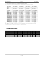
1
COM Express TM ® User Manual Compact Module MSC CXC-PV525 Intel Atom Rev.1.3 TM Type 2 Pin-out D525/D425/N455 2014-09-04 MSC CXC-PV525 Rev.1.3 User's Manual Preface Copyright Notice Copyright © 2014 MSC Technologies GmbH. All rights reserved. Copying of this document, and giving it to others and the use or communication of the contents thereof, is forbidden without express authority. Offenders are liable to the payment of damages. All rights are reserved in the event of the grant of a patent or the registration of a utility model or design. Important Information This documentation is intended for qualified audience only. The product described herein is not an end user product. It was developed and manufactured for further processing by trained personnel. Disclaimer Although this document has been generated with the utmost care no warranty or liability for correctness or suitability for any particular purpose is implied. The information in this document is provided “as is” and is subject to change without notice. EMC Rules This unit has to be installed in a shielded housing. If not installed in a properly shielded enclosure, and used in accordance with the instruction manual, this product may cause radio interference in which case the user may be required to take adequate measures at his or her owns expense. Trademarks All used product names, logos or trademarks are property of their respective owners. Certification MSC Technologies GmbH is certified according to DIN EN ISO 9001:2000 standards. Life-Cycle-Management MSC products are developed and manufactured according to high quality standards. Our lifecycle-management assures long term availability through permanent product maintenance. Technically necessary changes and improvements are introduced if applicable. A productchange-notification and end-of-life management process assures early information of our customers. Product Support MSC engineers and technicians are committed to provide support to our customers whenever needed. Before contacting Technical Support of MSC Technologies GmbH, please consult the respective pages on our web site at www.msc-technologies.eu for the latest documentation, drivers and software downloads. If the information provided there does not solve your problem, please contact our Technical Support: Email: [email protected] Phone: +49 8165 906-200 2 / 61 MSC CXC-PV525 Rev.1.3 User's Manual Content 1 General Information ..................................................................................................... 5 1.1 Revision History........................................................................................................ 5 1.2 Reference Documents .............................................................................................. 5 1.3 Introduction............................................................................................................... 6 2 Technical Description................................................................................................... 7 2.1 Key Features ............................................................................................................ 7 2.2 Block diagram........................................................................................................... 8 2.3 Com Express Implementation ................................................................................... 8 2.4 Functional Units ...................................................................................................... 10 2.5 System Memory...................................................................................................... 11 2.6 Power Supply ......................................................................................................... 11 2.7 Current Dissipation ................................................................................................. 11 2.8 Mechanical Dimensions .......................................................................................... 12 2.8.1 Compact module .............................................................................................. 12 2.9 Thermal specifications ............................................................................................ 13 2.9.1 Environment ..................................................................................................... 13 2.10 Installation ........................................................................................................... 14 2.10.1 Jumpers and switches................................................................................... 14 2.10.2 Installing a DDR3 SO-DIMM module ............................................................. 15 2.10.3 Optional SATA NAND Flash.......................................................................... 15 2.11 Watchdog ............................................................................................................ 15 2.12 Signal description ................................................................................................ 16 2.12.1 High Definition Audio .................................................................................... 16 2.12.2 Ethernet ........................................................................................................ 16 2.12.3 IDE................................................................................................................ 17 2.12.4 Serial ATA..................................................................................................... 17 2.12.5 PCI Express Lanes ....................................................................................... 18 2.12.6 PCI Express Lanes x16................................................................................. 18 2.12.7 Express Card Support ................................................................................... 18 2.12.8 PCI Bus ........................................................................................................ 19 2.12.9 USB .............................................................................................................. 20 2.12.10 LVDS Flat Panel ........................................................................................... 20 2.12.11 LPC Bus ....................................................................................................... 20 2.12.12 Analog VGA .................................................................................................. 21 2.12.13 SPI Interface ................................................................................................. 21 2.12.14 Miscellaneous ............................................................................................... 21 2.12.15 Power and System Management .................................................................. 22 2.12.16 General Purpose I/O ..................................................................................... 22 2.12.17 Module Type Definition ................................................................................. 23 2.12.18 Power and GND ............................................................................................ 23 2.13 Pin List for MSC CXC-PV525 module (Type 2).................................................... 24 3 System resources ...................................................................................................... 26 3.1 PCI IRQ Routing ..................................................................................................... 26 3.2 Carrier Board PCI Resource Allocation ................................................................... 27 3.3 SMB Address Map.................................................................................................. 27 4. Connectors ............................................................................................................. 28 4.2 Connector X5 (FAN) ............................................................................................... 28 5. BIOS....................................................................................................................... 29 5.2 Introduction............................................................................................................. 29 5.2.1 Startup Screen Overview ................................................................................. 29 5.2.2 Activity Detection Background .......................................................................... 29 5.3 TrustedCore Setup Utility........................................................................................ 30 5.3.1 Configuring the System BIOS........................................................................... 30 5.3.2 The Main Menu ................................................................................................ 32 3 / 61 MSC CXC-PV525 Rev.1.3 User's Manual 5.3.2.1 Board Information ...................................................................................... 33 5.3.2.2 Drive Settings ............................................................................................ 34 5.3.2.3 Keyboard Features .................................................................................... 35 5.3.2.4 Boot Features ............................................................................................ 36 5.3.3 The Advanced Menu ........................................................................................ 36 5.3.3.1 Cache Memory .......................................................................................... 38 5.3.3.2 CPU Control Sub-Menu ............................................................................. 38 Note: Some options can be different dependent on used type of CPU ! ..................... 38 5.3.3.3 Video (Intel IGD) Control Sub-Menu .......................................................... 39 5.3.3.4 ICH Control Sub Menu ............................................................................... 40 5.3.3.5 PNP Configuration ..................................................................................... 42 5.3.3.6 ACPI Control Sub-Menu ............................................................................ 43 5.3.3.7 Integrated Device Control Sub-Menu ......................................................... 44 5.3.3.7.1 PCI Express Sub-Menu ............................................................................. 45 5.3.3.7.2 ICH USB Control Sub-Menu ...................................................................... 46 5.3.3.8 I/O Device Configuration Menu .................................................................. 46 5.3.3.9 Clock Control Sub-Menu ............................................................................ 47 5.3.3.10 Watchdog Options ..................................................................................... 47 5.3.4 The Security Menu ........................................................................................... 49 5.3.5 The Power Menu .............................................................................................. 50 5.3.5.1 Hardware Monitor ...................................................................................... 50 5.3.6 The Boot Menu................................................................................................. 51 5.3.7 The Exit Menu .................................................................................................. 52 5.4 Bios Update ............................................................................................................ 53 5.5 Bios Crisis Recovery .............................................................................................. 53 5.6 Diagnostics Postcodes ........................................................................................... 57 5.6.1 Bootblock Bios Postcodes ................................................................................ 57 5.6.2 System Bios Postcodes.................................................................................... 57 5.6.3 Memory Detection Postcodes........................................................................... 61 5.6.4 ACPI Postcodes ............................................................................................... 61 4 / 61 MSC CXC-PV525 Rev.1.3 User's Manual 1 General Information 1.1 1.2 Revision History Rev. Date Description 1.0 1.1 1.2 1.3 2011-10-28 2012-03-13 2013-10-11 2014-09-04 Final Revision Marked the default setup values Added supported SIO, changed Contact Information New covering page Reference Documents [1] COM Express Module Base Specification COM Express Revision 1.0 Last update: July 10th, 2005 [2] PCI Local Bus Specification Rev. 2.1 PCI21.PDF Last update: June 1st, 1995 http://www.pcisig.com [3] ATA/ATAPI-6 Specification d1410r3b.pdf http://www.t13.org/ [4] Serial ATA Specification Serial ATA 1.0 gold.pdf Last update: August 29th, 2002 Rev.1.0 http://www.sata-io.org/ [5] IEEE Std. 802.3-2002 802.3-2002.pdf http://www.ieee.org [6] Universal Bus Specification usb_20.pdf Last update: April 27th, 2000 http://www.usb.org 5 / 61 MSC CXC-PV525 1.3 Rev.1.3 User's Manual Introduction COM Express™, an open specification of the PICMG (PCI Industrial Computer Manufacturer Group), is a module concept to bring PCI Express and other latest technologies like SATA, USB 2.0 and LVDS on a COM (Computer On Module). A COM Express™ module is plugged onto an application-specific base board similar to the ETX concept, but offers more options and a growth path to future CPU technologies. Utilizing different sizes, COM Express™ can be used for highly embedded solutions up to high performance platforms. The MSC CXC-PV525 is based on Intel AtomTM CPUs N455, D425 and D525 with the Intel I/O Controller Hub 8 Mobile (ICH8M). These Intel AtomTM CPUs are on the Intel embedded roadmap of, which means that the processors are available long term. The CXC-PV525 supports DDR3 memory modules. It provides two 204-pin SO-DIMM sockets providing the flexibility to configure the system up to 4GB of DDR3-DRAM. The integrated graphics controller contains a refresh of the 3rd generation graphics core. An analog RGB and a single LVDS channel are supported by this GPU. For evaluation and design-in of the COM Express™ modules we provide evaluation baseboards and develop motherboards providing the interface infrastructure for the COM Express™ module offering PC type connectors for external access. Up to 440 pins of connectivity are available between COM Express™ modules and the Carrier Board. Legacy buses such as PCI, parallel ATA, LPC, HDA are supported as well as new high speed serial interconnects such as PCI Express, Serial ATA and Gigabit Ethernet. To enhance interoperability between COM Express™ modules and Carrier Boards, five common signaling configurations (pin-out types) have been defined to ease system integration. 6 / 61 MSC CXC-PV525 Rev.1.3 User's Manual 2 Technical Description Key Features 2.1 The MSC CXC-PV525 COM Express module is designed as a type 2 module. Key features include: Module size 95 mm x 95 mm 18 mm ‘z’ height with heat-spreader (with 5 mm stack option) Dual 220 pin connector (440 pins) 2x DDR3 SO-DIMM module Eight USB 2.0 ports; four shared over-current lines Three Serial ATA ports with data rates up to 3.0Gb/s (300MB/s) Five PCI Express x1 lanes Support pins for two Express Cards One single channel 18-bit LVDS interface Analog VGA High definition digital audio interface (external codec) GBit Ethernet interface LPC interface Four GPI pins Four GPO pins +6V to +18V primary power supply input +5V standby (optional) and 3.3V RTC power supply inputs 32 bit PCI interface IDE port (to support legacy ATA devices such as CD-ROM drives and Compact Flash storage cards) TPM module (option, TPM 1.2, SLB9635) Automatic fan control On module SATA NAND flash (option) Support for following Super IO : Winbond 83627HG ( Device ID 0x52) 7 / 61 MSC CXC-PV525 Rev.1.3 2.2 Block diagram 2.3 Com Express Implementation User's Manual COM Express™ required and optional features of pin-out type 2 are summarized in the following table. The features identified as minimum (Min.) shall be implemented by all modules. Features identified up to maximum (Max) may be additionally implemented by a module. The column MSC CXC-PV525 shows the implemented features of the MSC module: Function MSC CXCPV525 Type 2 Note Min / Max System I/O PCI Express Graphics (PEG) PCI Express Lanes 0 - 5 PCI Express Lanes 16-31 (same as PEG pins) SDVO Channels LVDS Channels VGA Port TV-Out PATA Port 0/1 0 1/6 5 x1 0 / 16 0 0/2 0/2 0/1 NA 1/1 0 1 1 0 1 SATA Ports 2/4 3 Digital Audio Interface USB 2.0 Ports LAN 0 (10/100Base-T min) PCI Bus - 32 Bit Express Card Support 0/1 4/8 1/1 1/1 1/2 1 8 1 1 2 8 / 61 (Option 1 x4, 1 x1) 1x single channel, 18 bit (There are only two SATA ports available, when SSD option is used.) High Definition Audio 82567V Gigabit LAN MSC CXC-PV525 LPC Bus Rev.1.3 User's Manual 1/1 1 4/4 4/4 1/1 1/1 0/1 1/1 4 4 1 1 1 1 0/1 1 1/1 1 Power Management Thermal Protection Battery Low Alarm Suspend Wake Power Button Support Power Good 0/1 0/1 0/1 0/2 1/1 1/1 1 1 1 2 1 1 Security TPM (on request) 0/0 1 System Management General Purpose Inputs General Purpose Outputs SMBus I2C Watch Dog Timer Speaker Out External BIOS ROM support Reset Functions 9 / 61 WOL, PCI Wake TPM 1.2 module MSC CXC-PV525 2.4 Rev.1.3 User's Manual Functional Units CPUs Intel® Atom TM Processor soldered. D525, 1.8GHz, dual core, 400MHz GPU, DMI D425, 1.8GHz, single core, 400MHz GPU, DMI N455, 1.66GHz, single core, 200MHz GPU, DMI Chipset Intel Memory Two 204-pin DDR3 SO-DIMM sockets for up to 4GB (max. height 1250mil = 31.75mm) SATA 3 SATA channels up to 300MByte/s each EIDE 1 Enhanced IDE port ATA/UDMA100 USB 8 x USB 2.0 COM Express™ Type 2 interface, fully compliant PCI Express™ Five channels PCIe x1 PCI 32 Bit standard interface LPC Low Pin Count Bus for heritage interfaces Graphics Integrated Graphics Engine DirectX® 9 compliant Pixel Shader 2.0 MPEG2 Hardware Acceleration Video Memory Intel® Dynamic Video Memory Technology 4.0 LCD Interface LVDS 1x18Bit, single channel, max. resolution 1.366 x 768 CRT Interface max resolution 2.048 x 1.536 @ 60 Hz Ethernet 10/100/1000Base-TX (Intel® 82567V) Sound Interface High Definition Audio interface Watchdog Timer PIC12C509A generates reset (programmable, 1s … 255h) 1 ® 82801GBM ICH8 M SATA Flash optional SATA Flash disk, up to 16 GB, TPM (option) optional TPM module, TPM 1.2, SLB9635 Fan Supply 3-pin header (12V) Real Time Clock integrated in ICH 8 M EDID-EEPROM on board EDID EEPROM, enable / disable via SETUP BIOS Phoenix BIOS in SPI Flash device EEPROM EEPROM for CMOS setup backup RTC / CMOS integrated in Intel Battery external System Monitoring Voltage, Temperature, Fan 1 82801HEM ICH8 M, (typ. 2.7 µA) Core voltage 12V (Vin) CPU thermal diode Memory temperature sensor Board temperature sensor Automatic Fan Control reduces available SATA channels 10 / 61 MSC CXC-PV525 Rev.1.3 User's Manual System Memory 2.5 The MSC CXC-PV525 CPU module provides two sockets for memory modules which have to meet the following demands: 204pin unbuffered DDR3 SO-DIMM 1.5V supply voltage DDR3-800 / PC3-6400 or faster Maximal module height: 30mm SPD (Serial Presence Detect) EEPROM Power Supply 2.6 +12V primary power supply input +5V standby Option, is not required for module operation. If not present, customer has to make sure that the supply voltages which are generated on the carrier board are switched off during suspend states, so that no current from the carrier board’s signal lines can flow to the CPU board. 3.3V RTC power supply Option, is not required for module operation. BIOS SETUP data is stored in a non volatile backup memory device (EEPROM), therefore configuration data will not get lost during power off (except for time and date information) Voltage +12V +5V Standby +3V RTC power supply 2.7 Input range +6.0V - 18.0 V +4.75V - 5.25 V +2.0V - 3.3V Current See next table max. 2A max. 6µA Current Dissipation All measurements were made by plugging a MSC CXC-PV525 module onto a MSC CXEVA2 Baseboard with a multimeter connected to the +12V Line. The module was equipped with two 1GByte memory modules. Three tests were performed: 1. Booting Dos 6.22 from an USB stick. 2. Booting Microsoft Windows XP Professional SP3 from an SATA harddrive to the desktop. 3. Booting Microsoft Windows XP Professional SP3 from an SATA harddrive and using BurnIn Test V4.0 to achieve 100% CPU load. Module (CPU) Intel® D525 Intel® D425 Intel® N455 DOS Prompt 0.86 A (10.3 W) 0.88 A (10.6 W) 0.73 A (8.8 W) Windows XP Idle 0.74 A (8.9 W) 0.77 A (9.2 W) 0.59 A (7.1 W) 11 / 61 100% CPU load 1.01 A (12.1 W) 0.90 A (10.8 W) 0.73 A (8.8 W) MSC CXC-PV525 2.8 2.8.1 Rev.1.3 User's Manual Mechanical Dimensions Compact module There are two height options defined in the COM Express specification: 5mm and 8mm. The height option is defined by the connectors on the baseboard. 12 / 61 MSC CXC-PV525 2.9 Rev.1.3 User's Manual Thermal specifications The cooling solution of a COM Express module is based on a heatspreader concept. A heatspreader is a metal plate (typically aluminium) mounted on the top of the module. The connection between this plate and the module components is typically done by thermal interface materials like phase change foils, gap pads and copper or aluminium blocks. A very good thermal conductivity is required in order to conduct the heat from the cpu and the chipset to the heatspreader plate. The heatspreader of the MSC module is thermally attached using phase change materials and small aluminium blocks filling the gap between cpu and chipset dies and the heatspreader plate. The heatspreader is not a heatsink! It is a defined thermal interface for the system designer with fixed mechanical dimensions, so it should be possible to change different module types without problems. There must be a cooling solution for the system. The surface temperature of the heatspreader should not exceed 60°C. Main issue for the thermal functionality of a system is that each device of the module is operated within its specified thermal values. The max values of CPU and chipset are 100°C, so there may be system implementations where the heatspreader temperature could be higher. Anyway, in this case it has to be validated that there are no thermal spec violations of any assembled part or integrated circuit over the system temperature range even at worst case conditions. For mounting instructions and ordering numbers of heatspreaders and complete cooling solutions for this product visit our support pages at www.msc-technologies.eu . 2.9.1 Environment Temperature 0 ... + 60°C (operating), -25 ... + 85°C (non operating) Humidity (rel.) 5 … 95 % (operating), 5 … 95 % (non operating) 13 / 61 MSC CXC-PV525 Rev.1.3 User's Manual 2.10 Installation 2.10.1 Jumpers and switches There are two jumpers available on the module. Clear RTC: By shorting the pins of this jumper, the RTC Clock is reset. Recovery: By shorting this jumper, the module forces BIOS recovery function. 14 / 61 MSC CXC-PV525 Rev.1.3 User's Manual 2.10.2 Installing a DDR3 SO-DIMM module The CXC-PV525 board has two standard 204-pin SO-DIMM sockets for 1.5V DDR3SDRAM SO-DIMM modules. Using both sockets: Do not combine different organized memory modules. Always use combinations like 1Rx8 with 1Rx8 or 2Rx8 with 2Rx8. Note: SO-DIMM Module height should not exceed 1260 mil (= 32 mm) 2.10.3 Optional SATA NAND Flash An on module SATA NAND Flash up to 16 GB can be assembled connected to one SATA port. There are only two SATA ports left, when SSD option is used. 2.11 Watchdog The CXC- PV525 board has a watchdog function implemented in a PIC Microcontroller. The watchdog can be enabled and configured in the BIOS Setup. If the watchdog is enabled a counter is started which generates a reset if it is not retriggered within a programmable time window. Possible watchdog delays: 1s, 5s, 10s, 30s (default), 1min, 5min, 10min, 30min Possible watchdog timeout: 0.4s, 1s, 5s, 10s, 30s (default), 1min, 5min, 10min The time delay starts as soon as it is enabled in the BIOS MSC provides a software API which gives the application software access to the Watchdog functionality if needed. 15 / 61 MSC CXC-PV525 2.12 Rev.1.3 User's Manual Signal description Pins are marked in the following tables with the power rail associated with the pin, and, for input and I/O pins, with the input voltage tolerance. The pin power rail and the pin input voltage tolerance may be different. For example, the PCI group is defined as having a 3.3V power rail, meaning that the output signals will only be driven to 3.3V, but the pins are tolerant of 5V signals. An additional label, “Suspend”, indicates that the pin is active during suspend states (S3, S4, S5). If suspend modes are used, then care must be taken to avoid loading signals that are active during suspend to avoid excessive suspend mode current draw. 2.12.1 High Definition Audio Signal AC_RST# Pin Type Signal Level Output CMOS AC_SYNC Output CMOS Power Rail 3.3V Sus. 3.3V Power Tolerance 3.3V PU/PD AC_BITCLK Output CMOS 3.3V 3.3V AC_SDOUT Output AC_SDIN[0:2] Input CMOS CMOS 3.3V 3.3V Sus. 3.3V 3.3V Description 3.3V 8k2 PU 48kHz fixed-rate, sample20k PD synchronization signal to the CODEC(s). 20k PD 24.00 MHz serial data clock generated by the ICH9-M 20k PD Serial TDM data output to the CODEC. 20k PD Serial TDM data inputs from up to 3 CODECs. Reset output to CODEC, active low. Source / Target ICH8M ICH8M ICH8M ICH8M ICH8M 2.12.2 Ethernet Signal GBE0_MDI[0:3]+ GBE0_MDI[0:3]- GBE0_ACT# GBE0_LINK# GBE0_LINK100# GBE0_LINK1000# GBE0_CTREF Pin Type Input/ Output Open Drain Open Drain Open Drain Open Drain REF Signal Level Analog CMOS CMOS CMOS CMOS Power Rail 3.3V Sus. 3.3V Sus. 3.3V Sus. 3.3V Sus. 3.3V Sus. Power Tolerance PU/PD Description Gigabit Ethernet Controller 0: Media Dependent Interface Differential Pairs 0,1,2,3. The MDI can operate in 1000, 100 and 10 Mbit / sec modes. 3.3V 3.3V 3.3V 3.3V GND min 3.3V max 16 / 61 MDI[0]+/- B1_DA+/MDI[1]+/- B1_DB+/MDI[2]+/- B1_DC+/MDI[3]+/- B1_DD+/Gigabit Ethernet Controller 0 activity indicator, active low. Gigabit Ethernet Controller 0 link indicator, active low. Gigabit Ethernet Controller 0 100 Mbit / sec link indicator, active low. Gigabit Ethernet Controller 0 1000 Mbit / sec link indicator, active low. 82567 (1000MBit) : 1,8V Source / Target 82567V 82567V 82567V 82567V 82567V 82567V MSC CXC-PV525 Rev.1.3 User's Manual 2.12.3 IDE Signal Pin Type IDE_D[0:6,8:15] I/O IDE_D[7] I/O IDE_A[0:2] O IDE_IOW# O Signal Level CMOS CMOS CMOS CMOS Power Rail 3.3V 3.3V 3.3V 3.3V Power PU/PD Tolerance 5V 5V 15k PD 3.3V 3.3V IDE_IOR# IDE_REQ O I CMOS CMOS 3.3V 3.3V 3.3V 5V IDE_ACK# IDE_CS1# O O CMOS CMOS 3.3V 3.3V 3.3V 3.3V IDE_CS3# O CMOS 3.3V 3.3V IDE_IORDY I CMOS 3.3V 5V IDE_RESET# O CMOS 3.3V IDE_IRQ IDE_CBLID# I I CMOS CMOS 3.3V Sus. 3.3V 3.3V Signal Level SATA Power Rail 3.3V Remark SATA 3.3V SATA 3.3V SATA 3.3V SATA 3.3V SATA 3.3V SATA 3.3V SATA 3.3V CMOS 3.3V 5V 3.3V 15k PD 4k7 PU 8k2 PU 10k PD Description Bidirectional data to / from IDE device. Bidirectional data to / from IDE device. Address lines to IDE device. I/O write line to IDE device. Data latched on trailing (rising) edge. I/O read line to IDE device. IDE Device DMA Request. It is asserted by the IDE device to request a data transfer. IDE Device DMA Acknowledge. IDE Device Chip Select for 1F0h to 1FFh range. IDE Device Chip Select for 3F0h to 3FFh range. IDE device I/O ready input. Pulled low by the IDE device to extend the cycle. Reset output to IDE device, active low. Source / Target ICH8M ICH8M ICH8M ICH8M ICH8M ICH8M ICH8M ICH8M ICH8M ICH8M Interrupt request from IDE device. ICH8M Input from off-module hardware indicating ICH8M the type of IDE cable being used. High indicates a 40-pin cable used for legacy IDE modes. Low indicates that an 80-pin cable with interleaved grounds is used. Such a cable is required for Ultra-DMA 66, 100 and 133 modes. 2.12.4 Serial ATA Signal Pin Type SATA0_TX+ O SATA0_TXSATA0_RX+ I SATA0_RXSATA1_TX+ O SATA1_TXSATA1_RX+ I SATA1_RXSATA2_TX+ O SATA2_TXSATA2_RX+ I SATA2_RXSATA3_TX+ O SATA3_TXSATA3_RX+ I SATA3_RXATA_ACT# O PU/PD AC coupled on module AC coupled on module AC coupled on module AC coupled on module AC coupled on module AC coupled on module AC coupled on module AC coupled on module 3.3V Description Source / Target Serial ATA Channel 0 transmit differential pair. ICH8M Serial ATA Channel 0 receive differential pair. ICH8M Serial ATA Channel 0 transmit differential pair. ICH8M Serial ATA Channel 0 receive differential pair. ICH8M Serial ATA Channel 0 transmit differential pair. ICH8M Serial ATA Channel 0 receive differential pair. ICH8M Serial ATA Channel 0 transmit differential pair. ICH8M Serial ATA Channel 0 receive differential pair. SATA activity indicator, active low. 17 / 61 ICH8M MSC CXC-PV525 Rev.1.3 User's Manual 2.12.5 PCI Express Lanes Signal Pin Signal Type Level O PCIe Power Rail 3.3V I PCIe 3.3V O PCIe 3.3V I PCIe 3.3V O PCIe 3.3V PCIE_RX[16:31]+ I PCIE_RX[16:31]- PCIe 3.3V PCIE_CLK_REF+ O PCIE_CLK_REF- PCIe CLK 3.3V PCIE_TX[0:4]+ PCIE_TX[0:4]PCIE_RX[0:4]+ PCIE_RX[0:4]PCIE_TX[5]+ PCIE_TX[5]PCIE_RX[5]+ PCIE_RX[5]PCIE_TX[16:31]+ PCIE_TX[16:31]- Remark / PU/ Description Power Tol. PD AC coupled PCI Express Differential Transmit Pairs 0 on module through 4 AC coupled PCI Express Differential Receive Pairs 0 off module through 4 AC coupled PCI Express Differential Transmit Pair 5 on module AC coupled PCI Express Differential Receive Pair 5 off module AC coupled PCI Express Differential Transmit Pairs 16 on module through 31. These are same lines as PEG_TX[0:15]+ and - in module pin-out types 4 and 5. AC coupled PCI Express Differential Receive Pairs 16 off module through 31. These are the same lines as PEG_RX[0:15]+ and - in module pin-out types 4 and 5. AC coupled Reference clock output for all PCI Express on module and PCI Express Graphics lanes. Source / Target ICH8M ICH8M not supported not supported not supported not supported CK505 2.12.6 PCI Express Lanes x16 Signal Pin Signal Type Level PEG_TX[0:15]+ PEG_TX[0:15]- O PCIe PEG_RX[0:15]+ PEG_RX[0:15]- I PCIe PEG_LANE_RV# I CMOS PEG_ENABLE# CMOS I Power Remark PU/PD Description Rail / Power Tol. 3.3V AC PCI Express Graphics transmit differential coupled pairs. Some of these are multiplexed with on SDVO lines (see SDVO section). module These are the same lines as PCIE_TX[16:31]+ and - in module pin-out types 4 and 5. 3.3V AC PCI Express Graphics receive differential coupled pairs. Some of these are multiplexed with off SDVO lines (see SDVO section). module These are the same lines as PCIE_RX[16:31]+ and - in module pin-out types 4 and 5. 3.3V 3.3V 5k7 PCI Express Graphics lane reversal input PU strap. Pull low on the carrier board to reverse lane order. Be aware that the SDVO lines that share this interface do not necessarily reverse order if this strap is low. 3.3V 3.3V 100k Strap to enable PCI Express x16 external PU graphics interface. Pull low to disable internal graphics and enable the x16 interface. Source / Target not supported not supported not supported not supported 2.12.7 Express Card Support Signal Pin Signal Type Level EXCD[0]_CPPE# I CMOS Power Rail 3.3V Remark / Power Tol. 3.3V EXCD[1]_CPPE# I CMOS 3.3V 3.3V EXCD[0]_RST# EXCD[1]_RST# CMOS CMOS 3.3V 3.3V 3.3V 3.3V O O PU/PD Description 8k2 PU ExpressCard card request, active low ExpressCard card request, active low 8k2 PU ExpressCard reset, active low 8k2 PU ExpressCard reset, active low 18 / 61 Source / Target ICH8M not supported ICH8M ICH8M MSC CXC-PV525 Rev.1.3 User's Manual 2.12.8 PCI Bus Signal PCI_AD[0:31] Pin Signal Type Level I/O CMOS Power Rail 3.3V Remark / PU/PD Power Tol. 5V PCI_C/BE[0:3]# PCI_DEVSEL# PCI_FRAME# PCI_IRDY# I/O I/O I/O I/O CMOS CMOS CMOS CMOS 3.3V 3.3V 3.3V 3.3V 5V 5V 5V 5V 8k2 PU 8k2 PU 8k2 PU PCI_TRDY# I/O CMOS 3.3V 5V 8k2 PU PCI_STOP# I/O CMOS 3.3V 5V 8k2 PU PCI_PAR PCI_PERR# I/O I/O CMOS CMOS 3.3V 3.3V 5V 5V 8k2 PU PCI_REQ[0:3]# I CMOS 3.3V 5V 8k2 PU PCI_GNT[0:3]# O CMOS 3.3V 5V PCI_RESET# O CMOS 5V PCI_LOCK# PCI_SERR# I/O I/O OD CMOS CMOS 3.3V Sus. 3.3V 3.3V PCI_PME# I CMOS 3.3V Sus. 3.3V PCI_CLKRUN# I/O CMOS 3.3V 3.3V PCI_IRQ[A:D]# PCI_CLK PCI_M66EN I O I CMOS CMOS CMOS 3.3V 3.3V 3.3V 5V 3.3V 5V 5V 5V Description Source / Target PCI bus multiplexed address and data ICH8M lines PCI bus byte enable lines, active low ICH8M PCI bus Device Select, active low. ICH8M PCI bus Frame control line, active low. ICH8M PCI bus Initiator Ready control line, ICH8M active low. PCI bus Target Ready control line, ICH8M active low. PCI bus STOP control line, active low, ICH8M driven by cycle initiator. PCI bus parity ICH8M Parity Error: An external PCI device ICH8M drives PERR# when it receives data that has a parity error. PCI bus master request input lines, ICH8M active low. PCI bus master grant output lines, ICH8M active low. PCI Reset output, active low. ICH8M 8k2 PU PCI Lock control line, active low. 8k2 PU System Error: SERR# may be pulsed active by any PCI device that detects a system error condition. 20k PU PCI Power Management Event: PCI peripherals drive PME# to wake system from low-power states S1–S5. 10k PU Bidirectional pin used to support PCI clock run protocol for mobile systems. 8k2 PU PCI interrupt request lines. PCI 33MHz clock output. Module input signal indicates whether an off-module PCI device is capable of 66MHz operation. Pulled to GND by Carrier Board device or by Slot Card if the devices are NOT capable of 66 MHz operation. If the module is not capable of supporting 66 MHz PCI operation, this input may be a no-connect on the module. If the module is capable of supporting 66 MHz PCI operation, and if this input is held low by the Carrier Board, the module PCI interface shall operate at 33 MHz. 19 / 61 ICH8M ICH8M ICH8M ICH8M ICH8M CK505 Not supported MSC CXC-PV525 Rev.1.3 User's Manual 2.12.9 USB Signal Pin Signal Type Level Power Rail 3.3V Sus. 3.3V Sus. Remark / Power Tol. 3.3V PU/ PD Description Source / Target 15k PD 8k2 PU USB differential pairs, channels 0 through 7 ICH8M USB over-current sense, USB channels 0 and 1. A pull-up for this line is present on the module. An open drain driver from a USB current monitor on the Carrier Board may drive this line low. Do not pull this line high on the Carrier Board. USB over-current sense, USB channels 2 and 3. A pull-up for this line is present on the module. An open drain driver from a USB current monitor on the Carrier Board may drive this line low. Do not pull this line high on the Carrier Board. USB over-current sense, USB channels 4 and 5. A pull-up for this line is present on the module. An open drain driver from a USB current monitor on the Carrier Board may drive this line low. Do not pull this line high on the Carrier Board. USB over-current sense, USB channels 6 and 7. A pull-up for this line is present on the module. An open drain driver from a USB current monitor on the Carrier Board may drive this line low. Do not pull this line high on the Carrier Board. ICH8M USB[0:7]+ I/O USB[0:7]USB_0_1_OC# I USB USB_2_3_OC# I CMOS 3.3V Sus. 3.3V 8k2 PU USB_4_5_OC# I CMOS 3.3V Sus. 3.3V 8k2 PU USB_6_7_OC# I CMOS 3.3V Sus. 3.3V 8k2 PU CMOS 3.3V ICH8M ICH8M ICH8M 2.12.10 LVDS Flat Panel Signal Pin Type O Signal Level LVDS O LVDS O O O CMOS CMOS CMOS 3.3V 3.3V 3.3V 3.3V 3.3V 3.3V 100k PD 100k PD 100k PD LVDS_I2C_CK O CMOS 3.3V 3.3V 8k2 PU LVDS_I2C_DAT I/O OD CMOS 3.3V 3.3V 8k2 PU LVDS_A[0:3]+ LVDS_A[0:3]LVDS_A_CK+ LVDS_A_CKLVDS_VDD_EN LVDS_BKLT_EN LVDS_BKLT_CTRL Power Rail Remark / PU/PD Power Tol. Description LVDS Channel A differential pairs Source / Target CPU LVDS Channel A differential clock CPU LVDS panel power enable LVDS panel backlight enable LVDS panel backlight brightness control I2C clock output for LVDS display use I2C data line for LVDS display use CPU CPU CPU CPU CPU 2.12.11 LPC Bus Signal LPC_AD[0:3] Pin Signal Type Level I/O CMOS Power Rail 3.3V Remark / PU/PD Power Tol. 3.3V LPC_FRAME# O CMOS 3.3V 3.3V CMOS CMOS CMOS 3.3V 3.3V 3.3V 3.3V 3.3V 3.3V LPC_DRQ[0:1]# I LPC_SERIRQ I/O LPC_CLK O Description LPC multiplexed address, command and data bus LPC frame indicates the start of an LPC cycle 20k PU LPC serial DMA request LPC serial interrupt LPC clock output - 33MHz nominal 20 / 61 Source / Target ICH8M ICH8M ICH8M ICH8M CK505 MSC CXC-PV525 Rev.1.3 User's Manual 2.12.12 Analog VGA Signal VGA_RED Pin Type O Signal Level Analog VGA_GRN O Analog VGA_BLU O Analog VGA_HSYNC VGA_VSYNC VGA_I2C_CK O O O CMOS CMOS CMOS VGA_I2C_DAT I/O OD Power Remark / PU/P Description Rail Power Tol. D 150R Red for monitor. Analog DAC output, PD designed to drive a 37.5-Ohm equivalent load. 150R Green for monitor. Analog DAC output, PD designed to drive a 37.5-Ohm equivalent load. 150R Blue for monitor. Analog DAC output, PD designed to drive a 37.5-Ohm equivalent load. 3.3V 3.3V Horizontal sync output to VGA monitor 3.3V 3.3V Vertical sync output to VGA monitor 3.3V 3.3V 2k2 DDC clock line (I2C port dedicated to identify PU VGA monitor capabilities) 3.3V 3.3V 2k2 DDC data line. PU CMOS Source / Target CPU CPU CPU CPU CPU CPU CPU 2.12.13 SPI Interface Signal Pin Type SPI_CS# O SPI_MISO I SPI_MOSI O SPI_CLK O SPI_POWER O BIOS_DIS0# I Signal Level CMOS CMOS CMOS CMOS CMOS Power Rail Remark / Power Tol. 3.3V Sus. 3.3V 3.3V Sus. 3.3V 3.3V Sus. 3.3V 3.3V Sus. 3.3V 3.3V Sus. 3.3V 3.3V Sus. 3.3V BIOS_DIS1# I CMOS 3.3V Sus. 3.3V PU/PD Description Chip select for Carrier board SPI 8k2 PU Data in to module from Carrier SPI 8k2 PU Data out from module to Carrier SPI Clock from module to Carrier SPI Power supply for Carrier Board SPI 4k7 PU Selection strap to determine the BIOS boot device Boot BIOS destination select 0 - LPC/FWH 1 - SPI Selection strap to determine the BIOS boot device Source / Target ICH8M ICH8M ICH8M ICH8M ICH8M Not supported 2.12.14 Miscellaneous Signal I2C_CK I2C_DAT SPKR Pin Type O I/O O Signal Level CMOS CMOS CMOS Power Rail 3.3V 3.3V 3.3V Remark / Power Tol. 3.3V 3.3V 3.3V PU/PD 2k2 PU 2k2 PU 20k PD BIOS_DISABLE# I CMOS 3.3V Sus. 3.3V 4k7 PU WDT O CMOS 3.3V 3.3V 10k PU KBD_RST# I CMOS 3.3V 3.3V 10k PU CMOS 3.3V 3.3V 10k PU KBD_A20GATE 21 / 61 Description Source / Target General purpose I2C port clock output ICH8M General purpose I2C port data I/O line ICH8M Output for audio enunciator - the "speaker" ICH8M in PC-AT systems Module BIOS disable input. Pull low to Disables disable module BIOS. SPI Flash Output indicating that a watchdog time-out PIC12C5 event has occurred. 09 Input to module from (optional) external ICH8M keyboard controller that can force a reset. Pulled high on the module. This is a legacy artifact of the PC-AT. Input to module from (optional) external ICH8M keyboard controller that can be used to control the CPU A20 gate line. The A20GATE restricts the memory access to the bottom megabyte and is a legacy artifact of the PC- AT. Pulled high on the module. MSC CXC-PV525 Rev.1.3 User's Manual 2.12.15 Power and System Management Signal PWRBTN# Pin Signal Type Level I CMOS Power Rail 3.3V Sus. 3.3V Sus. Remark / PU/PD Description Power Tol. 3.3V 10k PU Power button to bring system out of Suspend states, active on falling edge. 3.3V 10k PU Reset button input. Active low input. System is held in hardware reset while this input is low, and comes out of reset upon release. 3.3V Reset output from module to Carrier Board. Active low. Issued by module chipset and may result from a low SYS_RESET# input, a low PWR_OK input, a VCC_12V power input that falls below the minimum specification, a watchdog timeout, or may be initiated by the module software. 3.3V 220k Power OK from main power supply. A high PU value indicates that the power is good. Source / Target ICH8M SYS_RESET# I CMOS CB_RESET# O CMOS 3.3V Sus. PWR_OK I CMOS 3.3V Sus. SUS_STAT# O CMOS 3.3V SUS_S3# O CMOS SUS_S4# O CMOS SUS_S5# O CMOS 3.3V Sus. 3.3V Sus. 3.3V Sus. 3.3V Sus. WAKE0# I CMOS 3.3V 1k PU WAKE1# I CMOS 3.3V Sus. 3.3V Sus. Power Good logic Indicates imminent suspend operation; used ICH8M to notify LPC devices. Indicates system is in Suspend to RAM ICH8M state. Active low output. Indicates system is in Suspend to Disk state. ICH8M Active low output. Indicates system is in Soft Off state. Also ICH8M known as "PS_ON" and can be used to control an ATX power supply. PCI Express wake up signal. ICH8M 3.3V 1k PU ICH8M BATLOW# I CMOS 3.3V THRM# I CMOS 3.3V Sus. 3.3V Sus. 3.3V General purpose wake up signal. May be used to implement wake-up on PS2 keyboard or mouse activity. 10k PU Indicates that external battery is low. 10k PU Input from off-module temp sensor indicating an over-temp situation. 330R Active low output indicating that the CPU PU has entered thermal shutdown. Act. PU System Management Bus bidirectional clock line. Power sourced through 5V standby rail and main power rails. Act. PU System Management Bus bidirectional data line. Power sourced through 5V standby rail and main power rails. 10k PU System Management Bus Alert – active low input can be used to generate an SMI# (System Management Interrupt) or to wake the system. Power sourced through 5V standby rail and main power rails. ICH8M 3.3V 3.3V 3.3V 3.3V THERMTRIP# O CMOS SMB_CK I/O OD CMOS 3.3V Sus. 3.3V SMB_DAT I/O OD CMOS 3.3V Sus. 3.3V CMOS 3.3V Sus. 3.3V SMB_ALERT# I 3.3V ICH8M ICH8M ICH8M CPU ICH8M ICH8M ICH8M 2.12.16 General Purpose I/O Signal Pin Type GPO[1..2] O GPO0 O GPO3 O GPI[0:3] I Signal Level CMOS CMOS CMOS CMOS Power Rail 3.3V 3.3V 3.3V 3.3V Remark / Power Tol. 3.3V 3.3V 3.3V 3.3V PU/PD Description 10k PD 10k PD General purpose output pins. General purpose output pins. General purpose output pins. General purpose input pins. 22 / 61 Source / Target ICH8M ICH8M ICH8M ICH8M MSC CXC-PV525 Rev.1.3 User's Manual 2.12.17 Module Type Definition Signal Pin Signal Type Level TYPE[0:2]# Type Detect Power Rail Remark / PU/PD Power Tol. Description The TYPE pins indicate to the Carrier Board the Pin-out Type that is implemented on the module. The pins are tied on the module to either ground (GND) 23 rare no-connects (NC). For Pin-out Type 1, these pins are don’t care (X). TYPE2# TYPE1# TYPE0# X X X Type 1 NC NC NC Type 2 NC NC GND Type 3 (no IDE) NC GND NC Type 4 (no PCI) NC GND GND Type 5 (no IDE, no PCI) Source / Target For this Type 2 board, all Type Detect pins are n.c. Pin-out Pin-out Pin-out Pin-out Pin-out The Carrier Board should implement combinatorial logic that monitors the module TYPE pins and keeps power off (e.g deactivates the ATX_ON signal for an ATX power supply) if an incompatible module pinout type is detected. The Carrier Board logic may also implement a fault indicator such as a LED. 2.12.18 Power and GND Signal VCC_12V Pin Type Power VCC_5V_SBY Power VCC_RTC Power GND Power Signal Level Power Remark / Rail Power Tol. 12V (±5%) 5V (±5%) PU/PD Description Primary power input: +6V - +18V Standby power input: +5.0V (±5%) If VCC5_SBY is used, all available VCC_5V_SBY pins on the connector(s) shall be used. Only used for standby and suspend functions. May be left unconnected if these functions are not used in the system design. Real-time clock circuit-power input : +3.0V (+2.0V to +3.3V) Ground - DC power and signal and AC signal return path. All available GND connector pins shall be used and tied to Carrier Board GND plane. 23 / 61 Source / Target Voltage Regulators VCC3.3V SUS regulator ICH8M MSC CXC-PV525 2.13 Row A A1 A2 A3 A4 A5 A6 A7 A8 A9 A10 A11 A12 A13 A14 A15 A16 A17 A18 A19 A20 A21 A22 A23 A24 A25 A26 A27 A28 A29 A30 A31 A32 A33 A34 A35 A36 A37 A38 A39 A40 A41 A42 A43 A44 A45 A46 A47 A48 A49 A50 Rev.1.3 User's Manual Pin List for MSC CXC-PV525 module (Type 2) GND (FIXED) GBE0_MDI3GBE0_MDI3+ GBE0_LINK100# GBE0_LINK1000# GBE0_MDI2GBE0_MDI2+ GBE0_LINK# GBE0_MDI1GBE0_MDI1+ GND (FIXED) GBE0_MDI0GBE0_MDI0+ GBE0_CTREF SUS_S3# SATA0_TX+ SATA0_TXSUS_S4# SATA0_RX+ SATA0_RXGND (FIXED) SATA2_TX+ SATA2_TXSUS_S5# SATA2_RX+ SATA2_RXBATLOW# ATA_ACT# AC_SYNC AC_RST# GND (FIXED) AC_BITCLK AC_SDOUT BIOS_DIS0# THRMTRIP# USB6USB6+ USB_6_7_OC# USB4USB4+ GND (FIXED) USB2USB2+ USB_2_3_OC# USB0USB0+ VCC_RTC EXCD0_PERST# EXCD0_CPPE# LPC_SERIRQ Row B B1 B2 B3 B4 B5 B6 B7 B8 B9 B10 B11 B12 B13 B14 B15 B16 B17 B18 B19 B20 B21 B22 B23 B24 B25 B26 B27 B28 B29 B30 B31 B32 B33 B34 B35 B36 B37 B38 B39 B40 B41 B42 B43 B44 B45 B46 B47 B48 B49 B50 GND (FIXED) GBE0_ACT# LPC_FRAME# LPC_AD0 LPC_AD1 LPC_AD2 LPC_AD3 LPC_DRQ0# LPC_DRQ1# LPC_CLK GND (FIXED) PWRBTN# SMB_CK SMB_DAT SMB_ALERT# SATA1_TX+ SATA1_TXSUS_STAT# SATA1_RX+ SATA1_RXGND (FIXED) SATA3_TX+ SATA3_TXPWR_OK SATA3_RX+ SATA3_RXWDT AC_SDIN2 AC_SDIN1 AC_SDIN0 GND (FIXED) SPKR I2C_CK I2C_DAT THRM# USB7USB7+ USB_4_5_OC# USB5USB5+ GND (FIXED) USB3USB3+ USB_0_1_OC# USB1USB1+ EXCD1_PERST# EXCD1_CPPE# SYS_RESET# CB_RESET# = not supported on MSC CXC-PV525 module 24 / 61 Row C C1 C2 C3 C4 C5 C6 C7 C8 C9 C10 C11 C12 C13 C14 C15 C16 C17 C18 C19 C20 C21 C22 C23 C24 C25 C26 C27 C28 C29 C30 C31 C32 C33 C34 C35 C36 C37 C38 C39 C40 C41 C42 C43 C44 C45 C46 C47 C48 C49 C50 GND (FIXED) IDE_D7 IDE_D6 IDE_D3 IDE_D15 IDE_D8 IDE_D9 IDE_D2 IDE_D13 IDE_D1 GND (FIXED) IDE_D14 IDE_IORDY IDE_IOR# PCI_PME# PCI_GNT2# PCI_REQ2# PCI_GNT1# PCI_REQ1# PCI_GNT0# GND (FIXED) PCI_REQ0# PCI_RESET# PCI_AD0 PCI_AD2 PCI_AD4 PCI_AD6 PCI_AD8 PCI_AD10 PCI_AD12 GND (FIXED) PCI_AD14 PCI_C/BE1# PCI_PERR# PCI_LOCK# PCI_DEVSEL# PCI_IRDY# PCI_C/BE2# PCI_AD17 PCI_AD19 GND (FIXED) PCI_AD21 PCI_AD23 PCI_C/BE3# PCI_AD25 PCI_AD27 PCI_AD29 PCI_AD31 PCI_IRQA# PCI_IRQB# Row D D1 D2 D3 D4 D5 D6 D7 D8 D9 D10 D11 D12 D13 D14 D15 D16 D17 D18 D19 D20 D21 D22 D23 D24 D25 D26 D27 D28 D29 D30 D31 D32 D33 D34 D35 D36 D37 D38 D39 D40 D41 D42 D43 D44 D45 D46 D47 D48 D49 D50 GND (FIXED) IDE_D5 IDE_D10 IDE_D11 IDE_D12 IDE_D4 IDE_D0 IDE_REQ IDE_IOW# IDE_ACK# GND (FIXED) IDE_IRQ IDE_A0 IDE_A1 IDE_A2 IDE_CS1# IDE_CS3# IDE_RESET# PCI_GNT3# PCI_REQ3# GND (FIXED) PCI_AD1 PCI_AD3 PCI_AD5 PCI_AD7 PCI_C/BE0# PCI_AD9 PCI_AD11 PCI_AD13 PCI_AD15 GND (FIXED) PCI_PAR PCI_SERR# PCI_STOP# PCI_TRDY# PCI_FRAME# PCI_AD16 PCI_AD18 PCI_AD20 PCI_AD22 GND (FIXED) PCI_AD24 PCI_AD26 PCI_AD28 PCI_AD30 PCI_IRQC# PCI_IRQD# PCI_CLKRUN# PCI_M66EN PCI_CLK MSC CXC-PV525 Row A A51 A52 A53 A54 A55 A56 A57 A58 A59 A60 A61 A62 A63 A64 A65 A66 A67 A68 A69 A70 A71 A72 A73 A74 A75 A76 A77 A78 A79 A80 A81 A82 A83 A84 A85 A86 A87 A88 A89 A90 A91 A92 A93 A94 A95 A96 A97 A98 A99 A100 A101 A102 A103 A104 A105 A106 A107 A108 A109 A110 GND (FIXED) PCIE_TX5+ PCIE_TX5GPI0 PCIE_TX4+ PCIE_TX4GND PCIE_TX3+ PCIE_TX3GND (FIXED) PCIE_TX2+ PCIE_TX2GPI1 PCIE_TX1+ PCIE_TX1GND GPI2 PCIE_TX0+ PCIE_TX0GND (FIXED) LVDS_A0+ LVDS_A0LVDS_A1+ LVDS_A1LVDS_A2+ LVDS_A2LVDS_VDD_EN LVDS_A3+ LVDS_A3GND (FIXED) LVDS_A_CK+ LVDS_A_CKLVDS_I2C_CK LVDS_I2C_DAT GPI3 KBD_RST# KBD_A20GATE PCIE0_CK_REF+ PCIE0_CK_REFGND (FIXED) SPI_POWER SPI_MISO GPO0 SPI_CLK SPI_MOSI GND Type 10 VCC_12V RSVD VCC_12V RSVD VCC_12V GND (FIXED) RSVD VCC_12V RSVD VCC_12V RSVD VCC_12V VCC_12V VCC_12V VCC_12V VCC_12V VCC_12V VCC_12V GND (FIXED) Rev.1.3 Row B B51 B52 B53 B54 B55 B56 B57 B58 B59 B60 B61 B62 B63 B64 B65 B66 B67 B68 B69 B70 B71 B72 B73 B74 B75 B76 B77 B78 B79 B80 B81 B82 B83 B84 B85 B86 B87 B88 B89 B90 B91 B92 B93 B94 B95 B96 B97 B98 B99 B100 B101 B102 B103 B104 B105 B106 B107 B108 B109 B110 GND (FIXED) PCIE_RX5+ PCIE_RX5GPO1 PCIE_RX4+ PCIE_RX4GPO2 PCIE_RX3+ PCIE_RX3GND (FIXED) PCIE_RX2+ PCIE_RX2GPO3 PCIE_RX1+ PCIE_RX1WAKE0# WAKE1# PCIE_RX0+ PCIE_RX0GND (FIXED) LVDS_B0+ LVDS_B0LVDS_B1+ LVDS_B1LVDS_B2+ LVDS_B2LVDS_B3+ LVDS_B3LVDS_BKLT_EN GND (FIXED) LVDS_B_CK+ LVDS_B_CKLVDS_BKLT_CTRL VCC_5V_SBY VCC_5V_SBY VCC_5V_SBY VCC_5V_SBY BIOS_DIS1# VGA_RED GND (FIXED) VGA_GRN VGA_BLU VGA_HSYNC VGA_VSYNC VGA_I2C_CK VGA_I2C_DAT SPI_CS# RSVD RSVD GND (FIXED) RSVD VCC_12V RSVD VCC_12V RSVD VCC_12V VCC_12V VCC_12V VCC_12V VCC_12V VCC_12V VCC_12V GND (FIXED) = not supported on MSC CXC-PV525 module 25 / 61 User's Manual Row C C51 C52 C53 C54 C55 C56 C57 C58 C59 C60 C61 C62 C63 C64 C65 C66 C67 C68 C69 C70 C71 C72 C73 C74 C75 C76 C77 C78 C79 C80 C81 C82 C83 C84 C85 C86 C87 C88 C89 C90 C91 C92 C93 C94 C95 C96 C97 C98 C99 C100 C101 C102 C103 C104 C105 C106 C107 C108 C109 C110 GND (FIXED) PEG_RX0+ PEG_RX0TYPE0# PEG_RX1+ PEG_RX1TYPE1# PEG_RX2+ PEG_RX2GND (FIXED) PEG_RX3+ PEG_RX3RSVD RSVD PEG_RX4+ PEG_RX4RSVD PEG_RX5+ PEG_RX5GND (FIXED) PEG_RX6+ PEG_RX6SDVO_DATA PEG_RX7+ PEG_RX7GND RSVD PEG_RX8+ PEG_RX8GND (FIXED) PEG_RX9+ PEG_RX9RSVD GND PEG_RX10+ PEG_RX10GND PEG_RX11+ PEG_RX11GND (FIXED) PEG_RX12+ PEG_RX12GND PEG_RX13+ PEG_RX13GND RSVD PEG_RX14+ PEG_RX14GND (FIXED) PEG_RX15+ PEG_RX15GND VCC_12V VCC_12V VCC_12V VCC_12V VCC_12V VCC_12V GND (FIXED) Row D D51 D52 D53 D54 D55 D56 D57 D58 D59 D60 D61 D62 D63 D64 D65 D66 D67 D68 D69 D70 D71 D72 D73 D74 D75 D76 D77 D78 D79 D80 D81 D82 D83 D84 D85 D86 D87 D88 D89 D90 D91 D92 D93 D94 D95 D96 D97 D98 D99 D100 D101 D102 D103 D104 D105 D106 D107 D108 D109 D110 GND (FIXED) PEG_TX0+ PEG_TX0PEG_LANE_RV# PEG_TX1+ PEG_TX1TYPE2# PEG_TX2+ PEG_TX2GND (FIXED) PEG_TX3+ PEG_TX3RSVD RSVD PEG_TX4+ PEG_TX4GND PEG_TX5+ PEG_TX5GND (FIXED) PEG_TX6+ PEG_TX6SDVO_CLK PEG_TX7+ PEG_TX7GND IDE_CBLID# PEG_TX8+ PEG_TX8GND (FIXED) PEG_TX9+ PEG_TX9RSVD GND PEG_TX10+ PEG_TX10GND PEG_TX11+ PEG_TX11GND (FIXED) PEG_TX12+ PEG_TX12GND PEG_TX13+ PEG_TX13GND PEG_ENABLE# PEG_TX14+ PEG_TX14GND (FIXED) PEG_TX15+ PEG_TX15GND VCC_12V VCC_12V VCC_12V VCC_12V VCC_12V VCC_12V GND (FIXED) MSC CXC-PV525 Rev.1.3 User's Manual 3 System resources 3.1 PCI IRQ Routing 4 Dev 28 Fn 0 Dev 28 Fn 1 Dev 28 Fn 2 Dev 28 Fn 3 Dev 28 Fn 4 Dev 31 Fn 2 Dev 31 Fn 3 Dev 0 Fn 0 Dev 0 Fn 0 Dev 0 Fn 0 Dev 0 Fn 0 Dev 0 Fn 0 AD20 / Dev 4 AD21 / Dev 5 AD22 / Dev 6 AD23 / Dev 7 Dev 1F Fn 1 0 0 0 0 0 0 0 dyn dyn dyn dyn dyn dyn dyn dyn dyn dyn PIRQ 7 (INT H) 0 0 0 PIRQ 6 (INT G) Dev 29 Fn 7 Dev 26 Fn 7 Dev 27 Fn 0 PIRQ 5 (INT F) 0 0 0 0 PIRQ 4 (INT E) Dev 29 Fn 0 Dev 29 Fn 1 Dev 29 Fn 2 Dev 26 Fn 0 PIRQ 3 (INT D) 0 0 PIRQ 2 (INT C) Dev 2 Fn 0 Dev 19 Fn 0 PIRQ 1 (INT B) Internal Graphic GBit LAN Controller UHCI (USB1.1) Host USB Ports 0,1 USB Ports 2,3 USB Ports 4,5 USB Ports 6,7 EHCI (USB2.0) Host USB Ports 0-5 USB Ports 6-7 HD Audio PCIe x1 Root Port for Slot 1 for Slot 2 for Slot 3 for Slot 4 for Slot 5 SATA Controller SMBus Controller PCIe x1 Slot 1 PCIe x1 Slot 2 PCIe x1 Slot 3 PCIe x1 Slot 4 PCIe x1 Slot 5 PCI Slot 1 PCI Slot 2 PCI Slot 3 PCI Slot 4 PATA Controller Bus # IDSEL # or DEV. # PIRQ 0 (INT A) Interrupts of Controller (ICH-8M) Slot Number (or Onboard Device) A D C B B A D C C B A D D C B A A A A B C A A C A A B C D A B C A D C B A B A D C B C B A D C A 26 / 61 D C B A D MSC CXC-PV525 Rev.1.3 User's Manual 3.2 Carrier Board PCI Resource Allocation The external PCI resource allocation on the carrier board should be as follows: The signals PCI_IRQx, PCI_REQx or PCI_GNTx are are routed exclusively to the COM Express connector. They are not shared on the CPU board. 3.3 SMB Address Map Device A6 A5 SMBus host (ICH8-M slave) 0 0 SMSC EMC2104 0 1 Watchdog (PIC12C509) 1 0 ICS9LPRS365 Clock Synthesizer 1 1 CMOS backup EEPROM 1 0 SPD EEPROM (SO-DIMM) 1 0 *) 8 bit address (with R/W) / 7 bit address (without R/W) A4 0 0 1 0 1 1 27 / 61 A3 1 1 1 1 0 0 A2 0 1 0 0 1 0 A1 0 1 0 0 0 0 A0 0 1 0 1 0 0 R/W x x x x x x address *) 10h / 08h 5Eh / 2Fh B0h / 58h D2h / 69h A8h / 54h A0h / 50h MSC CXC-PV525 Rev.1.3 4. Connectors 4.2 Connector X5 (FAN) Pin Signal 1 GND 2 PWM controlled VCC +12V 3 Connector: Fan speed JST S3B-ZR-SM4A-TF 28 / 61 User's Manual MSC CXC-PV525 Rev.1.3 User's Manual 5. BIOS 5.2 Introduction This guide describes the Phoenix TrustedCore Startup screen and contains information on how to access Phoenix TrustedCore setup to modify the settings which control Phoenix pre-OS (operating system) functions. 5.2.1 Startup Screen Overview The Phoenix TrustedCore Startup screen is a graphical user interface (GUI) that is included in Phoenix TrustedCore products. The default bios behavior is to show an informational text screen during bios POST phase, but the graphical boot screen can be enabled in the bios setup. The standard boot screen is a black screen, including a progress bar at the bottom of the screen. This bar indicates the progress of the Startup Screen functions and provides user prompting and POST status. The following figure shows the various parts of a generic Startup Screen at 1024x768 resolution: 5.2.2 Activity Detection Background While the TrustedCore Startup screen is displayed, press the Setup Entry key (F2 – TrustedCore default). The TrustedCore Startup Status Bar acknowledges the input, and at the end of POST, the screen clears and setup launches. An example of the Startup Status Bar displaying changing state is shown in the following figure. The “Please Wait…” text is displayed after the F2 key is pressed to acknowledge user input. Active status bar: 29 / 61 MSC CXC-PV525 5.3 Rev.1.3 User's Manual TrustedCore Setup Utility With the Phoenix TrustedCore Setup program, you can modify TrustedCore settings and control the special features of your computer. The Setup program uses a number of menus for making changes and turning the special features on or off. This chapter provides an overview of the Setup utility and describes at a high-level how to use it. 5.3.1 Configuring the System BIOS To start the Phoenix TrustedCore Setup utility, press [F2] to launch Setup. The Setup main menu appears. The BIOS Menu Structure The BIOS Menu is structured in the following way: Main Board Information IDE Primary Master IDE Primary Slave SATA Port 1 SATA Port 2 SATA Port 3 Keyboard Features Boot Features Advanced Cache Memory CPU Control Sub-Menu Video (Intel IGD) Control Sub-Menu ICH Control Sub-Menu PnP Configuration ACPI Control Sub-Menu Integrated Device Sub-Menu PCI Express Control Sub-Menu ICH USB Control Sub-Menu I/O Device Configuration Clock Control Sub-Menu Watchdog Options Security Power Hardware Monitor Boot Exit 30 / 61 MSC CXC-PV525 Rev.1.3 User's Manual The Menu Bar The Menu Bar at the top of the window lists these options: Menu Items Description Main Use this menu for basic system configuration. Advanced Use this menu to set the Advanced Features available on the system’s chipset. Security Use this menu to set User and Supervisor Passwords and configure optional TPM. Power Use this menu to configure Power-Management features. Boot Use this menu to set the boot order in which the BIOS attempts to boot to OS. Exit Exits the current menu. Use the left and right arrow keys on your keyboard to make a menu selection. The Legend Bar Use the keys listed in the legend bar on the bottom of the screen to make your selections, or to exit the current menu. The following table describes the legend keys and their alternates: Key Function F1 or Alt-H General Help window. Esc Exit this menu. Arrow keys left and right Select a different menu. Up and down arrow keys Move cursor up and down. Tab or Shift-Tab Move cursor left and right (i.e. at System Time / System Date). Home or End Move cursor to top or bottom of window. PgUp or PgDn Move cursor to next or previous page. F5 or - Select the previous value for the field. F6 or + or Space Select the next value for the field. F9 Load the Default Configuration values (for all menus). F10 Save and exit. Enter Execute command or select Sub-Menu. 31 / 61 MSC CXC-PV525 Rev.1.3 User's Manual Select an item To select an item, use the arrow keys to move the cursor to the field you want. Then use the plus-and-minus value keys to select a value for that field. The Save Values command in the Exit Menu saves the values currently displayed in all the menus. Display a Sub-Menu To display a Sub-Menu, use the arrow keys to move the cursor to the desired sub menu. Then press Enter. Note: Bold and underlined setup options in this manual show the default value ! 5.3.2 The Main Menu The following selections can be made in the Main Menu.. Use the sub menus for further options. Feature Options Description Board Information Sub-Menu Displays BIOS Version System Time Enter Time (HH:MM:SS) Set the System Time. System Date Enter Date (DD/MM/YYYY) Set the System Date. IDE Primary Master Sub-Menu Drive Settings Configure IDE Primary Master IDE Primary Slave Sub-Menu Drive Settings Configure IDE Primary Slave SATA Port 1 Sub-Menu Drive Settings Configure SATA Port 1 SATA Port 2 Sub-Menu Drive Settings Configure SATA Port 2 SATA Port 3 Sub-Menu Drive Settings Configure SATA Port 3 Boot Features Sub-Menu Configure Boot Features Keyboard Features Sub-Menu Configure Keyboard Features 32 / 61 MSC CXC-PV525 5.3.2.1 Rev.1.3 User's Manual Board Information Feature Options Description Bios Version Informative Shows current bios version. HW Platform Informative Name of the hardware platform HW Revision Informative Hardware revision number Serial # Informative Hardware Serial Number MAC Address Informative Shows MAC Address Boot Counter Informative The number of times this board has booted up. CPU String Informative CPU Identification string CPU Speed Informative CPU Speed CPU Family Informative CPU ID Family code CPU Model Informative CPU ID Model code CPU Stepping Informative CPU ID Stepping CPU Cores Informative Number of CPU cores Microcode Patch ID Informative CPU Microcode ID Installed Memory Informative Shows installed Memory Used by Devices Informative Shows Memory used by Devices System Memory Informative Amount of memory below 1MB Extended Memory Informative Total amount of memory UUID Informative Shows UUID of module 33 / 61 MSC CXC-PV525 Rev.1.3 5.3.2.2 User's Manual Drive Settings The drive settings on the Main Menu control the following device types: • Hard-disk drives (IDE and SATA) • Removable-disk drives • CD-ROM drives There is one IDE connector on the motherboard, usually labeled "Primary IDE". There are usually two connectors on each ribbon cable attached to IDE connector. When you have connected two drives to this connector, the one on the end of the cable is the Master. When entering Setup, the Main Menu displays the results of Autotyping information each drive provides its own size and other characteristics–and whether it is configured as a Master or Slave on the system. Note: Do not attempt to change these settings unless you have an installed drive that does not autotype properly (such as an older hard-disk drive that does not support autotyping). If you need to change the drive settings, select one of the Master or Slave drives on the Main Menu. This will display a menu like this: Note: The capacity is displayed in ‘real’ Mbytes (1MB=1024*1024 Bytes) Drives with a total capacity greater than 8Gbyte operate in LBA format only. Feature Options Description Type None, ATAPI Removable, CD-ROM, IDE Removable, Other ATAPI, User, Auto None = Autotyping is not able to supply the drive type or end user has selected None, disabling any drive that may be installed. Auto = Autotyping, the drive itself supplies the information. User = You supply the hard-disk drive information in the following fields. ATAPI Removable = Removable Disk Drive Other ATAPI = non-specific ATAPI Device CD-ROM = CD-ROM drive. Cylinders 1 to 65536 ( only informative ) Number of Cylinders Heads 1 to 16 ( only informative ) Number of read/write heads Sectors 1 to 63 ( only informative ) Number of sectors per track Multi-Sector Transfers Disabled, 2 sectors, 4 sectors, 8 sectors, 16 sectors Any selection except Disabled determines the number of sectors transferred per block. 34 / 61 MSC CXC-PV525 Rev.1.3 Feature Options User's Manual Description LBA Mode Control Disabled, Enabled Enabling LBA causes Logical Block Addressing to be used in place of Cylinders, Heads, & Sectors. 32 Bit I/O Disabled, Enabled Enables 32-bit communication between CPU and IDE card. Requires PCI or local bus. Transfer Mode Standard Fast PIO 1 Fast PIO 2 Fast PIO 3 Fast PIO 4 FPIO 3 / DMA 1 FPIO 4 / DMA 2 Selects the method for transferring the data between the hard disk and system memory. The Setup menu only lists those options supported by the drive and platform. Ultra DMA Mode Disabled Mode 0 Mode 1 Mode 2 Mode 3 Mode 4 Mode 5 Ultra DMA Mode supports 33/66/100 MB/sec transfer rate for fixed disk drives. SMART Monitoring Disabled, Enabled Displays the status of SMART Monitoring if supported by the used drive. WARNING: Incorrect settings can cause your system to malfunction. 5.3.2.3 Keyboard Features Feature Options Description NumLock Auto, On, Off Selects Power-on state for NumLock Key Click Disabled, Enabled Enables or disables key click feature Keyboard auto-repeat rate 30/sec, 26.7/sec, 21.8/sec, Selects key repeat rate 18.5/sec, 13.3/sec, 10/sec, 6/sec, 2/sec Keyboard auto-repeat delay ¼ sec, ½ sec, ¾ sec, 1 sec 35 / 61 Selects delay before key repeat MSC CXC-PV525 5.3.2.4 Rev.1.3 User's Manual Boot Features Feature Options Description Summary screen Disabled, Enabled Enabled displays system configuration on boot. Boot-time Diagnostic Screen Disabled, Enabled Enabled displays the diagnostic screen during boot. Disabled displays the Boot Logo. Quick Boot Mode Disabled, Enabled Allows the System to skip certain tests while booting. This will decrease the time needed to boot the system. Post Errors Disabled, Enabled Pauses and displays Setup Entry or resume boot prompt if error occurs on boot. If disabled, system always attempts to boot. Extended Memory Testing Normal, Just zero it, None Determines which type of test will be performed on extended memory during POST (above 1 MB). 5.3.3 The Advanced Menu Feature Options Description Other, Win95, Win98, WinMe, Win2000, WinXP Select the operating system installed on your system which you will use most commonly. Reset configuration Data No, Yes Select ‘Yes’ if you want to clear the Extended System Configuration Data (ESCD) area. Large Disk Access Mode Other, DOS Select Other for UNIX, Novell NetWare. Select DOS for all other operating systems. Installed O/S NOTE: An incorrect setting can cause some operating systems to display unexpected behavior. 36 / 61 MSC CXC-PV525 Rev.1.3 Feature Options Small LBA-Disk Access No, Yes Mode User's Manual Description Select if CHS translation should be made for a LBA-capable harddisk with less than 1024 cylinders, e.g. CompactFlash(R). If you have problems with booting from a CompactFlash(R), try to change this setting. No = translate CHS only if HDD has >1024 cyls. Yes = translate CHS for all LBAcapable disks. Legacy USB Support Enabled, Disbaled Enable support for Legacy Universal Serial Bus Cache Memory Sub-Menu Configures Cache Memory CPU Control Sub-Menu Sub-Menu Configure CPU Control Video (Intel IGD) Control Sub-Menu Sub-Menu Configure Video (Intel IGD) Control ICH Control Sub-Menu Sub-Menu Configure ICH Control ACPI Control Sub-Menu Sub-Menu Configure ACPI Control Integrated Device Control Sub-Menu Sub-Menu Configure Integrated Device Control I/O Device Configuration Sub-Menu Configure I/O Device Clock Control SubMenu Sub-Menu Configure Clock Control Watchdog Options Sub-Menu Configure Watchdog Options 37 / 61 MSC CXC-PV525 5.3.3.1 Rev.1.3 User's Manual Cache Memory Feature Options Description Cache System Bios area Uncached, Write Protect Controls caching of system bios area Cache Video Bios area Uncached, Write Protect Controls caching of video bios area Cache D000 – D3FF Cache D400 – D7FF Cache D800 – DBFF Cache DC00 - DFFF Disabled, Write Through, Write Protect, Write Back Disabled = This block is not cached. Write through = Writes are cached and sent to main memory at once. Write Protect = Writes are ignored. Write Back = Writes are cached but not sent to main memory until necessary. 5.3.3.2 CPU Control Sub-Menu Note: Some options can be different dependent on used type of CPU ! Feature Options Description Hyperthreading Disabled, Enabled Enabling Hyperthreading activates additional CPU threads. These threads may appear as additional processors but will share some resources with other threads within the physical package. Processor Power Management Disabled, GV3 only, C-States Only, Enabled Selects the Processor Power Management desired: Disabled = C-States and GV3 are disabled. GV3 Only = C-States are disabled. C-States Only = GV3 is disabled. Enabled = C-States und GV3 are enabled. Note: GV3 refers to the speed step capability of the CPU. Only N455 supports GV3. Note: For optimal response times Power Management must be disabled. Enhanced C-States Enable Enabled, Disabled 38 / 61 Enables Enhanced C-State MSC CXC-PV525 Rev.1.3 Feature User's Manual Options Description C-State Residency Enabled, Disabled Enables C-State Residency for Intel tool. No Execute Mode Mem Protection Enabled, Disabled When enabled and OS supports the feature, the OS can set memory pages as not executable. Set Max Ext CPUID = 3 Disabled, Enabled 5.3.3.3 Sets Max CPUID extended function value to 3. Video (Intel IGD) Control Sub-Menu Feature Default Primary Video Adapter Options Auto, IGD Description Select Auto to have Internal Graphics if supported and enabled, be used for the boot display device. If PCI Video Card is connected, PCI Video will be used. Select IGD to use internal graphics if PCI Video Card is connected. IGD – Device 2 Disabled, Auto Enables or Disable the Internal Graphics Device by setting item to the desired value. IGD – Device 2, Function1 Disabled, Auto Enables or Disable Function 1 of the Internal Graphics Device by setting item to the desired value. IGD – Boot Type VBT default, CRT, LFP , CRT+LFP Select the Video Device that will be activated during POST. 640x480, 800x600, 1024x768 800x480, 1280x800, 1366x768, Select the Local Flat Panel used by the Internal Graphics Device by selecting the appropriate setup item. First Item is Panel 1, the last item is panel 6. IGD – LCD Panel Type IGD – Panel Scaling sp, 18bit sp, 18bit sp, 18bit sp,18bit sp,18bit sp,18bit Auto, Force Scaling, Off 39 / 61 Selects the LCD panel scaling option used by the Internal Graphics Device. 1. Auto 2. Force Scaling 3. Off MSC CXC-PV525 Rev.1.3 Feature User's Manual Options Description IGD Backlight Brightness 0%, 10%, … 100% Select the initial brightness for the LVDS backlight signal. DVMT 4.0 Mode Fixed, DVMT, Auto Select the configuration of DVMT 4.0 Graphics Memory that Driver will allocate for use by the Internal Graphics Device. 1. Fixed 2. DVMT 3. Auto Pre-Allocated Memory Size 8 MB Select the amount of Pre-Allocated Graphics Memory for use by the Internal Graphics Device. IGD Memory Size 128 MB, 256 MB MaxDVMT ( only if DVMT Mode is selected ) Select the amount of Total Graphics Memory DVMT Graphics Memory N/A Displays the Memory size of the Video device. Onboard EDID EEPROM Disabled, Enabled Enables or disables the Onboard EDID EEPROM for LFP. 5.3.3.4 Pre-Allocated + Fixed + DVMT for use by the Internal for use by the Internal Graphics Device. ICH Control Sub Menu Feature PnP Configuration Options Sub-Menu Description Configure PCI Control DMI Link ASPM Control Disabled, Enabled Enable/Disable the Active State Power Management on DMI Link between CPU and ICH8M. If Enabled it may slightly reduce power consumption, but may slightly delay PCI or PCIe access cycles. Pop Up Mode Enable Disabled, Enabled Select the proper mode: If disabled, bus master traffic is a break event and it will return from C3/C4 to C0 based on break events. If enabled, ICH will observe a bus master request and it will take the system from a C3/C4 state to a C2 state and auto enable bus masters. 40 / 61 MSC CXC-PV525 Feature Rev.1.3 Options Pop Down Mode Enable Disabled, Enabled User's Manual Description Should be enabled only if Pop up is enabled: If disabled, ICH will NOT attempt to automatically return. If enabled, ICH will observe a NO bus master request and it can return to a previous C3 or C4 state. Port 80h Cycles LPC BUS, PCI BUS 41 / 61 Control where Port 80h cycles are sent MSC CXC-PV525 5.3.3.5 Feature PCI IRQ line 0: Rev.1.3 User's Manual PNP Configuration Options Auto Select, 3, 4, 5, 6, 7, 10, 11 ,12 Description Select which interrupt should be assigned to this PCI IRQ. Devices: IGD, EHCI Controller 2, SMBus, PCIe Port 1, PCIe Port5 PCI IRQ line 1: Auto Select, 3, 4, 5, 6, 7, 10, 11 ,12 Select which interrupt should be assigned to this PCI IRQ. Devices: Onboard Lan, UHCI Controller1, EHCI Controller 1, PCIe Port 2, PCI IRQ line 2: Auto Select, 3, 4, 5, 6, 7, 10, 11 ,12 Select which interrupt should be assigned to this PCI IRQ. Devices: ICH PATA Controller, UHCI Controller 2, UHCI Controller 4, PCIe Port 3 PCI IRQ line 3: Auto Select, 3, 4, 5, 6, 7, 10, 11 ,12 Select which interrupt should be assigned to this PCI IRQ. Devices: ICH SATA Controller, HD Audio, UHCI Controller 3, PCIe Port 4 PCI IRQ line 4: Auto Select, 3, 4, 5, 6, 7, 10, 11 ,12 Select which interrupt should be assigned to this PCI IRQ. Devices: PCI Slot 1 PCI IRQ line 5: Auto Select, 3, 4, 5, 6, 7, 10, 11 ,12 Select which interrupt should be assigned to this PCI IRQ. Devices: PCI Slot 2 PCI IRQ line 6: Auto Select, 3, 4, 5, 6, 7, 10, 11 ,12 Select which interrupt should be assigned to this PCI IRQ. Devices: : PCI Slot 3 PCI IRQ line 7: Auto Select, 3, 4, 5, 6, 7, 10, 11 ,12 Select which interrupt should be assigned to this PCI IRQ. Devices: : PCI Slot 4 42 / 61 MSC CXC-PV525 5.3.3.6 Rev.1.3 User's Manual ACPI Control Sub-Menu Feature Options Description Disable ACPI _Sx None, S1, S2, S3, S5 Select one of the ACPI power states: S1, S2,S3, S5. If selected, the corresponding power state will be disabled. FACP – RTC S4 Flag Value Disabled, Enabled Valid only for ACPI FACP – PM Timer Flag Value Disabled, Enabled Control the value for the RTC S4 flag in the FACP Table Valid only for ACPI Controls the timer used by the OS through the FACP Tables Flags. This is now possible with WINXP SP2 and beyond. HPET Support Disabled, Enabled This field is valid only in the WindowsXP OS. Control the High Performance Event Timer through this setup option when enabled. The HPET Table will then be pointed to by the RSDT and the proper enable bits will be set. HPET Base Address 0xFED00000, 0xFED01000, 0xFED02000, 0xFED03000 43 / 61 Select the Base Address for the High Performance Event Timer. MSC CXC-PV525 5.3.3.7 Rev.1.3 User's Manual Integrated Device Control Sub-Menu Feature Options Description PCI Express Control Sub-Menu Sub-Menu Configure PCIe Control ICH USB Control SubMenu Sub-Menu Configure USB Control Azalia Audio Disabled, Auto Enables or disables onboard HD Audio Parallel ATA Enabled, Disabled Enables or Disables onboard PATA Controller SATA Solid State Disk: Disabled Local Solid State Disk (SSD) on SATA Port 3 Read / Only SATA Raid Read / Write Set to ‘Disabled’ to Power down SSD device. Disabled, Enabled Enables SATA Raid Oprom. To enter Raid Option Rom Setup press CTRL-J after Post. After your Raid-Set (0,1) is built exit the Raid Option Rom. The Raid Volume will appear as PCI SCSI device in the Boot Menu. For XP installation a floppy is required to load AHCI driver during setup by pressing F6. Vista und Win7 have built in drivers for installation. It is recommended to install Intel Matrix Storage Utility after installation of Windows. SATA AHCI Configuration Disabled, Enabled Disable Vacant Ports Disabled, Enabled Controls automatic disabling if vacant SATA ports. On–board LAN Disabled, Enabled Controls Power to the onboard device. Enables AHCI. For XP installation a floppy is required to load AHCI driver during setup by pressing F6. Vista und Win7 have built in drivers for installation. Note: Re-enabling the LAN after it has been disabled requires platform power cyvling. 44 / 61 MSC CXC-PV525 Feature PXE OPROM Rev.1.3 Options Disabled, Enabled User's Manual Description Enable PXE Option ROM. 5.3.3.7.1 PCI Express Sub-Menu Feature PCI Express – Root Port 1 Options Auto, Enabled, Disabled Description Control the PCI Express Port via this setup option. Disabled – Port always disabled Auto – Only enabled if card found Note that if Root Port 1 is disabled, Root Ports 2-5 will be disabled as well. PCI Express – Root Port 2 Auto, Enabled, Disabled Control the PCI Express Port via this setup option. Disabled – Port always disabled Auto – Only enabled if card found PCI Express – Root Port 3 Auto, Enabled, Disabled Control the PCI Express Port via this setup option. Disabled – Port always disabled Auto – Only enabled if card found PCI Express – Root Port 4 Auto, Enabled, Disabled Control the PCI Express Port via this setup option. Disabled – Port always disabled Auto – Only enabled if card found PCI Express – Root Port 5 Auto, Enabled, Disabled Control the PCI Express Port via this setup option. Disabled – Port always disabled Auto – Only enabled if card found Root Port ASPM Support Auto, Disabled 45 / 61 Control ASPM support for all the enabled Root Ports. Auto = will set APMC to the highest common supported ASPM between the Port and Endpoint. MSC CXC-PV525 Rev.1.3 User's Manual 5.3.3.7.2 ICH USB Control Sub-Menu Feature Options Description USB Ports 0-5 Ports 0-1, Ports 0-3, Ports 0-5 Select USB Ports that should be available by USB controller Device 29 USB 2.0 Ports 0-5 Enabled, Disabled Enables USB 2.0 (EHCI) functionality on ports 0-5 USB 2.0 Ports 6-7 Enabled 6-7, Disabled Select USB Ports that should be available by USB controller Device 26. 5.3.3.8 I/O Device Configuration Menu Feature Options Description Serial Port A Disabled, Enabled, Disabled = Disables the device Enabled = User configuration Base I/O address 3F8, 2F8, 3E8, 2E8 Set the base I/O address for Serial Port A. Interrupt 3, 4 Set the interrupt for Serial Port A. Serial Port B Disabled, Enabled Disabled = Disables the device Enabled = User configuration Mode Normal, IR, ASK-IR Set the mode for Serial Port B (wired / infrared). Base I/O address 3F8, 2F8, 3E8, 2E8 Set the base I/O address for Serial Port B. Interrupt 3, 4 Set the interrupt for Serial Port B. Parallel Port Disabled, Enabled, Auto Configure parallel port using options: Disabled = No configuration Enabled = User configuration Mode Output only, Bi-directional, Set the mode for the parallel port ECP using options: Output only, Bi-directional, ECP Base I/O address 378, 278, 3BC 46 / 61 Set the base I/O address for the parallel port. MSC CXC-PV525 Rev.1.3 Feature Options User's Manual Description Interrupt 5, 7 Set the interrupt for the parallel port. DMA channel DMA 3, DMA 1 Set the DMA channel for the parallel port. PS/2 Mouse Emulation Disabled, Enabled ‘Disabled’ disables PS/2 mouse emulation and frees up IRQ 12 ‘Enabled’ allows mouse driver functionality for DOS by emulating PS/2 mouse using IRQ 12. Warning: If the same I/O address or Interrupt is selected for more than one port, the menu displays an asterisk (*) for the conflicting settings. 5.3.3.9 Clock Control Sub-Menu Feature CK-505 Clock Chip Options Default, Program Spread Spectrum mode Off, On Description Control Programming of the CK505 Clock Chip. Program = program values by Bios Default= Use default values at Power-On Control programming of the Spread Spectrum Mode bit in CK-505 chip. 0.5% Downspread if enabled. 5.3.3.10 Watchdog Options Feature Watchdog delay Options 1 second, 5 seconds, 10 seconds, 30 seconds 1 minute , 5 minutes, 10 minutes, 30 minutes Description After the watchdog is activated, it waits the selected delay time before it starts decrementing the timeout period. 47 / 61 MSC CXC-PV525 Rev.1.3 Feature Options User's Manual Description Watchdog timeout 0.4 second, 1 second, 5 seconds, 10 seconds, 30 seconds, 1 minute , 5 minutes, 10 minutes Select the maximum watchdog trigger period. If the watchdog is not triggered before the end of this period, a system reset will be generated. Watchdog start on boot No, Yes Select if the watchdog should be started at the end of POST. 48 / 61 MSC CXC-PV525 5.3.4 Rev.1.3 User's Manual The Security Menu Feature Options Description Supervisor Password Displays Supervisor Is: Password Displays the current status of the Supervisor password (“Clear” or “Set”) User Password Is: Displays User Password Displays the current status of the User password (“Clear” or “Set”) Set Supervisor Password Press return to enter supervisor password Supervisor Password controls access to the setup utility. Set User Password Press return to enter user password User Password controls access to the system at boot. Password on boot Disabled, Enabled Enables password entry on boot TPM Support Disabled, Enabled Enable Trusted Platform Module support. Note: TPM options will only be available if TPM is assembled. Current TPM State Displays Current TPM State Displays the current TPM status. Change TPM State No Change, Enable & Activate, Deactivate & Disable, Clear Changes TPM state. 49 / 61 MSC CXC-PV525 5.3.5 Rev.1.3 User's Manual The Power Menu Feature Options After Power Failure Stay Off, Power On Description Sets the mode of operation if an AC power loss occurs. Power On will turn the power on as soon as the power supply is back on. Stay Off will keep the power off until the power button is pressed. Hardware Monitor 5.3.5.1 Sub-Menu Configure Hardware Monitor Hardware Monitor Feature Description Supply Voltage (+12V) Displays the current CPU voltage. CPU Core Temperature Sensor Displays the current CPU temperature. Memory Temperature Sensor Displays the current Memory Temperature. Board Temperature Sensor Displays the current board temperature. FAN Speed Displays the current fan speed. Feature Fan Control Options Description Disabled, Auto Fan Cruise Control Auto: Fan speed is automatically controlled by temperature Disabled: Fan set to maximum speed Fan Speed Zone 2 Fan Speed Zone 3 20%, 30%, 40% Fan Speed Fan speed control for temperature zone 2. 50%, 60%, 70% Fan Speed Fan speed control for temperature zone 3 (Medium temperature) Temperature Zone 2 = 40°C – 50°C Temperature Zone 3 = 50°C – 60°C Note: At Temperature Zone 4 (= >60°C) Fan speed is 100% 50 / 61 MSC CXC-PV525 5.3.6 Rev.1.3 User's Manual The Boot Menu After you turn on the computer, it will attempt to load the operating system (eg. DOS, Windows XP, Linux, …) from a device listed in the boot priority order. If it cannot find the operating system on that device, it will attempt to load from the next device in the list. Boot devices (i.e., with access to an operating system) can include: hard drives, floppy drives, CD ROMs, removable devices (e.g. USB sticks), and network cards. Note: Specifying a device as a boot device on the Boot Menu requires that an operating system is loaded on that device. Selecting "Boot" from the Menu Bar displays the Boot menu, which looks like this: Feature Boot priority order: 1: USB KEY: 2: USB HDD: 3: USB CDROM: 4: IDE HDD: 5: IDE CD: 6: PCI SCSI: 7: PCI BEV: Description Boot priority order for next boot. System tries to boot the first bootable device in this list. Use <+> and <-> to change order. Use <x> to exclude or include a device from/to the boot priority list. Use <Shift + 1> to enable or disable a device. Use <1 – 4> to load default boot sequence. Note: This is the default boot order you see Exclude from boot order: System does not try to boot a device from this list. : USB FDC : USB LS120 : Legacy Network Card : Bootable Add-in Cards Pressing the “F10” key during the bios boot phase will bring up the bios boot menu, which will allow you to select a different boot device for the current boot process only. In this boot menu, only devices in the “Boot priority list” will be selectable. Devices excluded from the boot order will not be shown. 51 / 61 MSC CXC-PV525 5.3.7 Rev.1.3 User's Manual The Exit Menu The following sections describe each of the options on this menu. Note that <Esc> does not exit this menu. You must select one of the items from the menu or menu bar to exit. Exit Saving Changes After making the selections in the Setup menus, always select "Exit Saving Changes". This procedure stores the options displayed in the menus in CMOS ( battery-backed CMOS RAM) a special section of memory that stays alive after you turn the system off. The next time you boot the computer, the BIOS configures the system according to the Setup parameters stored in CMOS. If you attempt to exit without saving, the program asks if you want to save before exiting. During boot-up, the Phoenix BIOS attempts to load the values saved in CMOS. If those values cause the system boot to fail, reboot and press <F2> to enter Setup. In Setup, you can reload the Default Values (as described below) or try to change the selections that caused the boot to fail. Exit Discarding Changes Use this option to exit Setup without storing in CMOS any new selections have been made. The selections previously in effect remain valid. Load Setup Defaults To display the default values for all the Setup menus, select "Load Setup Defaults" from the Main Menu. If, during boot-up, the BIOS program detects a problem in the integrity of values stored in CMOS, it displays this message: System CMOS checksum bad - run SETUP Press <F1> to resume, <F2> to Setup The CMOS values have been corrupted or modified incorrectly, perhaps by an application program that changes data stored in CMOS. Press <F1> to continue the boot process with the ROM default values already loaded or <F2> to run Setup and change the current settings. Discard Changes If, during a Setup Session, you change your mind about changes you have made and have not yet saved the values to CMOS, you can restore the values previously saved to CMOS. Selecting “Discard Changes” on the Exit menu restores all the selections to their previous values. Save Changes Selecting “Save Changes” saves all the selections without exiting Setup. You can return to the other menus if you want to review and change the selections. 52 / 61 MSC CXC-PV525 5.4 Rev.1.3 User's Manual Bios Update If a System-BIOS update is required please follow these instructions: 1.) Create a bootable DOS disk/usb-stick/hdd. Tested with DOS6.22 and DOS7.1. Do not use DOSKEY and XMS memory manager. 2.) Copy PHLASH16.EXE, BIOS.WPH and UPDATE.BAT to this device. 3.) Boot the system from this device. 4.) Type "update.bat" to update the System BIOS. Note : If a window with UUID message pops up, press enter to skip this message. Otherwise it takes up to one minute till this message window closes automatically. When the UUID message window is closed, the bios update process continues. 5.) When the BIOS update has finished, reboot the system. Note: After the system has been updated, the CMOS settings are changed back to default values and therefore it is necessary to enter Setup (press F2 at boot time) to reconfigure the system settings. 5.5 Bios Crisis Recovery Should the BIOS setup be altered, such that it is no longer possible to re-enter the BIOS setup – for example if the wrong display is selected, the following methods can be used to restore the default settings: 1. Blind reset to defaults 2. Crisis recovery / clear backup EEPROM jumper 3. Crisis recovery software (usually only necessary if the BIOS is corrupted – for example if power was removed during a BIOS update) 5.5.1 Blind Reset to defaults In the event that there is no display or the display is for some reason not active, in order to get the BIOS back to the default settings (and so enable the display) the following sequence must be performed: 1. During boot, press F2 to get into BIOS setup (F2 can be pressed repeatedly, if a beeper is installed, press F2 until setup entry will be signalled with a beep) 2. Press F9 and then enter to reset to default settings 3. Press F10 and then enter to save and exit the BIOS setup 4. System should then reboot with the default settings. 53 / 61 MSC CXC-PV525 5.5.2 Rev.1.3 User's Manual Crisis Recovery / Clear backup EEPROM Jumper See photo below to find the Crisis Recovery or Clear backup EEPROM Jumper. The two pads of this jumper should be shorted (using tweezers or pliers) before applying power to the board and held shorted until the crisis recovery has started. As soon as crisis recovery is started (indicated by a long beep ) the short can be removed and the system can be restarted. It is also possible to use a recovery USB dongle instead of shorting the jumper to reset the EEPROM. An USB dongle can be obtained from MSC. 54 / 61 MSC CXC-PV525 5.5.3 Rev.1.3 User's Manual Crisis Recovery software This technique should only be required in the event of a serious corruption of the BIOS – for example following an unsuccessful attempt to update the BIOS To use this technique a special software – CRISDISK and a USB dongle must be obtained from MSC. Note: Contact the MSC customer support for information how to obtain the CRISDISK.ZIP software and the USB recovery dongle. Please follow these simple steps to create a bootable crisis recovery medium: 1. Unzip CRISDISK.ZIP and start the windows-based program WINCRIS.EXE on the host system. A window will pop up as shown below: 2. In the drop-down box, select “Removable Disk 0 (xxxMb)” to create a recovery USB stick. Disk options should be left as “Create MINIDOS Crisis Disk”. 3. Press the start button to generate the selected crisis recovery medium. 55 / 61 MSC CXC-PV525 Rev.1.3 User's Manual Proceed as follows to use the generated USB stick for the recovery : Plug the USB dongle into a free USB port on the failing system before switching the system on. Please make sure that you use different USB controllers for USB dongle and USB crisis recovery medium. After power-up, crisis recovery mode should start automatically. The programming process is signalled by short beeps and terminated after successfull programming with one long beep. To avoid a recovery loop it is recommended to remove the USB Controller after the first long beep after programming has been started. After the second long beep, the system is automatically rebooted. Important Notes: USB recovery dongle and USB crisis recovery device must not be plugged into the same USB controller. Crisis recovery may take up to 5 minutes A long beep indicates a successful recovery. Crisis recovery does not include the bootblock. 56 / 61 MSC CXC-PV525 5.6 Rev.1.3 User's Manual Diagnostics Postcodes Postcodes can be seen on a special Postcode display, either on the MSC mainboard or on an external Postcode PCI card. There is an item in the bios setup to select the bus that should receive the postcode data: either PCI (for external cards) or LPC (for onboard displays). If a postcode display has only 2 digits, only the lower byte of word-value postcodes will be shown. 5.6.1 Bootblock Bios Postcodes Code BBH 80h 81h 82h 83h 84h 85h 86h 87h 88h 89h 8Ah 8Bh 8Ch 8Dh 8Eh 8Fh 90h 91h 92h 93h 94h 95h 95h 96h 97h 99h 5.6.2 Bootblock Task Description Bootblock Early Init after Reset Chipset Init Bridge Init CPU Init System Timer Init System I/O Init Check forced Recovery Boot, CMOS & CMOS Backup Clear Check BIOS Checksum Goto BIOS, start early BIOS initialzations Init Multi Processor Set Huge Segment OEM Initializations Init Interrupt and DMA Controller Init Memory Type Init Memory Size Shadow Boot Block Init SMM System Memory Test Init Interrupt Vectors Init Realtime Clock Init Standard Video Init Beeper Initialize USB Controller Init Boot Clear Huge Segment Boot OS Init Security System Bios Postcodes Code 04h 03h 06h 07h 08h 09h 0Ah 0Bh 0Ch 0Eh Beeps POST Task Description Get CPU type Disable Non-Maskable Interrupt (NMI) Initialize system hardware Disable shadow and execute code from the ROM. Initialize chipset with initial POST values Set IN POST flag Initialize CPU registers Enable CPU cache Initialize caches to initial POST values Initialize I/O component 57 / 61 MSC CXC-PV525 Code 0Fh 10h 11h 12h 13h 14h 16h 17h 18h 1Ah 1Ch 20h 22h 24h 28h 29h 2Ah 2Ch 2Eh 2Fh 32h 33h 36h 38h 3Ah 3Ch 3Dh 41h 42h 45h 46h 47h 48h 49h 4Ah 4Bh 4Ch 4Eh 4Fh 50h 51h 52h 54h 55h 58h 59h 5Ah 5Bh 5Ch 60h 62h 64h 66h 67h 68h Rev.1.3 Beeps 1-2-2-3 1-3-1-1 1-3-1-3 1-3-4-1 1-3-4-3 2-1-2-3 2-2-3-1 POST Task Description Initialize fixed disk drives Initialize Power Management Load alternate registers with initial POST values Restore CPU control word during warm boot Initialize PCI Bus Mastering devices Initialize keyboard controller BIOS ROM checksum Initialize cache before memory Autosize 8254 timer initialization 8237 DMA controller initialization Reset Programmable Interrupt Controller Test DRAM refresh Test 8742 Keyboard Controller Set ES segment register to 4 GB Autosize DRAM Initialize POST Memory Manager Clear 512 kB Base RAM RAM Address test Base RAM Test Enable cache before system BIOS shadow Compute CPU clock speed in MHz Initialize Phoenix Dispatch Manager Warm start shut down Shadow system BIOS ROM Autosize cache Advanced configuration of chipset registers Load alternate registers with CMOS values Initialize RomPilot Initialize interrupt vectors POST device initialization Check ROM copyright notice Initialize I20 support Check video configuration against CMOS Initialize PCI bus and devices Initialize all video adapters in system QuietBoot start (optional) Shadow video BIOS ROM Display BIOS copyright notice Initialize MultiBoot Display CPU type and speed Initialize EISA board Test keyboard Set key click if enabled Configure USB devices Test for unexpected interrupts Initialize POST display service Display prompt "Press F2 to enter SETUP" Disable CPU cache Conventional memory test Extended memory test Address Test on Extended Memory Jump to UserPatch1 Configure advanced cache registers CPU feature, MP, and APIC initialization Enable external and CPU caches 58 / 61 User's Manual MSC CXC-PV525 Code 69h 6Ah 6Bh 6Ch 70h 72h 76h 7Ch 7Dh 7Eh 80h 81h 82h 83h 84h 85h 86h 87h 88h 89h 8Ah 8Bh 8Ch 8Fh 90h 91h 92h 93h 95h 96h 97h 98h 99h 9Ah 9Ch 9Dh 9Eh 9Fh A0h A2h A4h A8h AAh ACh AEh B0h B1h B2h B3h B4h B5h B6h Rev.1.3 Beeps 1-2 User's Manual POST Task Description Setup System Management Mode (SMM) area Display external L2 cache size Load custom defaults (optional) Display BIOS shadow status Display error messages Check for configuration errors Check for keyboard errors Set up hardware interrupt vectors Initialilze Intelligent System Monitoring Initialize coprocessor if present Disable onboard Super I/O ports and IRQs Late POST device initialisation Detect and install external RS232 ports Configure non-MCD IDE controllers Detect and install external parallel ports Initialize PC-compatible PnP ISA devices Re-initialize onboard I/O ports. Configure Motheboard Configurable Devices (optional) Initialize BIOS Data Area Enable Non-Maskable Interrupts (NMIs) Initialize Extended BIOS Data Area Test and initialize PS/2 mouse Initialize floppy controller Determine number of ATA drives (optional) Initialize hard-disk controllers Program timing registers according to PIO modes Jump to UserPatch2 Build MPTABLE for multi-processor boards Install CD ROM for boot Clear huge ES segment register Fixup Multi Processor table Enable PCI devices and ROM Scan One long, two short beeps on checksum failure Check for SMART Drive Shadow option ROMs Set up Power Management Initialize security engine (optional) Enable hardware interrupts Determine number of ATA and SCSI drives initialize IGD Graphics Device, initialize MRC Parameter Frame Check key lock Initialize typematic rate Erase F2 prompt Scan for F2 key stroke Enter SETUP Clear Boot flag Check for errors Inform RomPilot about the end of POST. POST done - prepare to boot operating system store enhanced CMOS values in non-volatile area 1 One short beep before boot Terminate QuietBoot (optional) Check password (optional) 59 / 61 MSC CXC-PV525 Code B7h B9h BAh BCh BDh BEh BFh C0h C1h C2h C3h C4h C5h C6h C7h C8h C9h CAh CBh CCh CDh CEh D2h E0h E1h Rev.1.3 Beeps POST Task Description Initialize ACPI BIOS Prepare Boot Initialize DMI parameters Clear parity checkers Display MultiBoot menu Clear screen (optional) Check virus and backup reminders Try to boot with INT 19 Initialize POST PEM Error Manager Initialize PEM error logging Initialize error PEM display function Initialize PEM system error handler PnPnd dual CMOS (optional) Initialize note dock (optional) Initialize note dock late Force check (optional) Extended checksum (optional) Redirect Int 15h to enable remote keyboard Redirect Int 13h to Memory Technologies Redirect Int 10h to enable remote serial video Remap I/O and memory for PCMCIA Initialize digitizer and display message Unknown interrupt or exception DIMM Type Detection Error Memory Configuration Error 60 / 61 User's Manual MSC CXC-PV525 5.6.3 Rev.1.3 User's Manual Memory Detection Postcodes Code Calistoga Memory Detection FFA0h Start memory detection FF01h Enable MCHBAR FF02h Check for DRAM initialisation interrupt and reset fail FF03h Verify all DIMMs are DDR2 and unbuffered FF04h Detect an improper warm reset and handle FF05h Detect if ECC SO-DIMMs are present in the system FF06h Verify all DIMMs are single or double sided and not asymmetric FF07h Verify all DIMMs are x8 or x16 width FF08h Find a common CAS latency between the DIMMS and the MCH FF09h Determine the memory frequency and CAS latency to program FF10h Determine the smallest common TRAS for all DIMMs FF11h Determine the smallest common TRP for all DIMMs FF12h Determine the smallest common TRCD for all DIMMs FF13h Determine the smallest refresh period for all DIMMs FF14h Verify burst length of 8 is supported by all DIMMs FF15h Determine the smallest tWR supported by all DIMMs FF16h Determine DIMM size parameters FF17h Program Graphics frequency and PLL settings FF18h Program system memory frequency FF19h Determine and set the mode of operation for the memory channels FF20h Program clock crossing registers FF21h Disable Fast Dispatch FF22h Program the DRAM Row Attributes and DRAM Row Boundary registers FF23h Program the DRAM Bank Architecture register FF24h Program the DRAM Timing & and DRAM Control registers FF25h Program ODT FF26h Perform steps required before memory init FF27h Program the receive enable reference timing control register Program the DLL Timing Control Registers , RCOMP settings FF28h Enable DRAM Channel I/O Buffers FF29h Enable all clocks on populated rows FF30h Perform JEDEC memory initialization for all memory rows FF31h Program PM Settings FF32h Perform additional steps required after memory init FF33h Program DRAM throttling and throttling event registers FF34h Setup DRAM control register for normal operation and enable FF35h Setup DRAM control register for normal operation and enable FF36h Enable RCOMP FF37h Clear DRAM initialization bit in the ICH 5.6.4 ACPI Postcodes Code 03h 04h 05h ABh CDh ACPI Codes Enter Suspend State S3 Enter Hibernate State S4 Enter Softoff State S5 Enter Wakeup from Powerstate End Wakeup from Powerstate 61 / 61