1
MELSEC iQ-R Channel Isolated
Analog-Digital Converter Module
User's Manual (Startup)
-R60AD8-G
-R60AD16-G
SAFETY PRECAUTIONS
(Read these precautions before using this product.)
Before using this product, please read this manual and the relevant manuals carefully and pay full attention to safety to handle
the product correctly.
The precautions given in this manual are concerned with this product only. For the safety precautions of the programmable
controller system, refer to the MELSEC iQ-R Module Configuration Manual.
In this manual, the safety precautions are classified into two levels: "
WARNING" and "
CAUTION".
WARNING
Indicates that incorrect handling may cause hazardous conditions, resulting in
death or severe injury.
CAUTION
Indicates that incorrect handling may cause hazardous conditions, resulting in
minor or moderate injury or property damage.
Under some circumstances, failure to observe the precautions given under "
CAUTION" may lead to serious
consequences.
Observe the precautions of both levels because they are important for personal and system safety.
Make sure that the end users read this manual and then keep the manual in a safe place for future reference.
1
[Design Precautions]
WARNING
● Configure safety circuits external to the programmable controller to ensure that the entire system
operates safely even when a fault occurs in the external power supply or the programmable controller.
Failure to do so may result in an accident due to an incorrect output or malfunction.
(1) Emergency stop circuits, protection circuits, and protective interlock circuits for conflicting
operations (such as forward/reverse rotations or upper/lower limit positioning) must be configured
external to the programmable controller.
(2) When the programmable controller detects an abnormal condition, it stops the operation and all
outputs are:
• Turned off if the overcurrent or overvoltage protection of the power supply module is activated.
• Held or turned off according to the parameter setting if the self-diagnostic function of the CPU
module detects an error such as a watchdog timer error.
(3) All outputs may be turned on if an error occurs in a part, such as an I/O control part, where the
CPU module cannot detect any error. To ensure safety operation in such a case, provide a safety
mechanism or a fail-safe circuit external to the programmable controller. For a fail-safe circuit
example, refer to "General Safety Requirements" in the MELSEC iQ-R Module Configuration
Manual.
(4) Outputs may remain on or off due to a failure of a component such as a relay and transistor in an
output circuit. Configure an external circuit for monitoring output signals that could cause a
serious accident.
● In an output circuit, when a load current exceeding the rated current or an overcurrent caused by a
load short-circuit flows for a long time, it may cause smoke and fire. To prevent this, configure an
external safety circuit, such as a fuse.
● Configure a circuit so that the programmable controller is turned on first and then the external power
supply. If the external power supply is turned on first, an accident may occur due to an incorrect output
or malfunction.
● For the operating status of each station after a communication failure, refer to manuals relevant to the
network. Incorrect output or malfunction due to a communication failure may result in an accident.
● When connecting an external device with a CPU module or intelligent function module to modify data
of a running programmable controller, configure an interlock circuit in the program to ensure that the
entire system will always operate safely. For other forms of control (such as program modification,
parameter change, forced output, or operating status change) of a running programmable controller,
read the relevant manuals carefully and ensure that the operation is safe before proceeding. Improper
operation may damage machines or cause accidents.
● Especially, when a remote programmable controller is controlled by an external device, immediate
action cannot be taken if a problem occurs in the programmable controller due to a communication
failure. To prevent this, configure an interlock circuit in the program, and determine corrective actions
to be taken between the external device and CPU module in case of a communication failure.
● Do not write any data to the "system area" and "write-protect area" of the buffer memory in the
module. Also, do not use any "use prohibited" signals as an output signal from the CPU module to
each module. Doing so may cause malfunction of the programmable controller system. For the
"system area", "write-protect area", and the "use prohibited" signals, refer to the user's manual for the
module used.
2
[Design Precautions]
WARNING
● If a communication cable is disconnected, the network may be unstable, resulting in a communication
failure of multiple stations. Configure an interlock circuit in the program to ensure that the entire
system will always operate safely even if communications fail. Failure to do so may result in an
accident due to an incorrect output or malfunction.
● To maintain the safety of the programmable controller system against unauthorized access from
external devices via the network, take appropriate measures. To maintain the safety against
unauthorized access via the Internet, take measures such as installing a firewall.
[Design Precautions]
CAUTION
● Do not install the control lines or communication cables together with the main circuit lines or power
cables. Keep a distance of 100mm or more between them. Failure to do so may result in malfunction
due to noise.
● During control of an inductive load such as a lamp, heater, or solenoid valve, a large current
(approximately ten times greater than normal) may flow when the output is turned from off to on.
Therefore, use a module that has a sufficient current rating.
● After the CPU module is powered on or is reset, the time taken to enter the RUN status varies
depending on the system configuration, parameter settings, and/or program size. Design circuits so
that the entire system will always operate safely, regardless of the time.
● Do not power off the programmable controller or reset the CPU module while the settings are being
written. Doing so will make the data in the flash ROM undefined. The values need to be set in the
buffer memory and written to the flash ROM again. Doing so also may cause malfunction or failure of
the module.
● When changing the operating status of the CPU module from external devices (such as the remote
RUN/STOP functions), select "Do Not OPEN in Program" for "Open Method Setting" in the module
parameters. If "OPEN in Program" is selected, an execution of the remote STOP function causes the
communication line to close. Consequently, the CPU module cannot reopen the line, and external
devices cannot execute the remote RUN function.
3
[Installation Precautions]
WARNING
● Shut off the external power supply (all phases) used in the system before mounting or removing the
module. Failure to do so may result in electric shock or cause the module to fail or malfunction.
[Installation Precautions]
CAUTION
● Use the programmable controller in an environment that meets the general specifications in the Safety
Guidelines included with the base unit. Failure to do so may result in electric shock, fire, malfunction,
or damage to or deterioration of the product.
● To mount a module, place the concave part(s) located at the bottom onto the guide(s) of the base unit,
and push in the module until the hook(s) located at the top snaps into place. Incorrect interconnection
may cause malfunction, failure, or drop of the module.
● When using the programmable controller in an environment of frequent vibrations, fix the module with
a screw.
● Tighten the screws within the specified torque range. Undertightening can cause drop of the screw,
short circuit, or malfunction. Overtightening can damage the screw and/or module, resulting in drop,
short circuit, or malfunction.
● When using an extension cable, connect it to the extension cable connector of the base unit securely.
Check the connection for looseness. Poor contact may cause malfunction.
● When using an SD memory card, fully insert it into the SD memory card slot. Check that it is inserted
completely. Poor contact may cause malfunction.
● Securely insert an extended SRAM cassette into the cassette connector of the CPU module. After
insertion, close the cassette cover and check that the cassette is inserted completely. Poor contact
may cause malfunction.
● Do not directly touch any conductive parts and electronic components of the module, SD memory
card, extended SRAM cassette, or connector. Doing so can cause malfunction or failure of the
module.
[Wiring Precautions]
WARNING
● Shut off the external power supply (all phases) used in the system before installation and wiring.
Failure to do so may result in electric shock or cause the module to fail or malfunction.
● After installation and wiring, attach the included terminal cover to the module before turning it on for
operation. Failure to do so may result in electric shock.
4
[Wiring Precautions]
CAUTION
● Individually ground the FG and LG terminals of the programmable controller with a ground resistance
of 100 ohms or less. Failure to do so may result in electric shock or malfunction.
● Use applicable solderless terminals and tighten them within the specified torque range. If any spade
solderless terminal is used, it may be disconnected when the terminal screw comes loose, resulting in
failure.
● Check the rated voltage and signal layout before wiring to the module, and connect the cables
correctly. Connecting a power supply with a different voltage rating or incorrect wiring may cause fire
or failure.
● Connectors for external devices must be crimped or pressed with the tool specified by the
manufacturer, or must be correctly soldered. Incomplete connections may cause short circuit, fire, or
malfunction.
● Securely connect the connector to the module. Poor contact may cause malfunction.
● Do not install the control lines or communication cables together with the main circuit lines or power
cables. Keep a distance of 100mm or more between them. Failure to do so may result in malfunction
due to noise.
● Place the cables in a duct or clamp them. If not, dangling cable may swing or inadvertently be pulled,
resulting in damage to the module or cables or malfunction due to poor contact. Do not clamp the
extension cables with the jacket stripped.
● Check the interface type and correctly connect the cable. Incorrect wiring (connecting the cable to an
incorrect interface) may cause failure of the module and external device.
● Tighten the terminal screws or connector screws within the specified torque range. Undertightening
can cause drop of the screw, short circuit, fire, or malfunction. Overtightening can damage the screw
and/or module, resulting in drop, short circuit, fire, or malfunction.
● When disconnecting the cable from the module, do not pull the cable by the cable part. For the cable
with connector, hold the connector part of the cable. For the cable connected to the terminal block,
loosen the terminal screw. Pulling the cable connected to the module may result in malfunction or
damage to the module or cable.
● Prevent foreign matter such as dust or wire chips from entering the module. Such foreign matter can
cause a fire, failure, or malfunction.
● A protective film is attached to the top of the module to prevent foreign matter, such as wire chips,
from entering the module during wiring. Do not remove the film during wiring. Remove it for heat
dissipation before system operation.
● Programmable controllers must be installed in control panels. Connect the main power supply to the
power supply module in the control panel through a relay terminal block. Wiring and replacement of a
power supply module must be performed by qualified maintenance personnel with knowledge of
protection against electric shock. For wiring, refer to the MELSEC iQ-R Module Configuration Manual.
● For Ethernet cables to be used in the system, select the ones that meet the specifications in the user's
manual for the module used. If not, normal data transmission is not guaranteed.
● Individually ground the shielded cables of the programmable controller with a ground resistance of
100 ohms or less. Failure to do so may result in electric shock or malfunction.
5
[Startup and Maintenance Precautions]
WARNING
● Do not touch any terminal while power is on. Doing so will cause electric shock or malfunction.
● Correctly connect the battery connector. Do not charge, disassemble, heat, short-circuit, solder, or
throw the battery into the fire. Also, do not expose it to liquid or strong shock. Doing so will cause the
battery to produce heat, explode, ignite, or leak, resulting in injury and fire.
● Shut off the external power supply (all phases) used in the system before cleaning the module or
retightening the terminal screws, connector screws, or module fixing screws. Failure to do so may
result in electric shock.
6
[Startup and Maintenance Precautions]
CAUTION
● When connecting an external device with a CPU module or intelligent function module to modify data
of a running programmable controller, configure an interlock circuit in the program to ensure that the
entire system will always operate safely. For other forms of control (such as program modification,
parameter change, forced output, or operating status change) of a running programmable controller,
read the relevant manuals carefully and ensure that the operation is safe before proceeding. Improper
operation may damage machines or cause accidents.
● Especially, when a remote programmable controller is controlled by an external device, immediate
action cannot be taken if a problem occurs in the programmable controller due to a communication
failure. To prevent this, configure an interlock circuit in the program, and determine corrective actions
to be taken between the external device and CPU module in case of a communication failure.
● Do not disassemble or modify the modules. Doing so may cause failure, malfunction, injury, or a fire.
● Use any radio communication device such as a cellular phone or PHS (Personal Handy-phone
System) more than 25cm away in all directions from the programmable controller. Failure to do so
may cause malfunction.
● Shut off the external power supply (all phases) used in the system before mounting or removing the
module. Failure to do so may cause the module to fail or malfunction.
● Tighten the screws within the specified torque range. Undertightening can cause drop of the
component or wire, short circuit, or malfunction. Overtightening can damage the screw and/or module,
resulting in drop, short circuit, or malfunction.
● After the first use of the product, do not mount/remove the module to/from the base unit, and the
terminal block to/from the module, and do not insert/remove the extended SRAM cassette to/from the
CPU module more than 50 times (IEC 61131-2 compliant) respectively. Exceeding the limit may cause
malfunction.
● After the first use of the product, do not insert/remove the SD memory card to/from the CPU module
more than 500 times. Exceeding the limit may cause malfunction.
● Do not touch the metal terminals on the back side of the SD memory card. Doing so may cause
malfunction or failure of the module.
● Do not touch the integrated circuits on the circuit board of an extended SRAM cassette. Doing so may
cause malfunction or failure of the module.
● Do not drop or apply shock to the battery to be installed in the module. Doing so may damage the
battery, causing the battery fluid to leak inside the battery. If the battery is dropped or any shock is
applied to it, dispose of it without using.
● Startup and maintenance of a control panel must be performed by qualified maintenance personnel
with knowledge of protection against electric shock. Lock the control panel so that only qualified
maintenance personnel can operate it.
● Before handling the module, touch a conducting object such as a grounded metal to discharge the
static electricity from the human body. Failure to do so may cause the module to fail or malfunction.
7
[Operating Precautions]
CAUTION
● When changing data and operating status, and modifying program of the running programmable
controller from an external device such as a personal computer connected to an intelligent function
module, read relevant manuals carefully and ensure the safety before operation. Incorrect change or
modification may cause system malfunction, damage to the machines, or accidents.
● Do not power off the programmable controller or reset the CPU module while the setting values in the
buffer memory are being written to the flash ROM in the module. Doing so will make the data in the
flash ROM undefined. The values need to be set in the buffer memory and written to the flash ROM
again. Doing so can cause malfunction or failure of the module.
[Disposal Precautions]
CAUTION
● When disposing of this product, treat it as industrial waste.
● When disposing of batteries, separate them from other wastes according to the local regulations. For
details on battery regulations in EU member states, refer to the MELSEC iQ-R Module Configuration
Manual.
[Transportation Precautions]
CAUTION
● When transporting lithium batteries, follow the transportation regulations. For details on the regulated
models, refer to the MELSEC iQ-R Module Configuration Manual.
● The halogens (such as fluorine, chlorine, bromine, and iodine), which are contained in a fumigant
used for disinfection and pest control of wood packaging materials, may cause failure of the product.
Prevent the entry of fumigant residues into the product or consider other methods (such as heat
treatment) instead of fumigation. The disinfection and pest control measures must be applied to
unprocessed raw wood.
8
CONDITIONS OF USE FOR THE PRODUCT
(1) Mitsubishi programmable controller ("the PRODUCT") shall be used in conditions;
i) where any problem, fault or failure occurring in the PRODUCT, if any, shall not lead to any major or serious accident;
and
ii) where the backup and fail-safe function are systematically or automatically provided outside of the PRODUCT for the
case of any problem, fault or failure occurring in the PRODUCT.
(2) The PRODUCT has been designed and manufactured for the purpose of being used in general industries.
MITSUBISHI SHALL HAVE NO RESPONSIBILITY OR LIABILITY (INCLUDING, BUT NOT LIMITED TO ANY AND ALL
RESPONSIBILITY OR LIABILITY BASED ON CONTRACT, WARRANTY, TORT, PRODUCT LIABILITY) FOR ANY
INJURY OR DEATH TO PERSONS OR LOSS OR DAMAGE TO PROPERTY CAUSED BY the PRODUCT THAT ARE
OPERATED OR USED IN APPLICATION NOT INTENDED OR EXCLUDED BY INSTRUCTIONS, PRECAUTIONS, OR
WARNING CONTAINED IN MITSUBISHI'S USER, INSTRUCTION AND/OR SAFETY MANUALS, TECHNICAL
BULLETINS AND GUIDELINES FOR the PRODUCT.
("Prohibited Application")
Prohibited Applications include, but not limited to, the use of the PRODUCT in;
• Nuclear Power Plants and any other power plants operated by Power companies, and/or any other cases in which the
public could be affected if any problem or fault occurs in the PRODUCT.
• Railway companies or Public service purposes, and/or any other cases in which establishment of a special quality
assurance system is required by the Purchaser or End User.
• Aircraft or Aerospace, Medical applications, Train equipment, transport equipment such as Elevator and Escalator,
Incineration and Fuel devices, Vehicles, Manned transportation, Equipment for Recreation and Amusement, and
Safety devices, handling of Nuclear or Hazardous Materials or Chemicals, Mining and Drilling, and/or other
applications where there is a significant risk of injury to the public or property.
Notwithstanding the above, restrictions Mitsubishi may in its sole discretion, authorize use of the PRODUCT in one or
more of the Prohibited Applications, provided that the usage of the PRODUCT is limited only for the specific
applications agreed to by Mitsubishi and provided further that no special quality assurance or fail-safe, redundant or
other safety features which exceed the general specifications of the PRODUCTs are required. For details, please
contact the Mitsubishi representative in your region.
INTRODUCTION
Thank you for purchasing the Mitsubishi MELSEC iQ-R series programmable controllers.
This manual describes the performance specifications, procedures before operation, wiring, and operation examples of the
relevant products listed below.
Before using this product, please read this manual and the relevant manuals carefully and develop familiarity with the
functions and performance of the MELSEC iQ-R series programmable controller to handle the product correctly.
When applying the program examples provided in this manual to an actual system, ensure the applicability and confirm that it
will not cause system control problems.
Please make sure that the end users read this manual.
Unless otherwise specified, this manual provides program examples in which the I/O numbers of X/Y0 to X/YF
are assigned to the A/D converter module. Assign I/O numbers when applying the program examples to an
actual system. For I/O number assignment, refer to the following.
MELSEC iQ-R Module Configuration Manual
Relevant products
R60AD8-G, R60AD16-G
9
COMPLIANCE WITH EMC AND LOW VOLTAGE
DIRECTIVES
Method of ensuring compliance
To ensure that Mitsubishi programmable controllers maintain EMC and Low Voltage Directives when incorporated into other
machinery or equipment, certain measures may be necessary. Please refer to one of the following manuals.
• MELSEC iQ-R Module Configuration Manual
• Safety Guidelines (This manual is included with the base unit.)
The CE mark on the side of the programmable controller indicates compliance with EMC and Low Voltage Directives.
Additional measures
No additional measures are necessary for the compliance of this product with the EMC and Low Voltage Directives.
10
CONTENTS
SAFETY PRECAUTIONS . . . . . . . . . . . . . . . . . . . . . . . . . . . . . . . . . . . . . . . . . . . . . . . . . . . . . . . . . . . . . . . . . . . .1
CONDITIONS OF USE FOR THE PRODUCT . . . . . . . . . . . . . . . . . . . . . . . . . . . . . . . . . . . . . . . . . . . . . . . . . . . .9
INTRODUCTION . . . . . . . . . . . . . . . . . . . . . . . . . . . . . . . . . . . . . . . . . . . . . . . . . . . . . . . . . . . . . . . . . . . . . . . . . . .9
COMPLIANCE WITH EMC AND LOW VOLTAGE DIRECTIVES . . . . . . . . . . . . . . . . . . . . . . . . . . . . . . . . . . . . .10
RELEVANT MANUALS . . . . . . . . . . . . . . . . . . . . . . . . . . . . . . . . . . . . . . . . . . . . . . . . . . . . . . . . . . . . . . . . . . . . .12
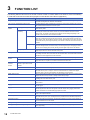
CHAPTER 1
PART NAMES
14
CHAPTER 2
SPECIFICATIONS
16
2.1
Performance Specifications . . . . . . . . . . . . . . . . . . . . . . . . . . . . . . . . . . . . . . . . . . . . . . . . . . . . . . . . . . . . . . . 16
CHAPTER 3
FUNCTION LIST
18
CHAPTER 4
PROCEDURES BEFORE OPERATION
20
CHAPTER 5
WIRING
22
5.1
CONTENTS
TERMS . . . . . . . . . . . . . . . . . . . . . . . . . . . . . . . . . . . . . . . . . . . . . . . . . . . . . . . . . . . . . . . . . . . . . . . . . . . . . . . . .12
Wiring Precautions . . . . . . . . . . . . . . . . . . . . . . . . . . . . . . . . . . . . . . . . . . . . . . . . . . . . . . . . . . . . . . . . . . . . . . 22
Connectors for external devices . . . . . . . . . . . . . . . . . . . . . . . . . . . . . . . . . . . . . . . . . . . . . . . . . . . . . . . . . . . . . 22
5.2
External Wiring . . . . . . . . . . . . . . . . . . . . . . . . . . . . . . . . . . . . . . . . . . . . . . . . . . . . . . . . . . . . . . . . . . . . . . . . . 23
Signal layout of the connector for external devices . . . . . . . . . . . . . . . . . . . . . . . . . . . . . . . . . . . . . . . . . . . . . . . 23
CHAPTER 6
OPERATION EXAMPLES
26
6.1
Programming Procedure . . . . . . . . . . . . . . . . . . . . . . . . . . . . . . . . . . . . . . . . . . . . . . . . . . . . . . . . . . . . . . . . . 26
6.2
Program Examples . . . . . . . . . . . . . . . . . . . . . . . . . . . . . . . . . . . . . . . . . . . . . . . . . . . . . . . . . . . . . . . . . . . . . . 26
CHAPTER 7
7.1
OFFSET/GAIN SETTING
32
Setting Procedure . . . . . . . . . . . . . . . . . . . . . . . . . . . . . . . . . . . . . . . . . . . . . . . . . . . . . . . . . . . . . . . . . . . . . . . 32
APPENDICES
36
Appendix 1 I/O Conversion Characteristics . . . . . . . . . . . . . . . . . . . . . . . . . . . . . . . . . . . . . . . . . . . . . . . . . . . . . . . 36
Appendix 2 Accuracy. . . . . . . . . . . . . . . . . . . . . . . . . . . . . . . . . . . . . . . . . . . . . . . . . . . . . . . . . . . . . . . . . . . . . . . . . . 41
Appendix 3 External Dimensions . . . . . . . . . . . . . . . . . . . . . . . . . . . . . . . . . . . . . . . . . . . . . . . . . . . . . . . . . . . . . . . . 42
INDEX
44
REVISIONS . . . . . . . . . . . . . . . . . . . . . . . . . . . . . . . . . . . . . . . . . . . . . . . . . . . . . . . . . . . . . . . . . . . . . . . . . . . . . .46
WARRANTY . . . . . . . . . . . . . . . . . . . . . . . . . . . . . . . . . . . . . . . . . . . . . . . . . . . . . . . . . . . . . . . . . . . . . . . . . . . . .47
TRADEMARKS . . . . . . . . . . . . . . . . . . . . . . . . . . . . . . . . . . . . . . . . . . . . . . . . . . . . . . . . . . . . . . . . . . . . . . . . . . .48
11
RELEVANT MANUALS
Manual name [manual number]
Description
Available form
MELSEC iQ-R Channel Isolated Analog-Digital Converter Module
User's Manual (Startup)
[SH-081485ENG] (this manual)
Performance specifications, procedures before operation,
wiring, operation examples, and offset/gain setting of the A/D
converter module
Print book
MELSEC iQ-R Channel Isolated Analog-Digital Converter Module
User's Manual (Application)
[SH-081487ENG]
Functions, parameter settings, troubleshooting, I/O signals,
and buffer memory of the A/D converter module
Print book
MELSEC iQ-R Programming Manual (Instructions, Standard
Functions/Function Blocks)
[SH-081266ENG]
Instructions for the CPU module, dedicated instructions for
the intelligent function modules, and standard functions/
function blocks
e-Manual
EPUB
PDF
e-Manual
EPUB
PDF
e-Manual
EPUB
PDF
This manual does not include detailed information on the following:
• General specifications
• Applicable CPU modules and the number of mountable modules
• Installation
For details, refer to the following.
MELSEC iQ-R Module Configuration Manual
This manual does not include information on the module function blocks.
For details, refer to the Function Block Reference for the module used.
e-Manual refers to the Mitsubishi FA electronic book manuals that can be browsed using a dedicated tool.
e-Manual has the following features:
• Required information can be cross-searched in multiple manuals.
• Other manuals can be accessed from the links in the manual.
• The hardware specifications of each part can be found from the product figures.
• Pages that users often browse can be bookmarked.
TERMS
Unless otherwise specified, this manual uses the following terms.
12
Term
Description
A/D converter module
The abbreviation for the MELSEC iQ-R series channel isolated analog-digital converter module
GX Works3
The product name of the software package for the MELSEC programmable controllers
Q compatible mode
A mode in which the module operates with the buffer memory map converted to the equivalent one of the
MELSEC Q series
R mode
A mode in which the module operates with the buffer memory map that has been newly laid out in the MELSEC
iQ-R series
Watchdog timer error
An error that occurs if the internal processing of the A/D converter module fails. The module monitors its own
internal processing by using the watchdog timer.
Engineering tool
Another term for GX Works3
Offset/gain setting mode
A mode used for the offset/gain setting
Global label
A label that is valid for all the program data when multiple program data are created in the project. There are two
types of global label: a module specific label (module label), which is generated automatically by GX Works3,
and an optional label, which can be created for any specified device.
Factory default setting
A generic term for analog input ranges of 0 to 10V, 0 to 5V, 1 to 5V, -10 to 10V, 0 to 20mA, 4 to 20mA, 1 to 5V
(extended mode), and 4 to 20mA (extended mode).
In the window on the engineering tool, 4 to 20mA (extended mode) and 1 to 5V (extended mode) are displayed
as the following:
• 4 to 20mA (Extension)
• 1 to 5V (Extension)
Normal mode
A mode used for normal A/D conversion.
In the engineering tool, the item name of the mode is displayed as "Normal mode (A/D conversion process)".
Term
Description
Buffer memory
A memory in an intelligent module for storing data (such as setting values and monitored values) to be
transferred to the CPU module
User range
An analog input range where any value can be set. This range can be set in the offset/gain setting.
Module label
A label that represents one of memory areas (I/O signals and buffer memory areas) specific to each module in a
given character string. For the module used, GX Works3 automatically generates this label, which can be used
as a global label.
13
1
PART NAMES
This chapter describes the part names of the A/D converter module.
(2)
(1)
(3)
(4)
(5)
No.
Name
Description
(1)
RUN LED
Indicates the operating status of the module.
On: Normal operation
Flashing (cycle of 1s): In offset/gain setting mode
Flashing (cycle of 400ms): Selected as a module for the online module change
Off: 5V power supply interrupted, watchdog timer error occurred, or module change permitted in the process
of online module change
(2)
ERR LED
Indicates the error status of the module.*1
On: Error occurred
Off: Normal operation
(3)
ALM LED
Indicates the alarm status of the module.*1
On: Alert (process alarm or rate alarm) issued
Flashing: Input signal error detected
Off: Normal operation
(4)
Connector for external devices
Connector for connection to input signal wires from external devices and others
For the signal layout, refer to the following.
Page 23 Signal layout of the connector for external devices
(5)
Production information marking
Shows the product information (16 digits) of the module.
*1
14
For details, refer to the following.
MELSEC iQ-R Channel Isolated Analog-Digital Converter Module User's Manual (Application)
1 PART NAMES
MEMO
1
1 PART NAMES
15
2
SPECIFICATIONS
This chapter describes the performance specifications.
2.1
Performance Specifications
This section describes the performance specifications of the A/D converter modules.
R60AD8-G, R60AD16-G
Item
Specifications
Number of analog input channels
Analog input voltage
• R60AD8-G: 8 channels
• R60AD16-G: 16 channels
-10 to 10VDC (input resistance 1M)
Analog input current
0 to 20mADC (input resistance 250)
Digital output value
16-bit signed binary value (-32768 to 32767)
I/O conversion characteristics, resolution*1
Analog input range
Digital output value
Voltage
0 to 32000
0 to 10V
0 to 5V
125.0V
1 to 5V (extended mode)
-8000 to 32767
(-8000 to 36000)*10
-10 to 10V
-32000 to 32000
125.0V
312.5V
29.2V*9
User range setting
0 to 20mA
312.5V
156.3V
1 to 5V
Current
Resolution
0 to 32000
4 to 20mA
625.0nA
500.0nA
4 to 20mA (extended
mode)
-8000 to 32767
(-8000 to 36000)*10
500.0nA
User range setting
-32000 to 32000
115.5nA*9
*3
Accuracy (accuracy for the maximum digital
output value)*2
Reference accuracy: Within 0.1% (32 digits)
Temperature coefficient: 35ppm/ (0.0035%/)*4
Common mode characteristics
Common mode voltage between input and common ground (input voltage 0V): 500VAC
Common mode voltage rejection ratio (VCM < 500V): 60Hz 107dB, 50Hz 106dB
Conversion speed*5
Response
10ms/CH
time*6
20ms
Absolute maximum input
Voltage: 15V, Current: 30mA*7
Number of offset/gain settings*8
50000 times maximum
Isolation method
Between I/O terminals and programmable controller power supply: Transformer
Between analog input channels: Transformer
Withstand voltage
Between I/O terminals and programmable controller power supply: 500VACrms for 1 minute
Between analog input channels: 1000VACrms for 1 minute
Insulation resistance
Between I/O terminals and programmable controller power supply: 10M or higher, at 500VDC
Between analog input channels: 10M or higher, at 500VDC
Number of occupied I/O points
External interface
Applicable wire size
40-pin connector
When A6CON1 and
A6CON4 are used
When A6CON2 is used
Connector for external devices
Internal current consumption (5VDC)
External
dimensions
Height
Width
Depth
16
• R60AD8-G: 16 points, 1 slot (I/O assignment: Intelligent 16 points)
• R60AD16-G: 32 points, 2 slots (I/O assignment: Empty 16 points + Intelligent 16 points)
2 SPECIFICATIONS
2.1 Performance Specifications
0.088 to 0.3 (28 to 22 AWG) (stranded wire)
0.088 to 0.24 (28 to 24 AWG) (stranded wire)
A6CON1, A6CON2, A6CON4 (sold separately)
• R60AD8-G: 0.33A
• R60AD16-G: 0.52A
106mm (Base unit mounting side: 98mm)
• R60AD8-G: 27.8mm
• R60AD16-G: 56mm
110mm
Item
Weight
Specifications
• R60AD8-G: 0.19kg
• R60AD16-G: 0.26kg
*1
For details on the I/O conversion characteristics, refer to the following.
Page 36 I/O Conversion Characteristics
*2 Except for the conditions under noise influence.
*3 The accuracy at an ambient temperature when the offset/gain setting is configured.
*4 The accuracy based on a temperature change of 1.
*5 The period at which the digital output value is updated.
*6 The time taken for an analog input signal to arrive at the A/D converter inside the module.
*7 These voltage and current values are instantaneous values at which no breakdown occurs in the internal resistance of the module.
*8 A count more than 50000 times causes Number of writes to offset/gain settings reach limit error (error code: 1080H).
*9 Maximum resolution in the user range setting.
*10 The range of data that is stored in Digital output value (32 bits).
2
Restrictions
The module R60AD16-G takes up two slots and so there are restrictions on the available firmware version of the RCPU
module. For details, refer to the following.
• MELSEC iQ-R CPU Module User's Manual (Application)
2 SPECIFICATIONS
2.1 Performance Specifications
17
3
FUNCTION LIST
The following table lists the functions of the A/D converter module. For further details on the functions, refer to the following.
MELSEC iQ-R Channel Isolated Analog-Digital Converter Module User's Manual (Application)
Item
Description
Range switching function
Allows the input range of analog input to be switched for each channel. Switching the range makes
it possible to change the I/O conversion characteristics.
A/D conversion enable/disable setting function
Controls whether to enable or disable A/D conversion for each channel. Disabling A/D conversion
for unused channels reduces the conversion cycles.
A/D conversion
method
Sampling processing
Converts analog input values into digital output values at every sampling period, storing them in
buffer memory areas.
Averaging
processing
Time average
Executes A/D conversion for the set time and performs the averaging processing on the total value
excluding the maximum and minimum values. The processed values are stored in the buffer
memory area. The number of processing times within the set time changes depending on the
number of channels where A/D conversion is enabled.
Count average
Executes A/D conversion for a set number of times and performs the averaging processing on the
total value excluding the maximum and minimum values. The processed values are stored in the
buffer memory area. The time taken to store the average value obtained by the average processing
in the buffer memory area changes depending on the number of channels where A/D conversion is
enabled.
Moving average
Averages digital output values taken at every sampling period for a specified number of times, and
stores the averaged value in the buffer memory area. The target range for averaging processing
moves at each sampling period, thereby allowing the latest digital output value to be obtained.
Primary delay filter
Scaling function
18
Smooths the transient noise of analog input depending on the set time constant. The smoothed
digital output values are stored in the buffer memory area.
Performs scale conversion on digital output values within the range from a scaling upper limit value
to a scaling lower limit value, both of which are set at desired values. This function reduces the time
and effort to create a program of the scale conversion.
Alert output
function
Process alarm
Outputs an alert when a digital operation value falls within the preset alert output range.
Rate alarm
Outputs an alert if the change rate of a digital output value is equal to or more than the rate alarm
upper limit value, or is equal to or less than the rate alarm lower limit value.
Input signal error
detection
function
Upper limit detection, lower limit
detection, upper and lower limit
detection
Outputs an alarm when an analog input value exceeds the preset range.
Simple disconnection detection
Outputs an alarm when an analog input value is 0.5V or smaller or 2mA or smaller.
Shift function
Adds (shifts) a set conversion value shift amount to a digital output value, and stores the result in
the buffer memory area. A change in conversion value shift amount is reflected to the digital
operation value in real time, which facilitates fine adjustment at system start-up.
Digital clipping function
Fixes a possible digital operation value to the maximum digital output value or the minimum digital
output value when an input current or voltage exceeds the input range.
Difference conversion function
Subtracts a difference conversion reference value from a digital operation value and stores the
resulting value in the buffer memory area.
Maximum value/minimum value hold function
Stores the maximum and minimum values of digital operation values in the buffer memory area for
each channel.
Logging function
Logs (records) digital output values or digital operation values. For each channel, 1000 points data
can be logged.
Logging read function
Makes it possible to store more than 1000 points of logging data without stopping logging by
transferring the device data to the file register of the CPU module during logging. This function
reduces the takt time in a test demanding high-speed conversion.
Interrupt function
Executes an interrupt program of the CPU module when an interrupt factor such as an input signal
error or alert output is detected.
Error history function
Records errors and alarms that have occurred in the A/D converter module, storing the record into
the buffer memory area. Up to 16 storage areas are provided for errors and alarms, respectively.
Event history function
Collects generated errors and alarms, and performed operations in the A/D converter module as
event information into the CPU module.
Offset/gain setting
Allows the correction of errors in digital output values.
Backing up, saving, and restoring offset/gain values
The A/D converter module is capable of backing up, saving, and restoring offset/gain values of the
user range setting.
3 FUNCTION LIST
Item
Description
Online module change
Allows module change without stopping the system. For the procedure of the online module
change, refer to the following.
MELSEC iQ-R Online Module Change Manual
Q compatible mode function
Allows the buffer memory addresses of the A/D converter module to be the same layout as the
MELSEC-Q series module.
This compatibility makes it possible to reuse sequence programs that have exhibited high
performance on the MELSEC-Q series modules.
3
3 FUNCTION LIST
19
4
PROCEDURES BEFORE OPERATION
This chapter describes the procedures before operation.
1.
Mounting a module
Mount the A/D converter module in any desired configuration.
Page 26 System configuration
2.
Wiring
Perform wiring of external devices to the A/D converter module.
Page 23 External Wiring
3.
Adding a module
Add the A/D converter module to a module configuration by using the engineering tool. For details, refer to the following.
GX Works3 Operating Manual
4.
Parameter settings
Set up the parameters of the A/D converter module by using the engineering tool. For details, refer to the following.
MELSEC iQ-R Channel Isolated Analog-Digital Converter Module User's Manual (Application)
5.
Offset/gain setting
Perform the offset/gain setting to set a user range, if necessary.
Page 32 OFFSET/GAIN SETTING
6.
Programming
Create a program. For details, refer to the following.
Page 26 OPERATION EXAMPLES
20
4 PROCEDURES BEFORE OPERATION
MEMO
4
4 PROCEDURES BEFORE OPERATION
21
5
WIRING
This chapter describes the wiring of the A/D converter module.
5.1
Wiring Precautions
• Check the signal layout before wiring to the A/D converter module, and connect the cables correctly. For the signal layout,
refer to the following.
Page 23 Signal layout of the connector for external devices
• Provide a single-point ground for the shield wire and the shield of the shielded cable.
Connectors for external devices
Precautions
Tighten the connector screws within the specified torque range.
Screw type
Tightening torque range
Connector screw (M2.6)
0.20 to 0.29Nm
• Use copper wire with a temperature rating of 75 or higher for the connector.
• Use UL listed connectors if necessary for UL compliance.
Applicable connectors
Connectors for external devices to be used for the A/D converter module are sold separately.
The following tables list the applicable connectors, and the reference product of a crimping tool
■40-pin connectors
Type
Model
Applicable wire size
*1
Soldering type connector (straight type)
A6CON1
0.088 to 0.3 (28 to 22 AWG) (stranded wire)
Crimping type connector (straight type)
A6CON2
0.088 to 0.24 (28 to 24 AWG) (stranded wire)
Soldering type connector (dual purpose (straight/oblique) type)
A6CON4*1
0.088 to 0.3 (28 to 22 AWG) (stranded wire)
*1
Select wires with a sheath outside diameter of 1.3mm or shorter when using 40 wires.
Select wires suitable to the current value used.
• The A6CON3 (IDC type connector (straight type)) cannot be used.
• The connector/terminal block converter module and the dedicated cables that are designed for the
MELSEC-Q series channel isolated analog module can be used. For details, refer to the following.
Page 25 When the connector/terminal block converter module is used
■40-pin connector crimping tool
Type
Model
Contact
Crimping tool
FCN-363T-T005/H
FUJITSU COMPONENT LIMITED
For how to wire the connector and how to use the crimping tool, contact the manufacturer.
Wiring method, connection procedure, and disconnection procedure of the connector
For the wiring method, connection procedure, and disconnection procedure, refer to the following.
MELSEC iQ-R Module Configuration Manual
22
5 WIRING
5.1 Wiring Precautions
5.2
External Wiring
Signal layout of the connector for external devices
The following shows the signal layout of the connector for external devices for the A/D converter module.
• R60AD8-G
Pin layout (viewed from the front of the
module)
A1
A2
A3
A4
A5
A6
A7
A8
A9
A10
A11
A12
A13
A14
A15
A16
A17
A18
A19
A20
B1
B2
B3
B4
B5
B6
B7
B8
B9
B10
B11
B12
B13
B14
B15
B16
B17
B18
B19
B20
Viewed from the front of the module
Pin number
Signal name
Pin number
Signal name
A1
CH1 V+
B1
CH1 V-/I-
A2
CH1 I+
B2
A3
B3
CH2 V+
A4
CH2 V-/I-
B4
CH2 I+
A5
B5
A6
CH3 V+
B6
CH3 V-/I-
A7
CH3 I+
B7
A8
B8
CH4 V+
A9
CH4 V-/I-
B9
CH4 I+
A10
B10
A11
CH5 V+
B11
CH5 V-/I-
A12
CH5 I+
B12
A13
B13
CH6 V+
A14
CH6 V-/I-
B14
CH6 I+
A15
B15
A16
CH7 V+
B16
CH7 V-/I-
A17
CH7 I+
B17
A18
B18
CH8 V+
A19
CH8 V-/I-
B19
CH8 I+
A20
B20
5
• R60AD16-G
Pin layout (viewed from the front of the
module)
2A1
2A2
2A3
2A4
2A5
2A6
2A7
2A8
2A9
2A10
2A11
2A12
2A13
2A14
2A15
2A16
2A17
2A18
2A19
2A20
2B1
2B2
2B3
2B4
2B5
2B6
2B7
2B8
2B9
2B10
2B11
2B12
2B13
2B14
2B15
2B16
2B17
2B18
2B19
2B20
2A1 to 2B20
1A1
1A2
1A3
1A4
1A5
1A6
1A7
1A8
1A9
1A10
1A11
1A12
1A13
1A14
1A15
1A16
1A17
1A18
1A19
1A20
1B1
1B2
1B3
1B4
1B5
1B6
1B7
1B8
1B9
1B10
1B11
1B12
1B13
1B14
1B15
1B16
1B17
1B18
1B19
1B20
1A1 to 1B20
Viewed from the front of the module
Pin
number
Signal
name
Pin
number
Signal
name
Pin
number
Signal
name
Pin
number
Signal
name
2A1
CH9 V+
2B1
CH9 V-/I-
1A1
CH1 V+
1B1
CH1 V-/I-
2A2
CH9 I+
2B2
1A2
CH1 I+
1B2
2A3
2B3
CH10 V+
1A3
1B3
CH2 V+
2A4
CH10 V-/I-
2B4
CH10 I+
1A4
CH2 V-/I-
1B4
CH2 I+
2A5
2B5
1A5
1B5
2A6
CH11 V+
2B6
CH11 V-/I-
1A6
CH3 V+
1B6
CH3 V-/I-
2A7
CH11 I+
2B7
1A7
CH3 I+
1B7
2A8
2B8
CH12 V+
1A8
1B8
CH4 V+
2A9
CH12 V-/I-
2B9
CH12 I+
1A9
CH4 V-/I-
1B9
CH4 I+
2A10
2B10
1A10
1B10
2A11
CH13 V+
2B11
CH13 V-/I-
1A11
CH5 V+
1B11
CH5 V-/I-
2A12
CH13 I+
2B12
1A12
CH5 I+
1B12
2A13
2B13
CH14 V+
1A13
1B13
CH6 V+
2A14
CH14 V-/I-
2B14
CH14 I+
1A14
CH6 V-/I-
1B14
CH6 I+
2A15
2B15
1A15
1B15
2A16
CH15 V+
2B16
CH15 V-/I-
1A16
CH7 V+
1B16
CH7 V-/I-
2A17
CH15 I+
2B17
1A17
CH7 I+
1B17
2A18
2B18
CH16 V+
1A18
1B18
CH8 V+
2A19
CH16 V-/I-
2B19
CH16 I+
1A19
CH8 V-/I-
1B19
CH8 I+
2A20
2B20
1A20
1B20
5 WIRING
5.2 External Wiring
23
Examples of external wiring
Here are the examples of external wiring.
■R60AD8-G, R60AD16-G
For voltage input
Signal source: 0 to ±10V
*1
A/D conversion circuit
V+
I+
V-/IShield
*4
For current input
*2
Signal source: 0 to 20mA
*3
A/D conversion circuit
V+
*1
I+
250Ω
V-/IShield
*4
*1
*2
*3
*4
For the wire, use the 2-core twisted cable.
The value indicates the input resistance of the A/D converter module.
For the current input, be sure to connect the terminals (V+) and (I+).
The connection between the terminal (V+) and the terminal (I+) should be made inside the connector for external devices (A6CON4) to
reduce the resistance of the connecting conductor.
Be sure to ground the shield wire of cables on each channel.
Ground the FG terminal of the power supply module.
24
5 WIRING
5.2 External Wiring
When the connector/terminal block converter module is used
The A/D converter module allows the use of the connector/terminal block converter module and the dedicated cables that are
designed for the Q68AD-G.
To use the connector/terminal block converter module, wire the module as shown below.
Connector/terminal block
converter module
CH1 V+
CH1 V-
*1
Dedicated cable
5
Shield*1
*1
Be sure to use a shielded cable. The shield must be grounded.
Product name
Model
Remarks
Contact
Connector/terminal block converter module
Dedicated cable
FA-LTB40ADGN
FA-CBL05Q68ADGN
Cable length 0.5m
Your local Mitsubishi Electric sales office or
representative
FA-CBL10Q68ADGN
Cable length 1.0m
FA-CBL20Q68ADGN
Cable length 2.0m
FA-CBL30Q68ADGN
Cable length 3.0m
In the factory default settings of the modules, or the R60AD8-G and R60AD16-G, the offset/gain setting is
configured with the module being independent.
For this reason, the use of the connector/terminal block converter module and the dedicated cables may
cause an error in conversion characteristics due to the effect of conductor resistance and other factors.
If this effect is a problem, use the user range setting to set the offset and gain values.
For the offset/gain setting, refer to the following.
Page 32 OFFSET/GAIN SETTING
5 WIRING
5.2 External Wiring
25
6
OPERATION EXAMPLES
This chapter describes the programming procedure and the basic program of the A/D converter module.
6.1
Programming Procedure
Take the following steps to create a program for running the A/D converter module:
1.
Set parameters.
Page 27 Parameter settings
2.
Create a program.
Page 29 Program examples
Using function blocks (FBs) reduces load at programming and improves the readability of programs. For
details on the function blocks, refer to the following.
MELSEC iQ-R Analog-Digital Converter Module/Digital-Analog Converter Module Function Block
Reference
6.2
Program Examples
System configuration
The following figure is an example of the system configuration.
(1)
(1) Power supply module (R61P)
(2) CPU module (R120CPU)
(3) A/D converter module (R60AD8-G)
(4) Input module (RX10)
26
6 OPERATION EXAMPLES
6.1 Programming Procedure
(2)
(3)
(4)
Conditions in the program
This program reads digital output values from the A/D converter module's CH1, CH3, CH5, and CH7 where A/D conversion is
enabled.
The A/D conversion takes place in CH1 and CH7 by means of sampling processing; in CH3 by means of averaging
processing for 50 samples; and in CH5 by means of moving average for 10 samples.
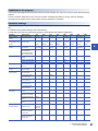
Parameter settings
Perform initial settings in the parameter settings of the engineering tool. The auto refresh setting does not need to be changed
here.
For details on the parameter settings, refer to the following.
MELSEC iQ-R Channel Isolated Analog-Digital Converter Module User's Manual (Application)
Function
Setting item
CH1
CH2
CH3
CH4
CH5
CH6
CH7
CH8
Range switching
function
Input range setting
0 to 10V
0 to 10V
4 to 20mA
4 to 20mA
A/D conversion
enable/disable setting
function
A/D conversion enable/
disable setting
A/D
conversion
enable
A/D
conversion
disable
A/D
conversion
enable
A/D
conversion
disable
A/D
conversion
enable
A/D
conversion
disable
A/D
conversion
enable
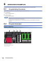
A/D
conversion
disable
A/D conversion
method
Averaging process
specification
Sampling
processing
Count
average
Moving
average
Sampling
processing
Time average/Count
average/Moving
average/Primary delay
filter constant setting
50
10
Scaling enable/disable
setting
Disable
Disable
Enable
Disable
Scaling upper limit value
16000
Scaling lower limit value
2000
Shift function
Conversion value shift
amount
0
0
2000
0
Digital clipping
function
Digital clipping enable/
disable setting
Disable
Disable
Enable
Disable
Alert output function
(process alarm)
Alert output setting
(process alarm)
Disable
Enable
Disable
Disable
Process alarm upper
upper limit value
32000
Process alarm upper
lower limit value
28000
Process alarm lower
upper limit value
4000
Process alarm lower
lower limit value
0
Alert output setting (rate
alarm)
Enable
Disable
Disable
Disable
Rate alarm alert
detection cycle setting
400 times
Rate alarm upper limit
value
25.0%
Rate alarm lower limit
value
-50.0%
Input signal error
detection setting
Upper/
lower limit
detection
Disable
Disable
Disable
Input signal error
detection upper limit
setting value
8.0%
Input signal error
detection lower limit
setting value
8.0%
Scaling function
Alert output function
(rate alarm)
Input signal error
detection function
6 OPERATION EXAMPLES
6.2 Program Examples
6
27
Label settings
GX Works3 provides functions that support the creation of a program.
The following table lists the module labels and global labels used for the program examples in this section.
There is no need to change the settings of the module labels. For details on the global labels, refer to the following.
MELSEC iQ-R Programming Manual (Program Design)
Classification
Label name
Description
Device
Module label
R60ADG_1.bModuleREADY
Module READY
X0
R60ADG_1.bInputSignalErrorDetectionSignal
Input signal error detection signal
X0C
R60ADG_1.bMaxValueMinValueResetCompletedFlag
Maximum value/minimum value reset
completed flag
X0D
Labels to be defined
28
R60ADG_1.bA_D_conversionCompletedFlag
A/D conversion completed flag
X0E
R60ADG_1.bErrorFlag
Error flag
X0F
R60ADG_1.bOperatingConditionSettingRequest
Operating condition setting request
Y9
R60ADG_1.bMaxValueMinValueResetRequest
Maximum value/minimum value reset request
Y0D
R60ADG_1.uA_D_conversionCompletedFlag.0
A/D conversion completed flag
R60ADG_1.stnMonitor[0].wDigitalOutputValue
CH1 Digital output value
R60ADG_1.uA_D_conversionCompletedFlag.2
A/D conversion completed flag
R60ADG_1.stnMonitor[2].wDigitalOutputValue
CH3 Digital output value
R60ADG_1.uA_D_conversionCompletedFlag.4
A/D conversion completed flag
R60ADG_1.stnMonitor[4].wDigitalOperationValue
CH5 Digital operation value
R60ADG_1.uA_D_conversionCompletedFlag.6
A/D conversion completed flag
R60ADG_1.stnMonitor[6].wDigitalOutputValue
CH7 Digital output value
R60ADG_1.stnMonitor[4].wMaxValue
CH5 Maximum value
R60ADG_1.stnMonitor[4].wMinValue
CH5 Minimum value
R60ADG_1.uWarningOutputFlagProcessAlarmUpperLimit.2
Alert output flag (process alarm upper limit)
R60ADG_1.uWarningOutputFlagProcessAlarmLowerLimit.2
Alert output flag (process alarm lower limit)
R60ADG_1.uWarningOutputFlagRateAlarmUpperLimit.0
Alert output flag (rate alarm upper limit)
R60ADG_1.uWarningOutputFlagRateAlarmLowerLimit.0
Alert output flag (rate alarm lower limit)
R60ADG_1.uInputSignalErrorDetectionFlag.0
Input signal error detection flag
Define global labels as shown below:
6 OPERATION EXAMPLES
6.2 Program Examples
Program examples
■Program example 1
• This program is an example to read and save the digital output values of CH1, CH3, and CH7, and the digital operation
value of CH5.
6
(0)
CH1 Digital output value, CH3 Digital output value, CH5 Digital operation value, and CH7 Digital output value are to be read.
■Program example 2
• This program is an example to read the maximum and minimum values of CH5, which in turn are cleared.
(0)
CH5 Maximum value and CH5 Minimum value are to be read.
(12)
'Maximum value/minimum value reset request' (YD) is to be turned on.
(15)
'Maximum value/minimum value reset request' (YD) is to be turned off.
6 OPERATION EXAMPLES
6.2 Program Examples
29
■Program example 3
• This program is an example to perform the processing at the time when a process alarm upper/lower limit alert is issued in
CH3.
(0)
The processing at the time when a process alarm upper limit alert is issued in CH3 is to be performed.
(6)
The processing at the time when a process alarm lower limit alert is issued in CH3 is to be performed.
■Program example 4
• This program is an example to perform the processing at the time when a rate alarm upper/lower limit alert is issued in
CH1.
30
(0)
The processing at the time when a rate alarm upper limit alert is issued in CH1 is to be performed.
(6)
The processing at the time when a rate alarm lower limit alert is issued in CH1 is to be performed.
6 OPERATION EXAMPLES
6.2 Program Examples
■Program example 5
• This program is an example where after the processing of an input signal error of CH1, the input signal error detection flag
and the stored error code are cleared.
6
(0)
The processing at the time when an input signal error is detected in CH1 is to be performed.
(6)
Error manipulation start flag is to be turned on.
6 OPERATION EXAMPLES
6.2 Program Examples
31
7
OFFSET/GAIN SETTING
Using the user range setting requires the offset/gain setting.
Access to the offset/gain setting window in the engineering tool to set the offset and gain values.
7.1
Setting Procedure
The setting procedure for the offset/gain setting of the A/D converter module is as follows:
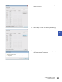
[Tool] [Module Tool List]
1.
In "Analog Input", select "Offset/gain Setting" and click
the [OK] button.
2.
Select the target module for the offset/gain setting, and
click the [OK] button.
3.
32
7 OFFSET/GAIN SETTING
7.1 Setting Procedure
Click the [Yes] button.
4.
Mark the checkbox of the channel where offset and gain
values are to be set.
5.
Select voltage or current and click the [Offset Setting]
button.
7
6.
Apply the offset voltage or current to the corresponding
channel, and click the [Yes] button.
7 OFFSET/GAIN SETTING
7.1 Setting Procedure
33
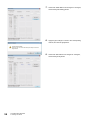
7.
Check that "Offset Status" has changed to "Changed",
and click the [Gain Setting] button.
8.
Apply the gain voltage or current to the corresponding
channel, and click the [Yes] button.
9.
Check that "Gain Status" has changed to "Changed",
and click the [Close] button.
34
7 OFFSET/GAIN SETTING
7.1 Setting Procedure
10. Click the [Yes] button.
7
7 OFFSET/GAIN SETTING
7.1 Setting Procedure
35
APPENDICES
Appendix 1
I/O Conversion Characteristics
The I/O conversion characteristics of A/D conversion are expressed by the slope of the straight line connecting the offset
value and the gain value, both of which are used when an analog signal (voltage or current) from outside the programmable
controller is converted to the corresponding digital value.
Offset value
An analog input value (voltage or current) which turns 0 as a digital output value after conversion
Gain value
An analog input value (voltage or current) which turns 32000 as a digital output value after conversion
36
APPENDICES
Appendix 1 I/O Conversion Characteristics
Voltage input characteristics
A
The following shows the list of analog input ranges at the voltage input and the graphs of each of the voltage input
characteristics.
Practical analog input range
32767
32000
(2)
(3) (4)
Digital
output
0
value -768
-32000
-32768
-15
(1)
1
-10
-5
0
5
10
15
Analog input voltage (V)
Practical analog
input range
Practical analog
input range
36767
36000
32767
32000
Digital
output
value
32000
(5) (for 16 bits)
0
-8000
-8768
-32000
-32768
-15
(5) (for 32 bits)
Digital
output
value
1
0
1
-8000
-8768
-10
-5
0
5.5
5.096
5
10
15
-32000
-32768
-15
-10
Analog input voltage (V)
-5
0
5
5.5
10
15
Analog input voltage (V)
No.
Input range setting
Offset value
Gain value
Digital output value*3
Resolution
(1)
1 to 5V
1V
5V
0 to 32000
125.0V
(2)
0 to 5V
0V
5V
(3)
-10 to 10V
0V
10V
-32000 to 32000
(4)
0 to 10V
0V
10V
0 to 32000
156.3V
312.5V
(5)
1 to 5V (extended mode)
1V
5V
-8000 to 36000
125.0V
User range setting
*1
*1
-32000 to 32000
29.2V*2
APPENDICES
Appendix 1 I/O Conversion Characteristics
37
*1
*2
*3
Set the offset value and gain value in the user range setting within a range satisfying the following conditions. Failure to satisfy the
conditions may not result in proper A/D conversion.
Setting range of the offset value and gain value: -10 to 10V
((Gain value) - (Offset value)) 1.6V
Maximum resolution in the user range setting.
If an analog input value exceeds the range of digital output value, the digital output value is fixed to the maximum or minimum value.
Input range setting
Digital output value
Minimum
Maximum
1 to 5V
-768
32767
0 to 5V
-10 to 10V
-32768
0 to 10V
-768
1 to 5V (extended mode)
-8768
36767
User range setting
-32768
32767
• Set values within the practical range of the analog input and the digital output at each input range. If the
range is exceeded, the resolution and accuracy may not fall within the range of the performance
specifications. (Do not use the values in the dotted line region in the graph of voltage input characteristics.)
• Do not set the voltage over 15V. Doing so can cause breakdown of the elements.
38
APPENDICES
Appendix 1 I/O Conversion Characteristics
Current input characteristics
A
The following shows the list of analog input ranges at the current input and the graphs of each of the current input
characteristics.
Practical analog
input range
32767
32000
(2)
Digital
output
value
(1)
0
-768
-32000
-32768
-30
4
-20
0
20
30
Analog input current (mA)
Practical analog
input range
Practical analog
input range
36767
36000
32767
32000
Digital
output
value
32000
(3) (for 16 bits)
0
4
-8000
-8768
-32000
-32768
-30
(3) (for 32 bits)
0
4
-8000
-8768
-20
0
20
Analog input current (mA)
No.
Digital
output
value
Input range setting
30
-32000
-32768
-30
22.00
20.384
Offset value
-20
0
20
22.00
30
Analog input current (mA)
Gain value
Digital output value*3
0 to 32000
(1)
4 to 20mA
4mA
20mA
(2)
0 to 20mA
0mA
20mA
Resolution
500.0nA
625.0nA
(3)
4 to 20mA (extended mode)
4mA
20mA
-8000 to 36000
500.0nA
User range setting
*1
*1
-32000 to 32000
115.5nA*2
*1
*2
*3
Set the offset value and gain value in the user range setting within a range satisfying the following conditions. Failure to satisfy the
conditions may not result in proper A/D conversion.
Gain value 20mA, offset value 0mA
((Gain value) - (Offset value)) 12.2mA
Maximum resolution in the user range setting.
If an analog input value exceeds the range of digital output value, the digital output value is fixed to the maximum or minimum value.
APPENDICES
Appendix 1 I/O Conversion Characteristics
39
Input range setting
Digital output value
Minimum
Maximum
-768
32767
4 to 20mA (extended mode)
-8768
36767
User range setting
-32768
32767
4 to 20mA
0 to 20mA
• Set values within the practical range of the analog input and the digital output at each input range. If the
range is exceeded, the resolution and accuracy may not fall within the range of the performance
specifications. (Do not use the values in the dotted line region in the graph of current input characteristics.)
• Do not set the voltage over 30mA. Doing so can cause breakdown of the elements.
40
APPENDICES
Appendix 1 I/O Conversion Characteristics
Appendix 2
Accuracy
A
The accuracy of A/D conversion is the accuracy for the maximum value of digital output value. The accuracy is given by the
following formula:
Accuracy = (Reference accuracy) + (Temperature coefficient) (Temperature variation)
• Reference accuracy: The accuracy at an ambient temperature when the offset/gain setting is configured. (0.1% (32
digits))
• Temperature coefficient: The accuracy based on a temperature change of 1. (0.0035%/ (1.12 digits))
An output characteristic change resulting from a change in the offset/gain setting or the analog input range does not sacrifice
the reference accuracy and temperature coefficient, which are maintained within the described range of the performance
specifications
(except for the conditions under noise influence).
Ex.
Accuracy when the temperature changes by 5 from 25 to 30
(0.1%) + (0.0035%/ 5) = 0.1175% (38 digits)
32000
Voltage fluctuation range
Digital
output
value
0
-32000
-10
0
10
Analog input voltage (V)
APPENDICES
Appendix 2 Accuracy
41
Appendix 3
External Dimensions
The following figure shows the external dimensions of the A/D converter module.
98
106
4
R60AD8-G
110
27.8
(Unit: mm)
98
106
4
R60AD16-G
110
56
(Unit: mm)
42
APPENDICES
Appendix 3 External Dimensions
MEMO
A
APPENDICES
Appendix 3 External Dimensions
43
INDEX
A
Accuracy of A/D conversion . . . . . . . . . . . . . . . . 41
ALM LED . . . . . . . . . . . . . . . . . . . . . . . . . . . . . 14
C
Connector for external devices . . . . . . . . . . . . . . 22
Connector/terminal block converter module . . . . . 25
Current input characteristics . . . . . . . . . . . . . . . . 39
D
Dedicated cable . . . . . . . . . . . . . . . . . . . . . . . . 25
E
ERR LED . . . . . . . . . . . . . . . . . . . . . . . . . . . . . 14
External dimensions . . . . . . . . . . . . . . . . . . . . . 42
External wiring . . . . . . . . . . . . . . . . . . . . . . . . . 23
F
Function block (FB) . . . . . . . . . . . . . . . . . . . . . . 26
G
Gain value . . . . . . . . . . . . . . . . . . . . . . . . . . . . 36
O
Offset value . . . . . . . . . . . . . . . . . . . . . . . . . . . 36
Offset/gain setting . . . . . . . . . . . . . . . . . . . . . . . 32
P
Performance specifications . . . . . . . . . . . . . . . . 16
R
RUN LED . . . . . . . . . . . . . . . . . . . . . . . . . . . . . 14
V
Voltage input characteristics . . . . . . . . . . . . . . . . 37
44
MEMO
I
45
REVISIONS
*The manual number is given on the bottom left of the back cover.
Revision date
*Manual number
Description
January 2015
SH(NA)-081485ENG-A
First edition
Japanese manual number: SH-081484-A
This manual confers no industrial property rights of any other kind, nor does it confer any patent licenses. Mitsubishi Electric Corporation cannot be held
responsible for any problems involving industrial property rights which may occur as a result of using the contents noted in this manual.
2015 MITSUBISHI ELECTRIC CORPORATION
46
WARRANTY
Please confirm the following product warranty details before using this product.
1. Gratis Warranty Term and Gratis Warranty Range
If any faults or defects (hereinafter "Failure") found to be the responsibility of Mitsubishi occurs during use of the product
within the gratis warranty term, the product shall be repaired at no cost via the sales representative or Mitsubishi Service
Company.
However, if repairs are required onsite at domestic or overseas location, expenses to send an engineer will be solely at
the customer's discretion. Mitsubishi shall not be held responsible for any re-commissioning, maintenance, or testing
on-site that involves replacement of the failed module.
[Gratis Warranty Term]
The gratis warranty term of the product shall be for one year after the date of purchase or delivery to a designated place.
Note that after manufacture and shipment from Mitsubishi, the maximum distribution period shall be six (6) months, and
the longest gratis warranty term after manufacturing shall be eighteen (18) months. The gratis warranty term of repair
parts shall not exceed the gratis warranty term before repairs.
[Gratis Warranty Range]
(1) The range shall be limited to normal use within the usage state, usage methods and usage environment, etc., which
follow the conditions and precautions, etc., given in the instruction manual, user's manual and caution labels on the
product.
(2) Even within the gratis warranty term, repairs shall be charged for in the following cases.
1. Failure occurring from inappropriate storage or handling, carelessness or negligence by the user. Failure caused
by the user's hardware or software design.
2. Failure caused by unapproved modifications, etc., to the product by the user.
3. When the Mitsubishi product is assembled into a user's device, Failure that could have been avoided if functions
or structures, judged as necessary in the legal safety measures the user's device is subject to or as necessary by
industry standards, had been provided.
4. Failure that could have been avoided if consumable parts (battery, backlight, fuse, etc.) designated in the
instruction manual had been correctly serviced or replaced.
5. Failure caused by external irresistible forces such as fires or abnormal voltages, and Failure caused by force
majeure such as earthquakes, lightning, wind and water damage.
6. Failure caused by reasons unpredictable by scientific technology standards at time of shipment from Mitsubishi.
7. Any other failure found not to be the responsibility of Mitsubishi or that admitted not to be so by the user.
2. Onerous repair term after discontinuation of production
(1) Mitsubishi shall accept onerous product repairs for seven (7) years after production of the product is discontinued.
Discontinuation of production shall be notified with Mitsubishi Technical Bulletins, etc.
(2) Product supply (including repair parts) is not available after production is discontinued.
3. Overseas service
Overseas, repairs shall be accepted by Mitsubishi's local overseas FA Center. Note that the repair conditions at each FA
Center may differ.
4. Exclusion of loss in opportunity and secondary loss from warranty liability
Regardless of the gratis warranty term, Mitsubishi shall not be liable for compensation of damages caused by any cause
found not to be the responsibility of Mitsubishi, loss in opportunity, lost profits incurred to the user by Failures of
Mitsubishi products, special damages and secondary damages whether foreseeable or not, compensation for accidents,
and compensation for damages to products other than Mitsubishi products, replacement by the user, maintenance of
on-site equipment, start-up test run and other tasks.
5. Changes in product specifications
The specifications given in the catalogs, manuals or technical documents are subject to change without prior notice.
47
TRADEMARKS
Microsoft, Windows, Windows Vista, Windows NT, Windows XP, Windows Server, Visio, Excel, PowerPoint, Visual Basic,
Visual C++, and Access are either registered trademarks or trademarks of Microsoft Corporation in the United States, Japan,
and other countries.
Intel, Pentium, and Celeron are either registered trademarks or trademarks of Intel Corporation in the United States and other
countries.
Ethernet is a trademark of Xerox Corp.
The SD and SDHC logos are either registered trademarks or trademarks of SD-3C, LLC.
All other company names and product names used in this manual are either trademarks or registered trademarks of their
respective companies.
48
SH(NA)-081485ENG-A
SH(NA)-081485ENG-A(1501)MEE
MODEL:
R-AD-G-U-IN-E
MODEL CODE: 13JX29
HEAD OFFICE : TOKYO BUILDING, 2-7-3 MARUNOUCHI, CHIYODA-KU, TOKYO 100-8310, JAPAN
NAGOYA WORKS : 1-14 , YADA-MINAMI 5-CHOME , HIGASHI-KU, NAGOYA , JAPAN
When exported from Japan, this manual does not require application to the
Ministry of Economy, Trade and Industry for service transaction permission.
Specifications subject to change without notice.