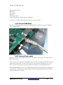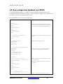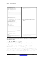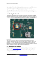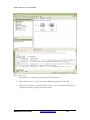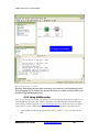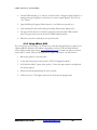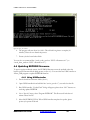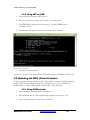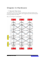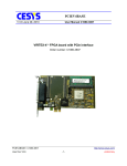
1
LOGIC Emulation Source User Manual DN9000K10 DN9000K10 User Manual Major Revision 1 Last Update April 13, 2009 7469 Draper Ave. La Jolla, CA92037 USA Phone 858.454.3419 • Fax 858.454.1728 [email protected] www.dinigroup.com DN9000K10 User Guide www.dinigroup.com 0 Table of Contents 0 TABLE OF CONTENTS.......................................................................................... 3 CHAPTER 1: INTRODUCTION .................................................................................... 1 1 MANUAL CONTENTS............................................................................................ 1 1.1 1.2 1.3 1.4 1.5 1.6 2 INTRODUCTION ........................................................................................................ 1 QUICK START GUIDE............................................................................................... 1 CONTROLLER SOFTWARE........................................................................................ 2 HARDWARE ............................................................................................................. 2 THE REFERENCE DESIGN ........................................................................................ 2 ORDERING INFORMATION ....................................................................................... 2 CONVENTIONS........................................................................................................ 2 2.1 TYPOGRAPHICAL ..................................................................................................... 2 2.2 MANUAL CONTENT ................................................................................................. 2 2.2.1 File names ......................................................................................................... 2 2.2.2 Physical Dimensions ........................................................................................ 3 2.2.3 Part Pin Names ................................................................................................. 3 2.2.4 Schematic Clippings ......................................................................................... 3 2.3 TERMINOLOGY ........................................................................................................ 3 3 RESOURCES ............................................................................................................. 4 3.1 USER CD ................................................................................................................. 4 3.2 DINIGROUP.COM ...................................................................................................... 5 3.3 ERRATA AND CUSTOMER NOTIFICATIONS.............................................................. 5 3.3.1 Existing Errata.................................................................................................. 5 3.4 SCHEMATICS AND NETLIST ..................................................................................... 6 3.4.1 Netlist................................................................................................................. 6 3.4.2 Net name conventions....................................................................................... 6 3.5 DATASHEET LIBRARY ............................................................................................. 6 3.6 XILINX ..................................................................................................................... 6 3.7 DINI GROUP REFERENCE DESIGNS ......................................................................... 7 3.8 BOARD MODELS ...................................................................................................... 7 3.8.1 Base System Builder ......................................................................................... 7 3.8.2 Using Partitioning and 3rd party synthesis tools ............................................. 7 4 EMAIL AND PHONE SUPPORT .......................................................................... 7 CHAPTER 2: QUICK START GUIDE ......................................................................... 9 1 PROVIDED MATERIALS ...................................................................................... 9 1.1 2 SYSTEM REQUIREMENTS ......................................................................................... 9 WARNINGS .............................................................................................................10 DN9000K10 User Guide www.dinigroup.com T A B L E 2.1 2.2 2.3 3 O F C O N T E N T S ESD .......................................................................................................................10 OTHER ...................................................................................................................10 OTHER WARNINGS .................................................................................................11 PRE-POWER ON INSTRUCTIONS ...................................................................11 3.1 3.2 3.3 INSTALL MEMORY.................................................................................................12 PREPARE CONFIGURATION FILES ...........................................................................13 INSERT THE COMPACT FLASH CARD INTO THE DN9000K10’S COMPACT FLASH SLOT 13 3.4 CABLES ..................................................................................................................13 3.4.1 Connect RS232 Cable.....................................................................................13 3.4.2 Connect USB Cable ........................................................................................14 3.4.3 Connect Power cable......................................................................................14 3.5 VIEW CONFIGURATION FEEDBACK OVER RS232 ..................................................15 3.6 CHECK LED STATUS LIGHTS .................................................................................16 4 RUN USB CONTROLLER....................................................................................19 4.1 DRIVER INSTALLATION .........................................................................................19 4.2 OPERATING THE USB CONTROLLER PROGRAM ...................................................19 4.2.1 Configure an FPGA........................................................................................20 4.2.2 Set Clock Frequencies ....................................................................................21 4.2.3 Run Hardware Test (DDR2) ..........................................................................21 4.3 GETTING DATA TO AND FROM THE FPGA ............................................................22 5 COMMUNICATING OVER THE SERIAL PORT..........................................23 6 SCAN THE JTAG CHAIN ....................................................................................24 6.1 MOVING ON...........................................................................................................28 CHAPTER 3: CONTROLLER SOFTWARE ............................................................29 1 USB CONTROLLER..............................................................................................29 1.1 MAIN WINDOW .....................................................................................................30 1.1.1 Refresh Button.................................................................................................31 1.1.2 Disable/Enable USB .......................................................................................31 1.1.3 Log Window ....................................................................................................31 1.1.4 Board Graphic ................................................................................................32 1.2 MENU OPTIONS .....................................................................................................33 1.2.1 File Menu ........................................................................................................33 1.2.2 Edit Menu ........................................................................................................33 1.2.3 FPGA Configuration Menu............................................................................34 1.2.4 FPGA Reference Design ................................................................................35 1.2.5 Main Bus .........................................................................................................35 1.2.6 Settings/Info Menu ..........................................................................................36 1.2.7 Production Tests .............................................................................................37 1.3 INI FILE .................................................................................................................37 T A B L E 2 O F C O N T E N T S AETEST USB ...........................................................................................................37 2.1 COMPILING AETEST_USB ...................................................................................37 2.1.1 Cygwin.............................................................................................................38 3 ROLLING YOUR OWN SOFTWARE ...............................................................38 3.1 4 USB .......................................................................................................................38 UPDATING THE FIRMWARE ...........................................................................38 4.1 BOOTING THE BOARD ............................................................................................39 4.2 OBTAINING THE UPDATES .....................................................................................39 4.3 UPDATING THE SPARTAN (PROM) FIRMWARE ....................................................40 4.3.1 Using JTAG cable (Xilinx products)..............................................................40 4.3.2 Using USBController .....................................................................................42 4.3.3 Using AEtest_USB ..........................................................................................43 4.4 UPDATING EEPROM FIRMWARE .........................................................................44 4.4.1 Using USBController .....................................................................................44 4.4.2 Using AETest_USB.........................................................................................45 4.5 UPDATING THE MCU (FLASH) FIRMWARE ...........................................................45 4.5.1 Using USBController .....................................................................................45 4.5.2 Using AETest_USB.........................................................................................46 4.6 UPDATE CLOCK FREQUENCY TABLES ...................................................................46 CHAPTER 4: HARDWARE ..........................................................................................47 1 GENERAL OVERVIEW .......................................................................................47 1.1 MARKETING ..........................................................................................................49 1.1.1 Features...........................................................................................................49 2 VIRTEX-5 .................................................................................................................50 3 CONFIGURATION SECTION ............................................................................50 3.1 CONFIGURATION SECTION FEEDBACK..................................................................51 3.2 FPGA CONFIGURATION ........................................................................................53 3.3 USB INTERFACE ....................................................................................................54 3.4 COMPACT FLASH INTERFACE................................................................................54 3.4.1 Main.txt ...........................................................................................................54 3.4.2 Hardware ........................................................................................................58 3.4.3 External Compact Flash.................................................................................58 3.5 CONFIGURATION REGISTERS ................................................................................58 3.5.1 Undocumented controls..................................................................................59 3.6 FIRMWARE .............................................................................................................59 3.7 JTAG .....................................................................................................................60 4 CLOCK NETWORK ..............................................................................................60 4.1 DISAMBIGUATION - GC PINS ................................................................................60 T A B L E O F C O N T E N T S 4.2 GLOBAL CLOCKS...................................................................................................60 4.2.1 G0, G1, G2 Clocks..........................................................................................62 4.2.2 Clock Synthesizers ..........................................................................................62 4.2.3 Feeding a Global Clock from an External Clock Source .............................65 4.2.4 Divide Clock....................................................................................................67 4.2.5 Step Clock .......................................................................................................67 4.2.6 FPGA F15 .......................................................................................................67 4.3 REFCLK ...............................................................................................................68 4.4 DC GCLK NETWORKS .........................................................................................68 4.5 NON-GLOBAL CLOCKS .........................................................................................71 4.5.1 Daughter Card Local Clocks .........................................................................71 4.5.2 Clock TP..........................................................................................................71 4.5.3 SMA Clocks .....................................................................................................73 4.5.4 DDR2 Clocks ..................................................................................................74 5 TEST POINTS..........................................................................................................75 5.1 5.2 5.3 5.4 6 POWER THRU-HOLE...............................................................................................75 CLOCK TEST POINTS ..............................................................................................78 DIMM CK SIGNALS .............................................................................................79 BATTERY TESTPOINT ............................................................................................79 USB INTERFACE ...................................................................................................79 6.1 CONNECTING TO THE DN9000K10 ......................................................................80 6.1.1 Windows XP ....................................................................................................80 6.1.2 Windows Vista.................................................................................................80 6.1.3 Linux ................................................................................................................80 6.1.4 Communication...............................................................................................80 6.2 VENDOR REQUESTS...............................................................................................81 6.2.1 VR_CLEAR_FPGA ........................................................................................82 6.2.2 VR_SETUP_CONFIG ....................................................................................82 6.2.3 VR_END_CONFIG ........................................................................................82 6.2.4 VR_SET_EP6TC (Read buffer size) ..............................................................82 6.2.5 VR_MEM_MAPPED (Configuration Registers) ..........................................82 6.2.6 Other Vendor Requests...................................................................................82 6.3 MAIN BUS ACCESSES.............................................................................................83 6.3.1 Important Note about Endpoints....................................................................83 6.3.2 Performance....................................................................................................83 6.4 FPGA CONFIGURATION ........................................................................................84 6.4.1 Readback .........................................................................................................84 6.5 USB HARDWARE ..................................................................................................85 6.5.1 Cypress CY7C68013A ....................................................................................85 6.5.2 Activity LED ....................................................................................................86 6.5.3 Configuration FPGA ......................................................................................86 6.5.4 Power ..............................................................................................................86 T A B L E O F C O N T E N T S 6.6 TROUBLESHOOTING ..............................................................................................86 6.6.1 USB Controller Freezes .................................................................................86 6.6.2 Main Bus always returns 0x______ (Error Codes) ......................................87 7 UNUSABLE PINS ...................................................................................................87 7.1.1 7.1.2 8 Configuration ..................................................................................................87 Bank 0 (Configuration Bank) .........................................................................87 RESET .......................................................................................................................87 8.1 8.2 9 POWER RESET........................................................................................................87 USER RESET...........................................................................................................88 JTAG..........................................................................................................................89 9.1 FPGA JTAG .........................................................................................................89 9.1.1 Compatible Configuration Devices ...............................................................90 9.1.2 Identify.............................................................................................................91 9.1.3 ChipScope .......................................................................................................91 9.2 FIRMWARE UPDATE HEADER................................................................................91 9.3 TROUBLESHOOTING ..............................................................................................91 10 RS232 INTERFACE ...............................................................................................91 10.1.1 Configuration RS232 ......................................................................................92 11 TEMPERATURE SENSORS ................................................................................93 12 ENCRYPTION BATTERY ...................................................................................93 13 LED INTERFACE ..................................................................................................95 13.1 13.2 13.3 13.4 13.5 13.6 14 CONFIGURATION SECTION LEDS .........................................................................95 USER LEDS ...........................................................................................................95 POWER FAULT LEDS ..........................................................................................96 SODIMM OVER/UNDER-VOLTAGE LEDS ..........................................................96 GLOBAL CLOCK SI5326 LEDS .............................................................................97 UNUSED LEDS ......................................................................................................99 DDR2 SODIMMS ....................................................................................................99 14.1 POWER ...................................................................................................................99 14.1.1 Interface Voltages ...........................................................................................99 14.1.2 Changing the DIMM voltage .........................................................................99 14.2 CLOCKING ...........................................................................................................101 14.2.1 DQS timing....................................................................................................102 14.3 SIGNALING ...........................................................................................................102 14.3.1 Standards ......................................................................................................102 14.3.2 Serial Interface..............................................................................................103 14.3.3 Timing............................................................................................................103 14.4 COMPATIBLE MODULES ......................................................................................104 T A B L E O F C O N T E N T S 14.5 TEST POINTS ........................................................................................................105 15 FPGA INTERCONNECT. ...................................................................................106 16 MAIN BUS ..............................................................................................................108 16.1 MB SIGNALS .......................................................................................................108 16.1.1 Disambiguation.............................................................................................110 16.1.2 Electrical .......................................................................................................110 16.1.3 Timing............................................................................................................110 16.2 SWITCHING TOPOLOGY .......................................................................................111 16.3 ERROR CODES .....................................................................................................111 16.4 FPGA INTERFACE ...............................................................................................112 16.4.1 Conventional Memory map ..........................................................................113 17 SPI FLASH .............................................................................................................114 17.1 SPI FLASH ACCESS THROUGH USB CONTROLLER ............................................115 18 SELECTMAP MICTOR CONNECTOR .........................................................116 19 POWER ...................................................................................................................116 19.1 POWER 12.0V ......................................................................................................117 19.2 POWER 5.0V ........................................................................................................117 19.3 POWER 3.3V ........................................................................................................117 19.4 POWER 2.5V ........................................................................................................117 19.5 POWER 1.0V ........................................................................................................117 19.6 OTHER POWER SUPPLIES.....................................................................................117 19.7 GROUND ..............................................................................................................117 19.8 POWER CONNECTIONS ........................................................................................118 19.9 POWER MONITORS ..............................................................................................119 19.10 HEAT.................................................................................................................119 19.10.1 Fans ............................................................................................................120 19.10.2 Removing Heat sinks .................................................................................120 19.10.3 Tachometers ...............................................................................................120 20 CONNECTORS .....................................................................................................122 20.1 FPGA USER INTERFACE CONNECTORS ..............................................................122 20.1.1 Comments......................................................................................................122 21 MECHANICAL .....................................................................................................123 22 DAUGHTERCARD HEADERS .........................................................................124 22.1 DAUGHTER CARD PHYSICAL ..............................................................................126 22.1.1 Daughter Card Locations and Mounting ....................................................126 22.1.2 Insertion and removal...................................................................................127 22.2 DAUGHTER CARD ELECTRICAL ..........................................................................128 22.2.1 Pin assignments ............................................................................................129 T A B L E O F C O N T E N T S 22.2.2 IO Bank Splits ...............................................................................................131 22.2.3 CC, VREF, DCI ............................................................................................132 22.2.4 Global clocks ................................................................................................132 22.2.5 Timing and Clocking ....................................................................................133 22.2.6 Power and Reset ...........................................................................................134 22.2.7 VCCO Voltage ..............................................................................................134 22.2.8 VCCO bias generation .................................................................................135 22.2.9 Changing On-Board VCCO Bias Voltage ..................................................135 22.3 ROLLING YOUR OWN DAUGHTERCARD ...............................................................136 22.4 FURTHER REFERENCE .........................................................................................136 23 TROUBLESHOOTING .......................................................................................136 23.1 23.2 23.3 23.4 23.5 23.6 THE BOARD IS DEAD ............................................................................................136 THE FPGAS WON’T PROGRAM............................................................................136 MY DESIGN DOESN’T DO ANYTHING ...................................................................137 THE DCMS WON’T LOCK ....................................................................................137 THE BOARD RESETS, RIGHT AFTER I DIDN’T HIT THE RESET BUTTON..................138 THE SIGNAL ON MY BOARD IS GOING CRAZY ON MY OSCILLOSCOPE..................138 CHAPTER 5: REFERENCE DESIGN ......................................................................139 1 PURPOSE ...............................................................................................................139 1.1 2 INTERFACES USED BY REFERENCE DESIGN..........................................................139 HARDWARE TESTS ...........................................................................................140 2.1.1 2.1.2 2.1.3 2.1.4 3 Testing FPGA-to-FPGA interconnect .........................................................140 Testing DDR2 Interfaces ..............................................................................140 Testing USB ..................................................................................................140 Testing Daughtercard Connectors and External Clocks............................140 REFERENCE DESIGN TYPES .........................................................................141 3.1 3.2 3.3 3.4 4 MAIN TEST ..........................................................................................................141 LVDS ..................................................................................................................141 SINGLE FAST........................................................................................................141 HEADER ...............................................................................................................141 USING THE REFERENCE DESIGN................................................................142 4.1 5 REFERENCE DESIGN MEMORY MAP ...................................................................142 INTERCONNECT (SINGLE) .............................................................................144 5.1 5.2 6 USING THE DESIGN ..............................................................................................144 RUNNING THE TEST .............................................................................................145 DDR2 INTERFACE ..............................................................................................145 6.1 PROVIDED FILES ..................................................................................................145 T A B L E 6.2 6.3 O F C O N T E N T S USING THE DESIGN ..............................................................................................145 RUNNING THE TEST .............................................................................................145 7 CLOCK COUNTERS ...........................................................................................145 8 LEDS ........................................................................................................................146 9 RS232 SIGNALS ....................................................................................................146 10 SPI FLASH .............................................................................................................146 11 SIMULATING THE REFERENCE DESIGN .................................................146 12 COMPILING THE REFERENCE DESIGN....................................................147 12.1.1 The Xilinx Embedded Development Kit (EDK) ..........................................147 12.1.2 Xilinx ISE ......................................................................................................147 12.1.3 The Build Utility: Make.bat..........................................................................147 12.2 BITGEN OPTIONS .................................................................................................148 12.3 VHDL .................................................................................................................148 13 LVDS REFERENCE DESIGN............................................................................148 13.1 PROVIDED FILES ..................................................................................................148 13.2 USING THE DESIGN ..............................................................................................149 13.3 RUNNING THE TEST .............................................................................................149 CHAPTER 6: ORDERING INFORMATION ..........................................................151 1 CONTACT US .......................................................................................................151 2 FPGA OPTIONS....................................................................................................151 2.1 FPGAS.................................................................................................................151 2.2 CES PARTS ..........................................................................................................151 2.2.1 Hardware Errata Details .............................................................................151 2.3 “SMALL” FPGAS ................................................................................................151 2.4 SPEED GRADES ....................................................................................................153 2.5 UPGRADE POLICY ................................................................................................153 3 OPTIONAL EQUIPMENT .................................................................................153 3.1 COMPATIBLE DINI GROUP PRODUCTS ................................................................153 3.1.1 Memories.......................................................................................................153 3.1.2 Daughtercards ..............................................................................................155 3.2 COMPATIBLE THIRD-PARTY PRODUCTS ..............................................................156 4 COMPLIANCE DATA.........................................................................................156 4.1 COMPLIANCE .......................................................................................................156 4.1.1 EMI ................................................................................................................156 4.2 ENVIRONMENTAL ................................................................................................157 4.2.1 Temperature ..................................................................................................157 T A B L E O F C O N T E N T S 4.3 EXPORT CONTROL...............................................................................................157 4.3.1 Lead-Free ......................................................................................................157 4.3.2 The USA Schedule B number based on the HTS.........................................157 4.3.3 Export control classification number ECCN ..............................................157 4.4 MISSION CRITICAL ..............................................................................................157 Chapter 1: Introduction Congratulations on your purchase of the DN9000K10 logic emulation board. If you are unfamiliar with Dini Group products, you should read this chapter and Chapter 2, Quick Start Guide to familiarize yourself with the user interfaces the DN9000K10 provides. Figure 1 DN9000K10 – Heat sinks recklessly left uninstalled. 1 Manual Contents This manual contains the following chapters: 1.1 Introduction Reader‟s Guide to this manual; List of available documentation and resources 1.2 Quick Start Guide Step-by-step instructions for powering on the DN9000K10, loading and communicating with a simple, provided FPGA design, and using the board‟s common control features DN9000K10 User Guide www.dinigroup.com I N T R O D U C T I O N 1.3 Controller Software A summary of the functionality of the provided software; Implementation details for the remote USB board control functions and instructions for developing your own USB host software 1.4 Hardware Detailed description and operating instructions of each individual circuit on the DN9000K10. A description of each user-accessible interface and user features. Also includes a troubleshooting guide, posted at the end. 1.5 The Reference Design Detailed description of the provided DN9000K10 reference design; Implementation details of the reference design interaction with DN9000K10 hardware features 1.6 Ordering Information Contains a list of the available options and available optional equipment; some suggested parts and equipment available from third party vendors. Compatibility lists also. 2 Conventions This document uses the following conventions. An example illustrates each convention. 2.1 Typographical The following typographical conventions are used in this document: Convention Meaning or Use Example Prefix “0x” Indicates hexadecimal notation Read from address 0x00110373, returned Suffix “#”, “N”, “n” Signal is active low INT# is active low RSTn is active low 2.2 Manual Content 2.2.1 File names Paths to documents included on the User CD are prefixed with “D:\”. This refers to your CD drive‟s root directory when the User CD is inserted in your Windows computer. Alternately, copy the entire contents of the User CD to your hard drive, and allow D:\ to refer to this path. Due to limitations of the Xilinx ISE software, we recommend a path without space characters in it. (Bad places include C:/Documents and Settings/username/Desktop/) DN9000K10 User Guide www.dinigroup.com I N T R O D U C T I O N 2.2.2 Physical Dimensions By convention, the board is oriented as shown in the above board photo, with the “north” of the board being the edge near DDR2 SODIMM number 0. The “east” edge is near the front panel connections. The “west” side is the side with fewer connectors. “Component” side refers to the side of the PCB with FPGAs and fans; the “solder” side is the side with the daughter card connectors. The reference origin of the board is 1.2mm west of the north-west corner. 2.2.3 Part Pin Names References to individual part‟s pin are given in the form <X><Y>.<Z>; The <X> is one of: U for ICs, R for resistors, C for capacitors, P or J for connectors, FB or L for inductors, TP for test points, MH for mounting structures, FD for fiducials, BT for sockets, DS for displays (lightemitting diodes), F for fuses, PSU for power supply modules, Q for discrete semiconductors, RN for resistor networks, X for oscillators, Y for crystals. <Y> is a number uniquely identifying each part from other parts of the same class. <Z> is the pin or terminal number or name, as defined in the datasheet of the part. Datasheets for all standard and optional parts used on the DN9000K10 are included in the Document library on the user CD. 2.2.4 Schematic Clippings Partial schematic drawings are included in this document to aid quick understanding of the features of the DN9000K10. These clippings have been modified for clarity and brevity, and may be missing signals, parts, net names and connections. Unmodified Schematics are included in the User CD as a PDF. Please refer to this document when designing an interface in the FPGA. It is the controlling document for all other resources and therefore should be used to resolve any inconsistencies. Use the PDF search feature to search for nets and parts. 2.3 Terminology Abbreviations and pronouns are used for some commonly used phrases. The user is assumed to know the meaning of the following: CONFIGURATION FPGA “Configuration FPGA” refers to the Virtex-4 LX80 FPGA device used by the DN9000K10 to perform configuration circuit functions. It is used interchangeably with “configuration circuit”. DCM, DLL, PLL “Digital Clock Manager” or “Digitally-locked-loop” This is a clock synthesis module in a Virtex-5 FPGA. PLL is “Phase-locked-loop”. See Xilinx documentation. LVDS “Low-Voltage differential signaling”; a signaling standard with a 1.2V DC, and 300mV AC level; in this manual and in advertisements, LVDS is often used where “Differential Signal” should be used instead. DN9000K10 User Guide www.dinigroup.com I N T R O D U C T I O N Net, Signal, Plane, Rail a net is an electrically continuous piece of conductor on the PCB before assembly. Signal can refer to an electrically continuous conductor on the PCB, or to the logical meaning of that net. Plane is a net for voltage sources. Rail is also used to mean a power net. GND, Ground, Grounded GND is a net on the DN9000K10, to which all voltages are referenced. “Ground” is equivalent”. Grounded means “connected to GND”. There is a single ground net on the DN9000K10. DC/AC Coupled AC coupling is a type of routing where a series capacitor is inserted on a line. This effectively filters out frequencies below a certain range. Also, it eliminates any DC bias on the line, eliminating common-mode issues. The term DC coupling implies an absence of a series capacitor. FPGA Numbering (A,B,C… vs. F0, F1, F2…) The official FPGA numbering on the DN9000K10 is F0 through F16. Some resources refer to FPGAs as “FPGA A” instead of “FPGA F0”. FPGA A and FPGA F0 is the same thing, same with B and F1, and so on. 3 Resources The following electronic resources will help you during development with your board. 3.1 User CD The User CD contains all the electronic documents required for you to operate the DN9000K10. These include schematics, the user manual, FPGA reference designs, and datasheets. The directory structure of the CD is as follows Config_Section_Code\ ConfigFPGA\ MCU\ The DN9000K10 firmware source code these sources are not intended to be used for development Datasheets\ A datasheet for every part used on the board. You will need these to interface successfully with resources on the DN9000K10. Documentation\ \Manual \Dini_USB_Spec Contains this document and USB specification DNMEG_InterconDaughtercard\ Documentation on the Test Daughter Card DNMEG_Observation_Daughtercard\ Documentation on the Test Daughter Card DN9000K10 User Guide www.dinigroup.com I N T R O D U C T I O N FPGA_Reference_Designs\ common\ DN9000K10\ Programming_Files\ opencore\ Contains the source and compiled programming files for the Dini Group DN9000K10 reference design. Also, board description files and simulation models Schematics\Rev_01\ Contains a PDF version of the board schematic. Search the PDF using control-F. Also contains an ASCII netlist of the board USB_Software_Applications\ driver\ aetest_usb\ USBController\ Contains source and binaries for the provided USB-hosted controller applications The schematic is probably the single most useful resource available, even more so than this manual. All functionality is drawn out correctly in the schematic. When it doubt or when an inconsistency between two resources is found, the schematic should be treated as the controlling document. 3.2 Dinigroup.com The most recent versions of the following documents are found on the product web page http://dinigroup.com/DN9000k10.php User‟s Manual (this document) Errata (none at the time of printing) USB Controller executable 3.3 Errata and Customer Notifications The Errata sheet (available at www.dinigroup.com) lists all cases where the DN9000K10 is found to have failed to meet advertised specifications, or where an error in schematics or documentation is likely to cause a difficult-to-debug error by the user. Customers are not notified when changes are made to other documents including the reference design, USB Controller and User Manual. These documents change on a weekly basis or more often. You (the customer) may always request a duplicate User CD with the latest documentation and other provided files. We will also be happy to provide the latest version of documents via email to customers. Contact [email protected] for either of these options. 3.3.1 Existing Errata At the time of print, no errata exist. DN9000K10 User Guide www.dinigroup.com I N T R O D U C T I O N 3.4 Schematics and Netlist Unmodified Schematics are included in the User CD as a PDF. Use the PDF search feature to search for nets and parts. 3.4.1 Netlist In lieu of providing a machine-readable version of the schematic, the Dini Group provides a text netlist of the board. This netlist contains all nets on the board that connect to user IO on any FPGA. When interfacing with any device or connector on the DN9000K10 you should use either the provided .ucf, or the netlist to generate the pin out. The netlist is located on the user CD at D:\Schematics\Rev_01\DN9000K10_customer_netlist.txt 3.4.2 Net name conventions Two sides of a differential signal differ by one character “p” or “n”. This character is near the end of the net name. Active low signals end in # or n. In the provided UCF files, a „#‟ is replaced by an „N‟. 3.5 Datasheet Library Datasheets for all parts used, or interfaced to, on the DN9000K10 are provided on the user CD. In order to successfully use the DN9000K10, you will have to reference these datasheets. The interface descriptions given in this user manual typically end with electrical connectivity. Especially read the Virtex-5 user guide. The copy provided on the user CD is only recent as of the DN9000K10 product announcement. More recently copies of the datasheets can often be found online. In general, it is recommended that you use the latest datasheet, especially for complicated parts like the Virtex-5 FPGAs. Often, manufacturers make corrections or add (vital!) details into their datasheets long after the parts are put into production. 3.6 Xilinx Virtex-5 is a state-of-the-art programmable logic device, and technical questions about getting the FPGA and ISE software to behave like you expect should be directed to a Xilinx FAE. Also use WebCase AnswerBrowser ISE Manual Virtex-5 Manual(s) http://www.xilinx.com/support/clearexpress/websupport.htm http://www.xilinx.com/xlnx/xil_ans_browser.jsp http://www.xilinx.com/support/sw_manuals/xilinx82/index.htm http://www.xilinx.com/xlnx/xweb/xil_publications_display.jsp? DN9000K10 User Guide www.dinigroup.com I N T R O D U C T I O N 3.7 Dini Group Reference Designs The source code to the reference designs are on the User CD. Please copy and use any code you would like. The reference designs themselves are not deliverables, and as such receive limited support. 3.8 Board Models Simulation models for the DN9000K10 are provided on the user CD. D:\FPGA_Reference_Designs\DN9000K10\source 3.8.1 Base System Builder Files are not provided with the standard user CD at the time of print. Contact [email protected] to obtain files and support for this option. 3.8.2 Using Partitioning and 3rd party synthesis tools We cannot support directly third party synthesis tools that we do not have. Therefore, support for these tools must be obtained from the software vendor. 4 Email and Phone Support Dini Group technical support for products can be reached via email at [email protected]. Our phone number is (USA) 858-454-3419. Please do not send .exe files, .vb files, or .zip files containing other .zip files as attachments without contacting us first, as we will not receive these attachments, nor the email itself. Please include the board‟s serial number in your email. This will allow us to reference our records regarding your board. Before contacting support you should complete the following: 1) Follow the debugging steps in the troubleshooting sections at the end of the hardware chapter, and in any applicable interface sections. 2) Test the applicable interface(s) using the provided software and .bit files, to help rule out hardware failures. DN9000K10 User Guide www.dinigroup.com Chapter 2: Quick Start Guide The Dini Group DN9000K10 can be used and controlled using many interfaces. In order to learn the use of the most fundamental interfaces of the board (FPGA Configuration, USB data movement, etc.) please follow the instructions in this quick start guide. The guide will also show you how to run the board‟s hardware test to verify board functionality. Note: These diagnostic tests are provided only for board interface familiarization. The board has already been fully tested at the factory. 1 Provided Materials Examine the contents of your DN9000K10 kit. It should contain: DN9000K10 board, mounted in a chassis with integrated power supply if chassis option is ordered. Otherwise, board comes on a base plate. Compact Flash card containing the FPGA configuration “.bit” files required to run the hardware test. USB Compact Flash card reader Cable for RS232 (10-pin header, female to female) USB cable. Plenty of daughtercard mounting hardware CD ROM containing: - Virtex-5 Reference Designs - User manual PDF - Board Schematic PDF - USB program (usbcontroller.exe) - Source code for USB program DN9000K10 firmware - Board netlist and simulation model 1.1 System Requirements To compile Verilog designs for Virtex-5, ISE 9.2i or 9.1i with all service packs may be required. To use the provided controller software, you need any Windows XP computer with USB 2.0. Using the product with USB 1.1 will work but is not recommended. DN9000K10 User Guide www.dinigroup.com Q U I C K S T A R T G U I D E Although firmware updates can be completed without a Jtag cable, board recovering after failed update required a Jtag cable for ISP. If you don‟t have a Jtag cable, you can ship the board back for recovery. 2 Warnings 2.1 ESD The DN9000K10 is sensitive to static electricity, so treat the PCB accordingly. The target markets for this product are engineers that are familiar with FPGAs and circuit boards. However, if needed, the following web page has an excellent tutorial on the “Fundamentals of ESD” for those of you who are new to ESD sensitive products: http://www.esda.org/esd_fundamentals.html Figure 2 – Tens of thousands of dollars in damage may result. There are four large grounded metal rails on the DN9000K10. The user should handle the board using these rails, as they are much less ESD sensitive than any other point on the board. It is recommended to only handle the board when grounded with an ESD strap; otherwise, it should be carried in an anti-static bag. The chassis replaces the benefit of the anti-static bag; inside a sealed chassis, danger from ESD is minimal. The 400-pin connectors are not 5V tolerant. Very few exposed surfaces on the board are tolerant of voltages greater than 4V referenced to GND. According to the Virtex-5 datasheets, the maximum applied voltage to any IO signals on the FPGA is VCCO. This means you should not try to over-drive IOs in an FPGA interface above the interface voltage specified in this manual. 2.2 Other Some parts of the board are physically fragile. Take extra care when handling the board to avoid touching the daughter card connectors. Leave the covers on the daughter card connectors whenever they are not in use. Use mounting hardware to secure daughter cards. DN9000K10 User Guide www.dinigroup.com 10 Q U I C K S T A R T G U I D E 2.3 Other warnings The following prohibitions apply. Don‟t smoke around the DN9000K10. Or let interns play with it. 3 Pre-Power on Instructions The image below represents your DN9000K10. You will need to know the location of the following parts referenced in this chapter. DIMM 0 FPGA F0 DIMM 1 DIMM 2 FPGA F1 FPGA F2 FPGA F3 JTAG Compact Flash FPGA F4 FPGA F5 FPGA F6 FPGA F7 FPGA F8 FPGA F9 FPGA F10 FPGA F11 FPGA F12 FPGA F13 FPGA F14 FPGA F15 DIMM 3 DIMM 4 DN9000K10 User Guide USB RS232 ATX Power DIMM 5 www.dinigroup.com 11 Q U I C K S T A R T G U I D E DC4 JTAG DC5 DC6 DC7 DC2 DC8 DC3 DC10 DC9 Figure 3 DN9000K10 stuff you need to know about to get started. The FPGAs on the board are named “FPGA F0”, “FPGA F1”, etc. as shown in the above photo. To begin working with the DN9000K10, follow the steps below. 3.1 Install Memory The DN9000K10 comes packaged without memory installed. If you want the Dini Group reference design to test your memory interfaces, you must install memory modules in the SODIMM slot on the board. The reference design supports DDR2 SODIMM modules in any densities up to 4 GB (more than 4 GB is not tested). Although the DN9000K10 is compatible with any DDR2 SODIMM module, support for certain addressing configurations may not have been implemented, so if you find your module doesn‟t work, email us the model number and timing numbers and we will see if we can add support for this module to our reference design. There are SODIMM sockets on FPGA F0, F1, F2, F12, F13 and F14. These sockets are DDR2 only; we offer custom SODIMM modules with DDR3, DDR1, or SDRAM memory installed on them. These may be used if you are interested in prototyping a product and have a specific need for a DDR1/DDR3/SDRAM controller in it. Note that the default voltage on the DN9000K10 User Guide www.dinigroup.com 12 Q U I C K S T A R T G U I D E SODIMMs precludes the use of these standards; modification to the board (jumper position change) is necessary to set the SODIMM voltage for memory standards other than DDR2. 3.2 Prepare configuration files The DN9000K10 reads FPGA configuration data from a Compact Flash card. To program the FPGAs on the DN9000K10, FPGA design files (with a .bit file extension) put on the root directory of the Compact Flash card file using the provided USB card reader. The DN9000K10 ships with a 256MB Compact Flash card preloaded with the Dini Group reference design. These bitfiles can also be found on the User CD. You can also compile the reference design source (provided on the CD) and place the generated .bit files on the Compact Flash card. Insert the provided Compact Flash card labeled “Reference Design” into your USB card reader. Make sure the card contains a set of files similar to the following, adjusted to match the FPGAs you have installed. FPGA_F0.bit (if FPGA F0 installed) FPGA_F1.bit (if FPGA F1 installed) … main.txt The files FPGA_F[15:0].bit are files created by the Xilinx program bitgen, part of the ISE 9.2 tools. The file main.txt contains instructions for the DN9000K10 configuration circuitry to configure the board, including which FPGAs to configure, and to which frequency the global clock networks should be automatically adjusted. 3.3 Insert the Compact Flash card into the DN9000K10’s Compact Flash slot This step involves inserting the Compact Flash card into the DN9000K10‟s Compact Flash slot. Install it into the on-board CF slot if you are using the board without a chassis. If your board is inside a chassis, install it into the slot on the front panel. 3.4 Cables 3.4.1 Connect RS232 Cable The configuration circuit displays status messages to the MCU RS232 terminal. If something goes wrong with configuration, this terminal will output error messages. Normally, you would only connect this cable when something is not working and you want to debug the problem. Use the provided cable to connect the MCU RS232 port to a computer serial port to view feedback from the configuration circuitry during FPGA configuration. Run a serial terminal program on your PC (On Windows you can use HyperTerminal Start->Programs->Accessories->Communications->HyperTerminal) and make sure the computer serial port is configured with the following options: DN9000K10 User Guide www.dinigroup.com 13 Q U I C K S T A R T G U I D E Bits per second: 19200 Data bits: 8 Parity: None Stop Bits: 1 Flow control: None Terminal Emulation: VT100 (or None, if available) No chassis? Use a DB9-to-IDC10 adapter to connect your serial port to P204. 3.4.2 Connect USB Cable Use the provided USB cable to connect the DN9000K10 to a Windows computer (Windows XP is recommended). USB Cable plugged into the board. Note that if you have a chassis; plug it into the hole that says “USB”. 3.4.3 Connect Power cable Plug in an ATX AC power cable into the back of the chassis. Turn on the “on” switch on the front of the chassis. If you do not have a chassis with your DN9000K10, connect an ATX power supply to P200-P202. Make sure all three headers are connected. Turn on the ATX supply. A jumper must also be installed across pins 3-4 of P203; this should be done from the factory. If the jumper is not installed the ATX supply will not turn on. When the DN9000K10 powers on, it automatically loads Xilinx FPGA design files (ending with a .bit extension), found on the Compact Flash card in the Compact Flash slot into the FPGAs, using the main.txt file as a guide. DN9000K10 User Guide www.dinigroup.com 14 Q U I C K S T A R T G U I D E 3.5 View configuration feedback over RS232 As the DN9000K10 powers on, your RS232 terminal will display information about the Configuration process. If FPGAs ever fail to configure using the Compact Flash card, this is the best place to look for an explanation and for help. A typical RS232 power-on session is given below. This line has to do with the firmware-update mode Rebooting from FLASH...please wait Setting G0… N 01 M: 000001000 DONE Setting G1... N: 01 M: 000001000 DONE Setting G2... N: 01 M: 000001000 DONE The board is setting the global clock frequencies according to the main.txt file on the Compact Flash card. The messages here are mostly only useful to whoever programmed the firmware =-=- DN9000K10 MCU FLASH BOOT -=-= -- FPGAS STUFFED -F0 F1 Prints the FPGAs the configuration circuit thinks you have on your board. -- COMPACTFLASH INFO -MAKER ID: EC DEVICE ID: 75 SIZE: 32 MB Compact Flash card debugging information. -- FILES FOUND ON COMPACTFLASH CARD FPGA_F1.BIT FPGA_F0.BIT MAIN.TXT -- CONFIGURATION FILES -FPGA F0: FPGA_F0.BIT FPGA F1: FPGA_F1.BIT This lists the files found on the compact flash card. If this list is wrong there is something wrong with Compact Flash. --OPTIONS-Message level set to default: 2 Sanity check is set to default: ON N: 00 M: 000001010 DONE Setting G0... N: 01 M: 000001100 DONE Setting G1... N: 01 M: 000001000 DONE The MCU reads the contents of the file MAIN.TXT and executes each instruction line. Here the MCU is setting the clocks according to instructions in MAIN.TXT *******CONFIGURING FPGA: F0 ************ -- Performing Sanity Check on Bit File -- DN9000K10 User Guide The MCU is configuring FPGA F0 according to instructions in www.dinigroup.com 15 Q U I C K S T A R T G U I D E -- BIT FILE ATTRIBUTES -FILE NAME: FPGA_F0.BIT FILE SIZE: 003A943B bytes PART: 5vlx330ff1760:09:38 DATA: 2007/07/25 TIME: 17:09:38 Sanity check passed ......................................... ......................................... ......................................... ......................................... ......................................... .............................DONE WITH CONFIGURATION OF FPGA: F0 ********CONFIGURING FPGA F1************* -- Performing Sanity Check on Bit File --- BIT FILE ATTRIBUTES -FILE NAME: FPGA_F1.BIT FILE SIZE: 003A943B bytes PART: 5vlx330ff176017:05:01 DATA: 2007/07/19 TIME: 17:05:01 Sanity check passed ......................................... ......................................... ......................................... ......................................... ......................................... .............................DONE WITH CONFIGURATION OF FPGA: F1 -- TEMPERATURE SENSORS -A YES B YES FPGA Temperature Alarm Threshold: 80 degrees C MAIN.TXT Debugging information about the .bit file. The MCU is configuring FPGA F1 according to instructions in MAIN.TXT The MCU is setting the temperature threshold (Causes the FPGAs to automatically disable when overheating) Figure 4 RS232 Output Note that this text is not board-specific and may vary depending on your board configuration and configuration settings. 3.6 Check LED status lights The DN9000K10 has many status LEDs to help the user confirm the status of the configuration process. In general, red LEDs mean BAD or FAILURE and green LEDs mean GOOD or WORKING. The board should have no red LEDs lit during normal operation. Check the power Failure LEDs to confirm that all voltage rails of the DN9000K10 are within tolerance. If the voltage of any critical power net on the DN9000K10 is too low, the board will be held in reset and at least one of the red LEDs will light. The LEDs are located near the DN9000K10 User Guide www.dinigroup.com 16 Q U I C K S T A R T G U I D E power supplies that they refer to. Each one is labeled with the voltage that it represents. Normally, all of these LEDs are off. If any of these LEDs light, there is a power problem with the board, and you should contact us. First, make sure that the output of the power supply is acceptable. If the 5Vor 3.3V power fail LED is lit, you most likely have a problem with the power supply you are connected to, and less likely with the DN9000K10 board itself. If possible, probe the +12V, 5V, and 3.3V test points on the DN9000K10 (located near the ATX header) with a multimeter to verify that the voltages are out of spec. See section 8.1 for specifications on minimum required voltages on monitored power nets. When the board is in reset for any reason, including power failure, or user pressing the reset button, the Reset LED (DS23) will light RED. The LED is located near the reset button (S3, north-east corner). A secondary reset LED is located on the solder side, opposite FPGA F0 (DS220). Check the Configuration FPGA status LED located near the LX80 FPGA (blue LED, DS93). This LED should remain BLUE as long as the board is powered on, except for a moment just as the board is powering on. This LED indicates the Configuration FPGA comes up correctly. If this LED is not on, it indicates a problem with the board or firmware. Check the “DONE” LEDs of each FPGA. When an FPGA is configured, a blue LED labeled “DONE” will glow, next to the FPGA it refers to. Check the FPGA user LEDs located just next to the FPGA they refer to, on the component side of the PCB. These LEDs should be active (blinking) if the Dini Group reference design is correctly loaded in the FPGAs. These green LEDs are lined up below the FPGAs. DN9000K10 User Guide www.dinigroup.com 17 Q U I C K S T A R T G U I D E Config FPGA LEDs Logic Reset LED Hard Reset LED JTAG Connectors MCU LED SPARTAN DONE LED Figure 5: Configuration Section LEDs DN9000K10 User Guide www.dinigroup.com 18 Q U I C K S T A R T G U I D E 4 Run USB Controller This section will get you started with USB and show you how to operate the provided software. 4.1 Driver Installation When the DN9000K10 powers on, or you connect it to a USB port for the first time, the computer will ask you to install a driver. In the window that appears, select “Install from a list or specific location”. Select Next. Click “Include this location in the search” and browse to D:\USB_Software_Applications\driver\windows_wdm Select Next. In the next window, select the item in the list “Dini Group ASIC Emulator”. Click FINISH. After Windows installs the driver, you will be able to see the following device in the “ASIC Emulators” group in the Windows device manager: “DiniGroup Product FLASH Boot”. 4.2 Operating the USB Controller program Run the USB controller application found on the product CD in D:\USB_Software_Applications\USBController\USBController.exe DN9000K10 User Guide www.dinigroup.com 19 Q U I C K S T A R T G U I D E Figure 6: USB Controller Window. This window will appear showing the current state of the DN9000K10. If a FPGA configured, next to each FPGA, a blue light will appear. 4.2.1 Configure an FPGA Even though the reference design should already be loaded (because you had a Compact Flash card installed when the board powered on), let‟s configure an FPGA over USB. Clear an FPGA of its configuration, right-click on an FPGA, and selecting from the popup menu, “Clear FPGA”. The blue light above the FPGA on the GUI and on the board should turn off. To re-configure that FPGA using the USB Controller program, right-click on the FPGA and select Configure FPGA via USB from the popup menu. The program will open a dialog box for you to select the configuration file to use for configuration. Browse to the provided user‟s CD “D:\FPGA_Reference_Designs\Programming_Files\DN9000K10\MainTest\LX330\fpga_f0.bit” If you are configuring an LX220 or LX110 device you should select a bit file from the LX220 or LX110 directories instead. Failing to select the correct type of bit file will result in the USB DN9000K10 User Guide www.dinigroup.com 20 Q U I C K S T A R T G U I D E Controller program warning you and the FPGA fail to configure. The program will report the status of the configuration when it finishes. When a bitfile for a different size/type of FPGA is selected, the program will not attempt to configure and will fail the sanity check. If you are configuring FPGA F1 or any other FPGA, you should use the respective bitfile. Should you configure the wrong FPGA with the wrong bitfile, the FPGA will succeed to configure if the FPGA type is the same, but probably won‟t function properly. This is not recommended because it could lead to bus contention and excessive heat generation. Done FPGA F0 cleared successfully. FPGA F1 cleared successfully. Doing a sanity check...Sanity Check passed. Configuring FPGA F1 via USB...please wait. File D:\\dn_BitFiles\DN9000K10\MainTest\LX330\fpga_f1.bit transferred. Configured FPGA B via USB Figure 7: USB Controller Log Output The message box below the DN9000K10 graphic should display some information about the configuration process. When the configuration is successful, the green LED should re-appear next to the FPGA. 4.2.2 Set Clock Frequencies To change the clock frequencies of G0, G1 or G2, select the “Clock settings” option from the “Settings” menu. A dialog box appears asking to which frequency you would like to set each clock. Enter 200, 100, 100 MHz for G0, G1 and G2 respectively. 4.2.3 Run Hardware Test (DDR2) First, hit the “Enable USB->FPGA communication” button. This must be done before the program can interact with the reference design. You must also have the reference design loaded, and a DDR2 module installed in a memory socket connected to the FPGA using that reference design. Also, the clock settings must be correct. Follow the procedure in the previous section to accomplish this. From the FPGA Memory menu, select Test DDR. A box will appear and ask which FPGA should be tested. Select an FPGA with the MainRef design loaded on a DDR2 SODIMM inserted. The log window will report whether the test passed. If it fails, it will print a list of addresses and data that failed. If you would like to simulate a failure, you can repeat this guide with the DDR2 module removed. Other tests that could be performed from the USB Controller (but aren‟t part of this DN9000K10 User Guide www.dinigroup.com 21 Q U I C K S T A R T G U I D E quick-start) are interconnect tests and others. For more detailed information on running these tests, see the Software chapter. 4.3 Getting data to and from the FPGA The USB Controller program also allows you to easily configure and transfer data to and from the user design on the emulation board. This data transfer occurs over the board‟s MainBus. This interface is described in the Hardware chapter, section 16. Some users may choose not to implement the MainBus interface, and use these signals for general-purpose FPGA interconnect. To allow this, by default the main bus is disabled, and the Host interface (USB in this case) is prevented from operating it. This is necessary in this application because you do not want the configuration FPGA to try to drive the MainBus lines while you are using them for another purpose. If you do decide you want to use the MainBus interface for communication between the FPGAs and the Configuration Circuit hit the “Enable USB->FPGA communication” button near the top of the window. This will allow the Configuration FPGA to drive the MainBus lines. To read data from the FPGA design (the Dini Group reference design), select from the menu MainBus->Read and Write In the resulting dialog box, enter “08000000” in the “Start Address” box and “10” in the “Size” box. Press OK, and then DONE. The result of the read is printed to the USB Controller log window. --- FPGA READ --ADDRESS DATA 0x08000000 0x08000001 0x08000002 0x08000003 0x08000004 0x08000005 0x08000006 0x08000007 0xdead5566 0x00000000 0x05000162 0xffffffee 0x34561111 0x00000001 0x00000000 0x00000000 … Figure 8: USB Controller Log Output The address 0x080000000 is by “MainBus” convention assigned as part of the space available for implementation by FPGA F0 on the DN9000K10. If FPGA F0 is not loaded with the Dini Group reference design (or a design that does not implement the MainBus slave), then all address reads will return 0xDEADDEAD, the error code indicating a timeout for the main bus read. DN9000K10 User Guide www.dinigroup.com 22 Q U I C K S T A R T G U I D E 5 Communicating over the Serial Port You may want to communicate with your design over a user serial port (RS232_2, 3, 4, or 5).The MainTest reference design that you already loaded has an asynchronous loop back on port 5. Ports 2-4 are connected directly to the FPGAs on bank 1 of each FPGA. Using this interface requires you to implement a UART inside the FPGA for parsing the interface. This feature is not demonstrated in the reference design but is fairly trivial to do. There is no hardware methodology for dealing with bus contention on the RS232 lines. This function is left up to the user. RS232, connections at FPGA (FPGA F0 shown as example). Pins and bank are same for all FPGAs. DN9000K10 User Guide www.dinigroup.com 23 Q U I C K S T A R T G U I D E RS232, shown at transceiver side 6 Scan the JTAG chain If you wish, you can program the FPGAs using their JTAG interface. Connect a Xilinx Platform USB cable into one of the FPGA JTAG port (J20 or J202), and open the IMPACT program that is installed with Xilinx ISE 9.2. DN9000K10 User Guide www.dinigroup.com 24 Q U I C K S T A R T G U I D E Figure 9 FPGA Jtag header is in Red circled DN9000K10 User Guide www.dinigroup.com 25 Q U I C K S T A R T G U I D E When you connect the Platform USB cable for the first time, Windows will automatically install a driver three times in a row, like a retarded parrot. The program scans the chain to auto-detect the type and number of FPGAs installed on your board and displays them on the screen. The order of these FPGAs is by increasing number, that is, the first FPGA in the chain is F0, the next will be F1, etc. FPGAs not stuffed will not be shown. Right click on an FPGA and select “choose configuration file”. Browse to the bit files provided on the user CD. For example: D:\FPGA_Reference_Designs\Programming_Files\DN9000K10\MainTest\LX330\fpga_f0.bit Configuration via JTAG is not recommended for standard use; USB and Compact Flash configuration is much faster as it goes through SelectMAP, an inherently faster bus. JTAG configuration is provided mainly for debugging purposes. This JTAG port should also be used for visibility products like Xilinx ChipScope. DN9000K10 User Guide www.dinigroup.com 26 Q U I C K S T A R T G U I D E What you will see when you look at the FPGA JTAG. This is on a fully-stuffed board; partial-stuffs will have some FPGAs missing. DN9000K10 User Guide www.dinigroup.com 27 Q U I C K S T A R T G U I D E 6.1 Moving On Congratulations! You have just programmed the DN9000K10 and learned all of the features that you have to know to start your emulation project. If you are new to Xilinx FPGA, you might want start by compiling the reference design, and adding code to the reference design, until you are comfortable with the design flow. You should also use the provided UCF constraint file as a starting point for your UCF file. DN9000K10 User Guide www.dinigroup.com 28 Chapter 3: Controller Software The DN9000K10 can be hosted from USB. As an example to hosting using this interface, the Dini Group provides some controller software that allows configuring FPGAs, and changing the board settings. For more complex host behavior, such as interactively transferring data to and from the board from the host computer, you may have to develop your own host software. At the end of this chapter, there is a programmer‟s guide to help you interface to the DN9000K10. This, along with the source code of the example software should be able to get you communicating with the DN9000K10. The software included with the DN9000K10 is USB Controller – A Windows XP only GUI application capable of configuring FPGAs, sending data to the user FPGA core via USB, changing board settings, and running hardware tests. AETEST_usb - A cross-platform (Windows, DOS, Linux, and Solaris) commandline application capable of configuring FPGAs, sending data via USB, and changing board settings. These programs and the source code for them can be found on the user CD D:\USB_Software_Applications\ AETEST_USB\ D:\USB_Software_Applications\USBController\ Precompiled Windows XP binaries for USB Controller and AETEST_usb are provided on the user CD as a Microsoft Visual Studio 6 project. Visual Studio 6 or later is required to compile these programs. All programs use a driver provided by the Dini Group. The USB driver can be found at D:\USB_Software_Applications\driver 1 USB Controller The USB Controller program is intended to - Verify Configuration Status - Configure FPGAs over USB - Configure FPGAs via Compact Flash card - Clear FPGAs - Reset FPGAs - Set up clock muxes and various other board-level features - Set Global clocks frequency DN9000K10 User Guide www.dinigroup.com C O N T R O L L E R S O F T W A R E - Update firmware (for MCU and Spartan) - Communicate with your reference design over Main Bus (described in detail in Chapter 4) The following function interface with the Dini Group reference design: - Read/Write to FPGAs – see the chapter Reference Design for a description of the Main bus interface. - Test DDRs/FLASH/Registers/FPGA Interconnect 1.1 Main Window The main USB Controller window has the following components: a menu bar, a refresh button, a “Disable USB” button, and board graphic, and a message log. Each item in the menu bar is described later in this section. Figure 10: Main USBController window DN9000K10 User Guide www.dinigroup.com 30 C O N T R O L L E R S O F T W A R E 1.1.1 Refresh Button The Refresh button updates the board graphic by querying the DN9000K10 and reading back its status. The USB Controller program does not poll the board, and only updates the status when there is some user command. Items that may be updated when the refresh button is hit are: - Type of board connected (DN9000K10 in this case) - Number of FPGAs installed - Whether or not the FPGAs are configured (blue DONE LED on/off) - Whether the Dini Group reference design is loaded in one or more FPGAs (disable/enable the “FPGA Reference Design” menu) - Check whether USB is enabled 1.1.2 Disable/Enable USB To communicate to the FPGA design using USB, the “Main Bus” interface is used. See the hardware chapter for more information on this interface. Some users elect not to use the Main Bus for USB communication. To allow these users to make use of the signals in the Main Bus for their own purposes, the USB Controller is careful not to use the Main Bus unless explicitly given permission by the user. The user can give permission to use Main Bus by pressing the “Enable USB->FPGA communication” button. It can revoke that permission by pressing the “Disable USB->FPGA communication” button, causing the LX80 to tristate the Main Bus signals. When the DN9000K10 powers on, it begins in the disabled state. The state is stored on the board, so that multiple programs accessing the DN9000K10 may prevent each other from using the Main Bus. 1.1.3 Log Window This text box prints the result of each user command in USB Controller. There is a “clear log” button to clear the contents of this text box. DN9000K10 User Guide www.dinigroup.com 31 C O N T R O L L E R S O F T W A R E 1.1.4 Board Graphic USB Controller‟s main window shows a graphic representing your DN9000K10. The number of FPGAs that are installed on your board should appear in this graphic. If one or more FPGAs are configured on the board, a blue LED will glow next to the FPGA in this graphic window, just like on the actual board hardware itself. If the USB Controller could not find a DN9000K10 connected to any USB port, this window will appear. If the board is turned on and plugged in, the USB Controller should be able to detect it. If it does not, try opening the Device manager. You can right-click on the “My computer” icon and select “Hardware tab” and click the “Device Manager” button. This will display a list of the devices connected to your computer. If a “DiniGroup Product FLASH Boot” appears in the USB section, then USB is working properly on the board, but the program is unable to connect to it. Select “Switch Device” from the File menu. If the board does not appear in the Hardware manager, then the DN9000K10 may be stuck in reset. See the “Troubleshooting” section in the Hardware chapter. Also, check the red Reset LED, described in the LEDs section of the hardware chapter. As well as providing visual feedback, the board graphic can be used to control configuration of the FPGAs. To do this, right-click on an FPGA in the graphic to show a contextual menu with the options: Configure, Clear and reconfigure. DN9000K10 User Guide www.dinigroup.com 32 C O N T R O L L E R S O F T W A R E Configure will show an Open… dialog for you to select the bit file you wish to use with the FPGA. Clear FPGA will clear and reset the FPGA. Reconfigure FPGA will configure the FPGA with whatever bit file that this instantiation of USB Controller last used to configure that FPGA. 1.2 Menu Options The following sections describe each menu option and its function. 1.2.1 File Menu The File Menu has the following options: Open Opens a file with the selected text editor (notepad by default). To change the text editor see Settings/Info Menu section About Displays USB Controller version number, along with other things Switch device Displays a list of all Dini Group USB devices detects and allows the user to switch the “current” device. The USB Controller will behave as if the “current device” is the only attached Dini Group USB product. Under some situations, the USB Controller may automatically switch device when the “current device” is not valid. Exit Closes the USBController application 1.2.2 Edit Menu The Edit Menu performs the basic textual editing commands on the command log in the bottom half of the USBController window. These are mostly self-explanitory. Copy, delete, and select all DN9000K10 User Guide www.dinigroup.com 33 C O N T R O L L E R S O F T W A R E 1.2.3 FPGA Configuration Menu The FPGA Configuration Menu has the following options: Refresh Window this menu option is equivalent to hitting the “Refresh” button in the main window. It queries the board and updates the graphic for visual feedback. Configure Via USB (individual) this menu option allows you to configure an FPGA. It is equivalent to selecting an FPGA by clicking on it and selecting “Configure”, except that this menu option will display a dialog asking which FPGA to configure. Before any FPGA is configured in USB Controller, a “sanity check” is performed. This reads the header out of the binary bit file and determines whether the bit file is compatible with the FPGA installed on the DN9000K10. It will prevent configuration if the “sanity check is not passed” This check can be disabled from the “Settings/Info” menu. Configure via USB (using file) this command allows the user to configure more than one FPGA over USB at a time. To use this option you must create a setup file that contains information on which FPGA(s) should be configured and what bitfiles should be used for each FPGA. The syntax of this file is similar or identical to the syntax of the Compact Flash main.txt interface. Details are found in the USB Controller manual on the user CD at D:\USB_Software_Applications\USBController\doc\USBController_Manual.pdf Configure via Compact Flash this command causes the FPGAs to configure based on the instructions in the main.txt file on the Compact Flash card. It will also cause the commands and settings on the main.txt file to be re-issued. Configure Daughter card over SM Mictor This menu command let you configure FPGA on the daughter card via select map Mictor. Clear All FPGAs this command resets all FPGAs, causing them to lose their configuration. Reconfigure All FPGAs this menu command is equivalent to selecting “reconfigure FPGA” in the context menu of each of the FPGAs. Each FPGA is cleared before being configured. The last bit file that was loaded via USB for each FPGA is loaded again into the FPGA. If an FPGA has not been loaded with a bit file using this instance of USB controller, it has no effect. Reset this command asserts the FPGA_RST_* signal to all FPGAs simultaneously. This is the same signal that is asserted when the user hits the “Soft Reset” (User Reset) button. Its function in the user design is left for the user to define. In our reference design, it causes a global, asynchronous reset. This option also causes the SYS_RSTn signal on the daughtercards to be asserted. DN9000K10 User Guide www.dinigroup.com 34 C O N T R O L L E R S O F T W A R E 1.2.4 FPGA Reference Design Note: There are many options under this menu. Only ones applicable to the DN9000K10 are described. DDR Type/Size when running the DDR2 test in the reference design, a register must be set to identify the type of memory installed in the DDR2 slot. This menu option allows you to set that register. Read FPGA Clock Frequencies This menu option measures and reads back the frequencies of the clocks connected to a particular FPGA. Requires the reference design to be loaded on the FPGAs you are reading from. Single Ended Interconnect Test (slow) this menu option will run test single ended test on which FPGAs is selected 1.2.5 Main Bus The way that user FPGA designs can communicate over USB is the “Main Bus” interface. The “Reference design” menu uses the main bus to read and write registers in the reference design to control the board tests. These tests can be done by the using these menu options without the user having to understand the Main Bus interface or the main bus memory space and it‟s mapping to the reference design. The Main Bus menu allows direct control of the Main Bus. This can be useful if you are using your own FPGA core that implements the main bus. Write and Read DWORD this displays a dialog box for writing and reading to the Main Bus address space. It includes some debugging features. All main bus transactions are of length 4 bytes (DWORD) Test Address Space This writes and reads random data to the address range specified in a dialog box, and prints and error message when the read and write do not match. Read Address Space to File this reads data from the main bus at the address specified, and writes the data to a binary file specified. Data on the main bus is in little-endian order. The address after each DWORD is implicitly incremented. This behavior can be turned off (contact support) Write Address space from file this reads data from a file and writes the data to the address on main bus specified. The data is written in little-endian order. The address is implicitly incremented after each DWORD of data. This behavior can be changed (contact support) Send Command File allows you to run a file consisting of set address, read data, and write data commands to the mainbus. Example syntax: AD 0x00000001 WR 0x00000001 DN9000K10 User Guide www.dinigroup.com 35 C O N T R O L L E R WR WR WR AD RD S O F T W A R E 0x00000002 0x00000003 0x00000004 0x00000001 0x00000004 This file will set the initial address to 0x00000001. Then, it will write 0x00000001 to address 0x00000001, 0x00000002 to address 0x00000002, etc. The address automatically increments by 1 every time a write/read is performed. Then, address is reset to 0x00000001 and four reads are done, returning the four values originally written. 1.2.6 Settings/Info Menu The Settings/Info Menu has the following options Change Text Editor This option changes the behavior or “Open” in the file menu and is otherwise undocumented. FPGA stuffing information displays a list of the FPGAs on the board, and their type and speed grade. This information is stored in the firmware flash, and is not detected on the fly. Board/Spartan/MCU version this option is used to read the version number of the current board‟s firmware. There are two types of firmware, the “Flash” and the “Prom”. The two types of firmware, the reference design, and the USB Controller application are only guaranteed to work when using corresponding versions of each. If you update one, you should update the others. Read FPGA temperatures Displays the current temperature of the on-die FPGA temperature sensors. Force Memory Menu display When the Dini Group reference design is not loaded in at least one FPGA, the “FPGA Reference Design” menu is disabled. This menu command causes that menu to be displayed in this situation. The USB Controller determines if the Dini Group reference design is loaded by reading a memory location on Main Bus and comparing the result to a predetermined value. This menu may also be disabled because the “USB->FPGA Communication” is disabled. Toggle Sanity Check This menu command changes the behavior of configuration where it reads the header in the binary bit file and determines if the file is compatible with the installed FPGA. This may be necessary if using bitstream encryption or using a custom bitfile not created by ISE 8.2 bitgen. Setup clock frequencies this menu option displays a dialog box allowing the main global clock networks to be configured. DN9000K10 User Guide www.dinigroup.com 36 C O N T R O L L E R S O F T W A R E DN9000 series clock multiplexer setup Set up the multiplexers for the global clocks; see clock section for the meaning of the options given. Also allows you to set the configuration FPGA divide clock factors. DN8/9000K10 GCLK Mux Dialog Allows the user to set up the muxes on the GCLK clock networks G0-G2. Also allows you to select FPGA F15 as a clock source (instead of the on-board oscillators) and allows you to select the divide value for the Divide Clock option. DN8/9000K10 MB Switches Allows you to set the MB switches. This does not allow fine control, only opening/closing each set of main bus switches. We do support switching bytes individually; contact [email protected] for instructions on how to do this. DN8/9000K10 DC Clock Setup Allows user to set the DC global clock distribution network. See section 4.4 of chapter 4 for details on this. 1.2.7 Production Tests Test DDR2 this menu option displays a dialog box allowing testing of the DDR2 sockets on the DN9000K10. If the Dini Group reference design is not loaded, the command will automatically load them into the FPGAs. One Shot Test This menu option tests various functions on the board, automatically configuring the FPGAs and setting up the clocks as required. Note that some options, like the header test, require an external test fixture that is not provided with the board. 1.3 INI File Some command considered “debugging” commands save persistence information in an “ini” file that gets created in the same directory as the USB Controller executable. This file should not be generated for most users. Some of the settings that can be stored in this file are the Text Editor Selection settings, the location of (path to) the reference design programming files (for one-shot-test), and enabling the debug menu. Deleting the file will clear those settings but will not cause any fatal problems. 2 AETEST USB 2.1 Compiling AETEST_usb AETEST_usb can be compiled using Microsoft Visual Studio 6 or later, or on any version of Linux that supports the usbdevfs library. DN9000K10 User Guide www.dinigroup.com 37 C O N T R O L L E R S O F T W A R E A make file is provided, but you must un-comment one of the following lines to define which operating system you are running. In Windows, you should run nmake. #DESTOS = WIN_WDM #DESTOS = LINUX #DESTOS = SOLARIS 2.1.1 Cygwin Nope. VS6 only. AETEST utility program can test and verify the functionality of the DN9000K10 Logic Emulation board, and provide data transfer to and from the User design. 3 Rolling Your Own Software Most customers who need to use USB as a data interface to their FPGA designs write their own USB controller programs, if the USBController and AETEST programs do not meet their requirements. 3.1 USB The behavior of the DN9000K10 with regard to the USB interface is given in the Hardware chapter. 4 Updating the Firmware Dini Group may release firmware bug fixes or added features for the DN9000K10. If a firmware update is released you will need into download this new code to the firmware of the DN9000K10. There are three firmware files that Dini Group may release: EEPROM_FLP.iic for EEPROM; firmware.hex for FLASH and prom_flp.mcs for Spartan PROM The first firmware update is for EEPROM, which stands for Electrically Erasable Programmable Read-Only Memory. The Firmware Mode is booted from here. This firmware is rarely changed. Please consult with us before updating this device. The second firmware update is Micro Controller (MCU) software that is stored in a flash memory. The User Mode is booted from here. This update can be accomplished easily from the USBController or AEtest_USB application. The third update that may be required is a Spartan FPGA core update. The configuration data for the Spartan FPGA is contained in a Xilinx configuration PROM. This update can be accomplished with the Xilinx JTAG programming or iMPACT programs. Either the Xilinx Platform cable USB ($199) or the Xilinx Parallel cable IV ($125) helps updating firmware much faster. DN9000K10 User Guide www.dinigroup.com 38 C O N T R O L L E R S O F T W A R E If you don‟t have Xilinx cable and wish to update Spartan prom, you can use USBController or AEtest_USB to program it through USB. You have to contact us for *.xsvf file. When updating the firmware, the “Flash”, “PROM” and USBController.exe should all is updated simultaneously, since Dini Group only verifies this code using corresponding versions of each. 4.1 Booting the board There are 2 modes: Firmware mode (The board is booted from EEPROM) and User Mode (The board is booted from FLASH). User Mode is default run when the board is powered on. To boot the board in the Firmware Mode, find Switch S2 (“User Reset”) on the DN9000K10. Figure 11 Switch S2 Hold down the “User reset” button (for 5 seconds) while the DN9000K10 powers on. Alternately, while holding down the “User reset” switch, press the “Hard reset” button, and then release “User reset” switch after 5 seconds. The DN9000K10 samples the user-reset button on power on to enter into firmware update mode. If your board is hooked up serial port (RS232), you will see this message “MCU FLASH can be updated now” 4.2 Obtaining the updates The firmware update files are not posted on the web site. In order to obtain them, you must request them from [email protected]. You may be required to perform a firmware update to your board to receive support and some features. When updating firmware, you should update in the following order: DN9000K10 User Guide www.dinigroup.com 39 C O N T R O L L E R S O F T W A R E 1) USB Controller.exe (http://www.dinigroup.com/product/common/USBController.zip) 2) Configuration FPGA PROM firmware 3) EEPROM (option) 4) MCU Flash 5)Clock Frequency Tables 4.3 Updating the Spartan (PROM) firmware 4.3.1 Using JTAG cable (Xilinx products) This process assumes that you have install iMPACT program and are using Xilinx JTAG Cable USB. 1. Connect the cable to the “Firmware” header, J19 (on top) or J201 (on bottom). 2. Power on the DN9000K10. When the Platform USB cable is connected to a header, the status light turns green. Run iMPACT program. 3. iMPACT Project Dialog will appear, please hit Cancel. 4. At the main iMPACT window, please double click on “Boundary Scan” on the upper left corner. 5. Move mouse to Boundary Scan tab, right click and select “Initialize Chain”. The chain should recognize 2 devices: xcf32p and xc4vlx80. 6. Assign New Configuration File Dialog is opened, please select prom_flp.mcs for the first device and “Bypass” the second device. DN9000K10 User Guide www.dinigroup.com 40 C O N T R O L L E R S O F T W A R E Figure 12 Impact Window 7. Move mouse to the first device, right click and select “Program”. 8. Check only two boxes: “Verify” and “Erase Before Programming”. Hit “OK”. 9. It takes about 3 minutes to complete. Please recycle power the board after the blue box “Program Succeeded” appears on the main screen. DN9000K10 User Guide www.dinigroup.com 41 C O N T R O L L E R S O F T W A R E Figure 13 iMPACT window on succeeded Warning: Performing this procedure incorrectly may result in a non-functioning board. Contact support first to confirm that updated firmware is available and will correct your problem ([email protected]). 4.3.2 Using USBController If you do not have a JTAG cable, you will need to use the following instructions to update your “Spartan PROM” firmware. This update is dependent on USBController and Flash firmware version. Please double check with us ([email protected]) to make sure that your current version (MCU version, USBController) supports this option and request *.xsvf file from us. 1. Open USBController.ini and add the line “service_mode=1”. You save and close the file. DN9000K10 User Guide www.dinigroup.com 42 C O N T R O L L E R S O F T W A R E 2. Launch USBController, go to “Service” menu and select “Program/Update Spartan”. A warning message will appear to ensure that you want to update Spartan. If you do, hit “Yes” button. 3. Open file Dialog will appear. Please select the *.xsvf file that we provide you. 4. After selecting file, there will be debug level dialog. Please select debug level: 0 5. The process takes about 10-15 minutes, please leave the board and USBController alone. The process bar is on the bottom of USBController window. 6. When the execution is finished, power cycle the board. 4.3.3 Using AEtest_USB If you do not have a JTAG cable, you will need to use the following instructions to update your “Spartan PROM” firmware. This update is depending on AEtest_USB and Flash firmware version. Please double check with us ([email protected]) to make sure that your current version (MCU version, AEtest_USB) supports this option and request *.xsvf file from us. 1. Run aeusb_wdm.exe (or aeusb_linux). 2. At the main menu, please select option 3 “FPGA Configuration Menu” 3. In “Flash Boot Menu”, please select option „9‟. Note: the option menu is not displayed for security purpose. 4. Please enter the full path filename for the *.xsvf file. 5. Verbose level is „0‟. The higher verbose level, the slower the program runs. DN9000K10 User Guide www.dinigroup.com 43 C O N T R O L L E R S O F T W A R E Figure 14 aetest_usb window 6. The progress will start from 0 to 100%. This will take long time to complete (10 minutes). Please do not disturb the process. 7. Power cycle the board when finish. You can also use commend line: “aeusb_wdm_cmd.exe -XSVF <filename.xsvf>” (or “aeusb_linux_cmd.exe -XSVF <filename.xsvf>”). 4.4 Updating EEPROM firmware To protect against accidental erasure, the EEPROM firmware cannot be updated unless the board is put in Firmware Mode during power-on (See 4.1). You can either use USBController or AEtest_USB program to update EEPROM firmware. 4.4.1 Using USBController 1. Put the board into Firmware Mode (See 4.1) 2. Open USBController.ini and add this line “service_mode=1”, save and close the file. 3. Run USBController. “Update Flash” dialog will appear, please select “NO” because we are doing update EEPROM 4. Go to “Service” menu, select “Program EEPROM”. This Process will take about 1 minute. Please hit OK 5. Select file EEPROM_FLP.iic. When USBController completes the update, please power cycle power the board. DN9000K10 User Guide www.dinigroup.com 44 C O N T R O L L E R S O F T W A R E 4.4.2 Using AETest_USB 1. Put the board into Firmware Mode (See 4.1) 2. Run aeusb_wdm (aeusb_linux). Select option 3 “Firmware Menu”. 3. In EEPROM Boot Menu, please select option 1 “Update EEPROM from <filename>.iic file” 4. Enter filename (full path). The process should take about 2 minutes Figure 15 aeusb_wdm window 5. Please power cycle the board. You can also run this on the commend line: aeusb_wdm_cmd.exe -EEPROM <filename.iic> 4.5 Updating the MCU (Flash) firmware To protect against accidental erasure, the MCU (Flash) firmware cannot be updated unless the board is put in Firmware Mode during power-on (Instruction is 4.1). You can either use USBController or AEtest_USB program to update MCU (Flash) firmware. 4.5.1 Using USBController 1. Put the board into Firmware Mode (instruction 4.1) 2. Run USBController.exe, Flash Update dialog will appear, please select “Yes”. 3. Please select firmware.hex (we provide you this file). DN9000K10 User Guide www.dinigroup.com 45 C O N T R O L L E R S O F T W A R E 4. When finish, please recycle power the board or hit “Hard Reset” (S3) on the board to boot from User Mode. 4.5.2 Using AETest_USB 1. Put the board into Firmware Mode (See 4.1) 2. Run aeusb_wdm. Select option 3 “Firmware Menu”. 3. Please select option 2 “Update Flash from <firmware>.hex” 4. Enter the full path filename. It should be firmware.hex that we provide you 5. The process will take about 2 minutes. When it finishes, please hit “Hard Reset” (S3) on the board or recycle power the board so that DN9000k10 can boot from User Mode. Figure 16 aeusb_wdm window You can also run this on the commend line: “aeusb_wdm_cmd.exe -FLASH <filename.hex>” (aeusb_linux_cmd.exe -FLASH <filename.hex>”). 4.6 Update Clock frequency tables You should not have to update Clock Frequency Tables unless you erase the entire flash or we provide the new clock frequency tables. For now, only USBController is able to do the update. The two files “si5326divider.output” and “si5326init.output” should be in the same folder as USBController.exe. Enable service menu (please contact us if you don‟t know how). Run USBController.exe. Put the board under Firmware mode. Select “Update Si5326 Registers value in Flash” under Service menu. The process should take about 1-2 minutes. DN9000K10 User Guide www.dinigroup.com 46 Chapter 4: Hardware 1 General Overview The DN9000K10 ASIC emulation platform is optimized for providing the maximum amount of interconnect between the Virtex-5 FPGAs. It is the highest density off-the-shelf development board using the Xilinx Virtex-5 FPGA. Below is a block diagram of the DN9000K10. DN9000K10 User Guide www.dinigroup.com T H E R E F E R E N C E D E S I G N DN9000K10 User Guide www.dinigroup.com 48 T H E R E F E R E N C E D E S I G N 1.1 Marketing The following is the advertised feature list of this board. This manual is responsible for providing the information necessary to use these features. 1.1.1 Features USB2.0-hosted logic prototyping system with Two to Sixteen Xilinx Virtex-5 FPGA's o 16 LX330‟s (FF1760) 100% FPGA resources available for user application 32M+ ASIC gates (LSI measure) with 16 LX330‟s FPGA to FPGA interconnect is single-ended or LVDS o 450MHz differential chip-to-chip DDR (900Mb/s) o Reference designs for integrated I/O pad ISERDES/OSERDES o 10x pin multiplexing per LVDS pair o Greatly simplified logic partitioning o Source synchronous clocking for LVDS Main Busses for global connectivity: o Main Bus Horizontal (MBH), all FPGAs: 80 single-ended signals o Main Bus Vertical (MBV), right two columns of FPGAs: 80 single-ended signals Auspy AES models for partitioning assistance o And hooks for other third-party partitioning solutions 6 separate DDR2 SODIMMs (250MHz) o 64-bit data width, 250MHz operation o PC2-5300 o Addressing/power to support 4GB in each socket o DDR2 Verilog/VHDL reference design provided (no charge) o DDR2 SODIMM data transfer rate: 32GB/s o Alternate pin compatible memory cards available: QDR SSRAM, Mictor, RLDRAM, SSRAM, DDR3, interconnect, SDRAM DRAM, FLASH, and others 3 board-level global clock networks (GCLK0, GCLK1, GCLK2) o Separate programmable synthesizers for each network o User configurable via Compact Flash or USB o Global clocks networks distributed differentially and balanced o Single-step clocking available on each global clock network 3 external differential clock inputs can be multiplexed in to global clock networks (via SMA‟s) Eight, 400-pin MEG-Array connectors (FCI) o 96 LVDS pairs + clocks (or 192 single-ended) o 450MHz on all signals with LVDS o Reset o Supplied power rails (fused): +12V (24W max) DN9000K10 User Guide www.dinigroup.com 49 T H E R E F E R E N C E D E S I G N +5V (10W max) +3.3V (10W max) o Pin multiplexing to/from daughter cards using ISERDES/OSERDES and LVDS (up to 10x) Fast and Painless FPGA configuration o Compact Flash, JTAG and/or USB o Integrated sanity checks on configuration files o Accelerated configuration readback 4 separate parallel readback busses Custom base plate (standard) and optional rackmount chassis o Protection from those drooling engineers Four RS232 ports for embedded uP debug o Accessible from all FPGA‟s via Configuration FPGA Full support for embedded logic analyzers via JTAG interface o ChipScope, ChipScope Pro and other third party tools Convert a pair of MEG-Array expansion connectors to interconnect with the DNMEG_Intercon. Add 186 single-ended OR 93 pairs LVDS: o (FPGA 8 to 12) o (FPGA 3 to 7) AND/OR (FPGA 11 to 15) Enough status LED‟s to perform a cosmic peel on the face of a walrus 2 Virtex-5 The DN9000K10 allows use of each of the new features of the Virtex-5 FPGA. As well as exercises all of the external interfaces on the DN9000K10, the included reference design also exercises all of the new (Compared to Virtex 4) Virtex-5 features listed below. - Greater speed logic and internal routing speed - Built-in PLLs Example PLL usage found in the DDR2 reference design - 1.25 Gbs maximum IO speed LVDS design uses high-speed IO (900Mbs characterized and tested) - ODELAY output signal delay elements LVDS design dynamically adjusts IDELAY to account for interfaces on the DN9000K10 where signals are not externally length-matched (FPGA interconnect) - 6-input lookup tables - Larger total-density parts (in terms of total LUT gates) - More flexible IO 3 Configuration Section Many functions on the DN9000K10 are done by circuitry on the DN9000K10 external to the FPGA. Collectively, these circuits are referred to in this document as the “Configuration Section”. The configuration section takes care of: DN9000K10 User Guide www.dinigroup.com 50 T H E R E F E R E N C E D E S I G N Compact Flash interface USB interface “Main Bus” interfaces master Temperature sensing Over/under voltage sensing Clock frequency and source configuration SelectMap configuration interface Blinking red and green LEDs The Configuration Section is built around a Virtex-4 LX80 FPGA and Cypress microprocessor. These ICs are used by the configuration circuit and are not intended for user design. The code running these controlling ICs is collectively referred to as the “firmware”. The code for this firmware is provided, for reasons I don‟t know. Customer development efforts on these platforms are not supported. If you need special configuration circuit behavior, please contact Dini Group and request that we implement it and support it as a standard feature. The technical details of the configuration circuit are omitted from this manual, since the user should not require it. The configuration code is not “user serviceable” – modify at your own risk. There is a good chance of disabling (either temporarily or irreversibly) the configuration section when modifying the firmware. 3.1 Configuration Section Feedback During normal operation, and in error situations, the configuration section prints messages to the RS232 terminal header, P204 on the PCB and labeled on the front panel. The configuration section processes that can be monitored using this header are: Temperature sensor: FPGA overheat Compact Flash card reading USB configuration Main Bus reads/writes Global clock settings Mainbus Switch Settings Daughter Card Clock Mux Settings DN9000K10 User Guide www.dinigroup.com 51 T H E R E F E R E N C E D E S I G N The configuration section RS232 terminal header, labeled “MCU terminal” above, can be connected to a computer serial port, using the settings: 19200 Baud No flow control One stop bit No parity DN9000K10 User Guide www.dinigroup.com 52 T H E R E F E R E N C E D E S I G N The output will give you the status of the board start-up and configuration processes and serves as a log of any errors that occur on board boot-up. Any settings you have programmed into your main.txt file on the Compact Flash card should be reflected in this output. The MCU RS232 interface is not at all fun to use, and is intended mostly for Dini Group to debug hardware or software failures. However, if you are having problems configuring your board or setting things like clocks, MCU RS232 provides a great debug interface to the board‟s configuration section. It is also extremely reliable; if this interface is not working then it is likely that nothing else is either. 3.2 FPGA Configuration Normally, configuration of the Virtex-5 FPGA occurs over the Virtex-5 “SelectMap” interface. The only configuration method possible on the DN9000K10 that does not use this interface is JTAG. For a description of the SelectMap interface, see the Virtex-5 configuration guide. Typically, the user will supply a bitfile generated by ISE and either put it on a CF card or supply it to software over USB. Thus, the user does not have to understand the SelectMap interface. USB and Compact Flash configuration occur over the SelectMap bus. The configuration section makes no modification of the bitstream sent to it over USB. It only copies the data to the SelectMap interface. The bitstream must contain all of the SelectMap commands necessary to configure and startup the FPGA. These SelectMap commands are created automatically by Xilinx tool bitgen (part of ISE). Not all of the bitstream generation options available in bitgen are compatible with the DN9000K10. Currently, before configuring the FPGA using any method (except JTAG), the configuration section asserts the PROG# signal of the FPGA to clear it. For this reason, the “disable SelectMap” option in bitgen has no effect. On each FPGA, the DONE signal is connected to a blue LED located next to each FPGA. This signal gives a quick indication of whether each FPGA is configured or not. The data signals, CFG [3:0] _DATA [7:0] are dual-purpose signals and can be used as additional interconnect pins after all FPGAs have been configured. Care must be taken that the FPGA design does not drive these signals until all of the FPGAs have been configured. The configuration section will assert the FPGA_RESET# signal until this occurs (Compact Flash configuration only). If you do use the SelectMap data signals as interconnect, the provided software (USB Controller) is not guaranteed to function properly (may interfere with your design). When using these signals as interconnect, the appropriate drive standard is LVCMOS25. The IO voltage is 2.5V SelectMap readback is possible on the DN9000K10. This can be accomplished over USB. The user interface for obtaining this data is not defined. If you need this feature contact Dini Group support ([email protected]). DN9000K10 User Guide www.dinigroup.com 53 T H E R E F E R E N C E D E S I G N The JTAG configuration method does not go through the configuration circuit. See the JTAG interface section for details about this. 3.3 USB Interface The USB interface can be used for both configuration (FPGA configuration, and clock settings, etc.) or for direct communication with the user design in the FPGA. These interfaces are described individually in their own sections in the hardware chapter. 3.4 Compact Flash Interface Most important settings on the DN9000K10 can be controlled through the Compact Flash interface. This interface can also be used to configure FPGAs. The Compact Flash interface is not under the direct control of the user, but is accessed only by the configuration logic. If you have a chassis, it is preferable (and easier!) to use the front panel Compact Flash slot. Without a chassis, you should use J22, the on-board Compact Flash socket. 3.4.1 Main.txt The main.txt interface is the primary method you will use to control settings on the DN9000K10. From this interface, you can DN9000K10 User Guide www.dinigroup.com 54 T H E R E F E R E N C E D E S I G N Configure FPGAs Set clock frequencies and mux settings write to MainBus Other settings on the DN9000K10 can also be controlled via the main.txt file by accessing the configuration registers, using the MEMORY MAPPED command. To use the main.txt interface, create a file called main.txt on the root directory of the Compact Flash card. Plug the card into the DN9000K10, either to the on-board socket or the front panel socket depending on chassis options. The DN9000K10 will execute commands contained within this file when the board powers on, when the Hard Reset button is pressed, or when instructed to do so by the USB interface (vendor request). A main.txt file contains a list of commands, separated by newline characters. A list of valid main.txt commands is given below. // <comment> FPGA 0:<filename> FPGA 1:<filename> FPGA 2:<filename> FPGA 3:<filename> 5326 PH0 CLOCK FREQUENCY: <number> [MHz] 5326 PH1 CLOCK FREQUENCY: <number> [MHz] 5326 PH2 CLOCK FREQUENCY: <number> [MHz] GCLK0 SELECT: 5326 GCLK1 SELECT: 5326 GCLK2 SELECT: DIV SANITY CHECK: <y/n> VERBOSE LEVEL: <level> MEMORY MAPPED: 0x<SHORTADDR> 0x<BYTE> SOURCE: G0 2 DCGCLK0 SELECT: DC2 100MHZ MAIN BUS 0x<WORDADDR> 0x<WORDDATA> <comment> can be any string of characters except for newline. <filename> can be the name of a file on the root directory of the Compact Flash Card. <number> can be any positive number in decimal. Decimal points are allowed. <y/n> can be the letter y or the letter n <level> can be 0, 1, 2 or 3 (recommended 2) <SHORTADDR> is a 2-digit number in hexadecimal (16 bits) <BYTE> is a 1-digit number in hexadecimal (8 bits) <WORDADDR> 4-digit (32 bit) number in hexadecimal representing a main bus address DN9000K10 User Guide www.dinigroup.com 55 T H E R E F E R E N C E D E S I G N <WORDDATA> 4-digit (32 bit) number in hexadecimal containing data for a main bus transaction The following table describes the function of each of the available main.txt commands. Instruction Function // <comment> The configuration circuitry performs no operation and moves to the next command. VERBOSE LEVEL: <level> This command will set the amount of output that will be produced over the RS232 port during configuration. When level is set to 0, the port will produce only error output. FPGA 0:<filename> The Virtex-5 FPGA “F0” will be configured with the file named by <filename> FPGA 1:<filename> The Virtex-5 FPGA “F1” will be configured with the file named by <filename> SANITY CHECK: <y/n> If <y/n> is set to y, then the MCU will examine the headers in the .bit files on the Compact Flash card before using them to configure each FPGA. If the target FPGA annotated in the .bit file header is not the same type as the FPGA the MCU detects on the board, it will reject the file and flash the error LED. Before this command is executed, <y/n> is set to the default value y. If you want to encrypt of compress your bit files, you will need to set <y/n> to n. MAIN BUS 0x<WORDADDR> 0x<WORDDATA> Writes data in <WORDDATA> to the address on the main bus interface at <WORDADDR>. This command only makes sense in the context of the Dini Group reference design, unless your design implements a compatible controller on the main bus pins. The Specification for this interface is in MainBus section MEMORY MAPPED: 0x<SHORTADDR> 0x<BYTE> Writes to a configuration Register. This command can be used to access features that do not have a main.txt command. Example applications include setting clock sources, settings the EXT0 or EXT1 clock buffers to zero-delay mode, or setting the clocks to frequencies lower than 31MHz. DN9000K10 User Guide www.dinigroup.com 56 T H E R E F E R E N C E D E S I G N GCLK0 SELECT: 5326 GCLK1 SELECT: 5326 GCLK2 SELECT: DIV The GCLK<n> SELECT instructions cause the global clock networks to output a clock from an alternate source. When source of GCLK0 is set to “5326”, then the global clock G0 is clocked from the Si5326 synthesizer. When source of GCLK0 is set to “STEP”, GCLK0 becomes a step clock, which can be accessed through MCU configuration register 0xDF8F (see Chapter 4 Section 4.2.5 for details). “DIV” sets source to the Configuration FPGA Divide clock and “SMA” selects the external SMA source. 5326 <CLOCKNAME> CLOCK FREQUENCY: <number>MHz The MCU will adjust the clock synthesizer producing clock <clockname> to the frequency <number>. Valid clock names are PH0, PH1, PH2, and REF PH<phase number> Divide By: 2^<N> The divider for the PH<phase number> global clock will be set to 2^<N>. MCU Register Write 0x<short addr> 0x<byte> Writes to configuration register <short addr> with the value <byte> (hexadecimal). DCGCLK<dc clock number> Select: <dc source> [<n>MHz] Sets the DCGCLK Clock Network DCLK<dc clock number> to feed off of <dc source> (values are DC2, DC3, DC5, DC6, DC7, DC8, or DC9). Then, enter a number for <n> to set the PLL options. Omitting the last bracketed part will cause the PLLs to go into bypass mode. For valid combinations, please see the diagram in Section 4.4 of this chapter. Source: <clock> <n> Sets <clock> to run from source <n>, where n=1 corresponds to normal operation and n=2 corresponds to bypass mode, running from F15 clock output. Clock can be “G0”,”G1”,”G2”. Figure 17 Main.txt Commands An example main.txt file is given below. // This will prevent the MCU output over RS232 to speed up configuration VERBOSE LEVEL:2 //this will load the configuration a.bit into FPGA F0 FPGA 0: fpga_f0.bit 5326 PH0 CLOCK FREQUENCY: 300MHz //Writes to a register in FPGA F0. DN9000K10 User Guide www.dinigroup.com 57 T H E R E F E R E N C E D E S I G N MAIN BUS: 0x08000000 0x00000001 Even if you are not planning to configure your Virtex-5 FPGAs using a Compact Flash card, you may want to leave a Compact Flash card in the socket to automatically program your global clock. (Clocks may also be programmed using the provided USB application) 3.4.2 Hardware The Compact Flash interface is hot-swappable. Due to inconsistency in Compact Flash cards, some Compact Flash cards may not completely meet the Compact Flash specification and thus may be incompatible with the DN9000K10. Please contact [email protected] if you find an incompatible card, we will attempt to add software support for it. 3.4.3 External Compact Flash The external compact flash reader (mounted inside the chassis) should work identically to the internal one. The options for main.txt are identical. 3.5 Configuration Registers The configuration control on the DN9000K10 is controlled by setting “configuration registers”. Basically, these are just locations in the memory space of the on-board micro controller that controls the board‟s function. A full description of the function of this micro controller is omitted, but some of the registers in this space are required to be accessed over USB to control the board. For information on how to access this address space over USB, see the corresponding section in this chapter. REGISTER FPGA_RESET G0 INTEGER G0 FRACTIONAL1 G1 INTEGER1 G1 FRACTIONAL1 G2 INTEGER1 G2 FRACTIONAL1 PENDING_CLOCKS1 ADDRESS DF22 DFC0-1 DFC2-3 DFC4-5 DFC6-7 DFC8-9 DFCA-B DF40 PENDING_SOURCE1 DF16 DN9000K10 User Guide FUNCTION Write 0x2 to hold reset. 0x0 to release Sets the integer value of the frequency (2 bytes) Sets the fractional value of the frequency (2 bytes) Sets the integer value of the frequency (2 bytes) Sets the fractional value of the frequency (2 bytes) Sets the integer value of the frequency (2 bytes) Sets the fractional value of the frequency (2 bytes) When high, each bit causes the configuration circuit to update the represented clock frequency with the current M and N values. 0x01 is G0, 0x02 is G1, 0x04 is G2 When high, each bit sets the source of the each clock source. Bit 0 sets the source of G0 between oscillator and F15 (0 = oscillator), bit 1 sets source of G1, etc. www.dinigroup.com 58 T H E R E F E R E N C E D E S I G N FPGA_COMMUNICATIO N TEMP_SENSOR_A SERIAL_NUMBER BOARD_TYPE MBUS40A_B1 DF39 Disables Main Bus interface CF50 DFFA DFFE DF36 MBUS40A_B2 DF38 MBUS40A_B3 DF43 MBUS40B_B1 DF41 MBUS40B_B2 DF42 Temperature of FPGA F0 (F1 is at CF51, etc.) Board Serial Number (ASCII String) Board type identifier Controls the switch for MB40A_B1. Writing 0xFF opens the switch (disconnected), 0x00 closes the switch (connected) Controls the switch for MB40A_B2. Writing 0xFF opens the switch (disconnected), 0x00 closes the switch (connected) Controls the switch for MB40A_B3. Writing 0xFF opens the switch (disconnected), 0x00 closes the switch (connected) Controls the switch for MB40B_B1. Writing 0xFF opens the switch (disconnected), 0x00 closes the switch (connected) Controls the switch for MB40B_B2. Writing 0xFF opens the switch (disconnected), 0x00 closes the switch (connected) Note 1: See USBController function ClkFreq_int_frac() in CUSBCWindow.cpp for example of this logic. 3.5.1 Undocumented controls Most of the accessible registers to control board function (used by the AETEST_usb and USB Controller programs) are not documented in the table above. This is because we do not anticipate a need for customer use. If there are board features that are accessible through USB Controller or AETEST programs that you feel you need access to in your own USB application, contact [email protected] and we will provide details on using the interface you require. A list of these features is provided below G0, G1, G2 frequencies below 31 MHz Single-step clocking on G0, G1, G2 clock networks. Zero-Delay Daughtercard clock network External clock source selection Readback of G0, G1, G2 frequency measurements MainBus error counter 3.6 Firmware A Virtex-4 LX80 FPGA and a Cypress micro controller control the configuration circuitry. The programming data for the FPGA is stored on a flash device, and the code for the micro controller is stored on a separate flash device. The instructions for updating the firmware are given in the software section. The flash that stores the Spartan FPGA programming information DN9000K10 User Guide www.dinigroup.com 59 T H E R E F E R E N C E D E S I G N is made available via a JTAG header (J19/J201), which can be used with the Xilinx program impact. The Dini Group does not recommend doing any sort of development on this FPGA, because if you add custom code, you will not be able to use firmware updates from Dini Group without merging it with your custom code. 3.7 JTAG A JTAG interface to the FPGAs is given. It is accessible through J20 on the component side and J202 on the solder side. The FPGAs are in order on the JTAG chain. This is not a preferred method of configuring FPGAs and is usually only used as a debugging interface for FPGA debug tools and as a fail-safe backup to the configuration methods listed above. 4 Clock Network 4.1 Disambiguation - GC Pins When this manual refers to a “clock input” of an FPGA, it means the “GC” pin described in the Virtex-5 user manual. These pins have the capability of driving a DCM, PLL, or BUFG input with a known (accounted for) delay within the FPGA. 4.2 Global Clocks All of the “global clock networks” on the DN9000K10 are LVDS, point-to-point signals. The arrival times of the clock edges at each FPGA are phase-aligned (length-matched on the PCB and aligned using PLL buffers) within about 100ps. These clocks are all suitable for synchronous communication among FPGAs. Since LVDS is a very low voltage-swing differential signal, you cannot receive these signals without using a differential input buffer. Single-ended inputs will not work. An example Verilog implementation of a differential clock input is given below. Wire aclk_ibufds; IBUFGDS G0CLK_IBUFG (.O(g0clk_ibufg), .I(GCLK0p), .IB(GCLK0n)) ; always@(g0clk_ibufg) begin // Registers end Either in the UCF or using a synthesis directive, you should turn the DIFF_TERM attribute of the IBUFGDS to TRUE. This is highly recommended because there are no external termination resistors on the DN9000K10 at the FPGA for most of the clock inputs. All global clock networks have a differential test point. The positive side of the differential signal is connected to pin 1 (square copper pad) and the negative side is connected to pin 2 (circular copper pad). These test points are described in section 5.2, “Clock Testpoints”. DN9000K10 User Guide www.dinigroup.com 60 T H E R E F E R E N C E D E S I G N A diagram of the global clock network is shown above. Each of the clock outputs of the clock network is distributed to all FPGAs, through a phase-matched network. DN9000K10 User Guide www.dinigroup.com 61 T H E R E F E R E N C E D E S I G N 4.2.1 G0, G1, G2 Clocks The G0, G1 and G2 clocks are the primary global clock resources for your FPGA design. Each of these clocks can be set to a combination of sources, including a wide-range synthesizer, a step clock, and an external clock input. On the schematic, these signals are named GCLK_PH*_F*_[P|N] where * is 0,1 or 2 and * is the name of the FPGA connected to that signal. There are five possible sources for each clock G0-G2. The first is the Si5326 programmable synthesizers, which generates a constant frequency bounded by 0.125MHz and 550MHz. The second is an external SMA input, which allows you to connect any external clock source through a coaxial cable. The third is a divide clock from the configuration FPGA, which allows you to divide the Si5326 synthesizer frequency down by any value from 2**1 to 2**15 (32768). The last source is a step clock from the configuration FPGA, which is controlled by writing to register 0xDF8F bit<n>, <n> being the clock number G0-G2 you are “stepping”. Finally, it is possible to use the output of dedicated pins on FPGA F15, and feed this output into the clock network. The default source for the DN9000K10 is from the Si5326 synthesizer. The configuration register that sets the source of the clocks is at location 0xDF16. bit 0 corresponds to G0, bit 1 corresponds to G1 and bit 2 corresponds to G2. To change the source to the stop clock, write a „1 to the bit location corresponding to the clock network. Then write a „1 to the bit corresponding to the clock network in the “update” register, 0xDF40. Writing to this register will cause a glitch in the clock. 4.2.2 Clock Synthesizers The G0, G1, and G2 clock synthesis source is driven by an Si5326 clock synthesizer chip. This chip is capable of driving a wide range of output frequencies. The “configuration register” that allows selecting the output frequency supports each multiple of 0.125MHz up to 550MHz. If the desired frequency is between one of these steps, or in the Khz range, then you will have to use a compact flash card to set the frequency. In this manual, as well as other supporting documentation, the terms G0 and PH0 are used interchangeably. They refer to the same clock networks. On the provided compact flash card there is a table giving the command to set a clock to any of a large number of intermediate frequencies. The main.txt syntax is Source: G1 1 <a> <b> <c> <d><e> DN9000K10 User Guide www.dinigroup.com 62 T H E R E F E R E N C E D E S I G N Where <a>, <b>, <c>, <d> and <e> are arbitrary parameters given in the table. The correct value of the five parameters for select frequencies are given below. # # # # # # # # # # # # # # # # # # # # # # # # # # # # # # # # # # # # # # # # # # 0.003000 MHz 7 0.005000 MHz 1 0.010000 MHz 1 0.015734 MHz 6 0.024000 MHz 5 0.032000 MHz 3 0.032768 MHz 7 0.038400 MHz 4 0.044100 MHz 7 0.048000 MHz 7 0.050000 MHz 1 0.060000 MHz 3 0.075000 MHz 2 0.076810 MHz 5 0.096000 MHz 5 0.100000 MHz 1 0.150000 MHz 0 0.176400 MHz 3 0.192000 MHz 4 0.220000 MHz 7 0.325000 MHz 3 0.440000 MHz 7 0.455000 MHz 3 0.880000 MHz 7 1.843199 MHz 4 2.457600 MHz 4 3.276800 MHz 4 3.579545 MHz 5 3.686399 MHz 4 4.096000 MHz 7 4.194304 MHz 6 4.433617 MHz 6 4.915200 MHz 7 6.144000 MHz 4 7.372799 MHz 4 8.192000 MHz 7 8.867238 MHz 1 9.216000 MHz 7 9.830400 MHz 4 10.160000 MHz 2 10.245000 MHz 3 11.059200 MHz 7 DN9000K10 User Guide 29393 1599 969 23 969 23 44035 2178 22453 999 10825 374 63915 3478 15787 624 139971 7618 9185 499 969 23 5773 199 10777 319 168383 7498 5613 249 969 23 4041 79 72667 2516 3157 124 1377 74 13857 479 1377 74 13857 479 1377 74 15791 624 15791 624 47487 1874 7909 351 15791 624 2303 124 36307 1790 49867 2462 2303 124 631 24 15791 624 2303 124 2153 52 2303 124 15871 624 507 14 23221 799 2303 124 7 6 6 3 5 3 7 4 7 7 6 3 2 5 5 6 4 3 4 4 3 4 6 0 3 3 3 2 3 7 6 0 7 1 3 7 7 7 4 6 3 7 146969 96999 48499 44035 22453 21651 13455 15787 9997 9185 9699 11547 10777 7015 5613 4849 4041 3927 3157 2755 2131 1377 1065 1377 375 281 211 225 187 107 115 273 89 157 93 53 49 47 61 47 67 39 www.dinigroup.com 63 T H E # # # # # # # # # # # # # # # # # # # # # # # # # # # # # # # # # # # # # # # # # # # # # R E F E R E N C E D E S I G N 11.228000 MHz 5 11.289600 MHz 3 12.288000 MHz 7 14.318181 MHz 3 14.745599 MHz 7 16.384000 MHz 4 16.934400 MHz 5 17.734475 MHz 0 17.900000 MHz 0 18.432000 MHz 7 19.200000 MHz 4 19.440000 MHz 5 19.531250 MHz 1 19.660800 MHz 4 22.118400 MHz 7 24.576000 MHz 7 26.562500 MHz 1 32.768000 MHz 4 33.330000 MHz 7 38.880000 MHz 5 66.660000 MHz 7 74.175824 MHz 7 76.800000 MHz 4 77.760000 MHz 5 98.304000 MHz 4 122.880000 MHz 4 124.416000 MHz 5 133.330000 MHz 0 155.520000 MHz 5 156.256000 MHz 4 159.375000 MHz 1 160.380000 MHz 7 161.130000 MHz 0 161.132800 MHz 4 164.360000 MHz 3 166.630000 MHz 0 166.667000 MHz 0 167.331600 MHz 5 172.640000 MHz 0 173.370000 MHz 3 176.100000 MHz 3 176.840000 MHz 3 184.320000 MHz 4 195.312500 MHz 3 311.010000 MHz 3 DN9000K10 User Guide 5613 249 3611 124 2303 124 2549 87 2303 124 383 14 14111 624 190485 3735 6085 119 2303 124 383 14 269 11 31249 767 15871 624 2303 124 2303 124 3909 95 383 14 605 31 1133 49 403 19 6749 363 383 14 575 24 383 14 383 14 575 24 26665 479 575 24 9765 374 509 11 485 24 10741 199 50353 1874 1173 39 33325 639 333333 6399 92961 3999 2157 39 11557 399 1173 39 8841 299 671 24 6249 191 2961 99 5 1 7 6 7 6 5 2 4 7 4 1 1 0 7 7 0 1 1 5 6 7 4 4 1 6 6 6 4 4 4 4 4 4 1 1 1 1 1 3 3 3 3 3 4 47 85 35 33 29 29 31 45 33 23 31 49 49 61 19 17 45 29 29 13 7 5 7 7 9 3 3 3 3 3 3 3 3 3 5 5 5 5 5 3 3 3 3 3 1 www.dinigroup.com 64 T H E R E F E R E N C E D E S I G N 4.2.3 Feeding a Global Clock from an External Clock Source It is possible to source a global clock from an external source. This can be accomplished via the SMAs connected to the global clock muxes (J89/J90 for G0, J94/J95 for G1, and J99/J106 for G2). The SMA clock must then be selected as the source for the global clock mux, an operation that may be done through the USB interface or via the main.txt configuration file on the Compact Flash card. The procedure in USB Controller is outlined below. By default, the DN9000K10 accepts an LVDS clock input on the external clock SMAs. This can be changed to LVPECL or CML by changing the resistor stuffing options for the clock mux. See schematic pages 98-100 for details on this option. There are no explicit limits on the input frequency of the external clocks. Warning: Do not attempt to make changes to your PCB without proper training in SMD soldering techniques. The potential for causing irreversible damage to the product is very high when performing rework procedures. 4.2.3.1 How to set up a Global Clock to feed from SMA input In USB Controller, this operation is simple. Step one is to select the GCLK Mux dialog. DN9000K10 User Guide www.dinigroup.com 65 T H E R E F E R E N C E D E S I G N Step 1: Select DN8/9000k10 GCLK Mux Dialog The next step is to select the SMA source in the dialog. Step 2: Select “SMA Source” as the input for your global clock. PH0 setting is shown here. DN9000K10 User Guide www.dinigroup.com 66 T H E R E F E R E N C E D E S I G N Hit “refresh”. The clock status labels on the right side of USB Controller should reflect the new setting. 4.2.4 Divide Clock The divide clock takes your Si5326 output and divides it down by a set value. To use the divide clock, first set your Si5326 to the frequency that you want to divide down. Then, select ConfigFPGA Divide Clock as the source for G0/G1/G2, and input the desired divide factor. 4.2.5 Step Clock You can do a step clock, from the Configuration FPGA. The register for this is 0xDF8F. You can toggle the step clock by writing to bit 0 for G0, bit 1 for G1, and bit 2 for G2 (least significant bits). To toggle this clock, select the menu option “Toggle Step Clock” from the “Settings/Info” menu in USB Controller. Select the clock you are toggling and then how many times to cycle it. 4.2.6 FPGA F15 All global clocks can be fed from FPGA F15‟s clock output pins Clock pins on FPGA F15 The design loaded in FPGA F15 must output a clock. First, check the CK2 GOOD LED on each synthesizer to make sure the synthesizer recognized your clock output as a valid signal. This LED is DS139 on PH0, DS143 on PH1, DS159 on PH2, and DS135 on REFCLK. To use the clock input from FPGA F15, enter USB Controller. From the “Settings/Info” menu select “DN8/9000k10 GCLK Mux Dialog”. Select the clock you want to use, and in the GCLK Configuration dialog, select “FPGA15 Clk output”. Note: This option is not available in software for REFCLK. To use this feature for REFCLK, setup must be accomplished over Compact FLASH; see section 3.4.1 of this chapter for how to do this. DN9000K10 User Guide www.dinigroup.com 67 T H E R E F E R E N C E D E S I G N 4.3 REFCLK REFCLK is a clock distributed in the same way as G0-G2. However, it does not feature the same 4:1 bus. So, there is no mux selection for it, only a programmable synthesizer. Otherwise, the clock is length/PLL-matched the same way as G0-G2 and connects to the same type on input at the FPGA. The naming convention for REFCLK is REFCLK_F*_[P|N] where * is the FPGA number you are referencing. REFCLK is fixed to 200MHz. It may be changed by specifying an alternate frequency in the main.txt configuration file on the Compact Flash card. Setting REFCLK over USB is not currently supported; contact [email protected] if this is necessary in your application. 4.4 DC GCLK Networks There are four daughter card global clock networks on the DN9000K10. These are PLL and length-matched networks that allow you to drive a clock in from a daughter card‟s GCC pins and distribute it to all FPGAs to use as synchronous clocking mechanism. Each network has a 2:1 mux on it, allowing it to source from one of two daughter card positions. DN9000K10 User Guide www.dinigroup.com 68 T H E R E F E R E N C E D E S I G N DC GCLK Clock Network DC_GCLK0 DC_GCLK1 DC_GCLK2 DC_GCLK3 1st Daughter Card Source DC2 DC9 DC5 DC7 2nd Daughter Card Source DC4 DC3 DC6 DC8 Possible sources for each DC Global Clock network Please note that whatever clock you input, it must be a LVDS signal. It must also be between 31.25MHz and 700MHz. If you want to input a clock below this frequency range, you must disable the internal PLL on the clock network. This can be done by setting the frequency to something below 31.25 MHz in the dialogs mentioned below. DN9000K10 User Guide www.dinigroup.com 69 T H E R E F E R E N C E D E S I G N Setting the source and PLL bypass options is done through USB Controller. Run the option “DN8/9000K10 DC Clock Setup”, from the “Settings/Info” menu. You will see the following dialog: Select for each item the header you want to source DC GCLK from (see diagram above for clarification). Also input the frequency you are running, so that the PLLs in the network may be set to work at that frequency. If you don‟t care about the phase of the clocks going to the FPGAs, you can put “0” which will disable the PLLs in the distribution network. Note that putting down a frequency will NOT cause the networks to output that frequency. It only calibrates the PLLs to accept that frequency; an external clock source still must be provided. DN9000K10 User Guide www.dinigroup.com 70 T H E R E F E R E N C E D E S I G N 4.5 Non-Global Clocks The following sections describe clocks that are not considered “global” because they do not distribute to both FPGAs on the board. These clocks may be used for specific interfaces and details on the clocking required for those interfaces are found in a different section in the hardware chapter. 4.5.1 Daughter Card Local Clocks All FPGAs with adjacent daughter card headers have two bi-directional clock pairs attached from the header to the FPGA. These may be used for clocking FPGA circuitry or for feeding a clock to the daughter card. FPGA F3 F7 F8 F11 F12 F15 Daughter Card Clock Signals DC4_GCAP/ DC4_GCAN DC5_GCAP/ DC5_GCAN DC6_GCAP/ DC6_GCAN DC2_GCAP/ DC2_GCAN DC7_GCAP/ DC7_GCAN DC3_GCAP/ DC3_GCAN DC8_GCAP/ DC8_GCAN DC9_GCAP/ DC9_GCAN These clock inputs have no filtering circuitry and therefore no phase relationship to anything else on the board is guaranteed without using the FPGA‟s DCM. Note that these clocks are on a +2.5V bank. Make sure that any clock you feed the FPGA does not exceed +2.5V. Feeding the FPGA a higher voltage signal level will damage the Virtex-5 part! 4.5.2 Clock TP Each FPGA is connected to a two-pinned test point. This test point can be used to input a differential clock from off-board. Each of these test points has a 100-Ohm resistor installed shorting across the negative and positive signals. DN9000K10 User Guide www.dinigroup.com 71 T H E R E F E R E N C E D E S I G N FPGA F2 Clock Testpoint The schematic clipping above shows FPGA F2‟s test point, but all FPGAs use the same pinout. A list of all test points on the board can be found in the test points section, section 5 of this chapter. Clock Testpoint Photo DN9000K10 User Guide www.dinigroup.com 72 T H E R E F E R E N C E D E S I G N This signal can also be used as an external feedback path for a DCM. When connecting the output of a DCM to K30, the DCM FB input can be connected to J30. Using this configuration, output flip-flops connected to CLK0 of the DCM will have an effective clock-toout time of less than zero. However, for this to function well at high frequencies, the bridging resistor (R113 in the case of FPGA F2) should be replaced with a 33-Ohm resistor, or a 0-Ohm resistor if you enable DCI on the input. As these testpoints are DC coupled to the FPGA, the user must make sure not to exceed maximum safe voltage levels (+2.5V) on the test point. Feeding the FPGA a higher voltage signal level will damage the Virtex-5 part! 4.5.3 SMA Clocks FPGAs F3, F8, F12, and F15 have differential SMA clock inputs on GC pins. These are wired with a 0-Ohm inline resistor to allow you to install series termination. The following schematic clipping shows the SMA clock on FPGA F12: Illustration of SMA clock inputs to FPGA F12 DN9000K10 User Guide www.dinigroup.com 73 T H E R E F E R E N C E D E S I G N F3/F15 SMAs – F8 and F12 SMAs are along the west edge of the board, in pairs. An identical setup exists on F3, F8, and F15. FPGA F3 F8 F12 F15 SMAs (positive/negative) J12/J7 J39/J40 J65/J64 J11/J6 Note that these SMAs are by default DC coupled, so the user must make sure to feed them appropriate signaling levels. We recommend LVDS signaling or a +2.5V signaling level. Feeding the FPGA a higher voltage signal level without putting in AC coupling capacitors will damage the Virtex-5 part! 4.5.4 DDR2 Clocks The function of the CK signals in the DDR2 interface are described in the DDR2 interface section. FPGA Net Name F0 DIMM0_CK2 DN9000K10 User Guide Output Pins (+ first) D21 www.dinigroup.com Input Pins (+ first) AL16 74 T H E F1 F2 F12 F13 F14 R E F E R E N C E D E S I G N DIMM0_CKn2 DIMM1_CK2 DIMM1_CKn2 DIMM2_CK2 DIMM2_CKn2 DIMM3_CK2 DIMM3_CKn2 DIMM4_CK2 DIMM4_CKn2 DIMM5_CK2 DIMM5_CKn2 D20 D21 D20 D21 D20 AW26 AW25 AW26 AW25 AW26 AW25 AK17 AL16 AK17 AL16 AK17 AL16 AK17 AL16 AK17 AL16 AK17 Note that on the netlist, these signals connect to the FPGA twice: once on the DDR2 interface bank (1.8V), and once on the global clock input bank (2.5V). The 2.5V, clock bank connections should be used as inputs, and the 1.8V bank signals should be configured as outputs. For input signals, use the LVDSEXT standard with the DIFF_TERM attribute set to TRUE. NOTE: Be careful when running DIMM_PWR* at 3.3V to avoid loading the DIMM*_CK2 lines with a +3.3V signal. 5 Test points This section lists all of the test points on the DN9000K10. A more detailed description may be found in the section about the system that the test point is part of, but all test points are listed here for reference. 5.1 Power Thru-hole Each power rail on the DN9000K10 has a dedicated test point associated with it. This test point is a through-hole, two-pin location, where pin one is the power rail, and pin two is a ground connection. These test point locations are physically suitable for supplying at least 2A, disregarding the power requirements or capabilities of the power net. DN9000K10 User Guide www.dinigroup.com 75 T H E R E F E R E N C E D E S I G N Pin one (power) is a square. Pin two is circular (GND). Test Point TP1 TP2 TP3 TP4 TP5 TP6 TP7 TP8 TP9 TP10 TP14 TP15 TP17 TP18 TP19 TP20 TP21 DN9000K10 User Guide Net Name DIMM_VTT0 DIMM_PWR0 DIMM_VTT1 DIMM_VTT2 DIMM_PWR1 DIMM_PWR2 DC4_B2_VCCO DC4_B1_VCCO +2.5V_1 DC5_B2_VCCO +1.5V_0 DC4_B0_VCCO +1.0V_1 +1.0V_3 +1.0V_2 +1.0V_0 DC5_B1_VCCO www.dinigroup.com Nominal Voltage 0.9V 1.8V 0.9V 0.9V 1.8V 1.8V 1.22V 1.22V 2.5V 1.22V 1.5V 1.22V 1.0V 1.0V 1.0V 1.0V 1.22V 76 T H E R E F E R E N C E D E S I G N TP22 TP23 TP24 TP25 TP26 TP27 TP28 TP29 TP30 TP31 TP32 TP35 TP36 TP39 TP40 TP43 TP44 TP45 TP46 TP47 TP50 TP51 TP52 TP53 TP54 TP55 TP56 TP57 TP58 TP59 TP60 TP61 TP62 TP63 TP64 TP65 TP66 TP67 TP68 TP69 TP70 TP71 TP72 DN9000K10 User Guide DC5_B0_VCCO +1.8V_0 GND DC6_B2_VCCO GND +1.0V_6 +1.0V_5 +1.0V_7 +1.0V_4 DC6_B1_VCCO DC6_B0_VCCO +2.5V_0 +1.2V_16 DC2_B0_VCCO +1.0V_8 DC7_B2_VCCO +1.0V_9 +1.0V_11 DC2_B1_VCCO +1.0V_10 DC7_B1_VCCO +2.5V_3 DC2_B2_VCCO DC7_B0_VCCO DC10_B0_VCCO DC10_B1_VCCO DC10_B2_VCCO GND DC3_B0_VCCO +3.3V DC8_B2_VCCO DC3_B1_VCCO +1.5V_1 -12.0V DC8_B1_VCCO +5.0V -5.0V DC3_B2_VCCO +5.0VSB DC9_B2_VCCO DC8_B0_VCCO +1.0V_13 +1.0V_12 www.dinigroup.com 1.22V 1.8V 0V 1.22V 0V 1.0V 1.0V 1.0V 1.0V 1.22V 1.22V 2.5V 1.2V 1.22V 1.0V 1.22V 1.0V 1.0V 1.22V 1.0V 1.22V 2.5V 1.22V 1.22V 1.22V 1.22V 1.22V 0V 1.22V 3.3V 1.22V 1.22V 1.5V -12V 1.22V 5V -5V 1.22V 5V 1.22V 1.22V 1.0V 1.0V 77 T H E R E F E R E N C E D E S I G N TP73 +1.0V_14 1.0V TP77 +1.0V_15 1.0V TP78 +2.5V_2 2.5V TP79 DC9_B1_VCCO 1.22V TP80 DC9_B0_VCCO 1.22V TP81 +1.8V_1 1.8V TP82 DIMM_PWR3 1.8V TP83 DIMM_VTT3 0.9V TP84 DIMM_PWR4 1.8V TP85 DIMM_VTT4 0.9V TP86 DIMM_PWR5 1.8V TP87 DIMM_VTT5 0.9V TP88 +12.0V 12V Note 1: Daughter card power supplies (DC*, 1.22V nominal) are bias only. When you attach a daughter card to any of these connectors, the VCCO power supplies will register a higher voltage, matching that of what is generated on the daughter card. Note 2: In general, nominal voltages are given on a “naked” board with only power connections plugged in. These test-points are suitable for wiring to if power is needed off-board for some reason. Or maybe if you need to bring power in from an external source. 5.2 Clock Test points Each of the “Global clock” networks has a test point. These points are not length-matched with the global clock network, so there may be some phase offset between this point and the FPGA input. PH0 Test Point MBCLK Test Point PH1 Test Point PH2 Test Point All of test points output LVDS signaling. P/N polarity is given in the table below. DN9000K10 User Guide www.dinigroup.com 78 T H E R E F E R E N C E D E S I G N A 100-ohm resistor connects the P and N side of these clock signals. This is excellent for probing with a high-impedance probe, but not so good for connecting wires. You can remove this resistor if needed. Clock PH0 Test PH1 Test PH2 Test MBCLK Test Test Points (p/n) TP34/TP33 TP41/TP42 TP48/TP49 TP37/TP38 5.3 DIMM CK Signals These test points are described in section 14.5, “DIMM Clock Testpoints”. 5.4 Battery Testpoint TP16 is a test point for attaching a temporary power source while swapping out the FPGA encryption backup battery (BT1). Nominal voltage for this test point is +3.0V, maximum applied voltage is +3.0V. The recommended procedure is to apply a +3.0V signal to this net (square pad is power, circular is for ground reference), swap out BT1, install a new battery into BT1, and then disconnect the external power supply. It is not recommended to leave an external power supply on TP16 for long periods of time. 6 USB interface The DN9000K10 allows the user FPGA to communicate to a host PC over USB. The configuration circuitry allows this by bridging USB to the Main Bus interface. For most users, implementing USB communication will be as simple as making a Main Bus controller inside each FPGA (difficulty: 2/5 gates). In the reference design, there is an example Main Bus controller. See the Main Bus section of this chapter for more information on the Main Bus. USB Connector DN9000K10 User Guide www.dinigroup.com 79 T H E R E F E R E N C E D E S I G N USB on the DN9000K10 also allows control of the configuration circuitry from a host PC. This includes configuring FPGAs, setting clock frequencies and others This section will describe the software interface required to communicate to the DN9000K10. In addition to reading this section, you may choose to modify the provided software (USB Controller and AETEST_usb). The source code for these programs is on the user CD. These programs collectively implement all of the available controls on the DN9000K10. 6.1 Connecting to the DN9000K10 Depending on the operating system, there are different methods of obtaining a software handle to the DN9000K10 in order to access it from software. 6.1.1 Windows XP What driver is this? It‟s the EzUSB driver. HANDLE handle = CreateFile(“\\\\.\\Ezusb-0”, GENERIC_WRITE, FILE_SHARE_WRITE, NULL, OPEN_EXISTING, 0, NULL); The “EzUsb-0” device name is registered with Windows when installing the EzUSB device driver. The .ini file provided with the driver causes the driver to be assigned to any USB device with VendorID=0x1234 and ProductID=0x1234. The HANDLE object returned by CreateFile is suitable for use with DeviceIoControl(). 6.1.2 Windows Vista Testing was not complete at print time. Contact [email protected] for the latest information on this. 6.1.3 Linux To use USB in Linux, use the provided usbdrvlinux.c file provided on the user CD in AETEST_usb/driver. Connecting to the device occurs using the driver‟s usb_open() function. int handle = usb_open(0x1234, 0x1234, 0); 6.1.4 Communication The USB interfaces that the DN9000K10 presents are separated into two types: The Vendor requests, and the Bulk Transfers. All other types of USB transactions are not supported. The vendor requests are low-bandwidth control signals used for controlling the board settings. The Bulk Transfers are used for configuring and reading back FPGAs and reading and writing to the main Bus interface. DN9000K10 User Guide www.dinigroup.com 80 T H E R E F E R E N C E D E S I G N 6.2 Vendor Requests Most of the “control” functions available over USB are accomplished using a “vendor request”. Programming a USB vendor request is out of the scope of this document, but you can copy the code provided in the USB Controller program. The following table describes the USB interface presented to the host by the MCU micro controller. Vendor Request Name VR_GET_FLASH_REV VR_GET_FPGA_INFO VR_REBOOT VR_CONFIG ID Code 0xA6 0xA7 0xAD 0xAF Description Returns a revision code of the “MCU” firmware VR_FLASH_VERSION VR_DISPLAY_FPGA_INFO VR_CHECK_FPGA_INFO VR_CHECK_FPGA_CONFIG 0xB2 0xB3 0xB4 0xB5 FLASH_VERSION_ADDR 0x08 VR_SET_EP6TC 0xBB VR_SETUP_CONFIG 0xB7 VR_END_CONFIG 0xBD VR_MEM_MAPPED (Config Read) (Config Write) 0xBE This vendor request de-selects an FPGA after configuration and returns the configuration status of that FPGA (DONE signal) This vendor request reads or writes to the address space of the MCU. This vendor request can be used with the configuration register map above to accomplish any configuration task. VR_CLEAR_FPGA VR_BOARD_VERSION 0x90 0xB9 Clears the selected FPGA of configuration data. Returns a byte representing the type of board Causes MCU to go through configuration sequence (Media Card) Reads version of flash code Returns a string representing if the selected FPGA is configured Value to go into upper address register (MCU_XADDR Sets the size of the bulk transfer (Read) buffer. You must set this to a value equal to the SIZE field of the USB Bulk transfer This vendor request must be called to select an FPGA for configuration prior to a bulk transfer containing the configuration stream for that FPGA. Each vendor request has a direction, request type, request, and value, size and buffer pointer fields. The request type is always TYPE_VENDOR. The request field is the ID listed in the table above. The value and data in the buffer pointer fields are vendor-request specific. The size DN9000K10 User Guide www.dinigroup.com 81 T H E R E F E R E N C E D E S I G N field is the number of bytes in the buffer. The details of how to implement a vendor request are outside the scope of this manual. 6.2.1 VR_CLEAR_FPGA This vendor request clears an FPGA. Direction is OUT. Size is 0. Value represents which FPGA should be cleared. 0 is FPGA F0. 1 is FPGA F1… and so on. 6.2.2 VR_SETUP_CONFIG This vendor request must be called before sending configuration data to an FPGA. It tells the DN9000K10 which FPGA should receive the next configuration stream sent over USB. It also clears that FPGA of its current configuration. Direction is OUT. Size is 1. In the buffer is a number representing which FPGA should be selected. 0 is FPGA F0, 1 is FPGA F1, 2 is FPGA F2… and so on. 6.2.3 VR_END_CONFIG This vendor request de-selects and FPGA (so that configuration data sent will go to no FPGA) and checks the configuration status of an FPGA. 6.2.4 VR_SET_EP6TC (Read buffer size) The SetReadBufferSize vendor request must be used before any “bulk read” bulk transfer. This sets the size (in bytes) of the data that will be requested by the bulk transfer. If this vendor request is not sent before the bulk read, the behavior is undefined. The direction is OUT. The size is 0. The value is the number of bytes required for the next bulk transfer. 6.2.5 VR_MEM_MAPPED (Configuration Registers) Some of the controls on the DN9000K10 do not have their own Vendor Request. These functions include setting the clock frequencies. In order to accomplish these tasks, you must use the “Configuration Registers”. The full list of registers is in the “Configuration Section” section. To write to a configuration register, use the VR_MEMORY_MAPPED vendor request. The direction is OUT. The value field is the address you wish to write to (example 0xDF39, the disable Main Bus register). The size field should be 1. The buffer should contain a single byte containing the byte to be written to the Configuration Register. All configuration registers are one byte. 6.2.6 Other Vendor Requests Many of the Vendor requests used by the USB Controller program are not documented. Dini Group does not support these requests for users. If you need a function that you feel is not described here, contact [email protected] DN9000K10 User Guide www.dinigroup.com 82 T H E R E F E R E N C E D E S I G N 6.3 Main Bus accesses The USB Controller control the DN9000K10 reference design using USB vendor requests and bulk transfers that access the configuration FPGAs registers. These registers cause “Main Bus” transactions with the user FPGAs. The host computer initiates all Main Bus transactions. To see a specification of the Main Bus interface, see Reference Design. To request a Main Bus interface write transaction, the USB Controller program sends a USB bulk write to EP2 (endpoint 2). The first byte contains a code, either 0x00 or 0x01, determining whether the next 4 bytes contain an address or a datum. If this byte is a 0x00, the next 4 bytes in the bulk transfer are stored into an address register. All data transferred to and from the main bus is LSB first. The address 0x12345678 should be sent as a bulk transfer of 5 bytes: 0x00, 0x78, 0x56, 0x34, 0x12. To send a datum, send the code 0x01, followed by 4 bytes, LSB first. When the DN9000K10 receives a data word, it sends it onto the main bus interface to the address in the address register. It then increments the address register. Therefore, to send two words over main bus, 0x00000001 to address 0x0000001 and 0x00000002 to address 0x00000002, the USB Controller would send the following 15 bytes to USB EP2: 0x00 0x01 0x00 0x00 0x00 0x01 0x01 0x00 0x00 0x00 0x01 0x02 0x00 0x00 0x00 Note that the number of bytes sent to EP2 must be divisible by 5. To request a main bus read operation, the USB Controller sends a USB bulk write to EP2 to set the address register, as described in the above paragraph. Then, the USB Controller sends a bulk read to EP6 (endpoint 6), with the USB bulk request SIZE field set to the number of bytes requested. The number requested must be divisible by 4. After the bulk read is complete, the address register is incremented by SIZE/4. Read and write transactions use the same Before starting a USB read using a bulk transfer, you must tell the DN9000K10 how many bytes are going to be read by using the VR_SET_EP6TC (0xBB) vendor request described in the Vendor Requests section. 6.3.1 Important Note about Endpoints There is only one endpoint that the user should use: endpoint 2. Note that an endpoint is bidirectional. Using the driver that Dini group provides, the endpoint and direction fields are stuffed within the same byte. To write to endpoint 2, this byte should be 0x02. To read, it should be 0x08. Some people refer to these as uni-directional endpoints 2 and 8. 6.3.2 Performance Main Bus over USB runs at a maximum speed of 80Mbs for reads, and 32Mbs for writes. These numbers assume that the FPGA operates the Main Bus interface with zero wait cycles. If the FPGA design has more wait cycles, this speeds decreases. The approximate speed of Main Bus over USB is given below as a function of Main Bus wait states. DN9000K10 User Guide www.dinigroup.com 83 T H E R E F E R E N C E 0 cycles 1 cycle 5 cycles 30 cycles 100 cycles 250 cycles D E S I G N 80Mbs read 76Mbs read 64Mbs read 32Mbs read 13Mbs read 6Mbs read 32Mbs write 31Mbs write 29Mbs write 16Mbs write 11Mbs write 5Mbs write 6.4 FPGA Configuration The following procedure is used by software on the host computer to configure an FPGA over USB. This procedure is followed by the USBController program and AETEST_usb program on the user CD. 1) USB Software gets a handle to a USB device with VID 0x1234 PID 0x1234. 2) USB host software sends vendor request VR_SETUP_CONFIG 0xB7 (see Vendor Requests) with 1 byte in the data buffer representing which FPGA to configure. (A is 0x01, B is 0x02, C is 0x03…) 3) The configuration circuit on receiving this vendor request asserts the PROG signal of the selected FPGA. This resets the FPGA and clears any configuration data it may already have. This Vendor request also selects the FPGA, so that SelectMap bus activity only affects the selected FPGA. Bulk transfers initiated after this command to endpoint 2 are interpreted as SelectMap transfers, rather than Main Bus transfers (See Main Bus access above). This will be so until vendor request VR_SETUP_END (0xBD) is called. 4) USB host software sends a bulk write USB request to EP2. Each byte of data in the bulk write is sent to the selected FPGA over the SelectMap bus, and the FPGA signal CCLK is pulsed once for each byte of data sent. Note that the LSBit in the USB transaction is sent to the LSBit in the SelectMap interface, so bit swapping as described in the Virtex-5 Configuration Guide is not required. A standard .bit file from Xilinx bitgen can be transferred in binary over this USB interface to correctly configure an FPGA on the DN9000K10. Make sure CCLK is selected as the startup clock in the bitgen settings. This is the default setting. 5) After an FPGA configures, the DONE signal will go high, lighting the blue LED next to the FPGA (labeled “DONE”). 6) The USB Controller sends a vendor request out VR_SETUP_END (0xBD). This request deselects the FPGA, so that further bulk requests are interpreted as Main Bus transactions. 6.4.1 Readback Readback is performed in the same way that configuration, except that the direction of the bulk transfer is BULK_READ instead of BULK_WRITE. The commands required by the SelectMap interface to start a Readback must be sent using the configuration interface. For this reason, it is the programmer‟s responsibility to understand and implement the SelectMap protocol. DN9000K10 User Guide www.dinigroup.com 84 T H E R E F E R E N C E D E S I G N 6.5 USB Hardware The actual hardware associated with performing USB communication with the DN9000K10 is briefly described here. Since the user is not required to understand how to operate the hardware from the FPGA, much detail is omitted. 6.5.1 Cypress CY7C68013A A Cypress Micro controller (MCU) with a built-in USB controller provides the USB interface of the DN9000K10. For a low-level understanding of the way the DN9000K10 communicates over USB, you should see the Cypress CY7C68013A datasheet. The driver that Dini Group provides is the free Cypress EzUSB driver, with customizations to the corresponding .ini file to identify the board as a “Dini Group Emulator” product. As with all USB devices, communication with the DN9000K10 is initiated by the host (PC) and can be either a USB “vendor request” or “Bulk transfer”. All other types of USB transactions are not supported or documented with the DN9000K10. In general, Bulk transfers are used for high-bandwidth data and vendor requests are used for all other control functions. Bulk Transfer Functions: Configure FPGA (SelectMap) Readback FPGA (SelectMap) MainBus read MainBus write Vendor requests can contain short (512Byte) messages in either direction, and cause the MCU to execute code. In response to most vendor requests, the MCU will modify or read values in the Configuration memory space (see next section). Since vendor requests can contain only a limited amount of data, USB Bulk transfers are used to send configuration data to the DN9000K10. The MCU is too slow to process USB 2.0 data at full speed, and so the bulk transfer data is sent to external pins on the Cypress MCU (see Cypress datasheet) and to the configuration FPGA (next section). Currently, this data is only used to configure FPGAs, and so the data is sent to the SelectMap pins of the Virtex-5 FPGAs. To begin communication with the DN9000K10, the USB Controller program creates a USB connection object in the host operating system, by opening Vendor ID 0x1234 product ID 0x1234. (For the purposes of updating the firmware, the DN9000K10 can come up in “EPROM” mode, where it loads a program capable of connecting over USB to a host, downloading firmware and writing it to the MCU flash memory, U201. The check the MCU makes on reset to determine which mode it should start in is the firmware update switch, S1 #4. This EPROM code is stored in the EPROM DIP installed in U203. When the MCU is in this mode, it registers itself to the operating system as Vendor ID 0x1234, product ID 0x1233. For firmware update instructions, see USB Software: Firmware Update. For information about the MCU boot up sequence, see Hardware: Configuration Circuit: MCU) DN9000K10 User Guide www.dinigroup.com 85 T H E R E F E R E N C E D E S I G N The source code for the MCU firmware (“Flash”) is provided in D:\Source Code\MCU\FLASH as a Keil Studios MicroVision 2.11 project file. 6.5.2 Activity LED A yellow LED located next to the USB connector flickers when there is USB activity. 6.5.3 Configuration FPGA The MCU unit controls all of the configuration circuits on the DN9000K10, but it does not have sufficient IO to access all of the configuration signals. For IO expansion, the MCU‟s external memory bus is connected to a Virtex-4 LX80 FPGA. This FPGA provides a memorymapped interface to all of its IO. This bus is called the „Configuration Bus‟. The configuration FPGA is connected to all of the configuration signals of the Virtex-5 FPGAs, the temperature sensors, status LEDs, SmartMedia card, Compact Flash card, reset buttons, Main Bus switches, RS232 ports, clock synthesizer control signals, global clock multiplexer control signals, FPGA clock inputs, the Main Bus, and an 300-pin expansion header. The source code for the Configuration FPGA is provided in D:\Source Code\ConfigFPGA This project can be compiled using Xilinx ISE version 7.1i SP4 or later. Your board may have been build using an LX80 FF1148 or an LX40 FF1148 for the configuration FPGA. Note: Modifications to the Configuration FPGA bitfile is not supported by the Dini Group. Programming the Configuration FPGA with an incorrect bitfile is a good way to render your board non-functional. If you need a feature that is not available, contact [email protected] and we will add it to our standard features. 6.5.4 Power The DN9000K10 does not draw any power from the USB connector. Hot-plugging the DN9000K10 is acceptable. 6.6 Troubleshooting If you cannot get USB to communicate with your design over Main Bus, please try using the USB Controller software with your design, and using the Dini Group reference design with your software. This will help determine whether the software or the hardware is causing the error. 6.6.1 USB Controller Freezes The Vendor requests on the DN9000K10 are blocking. Only one can be completed at a time. This includes vendor requests that take a very long time like “Configure from Compact Flash” (10 seconds). During this time USB Controller, a single-threaded application, freezes when any Vendor Request is issued. The only way to work-around this issue is to create a separate boardinteraction thread. DN9000K10 User Guide www.dinigroup.com 86 T H E R E F E R E N C E D E S I G N 6.6.2 Main Bus always returns 0x______ (Error Codes) 0xDEADDEAD Main Bus timeout; The VALID signal on Main Bus was never asserted. See the Main Bus section for details. Your FPGA may not be configured 0x12345678 This error code may mean the “Enable USB->FPGA Communication” button in USB Controller has not be pressed (the Main Bus disable register is set) 0xDEAD5566 this error code is returned by the Dini Group reference design when there is a Main Bus read to a register that is not defined (Default Main Bus output). This code is specific to the reference design. 0xDEAD1234 Contact support 0xABCDABCD this error code is returned when a MainBus register corresponding to a memory is read, but the memory is not implemented in the Reference Design 7 Unusable pins 7.1.1 Configuration The following pins (All FPGAs) are the SelectMap data pins, used to configure the FPGAs. These pins are connected to both Virtex-5 FPGAs. Using these signals for FPGA interconnect is possible, but may interfere with the configuration circuitry on the DN9000K10. Pins AJ13, AK13, AJ28, AK29, AL14, AL15, AJ26, AJ27 7.1.2 Bank 0 (Configuration Bank) These pins may not be used nor mapped to for any purpose. 8 Reset There are two reset circuits on the DN9000K10. One is the power-on reset, or “Hard Reset”, that holds the board, including the configuration circuitry, in reset until all power supplies on the board are within their tolerances. The second reset circuit is the user reset, or “Soft reset”. 8.1 Power Reset The power-reset signal holds the configuration circuit (including a micro controller and Spartan 3 FPGA) in reset. It also causes the FPGAs to become un-configured, and causes the RSTn signal on the daughtercards to be asserted. When the board is “in reset”, the “Hard Reset” LED, DS85, is lit red. It is located about an inch above the USB connector. DN9000K10 User Guide www.dinigroup.com 87 T H E R E F E R E N C E D E S I G N When the board is in reset, FPGAs cannot be configured, USB does not function (the host computer will not be able to communicate with the device), When in reset, the Spartan configuration FPGA remains configured, but all of the logic in the device is cleared. Pressing the “HARD RESET” button, S1, located near the ATX power connector, can trigger the Power reset. This reset cannot be triggered over USB or other remote interface. It is also triggered with one or more voltages on the board fall below, or above a certain threshold. These thresholds are given below: Voltage Min 1.0V: 1.5V: 1.8V: 3.3V: 5.0V: 12V: 2.5V: 0.86V 1.33V 1.60V 2.9V 4.0V 10.64V 2.20V When the board comes out of reset, the micro controller goes through an initialization process that will cause all current settings to be lost, including clock settings. Also, the configuration circuit will act as if the board has just powered on and read from the main.txt file to configure FPGAs. When reset is triggered, it remains triggered until 55us after all trigger conditions are removed. This behavior prevents USB from behaving in such a way to permanently disable USB on the host machine. Under some conditions, the DN9000K10 can fail to be responsive after rapidly asserting and de-asserting reset several times in succession, or if the board is powered off and back on very quickly. This behavior is caused due to a flaw in the micro controller used for the DN9000K10 configuration circuit. This flaw is believed to be mitigated by the reset circuitry on the DN9000K10. If you experience the behavior please report it to [email protected] 8.2 User Reset The “USER RESET” circuit is intended for use by the user. When this reset is asserted, the RESET_*# signal (from the schematic), is asserted to each FPGA. After at least 200ns, this signal is de-asserted simultaneously to each FPGA. This signal is connected to a regular user IO on the FPGA, so it is up to the FPGA designer to implement reset correctly within his design. The User Reset is asserted whenever the “User Reset” button is pressed. This button, S2, is located just above the USB connector. There is no LED indicating the state of user reset. User reset is also asserted when the reset vendor request is sent over USB. When User reset is asserted, the RSTn signal to each daughtercard is also asserted. DN9000K10 User Guide www.dinigroup.com 88 T H E R E F E R E N C E D E S I G N The rise time of the reset signal is fairly slow (10s of nanoseconds), and the delay within the FPGA of the reset signal causes the actual de-assertion time of the logic within the FPGA to be uncertain by as many as 20ns (the timing of a synchronous reset within a single FPGA is guaranteed). This means that if this signal is used to reset circuitry used for inter-FPGA communication, care needs to be taken that a synchronous reset is not required for the multipleFPGA system to operate correctly. Alternately, you design can re-generate a synchronous reset and distribute this signal using a MB* signal. 9 JTAG There are several JTAG headers on the DN9000K10. J19/J201 and J17/J200 are used only to update the board‟s firmware. J20/J202, however, is connected to the JTAG port of the Virtex-5 FPGAs. This interface can be used for configuring the FPGAs, or using debugging tools like ChipScope or Identify. 9.1 FPGA JTAG The connector for FPGA JTAG is shown below. DN9000K10 User Guide www.dinigroup.com 89 T H E R E F E R E N C E D E S I G N Location of the FPGA JTAG port The order of the FPGA JTAG chain is FPGA F0->FPGA F1 in order up to FPGA F15. There are no other components in the chain. Unstuffed devices will not be shown The voltage of the JTAG chain is fixed at 2.5V and cannot change. Hot-plug on this header is allowed. 9.1.1 Compatible Configuration Devices The JTAG header is designed to work with the Xilinx Parallel IV or Platform USB cable. The JTAG chain is tested using a Platform USB cable at 6 MHz. The driver installation process for the Platform USB cable is relatively difficult for a USB device. Follow the instructions carefully. In order to achieve high-speed configuration using a Parallel IV cable, you need to enable ECP mode on your parallel port. This is probably a BIOS setting on your computer. DN9000K10 User Guide www.dinigroup.com 90 T H E R E F E R E N C E D E S I G N 9.1.2 Identify You do not need to configure via JTAG, in order to use JTAG debugging tools on the DN9000K10 9.1.3 ChipScope In order to use JTAG debugging tools on the DN9000K10, you do not need to configure via JTAG. 9.2 Firmware Update Header The firmware update JTAG header J16 should not be used unless you are updating the DN9000K10 firmware. This header is used with a Xilinx Platform USB or Parallel IV cable. The instructions for updating the firmware are in the Controller software chapter. 9.3 Troubleshooting If you are having problems getting JTAG to work, try connecting the Xilinx Platform USB cable to the JTAG header and running the Xilinx program Impact. Impact will generate a failure log that you can email to [email protected]. 10RS232 Interface RS232 access is available to all FPGAs through the four headers P206-P209 "RS232_[5:2]” P206 corresponds to RS232_2, P207 to RS232_3, etc. Three of the four ports are bused to all FPGAs. The other port is connected to the configuration FPGA and multiplexed through its internal logic. The RS232 transmit and receive signals connected to each FPGA's pins: AJ16 (RS232_2 TX from FPGA) AJ17 (RS232_2 RX to FPGA) AK30 (RS232_3 TX from FPGA) AJ30 (RS232_3 RX to FPGA) AK14 (RS232_4 TX from FPGA) AK15 (RS232_4 RX to FPGA) RS232_5 is connected and muxed through the configuration FPGA. The TX and RX signals use the RS232 data protocol, so the FPGA will have to implement a UART in its logic. All FPGA share the same RX and TX signals, so only one FPGA should use the interface at a time. RS232 requires a 12V to -12V signaling level, which is not available on Virtex5 FPGAs, so an external RS232 transceiver is used. See page 56 of the schematic for details. DN9000K10 User Guide www.dinigroup.com 91 T H E R E F E R E N C E D E S I G N RS232 ports outlined in red One the board, pin 1 is marked with a arrow molded into the side of the connector. On the provided cable, pin one is marked with a red stripe on the cable. Hot-plugging this connector is acceptable and encouraged. The port settings required on the serial ("COM") port of your computer are dependent on the UART in the FPGA. Since the flow-control signals on the serial cable are not connected to the FPGA, you cannot use "hardware handshaking". The other port settings, parity, stop bits, speed and data bits are user design dependent. 10.1.1 Configuration RS232 A RS232 header (P204) is for the configuration circuitry to give feedback to the user. It is described in the section "Configuration Section". DN9000K10 User Guide www.dinigroup.com 92 T H E R E F E R E N C E D E S I G N 11Temperature Sensors Each FPGA is connected to a temperature monitor. This monitor can internally measure the temperature of the FPGA silicon die. The maximum recommended operating temperature of the FPGA is 85 degrees. The accuracy of the temperature sensor is about +0 to +5 degrees. When the configuration circuitry measures the temperature of any FPGA rise above 80 degrees, it will immediately un-configure the hot FPGA, and prevent it from re-configuring. When the temperature drops below 80, the configuration circuitry will again allow the FPGA to configure. When this occurs a message will appear on the CONFIG RS232 port (P204). An example test output is given below. ********************************************************************** TEMPERATURE ALERT: FPGA F0 CURRENT TEMPERATURE: 81 DEGREES C THRESHOLD TEMPERATURE: 80 DEGREES C THE FPGA IS BEING CLEARED IN AN ATTEMPT TO PREVENT HEAT DAMAGE. SOFTWARE WILL PREVENT RECONFIGURATION UNTIL THE TEMPERATURE DROPS A FULL DEGREE BELOW THE THRESHOLD TEMPERATURE. ********************************************************************** ********************************************************************** TEMPERATURE ALERT: FPGA F0 CURRENT TEMPERATURE: 79 DEGREES C THRESHOLD TEMPERATURE: 80 DEGREES C THE FPGA HAS DROPPED BELOW THE ALARM THRESHOLD AND MAY NOW BE RECONFIGURED. ********************************************************************** The FPGA can safely operate as hot as 120 degrees, but timing is not guaranteed. You can use the temperature setting in the ISE place and route tool to make timing allowances for operating the FPGA out-of-range. If you want to disable the temperature limit on the DN9000K10, you can do that using a menu option in the MCU RS232 interface. 12Encryption Battery The Virtex5 FPGA supports bit stream encryption. When using encryption, the FPGA must decode the bitstream using a secret key that is stored in a persistent memory in the FPGA. When the DN9000K10 is powered off, a voltage is supplied to the FPGA by a battery installed in socket BT1. BT1 is designed to house a CR1220-type lithium coin-cell battery. Typically, these batteries produce just over 3.0V. The socket may also work with battery types DB-T13, L04, PA. These however, have not been tested. Insert the battery positive side up. DN9000K10 User Guide www.dinigroup.com 93 T H E R E F E R E N C E D E S I G N The same battery is used for all FPGAs. Removing the battery will cause the FPGAs to lose their encryption memories, and will have to be re-programmed before they can work with encrypted bitfiles again. To create encrypted bitfiles, turn on the “encryption” option in bitgen. The program will produce an additional output file with an .nky extension. Use the program impact with a Platform USB JTAG cable (plugged into the FPGA JTAG connector on the DN9000K10) to load this .nky file into each FPGA. When using a bitfile with encryption enabled, the DN9000K10 will not be able to read the FPGA type out of the bitstream. The sanity check will fail and it will therefore prevent your FPGA design from loading into the FPGA. To disable this behavior, you must disable sanity check. Adding the following line to your main.txt file can do this Sanity check: n Also, when using encryption, you must be careful to correctly set the "startup clock" option correctly in bitgen, or the FPGA will fail to configure. DN9000K10 User Guide www.dinigroup.com 94 T H E R E F E R E N C E D E S I G N If you need to replace your battery without clearing the FPGA encryption keys, see section 5.4 of this chapter. Whatever you do, if you love your FPGAs, do not disable the “CRC Check” option in bitgen. They should have called this option “Do you want your FPGAs to not catch on fire?” 13LED Interface This section lists all of the LEDs. More detailed explanations of the LED functions may be in the sections describing the board system that contains the LED. 13.1 Configuration Section LEDs These LEDs are controlled by the configuration section. These all have a specific function and give the status of the board. LED Designator DS9 DS93 DS82 DS22 DS23 DS39 DS44 DS49 DS54 DS60 DS65 DS70 DS75 DS99 DS104 DS109 DS114 DS119 DS124 DS129 DS134 LED Color GREEN BLUE YELLOW RED RED BLUE BLUE BLUE BLUE BLUE BLUE BLUE BLUE BLUE BLUE BLUE BLUE BLUE BLUE BLUE BLUE Signal Name The LED indicates the following when ON. ON (3.3V) SPARTAN_DONE USBACT_LEDn LOGIC_RST_LEDn SYS_RSTn FPGA_F0_DONE FPGA_F1_DONE FPGA_F2_DONE FPGA_F3_DONE FPGA_F4_DONE FPGA_F5_DONE FPGA_F6_DONE FPGA_F7_DONE FPGA_F8_DONE FPGA_F9_DONE FPGA_F10_DONE FPGA_F11_DONE FPGA_F12_DONE FPGA_F13_DONE FPGA_F14_DONE FPGA_F15_DONE The board is powered on Configuration circuit is on (Firmware loaded) There is USB activity Logic Reset has been triggered Hard Reset has been triggered FPGA F0 is configured FPGA F1 is configured FPGA F2 is configured FPGA F3 is configured FPGA F4 is configured FPGA F5 is configured FPGA F6 is configured FPGA F7 is configured FPGA F8 is configured FPGA F9 is configured FPGA F10 is configured FPGA F11 is configured FPGA F12 is configured FPGA F13 is configured FPGA F14 is configured FPGA F15 is configured 13.2 User LEDs These LEDs are connected to an FPGA and are controller by the user. There are four LEDs per FPGA. The meaning of the LED is defined by the design loaded. Below is the general DN9000K10 User Guide www.dinigroup.com 95 T H E R E F E R E N C E D E S I G N circuit used to connect user LEDs. To turn the LED on, drive the signal low. To turn off, tristate or drive high. See sheets 2-17 of the schematic for an illustration of these LED sub-circuits. Do not use DCI on LED signals. You can control the brightness of LEDs by either using a low-drive setting (DRIVE=2ma in the .ucf file), or by rapidly toggling the LED signal high and low with different duty cycles (50% duty cycle = 50% brightness). 13.3 Power FAULT LEDs These RED LEDs indicate is one or more power supplies fail. The voltage and power supply that the LED refers to is marked in silkscreen near the LED. LED Designator DS21 DS30 DS31 DS32 DS33 DS34 DS55 DS76 DS77 DS78 DS79 DS80 DS81 DS83 DS84 DS89 DS90 DS91 DS92 DS94 DS138 DS146 DS147 DS150 DS155 DS156 LED Color RED RED RED RED RED RED RED RED RED RED RED RED RED RED RED RED RED RED RED RED RED RED RED RED RED RED Signal Name The LED indicates the following when ON. +2.5V_1 FAULT +1.0V_3 FAULT +1.0V_2 FAULT +1.5V_0 FAULT +1.0V_1 FAULT +1.0V_0 FAULT +1.8V_0 FAULT +1.0V_6 FAULT +1.0V_4 FAULT +1.0V_5 FAULT +5.0V FAULT +3.3V FAULT +1.0V_7 FAULT +2.5V_0 FAULT +1.2V_16 FAULT +1.0V_8 FAULT +1.0V_9 FAULT +1.0V_11 FAULT +1.0V_10 FAULT +2.5V_3 FAULT +1.5V_1 FAULT +1.0V_13 FAULT +1.0V_12 FAULT +1.0V_14 FAULT +1.0V_15 FAULT +2.5V_2 FAULT +2.5V_1 power supply failed +1.0V_3 power supply failed +1.0V_2 power supply failed +1.5V_0 power supply failed +1.0V_1 power supply failed +1.0V_0 power supply failed +1.8V_0 power supply failed +1.0V_6 power supply failed +1.0V_4 power supply failed +1.0V_5 power supply failed +5.0V power supply out of spec (ATX supply) +3.3V power supply out of spec (ATX supply) +1.0V_7 power supply failed +2.5V_0 power supply failed +1.2V_16 power supply failed +1.0V_8 power supply failed +1.0V_9 power supply failed +1.0V_11 power supply failed +1.0V_10 power supply failed +2.5V_3 power supply failed +1.5V_1 power supply failed +1.0V_13 power supply failed +1.0V_12 power supply failed +1.0V_14 power supply failed +1.0V_15 power supply failed +2.5V_2 power supply failed 13.4 SODIMM Over/Under-Voltage LEDs These LEDs indicate that a SODIMM power supply is either above or below the standard 1.8V voltage. DN9000K10 User Guide www.dinigroup.com 96 T H E R E F E R E N C E D E S I G N . LED DS25 DS24 DS27 DS26 DS29 DS28 DS154 DS153 DS152 DS151 DS149 DS148 Meaning DIMM_PWR0 rail exceeds +2.2V DIMM_PWR0 rail is less than +1.6V DIMM_PWR1 rail exceeds +2.2V DIMM_PWR1 rail is less than +1.6V DIMM_PWR2 rail exceeds +2.2V DIMM_PWR2 rail is less than +1.6V DIMM_PWR3 rail exceeds +2.2V DIMM_PWR3 rail is less than +1.6V DIMM_PWR4 rail exceeds +2.2V DIMM_PWR4 rail is less than +1.6V DIMM_PWR5 rail exceeds +2.2V DIMM_PWR5 rail is less than +1.6V 13.5 Global Clock Si5326 LEDs These LEDs give status on the global Si5326 frequency synthesizers. DN9000K10 User Guide www.dinigroup.com 97 T H E R E F E R E N C E Signal Name LOL_LED C1B_INT C2B_INT D E S I G N LEDs associated DS141 (G0 Si5326) DS145 (G1 Si5326) DS158 (G2 Si5326) DS137 (REFCLK Si5326) DS140 (G0 Si5326) DS144 (G1 Si5326) DS157 (G2 Si5326) DS136 (REFCLK Si5326) DS139 (G0 Si5326) DS143 (G1 Si5326) DS159 (G2 Si5326) DS135 (REFCLK Si5326) DN9000K10 User Guide Meaning LED ON indicates loss of input frequency lock on the associated Si5326. LED ON indicates that CK1 input is not acceptable. This generally indicates a hardware failure with the on-board oscillator. LED ON indicates that CK2 input is valid. This indicates that a valid clock is being sourced from FPGA F15. www.dinigroup.com 98 T H E R E F E R E N C E D E S I G N 13.6 Unused LEDs These LEDs are controlled by the configuration circuitry. At print time, the meaning of these LEDs was undefined. These LEDs often blink just when you least expect them to. LED Reference Designator DS1-18 ex. 16 DS16 DS85-DS88 DS216-DS219 LED Color GREEN RED GREEN GREEN Signal Name the LED indicates the following. Config FPGA ERR_TEMP MCU LEDs MCU LEDs No meaning FPGA over temperature No Meaning No Meaning 14DDR2 SODIMMs There are several SODIMM sockets on the DN9000K10. They are numbered DIMM0 – DIMM5. In general DIMM signals are named DIMM<n>_*, where <n> refers to the DIMM number the signal is connected to. So, the signal DIMM2_DQ0 would be the DQ0 signal on DIMM0. 14.1 Power Each DDR2 SODIMM is capable of drawing 5A of current when in auto-precharge mode. The DN9000K10 is capable of providing this amount of current. 14.1.1 Interface Voltages The standard DDR2 interface voltage is +1.8V. The banks that connect to the DIMM interface are powered by 1.8V, and the power pins on the socket is connected to this same power net. In a DDR2 interface, these signals are driven using the SSTL18_DCI drive standard. There are some exceptions, listed below. DIMM_SDA, DIMM_SCL, DIMM_CK2 These signals are connected to a 2.5V clock bank on the FPGA. DIMM_SDA and DIMM_SCL should be driven using the LVCMOS25 standard. For details on the DIMM_CK2 (n) signal, see the clocking section below. Note: The DIMM interfaces are not designed for hot-plug. 14.1.2 Changing the DIMM voltage If you need to change the voltage of the DIMM interface, there is a set of jumper points provided for each interface allowing power to be redirected from a source other than the onboard 1.8V power supply. When the DN9000K10 is shipped, a jumper is installed connecting the DIMM/FPGA Bank power to the 1.8V power rail. Next to each of these is a connection to DN9000K10 User Guide www.dinigroup.com 99 T H E R E F E R E N C E D E S I G N +2.5V, +3.3V, or +1.5V. Some Dini Group products (DNSODM_SDR, DNSODM_DDR1, and DNSODM_DDR3) require a different voltage on DIMM_PWR. When installing this jumper, removing the original jumper to prevent shorting the +1.8V supply to a different voltage. These jumpers are located in the corner of each SODIMM socket. Example: Board comes with jumper installed in positions 2-4 from the factory. This connects +1.8V_0 to DIMM_PWR0.You wants to use +1.5V_0 on your SODIMM. First, remove the factory jumper from positions 2-4, leaving connector empty. Then, install a jumper in 1-3, shorting +1.5V_0 to DIMM_PWR0. Note: There is an over-voltage and an under-voltage LED on each DIMM. Make sure it is not lit if you are using a standard DDR2 SODIMM. For the reference designators of these LEDs, see section 13.4. Warning: Be careful when performing this procedure. An incorrectly placed jumper or a stray piece of solder could short two power rails together and damage all sorts of things on your board, including the FPGAs. This procedure should only be done by users qualified for soldering through-hole parts. Warning: When connecting the DN9000K10 to any external device, make sure the device does not impress a signal level greater than VCCO on your FPGA banks. Failure to do so may result in permanent damage to your board. For example, if you are running your SODIMM interface at +1.8V, you may not connect it to any device signaling at a level greater than +1.8V. Illustration of a voltage selector; this one is for DIMM0 DN9000K10 User Guide www.dinigroup.com 100 T H E R E F E R E N C E D E S I G N 14.2 Clocking The data signals in the DDR2 interface are clocked source-synchronously. In order to clock in and out the “DQ” data signals, the DQS signal are used as a clock using the Virtex-5 “BUFIO” clock driver. Details on how to implement a DDR2 controller are in the Xilinx application note XAPP858. You can also see the provided DDR2 reference design for example code. A basic block diagram of the clocking is given below. DN9000K10 User Guide www.dinigroup.com 101 T H E R E F E R E N C E D E S I G N Note that the DIMM*_CK2 signal is driven by the FPGA from a 1.8V bank. The output should be a DIFF_SSTL18. It is received by a global clock (“GC”) pin on the Virtex-4 device. To receive the signal, use an LVDS_EXT input with DIFF_TERM attribute set to TRUE. The CK0, CK1 and CK2 signals are length-matched, so this input should be synchronous to the clock input of the DIMM module. The DQ and DM signals are synchronous to the DQS signals in each bank. See the DDR2 SODIMM module specification for information on the timing of this interface. 14.2.1 DQS timing In order to clock the DQ and DM inputs using the DQS signal, you must use a BUFIO clock buffer on the DQS signal. 14.3 Signaling 14.3.1 Standards DQ and DM signals should use the SSTL18_II_T_DCI drive standard. The required VREF, VRP and VRN connections required for this standard are provided on all DIMM interface banks. DN9000K10 User Guide www.dinigroup.com 102 T H E R E F E R E N C E D E S I G N DQS signals should use the DIFF_SSTL18_II drive standard. External differential termination is provided on these signals at the FPGA. DDR2 clock signals should be driven by the DIFF_SSTL18_II standard. DDR2 “Control” signals (BA, S#, RAS#, WE#) should be driven by the SSTL18_I_DCI standard. The following signals are exceptions to this requirement. On the DIMM interfaces, external termination resistors are provided. The signals with external termination are listed below. (1) (2) (3) (4) (5) (6) (7) (8) (9) (10) (11) (12) (13) (14) (15) (16) (17) (18) (19) DIMM*_A00 DIMM*_A01 DIMM*_A02 DIMM*_A03 DIMM*_A04 DIMM*_A05 DIMM*_A06 DIMM*_A07 DIMM*_A08 DIMM*_A09 DIMM*_A10 DIMM*_A11 DIMM*_A12 DIMM*_A13 DIMM*_A14 DIMM*_A15 DIMM*_CAS# DIMM*_CS#0 DIMM*_ODT0 For signals in this list, use the SSTL18_II drive standard. 14.3.2 Serial Interface The SDA and SCL interfaces are 2.5V I2C signals and should use the 2.5V LVCMOS signaling standard. External pull-ups are provided on these signals. The address of all DIMMs on the DN9000K10 is set to zero. The reference design provides a basic interface to the I2C lines. For a detailed description on the information available via the I2C interface on the SODIMM, see the SODIMM datasheet HTF4C16_32_64x64H.pdf. For general information on using the I2C interface see the specification/user manual IIC_UM_Spec.pdf. 14.3.3 Timing The length matching of the DDR2 interface signals includes all signals except for DIMM_SCL and DIMM_SDA. DN9000K10 User Guide www.dinigroup.com 103 T H E R E F E R E N C E D E S I G N The trace impedance to each of the connectors is controlled to 50-ohms. All signals in the interface are ground-referenced. Note that this is contradictory to the recommendations of the DDR2 SODIMM specification. To increase the setup time available for control signals, modules may be set into T2 mode. In the reference design, the modules are in T1 mode. Address/Control signals: FPGA: Assume a DCM in system-synchronous mode. Worst clock-to-out time of Virtex-5 : 3.37 with DCM. No phase-shift. Worst setup time: 0.097 Worst hold time: 0.21 DIMM: setup 600ps hold 600ps DQ signals: DIMM: DQS must be within 350ps of DQ, DM setup 400ps Hold 400ps FPGA: IDELAY setup –1.23 hold 2.14 clock-to-out 5.34 14.4 Compatible Modules The DDR2 interfaces are compatible with standard PC2-2700 or faster memory modules up to a capacity of 4GB. The greatest capacity modules available at print time are 2GB. The interface has been tested with modules with a CAS latency of 3. The interface is characterized to 250MHz, although faster designs may be possible. Xilinx is advertising a maximum DDR2 interface for the Virtex-5 of 333MHz. The DDR2 memory interface can also be used with SRAM, Flash and other types of memory modules. See the Chapter 6 (“Ordering Options”) for a list of compatible memory modules. DN9000K10 User Guide www.dinigroup.com 104 T H E R E F E R E N C E D E S I G N The interface implementation on these modules is not provided. The customer must design the memory interface including timing and clocking. 14.5 Test Points Each DDR2 interface has a clock test point. This test point is driven from the FPGA, thus, must be driven manually. However, it is length-matched to the clocks actually going to the DIMM and therefore may be used for checking the phase as well as the frequency of the clocking as it enters your DIMM. The test points are listed in the following table: DIMM DIMM0 DIMM1 DIMM2 DIMM3 DIMM4 DIMM5 DN9000K10 User Guide Test Point TP11 TP12 TP13 TP74 TP75 TP76 www.dinigroup.com 105 T H E R E F E R E N C E D E S I G N 15FPGA Interconnect. The point-to-point interconnect on the DN9000K10 is designed to operate at the maximum switching frequency possible on the DN9000K10. The fastest switching standard available on the Virtex-5 FPGA is LVDS. Using this standard on the interconnect of a DN9000K10, we have demonstrated switching frequencies as high as 950Mbs. A block diagram of the point-to-point interconnect is given in supporting document DN9000K10block.png. The diagram is only valid when the board is installed with LX330 FPGAs (the largest available size). When any LX220 or LX110 FPGAs are installed, the amount of interconnect available between FPGAs drops. See the diagram in Chapter 6 Section 2.3 for details on what is lost. Each FPGA-to-FPGA interconnect signal is tested at 900Mbs prior to shipping, no matter which speed grade is installed on your board. Higher speeds are possible, given appropriate IO timing methodology and speed grade parts. The theoretical limitation imposed by the DN9000K10 is 1.1Gbs, the limit of the Virtex-5‟s internal clock network. Dini group has demonstrated speeds up to 0.90Gbs on each pair of interconnect signals. Information on how to achieve this interconnect switching speed can be obtained by examining the Xilinx application note XAPP855. Other methods of implanting high-bandwidth interconnect are described in XAPP860. The Dini Group reference design uses an older method designed for Virtex-4. In a synchronous system between two FPGAs and a DCM in zero-delay mode, the following timing is possible. DN9000K10 User Guide www.dinigroup.com 106 T H E R E F E R E N C E D E S I G N Clock to Out 3.37 Trace Delay 1.70 Rise-time adjustment 0.30 Clock skew 0.20 duty cycle 0.05 jitter 0.05 setup time 1.00 Min Period 6.67 Max Frequency 0.15 ns ns ns ns ns ns ns ns GHz If LVDS is used, make sure to assign the DIFF_TERM attribute to the IBUFDS in the receiver FPGA. As the frequency of synchronous communication between FPGAs increases, the user must implement more difficult techniques. As a general guide, these techniques are described below. 0 20 MHz MHz 100 MHz 250 300 MHz MHz 550 600 700 MHz MHz MHz 800 900 1+ MHz MHz GHz The user should use the “Pack the IOBs” by using synthesis attributes. The output delay for each output and setup time for each input is a known value. Use DCMs in each FPGA to eliminate the variation of clock network skew internal to each FPGA. The clock must be free-running Use DDR clocking, and DDR IO buffers Use source-synchronous clocking between FPGAs. The clock is driven with the data for each bus. The receiving FPGA uses the clock signal, received on a “CC” pin to clock the IOs in the bus. An IDELAY element on the CC pin input delays the clock with respect to the data by a fixed amount to allow some setup time. Use the Virtex-5 build in ISERDES and OSERDES modules. Use Virtex-5 PLL devices to reduce cycle-to-cycle jitter on the clocks. individually de-skew each bit using IDELAY elements. Use a training pattern or hard-code the correct delay values for each input. Use LVDS signal standard Dynamically de-skew each bit to account for temperature and voltage variation Highest speed grade parts are required. Note that for speeds above 550MHz, you must use the ISERDES and OSERDES modules, adding latency to your interconnect. (At speeds greater than 500MHz, there is more than one clock-cycle of latency in board trace delay alone). For the maximum bandwidth, use single-ended signaling at 700MHz. For single-ended signaling, an IOSTANDARD of LVCMOS25 is appropriate. Use drive strength of 6mA or 8mA. DN9000K10 User Guide www.dinigroup.com 107 T H E R E F E R E N C E D E S I G N 16 Main bus Main Bus is the interface that the DN9000K10 uses to bring USB access to all of the Virtex-5 FPGAs. If you want to use USB to communicate with your design then you must implement a Main Bus slave module in your FPGAs. The reference designs include such a controller, and you are free to use it. Also, the MBUS* signals can be used as a general-purpose shared bus, as they connect to a number of FPGAs on the board. 16.1 MB Signals The DN9000K10, in addition to the dense interconnect available between FPGAs in a point-topoint topology, provides a “MBUS” bus that is connected to all Virtex-5 FPGAs. There are four MBUS subgroups on the DN9000K10. MBUS40A and MBUS40B are both 40 signals wide and connect to all 16 FPGAs. MBUS40A has three sets of switches and three “branches”, and MBUS40B has two sets and two “branches”. The following diagrams shows the topology of this bus. Note that each square with label “40A” and “40B” represents a block of switches. Switches may be disconnected, isolating a set of FPGAs from the rest of the board‟s main bus and decreasing latency. MBUS40A and MBUS40B also connect to the configuration FPGA. DN9000K10 User Guide www.dinigroup.com 108 T H E R E F E R E N C E D E S I G N MBUS40A and MBUS40B topology MBUS40C and MBUS40D connect to the two east-most columns of FPGAs. They do not have any switches and are not connected to the configuration FPGA. The implementation of these busses is left completely up to the user. DN9000K10 User Guide www.dinigroup.com 109 T H E R E F E R E N C E D E S I G N 16.1.1 Disambiguation The term “Main Bus” has two meanings. In this document it usually refers to the interface connecting the FPGAs to USB via the configuration circuitry. It can also mean the group of 36 signals on the DN9000K10 that connects all of the Virtex-5 FPGAs. It just so happens that the “MainBus” interface is implemented using 36 of the “MBUS* signals”. In this document “MBUS” will be used when referring to the signals themselves, and “Main Bus” when referring to the Dini Group-defined, 36-signal interface description. 16.1.2 Electrical The MB signals are fixed at a 2.5V signaling level. LVCMOS25 is an appropriate singling standard. Due to very heavy capacitive loads on the MBUS signals, you must use drive strength of 24mA to use main bus. DCI should not be used because the signals are not impedancecontrolled. Although not required, by convention, data on the MBUS signals is synchronous to the MBCLK clock. In order to use the “Main Bus” interface to communicate with USB, you must use the MBCLK clock. This clock runs at a fixed 40 MHz. 16.1.3 Timing As described above, the MBUS signals are typically run synchronous to the 40 MHz MBCLK clock. This is the highest speed that the MBUS signals are guaranteed to run using a system- DN9000K10 User Guide www.dinigroup.com 110 T H E R E F E R E N C E D E S I G N synchronous clocking method. You may be able to achieve performance from FPGA-to-FPGA on this bus as high as 75 MHz, if you adjust input and output clocks and perform a timing analysis. Using LVCMOS25 with a drive strength of 24mA, you can assume there is a 10ns rise time/flight time for signals on this bus. The MBCLK clock distribution is described in Chapter 4 Section 4.3.3. No length matching is done on the MBUS signals. The MBUS* signals are tested at 40 MHz. Although this is probably the maximum theoretical speed for MBUS40A and MBUS40B, faster speeds may likely be achieved on MBUS40C and MBUS40D. Also, it is possible that you may see a speed increase by opening main bus switches and running one branch isolated from the rest of the bus. 16.2 Switching Topology The MBUS signals on the DN9000K10, aside from being broken up into busses of 40 pins, can also be separated into branches by opening switch groups. There are a few reasons why this may be desirable. The first is that you can effectively break one bus into several smaller ones that can run independently from one another. The second is that it decreases latency by decreasing the number of loads on the bus. In the above diagram (MBUS40A and MBUS40B topology) the switches are represented by the squares on the MBUS40A and MBUS40B busses. They may be toggled (connected/disconnected) through USB Controller, via the “Setup MB Switches” function under the “Settings/Info” menu. By default, all switches are closed (connected). 16.3 Error Codes The Main Bus interface has no way of signaling an error condition on read requests, but some errors will result in the same sentinel values being returned. Following is a list of these values. 0xDEADDEAD : The Main Bus read times out (USB only). When this condition occurs, a register, accessible as part of the “configuration register” space, gets incremented. In this way, it is possible for a Main Bus access program to verify that a MainBus transaction has succeeded. 0xDEAD5566: This value is returned by the Dini Group reference design as a default value, when a read request is to an address that has no registers associated with it. 0xBABABABA: <unknown. Contact support> 0x12345678: The Main Bus is disabled. This is the default state of the DN9000K10 when it powers on. To set the DN9000K10 to enable, a configuration register must be written. This behavior is intended to protect users who do not want to implement the Main Bus interface as outlined in the Main Bus Specification, but who wish to use the MBUS40A[35:0] signals for their own purposes. DN9000K10 User Guide www.dinigroup.com 111 T H E R E F E R E N C E D E S I G N Note: The Main Bus Specification, describing the Main Bus interface for generic Dini Group applications can be found at http://dinigroup.com/product/common/mainbus_spec.pdf. 16.4 FPGA Interface All memory-mapped transactions in the reference design occur over the main bus, a 36 bit-wide section of MBUS40A. This 36-signal bus connects to all Virtex-5 FPGAs and to the Virtex-4 LX80 configuration FPGA. The Configuration circuit is the master of the bus. All access to the main bus (reads and writes) is initiated by the LX80 FPGA when the reference design is in use and the main bus is enabled. All transfers a synchronous to the MBCLK clock. This clock is fixed at 40MHz, and cannot be changed by the user. This clock is LVDS. When the configuration circuit asserts the ALE signal, the slave device on the bus (the FPGA) is required to register the data on the AD bus. This is the “main bus address”. The next transfer over the main bus are said to be at this address, and subsequent transactions will increment address by 1 each, until a new address is latched. On a later clock cycle, the master may assert the “RD” signal. Sometime after this, (within 256 clock cycles), the FPGA should assert DONE for one clock cycle. On this cycle, the master (Spartan) will register the data on the AD bus, and that will be the read data. If DONE is not asserted, then a timeout will be recorded and the transaction cancelled. Here is a write transaction: DN9000K10 User Guide www.dinigroup.com 112 T H E R E F E R E N C E D E S I G N When the Spartan asserts the “WR” signal, the FPGA should register the data on the AD bus. Sometime after this, the FPGA should assert the DONE signal. This will allow the Spartan to begin more transactions. The FPGA may delay this for up to 256 clock cycles before a timeout is recorded and the transaction is cancelled. Main bus can be controlled from the USB Controller program. (Read and write single addresses, or to/from files) It can also be written from the main.txt configuration method. The main.txt syntax is MAIN BUS 0x<address> 0x<data> Where <address> and <data> are 8-digit (32-bit) hexadecimal numbers. 16.4.1 Conventional Memory map By convention, FPGAs on the main bus interface are assigned address ranges. Assigning address ranges is required because the “FPGA sourced” signals (DONE) need to be driven by only one FPGA at a time. The convention that Dini Group uses is to reserve the upper four bits in the address as an FPGA-select address. The address range (hex) 0x00000000 – 0x0FFFFFFF is reserved for FPGA F0,. 0x10000000 – 0x1FFFFFFF is reserved for FPGA F1, and so on. The user need not follow this convention, but unless you really need 32-bit addresses, we recommend using it. Only one FPGA has “control” of the DONE signal. If the last address latched by ALE was not for a given FPGA, it should tri-state the output. Before tri-stating any DN9000K10 User Guide www.dinigroup.com 113 T H E R E F E R E N C E D E S I G N signal with a pull-up or pull-down resistor, it is good practice to drive the signal to the DC value before tri-stating. (So that simulation will match emulation result). 17 SPI FLASH Several FPGAs on the DN9000K10 have a SPI Flash chip attached to them. This chip allows you to store a sizable amount of microcode for running a built-in processor (128Mb is the capacity at the time of writing, although in the future larger capacities will become available). The following tables are a list of flash chips and associated FPGAs: FPGA F0 F1 F2 F12 F13 F14 Flash Chip U2 U3 U13 U91 U117 U99 If you wish to use your own design and access the SPI lines directly, use the following pins (same on all FPGAs): Signal Pin # Signal Desciption FLASH_HOLDn R28 Pause serial communication without de-selection of device (active low) FLASH_CSn R27 Chip select (active low) FLASH_WPn M13 Write protect (active low) FLASH_DIN N13 Flash Serial Data In (output from FPGA, input to Flash) FLASH_CLK P27 Flash Serial Clock FLASH_DOUT P26 Flash Serial Data Out (output from Flash, input to FPGA) Note: For complete pin descriptions, see the datasheet for the ST Microelectronics M25P128 Flash Chip. The flash chip used on the board is the ST Microelectronics M25P128. This SPI flash can operate from 0 to 20MHz, and up to 50MHz for some instructions (notably, FAST_READ). There are only a few user-controlled signals so writing a controller for this chip is easy. A reference design capable of accessing the flash chip is provided. This design does not include a controller; it simply gives register access to the control lines. Implementation of controller functionality is left up to the software. The following is a memory map of the flash control lines as accessed through the main bus: Signal FLASH_CLK FLASH_CSN FLASH_DIN FLASH_DOUT DN9000K10 User Guide Register 0x*800007B bit 0 0x*800007B bit 1 0x*800007B bit 2 0x*800007B bit 3 www.dinigroup.com 114 T H E R E F E R E N C E D E S I G N FLASH_WPn 0x*800007B bit 4 Note: * is the hexadecimal number of the FPGA you are accessing. Provisions for accessing the SPI flash through USB controller have been made, see section 17.1 below. For timing diagrams and instructions on how to communicate with an SPI Flash, please see the datasheet for the M25P128. You can find this in your datasheets folder, file name is st_flash_m25p128.pdf. 17.1 SPI Flash Access through USB Controller Provisions for accessing the SPI flash through USB Controller have been made. You can program a binary file into the flash modules (up to 128Mb for standard boards at the time of print; larger SPI flash options may be available) and read back the flash memory space. To program a file into the flash, program the FPGA connected to the flash chip with the MainRef design and select “Program SPI Flashs” from the FPGA Reference Design menu. DN9000K10 User Guide www.dinigroup.com 115 T H E R E F E R E N C E D E S I G N You will be given the option to erase the flash before programming. Afterwards, select the binary file (must have extension .bit) to program into your flash chip and the offset at which to start programming (in DWORDs). You will also be given the option to verify afterwards. To read the SPI flash chips, select “Read SPI Flashs”. You can select the starting offset (measured in DWORDs) and the number of DWORDs to read. The program will then inconveniently print the output to the log window instead of to a file like you wanted. 18 SelectMAP Mictor Connector There is one Mictor connector on the DN9000K10. While it could in theory be used for logic analysis, it is connected to the Virtex-4 Configuration FPGA only and is intended for use in configuring a daughter board or having a daughter board configure on-board FPGAs Schematic clipping of SelectMAP Mictor interface If you want to use this Mictor interface for logic debugging or any other non-specified purpose and need access to the signals connected to it, contact Support. 19Power The power used on the DN9000K10 is provided through the ATX connector. +12V, +5.0V, and +3.3V are all used by this board. Other power supplies are generated on-board with either switching or linear regulators. DN9000K10 User Guide www.dinigroup.com 116 T H E R E F E R E N C E D E S I G N The DN9000K10 standard chassis comes with a built-in 600W server-grade power supply. While theoretically the DN9000K10 can draw more than this amount of power, the included power supply has proven sufficient for meeting the needs of our customers. 19.1 Power 12.0V The 12.0V rail is used to generate most other voltages on the board. The maximum possible draw on 12.0V is 100A (1200W). This rate of dissipation would overload almost any ATX power supply and will probably never be seen except in a pathological case. However, a fully populated board could reasonably draw 300-500W, depending on logic and IO utilization. Note: It is recommended to use a “server grade” 500W+ ATX power supply for the DN9000K10. This is especially important for fully stuffed boards running powerintensive designs. 19.2 Power 5.0V The only place that 5.0V power is used is for driving fans, some LEDs, and driving main bus switches. So, it would be unlikely to see more than a few amps of power draw on +5.0V. 19.3 Power 3.3V 3.3V is used by the DN9000K10 to supply the clock distribution network, the configuration logic (Micro controller and Virtex-4 Configuration FPGA), and daughter card power. 3.3V is taken directly from the ATX power supply. The amount of current required should be within the range of most regular ATX power supplies. 19.4 Power 2.5V 2.5V power is generated from the 12.0V using a 30A power supply. Every four FPGAs (by quadrant) have their own +2.5V power supply. 19.5 Power 1.0V 1.0V power is generated from the 12.0V using a 30A power supply. Every FPGA has its own +1.0V power supply. 19.6 Other Power Supplies +1.8V and+1.5V power is generated with a 30A power supply, 2 power supplies per rail. Most other power supplies are generated with linear regulators. These typically have low current draw requirements. 19.7 Ground All ground (0V) voltages on the DN9000K10 are shared. A monolithic ground design strategy was used. The nets GND_SHIELD and GND_ANALOG are directly connected to the ground plane. DN9000K10 User Guide www.dinigroup.com 117 T H E R E F E R E N C E D E S I G N 19.8 Power Connections The primary source of power for the DN9000K10 are the ATX power connector. From is source the DN9000K10 draws current at 3.3V, 5.0V and most of all at +12.0V. All other voltages on the board are generated. +3.3V +5.0V +12V +3.3V 1 2 3 4 5 6 7 8 9 10 3.3 3.3 3.3 -12 GND GND 5 PSON GND GND 5 GND GND GND PWROK -5 5VSB 5 12 5 MTH1 MTH2 11 12 13 14 15 16 17 18 19 20 21 22 4.7K +5.0V 39-29-9202 This connector will work with a standard ATX power supply. Any supply rated above 500W is likely to be suitable for use with the DN9000K10. Some budget power supplies do not regulate 5.0V and 12.0V to within the margin required by the DN9000K10. If the 5.0V power rail drops below 4.0V or the 12V drops below 10.64V, then the DN9000K10 will automatically reset. If you DN9000K10 User Guide www.dinigroup.com 118 T H E R E F E R E N C E D E S I G N experience intermittent resets and are operating with the board outside of a chassis, check that your power supply is regulating the output voltages effectively. An auxiliary power connector is provided, and is highly recommended for use on fullypopulated boards. It connects to the standard 12V auxiliary power connector of an ATX power supply. 19.9 Power Monitors The DN9000K10 monitors the voltage levels on the board to ensure they are within tolerance. If they fall out of tolerance (below voltage) the board will enter a reset state. These tolerance ranges are listed below. Nom. Voltage 1.0V: 1.5V: 1.8V: 3.3V: 5.0V: 12V: 2.5V: Min 0.86V 1.33V 1.60V 2.9V 4.0V 10.64V 2.20V The voltage monitors filter the voltage at a frequency of about 1 KHz. When a power supply voltage falls out of tolerance, the board is put in hard reset (the SYS_RST# signal is asserted), and SYS_RSTn LED glows, and an LED along the right hand side of the board will light to indicate which power rail has failed. The voltage levels are measured with a RC filter “time constant” of around 100Hz. This means transient voltage spikes may not trigger a board reset. 19.10 Heat The maximum power dissipation supported for each FPGA is 25W. Using the provided heat sink and fan assemblies, FPGAs will remain under the maximum recommended junction temperature (85 degrees C). If your design exceeds this limit, you can assume the temperature of the device rises 2 degrees for each watt above this amount your design uses. Put this number in the settings of the timing analyzer. Power requirements of a design can be estimated using the power estimator tool in ISE 9.1. For this calculation the board is assumed to be in an ambient temperature of 35 degrees. In a closed computer case, the ambient temperature will increase. DN9000K10 User Guide www.dinigroup.com 119 T H E R E F E R E N C E D E S I G N 19.10.1 Fans The fan units attached above the heat sinks are powered by +5V. Each fan has its own power connector. 19.10.2 Removing Heat sinks The heat sink/fan assemblies are attached using a plastic clip. There is a thermal interface material between the FPGA and heat sink that is slightly adhesive. Removing the heat sink should only be done using a special tool. Contact us for help. 19.10.3 Tachometers Fan Tachometers are sent to the Configuration FPGA. These registers may be read back and interpreted via USB Controller menu option “Read FAN_TACH Frequencies” under “Settings/Info”. DN9000K10 User Guide www.dinigroup.com 120 T H E R E F E R E N C E D E S I G N You should see the following output in the USB Controller log: Name: FPGA fan FPGA fan FPGA fan FPGA fan FPGA fan FPGA fan FPGA fan FPGA fan FPGA fan FPGA fan FPGA fan FPGA fan FPGA fan FPGA fan FPGA fan FPGA fan F0: F1: F2: F3: F4: F5: F6: F7: F8: F9: F10: F11: F12: F13: F14: F15: Value: 0.000RPM 0.000RPM 0.000RPM 0.000RPM 0.000RPM 0.000RPM 0.000RPM 0.000RPM 0.000RPM 5815.230RPM 0.000RPM 0.000RPM 0.000RPM 0.000RPM 0.000RPM 5815.230RPM DN9000K10 User Guide Raw Value in (0x00000000) (0x00000000) (0x00000000) (0x00000000) (0x00000000) (0x00000000) (0x00000000) (0x00000000) (0x00000000) (0x0000095c) (0x00000000) (0x00000000) (0x00000000) (0x00000000) (0x00000000) (0x00000428) Hex: (0x00000000) (0x00000000) (0x00000000) (0x00000000) (0x00000000) (0x00000000) (0x00000000) (0x00000000) (0x00000000) (0x00000971) (0x00000000) (0x00000000) (0x00000000) (0x00000000) (0x00000000) (0x0000043d) www.dinigroup.com 121 T H E R E F E R E N C E FPGA fan F16: Chassis fan1: Chassis fan2: D E S I G N 0.000RPM 0.000RPM 0.000RPM (0x00000000) (0x00000000) (0x00000000) (0x00000000) (0x00000000) (0x00000000) Where fan speed is given in RPMs. Fans that are not installed will have 0 displayed for speed (as in this case, only F9 and F15 have fans on this board). 20Connectors This section provides a list of all connectors on the DN9000K10. Items considered “test points”, including the “clock TP” points are listed in the test point section. 20.1 FPGA User Interface Connectors The following connectors are directly connected to the FPGA, and the user needs to know the interface requirements in detail. All of these connectors should be fully described in the manual section indicated below. Reference Manuf. Part Number Connector description J89, J90, J94, J95, J99, J106, J12, J7, J39, J40, J4, J65, J6, J11 Lighthorse LTI-SASF546-P26-X1 SMA Jacks (differential) J203 AMP P102, P103, P104, P105, P106, P107, P108, P109, FCI P210 2-767004-2 Mictor logic analyzer connector 84520102LF MEG-Array 400-pin plug MM50-200B2-1E DDR2 200-pin SODIMM socket P204, P206, P207, P208 Tyco 5103310-1 Shrouded Right-Angle Header, 0.1” P209 Molex 71349-1003 Shrouded Vertical Header, 0.1” J42 Molex 67068-1000 USB Header, Right-Angle, Type B J100, J101, J102, J103, J104, J105 20.1.1 JAE Comments If you have a board with fewer than two FPGAs installed, connectors associated with the missing FPGA will be not being installed. This is typically the daughter card connectors and the SODIMMs. DN9000K10 User Guide www.dinigroup.com 122 T H E R E F E R E N C E D E S I G N 21Mechanical The following diagram outlines the basic dimensions and mounting hole positions on the DN9000K10. DN9000K10 User Guide www.dinigroup.com 123 T H E R E F E R E N C E D E S I G N Mounting holes are all over the place (represented by the grey circles). These are grounded. Metal runners are installed parallel to all four edges of the board. These are for ground oscilloscope probe ground clips. You should also handle the DN9000K10 by its ground bars to help prevent ESD damage to the FPGAs. 22Daughtercard Headers The daughter card expansion capability of the DN9000K10 is provided by several FCI „MEGArray‟ family connectors. Even though it uses the same FCI connector, it is NOT compatible with the 300-pin MSA standard. Daughter card headers are named “DC2” through “DC10”. These are somewhat arbitrary naming/numbering schemes based on where the header is on the board. DN9000K10 User Guide www.dinigroup.com 124 T H E R E F E R E N C E D E S I G N Each daughtercard connector provides 186 signals (plus 4 clocks) to its associated FPGA. The signals can be used with just about any setting of IOSTANDARD, and can be used differentially. The following is a list of headers and their associated FPGAs: Header FPGA DC2 (P102) F8 DC3 (P103) F12 DC4 (P104) F3 DC5 (P105) F3 DC6 (P106) F7 DC7 (P107) F11 DC8 (P108) F15 DC9 (P109) F15 DC10 (P210) F16* Note 1: DC4 and DC9 do not follow the standard bank splits as the other headers do. This limitation is described later in this section. Note 2: DC10 is connected to the configuration FPGA. Its function is defined by the Dini Group and is not user-definable. If you need access to this header contact Support. DN9000K10 User Guide www.dinigroup.com 125 T H E R E F E R E N C E D E S I G N The daughter card interface includes a 400-pin MEG-Array connector, made by FCI. The daughter card header is arranged into three “Banks”, correlating to the banks of IO on the Virtex-5 FPGA. Each of these banks connects to one or more “IO Banks” on the Virtex-5 FPGA. This allows three different sets of voltage or timing requirements to be met on a single daughter card simultaneously. Each Bank on the daughter card is 62 signals. Other connections on the daughter card connector system include three dedicated, differential clock connections for inputting global clocks from an external source, power connections, bank VCCO power, a buffered power on reset signal. 22.1 Daughter Card Physical The connectors used in the expansion system are FCI MEG-Array 400-pin plug, 6mm, part number 84520-102. This connector is capable of as much as 10Gbs transmission rates using differential signaling. All daughter card expansion headers on the DN9000K10 are located on the bottom side of the PWB. This is done to eliminate the need for resolving board-to-board clearance issues, assuming the daughter card uses no large components on the backside. The “Plug” of the system is located on the DN9000K10, and the “receptacle” is located on the expansion board. This selection was made to give a greater height selection to the daughter card designer. 22.1.1 Daughter Card Locations and Mounting The 400-pin daughtercard headers are located on the bottom (solder) side of the board. Each MEG-Array header on a Dini Group product has at least four standard-position mountain holes (See dn9k10_daughtercard_dimensions.vsd or dn9k10_daughtercard_dimensions.pdf if you do not have Microsoft Visio) for a description of the daughter card mounting locations on the DN9000K10. The mounting holes are designed to be used with 14mm, M3 standoffs. Dini Group has available appropriate mounting hardware on request: Standoffs (Male-to-Female), Dini Part 1789: Harwin R30-3001402 (Mouser 855-R30-3001402) “M3 x 14mm HEX 5mmA/F Harwin Metric Spacers RoHS: Compliant. Box/100” Big Round Nuts, Part 1787: LMI HN4600300 “M3 x 0.5mm Screws, Dini Part 1788: MPMS 003-0005-PH (Digi-key H742-ND) “SCREW MACHINE METRIC PH M3x5MM” DN9000K10 User Guide www.dinigroup.com 126 T H E R E F E R E N C E D E S I G N With this host-plate-daughter card arrangement, there is a limited Z dimension clearance for backside components on the daughter card. This dimension is determined by the daughter card designer‟s part selection for the MEG-Array receptacle. Note that the components on the topside of the daughter card and DN9000K10 face in opposite directions. 22.1.2 Insertion and removal Due to the small dimensions of the very high speed Meg Array connector system, the pins on the plug and receptacle of the Meg Array connectors are very delicate. When plugging in a daughter card, make sure to align the daughter card first before pressing on the connector. Be absolutely certain that both the small and the large keys at the narrow ends of the Meg Array line up BEFORE applying pressure to mate the connectors! Place it down flat, then press down gently. DN9000K10 User Guide www.dinigroup.com 127 T H E R E F E R E N C E D E S I G N The following two excerpts are taken from the FCI application guide for the Meg Array series of connectors. A part can be started from either end. Locate and match the [triangle] connector’s A1 position marking for both the Plug and Receptacle. (Markings are located on the long side of the housing.) Rough alignment is required prior to connector mating as misalignment of >0.8mm could damage connector contacts. Rough alignment of the connector is achieved through matching the Small alignment slot of the plug housing with the Small alignment key of the receptacle housing and the large alignment slot with the large alignment key. Both connector housings have generous lead-in around the perimeter and will allow the user to blind mate assemble the connectors. Align the two connectors by feel and when the receptacle keys start into the plug slots, push down on one end and then move force forward until the receptacle cover flange bottoms on the front face of the plug. Like mating, a connector pair can be unmated by pulling them straight apart. However, it requires less effort to un-mate if the force is originated from one of the slot/key ends of the assembly. (Reverse procedure from mating) Mating or un-mating of the connector by rolling in a direction perpendicular to alignment slots/keys may cause damage to the terminal contacts and is not recommended. 22.2 Daughter Card Electrical The daughter card pins out and routing were designed to allow use of the Virtex-5‟s 1 Gbps general purpose IO. All signals on the DN9000K10 are all routed as differential, 50-Ohm DN9000K10 User Guide www.dinigroup.com 128 T H E R E F E R E N C E D E S I G N (signal-to-ground) transmission lines. Signals can be used as single-ended also. Proper electrical levels are explained in the VCCO section. No length-matching is done on the PCB for daughter card signals, (except between two ends of a differential pair). However, the Virtex-5 is capable of variable-delay input or output using the built-in IDELAY or ODELAY modules. A signal delay report is available A signal delay table (in ps and taps, assuming calibration at 200MHz) is available on request. Contact [email protected] 22.2.1 Pin assignments The pin out of the DN9000K10 expansion system was designed to reduce cross talk to manageable levels while operating at full speed of the Virtex-5. The ground to signal ratio of the connector is 1:1. General purpose IO is arranged in a GSGS pattern to allow high speed singleended or differential use. On the DN9000K10 (host), these signals are routed as loosely-coupled differential signals, meaning when used differentially, they benefit from the noise-resistant properties of a differential pair, but when used single-ended-ly, do not interfere with each other excessively. DN9000K10 User Guide www.dinigroup.com 129 T H E R E F E R E N C E D E S I G N All high-speed signals on the DN9000K10, including daughter card signals, are routed against a ground potential reference plane. When creating a daughter card, it is highly recommended that these signals remain against a ground plane to maintain trace impedance. DN9000K10 User Guide www.dinigroup.com 130 T H E R E F E R E N C E D E S I G N The central columns of the connector pin out use a closely coupled, differential pair pin arrangement, which is uniformly surrounded by ground pins. Above is a graphic representation of the pin assignments for the 400-pin connectors. Note that this is a view from the backside of the connector. The green boxes represent ground connections. Special purpose pins are described below in section 22.2.3. 22.2.2 IO Bank Splits One cannot help but notice that each “bank” on the daughter card has 30 pairs of IO signals, yet each bank on the Virtex-5 device only has 20 pairs. How is this? The trick is that each Daughter Card bank is split between two FPGA banks. These bank splits are the same between DC2, DC3, DC5, DC6, DC7, and DC8. The following table illustrates which pairs go to which FPGA bank group. Bank 0A B0L10N B0L10P B0L13N B0L13P B0L14N B0L14P B0L17N B0L17P B0L18N B0L18P B0L1N B0L1P B0L21N B0L21P B0L22N B0L22P B0L25N B0L25P B0L26N B0L26P B0L28N B0L28P B0L2N B0L2P B0L30N Bank 0B B0L11N B0L11P B0L12N B0L12P B0L15N B0L15P B0L16N B0L16P B0L19N B0L19P B0L20N B0L20P B0L23N B0L23P B0L24N B0L24P B0L27N B0L27P B0L29N B0L29P B0L31N B0L31P B0L3N B0L3P B0L4N DN9000K10 User Guide Bank 1A B1L11N B1L11P B1L12N B1L12P B1L15N B1L15P B1L16N B1L16P B1L19N B1L19P B1L1N B1L1P B1L20N B1L20P B1L23N B1L23P B1L24N B1L24P B1L28N B1L28P B1L2N B1L2P B1L30N B1L30P B1L3N Bank 1B B1L10N B1L10P B1L13N B1L13P B1L14N B1L14P B1L17N B1L17P B1L18N B1L18P B1L21N B1L21P B1L22N B1L22P B1L25N B1L25P B1L26N B1L26P B1L27N B1L27P B1L29N B1L29P B1L31N B1L31P B1L5N www.dinigroup.com Bank 2A B2L10N B2L10P B2L13N B2L13P B2L14N B2L14P B2L17N B2L17P B2L18N B2L18P B2L1N B2L1P B2L21N B2L21P B2L22N B2L22P B2L25N B2L25P B2L27N B2L27P B2L29N B2L29P B2L2N B2L2P B2L31N Bank 2B B2L11N B2L11P B2L12N B2L12P B2L15N B2L15P B2L16N B2L16P B2L19N B2L19P B2L20N B2L20P B2L23N B2L23P B2L24N B2L24P B2L26N B2L26P B2L28N B2L28P B2L30N B2L30P B2L3N B2L3P B2L4N 131 T H E R E F E R E N C E B0L30P B0L5N B0L5P B0L6N B0L6P B0L9N B0L9P D E S I G N B0L4P B0L7N B0L7P B0L8N B0L8P B1L3P B1L4N B1L4P B1L7N B1L7P B1L8N B1L8P B1L5P B1L6N B1L6P B1L9N B1L9P B2L31P B2L5N B2L5P B2L6N B2L6P B2L9N B2L9P B2L4P B2L7N B2L7P B2L8N B2L8P Bank 0A, 0B, etc. correspond to individual banks on FPGAs. Here is the mapping: FPGA (Header) F8 (DC2) F12 (DC3) F3 (DC5) F7 (DC6) F11 (DC7) F15 (DC8) Bank 0A Bank 0B Bank 1A Bank 1B Bank 2A Bank 2B 16 16 17 17 17 17 20 20 21 21 21 21 12 12 11 11 11 11 14 14 13 13 13 13 18 18 19 19 19 19 22 22 15 15 15 15 VCCO is shared between banks on the FPGA, i.e. Bank 0 on the daughter card shares VCCO with Bank 0A and Bank 0B on the FPGA. CC pins are split evenly between both banks, same with VREF. Positions DC4 and DC9 have their bank-splits defined differently as they use five FPGA banks for the three daughter card banks. See the schematic for details on these connections. 22.2.3 CC, VREF, DCI Some of the signals connected to the daughter card expansion headers are “clock-capable”; the inputs on the Virtex-5 FPGA can be used for source-synchronous clocking. In the schematic and customer netlist on the user CD, these pins contain a “_C” in the pin name. Pins declared in the above diagram that are underlined are connected to “VREF” pins on the Virtex-5 FPGA. These FPGA pins are used to supply a voltage reference used as the threshold voltage for the signals on that bank. The use of these pins is only necessary when using threshold standards, such as SSTL. DCI is used on all FPGA IO banks connected to a daughter card header. The reference resistance is 50 Ohms. Each Virtex-5 bank that is connected to a header DCI in enabled. 22.2.4 Global clocks The daughter card pin out defines 6 clock output pins. These clock outputs are intended to be used a three differential signal pairs (LVDS). Two clock signals GCA and GCB connect to the DN9000K10 User Guide www.dinigroup.com 132 T H E R E F E R E N C E D E S I G N “GC” clock inputs on the FPGA. These clocks can be used only by the FPGA that is associated with the header. The GCC signal driven from each FPGA connects to a global clock buffer and can be used by all of the FPGAs on the DN9000K10. See section 4.4 of this chapter for details on GCC implementation and distribution. Note that the GCC pin for DC10 (FPGA F16) does not go to a global clock network. 22.2.5 Timing and Clocking Signal from the FPGAs to the daughtercard connector are not length-matched. The maximum trace length on the DN9000K10 board for these signals is 800ps. Each daughtercard has a global clock output pair DC*_GCCP/ DC*_GCCN. This LVDS output is distributed on the DN9000K10 to all Virtex-5 FPGAs. The clock buffers on the host board is designed to deliver the clock edge to all FPGA synchronized with the CCLK pin on the daughtercard header. The daughtercard is expected to distribute clocks on it so that ICs on the daughtercard receive the clock signal synchronized with the pin on the daughtercard header. In this way, the host and daughter boards should be able to communicate synchronously with equal, large IO periods in each direction. There are three methods of communicating FPGA-to-FPGA across the daughtercard interface. Local Synchronous The daughtercard generates a clock and drives it over the GCAp/n or GCBp/n clock pins to the host board FPGA. The daughtercard drives a synchronized clock to the logic on the daughtercard, adding 0.5ns delay to account for the trace delay on the DN9000K10. The host FPGA will use a DCM in zero-delay mode, and the logic on the daughtercard should have a low clock-to-out and setup times (or use a DCM). This method has the disadvantage of only allowing the one FPGA attached to the daughtercard to use this frequency. To communicate globally across the DN9000K10, the user would have to pass the data across clock domains. Global Synchronous The daughter card generates a clock and drives it over the GCCp/n pins to the DN9000K10 host board. The user will select the daughtercard source for the daughter card network as appropriate. Set the network in zero-delay mode (done by default). The disadvantage of this method is that the DC GCLK network must be used. The advantage is that the entire system can be operated on a single clock domain. Zero-delay on the DN9000K10 is allowed by enabling PLL devices (zero-delay buffers) connected to the GCC pins of each daughtercard header. To allow for a very wide range of clock frequencies sourced from the daughtercard, the PLL bandwidth of these buffers must be manually set. This can be done via USB or Compact Flash. The PLL can also be bypassed, allowing a global system-synchronous clock to be used without configuring this PLL. To use this method, the user will have to experimentally find the proper clock phase to use on the IO of the daughter card. DN9000K10 User Guide www.dinigroup.com 133 T H E R E F E R E N C E D E S I G N Source Synchronous The daughtercard drives a clock into the CC pins of the daughtercard connector. This clock is used to latch IOs. This method should be used for frequencies exceeding 150MHz, because the phase-tolerance of the Virtex-5 FPGA and the clock buffer devices on the DN9000K10 DC GCLK signals will prevent a reliable system-synchronous design at very high speeds. 22.2.6 Power and Reset The +3.3V, +5.0V and +12V power rails are supplied to the Daughter card headers. Each pin on the MEG-Array connector is rated to tolerate 1A of current without thermal overload. Most of the power available to daughter cards through the connector comes from the two 12V pins, for a total of 24W. Each power rail supplied to the Daughter card is fused with a reset-able switch. Daughter cards are required to provide their own power supply bypassing and onrush current limiting. F7 7A +5. 0V F6 5A +12 .0V F5 5A P1 00-1 A1 K1 C1 H1 DC _RS Tn 2 1 A NC B2 D2 G2 +3. 3V U2 54 VC C O.D. Y GN D 74L VC1 G07 SO T95P 280- 5N 5 4 3 DC 0_RS Tn J2 P1 2V_1 P1 2V_2 P5 V_1 P5 V_2 P3 .3V_1 P3 .3V_2 P3 .3V_3 GC AP GC AN 1A PER PIN +3. 3V GC BP GC BN GC CP GC CN E1 F1 E3 F3 E5 F5 DC 0_GC AP 104 DC 0_GC AN 104 DC 0_GC BP 104 DC 0_GC BN 104 DC 0_GC CP 85 DC 0_GC CN 85 RS Tn Section 1 of 5 Clock, Power, Reset ME G-Ar ray 3 00-P in The RSTn signal to the daughter card is an open-drain, buffered copy of the SYS_RST# signal. It is also asserted when the User Reset is active. When RSTn is de-asserted, the +3.3V, +5.0V and +12V power rails are guaranteed to be within the DN9000K10 tolerance. If there are additional power requirements, the daughter card is required to ensure these. 22.2.7 VCCO Voltage The daughter card is required to provide a voltage on the VCCO pin on the connector. This voltage is used on the DN9000K10 to power the FPGA IOs that are connected with that daughter card. In this way, the daughter card can control what voltage the interface will use. Each bank of the connector (B0, B1, or B2) uses a separate VCCO pin, and can have a different voltage applied to it. When designing a daughter card, you must determine the current requirements for the DN9000K10 and supply enough current capacity on these pins. Warning: Do not impress any signal voltage greater than VCCO to a daughter card bank. Doing so may cause permanent damage to your part. DN9000K10 User Guide www.dinigroup.com 134 T H E R E F E R E N C E D E S I G N For example, if you are running VCCO at +2.5V, do not impress a +3.3V signal on your daughter card pins. +1.8V signals are safe (but may not work correctly because they may fail to hit switching threshold). Warning: Do not impress a VCCO voltage greater than +3.3V on the DN9000K10’s VCCO pins. Virtex-5 parts can only signal at maximum +3.3V levels. The VCCO voltage impressed by the daughter card should be less than 3.75 to prevent damage to the Virtex-5 IOs connected to that daughter card. See section 22.2.2 for more information on how VCCOs are shared on FPGA banks. 22.2.8 VCCO bias generation Since a daughter card will not always be present on a daughter card connector, a VCCO bias generator is used on the motherboard for each daughter card bank to keep the VCCO pin on the FPGA within its recommended operating range. The VCCO bias generators supply +1.2V to the VCCO pins on the FPGAs, and are back-biased by the daughter card when it drives the VCCO rails. +5. 0V U2 71 8 5 3 6 7 IN OU T 1 SH DN# DC 0_B0 _VC CO C1 803 0.0 1uF R4 52 0 380mA MAX AT 1.22V GN D1 GN D2 BY P GN D3 AD J 4 2 Vadj = 1.22V LT1 763C S8 SO IC12 7P60 0-8N R4 67 10. 0K 380mA MAX AT 1.22V The output voltage of this regulator can be adjusted if needed. This will require changing the resistors on the ADJ pin of the regulators. The bias regulators can provide up to 1.5A of current. Some low-speed designs may not need more than this. Dini Group recommends placing the IO voltage regulators on the daughtercards, because this does not require modification of the DN9000K10. 22.2.9 Changing On-Board VCCO Bias Voltage It is possible to change the VCCO bias voltage to a different setting. This involves changing the trim resistors. Alternately, you can short the VCCO bias voltage to 2.5V or 3.3V directly. Note: Most applications do not require this as the daughter card provides the VCCO voltage for both itself and the FPGA. DN9000K10 User Guide www.dinigroup.com 135 T H E R E F E R E N C E D E S I G N We do not recommend doing this without assistance. Contact [email protected] for instructions on doing this. 22.3 Rolling your own daughtercard Small quantities of the connectors required for building a daughtercard can be obtained at cost from the Dini Group. If you need help designing a daughtercard, we will be happy to review your schematic for errors as well as reviewing your desired footprint for compatibility. Contact Support to arrange this. We also do design custom daughter cards for user-specific applications. The pricing and lead time is per-case and depends on the complexity of the design. Contact [email protected] to request a custom daughter card. 22.4 Further Reference See the Dini Group MEG Array Daughter Card specification for “generic” specification information applicable to all Dini Group boards and daughter cards: http://dinigroup.com/product/common/manual_megarray.pdf 23Troubleshooting 23.1 The board is dead If the board is not responding at all (when connected to a Windows XP computer, there is no “Dini Emulation Engine” in the hardware manager) the board may be stuck in reset. Check the power failure LEDs. If any of them are red, then the board is stuck in reset due to a power problem. If the failing voltage is 3.3V, 5V, or 12V, then the problem is probably caused by your power supply. Check the voltages of these power rails and make sure they are within at least 5% of their nominal voltages. If the board is not in reset, the RS232 terminal will be active. Connect a computer serial port to the MCU RS232 header and open a terminal program on the computer. Start->Programs>Accessories->Communication->HyperTerminal is a suitable program. Hopefully the RS232 configuration status dump will tell you exactly what the problem is. In any case, the Dini Group will need this capture to diagnose the problem. 23.2 The FPGAs won’t program First, connect the RS232 terminal and follow the instructions in the preceding paragraph. Usually, when an FPGA fails to program, the configuration section will detect the problem and print an error message to this terminal. Common problems the configuration section might report are: - The syntax in the main.txt file is incorrect - The bitfile on the Compact Flash card is for the wrong type of FPGA - The Compact Flash card is not formatted with a file system that the DN9000K10 can read DN9000K10 User Guide www.dinigroup.com 136 T H E R E F E R E N C E D E S I G N If the DN9000K10 reports about one or more FPGAs that “DONE did not go high”, then there is a problem with the bit file. The bit file may have been generated using bitgen options that are not compatible with the DN9000K10. See if the FPGAs will configure using USB or JTAG. When you contact Dini Group for support, we will need a capture of the RS232 terminal output. 23.3 My design doesn’t do anything Make sure that the clock your design uses is running. Output the clock to an LED and probe it with an oscilloscope. Check the pinout in your constraint file. Check the .PAR report file to make sure that 100% of your IOBs used have LOC constraints. There is never a reason not to constrain an IO. That is, all IOs should be constrained. Use the .PAD report to make sure your constraints were all applied. Some situations may cause constraints to be ignored. Double-check that the connections match between your FPGA pins and the daughtercard pins using the schematic. If “Main Bus” interface is not working, makes sure that none of the other FPGAs are driving those MB pins. Make sure that the "Unused IOBs" option in bitgen is set to "Float”. Check for Timing errors in the timing report Route the clock signal to a pin and observe it with an oscilloscope. 23.4 The DCMs won’t lock 1) The DCMs are required to be set in a frequency mode compatible with the frequency of the reference clock input. Check the following attributes of the DCMs: DFS_FREQUENCY_MODE DFS_FREQUENCY_MODE 2) All clock inputs of the DCM are required to be stable for a certain number of microseconds before releasing the DCMs reset signal. If you are generating the reference clock from an FPGA (or another DCM), you will need to build a delayed-reset circuit to reset the second DCM. 3) Make sure the global clock you are using is being received with an LVDS receiver, not a single-ended one. Make sure the DIFF_TERM attribute is turned on. (Especially is the problem is with high-frequency clocks) DN9000K10 User Guide www.dinigroup.com 137 T H E R E F E R E N C E D E S I G N 23.5 The board resets, right after I didn’t hit the reset button. Make sure you are meeting the minimum load requirements of the power supply. Also check that the 12V, 5V, and 3.3V voltages on the DN9000K10 are close to their nominal voltages. If they droop too low, the DN9000K10 will detect this and reset. (These two voltages are generated by the external power supply.) Dini Group has found that while some cheaper ATX power supplies are outputting high currents, even though they are within their limits, the voltage regulation gets sloppy. Power supplies advertised as rated “500W” or greater are generally acceptable. 23.6 The signal on my board is going crazy on my oscilloscope Make sure the ground clip is attached to the probe. If there is an oscillation on the signal near 60 Hz, there is a problem with the oscilloscope setup. But you probably aren‟t running the signal that slowly anyway. Capture the oscilloscope view and email it to [email protected]. DN9000K10 User Guide www.dinigroup.com 138 T H E R E F E R E N C E D E S I G N Chapter 5: Reference Design This chapter introduces the DN9000K10 Reference Design, including information on what the reference design does, how to build it from the source files, and how to modify it for another application. 1 Purpose The purpose of the reference design includes the following: Provide a means to test board hardware for failure. Give users an understanding of the code necessary to use each interface provided in hardware Provide a starting point for using a tool design flow 1.1 Interfaces used by reference design The reference design helps users by showing them how using each interface is possible. Code is provided as-is, and is intended as proof-of-concept on each interface advertised for the DN9000K10 product. The Dini Group warrants only that the DN9000K10 hardware is functional and usable. The interfaces that the Dini Group design exercises and provides examples for are: Access to the DDR2 SDRAM Modules at 250MHz FPGA Configuration interfaces over USB, JTAG and Compact Flash RS232 Communication FPGA Interconnect at high speed techniques. MainBus interface (for USB communication) Blink LEDs in cool patterns. Reset Button New internal Virtex-5 features (PLL, ODELAY, 550MHz clocking, 900Mbs IO) Set global clocks All source code for the reference design is included on the CD and may be used freely in customer development. Precompiled bit files for the FPGA types that are installed on your DN9000K10 User Guide www.dinigroup.com 139 T H E R E F E R E N C E D E S I G N board are provided and can be used to verify board functionality before beginning development. A build utility, described in the section Compiling The Reference Design, can be used to generate new bit files, or to generate bit files for less common configurations of the DN9000K10. 2 Hardware Tests The provided bit files and software is suitable for testing most of the hardware interfaces on your board. Some hardware tests require test fixtures; these are not provided. They can be sourced from Dini Group, contact [email protected] with your request. 2.1.1 Testing FPGA-to-FPGA interconnect To test the FPGA interconnect, you will need to run the “One Shot Test”. This is a feature of the Windows program USBController.exe. Turn on the board and connect it to a windows computer over USB. From the “settings/info” menu, select “One Shot Test”. Enter in one of the text boxes the path to your user CD where the bit files are kept. Unselect “DDR” and the other test options, leaving only “Main One Shot Test”, so that only interconnect is tested. 2.1.2 Testing DDR2 Interfaces Turn on the board and connect it to a windows machine. To test the DDR2 interface(s), configure an FPGA which has a DDR2 interface with the “Main” reference design. Install a DDR2 SODIMM into the socket of the FPGA. In USB Controller, click the “enable USB communication” button. Then, set the global clock networks to the following frequencies: G0 100 MHz G1 250 MHz G2 200 MHz The frequency of network G1 determines the DDR2 frequency of operation. From the “settings/info” menu, select “Test DDR”. In the dialog box, select the FPGA which is configured. The test will report PASS or FAIL. 2.1.3 Testing USB USB can be tested by running the DDR2 test, or by configuring FPGAs over USB. 2.1.4 Testing Daughtercard Connectors and External Clocks This test requires a test fixture and cannot be performed by the user. DN9000K10 User Guide www.dinigroup.com 140 T H E R E F E R E N C E D E S I G N 3 Reference Design Types “The Reference Design” in this chapter refers to the FPGA designs located on the user CD at D:\FPGA_Reference_Designs\DN9000K10\MainRef\ D:\FPGA_Reference_Designs\Programming_Files\DN9000K10\MainTest\ The remaining sections of this chapter describe this design. “MainTest”, “the reference design” and “The Dini Group reference design” are the same thing. Most features of the board, such as memory sockets and daughtercard headers are tested using the Main Test. LVDS Reference Design: Aside from MainTest, there is one other self-contained design on the CD. This design characterizes the FPGA interconnect using differential signaling and a source-synchronous clocking scheme. It is described in its own section later in this chapter (section 13). 3.1 Main Test This reference design is also referred to as “SINGLE INTERCON”, because it is used to test the FPGA-to-FPGA interconnect. This reference design provides access to the following: - All FPGA clocks - DDR2 memory - MainBus (for USB) - RS232 - SPI Flash Chip (pin access only) 3.2 LVDS This reference design is an implementation of Xilinx App Note 705. It achieves 900 Mbs/sec per LVDS pair between FPGAs, the maximum speed possible using this method. (Other methods may improve bandwidth beyond this limit, see Xilinx Application Note 860). The design provides Main Bus registers to allow counting the bit error rate of each bank of 40 interconnect pins. 3.3 Single Fast This reference design allows the characterization of FPGA-to-FPGA interconnect using standard synchronous IO methods between FPGAs. Main Bus registers are provided to allow the monitoring of the BER of each bank of 40 interconnects pins. 3.4 Header This reference design is a hardware test of the Header interface. It requires a test fixture to work properly. It may not be provided. DN9000K10 User Guide www.dinigroup.com 141 T H E R E F E R E N C E 4 D E S I G N Using the Reference Design 4.1 Reference Design Memory Map Each reference design uses the MainBus interface to supply status and controls. The following memory map is used. These registers are accessible using the windows USB Controller program using the “MainBus” menu, or from AETEST for PCI Express access. All addresses on main bus are 32-bits. Each address contains one 32-bit word. By convention, each FPGA has a fixed memory range. FPGA F0 will respond to all MB accesses in the range 0x00000000 – 0x0FFFFFFF. FPGA F1 will respond to accesses from 0x100000000x1FFFFFFF. Et cetera. The addresses given below are offsets from the base address of any given FPGA. Some registers are not valid for all FPGAs. Some addresses are not valid for all of the Dini Group‟s reference designs. (Main Test does not have LVDS registers, and LVDS test does not have DDR2 registers). Some of the address bits are decoded as “don‟t care” bits. Therefore, accesses to undefined addresses may cause undefined and unexpected behavior. Address Range Register Name Register Contents 0x00000000 - DDR2 0x07FFFFFF the data contained in the DDR2 SODIMM memory 0x08000001 DDR2HIADDR the upper bits of DDR2 address (MainBus memory space is smaller than most DDR2 SODIMMs) 0x08000002 0x08000003 0x08000004 IDCODE 0x05000162 DDR2HIADDRSIZE The number of valid addresses in DDR2HIADDR INTERCONTYPE An ID code used to identify which design is loaded 0x34561111 – Interconnect, Single 0x34562222 – Interconnect, LVDS 0x34563333 – Interconnect, LVDS (reversed) 0x34560000 – Any Other Design DDR2SIZE A code to control how DDR2 memory is coded into MainBus memory RWREG Read/Write Scratch Register for testing DDR2TAPCNT0 The current “tap” settings of the IODELAY elements in the DQ IO buffers on the DDR2 interface (lower bytes) DDR2TAPCNT1 The current “tap” settings of the IODELAY elements in the DQ IO buffers on the DDR2 interface (upper bytes) 0x08000005 0x08000006 0x08000007 0x08000008 DN9000K10 User Guide www.dinigroup.com 142 T H E R E F E R E N C E D E S I G N 0x0800000A 0x080000011 This range of addresses is reserved for manufacturing tests (Daughtercards) 0x080000012 0x080000014 0x08000001B 0x08000001C 0x08000001D 0x08000001E 0x08000001F SODIMM_SEL IS_LX_330 SODIMM_RANK SODIMM_COL SODIMM_ROW SODIMM_BANK SODIMM_CAS This does nothing on the DN9000K10 0x1 if the FPGA is an LX330, 0x0 is it is not. Data read from the SODIMM IIC interface - 0x08000021 0x08000022 0x08000023 0x08000024 CLK_COUNTER CLK_COUNTER CLK_COUNTER CLK_COUNTER Contains contents of G0 counter Contains contents of G1 counter Contains contents of G2 counter Contains contents of MBCLK counter 0x08000025 - RCLK_COUNTER 0x08000032 LVDS source-synchronous clock counters (LVDS design only) 0x08000033 - MCLK_COUNTER 0x0800003F Clock counters for: DCLK0-DCLK3, NONE, NONE, REFCLK (200MHz), NONE, NONE, DDR_FB_CLK, TESTPOINT, NONE 0x08000040 - DDR2TESTTAPCNT Reserved for manufacturing tests (DDR2) 0x08000043 0x08000046 DDR2SIZE_SODIMM2 Controls address mapping order on second DIMM interface (FGPA C only) Number of unique addresses in HIADDR for second DIMM interface (FPGA C only) 0x08000047 HIADDRSIZE_SODIMM2 0x0800004B 0x0800004C 0x0800004D 0x0800004E 0x0800004F SODIMM2_RANK SODIMM2_COL SODIMM2_ROW SODIMM2_BANK SODIMM2_CAS IIC data retrieved from the SODIMM in socket 2 (FPGA C only) - 0x0800007E 0x0800007F VRP_ALL VRN_ALL Contains input signals on the “VRP” pins Contains input values on the “VRN” pins 0x0800007A 0x0800007B RS232_BUS SPI Mapped to the RS232 signals Mapped to SPI Flash signals 0x0B000000 - BLOCKRAM 0x0B0003FF the contents of an internal-FPGA block RAM DN9000K10 User Guide www.dinigroup.com 143 T H E R E F E R E N C E D E S I G N 0x0C000XX0 0x0C000XX4 0x0C000XX8 0x0C000XXC BUS XX OUT BUS XX OE BUS XX IN BUS XX Name XX can be 0-21 hex; Output status of IOs on bus XX XX can be 0-21 hex. OE status of IOs XX can be 0-21 hex. The input values A unique name of the bus (schematic) 0x0xxxxxxx REG_DEFAULT 0xDEAD5566 any undefined register 5 Interconnect (Single) The “single-ended” interconnect test tests the DC connectivity of FPGA-to-FPGA interconnect, and the “MB” signals. Presented on the MainBus, are registers allowing the interface to control the output value, output enable, and input value of each FPGA-to-FPGA interconnect pin. Each pin on the FPGAs is pulled high. This allows a test program to find single-stuck-at faults, open faults, and stuck-together faults. 5.1 Using the Design The design can be controller over the MainBus. The register banks connected to the IO are arranged into “busses”. Each bus has an ID code, an OE register bank, an ENABLE register bank, and an IN register bank. The addresses of the IO registers are as follows: FpgaNum (4-bit) | MB_SEL_INTERCON (4 bit) | busnum (20-bit) | reg_offset (4-bit) FPGA NUM is 0x0 for FPGA F0, 0x1 for FPGA F1, 0x2 for FPGA F2… MB_SEL_INTERCON is 0xC busnum is any number, but only low-values (less than LAST_ADDR) will constrain valid busses reg_offset is 0x0 for REG_OUT, 0x4 for REG_OE, 0x8 for REG_IN, and 0xC for REG_ENABLED To determine which bits (if any) in a bus are valid, read the REG_ENABLED register. The 32bits returned „1 are a mask for which of the bits in the REG_OUT, REG_OE, and REG_IN registers are meaningful. To get the bus ID of a bus, write value 0x1 (32-bit) to REG_ENABLED, then read REG_ENABLED, then write 0x0 (32-bit) to REG_ENABLED. The value returned will be a coded name for the bus. Bits 0-15 are ASCII characters representing FPGA names. Bits 16-31 are an arbitrary unique integer distinguishing the bus. Connecting busses from two different FPGAs have the same bus ID. To cause an FPGA to output signals on a bus, write 0xFFFFFFFF on REG_OE. To set the outputs all to “high” write 0xFFFFFFFF to REG_OUT. To read the current received value from the bus‟ inputs, read from REG_IN DN9000K10 User Guide www.dinigroup.com 144 T H E R E F E R E N C E D E S I G N 5.2 Running the Test In the USB Controller program, select Settings->One Shot Test. From the dialog box, check the Interconnect Test box. The program will automatically load the bit files, set the clocks and run the test. 6 DDR2 Interface The DDR2 interface design is an example DDR2 controller running at 250MHz. You can use this controller as an example, especially for the purpose of required IO logic, timing and clocking. The controller bandwidth is most of the DDR2 bandwidth possible on the DN9000K10. 6.1 Provided Files The DDR2 reference design is part of the “MainTest” reference design, and the MainTest files should be used. 6.2 Using the Design The DDR2 memory interfaces are mapped to the address range 0xNXX00000 – 0xNXXFFFFF Where the 4-bit “N” represents an FPGA ID, as described in the MainBus interface description. X are “don‟t-care”. Since the remaining 19 bits are insufficient to address an entire 4GB DRAM, there is a register DDR2HIADDR that selects the highest address bits of the DRAM. Each address refers to a 32-bit location in the DRAM. The lowest bit is not mapped to DRAM address, but instead selects between the upper and lower 32 bits of the DRAM data. This is necessary because MainBus is a 32-bit interface, and the DN9000K10 DRAM interfaces are 64 bits wide. The bank and side controls are also mapped to the DDR2HIADDR register. The location of the DDR2HIADDR register is given in the Reference Design Memory Map section. The clock that this design uses (G1) must be set to between 180 and 250MHz. 6.3 Running the Test To run the hardware test, in the USB Controller application, select Settings->OneShotTest and check the DDR2 box. The program will automatically load the bit files, set the clocks and run the test, reporting any errors. 7 Clock Counters Each clock available to the FPGA is connected to a counter register, and the value of this register is available on MainBus. In this way, the user can determine if each clock input is working properly. DN9000K10 User Guide www.dinigroup.com 145 T H E R E F E R E N C E D E S I G N 8 LEDs All of the LEDs are connected to an output enable register. When the LEDs are not enabled, the blink a pattern representing which FPGA the design is for. When enabled, each LED is controlled by the LED value register. 9 RS232 Signals In the RS232 register: Bits [2:0] are mapped to RS232[C:A] TX Outputs Bits [10:8] are mapped to RS232[C:A] TX Outputs Enables Bits [18:16] are mapped to RS232[C:A] RX Inputs 10 SPI Flash In the SPI Flash Register: Bit 0 is mapped to FLASH_CLK Bit 1 is mapped to FLASH_CSn Bit 2 is mapped to FLASH_DIN Bit 3 is mapped to FLASH_DOUT Bit 4 is mapped to FLASH_WPn See the SPI Flash section of Chapter 4 (section 17) for more details on the SPI flash interface 11Simulating the Reference Design The simulation environment the Dini Group uses is ModelSim. A ModelSim project file is provided, but it may not be compatible with your version of ModelSim. When you create a ModelSim project, add only the top-level design file (sim_single.v). Source can be found on the user CD: D:\FPGA_Reference_Designs\DN9000K10\MainTest\source\ Also, you must add to the project a simulation library. Simulation models of all of the primitives used in the reference design are found in the Xilinx ISE install directory in the unisims directory. Simulation models are also provided of the DN9000K10 as a whole board, along with DDR2 modules, headers and the MainBus interface. DN9000K10 User Guide www.dinigroup.com 146 T H E R E F E R E N C E D E S I G N 12Compiling the Reference Design The MainTest reference design (for which bit files are included on the user CD and the provided Compact Flash card) can be found on the user CD here. D:\FPGA_Reference_Designs\common\DDR2\controller_ver\* \ddr2_to_mb\* \DN9000K10 \MainTest\source\* The top module is D:\FPGA_Reference_Designs\DN9000K10\MainTest\source\fpga.v This module includes all of the other required sources and expects the directory structure found on the CD. 12.1.1 The Xilinx Embedded Development Kit (EDK) The DN9000K10 does not use the EDK because it has no embedded processor. 12.1.2 Xilinx ISE Xilinx ISE version 9.1 (service pack 1 or later) is required to use the reference designs. Earlier versions may work, but are not supported. Create a new ISE project file and add the .edf as a source. For part type, select the type of FPGA installed on your board. Make sure to add the provided .ucf file to the project. Run the map, implement and generate steps. 12.1.3 The Build Utility: Make.bat The Build Utility is found at „DN9000K10/buildxst/make.bat‟. This batch file can be used to run ISE and bitgen. If you do not have cygwin installed, you need „sed‟ (Stream Editor) command to run make.bat, sed can be download from http://gnuwin32.sourceforge.net/packages/sed.htm, please download the setup program and set your PATH environment to executable file under <SED>\bin folder . You may also need to add the Xilinx bin directory to your path so the command “par” calls the correct program. The build script creates a directory called “out” and places its output files there. After the script completes you will find files for each FPGA that was built. fpga_*.bit is the file to be downloaded to the FPGA. When using the provided VHDL, the generic definitions are not complete in the Dini Group code. Some of the signals that are governed by generics must be defined externally or (defined in the first place). DN9000K10 User Guide www.dinigroup.com 147 T H E R E F E R E N C E D E S I G N 12.2 Bitgen Options The Make.bat script correctly sets all bitgen options that are compatible with the DN9000k10PCI. The following options should be used with the DN9000K10PCI. Options that are not listed here can be selected by the user, or left to their default settings. Compress: UnusedPin: Persist: Encrypt: DonePipe: DriveDone: OFF (Or you can disable “sanity check” option on board) Pullnone Yes (Only require is Readback is used) No (Or you can disable “sanity check” option on board) No (“Yes” Can cause configuration errors) Yes (“No” can cause configuration Errors) Don‟t ever disable “CRC Check”. This is the easiest and most certain way to turn your FPGAs into little piles of carbon ash. I am pretty sure this option exists to increase sales of replacement FPGAs. 12.3 VHDL No VHDL design exists at the time of print. However, one is planned for the very near future. Contact [email protected] for the availability and schedule of this design. 13LVDS Reference Design The "LVDS Interconnect" design is to show the user how to implement source-synchronous communication between FPGAs. Using this method, the advertised 900Mbs system speed can be achieved. If you do not wish to use source-synchronous interconnect, ignore this reference design with prejudice. All FPGA-to-FPGA interconnect in this design is constantly being driven by one FPGA sending (uni-directionally) a test pattern. The receiving FPGA checks the test pattern for correctness against a known pattern. The design is intended to characterize the bandwidth of the interconnect between FPGAs. Access to test status is provided over the MainBus interface. Note that there are two designs, “ADC” and “CBA”. In the design, the directions of LVDS connections between FPGAs are uni-directional. In the “CBA”, all of the signals are in a direction opposite to the “ABC” design signals. 13.1 Provided Files The source is located at: D:\FPGA_Reference_Designs\DN9000K10\MainRef DN9000K10 User Guide www.dinigroup.com 148 T H E R E F E R E N C E D E S I G N Note that this is the same source as the “Main Reference Design”. To compile the design for LVDS, some `define statements in the Verilog code must be added or removed. The make.bat utility described in the “compiling the reference design” section automatically adds and removes these directives. The pre-compiled bitfiles for this design are located at D:\FPGA_Reference_Designs\Programming_Files\DN9000K10\LVDSIntercon\ 13.2 Using the Design The design‟s MainBus interface is undocumented The IOs in the LVDS reference design are clocked using the G0 clock. A clock setting of 300MHz on G0 results in data transmission from FPGA to FPGA of 600Mbs per signal pair. 13.3 Running the Test In the USB Controller program, select Settings->OneShot Test. From the dialog box, check the Interconnect Test box. The program will automatically load the bit files, set the clocks and run the test. DN9000K10 User Guide www.dinigroup.com 149 Chapter 6: Ordering Information 1 Contact Us Request quotes by emailing [email protected]. For technical questions email [email protected] 2 FPGA Options Any subset of FPGAs can be installed on the DN9000K10. Any unneeded FPGA positions can ship empty to reduce the total price. 2.1 FPGAs Select an FPGA part to be supplied in each position, F0-F15. Possible selections are NONE LX110 –1 –2 –3 LX220 –1 –2 –3 LX330 –1 –2 (RECOMMENDED) 2.2 CES Parts The DN9000K10 may ship with CES “engineering sample” parts. This is often the case early in the Xilinx product release cycle. If your board will ship with CES parts, the quote will state the Xilinx part number of each FPGA on your board, indicating a CES revision. It is important that the user knows that CES parts may have limitations that are not listed in the Virtex-5 datasheet. To read about these limitations, see the Xilinx website and search for Virtex-5 errata. In general, it is the responsibility of the user to determine if the board is suitable for his application prior to ordering a board. Details about the interfaces on the board that are not in this manual and characterizations of interfaces, if available can be requested. 2.2.1 Hardware Errata Details There are no errata for Virtex-5 production (non-CES) parts. 2.3 “Small” FPGAs The DN9000K10 is optimized for Xilinx Virtex-5 LX330 FPGAs. Optionally, it can be ordered with LX110 or LX220 FPGAs instead. When installed with one or more LX110 or LX220 FPGAs, the amount of available interconnect is reduced due to some IOs in those devices being no-connected. DN9000K10 User Guide www.dinigroup.com O R D E R I N G I N F O R M A T I O N When installing LX110/LX220 instead of LX330 parts, the SODIMM connectors, some daughter cards, and a good deal of chip-to-chip interconnect is lost. In the following diagram, lost features are crossed out in red. When a bus is partially lost, the bus has a red cross-bar on it, with a red label indicating the number of pins LOST. Diagram indicating what features and pins are lost when downgrading to LX220/LX110 parts. Note that red cross-bars indicate number of pins LOST. For example, when using LX110 parts for F4 and F8, you lose 100 pairs, leaving 20 pairs connecting the two chips. DN9000K10 User Guide www.dinigroup.com 152 O R D E R I N G I N F O R M A T I O N 2.4 Speed Grades The interface performance characterizations included in this manual and in advertisements are valid for all shipped FPGAs, regardless of speed grade. These numbers are characterizations, and not guaranteed under all operational conditions. Every shipped board has passed this characterization test under some operational conditions. If there are any interfaces where performance is only characterized for specific speed grade parts, this is noted in the advertisement and in this document. 2.5 Upgrade Policy Upgrading (adding FPGAs) to a DN9000K10 - Call for a quote. 3 Optional Equipment The following tools are suggested for use with the Dini Group DN9000K10. 3.1 Compatible Dini Group products The Dini Group supplies standard daughtercards and memory modules that you can use with the DN9000K10. 3.1.1 Memories The memory module solutions from Dini Group allow the user to install whichever type of memory his application requires. DNSODM200_SRAM Memory module for use in the 200-pin SODIMM sockets. Standard memory configuration: Two GS8320V32 memories (1M x 32 each) DN9000K10 User Guide www.dinigroup.com 153 O R D E R I N G I N F O R M A T I O N Performance up to 175MHz (SDR) Small EPROM. Contact us about “zero bus latency” type parts. DNSODM200_RLDRAM Reduced latency DRAM (Micron) 64 bit wide compatible with the 200-pin SODIMM sockets. Small EPROM. DNSODM200_MICTOR Provides 2 Mictor-38 connectors. Compatible with the DDR2 SODIMM sockets. User LEDs. Small EPROM. DNSODM200_QUADMIC Provides 4 Mictor-38 connectors. Compatible with the DDR2 SODIMM sockets. DNSODM200_DDR1 DDR1 memory module compatible with the 200-pin SODIMM sockets Comes with 512MB standard. Allows use of standard PC2700 modules (up to 1GB) 175MHz performance DNSODM200_DDR3 DDR3 memory module compatible with the 200-pin SODIMM sockets Comes with 512MB standard. 200MHz+ performance DNSODM200_SDR SDR memory module compatible with 200-pin SODIMM sockets. Accepts PC133 modules up to 512MB. (User is required to install a Jumper) Comes with 256MB standard. 75MHz performance DNSODM200_FLASH Spansion S29WS064J memory (x2). Each is 4Mx16 bit flash 16Mb SRAM memory (512k x 32) Compatible with DDR2 SODIMM sockets. 66MHz performance (read burst) Other SODIMMs include access to the following interfaces: - USB, 3.3V IO, FPGA interconnect. Contact Sales and/or Support for details on Compatible Modules. Also, see website for modules not listed here. DN9000K10 User Guide www.dinigroup.com 154 O R D E R I N G I N F O R M A T I O N 3.1.2 Daughtercards Dini Group daughtercards connect to the MEG-Array connector (400-pin) using the standard Dini Group interface description. DNMEG_CPCIe 8-lane PCIe express PHY card; Host or downstream mode. DDR2 memory module Virtex-5 FPGA (LX110) DNMEG_ADC High-speed Analog-Digital daughtercard Virtex-4 FPGA DDR2 memory module 250Msps, 12-bit ADC; 60dB SNR (10 bits) 200 kHz-75MHz DNMEG_V5T (two versions) Xilinx Virtex-5 LXT FPGA with high-speed serial interfaces; SMA, SATA, SFP, PCI Express – PCI Express cable connectors, some SMAs, also Display Port Highly recommended for PCIe interface applications DNMEG_INTERCON Connects headers for two FPGAs together; Contact sales for details on which positions are compatible DNMEG_OBS Our most popular MEG-Array daughter card Adjustable-voltage tenth-inch pitch headers User LEDs Two Mictor-38 connectors. SMA global clock inputs for host board DNMEG_Mictor_Diff Nine mictor-38 connectors with differential pinout. Not standard AMP pinout. DN9000K10 User Guide www.dinigroup.com 155 O R D E R I N G I N F O R M A T I O N . 3.2 Compatible third-party products The following products have been shown to work with the DN9000K10. Standard DDR2 modules (256 MB $19, 512 MB $15, 1GB $25, 2GB $79, 4GB eventually) http://www.crucial.com/store/listmodule/DDRII/list.html Xilinx Platform USB Cable (required for JTAG FPGA programming, firmware update, ChipScope Pro, Synplicity Identify) HW-USB-G http://nuhorizons.com Mictor breakout MIC-38-BREAKOUT http://www.emulation.com/catalog/off-the-shelf_solutions/mictor/ 4 Compliance Data 4.1 Compliance 4.1.1 EMI Since the DN9000K10 is not intended for production systems, it has not passed EMI testing. Compliance is only done by special request. DN9000K10 User Guide www.dinigroup.com 156 O R D E R I N G I N F O R M A T I O N 4.2 Environmental 4.2.1 Temperature The DN9000K10 is designed to operate within an ambient temperature range of 0 – 50 degrees C. All components used on the DN9000K10 are guaranteed to operate within a temperature range of 0 – 80 degrees C (measured on the device die). 4.3 Export Control 4.3.1 Lead-Free The DN9000K10 meets the requirements of EU Directive 2002/95/EC, “RoHS”. Specifically, the DN9000K10 contains no homogeneous materials that: a) contains lead (Pb) in excess of 0.1 weight-% (1000 ppm) b) contains mercury (Hg) in excess of 0.1 weight-% (1000 ppm) c) contains hexavalent chromium (Cr VI) in excess of 0.1 weight-% (1000 ppm) d) contains polybrominated biphenyls (PBB) or polybrominated dimethyl ethers (PBDE) in excess of 0.1 weight-% (1000 ppm) e) contains cadmium (Cd) in excess of 0.01 weight-% (100 ppm) No exemptions are claimed for this product. 4.3.2 The USA Schedule B number based on the HTS 8471 60 7080 4.3.3 Export control classification number ECCN EAR99 4.4 Mission Critical DN9000K10 and supporting hardware and software are not intended for use on human subjects that you like, in life support, mission-critical systems, or aviation. DN9000K10 User Guide www.dinigroup.com 157