1
T H E
R E F E R E N C E
D E S I G N
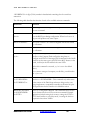
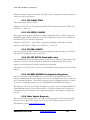
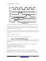
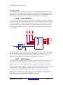
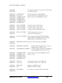
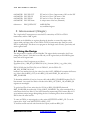
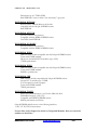
GCLK0 SELECT: 5326
GCLK1 SELECT: 5326
GCLK2 SELECT: DIV
The GCLK<n> SELECT instructions cause the global clock
networks to output a clock from an alternate source. When source
of GCLK0 is set to “5326”, then the global clock G0 is clocked
from the Si5326 synthesizer. When source of GCLK0 is set to
“STEP”, GCLK0 becomes a step clock, which can be accessed
through MCU configuration register 0xDF8F (see Chapter 4
Section 4.2.5 for details). “DIV” sets source to the Configuration
FPGA Divide clock and “SMA” selects the external SMA source.
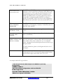
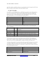
5326 <CLOCKNAME>
CLOCK FREQUENCY:
<number>MHz
The MCU will adjust the clock synthesizer producing clock
<clockname> to the frequency <number>. Valid clock names are
PH0, PH1, PH2, and REF
PH<phase number>
Divide By: 2^<N>
The divider for the PH<phase number> global clock will be set to
2^<N>.
MCU Register Write
0x<short addr>
0x<byte>
Writes to configuration register <short addr> with the value
<byte> (hexadecimal).
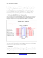
DCGCLK<dc clock
number> Select: <dc
source> [<n>MHz]
Sets the DCGCLK Clock Network DCLK<dc clock number> to
feed off of <dc source> (values are DC2, DC3, DC5, DC6, DC7,
DC8, or DC9). Then, enter a number for <n> to set the PLL
options. Omitting the last bracketed part will cause the PLLs to go
into bypass mode.
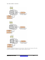
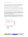
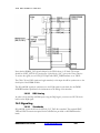
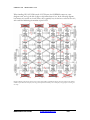
For valid combinations, please see the diagram in Section 4.4 of
this chapter.
Source: <clock> <n>
Sets <clock> to run from source <n>, where n=1 corresponds to
normal operation and n=2 corresponds to bypass mode, running
from F15 clock output. Clock can be “G0”,”G1”,”G2”.
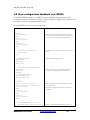
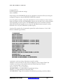
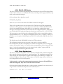
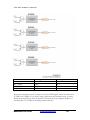
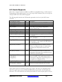
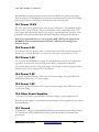
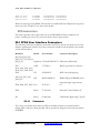
Figure 17 Main.txt Commands
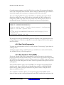
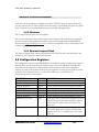
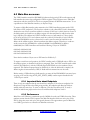
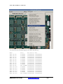
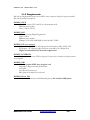
An example main.txt file is given below.
// This will prevent the MCU output over RS232 to speed up
configuration
VERBOSE LEVEL:2
//this will load the configuration a.bit into FPGA F0
FPGA 0: fpga_f0.bit
5326 PH0 CLOCK FREQUENCY: 300MHz
//Writes to a register in FPGA F0.
DN9000K10 User Guide
www.dinigroup.com
57