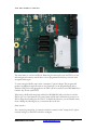
1
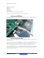
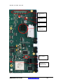
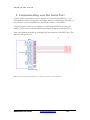
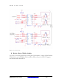
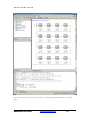
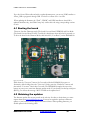
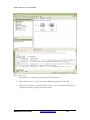
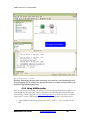
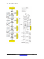
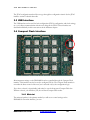
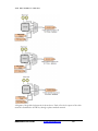
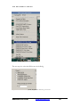
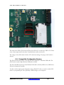
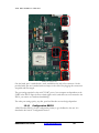
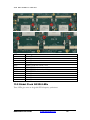
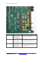
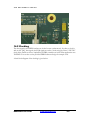
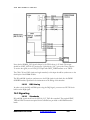
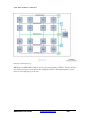
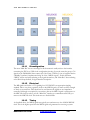
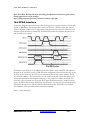
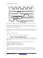
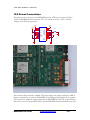
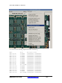
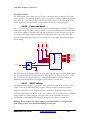
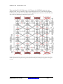
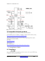
T H E
R E F E R E N C E
D E S I G N
Note that this is the same source as the “Main Reference Design”. To compile the design for
LVDS, some `define statements in the Verilog code must be added or removed. The make.bat
utility described in the “compiling the reference design” section automatically adds and removes
these directives. The pre-compiled bitfiles for this design are located at
D:\FPGA_Reference_Designs\Programming_Files\DN9000K10\LVDSIntercon\
13.2 Using the Design
The design‟s MainBus interface is undocumented
The IOs in the LVDS reference design are clocked using the G0 clock. A clock setting of
300MHz on G0 results in data transmission from FPGA to FPGA of 600Mbs per signal pair.
13.3 Running the Test
In the USB Controller program, select Settings->OneShot Test. From the dialog box, check the
Interconnect Test box. The program will automatically load the bit files, set the clocks and run
the test.
DN9000K10 User Guide
www.dinigroup.com
149