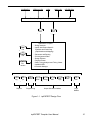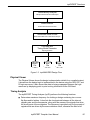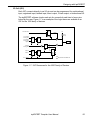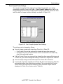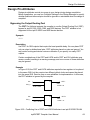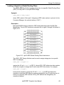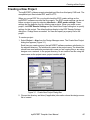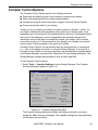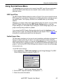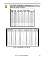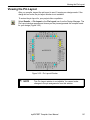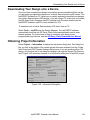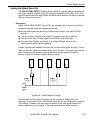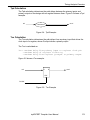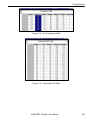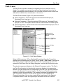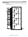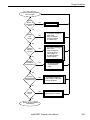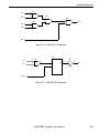
1
ispEXPERT Compiler
User Manual
Version 8.0
Technical Support Line: 1-800-LATTICE or (408) 428-6414
EXPERT-UM Rev 8.0.1
Copyright
This document may not, in whole or part, be copied, photocopied, reproduced,
translated, or reduced to any electronic medium or machine-readable form without
prior written consent from Lattice Semiconductor Corporation.
The software described in this manual is copyrighted and all rights are reserved by
Lattice Semiconductor Corporation. Information in this document is subject to change
without notice.
The distribution and sale of this product is intended for the use of the original
purchaser only and for use only on the computer system specified. Lawful users of
this product are hereby licensed only to read the programs on the disks, cassettes, or
tapes from their medium into the memory of a computer solely for the purpose of
executing them. Unauthorized copying, duplicating, selling, or otherwise distributing
this product is a violation of the law.
Trademarks
The following trademarks are recognized by Lattice Semiconductor Corporation:
Generic Array Logic, ISP, ispANALYZER, ispATE, ispCODE, ispDCD,
ispDOWNLOAD, ispDS, ispDS+, ispEXPERT, ispGDS, ispGDX, ispHDL, ispJTAG,
ispSmartFlow, ispStarter, ispSTREAM, ispSVF, ispTA, ispTEST, ispTURBO,
ispVECTOR, ispVerilog, ispVHDL, ispVM, Latch-Lock, LHDL, pDS+, RFT, Total ISP,
and Twin GLB are trademarks of Lattice Semiconductor Corporation.
E2CMOS, GAL, ispGAL, ispLSI, Lattice Semiconductor, Lattice Semiconductor Corp.,
Lattice designs, pDS, pLSI, Silicon Forest, and UltraMOS are registered trademarks
of Lattice Semiconductor Corporation.
Microsoft Windows is a registered trademark of Microsoft Corporation; MS-DOS is a
trademark of Microsoft Corporation.
IBM is a registered trademark of International Business Machines Corporation.
UNIX is a trademark of UNIX Systems Labs, Inc.
Sun-4, Sun Workstation, SPARCstation, and OpenWindows are registered
trademarks of Sun Microsystems.
Hewlett Packard (HP) is a registered trademark of Hewlett Packard, Inc. APOLLO,
HP-UX, HP-VUE, Series 400, and Series 700 are trademarks of Hewlett Packard,
Inc.
Lattice Semiconductor Corporation
5555 NE Moore Court
Hillsboro, OR 97124
(503) 268-8000
January 2000
ispEXPERT Compiler User Manual
2
Limited Warranty
Lattice Semiconductor Corporation warrants the original purchaser that the Lattice
Semiconductor software shall be free from defects in material and workmanship for a
period of ninety days from the date of purchase. If a defect covered by this limited
warranty occurs during this 90-day warranty period, Lattice Semiconductor will repair
or replace the component part at its option free of charge.
This limited warranty does not apply if the defects have been caused by negligence,
accident, unreasonable or unintended use, modification, or any causes not related to
defective materials or workmanship.
To receive service during the 90-day warranty period, contact Lattice Semiconductor
Corporation at:
Phone: 1-800-LATTICE
Fax: (408) 944-8450
E-mail: [email protected]
If the Lattice Semiconductor support personnel are unable to solve your problem over
the phone, we will provide you with instructions on returning your defective software
to us. The cost of returning the software to the Lattice Semiconductor Service Center
shall be paid by the purchaser.
Limitations on Warranty
Any applicable implied warranties, including warranties of merchantability and fitness
for a particular purpose, are hereby limited to ninety days from the date of purchase
and are subject to the conditions set forth herein. In no event shall Lattice
Semiconductor be liable for consequential or incidental damages resulting from the
breach of any expressed or implied warranties.
Purchaser’s sole remedy for any cause whatsoever, regardless of the form of action,
shall be limited to the price paid to Lattice Semiconductor for the ispEXPERT
software.
The provisions of this limited warranty are valid in the United States only. Some states
do not allow limitations on how long an implied warranty lasts, or exclusion of
consequential or incidental damages, so the above limitation or exclusion may not
apply to you.
This warranty provides you with specific legal rights. You may have other rights which
vary from state to state.
Acknowledgments
The ispEXPERT Compiler software is based on a Sequential Interactive System
(SIS) developed by the Computer-Aided Design (CAD) Research Group at the
University of California, Berkeley with significant enhancements and additions by
Lattice Semiconductor Corporation.
ispEXPERT Compiler User Manual
3
Table of Contents
Preface . . . . . . . . . . . . . . . . . . . . . . . . . . . . . . . . . . . . . . . . . . . . . . . . . . . . . . . . . . . . . . . . . . . 11
What Is In this User Manual. . . . . . . . . . . . . . . . . . . . . . . . . . . . . . . . . . . . . . . . . . . . . . . . . . .
Where to Look for Information . . . . . . . . . . . . . . . . . . . . . . . . . . . . . . . . . . . . . . . . . . . . . .
Related Documentation . . . . . . . . . . . . . . . . . . . . . . . . . . . . . . . . . . . . . . . . . . . . . . . . . . . . . .
Third-Party Interface Manuals . . . . . . . . . . . . . . . . . . . . . . . . . . . . . . . . . . . . . . . . . . . . . .
Documentation Conventions . . . . . . . . . . . . . . . . . . . . . . . . . . . . . . . . . . . . . . . . . . . . . . . . . .
12
12
13
13
14
Chapter 1 Introduction . . . . . . . . . . . . . . . . . . . . . . . . . . . . . . . . . . . . . . . . . . . . . . . . . . . 15
Third-Party Design Entry . . . . . . . . . . . . . . . . . . . . . . . . . . . . . . . . . . . . . . . . . . . . . . . . . . . . .
Running ispEXPERT . . . . . . . . . . . . . . . . . . . . . . . . . . . . . . . . . . . . . . . . . . . . . . . . . . . . . . . .
ispEXPERT Functions . . . . . . . . . . . . . . . . . . . . . . . . . . . . . . . . . . . . . . . . . . . . . . . . . . . . . . .
Design Analysis . . . . . . . . . . . . . . . . . . . . . . . . . . . . . . . . . . . . . . . . . . . . . . . . . . . . . . . . .
Synthesis and Partitioning . . . . . . . . . . . . . . . . . . . . . . . . . . . . . . . . . . . . . . . . . . . . . . . . .
Placement and Routing . . . . . . . . . . . . . . . . . . . . . . . . . . . . . . . . . . . . . . . . . . . . . . . . . . .
ispANALYZER . . . . . . . . . . . . . . . . . . . . . . . . . . . . . . . . . . . . . . . . . . . . . . . . . . . . . . . . . .
Physical Viewer . . . . . . . . . . . . . . . . . . . . . . . . . . . . . . . . . . . . . . . . . . . . . . . . . . . . . . . . .
Timing Analysis . . . . . . . . . . . . . . . . . . . . . . . . . . . . . . . . . . . . . . . . . . . . . . . . . . . . . . . . .
Timing Viewer. . . . . . . . . . . . . . . . . . . . . . . . . . . . . . . . . . . . . . . . . . . . . . . . . . . . . . . . . . .
ispEXPERT Output . . . . . . . . . . . . . . . . . . . . . . . . . . . . . . . . . . . . . . . . . . . . . . . . . . . . . . . . .
Netlist Formats . . . . . . . . . . . . . . . . . . . . . . . . . . . . . . . . . . . . . . . . . . . . . . . . . . . . . . . . . .
Fuse Map Generation. . . . . . . . . . . . . . . . . . . . . . . . . . . . . . . . . . . . . . . . . . . . . . . . . . . . .
Reports . . . . . . . . . . . . . . . . . . . . . . . . . . . . . . . . . . . . . . . . . . . . . . . . . . . . . . . . . . . . . . . .
Project Files . . . . . . . . . . . . . . . . . . . . . . . . . . . . . . . . . . . . . . . . . . . . . . . . . . . . . . . . . . . .
Designing with ispEXPERT . . . . . . . . . . . . . . . . . . . . . . . . . . . . . . . . . . . . . . . . . . . . . . . . . . .
Lattice Semiconductor Device Architecture . . . . . . . . . . . . . . . . . . . . . . . . . . . . . . . . . . . .
Generic Logic Blocks (GLB) . . . . . . . . . . . . . . . . . . . . . . . . . . . . . . . . . . . . . . . . . . . . .
I/O Cell (IOC) . . . . . . . . . . . . . . . . . . . . . . . . . . . . . . . . . . . . . . . . . . . . . . . . . . . . . . . .
Design Attributes . . . . . . . . . . . . . . . . . . . . . . . . . . . . . . . . . . . . . . . . . . . . . . . . . . . . . . . .
Compiler Control Options . . . . . . . . . . . . . . . . . . . . . . . . . . . . . . . . . . . . . . . . . . . . . . . . . .
Design Rules . . . . . . . . . . . . . . . . . . . . . . . . . . . . . . . . . . . . . . . . . . . . . . . . . . . . . . . . . . .
17
17
18
18
18
19
19
20
20
21
22
22
23
23
24
26
26
28
29
30
30
30
Chapter 2 Design Attributes . . . . . . . . . . . . . . . . . . . . . . . . . . . . . . . . . . . . . . . . . . . . . . 31
Applying Design Attributes. . . . . . . . . . . . . . . . . . . . . . . . . . . . . . . . . . . . . . . . . . . . . . . . . . . .
Precedence of Design Attributes . . . . . . . . . . . . . . . . . . . . . . . . . . . . . . . . . . . . . . . . . . . .
Design Attribute Syntax . . . . . . . . . . . . . . . . . . . . . . . . . . . . . . . . . . . . . . . . . . . . . . . . . . .
Net Attributes . . . . . . . . . . . . . . . . . . . . . . . . . . . . . . . . . . . . . . . . . . . . . . . . . . . . . . . . . . . . . .
Placing Logic into a Single BFM. . . . . . . . . . . . . . . . . . . . . . . . . . . . . . . . . . . . . . . . . . . . .
Assigning Device Clocks . . . . . . . . . . . . . . . . . . . . . . . . . . . . . . . . . . . . . . . . . . . . . . . . . .
ispEXPERT Compiler User Manual
33
34
34
35
35
36
4
Grouping GLB Outputs . . . . . . . . . . . . . . . . . . . . . . . . . . . . . . . . . . . . . . . . . . . . . . . . . . . .
Preventing the Elimination of Nets . . . . . . . . . . . . . . . . . . . . . . . . . . . . . . . . . . . . . . . . . . .
Preserving XOR Gates . . . . . . . . . . . . . . . . . . . . . . . . . . . . . . . . . . . . . . . . . . . . . . . . . . . .
Path Attributes . . . . . . . . . . . . . . . . . . . . . . . . . . . . . . . . . . . . . . . . . . . . . . . . . . . . . . . . . . . .
Specifying Asynchronous Paths . . . . . . . . . . . . . . . . . . . . . . . . . . . . . . . . . . . . . . . . . . . . .
Specifying Critical Paths. . . . . . . . . . . . . . . . . . . . . . . . . . . . . . . . . . . . . . . . . . . . . . . . . . .
Local Speed/Power Control . . . . . . . . . . . . . . . . . . . . . . . . . . . . . . . . . . . . . . . . . . . . . . . .
Low Power Path Toggle Setting . . . . . . . . . . . . . . . . . . . . . . . . . . . . . . . . . . . . . . . . . .
Turbo Path Setting . . . . . . . . . . . . . . . . . . . . . . . . . . . . . . . . . . . . . . . . . . . . . . . . . . . .
Post-Compile Turbo Settings . . . . . . . . . . . . . . . . . . . . . . . . . . . . . . . . . . . . . . . . . . . .
Specifying a No-Minimize Path. . . . . . . . . . . . . . . . . . . . . . . . . . . . . . . . . . . . . . . . . . . . . .
Symbol Attributes. . . . . . . . . . . . . . . . . . . . . . . . . . . . . . . . . . . . . . . . . . . . . . . . . . . . . . . . . . .
Implementing an Exclusive-Or . . . . . . . . . . . . . . . . . . . . . . . . . . . . . . . . . . . . . . . . . . . . . .
Optimizing Hard Macros . . . . . . . . . . . . . . . . . . . . . . . . . . . . . . . . . . . . . . . . . . . . . . . . . . .
Preventing Optimization of Primitives. . . . . . . . . . . . . . . . . . . . . . . . . . . . . . . . . . . . . . . . .
Placing a Register . . . . . . . . . . . . . . . . . . . . . . . . . . . . . . . . . . . . . . . . . . . . . . . . . . . . . . .
Design Pin Attributes . . . . . . . . . . . . . . . . . . . . . . . . . . . . . . . . . . . . . . . . . . . . . . . . . . . . . . . .
Bypassing the Output Routing Pool . . . . . . . . . . . . . . . . . . . . . . . . . . . . . . . . . . . . . . . . . .
Locking Package Pins . . . . . . . . . . . . . . . . . . . . . . . . . . . . . . . . . . . . . . . . . . . . . . . . . . . .
Locking a Signal to a Big Fast Megablock . . . . . . . . . . . . . . . . . . . . . . . . . . . . . . . . . . . . .
Locking a Signal to a Global Routing Plane . . . . . . . . . . . . . . . . . . . . . . . . . . . . . . . . . . . .
Reserving Package Pins . . . . . . . . . . . . . . . . . . . . . . . . . . . . . . . . . . . . . . . . . . . . . . . . . .
Local Device Attributes . . . . . . . . . . . . . . . . . . . . . . . . . . . . . . . . . . . . . . . . . . . . . . . . . . . . . .
Using Device Open-drain . . . . . . . . . . . . . . . . . . . . . . . . . . . . . . . . . . . . . . . . . . . . . . . . . .
Using Output Buffer Delays . . . . . . . . . . . . . . . . . . . . . . . . . . . . . . . . . . . . . . . . . . . . . . . .
Using Pull-up or Datahold. . . . . . . . . . . . . . . . . . . . . . . . . . . . . . . . . . . . . . . . . . . . . . . . . .
Setting Slow Slew Rate . . . . . . . . . . . . . . . . . . . . . . . . . . . . . . . . . . . . . . . . . . . . . . . . . . .
Setting Device Voltage . . . . . . . . . . . . . . . . . . . . . . . . . . . . . . . . . . . . . . . . . . . . . . . . . . . .
Constraint Manager . . . . . . . . . . . . . . . . . . . . . . . . . . . . . . . . . . . . . . . . . . . . . . . . . . . . . . . . .
Setting Attributes . . . . . . . . . . . . . . . . . . . . . . . . . . . . . . . . . . . . . . . . . . . . . . . . . . . . . . . .
Using the Constraint Manager with the Design Manager . . . . . . . . . . . . . . . . . . . . . . . . . .
39
40
43
45
47
50
53
53
54
55
56
58
58
59
61
62
64
64
65
67
68
69
71
71
71
72
73
73
74
75
77
Chapter 3 The Design Manager . . . . . . . . . . . . . . . . . . . . . . . . . . . . . . . . . . . . . . . . . . . 78
Creating a New Project . . . . . . . . . . . . . . . . . . . . . . . . . . . . . . . . . . . . . . . . . . . . . . . . . . . . . . 80
Opening a Project . . . . . . . . . . . . . . . . . . . . . . . . . . . . . . . . . . . . . . . . . . . . . . . . . . . . . . . . . . 83
Compiler Control Options. . . . . . . . . . . . . . . . . . . . . . . . . . . . . . . . . . . . . . . . . . . . . . . . . . . . . 84
Using the Interfaces Menu . . . . . . . . . . . . . . . . . . . . . . . . . . . . . . . . . . . . . . . . . . . . . . . . . . . . 88
EDIF Input Files . . . . . . . . . . . . . . . . . . . . . . . . . . . . . . . . . . . . . . . . . . . . . . . . . . . . . . . . . 88
Netlist Output Files . . . . . . . . . . . . . . . . . . . . . . . . . . . . . . . . . . . . . . . . . . . . . . . . . . . . . . . 88
Specifying a Device . . . . . . . . . . . . . . . . . . . . . . . . . . . . . . . . . . . . . . . . . . . . . . . . . . . . . . . . . 90
Specifying Pin Attributes . . . . . . . . . . . . . . . . . . . . . . . . . . . . . . . . . . . . . . . . . . . . . . . . . . . . . 92
Locking the Pins. . . . . . . . . . . . . . . . . . . . . . . . . . . . . . . . . . . . . . . . . . . . . . . . . . . . . . . . . . . . 95
Design Exploration. . . . . . . . . . . . . . . . . . . . . . . . . . . . . . . . . . . . . . . . . . . . . . . . . . . . . . . . . . 98
Naming and Saving Design Settings . . . . . . . . . . . . . . . . . . . . . . . . . . . . . . . . . . . . . . . . . . . 104
Setting the User Electronic Signature . . . . . . . . . . . . . . . . . . . . . . . . . . . . . . . . . . . . . . . . . . 106
Compiling Your Design . . . . . . . . . . . . . . . . . . . . . . . . . . . . . . . . . . . . . . . . . . . . . . . . . . . . . 107
Viewing the Pin Layout . . . . . . . . . . . . . . . . . . . . . . . . . . . . . . . . . . . . . . . . . . . . . . . . . . . . . 110
Changing the Pin Assignment . . . . . . . . . . . . . . . . . . . . . . . . . . . . . . . . . . . . . . . . . . . . . . . . 111
ispEXPERT Compiler User Manual
5
Viewing the Output Netlist Results. . . . . . . . . . . . . . . . . . . . . . . . . . . . . . . . . . . . . . . . . . . . .
Post-Compile Changes . . . . . . . . . . . . . . . . . . . . . . . . . . . . . . . . . . . . . . . . . . . . . . . . . . . . .
Importing a Pin File. . . . . . . . . . . . . . . . . . . . . . . . . . . . . . . . . . . . . . . . . . . . . . . . . . . . . .
Changing Pin Attributes . . . . . . . . . . . . . . . . . . . . . . . . . . . . . . . . . . . . . . . . . . . . . . . . . .
Analyzing Your Design. . . . . . . . . . . . . . . . . . . . . . . . . . . . . . . . . . . . . . . . . . . . . . . . . . . . . .
ispANALYZER Menus . . . . . . . . . . . . . . . . . . . . . . . . . . . . . . . . . . . . . . . . . . . . . . . . . . .
File Menu . . . . . . . . . . . . . . . . . . . . . . . . . . . . . . . . . . . . . . . . . . . . . . . . . . . . . . . . . .
Tools Menu . . . . . . . . . . . . . . . . . . . . . . . . . . . . . . . . . . . . . . . . . . . . . . . . . . . . . . . . .
Results Menu . . . . . . . . . . . . . . . . . . . . . . . . . . . . . . . . . . . . . . . . . . . . . . . . . . . . . . .
Using the Physical Viewer . . . . . . . . . . . . . . . . . . . . . . . . . . . . . . . . . . . . . . . . . . . . . . . . . . .
Downloading Your Design onto a Device . . . . . . . . . . . . . . . . . . . . . . . . . . . . . . . . . . . . . . .
Obtaining Project Information . . . . . . . . . . . . . . . . . . . . . . . . . . . . . . . . . . . . . . . . . . . . . . . .
Cleaning A Project Directory . . . . . . . . . . . . . . . . . . . . . . . . . . . . . . . . . . . . . . . . . . . . . . . . .
Updating a Project . . . . . . . . . . . . . . . . . . . . . . . . . . . . . . . . . . . . . . . . . . . . . . . . . . . . . . . . .
Using a Text File . . . . . . . . . . . . . . . . . . . . . . . . . . . . . . . . . . . . . . . . . . . . . . . . . . . . . . . . . .
Creating a Text File . . . . . . . . . . . . . . . . . . . . . . . . . . . . . . . . . . . . . . . . . . . . . . . . . . . . .
Saving a Text File. . . . . . . . . . . . . . . . . . . . . . . . . . . . . . . . . . . . . . . . . . . . . . . . . . . . . . .
Opening a Text File . . . . . . . . . . . . . . . . . . . . . . . . . . . . . . . . . . . . . . . . . . . . . . . . . . . . .
Editing a Text File. . . . . . . . . . . . . . . . . . . . . . . . . . . . . . . . . . . . . . . . . . . . . . . . . . . . . . .
Using Search and Replace. . . . . . . . . . . . . . . . . . . . . . . . . . . . . . . . . . . . . . . . . . . . . . . .
Clearing the Session Log . . . . . . . . . . . . . . . . . . . . . . . . . . . . . . . . . . . . . . . . . . . . . . . . .
Printing . . . . . . . . . . . . . . . . . . . . . . . . . . . . . . . . . . . . . . . . . . . . . . . . . . . . . . . . . . . . . . .
Optimizing Your Desktop . . . . . . . . . . . . . . . . . . . . . . . . . . . . . . . . . . . . . . . . . . . . . . . . . . . .
Changing the Screen Displays . . . . . . . . . . . . . . . . . . . . . . . . . . . . . . . . . . . . . . . . . . . . .
Changing the Pin Color and Shape and Message Color . . . . . . . . . . . . . . . . . . . . . . . . .
Closing a Project . . . . . . . . . . . . . . . . . . . . . . . . . . . . . . . . . . . . . . . . . . . . . . . . . . . . . . . . . .
111
112
112
113
115
116
116
116
117
117
118
118
119
120
121
121
121
121
122
122
123
123
124
124
125
127
Chapter 4 Design Compilation Options . . . . . . . . . . . . . . . . . . . . . . . . . . . . . . . . . . 128
Compiler Control Options. . . . . . . . . . . . . . . . . . . . . . . . . . . . . . . . . . . . . . . . . . . . . . . . . . . .
BFM Packing for Improved Routability . . . . . . . . . . . . . . . . . . . . . . . . . . . . . . . . . . . . . . .
Maintaining Pin Direction . . . . . . . . . . . . . . . . . . . . . . . . . . . . . . . . . . . . . . . . . . . . . . . . .
Specifying Case Sensitivity . . . . . . . . . . . . . . . . . . . . . . . . . . . . . . . . . . . . . . . . . . . . . . .
Controlling Optimization . . . . . . . . . . . . . . . . . . . . . . . . . . . . . . . . . . . . . . . . . . . . . . . . . .
Setting Effort Levels . . . . . . . . . . . . . . . . . . . . . . . . . . . . . . . . . . . . . . . . . . . . . . . . . .
Choosing Optimization Strategies. . . . . . . . . . . . . . . . . . . . . . . . . . . . . . . . . . . . . . . .
Controlling Routing Time . . . . . . . . . . . . . . . . . . . . . . . . . . . . . . . . . . . . . . . . . . . . . . . . .
Controlling Pin Assignments. . . . . . . . . . . . . . . . . . . . . . . . . . . . . . . . . . . . . . . . . . . . . . .
Ignoring Fixed Pins . . . . . . . . . . . . . . . . . . . . . . . . . . . . . . . . . . . . . . . . . . . . . . . . . . .
Using a Pin File . . . . . . . . . . . . . . . . . . . . . . . . . . . . . . . . . . . . . . . . . . . . . . . . . . . . . .
Identifying Input Files . . . . . . . . . . . . . . . . . . . . . . . . . . . . . . . . . . . . . . . . . . . . . . . . . . . .
Specifying the Name of an Input File . . . . . . . . . . . . . . . . . . . . . . . . . . . . . . . . . . . . .
Specifying the Format of an Input File . . . . . . . . . . . . . . . . . . . . . . . . . . . . . . . . . . . .
Controlling GLB Inputs and Outputs. . . . . . . . . . . . . . . . . . . . . . . . . . . . . . . . . . . . . . . . .
Specifying Maximum GLB Inputs . . . . . . . . . . . . . . . . . . . . . . . . . . . . . . . . . . . . . . . .
Specifying Maximum GLB Outputs . . . . . . . . . . . . . . . . . . . . . . . . . . . . . . . . . . . . . . .
Minimizing GLB Levels . . . . . . . . . . . . . . . . . . . . . . . . . . . . . . . . . . . . . . . . . . . . . . . . . . .
Creating Netlists . . . . . . . . . . . . . . . . . . . . . . . . . . . . . . . . . . . . . . . . . . . . . . . . . . . . . . . .
Specifying the Format of an Output File . . . . . . . . . . . . . . . . . . . . . . . . . . . . . . . . . . .
ispEXPERT Compiler User Manual
129
130
131
131
132
132
132
134
135
135
136
137
137
137
138
138
139
141
142
142
6
Specifying a Viewlogic Timing File Name . . . . . . . . . . . . . . . . . . . . . . . . . . . . . . . . . .
Specifying a Parameter File . . . . . . . . . . . . . . . . . . . . . . . . . . . . . . . . . . . . . . . . . . . . . . .
Specifying a Part Number. . . . . . . . . . . . . . . . . . . . . . . . . . . . . . . . . . . . . . . . . . . . . . . . .
Specifying a Property File. . . . . . . . . . . . . . . . . . . . . . . . . . . . . . . . . . . . . . . . . . . . . . . . .
Single PT Packing for Improved Routability . . . . . . . . . . . . . . . . . . . . . . . . . . . . . . . . . . .
Performing Batch Mode Timing Analysis . . . . . . . . . . . . . . . . . . . . . . . . . . . . . . . . . . . . .
Using the Internal Tristate IO Driver . . . . . . . . . . . . . . . . . . . . . . . . . . . . . . . . . . . . . . . . .
Global Device Options . . . . . . . . . . . . . . . . . . . . . . . . . . . . . . . . . . . . . . . . . . . . . . . . . . . . . .
Using In-System Programming Pins. . . . . . . . . . . . . . . . . . . . . . . . . . . . . . . . . . . . . . . . .
Using the Y2 Pin as a Clock Input . . . . . . . . . . . . . . . . . . . . . . . . . . . . . . . . . . . . . . . . . .
Using the TOE/IO Shared Pin . . . . . . . . . . . . . . . . . . . . . . . . . . . . . . . . . . . . . . . . . . . . .
Setting the Global Reset Pin . . . . . . . . . . . . . . . . . . . . . . . . . . . . . . . . . . . . . . . . . . . . . .
Setting the Y1/RESET Pin . . . . . . . . . . . . . . . . . . . . . . . . . . . . . . . . . . . . . . . . . . . . . . . .
Preserving XOR Gates . . . . . . . . . . . . . . . . . . . . . . . . . . . . . . . . . . . . . . . . . . . . . . . . . . .
Global Speed/Power Control . . . . . . . . . . . . . . . . . . . . . . . . . . . . . . . . . . . . . . . . . . . . . .
Global Speed/Power Control. . . . . . . . . . . . . . . . . . . . . . . . . . . . . . . . . . . . . . . . . . . .
Using Device Open-drain . . . . . . . . . . . . . . . . . . . . . . . . . . . . . . . . . . . . . . . . . . . . . . . . .
Using Output Buffer Delays . . . . . . . . . . . . . . . . . . . . . . . . . . . . . . . . . . . . . . . . . . . . . . .
Using Pull-up or Datahold. . . . . . . . . . . . . . . . . . . . . . . . . . . . . . . . . . . . . . . . . . . . . . . . .
Setting Slow Slew Rate . . . . . . . . . . . . . . . . . . . . . . . . . . . . . . . . . . . . . . . . . . . . . . . . . .
Setting Device Voltage . . . . . . . . . . . . . . . . . . . . . . . . . . . . . . . . . . . . . . . . . . . . . . . . . . .
Setting Device Security . . . . . . . . . . . . . . . . . . . . . . . . . . . . . . . . . . . . . . . . . . . . . . . . . .
Using a Parameter File . . . . . . . . . . . . . . . . . . . . . . . . . . . . . . . . . . . . . . . . . . . . . . . . . . . . .
Parameter File Rules . . . . . . . . . . . . . . . . . . . . . . . . . . . . . . . . . . . . . . . . . . . . . . . . . . . .
Parameter File Example . . . . . . . . . . . . . . . . . . . . . . . . . . . . . . . . . . . . . . . . . . . . . . . . . .
Invoking the Compiler from the Command Line. . . . . . . . . . . . . . . . . . . . . . . . . . . . . . . . . . .
Command Syntax . . . . . . . . . . . . . . . . . . . . . . . . . . . . . . . . . . . . . . . . . . . . . . . . . . . .
Definitions . . . . . . . . . . . . . . . . . . . . . . . . . . . . . . . . . . . . . . . . . . . . . . . . . . . . . . . . . .
Examples . . . . . . . . . . . . . . . . . . . . . . . . . . . . . . . . . . . . . . . . . . . . . . . . . . . . . . . . . . . . .
Script Files . . . . . . . . . . . . . . . . . . . . . . . . . . . . . . . . . . . . . . . . . . . . . . . . . . . . . . . . . . . .
143
144
145
145
146
147
148
149
150
151
152
153
154
156
157
157
158
159
159
161
161
162
163
163
164
165
165
165
166
167
Chapter 5 Timing Analysis . . . . . . . . . . . . . . . . . . . . . . . . . . . . . . . . . . . . . . . . . . . . . . 168
Timing Analysis Overview . . . . . . . . . . . . . . . . . . . . . . . . . . . . . . . . . . . . . . . . . . . . . . . . . . .
Path Analysis . . . . . . . . . . . . . . . . . . . . . . . . . . . . . . . . . . . . . . . . . . . . . . . . . . . . . . . . . .
Frequency Calculation . . . . . . . . . . . . . . . . . . . . . . . . . . . . . . . . . . . . . . . . . . . . . . . . . . .
Frequency Calculation Example . . . . . . . . . . . . . . . . . . . . . . . . . . . . . . . . . . . . . . . . .
Setup and Hold Time Evaluation . . . . . . . . . . . . . . . . . . . . . . . . . . . . . . . . . . . . . . . . . . .
Setup Time . . . . . . . . . . . . . . . . . . . . . . . . . . . . . . . . . . . . . . . . . . . . . . . . . . . . . . . . .
Hold Time . . . . . . . . . . . . . . . . . . . . . . . . . . . . . . . . . . . . . . . . . . . . . . . . . . . . . . . . . .
Setup and Hold Time Example . . . . . . . . . . . . . . . . . . . . . . . . . . . . . . . . . . . . . . . . . .
Tpd Calculation. . . . . . . . . . . . . . . . . . . . . . . . . . . . . . . . . . . . . . . . . . . . . . . . . . . . . . . . .
Tco Calculation. . . . . . . . . . . . . . . . . . . . . . . . . . . . . . . . . . . . . . . . . . . . . . . . . . . . . . . . .
Path Enumeration. . . . . . . . . . . . . . . . . . . . . . . . . . . . . . . . . . . . . . . . . . . . . . . . . . . . . . .
Longest and Shortest Path Example. . . . . . . . . . . . . . . . . . . . . . . . . . . . . . . . . . . . . .
GLB Boundary Calculation . . . . . . . . . . . . . . . . . . . . . . . . . . . . . . . . . . . . . . . . . . . . . . . .
ispEXPERT Timing Analyzer . . . . . . . . . . . . . . . . . . . . . . . . . . . . . . . . . . . . . . . . . . . . . . . . .
Running the Timing Analyzer . . . . . . . . . . . . . . . . . . . . . . . . . . . . . . . . . . . . . . . . . . . . . .
Timing Analyzer Report Files . . . . . . . . . . . . . . . . . . . . . . . . . . . . . . . . . . . . . . . . . . . . . .
ispEXPERT Compiler User Manual
169
169
170
170
172
172
172
173
174
174
175
176
177
178
178
181
7
Timing Explorer . . . . . . . . . . . . . . . . . . . . . . . . . . . . . . . . . . . . . . . . . . . . . . . . . . . . . . . . . . .
Signal Navigator . . . . . . . . . . . . . . . . . . . . . . . . . . . . . . . . . . . . . . . . . . . . . . . . . . . . . . . .
Pop-up Menus from the Signal Navigator. . . . . . . . . . . . . . . . . . . . . . . . . . . . . . . . . . . . .
Timing Explorer Tables. . . . . . . . . . . . . . . . . . . . . . . . . . . . . . . . . . . . . . . . . . . . . . . . . . .
Pop-Up Menus from the Timing Tables . . . . . . . . . . . . . . . . . . . . . . . . . . . . . . . . . . . . . .
Timing Path Report. . . . . . . . . . . . . . . . . . . . . . . . . . . . . . . . . . . . . . . . . . . . . . . . . . . . . .
Running the Timing Analyzer from the Command Line . . . . . . . . . . . . . . . . . . . . . . . . . . . . .
Power Calculation . . . . . . . . . . . . . . . . . . . . . . . . . . . . . . . . . . . . . . . . . . . . . . . . . . . . . . . . .
183
183
184
185
187
188
189
190
Chapter 6 The Physical Viewer . . . . . . . . . . . . . . . . . . . . . . . . . . . . . . . . . . . . . . . . . . 192
Running the Physical Viewer . . . . . . . . . . . . . . . . . . . . . . . . . . . . . . . . . . . . . . . . . . . . . . . . .
Design Navigator Window . . . . . . . . . . . . . . . . . . . . . . . . . . . . . . . . . . . . . . . . . . . . . . . . . . .
Connectivity Window . . . . . . . . . . . . . . . . . . . . . . . . . . . . . . . . . . . . . . . . . . . . . . . . . . . . . . .
Connectivity Views . . . . . . . . . . . . . . . . . . . . . . . . . . . . . . . . . . . . . . . . . . . . . . . . . . . . . .
Customizing the Connectivity Window . . . . . . . . . . . . . . . . . . . . . . . . . . . . . . . . . . . . . . .
Display Modes . . . . . . . . . . . . . . . . . . . . . . . . . . . . . . . . . . . . . . . . . . . . . . . . . . . . . . . . .
Path Tracer . . . . . . . . . . . . . . . . . . . . . . . . . . . . . . . . . . . . . . . . . . . . . . . . . . . . . . . . . . . . . .
Obtaining Additional Information . . . . . . . . . . . . . . . . . . . . . . . . . . . . . . . . . . . . . . . . . . . . . .
GLB Information . . . . . . . . . . . . . . . . . . . . . . . . . . . . . . . . . . . . . . . . . . . . . . . . . . . . . . . .
Module Information. . . . . . . . . . . . . . . . . . . . . . . . . . . . . . . . . . . . . . . . . . . . . . . . . . . . . .
IOC Information . . . . . . . . . . . . . . . . . . . . . . . . . . . . . . . . . . . . . . . . . . . . . . . . . . . . . . . .
Dedicated/Control Input Information. . . . . . . . . . . . . . . . . . . . . . . . . . . . . . . . . . . . . . . . .
GLB Pin Information . . . . . . . . . . . . . . . . . . . . . . . . . . . . . . . . . . . . . . . . . . . . . . . . . . . . .
Statistics . . . . . . . . . . . . . . . . . . . . . . . . . . . . . . . . . . . . . . . . . . . . . . . . . . . . . . . . . . . . . .
Observability Information for GLB Pins . . . . . . . . . . . . . . . . . . . . . . . . . . . . . . . . . . . . . .
Timing Information . . . . . . . . . . . . . . . . . . . . . . . . . . . . . . . . . . . . . . . . . . . . . . . . . . . . . .
193
194
196
198
199
201
206
207
207
209
210
210
211
212
213
213
Chapter 7 Design Reports . . . . . . . . . . . . . . . . . . . . . . . . . . . . . . . . . . . . . . . . . . . . . . . 214
Example Design. . . . . . . . . . . . . . . . . . . . . . . . . . . . . . . . . . . . . . . . . . . . . . . . . . . . . . . . . . .
Compilation Report . . . . . . . . . . . . . . . . . . . . . . . . . . . . . . . . . . . . . . . . . . . . . . . . . . . . . . . .
Design Parameters Section . . . . . . . . . . . . . . . . . . . . . . . . . . . . . . . . . . . . . . . . . . . . . . .
Design Specification Section . . . . . . . . . . . . . . . . . . . . . . . . . . . . . . . . . . . . . . . . . . . . . .
Pre-Route Design Statistics Section. . . . . . . . . . . . . . . . . . . . . . . . . . . . . . . . . . . . . . . . .
Post-Route Design Implementation Section. . . . . . . . . . . . . . . . . . . . . . . . . . . . . . . . . . .
GLB Equations . . . . . . . . . . . . . . . . . . . . . . . . . . . . . . . . . . . . . . . . . . . . . . . . . . . . . .
GLB Equations Example . . . . . . . . . . . . . . . . . . . . . . . . . . . . . . . . . . . . . . . . . . . . . . .
Module Section . . . . . . . . . . . . . . . . . . . . . . . . . . . . . . . . . . . . . . . . . . . . . . . . . . . . . .
Pin and Clock Information . . . . . . . . . . . . . . . . . . . . . . . . . . . . . . . . . . . . . . . . . . . . .
Summary Statistics . . . . . . . . . . . . . . . . . . . . . . . . . . . . . . . . . . . . . . . . . . . . . . . . . . .
Pre-Route Design Implementation Section . . . . . . . . . . . . . . . . . . . . . . . . . . . . . . . . . . .
Fail to Fit Information . . . . . . . . . . . . . . . . . . . . . . . . . . . . . . . . . . . . . . . . . . . . . . . . .
Compilation Report for the ispLSI 5000V/8000 Devices . . . . . . . . . . . . . . . . . . . . . . . . . . . .
Design Specification Section . . . . . . . . . . . . . . . . . . . . . . . . . . . . . . . . . . . . . . . . . . . . . .
Post-Route Design Implementation Section. . . . . . . . . . . . . . . . . . . . . . . . . . . . . . . . . . .
Timing Analyzer Reports . . . . . . . . . . . . . . . . . . . . . . . . . . . . . . . . . . . . . . . . . . . . . . . . . . . .
Frequency Analysis Report . . . . . . . . . . . . . . . . . . . . . . . . . . . . . . . . . . . . . . . . . . . . . . .
Setup and Hold Report . . . . . . . . . . . . . . . . . . . . . . . . . . . . . . . . . . . . . . . . . . . . . . . . . .
Tco Report . . . . . . . . . . . . . . . . . . . . . . . . . . . . . . . . . . . . . . . . . . . . . . . . . . . . . . . . . . . .
ispEXPERT Compiler User Manual
215
216
217
218
220
222
222
224
227
228
231
234
236
237
237
238
248
248
250
251
8
Tpd Report . . . . . . . . . . . . . . . . . . . . . . . . . . . . . . . . . . . . . . . . . . . . . . . . . . . . . . . . . . . .
Selected Path Summary Report Example . . . . . . . . . . . . . . . . . . . . . . . . . . . . . . . . . . . .
Selected Path Detailed Report Example . . . . . . . . . . . . . . . . . . . . . . . . . . . . . . . . . . . . .
Selected Path Boundary Report Example . . . . . . . . . . . . . . . . . . . . . . . . . . . . . . . . . . . .
6192 Report . . . . . . . . . . . . . . . . . . . . . . . . . . . . . . . . . . . . . . . . . . . . . . . . . . . . . . . . . . .
252
253
255
258
261
Appendix A Design Rules and Tips . . . . . . . . . . . . . . . . . . . . . . . . . . . . . . . . . . . . . . 264
Design Problems . . . . . . . . . . . . . . . . . . . . . . . . . . . . . . . . . . . . . . . . . . . . . . . . . . . . . . . . . .
System, Syntax, and Specification Errors . . . . . . . . . . . . . . . . . . . . . . . . . . . . . . . . . . . . . . .
System Errors. . . . . . . . . . . . . . . . . . . . . . . . . . . . . . . . . . . . . . . . . . . . . . . . . . . . . . . . . .
Reserved File Names . . . . . . . . . . . . . . . . . . . . . . . . . . . . . . . . . . . . . . . . . . . . . . . . .
Syntax Errors . . . . . . . . . . . . . . . . . . . . . . . . . . . . . . . . . . . . . . . . . . . . . . . . . . . . . . . . . .
Valid Characters . . . . . . . . . . . . . . . . . . . . . . . . . . . . . . . . . . . . . . . . . . . . . . . . . . . . .
Valid Identifiers and Text. . . . . . . . . . . . . . . . . . . . . . . . . . . . . . . . . . . . . . . . . . . . . . .
Specification Errors and Problems . . . . . . . . . . . . . . . . . . . . . . . . . . . . . . . . . . . . . . . . . .
Attribute and Option Names and Values. . . . . . . . . . . . . . . . . . . . . . . . . . . . . . . . . . .
Keywords . . . . . . . . . . . . . . . . . . . . . . . . . . . . . . . . . . . . . . . . . . . . . . . . . . . . . . . . . .
Duplicate Names. . . . . . . . . . . . . . . . . . . . . . . . . . . . . . . . . . . . . . . . . . . . . . . . . . . . .
Optimizing Your Design . . . . . . . . . . . . . . . . . . . . . . . . . . . . . . . . . . . . . . . . . . . . . . . . . . . . .
Resizing your Design . . . . . . . . . . . . . . . . . . . . . . . . . . . . . . . . . . . . . . . . . . . . . . . . . . . .
Optimizing for Resource Utilization . . . . . . . . . . . . . . . . . . . . . . . . . . . . . . . . . . . . . . . . .
Improving Routability . . . . . . . . . . . . . . . . . . . . . . . . . . . . . . . . . . . . . . . . . . . . . . . . . . . . . . .
Optimizing for Routability . . . . . . . . . . . . . . . . . . . . . . . . . . . . . . . . . . . . . . . . . . . . . . . . .
Design Simulation . . . . . . . . . . . . . . . . . . . . . . . . . . . . . . . . . . . . . . . . . . . . . . . . . . . . . . . . .
Improving a Working Design . . . . . . . . . . . . . . . . . . . . . . . . . . . . . . . . . . . . . . . . . . . . . . . . .
Optimizing for Speed . . . . . . . . . . . . . . . . . . . . . . . . . . . . . . . . . . . . . . . . . . . . . . . . . . . .
Design Runtime and Memory Requirements . . . . . . . . . . . . . . . . . . . . . . . . . . . . . . . . . .
Design Rules . . . . . . . . . . . . . . . . . . . . . . . . . . . . . . . . . . . . . . . . . . . . . . . . . . . . . . . . . . . . .
I/O Pin Designations. . . . . . . . . . . . . . . . . . . . . . . . . . . . . . . . . . . . . . . . . . . . . . . . . . . . .
Output Enable Signals . . . . . . . . . . . . . . . . . . . . . . . . . . . . . . . . . . . . . . . . . . . . . . . . . . .
Global Reset Signal . . . . . . . . . . . . . . . . . . . . . . . . . . . . . . . . . . . . . . . . . . . . . . . . . . . . .
Generic Logic Blocks and Megablocks (ispLSI 1000, 2000, and 3000 Devices) . . . . . . .
Modules (ispLSI 6000 devices) . . . . . . . . . . . . . . . . . . . . . . . . . . . . . . . . . . . . . . . . . . . .
Nets . . . . . . . . . . . . . . . . . . . . . . . . . . . . . . . . . . . . . . . . . . . . . . . . . . . . . . . . . . . . . . . . .
Clock Usage . . . . . . . . . . . . . . . . . . . . . . . . . . . . . . . . . . . . . . . . . . . . . . . . . . . . . . . . . . .
Designing for ispLSI 5000V and 8000 Devices . . . . . . . . . . . . . . . . . . . . . . . . . . . . . . . . . . .
Considerations for ispLSI 5000V Devices . . . . . . . . . . . . . . . . . . . . . . . . . . . . . . . . . . . .
Considerations for ispLSI 8000 Devices. . . . . . . . . . . . . . . . . . . . . . . . . . . . . . . . . . . . . .
ispLSI 8000 Tristate Usage. . . . . . . . . . . . . . . . . . . . . . . . . . . . . . . . . . . . . . . . . . . . .
264
266
266
266
266
266
267
268
268
268
268
268
269
269
270
270
275
276
277
277
278
278
279
279
279
279
280
280
281
281
281
282
Appendix B - EDIF Property File . . . . . . . . . . . . . . . . . . . . . . . . . . . . . . . . . . . . . . . . . 283
Scope and Precedence Rules . . . . . . . . . . . . . . . . . . . . . . . . . . . . . . . . . . . . . . . . . . . . . . . .
EDIF Reader . . . . . . . . . . . . . . . . . . . . . . . . . . . . . . . . . . . . . . . . . . . . . . . . . . . . . . . . . . . . .
EDIF Property File Syntax . . . . . . . . . . . . . . . . . . . . . . . . . . . . . . . . . . . . . . . . . . . . . . . . . . .
Syntax Definitions. . . . . . . . . . . . . . . . . . . . . . . . . . . . . . . . . . . . . . . . . . . . . . . . . . . . . . .
Syntax Rules . . . . . . . . . . . . . . . . . . . . . . . . . . . . . . . . . . . . . . . . . . . . . . . . . . . . . . . . . .
Design Attributes . . . . . . . . . . . . . . . . . . . . . . . . . . . . . . . . . . . . . . . . . . . . . . . . . . . . . . . . . .
Pin Attributes . . . . . . . . . . . . . . . . . . . . . . . . . . . . . . . . . . . . . . . . . . . . . . . . . . . . . . . . . .
ispEXPERT Compiler User Manual
284
284
286
286
288
289
289
9
Pin Array Attributes. . . . . . . . . . . . . . . . . . . . . . . . . . . . . . . . . . . . . . . . . . . . . . . . . . . . . .
Net Attributes . . . . . . . . . . . . . . . . . . . . . . . . . . . . . . . . . . . . . . . . . . . . . . . . . . . . . . . . . .
Path Attributes . . . . . . . . . . . . . . . . . . . . . . . . . . . . . . . . . . . . . . . . . . . . . . . . . . . . . . . . .
Symbol Attributes . . . . . . . . . . . . . . . . . . . . . . . . . . . . . . . . . . . . . . . . . . . . . . . . . . . . . . .
Attribute Examples. . . . . . . . . . . . . . . . . . . . . . . . . . . . . . . . . . . . . . . . . . . . . . . . . . . . . . . . .
Pin Attributes . . . . . . . . . . . . . . . . . . . . . . . . . . . . . . . . . . . . . . . . . . . . . . . . . . . . . . . . . .
Pin Array Attributes. . . . . . . . . . . . . . . . . . . . . . . . . . . . . . . . . . . . . . . . . . . . . . . . . . . . . .
Net and Path Attributes . . . . . . . . . . . . . . . . . . . . . . . . . . . . . . . . . . . . . . . . . . . . . . . . . .
Symbol Attributes . . . . . . . . . . . . . . . . . . . . . . . . . . . . . . . . . . . . . . . . . . . . . . . . . . . . . . .
Parameterized Attributes . . . . . . . . . . . . . . . . . . . . . . . . . . . . . . . . . . . . . . . . . . . . . . . . .
Multiple Property Identifiers . . . . . . . . . . . . . . . . . . . . . . . . . . . . . . . . . . . . . . . . . . . . . . .
EDIF Reader Command Line Syntax. . . . . . . . . . . . . . . . . . . . . . . . . . . . . . . . . . . . . . . . . . .
290
291
292
293
294
294
296
297
299
303
306
307
Appendix C Menu and Icon Reference . . . . . . . . . . . . . . . . . . . . . . . . . . . . . . . . . . . 308
ispEXPERT Compiler. . . . . . . . . . . . . . . . . . . . . . . . . . . . . . . . . . . . . . . . . . . . . . . . . . . . . . .
Pull-Down Menus . . . . . . . . . . . . . . . . . . . . . . . . . . . . . . . . . . . . . . . . . . . . . . . . . . . . . . .
Tool Bar Icons . . . . . . . . . . . . . . . . . . . . . . . . . . . . . . . . . . . . . . . . . . . . . . . . . . . . . . . . .
ispANALYZER . . . . . . . . . . . . . . . . . . . . . . . . . . . . . . . . . . . . . . . . . . . . . . . . . . . . . . . . . . . .
Pull-Down Menus . . . . . . . . . . . . . . . . . . . . . . . . . . . . . . . . . . . . . . . . . . . . . . . . . . . . . . .
Tool Bar Icons . . . . . . . . . . . . . . . . . . . . . . . . . . . . . . . . . . . . . . . . . . . . . . . . . . . . . . . . .
Physical Viewer . . . . . . . . . . . . . . . . . . . . . . . . . . . . . . . . . . . . . . . . . . . . . . . . . . . . . . . . . . .
Pull-Down Menus . . . . . . . . . . . . . . . . . . . . . . . . . . . . . . . . . . . . . . . . . . . . . . . . . . . . . . .
Tool Bar Icons . . . . . . . . . . . . . . . . . . . . . . . . . . . . . . . . . . . . . . . . . . . . . . . . . . . . . . . . .
Timing Viewer . . . . . . . . . . . . . . . . . . . . . . . . . . . . . . . . . . . . . . . . . . . . . . . . . . . . . . . . . . . .
Pull-Down Menus . . . . . . . . . . . . . . . . . . . . . . . . . . . . . . . . . . . . . . . . . . . . . . . . . . . . . . .
Tool Bar Icons . . . . . . . . . . . . . . . . . . . . . . . . . . . . . . . . . . . . . . . . . . . . . . . . . . . . . . . . .
Constraint Manager . . . . . . . . . . . . . . . . . . . . . . . . . . . . . . . . . . . . . . . . . . . . . . . . . . . . . . . .
Pull-Down Menus . . . . . . . . . . . . . . . . . . . . . . . . . . . . . . . . . . . . . . . . . . . . . . . . . . . . . . .
Tool Bar Icons . . . . . . . . . . . . . . . . . . . . . . . . . . . . . . . . . . . . . . . . . . . . . . . . . . . . . . . . .
309
309
312
314
314
316
317
317
318
320
320
321
322
322
323
Glossary . . . . . . . . . . . . . . . . . . . . . . . . . . . . . . . . . . . . . . . . . . . . . . . . . . . . . . . . . . . . . . . . . 324
ispEXPERT Compiler User Manual
10
Preface
The ispEXPERT™ Compiler software (referred to as ispEXPERT) is used to optimize,
partition, place, and route logic designs for the Lattice Semiconductor in-system
programmable Large Scale Integrated (ispLSI®) devices.
This user manual describes the capabilities and use of the ispEXPERT software. It is
written for design engineers who understand system and logic design and the use of
design automation software. You should also understand how to perform basic
procedures using your operating system. This manual contains information to guide
you through compilation and device programming. It is the primary learning guide to
help you use the software to design with Lattice Semiconductor ispLSI devices. This
manual shows screens captured in Windows 95. If you are using a workstation or a
different Windows product, the appearance of the screens may differ slightly.
Some technical reference material is included in this user manual to provide you with
background material. However, you should be familiar with the Lattice Semiconductor
device architecture. Read the Lattice Semiconductor ISP Encyclopedia to fully
understand all the features of the Lattice Semiconductor devices.
ispEXPERT Compiler User Manual
11
What Is In this User Manual
What Is In this User Manual
This user manual contains information and procedures on the following topics:
■
■
■
■
■
■
■
■
■
■
■
■
■
■
Using Design Attributes to specify design constraints
Using the Design Manager to lock pins and set pin attributes
Using Compiler Control Options to specify design objectives
Using the Explore function to determine compilation trial results
Running the ispEXPERT compiler
Using the ispANALYZER™
Using the Static Timing Analyzer (ispTA™)
Using the Timing Viewer
Using the Physical Viewer
Understanding log and report files
Design rules and tips
Parameter File syntax
Property File syntax
Command line syntax
Where to Look for Information
Chapter 1, Introduction – Provides an overview of ispEXPERT and its design flow.
Chapter 2, Design Attributes – Describes how Design Attributes can be used to
specify design constraints.
Chapter 3, Design Compilation and Control – Provides information on using the
ispEXPERT Design Manager.
Chapter 4, Design Compilation Options – Describes each Compiler Control Option
and provides the Design Manager sequence, the parameter file syntax, and the
command line syntax. Also describes a Parameter File and the Design Process
Manager (dpm).
Chapter 5, Timing Analysis – Provides information on using the Timing Analyzer
(ispTA™) and the Timing Viewer.
Chapter 6, Physical Viewer – Describes the Physical Viewer and its relationship to
the Timing Viewer and the information it provides.
Chapter 7, Design Reports – Explains the different sections that make up the
post-route and pre-route compiler report files and provides examples of timing
reports.
ispEXPERT Compiler User Manual
12
Related Documentation
Appendix A, Design Rules and Tips – Describes device-dependent design rules
and user tips to optimize designs for delay, area, or routability.
Appendix B, EDIF Property File – Provides the EDIF Property File syntax.
Appendix C, Menu and Icon Reference – Shows the menus and tool bar icons for
the ispEXPERT Compiler Design Manager, the ispANALYZER, the Physical Viewer,
and the Timing Viewer.
Related Documentation
In addition to this user manual, the following documentation is useful when using the
Lattice Semiconductor ispEXPERT compiler software:
■
■
■
■
■
■
■
ispEXPERT Compiler Getting Started Manual
ispEXPERT Compiler Release Notes
ISP Encyclopedia
ISP Daisy Chain Download User Manual (PC only)
Macro Library Reference Manual
5K/8K Macro Library Supplement
VHDL and Verilog Simulation User Manual
These manuals, as well as the interface manuals listed below, are located in the
manuals directory on the CD-ROM. The ISP Encyclopedia is located in the databook
directory. These documents can be downloaded to a local drive or accessed on the
CD-ROM. The ispEXPERT Help menu also provides access to the manuals.
Third-Party Interface Manuals
Use the ispEXPERT Compiler software to compile designs from many third-party
CAE environments. The following is a list of manuals that Lattice Semiconductor
provides as support to the various third-party interfaces.
■
■
■
■
■
■
■
Altera to Lattice Semiconductor Design Conversion Application Notes
ispEXPERT Compiler and Cadence Design Manual
ispEXPERT Compiler and Exemplar Logic Design Manual
ispEXPERT Compiler and Mentor Graphics Design Manual
ispEXPERT Compiler and Synopsys Design Manual
ispEXPERT Compiler and Synplicity Design Manual
ispEXPERT Compiler and Viewlogic Design Manual
ispEXPERT Compiler User Manual
13
Documentation Conventions
Documentation Conventions
This user manual follows the documentation conventions listed in the following table:
Convention
Definition and Usage
Italics
Italicized text represents variable input. For example:
design.1
This means you must replace design with the file name you have
used for all the files relevant to your design.
Valuable information may be italicized for emphasis.
Book titles also appear in italics. The beginning of a procedure
appears in italics. For example:
To open a project:
Bold
Valuable information may be boldfaced for emphasis.
Commands are shown in boldface. For example:
1. Type dpm at the command line.
Courier
Font
Monospaced (Courier) font indicates file names, syntax, text that
the system displays, and reports. For example:
set path = ($path $LATTICE)
Bold
Courier
Bold Courier font indicates text you type in response to system
prompts. For example:
dpm -i file_name -s a -l
|...|
Vertical bars indicate options that are mutually exclusive; you
can select only one. For example:
CLK=CLK0|CLK1|CLK2
“Quotes”
Titles of chapters or sections in chapters in this manual are
shown in quotation marks and bold, blue, underscored type
indicate jumps to the specified chapter, section, or page. For
example:
See Chapter 2, “Design Attributes.”
✍ NOTE
Indicates a special note.
▲ CAUTION
Indicates a situation that could cause loss of data or other
problems.
❖ TIP
Indicates a special hint that makes using the software easier.
⇒
Indicates a menu option leading to a submenu option. For
example:
File ⇒ New
ispEXPERT Compiler User Manual
14
Chapter 1
Introduction
The Lattice Semiconductor (LSC) design tool strategy for the ispLSI device families is
to support a wide range of design environments. The Lattice Semiconductor
ispEXPERT Compiler software solution combines third-party CAE tools for design
entry and verification with the ispEXPERT Compiler software to offer a complete
development solution on PC, UNIX, and HP workstation platforms.
This manual is designed to teach you how to use the Design Manager, the graphical
user interface (GUI), for the ispEXPERT design-solution tool. It also describes how to
manipulate your source input file by adding Design Attributes and Compiler Control
Options. This manual is procedural and task oriented to provide specific information
about design manipulation and enhancement.
The ispEXPERT software uses architecture-specific algorithms to synthesize a logic
description into an ispLSI device. Steps in the design compilation process include
design optimization, automatic logic partitioning, and automatic placement and
routing.
The ispEXPERT solution also supports design verification. Design verification options
include both functional and timing simulation. Various combinations of graphical and
text-based functional and timing simulators are supported by third-party CAE
vendors.
Following design compilation, ispEXPERT generates a JEDEC fuse map for device
programming. Lattice Semiconductor ispLSI devices can be programmed directly
from a PC using an ispDOWNLOAD™ cable. Lattice Semiconductor ispLSI devices
can also be programmed using third-party programmers. If you want to download
from a UNIX workstation, contact your Lattice Semiconductor Sales Representative.
A diagram of the ispEXPERT process is shown in Figure 1-1.
ispEXPERT Compiler User Manual
15
SCHEMATIC
VERILOG-HDL
VHDL
ABEL-HDL
OTHER HDLs
Third-Party Design Entry, Synthesis, and Compilation
EDIF
PLA
ispEXPERT Compiler
– Design Analysis
– ispLSI Architecture-Specific
Synthesis and Partitioning
(Optimization and Mapping)
– Placement and Routing
Pin
File
Property
File
– Pin Assignment Editor
– Design Explorer
– Physical Viewer
– Static Timing Analyzer and Timing Viewer
– ispANALYZER
–Constraint Manager
Parameter
File
.log
Reports
.rpt
JEDEC
Programming
EDIF
Verilog
SDF
Viewlogic
Output Simulation Netlists
VHDL
LMC
Logic
Models
Figure 1-1. ispEXPERT Design Flow
ispEXPERT Compiler User Manual
16
Third-Party Design Entry
Third-Party Design Entry
The ispEXPERT solution supports multiple third-party CAE tools, providing designers
with the capability to design in familiar CAE environments. These third-party CAE
tools offer schematic capture, hardware description language (such as VHDL,
Verilog, ABEL-HDL), as well as functional and timing simulators for design
verification. Once design entry is completed in the CAE environment, the EDIF or
PLA netlist file type can be imported into ispEXPERT.
Running ispEXPERT
When you start ispEXPERT, the ispEXPERT Design Manager (Figure 1-2) appears.
Remember, ispEXPERT is not a design entry tool. The ispEXPERT software
provides design compilation, synthesis, partitioning, placement, and routing
functions.
Figure 1-2. ispEXPERT Design Manager Window with an Open Project
You must create or open a project to begin working. Only basic menus are available
until you open or create a project. Once you do, all the menu options display.
You can also invoke the ispEXPERT Compiler using the Lattice Semiconductor
Design Process Manager (DPM) from the command line of your UNIX system or in a
Windows MS-DOS window. You cannot mix command-line invocation with the Design
Manager. The ispEXPERT Design Manager is described in Chapter 3, “The Design
Manager.” The DPM commands are described in Chapter 4, “Design Compilation
Options.”
ispEXPERT Compiler User Manual
17
ispEXPERT Functions
ispEXPERT Functions
During the compilation process, ispEXPERT automatically performs the following
functions:
■
■
■
■
■
■
■
Analyzes the design for errors
Synthesizes and partitions
Places and routes
Produces physical netlists
Produces a JEDEC-compatible device programming file
Generates report and log files
Performs observability analysis
Design Analysis
The Design Analyzer checks for Lattice design rule violations. It is automatically
invoked whenever a design is compiled. The Design Analyzer checks that:
■
■
■
■
■
■
The design is specified only with valid Lattice primitives and/or their derivatives
Pins identify primary inputs, outputs, and bidirectional I/Os
Pins have correct assertion (input, output, or bidirectional)
No dangling nets are present
No duplicate pin names are present
Design attributes are used correctly
Synthesis and Partitioning
The ispEXPERT software uses Design Attributes and Compiler Control Options to
synthesize and partition the design to fit into the given device without violating device
architecture or design constraints.
The partitioner performs the following functions:
■
■
■
Optimizes logic equations by:
• Performing multi-level logic optimization
• Identifying XOR logic to take advantage of physical XOR gates in the device
• Using XORs to reduce logic through function inversion where possible
• Mapping parallel registers into a single register
• Optimizing unused registers and inactive logic
• Removing unused inputs
Clusters the partitioned functions according to common clocks, output enable
(OE) signals, reset signals, and fixed pin properties.
Groups logic to fit within Generic Logic Blocks (GLBs) and I/O Cells (IOCs).
ispEXPERT Compiler User Manual
18
ispEXPERT Functions
Placement and Routing
Once the design is partitioned, the placement and routing routine performs the
following functions:
■
■
■
Assigns I/O pins
Interconnects GLBs and IOCs
Produces GLB and IOC placement information
ispANALYZER
The ispANALYZER provides the ability to connect an observable node to output pins
without repeating design entry, compilation, and verification steps. The
ispANALYZER manipulates the compiler output, adds only the routing paths of the
desired internal nodes, and preserves the original implementation of the design. The
ispANALYZER recognizes internal nodes and resources available for incrementally
adding new routing paths. New JEDEC and SIM files are also generated.
The ispEXPERT compilation process includes observability analysis. The results are
available for the ispANALYZER so you can manipulate internal node connections and
connect them to device pins.
The ispANALYZER design flow is shown in Figure 1-3.
■
■
■
■
The Observability Analyzer reads the post-routed design netlist and ispLSI device
file to identify available unused pins and internal nodes present in the compiled
design. It also recognizes unobservable nodes.
The Node Selector lets you select the desired connectivity between the internal
nodes and available external device pins. You can also navigate design nodes and
device pins to restrict the displayed data.
The Observable Node Router routes the observed internal node to the selected
unused pin and updates the post-route netlist and the design report.
The Fuse Map and Timing Model Generator generates the fuse map (JEDEC),
SIM, and report files based on the updated post-route netlist.
ispEXPERT Compiler User Manual
19
ispEXPERT Functions
Observability Analyzer
Identify internal nodes and unused pins
Node Selector
Select observed internal nodes
Observable Node Router
Route observable node to selected unused pin
Fuse Map and
Timing Model Generator
Report generation
JEDEC
File
SIM
File
Report
File
Figure 1-3. ispANALYZER Design Flow
Physical Viewer
The Physical Viewer shows the design implementation details for a compiled project.
It shows how the design logic is implemented in the device using the GLB, IOC, and
DI logic resources. It also shows how data is being propagated between the logic
resources by displaying point-to-point routing information at the GLB level.
Timing Analysis
The ispEXPERT Timing Analyzer (ispTA) performs the following functions:
■
Determines maximum frequency for clocking a design containing two or more
flip-flops and/or latches. It also lists the clock periods between all the internal
register pairs and the frequencies, along with the names of the signals that drive
the clock inputs of those registers. The frequency is provided only for those sets of
registers that are driven by the same reference clock; otherwise the field is left
ispEXPERT Compiler User Manual
20
ispEXPERT Functions
■
■
■
blank. The clock signal could be a primary input, register Q output, or a module
I/O. It also lists the number of GLB levels for each path.
Calculates setup and hold time and boundary register for flip-flops and latches.
Calculates Tpd and Tco path delays.
Performs path enumeration by calculating path delays to all the source nodes
from all the primary output nodes. The delays listed are in descending order and
the source nodes are primary inputs, register Q outputs, or module I/Os. To obtain
path delays for the remaining destination nodes, which include register inputs and
module I/Os, use the Design Manager menus.
Timing Viewer
The Timing Viewer displays timing information in table format. You can access the
Timing Viewer after you perform Timing Analysis by displaying reports using the
Results menu. You can also access the Timing Viewer through the Physical Viewer.
You can request a variety of timing information for signals or registers. You can also
display timing paths in the Physical Viewer Connectivity window.
ispEXPERT Compiler User Manual
21
ispEXPERT Output
ispEXPERT Output
ispEXPERT can create a variety of output formats for post-compilation design
analysis, design verification, and device programming.
Netlist Formats
The compiler creates user-specified netlists for use with third-party simulators and
Lattice Semiconductor Timing Libraries. The output netlists include the following
industry-standard, third-party, and Lattice Semiconductor formats:
■
■
■
■
■
■
■
EDIF – EDIF format netlist and timing information for use with any
EDIF-compatible timing simulator
SDF – Standard Delay Format (SDF) for use with any OVI (Open Verilog
International)-compliant Verilog timing simulator
LMC – LMC format for board-level simulation with Synopsys Logic Modeling
Division models
SIM – SIM format netlist for timing analysis with the ispEXPERT Timing Analyzer
(default, automatically created)
Verilog – Verilog format netlist for use with any OVI-compliant Verilog simulator
VHDL – VHDL format netlist for use with any VITAL-compliant VHDL simulator.
Files are generated in VITAL, non-VITAL maximum delay, and non-VITAL
minimum delay formats.
Viewlogic – Viewlogic EDIF and wir timing format netlist for use with any Viewlogic
simulator
For the file extensions for these types of output netlist files, refer to page 25.
✍ NOTE
EDIF, Verilog, and VHDL netlist format files can also be
generated using the Design Manager after a successful
compilation. See “Netlist Output Files” on page 88 for
complete details on how to generate these output files.
ispEXPERT Compiler User Manual
22
ispEXPERT Output
Fuse Map Generation
Once the design routes, the fuse map generation process reads the routed design
information, converts the physical layout of the design into device programming
information, and generates a fuse map in standard JEDEC format.
The JEDEC device programming file can be downloaded to an ispLSI device using an
ispDOWNLOAD cable or any device programmer that accepts JEDEC fuse maps and
Lattice ispLSI devices.
Additionally, the integrated ispVM provides an open programming application that
allows programming of all ISP devices through the use of Virtual Machine Files
(VMF). Since the VMF format contains the fuse map data plus the algorithm needed
to program devices, using this format is a faster and more universal method than
using the standard JEDEC file format.
With the ispVM tool you can:
■
■
Build and save VMF files from JEDEC files and download the VMF files directly
from your system
Convert SVF files to VMF files and download them directly from your system
For a list of Lattice Semiconductor-compatible programmers and further information
on device programming options from PC platforms, see the ISP Daisy Chain
Download User Manual. For device programming from Solaris or HP-UX platforms,
contact your local Lattice Semiconductor sales representative.
Reports
The EXPERT Compiler software provides a compiler report file that shows how your
design fits into the Lattice Semiconductor device architecture. A variety of timing
report files may also be generated; refer to Chapter 7, “Design Reports.”
The Explore tool may be used to determine the best possible placement and routing
of your design. This information is provided in the explore log report. For information
about the Explore function, refer to “Design Exploration” on page 98.
The ispANALYZER generates a report file and a log file.
The ispEXPERT software also generates a log file that lists all error messages,
warnings, and informative messages that occurred during compilation.
ispEXPERT Compiler User Manual
23
ispEXPERT Output
Project Files
When you create a project in ispEXPERT, a directory is created for the project. All the
output files are contained within the directory. Figure 1-4 shows the project directory
structure. Refer to Chapter 3, “The Design Manager,” for more details on the files in
the project directory.
Project
Directory
Internal
Project
Files
Output
Files
Design
Source
Files
Setting
Directory
Explore
Directory
(ispds.run)
Output
Files
Figure 1-4. Project Directory Structure
ispEXPERT Compiler User Manual
24
ispEXPERT Output
Generally, files can be divided into input files and output files, as follows:
■
■
Input files:
EDIF
PLA
Output files:
.alg – ispANALYZER log file
.apt – ispANALYZER report file
.bat – batch files created by Explore and Compile; these files can be run from
UNIX command line for batch processing
.dpt – Detailed timing analysis report
.edo – EDIF format netlist file for simulation
.gpt – Boundary timing analysis report
.jed – JEDEC file for device programming
.log – Log file containing processing, error, and information messages
.lmc – Simulation file for Logic Modeling Corp.
.mfr – Clock Frequency report file
.mpt – Module timing report file
.ppn – Post-route pin file
.rpt – Compiler report file containing design parameters, design specifications,
pre-route design statistics, and post-route design statistics
.sdf – Standard Delay Format netlist file for back-annotation with
conditional delays
.sim – Default timing simulation file
.spt – Summary timing analysis report
.tco – Tco report file
.tpd – Tpd report file
.tsu – Setup and Hold report file
.vho – VHDL (non-VITAL) format netlist file for timing simulation with maximum
delays
.vhn – VHDL (non-VITAL) format netlist file for timing simulation with minimum
delays
.vlo – Verilog format netlist output file for simulation
.xpn – Pin file generated during compilation
.vsf – Standard Delay Format netlist file for back-annotation without
conditional delays
.vto – VHDL (VITAL) format netlist file for timing simulation
.vxf – Cross-reference file for VHDL output files
ispEXPERT Compiler User Manual
25
Designing with ispEXPERT
Designing with ispEXPERT
The ispEXPERT software uses Design Attributes to specify design constraints for the
selected Lattice Semiconductor device. The Compiler Control Options define the
parameters of the synthesis process and the objectives of the designer when the
design is implemented. The ispEXPERT software then attempts to synthesize your
design subject to the given constraints, namely design constraints and
implementation objectives. Design-rule constraints reflect device architecture
restrictions that must be met for a functional design. Refer to the ISP Encyclopedia for
details on device architecture.
To effectively use ispEXPERT and to better achieve your design objectives, you
should be familiar with the following subjects:
■
■
■
■
Lattice Semiconductor Device Architecture
Design Attributes
Compiler Control Options
Design Rules
Lattice Semiconductor Device Architecture
Each Lattice Semiconductor ispLSI device contains logic resources that ispEXPERT
uses to partition, place, and route user-specified logic in a design. How ispEXPERT
uses the logic resources of a device is impacted by the Design Attributes and
Compiler Control Options. ispEXPERT gives priority to design-rule (device
architecture) constraints to meet the requirements for a functional design. Therefore,
the compiler occasionally ignores a user-specified Design Attribute or Compiler
Control Option to make optimum use of the logic resources of a device or to meet
device constraints.
The logic resources that you can most easily manipulate are Generic Logic Blocks
(GLBs) and I/O Cells (IOCs).
Figure 1-5 shows an example of a Lattice Semiconductor ispLSI device and its logic
resources.
ispEXPERT Compiler User Manual
26
Designing with ispEXPERT
Figure 1-5. Logic Resources for an ispLSI 1032E Device
ispEXPERT Compiler User Manual
27
Designing with ispEXPERT
Generic Logic Blocks (GLB)
A Generic Logic Block (GLB) is the basic unit of logic for each device in the Lattice
Semiconductor ispLSI families. Each GLB contains global inputs, dedicated inputs, a
programmable AND/OR/XOR array, registers, and outputs.
The ispEXPERT software partitions the logic of your design and maps it to the GLBs
of the selected device. Figure 1-6 is an example of a GLB.
Inputs From
Global Routing Pool
0
1
2
3
4
5
6
7
8
Dedicated
Inputs
Product Term
Sharing Array
9 10 11 12 13 14 15 16 17
0
1
2
3
4
5
6
7
8
9
10
11
12
13
14
15
16
17
18
19
D Registers
3 PT's and
XOR
3
4
4 PT Bypass
D Q
M
U
X
D Q
M
U
X
D Q
M
U
X
To
O2 Global
Routing
Pool and
Output
Routing
O1 Pool
D Q
M
U
X
O0
Single PT
4
7
7 + 4 PT's
O3
AND Array
PT Reset
Global RESET
Control
Functions
CLK 0
CLK 1
CLK 2
PT Clock
MUX
MUX
PT Output
Enable
To Output
Enable Mux
Figure 1-6. GLB Resources for the 1000 Family of Devices
ispEXPERT Compiler User Manual
28
Designing with ispEXPERT
I/O Cell (IOC)
Each IOC connects directly to an I/O pin and can be programmed for combinational
input, registered input, latched input, direct output, 3-state output, or bidirectional I/O.
The ispEXPERT software checks each pin for connectivity and tries to honor pins
locked by the user. Figure 1-7 is an example of the logic resources available in an
IOC for the 1000 family of devices.
From OE MUX
VCC
MUX
Output
Enable
Active
Pull Up
From Output
Routing Pool
From Output
Routing Pool
Bypass
MUX
MUX
I/O Pin
To Global
Routing Pool
MUX
D Q
IOCLK 0
MUX
IOCLK 1
MUX
R/L
Reset
Note:
From Global
RESET
Represents an E2CMOS Cell.
Figure 1-7. IOC Resources for the 1000 Family of Devices
ispEXPERT Compiler User Manual
29
Designing with ispEXPERT
Design Attributes
When you create your design, you can use Design Attributes to control how the
compiler analyzes, synthesizes, partitions, places, and routes your design using the
physical resources of a selected Lattice Semiconductor device. The attributes specify
pin assignment, register placement, clock usage, and so on. These attributes are
described in detail in Chapter 2, “Design Attributes.”
Design Attribute constraints represent design goals and restrictions that you want but
that may not be critical to the successful operation of a design.
The ispEXPERT software attempts to meet both design-rule and Design Attribute
constraints but gives priority to design-rule constraints, as they are required for
functional designs. In cases where a Design Attribute constraint contradicts a
design-rule constraint, either the Design Attribute constraint is relaxed or the netlist is
automatically modified to honor the design-rule constraint, and a warning message
appears.
The effects of each attribute on implementation of the design, device resource
utilization, and routing are described in Appendix A, “Design Rules and Tips.”
Compiler Control Options
Compiler Control Options define global objectives for the design implementation
process. These options control usage of device resources for making trade-offs in
achieving a desired level of balance among possibly conflicting objectives, such as
minimum delay, maximum device resource utilization, and device routability. Design
Attributes are honored when they do not conflict within Compiler Control Options and
design rules.
Compiler Control Options determine how much flexibility the compiler has when
implementing your design into the selected Lattice Semiconductor device. The
Compiler Control Options specify synthesis strategy, partition and routing strategy,
output netlist format, and more. Compiler Control Options are described in detail in
Chapter 4, “Design Compilation Options.”
The effects of each control option on routing, device resource utilization, and compiler
efficiency are described in Appendix A, “Design Rules and Tips.”
Design Rules
Design rules are by-products of a systematic and automatic design implementation
as well as specifics of device architecture. They identify conflicting Design Attributes
and Compiler Control Options. These rules have highest priority when ispEXPERT is
implementing a design. Design rules range from syntactic limitations, such as
maximum allowable length of design identifiers, to rules pertaining to ispLSI
architecture, such as the maximum allowable number of global clocks used in a
design.
ispEXPERT Compiler User Manual
30
Chapter 2
Design Attributes
Lattice Semiconductor-specific Design Attributes affect how the compiler implements
your design. Using these attributes correctly is a key factor for successful compilation
of your design.
When you assign Design Attributes, the compiler takes them as suggestions rather
than as literal assignments. Although Design Attributes are generally used by the
compiler as you assign them, occasionally the compiler will not honor an assigned
Design Attribute due to device constraints or resource usage conflicts.
Two common situations in which Design Attributes are rejected are when they are
attached to an inactive element of your design, or when conflicting Design Attributes
are specified (for example, when a particular clock line is assigned as CLK0 and
IOCLK0). A warning message or error message may be issued from the ispEXPERT
software whenever it is necessary to ignore attributes in your design. Warning
messages are also issued when Design Attributes are applied that would result in a
noticeable deviation from a more optimal implementation of the design.
Use Design Attributes conservatively to take advantage of their effectiveness and to
avoid any significant side effects that may result from extensive usage. Use Design
Attributes in localized areas of a design with specific implementation needs in mind,
such as timing or observability.
The Design Attributes described in this chapter control how your design is
implemented into the logic resources of the target device. Each Design Attribute you
add places restrictions on the compiler by giving it less freedom to use available logic
resources. Apply these Design Attributes carefully to avoid overconstraining the
compiler and possibly causing a routing failure. Some design attributes are device
dependent (see Table 2-1). Check the ISP Encyclopedia for additional details on the
device architecture.
This chapter presents objectives you may need to accomplish and describes the
Design Attributes that can be used.
ispEXPERT Compiler User Manual
31
The Design Attributes are functionally grouped as follows:
■
■
■
■
Net Attributes
• BFM – Places the logic of a specified net into one Big Fast Megablock (BFM)
• CLK – Assigns clock signals to specific clock lines
• GROUP – Suggests a particular grouping of functions into GLBs
• PRESERVE – Prevents removal of a net during logic optimization
• XOR – Preserves user-specified XOR gates during logic optimization
Path Attributes
• SAP/EAP – Specifies the Start and End of an Asynchronous Path
• SCP/ECP – Specifies the Start and End of a Critical Path
• SLP/ELP – Specifies the Start and End points for toggling a Low Power Path
• SNP/ENP – Specifies the Start and End of a No-Minimize Path
• STP/ETP – Specifies the Start and End of a Turbo (or speed) Path
Symbol Attributes
• LXOR2 – Enforces direct implementation of a two-input XOR
• OPTIMIZE – Allows optimization of a hard macro
• PROTECT – Prevents logic optimization of a primitive
• REGTYPE – Specifies register location (inside a GLB or IOC)
• RESERVE_PIN – Prevents package pins from being assigned during the
compiler’s pin-locking process
Pin Attributes
• CRIT – Assigns specific output or bidirectional pins to use the ORP bypass
• LOCK – Assigns device signal names to specific package pins
• LOCK_BFM – Assigns I/O pins to a Big Fast Megablock (BFM)
• LOCK_GRP – Assigns I/O pins to a Global Routing Plane (GRP)
• OPENDRAIN – Assigns open drain to specific output or bidirectional pins
• OUTDELAY – Delays the output buffer by 0.5ns for selected output or
bidirectional pins
• PULL – Allows specific external pins to use the pull-up or datahold function on
the device
• SLOWSLEW – Assigns slow slew rate to specific output or bidirectional pins
• VOLTAGE – Specifies the output driver on an I/O pin
ispEXPERT Compiler User Manual
32
Applying Design Attributes
Applying Design Attributes
Design Attributes are applied to pins, nets, or symbols in your design as shown in
Table 2-1.
Table 2-1. Where to Place Attributes
Attribute
Attribute
Placement
Supported Devices
BFM
Net
8000
CLK
Net
All
GROUP
Net
1000, 2000, 3000, 6000
PRESERVE
Net
All
XOR
Net
5000V, 8000
SAP/EAP
Net
1000, 2000, 3000, 6000
SCP/ECP
Net
All
SNP/ENP
Net
1000, 2000, 3000, 6000
SLP/ELP
Net
5000V, 8000
STP/ETP
Net
5000V, 8000
LXOR2
Symbol
1000, 2000, 3000, 6000
OPTIMIZE
Symbol
1000, 2000, 3000, 6000
PROTECT
Symbol
All
REGTYPE
Symbol
1000, 3000, 6000, 8000
RESERVE_PIN
Symbol
1000, 2000, 3000, 5000V, 8000
CRIT
External Pin
1000, 2000, 3000, 6000
LOCK
External Pin
All
LOCK_BFM
External Pin
8000
LOCK_GRP
External Pin
8000
OPENDRAIN
External Pin
2000V, 2000E, 5000V, 8000
OUTDELAY
External Pin
5000V
PULL UP
External Pin
All
PULL HOLD
External Pin
5000V, 8000
SLOWSLEW
External Pin
2000, 3000, 5000V, 6000, 8000
VOLTAGE
External Pin
5000V
ispEXPERT Compiler User Manual
33
Applying Design Attributes
Precedence of Design Attributes
When several Design Attributes are used in a design, they are all honored as long as
they do not conflict or overlap. If they conflict, one or more of the Design Attributes will
be ignored, depending on the design. If they overlap, one Design Attribute can
override other Design Attributes.
Table 2-2 groups Design Attributes in their order of precedence when relating to the
same logic. A Design Attribute with a higher precedence (for example, 1) overrides
those with lower precedence (for example, 5). A Design Attribute with the same level
of precedence will generally not override another unless they conflict.
Table 2-2. Design Attribute Precedence
Precedence
Design Attribute
1
BFM, LOCK, LOCK_BFM, LOCK_GRP, LXOR2,
OPENDRAIN, OPTIMIZE, OUTDELAY,
PRESERVE, PROTECT, PULL, RESERVE_PIN,
SLOWSLEW, VOLTAGE, XOR
2
SAP/EAP
3
SNP/ENP
4
SCP/ECP, SLP/ELP, STP/ETP
5
CLK, CRIT, GROUP, REGTYPE
Design Attribute Syntax
The following shows the general syntax used in this manual for Design Attributes:
attribute_name[=]attribute_value
An equal sign (=) may or may not be needed in your design environment. The exact
syntax for a Design Attribute may change slightly within the different design-entry
environments supported by Lattice Semiconductor.
For schematic entry applications, see the appropriate online ispEXPERT Compiler
and third-party vendor design manual for the proper syntax for your design
environment.
For other design flows, especially VHDL or Verilog HDL, see “Constraint Manager”
on page 74 and Appendix B, “- EDIF Property File”.
ispEXPERT Compiler User Manual
34
Net Attributes
Net Attributes
The Design Attributes described in this section can be applied to the nets in your
design.
Placing Logic into a Single BFM
Use the BFM Net Attribute to place timing critical logic into a single Big Fast
Megablock (BFM) in an ispLSI 8000 device.
Synopsis
BFM[=]BFM_index
where BFM_index is 0 through <number of BFMs - 1>. For example, the ispLSI 8840
device has seven BFMs. Therefore, the correct index numbers for an ispLSI 8840
device would be 0 through 6. Refer to the ISP Encyclopedia for specific information
on the ispLSI 8000 device architecture.
Description
A Big Fast Megablock consists of 120 registered macrocells and a Global Routing
Plane interconnecting the BFMs. The 120 registered macrocells are arranged in six
groups of 20. Each group of 20 is referred to as a Generic Logic Block or GLB. The
capacity, then, of a BFM is 120 registered macrocells, 144 I/O connections, and six
GLBs.
When you assign the BFM design attribute to a net, the entire function, from the
primary inputs to the output, will be mapped to the designated BFM if the BFM
capacity is not exceeded. However, conflict may occur between pin locking and the
use of the BFM attribute. If the primary output pin of the function is locked in a
different BFM, substantial routing delay will be added to the path.
Example
Figure 2-3 shows an example of the BFM attribute assigned to net D with an index
value of 0. The entire function would then be mapped to BFM 0.
A
BFM = 0
B
C
D
Figure 2-1. BFM Design Attribute Assignment
ispEXPERT Compiler User Manual
35
Net Attributes
Assigning Device Clocks
The CLK Net Attribute assigns device clocks to specific clock inputs of GLBs or IOCs.
Synopsis
CLK[=]CLK0|CLK1|CLK2|CLK3|IOCLK0|IOCLK1|FASTCLK|SLOWCLK
Description
A clock signal is any net connected to the clock input of a register. If you do not use a
CLK attribute, the compiler automatically determines whether nets should use
dedicated clock resources or the slower product term (PT) clocks.
The CLK attribute can have the following values:
■
■
■
■
■
■
CLK0 – Assigns the signal to the dedicated clock line CLK0
CLK1 – Assigns the signal to the dedicated clock line CLK1
CLK2 – Assigns the signal to the dedicated clock line CLK2
Any register clocked by CLK0, CLK1, or CLK2 clock signals is automatically
placed inside a GLB.
CLK3 – Assigns the signal to the dedicated clock line CLK3 in an ispLSI 5000V
device
IOCLK0 – Assigns the signal to the dedicated clock line IOCLK0 (not applicable
for ispLSI 5000V devices)
IOCLK1 – Assigns the signal to the dedicated clock line IOCLK1 (not applicable
for ispLSI 5000V devices)
Any register clocked by IOCLK0 or IOCLK1 is automatically placed within an IOC
(not within a GLB) if the input to the register is connected to a single fan-out input
pin. If the register input comes from any combinational logic or multi-fan-out input
pin, the register must be placed in a GLB. You will get a warning if you assign an
IOC clock to the clock input of such a register.
✍ NOTE
■
If the register reset input comes from any combinational logic,
the register must be placed in the GLB (for ispLSI 1000, 2000,
3000, and 6000 devices).
If a register being clocked by IOCLK0 or IOCLK1 does not satisfy all of the
conditions listed above, a warning message is issued by the compiler and the
register may be moved to a GLB and the CLK attribute may be changed to CLK0,
CLK1, or CLK2.
FASTCLK – Assigns the signal to any of the dedicated CLK lines (CLK0, CLK1,
CLK2, CLK3, IOCLK0, or IOCLK1) at the discretion of the compiler. This allows
more partitioning flexibility. Gated clocks, when specified as FASTCLKs, use the
dedicated clock GLB and the clock distribution network where available.
ispEXPERT Compiler User Manual
36
Net Attributes
■
SLOWCLK – Assigns the signal to a GLB PT clock. Any register clocked by a
SLOWCLK signal is automatically placed within a GLB (not within an IOC). Use
this option to define a clock as a PT clock.
The CLK attribute should be attached to a net leading directly to the clock input of one
or more registers. Any intervening logic gates, except simple buffers and inverters,
disable the relationship between the CLK attribute and the clock signal, and any
registers driven by such a signal.
Any registers with clock, reset, or data inputs driven by constants GND or VCC and
whose outputs cannot be toggled are removed, and their outputs may be replaced by
the constant GND. Any clock attribute attached to the clock inputs of these registers is
ignored. Table 2-3 shows the precise outputs you can expect from the compiler.
Table 2-3. Expected Compiler Results
Inputs
GND
VCC
D
Remove Register
Legal
CLK
Remove Register
Remove Register
CLK_EN
Remove Register
Legal
RST/PRESET
Legal
Remove Register
Any clock attribute applied to a clock signal that is driving both GLB and IOC registers
(split clock) should completely describe the desired clock line usage. Certain
combinations of CLK attributes may be acceptable within the constraints of the
specified Lattice Semiconductor device when separated by commas. For example:
CLK CLK2, IOCLK0, FASTCLK
See the ISP Encyclopedia for more information on legal combinations for each LSC
device.
All Lattice Semiconductor devices have dedicated clock pins that can help increase
the operating speed of the part. For more information on dedicated clock pins, see
the ISP Encyclopedia.
ispEXPERT Compiler User Manual
37
Net Attributes
Example
Figure 2-2 shows the assignment of a clock signal to the dedicated clock line CLK2.
D
Q
C
CLK=CLK2
CD
Figure 2-2. Assigning a Clock Signal to a Dedicated Clock Line
ispEXPERT Compiler User Manual
38
Net Attributes
Grouping GLB Outputs
The GROUP Net Attribute identifies GLB outputs that are to be grouped during
partitioning. The GROUP attribute can be used with ispLSI 1000, 2000, 3000, and
6000 devices.
Synopsis
GROUP[=]group_name
Description
Any net with the GROUP attribute is preserved in the resulting netlist. Furthermore,
nets with GROUP attributes and with the same group names are grouped as GLB
outputs of a single GLB where possible. Such a GLB can still be split by the
placement and routing process when necessary to improve routability. The GROUP
attribute is ignored if more than four nets with GROUP attributes have the same
group names.
The GROUP attribute has the lowest precedence among Design Attributes; therefore
it will be ignored if it conflicts with any architectural constraints or any other Design
Attributes.
Use the GROUP attribute carefully with other Design Attributes to guarantee a
feasible grouping of logic after synthesis. Refer to the report file from the compiler to
see the implementation of logic after synthesis or to deduce the possible cause of a
grouping violation.
Example
Figure 2-3 shows an example of the GROUP attribute assigned to two nets, net D
and net H, in a design using an ispLSI 1000, 2000, or 3000 device. These two nets
will be implemented as outputs of a single GLB. However, if you had set the Compiler
Control Option MAX_GLB_IN to 5, this grouping would be ignored because the six
inputs violate the specified maximum GLB input limit.
A
B
C
E
GROUP=GROUP1
D
GROUP=GROUP1
F
G
H
Figure 2-3. Assigning GROUP Design Attribute to Nets
ispEXPERT Compiler User Manual
39
Net Attributes
Preventing the Elimination of Nets
The PRESERVE Net Attribute is placed on nets and identifies nets that you do not
want eliminated during the logic optimization process.
✍ NOTE
You can also use the SLP and ELP path attributes to prevent
the elimination of nets in ispLSI 5000V and 8000 designs. See
“Low Power Path Toggle Setting” on page 53.
Synopsis
PRESERVE[=]node_name
Description
PRESERVE forces the net to a GLB output. This is useful for debugging purposes
where specific test points need to be preserved.
Design rules for using the PRESERVE Design Attribute include:
■
■
■
PRESERVE assigns a net to a GLB output; this may increase delay levels as well
as the total required number of GLBs when used improperly.
A preserved net implemented as a GLB output may be duplicated by the compiler
for successful routing. Duplicated nets derive their names from the preserved net
name and may not be available in the user-specified form. See the SAP/EAP
attribute description to avoid this duplication.
Parallel logic is normally removed by the compiler if its outputs are not preserved.
Use PRESERVE to prevent the compiler from removing parallel logic.
Example
Figure 2-4 shows an example of assigning PRESERVE to net D. In this example, the
AND and OR gates can be mapped into a single GLB, but are mapped into two GLB
outputs with net name D maintained as a GLB output name driven by the AND gate
as a result of the PRESERVE attribute. Net D is implemented inside a GLB if it is not
preserved.
A
B
C
PRESERVE
D
D
Figure 2-4. Using the PRESERVE Attribute
ispEXPERT Compiler User Manual
40
Net Attributes
You can also use PRESERVE to assist the compiler in partitioning your design. For
example, the logic in Figure 2-5 translates into 128 PTs in a sum-of-products form.
X1
X2
X3
X4
X5
X6
X7
X8
X
Figure 2-5. XOR Without PRESERVE Assigned
By using PRESERVE on the Y1 and Y2 nets, as shown in Figure 2-6, Y1 and Y2 are
preserved and the number of PTs is reduced to eight for each first-level exclusive-or
(for a total of 18 PTs from the original 128 PTs).
X1
X2
X3
X4
PRESERVE
Y1
X5
X6
X7
X8
Y2
PRESERVE
X
Figure 2-6. XORs with PRESERVE Assigned
Figure 2-7 is an example of parallel registers before the design is optimized.
A
D
X
D
Y
B
Figure 2-7. Parallel Registers without PRESERVE Attributes
ispEXPERT Compiler User Manual
41
Net Attributes
Without PRESERVE attributes, a parallel register is generally removed during
optimization, resulting in the implementation shown in Figure 2-8. Also, if you specify
STRATEGY:NO OPTIMIZATION, the redundant register is still removed during the
optimization process.
A
D
X
B
Y
Figure 2-8. Parallel Registers Reduced
Figure 2-9 shows the parallel registers with PRESERVE or ECP attributes attached to
both register outputs. This prevents the removal of parallel registers during
optimization and preserves the output nets.
A
D
PRESERVE
(Or ECP)
X
B
D
PRESERVE
(Or ECP)
Y
Figure 2-9. Parallel Registers with PRESERVE Attributes
ispEXPERT Compiler User Manual
42
Net Attributes
Preserving XOR Gates
The XOR Net Attribute preserves user-specified XOR gates during the logic
optimization process for ispLSI5000V and 8000 designs. This local attribute works in
conjunction the global XOR compiler option (see “Preserving XOR Gates” on
page 156 for more information).
Synopsis
XOR[=]ON|OFF
Description
During logic optimization, the compiler expands all XOR gates in your design. This
XOR expansion enables the compiler to determine and remove unnecessary logic in
the design. The global XOR compiler option and the local XOR net attribute allow you
to preserve any or all XORs in your design.
When the global XOR compiler option is OFF, all XOR gates in your design are
expanded. In this case, you can preserve individual XOR gates by assigning the local
XOR=ON net attribute to the primary output node of the target XOR gate.
When the global XOR compiler option is ON (default), all XOR gates on primary
output nodes in your design are preserved. You can allow the compiler to expand
individual XOR gates by assigning the local XOR=OFF net attribute to the output
node of the target XOR gate.
When the global XOR compiler option is ON, and you have an XOR gate that you
want to preserve that is not on a primary output node (for example, in the middle of a
feedback loop), assign XOR=ON to the primary output node of that XOR gate as well.
Example:
In Figure 2-10, the global XOR is OFF and a local XOR attribute has been assigned
to the output node X of the last XOR gate. The target XOR will be preserved as
shown.
X1
X2
X3
X4
Y1
X5
X6
X7
X8
Y2
XOR=ON
X
Figure 2-10. XOR Gate Implementation with XOR Attribute Assigned
ispEXPERT Compiler User Manual
43
Net Attributes
In Figure 2-11, global XOR is OFF and a local XOR attribute was not assigned to the
output node X of the last XOR gate. The implementation results in the XOR being
expanded to the AND and OR gate level.
X1
X2
X3
X4
Y1
X5
X6
X7
X8
Y2
Figure 2-11. XOR Gate Implementation without XOR Attribute Assigned
ispEXPERT Compiler User Manual
44
Path Attributes
Path Attributes
Path Attributes can be used to identify a set of paths as Asynchronous Paths, Critical
Paths, Low Power Paths, No-Minimize Paths, or Turbo Paths. Each path identifies a
single net as the starting point of the path and a corresponding single net as the
ending point of the path. Any starting point path specification that does not have a
corresponding ending point is ignored and a warning message appears. However, a
path specification can include an ending point only, in which case any combinational
path leading to the specified ending point is considered to belong to the specified
path. Any path specification with duplicate starting and/or ending points for the same
path is flagged as an illegal specification. Therefore, always define multiple paths in a
single path specification.
When path specifications overlap, Asynchronous Path specifications override NoMinimize Path specifications, and Asynchronous Path and/or No-Minimize Path
specifications override Critical Path, Turbo Path, and LowPower Path specifications
involving the same logic. The net attribute PRESERVE, when used in conjunction
with a path attribute, impacts the implementation of logic independently. For example,
a PRESERVE attribute applied in the middle of a Critical Path creates a GLB
boundary at that point despite the fact that a more efficient implementation of logic
could provide a more optimal implementation of the Critical Path.
Any path going through a register or a 3-state buffer is ignored. Any part of a path
going through a hard macro is also ignored.
Any starting or ending point of a path is interpreted as a soft boundary, which allows
similar gates to be merged over the boundary during the mapping process. No global
optimization, however, is performed over the starting or ending points. A hard
boundary can be defined by using the PRESERVE attribute in conjunction with a
starting or ending point specification for the path, in which case no gates are merged
over the boundaries defined by the preserved starting or ending points.
Use a buffer when there are combinational loops and the whole loop is covered by
path attributes. In Figure 2-12, Path1 only relates to the net OUT and not to the path
going through gates B, C, and D.
ispEXPERT Compiler User Manual
45
Path Attributes
EN
IN
A
B
D
OUT
C
SAP = Path1
EAP = Path1
Figure 2-12. Path1 Relates to the Net OUT Only
To correctly identify the logic on the loop, modify the network as shown in
Figure 2-13. In this case, gates B, C, and D are all considered to be on Path1.
EN
IN
A
B
D
OUT
C
SAP = Path1
EAP = Path1
Figure 2-13. Modify the Network to Identify the Logic
ispEXPERT Compiler User Manual
46
Path Attributes
Specifying Asynchronous Paths
The SAP and EAP Path Attributes identify the start and end of an Asynchronous
Path. This attribute is not supported in ispLSI 5000V or 8000 devices.
■
■
The SAP Design Attribute specifies the Start of an Asynchronous Path. Each SAP
attribute must have an associated EAP attribute with the same path name.
The EAP Design Attribute specifies the End of an Asynchronous Path and does
not require a matching SAP attribute.
Synopsis
SAP[=]path1, path2, ... pathN
EAP[=]path1, path2, ... pathN
Description
The compiler duplicates GLB outputs when necessary to improve routability. If a GLB
output is part of an asynchronous path, its duplication may be undesirable.
Asynchronous Path specifications prevent the compiler from optimizing logic and
duplicating GLB outputs that are located on any path connecting the starting and
ending points of the path.
This design attribute is not supported for the ispLSI 5000V and 8000 devices.
If SAP and EAP are applied to the same net, that net is not duplicated by the compiler
if it is implemented as a GLB output. Use the PRESERVE attribute to force the
compiler to implement that net as a GLB output.
The following are rules for using SAP/EAP Design Attributes:
■
■
■
Allowing the compiler to duplicate outputs gives the router more flexibility and can
prevent routing problems. Using SAP/EAP may unnecessarily overconstrain the
compiler.
Merging similar gates at SAP/EAP boundaries that do not have the PRESERVE
attribute may cause the output of the resulting gate to be duplicated by the
compiler. Use PRESERVE to prevent merging similar gates and net duplication.
If a net with SAP/EAP is driven by a signal inversion, the net may disappear due to
forward or backward merging of the signal inversion over the net. Use PRESERVE
to prevent merging of a signal inversion over a net with SAP/EAP attributes.
Any buffer on an asynchronous path is implemented as a single GLB level. Use
caution in specifying asynchronous paths through library macros that have
embedded buffers, such as input and output buffering macros.
ispEXPERT Compiler User Manual
47
Path Attributes
Example
Figure 2-14 displays part of a schematic design. Figure 2-15 shows a potential
implementation at the end of the compilation process; the compiler duplicated the
register to improve routability. Figure 2-16 specifies the register output as
asynchronous; thus the compiler would not duplicate the register resulting in an
implementation similar to Figure 2-17.
SIGNAL77
SIGNAL1
SIGNAL2
IN1
IN2
D
Q
CLK11
SIGNAL3
CLK22
Figure 2-14. Circuit Without SAP/EAP Before Compilation
IN1
IN2
D
Q
D
Q
OUT1
SIGNAL3
CLK11
OUT2
SIGNAL2
SIGNAL77
SIGNAL1
CLK22
Figure 2-15. Circuit Without SAP/EAP After Compilation
ispEXPERT Compiler User Manual
48
Path Attributes
SIGNAL77
SIGNAL1
SIGNAL2
IN1
IN2
D
Q
SAP=PATH1
X
EAP=PATH1
CLK11
SIGNAL3
CLK22
Figure 2-16. Circuit Using SAP/EAP Before Compilation
SIGNAL77
SIGNAL1
SIGNAL2
IN1
IN2
D
Q
CLK11
SIGNAL3
CLK22
Figure 2-17. Circuit Using SAP/EAP After Compilation
ispEXPERT Compiler User Manual
49
Path Attributes
Specifying Critical Paths
The SCP and ECP Path Attributes identify the start and end of a Critical Path.
■
■
The SCP Design Attribute specifies the Start of a Critical Path. Each SCP attribute
must have an associated ECP attribute with the same path name.
The ECP Design Attribute specifies the End of a Critical Path and does not require
a matching SCP attribute.
✍ NOTE
The STP/ETP path attributes also specify that a path is critical.
If you specify STP/ETP, you do not need to also use SCP/ECP.
See “Turbo Path Setting” on page 54.
Synopsis
SCP[=]path1, path2, ..., pathN
ECP[=]path1, path2, ..., pathN
Description
The SCP/ECP Design Attribute performs two functions. First, it instructs the compiler
to minimize the number of GLB levels in a given path. Second, it instructs the
compiler to minimize the signal path delay within each GLB level by utilizing a
product-term bypass if possible.
You only need to apply SCP/ECP properties to a representative subset of the related
Critical Path starting and ending points. If you do not know which Critical Path
beginning or ending points to mark, you can mark them all. If SCP and ECP attributes
relating to the same path are applied to the same net, they are ignored.
A critical path implementation may not produce what you expect if applied to a
wide-input logic gate (which is not directly mappable to the Lattice Semiconductor
ispLSI architecture). To achieve your desired implementation, replace the wide-input
logic gate with several narrow-input gates and apply SCP and ECP attributes.
Specify critical paths with embedded registers by specifying two separate critical
paths: a Critical Input Path to the register input and a Critical Output Path from the
register output.
For ispLSI 8000 devices, the compiler tries to place functions on the same critical
path (marked ECP) into one BFM. This results in enhanced timing performance,
similar to using the BFM net attribute. However, if you are using a tristate bus, the
compiler cannot place logic into one BFM. Refer to “ispLSI 8000 Tristate Usage” on
page 282 for details.
ispEXPERT Compiler User Manual
50
Path Attributes
Example
In Figure 2-18 (A), the circuit does not use SCP/ECP attributes. The resulting
two-GLB level implementation is shown in Figure 2-18 (B). The compiler normally
avoids a one-level GLB implementation when it results in a large number of PTs. The
second circuit shown in Figure 2-19 (A) uses SCP/ECP attributes and results in a
one-GLB level implementation (Figure 2-19 (B)) despite its use of more PTs and
more GLB resources. A two-GLB level implementation uses logic resources more
efficiently; a one-GLB level implementation is superior for speed-critical applications.
IN1
IN2
IN3
IN4
IN5
IN6
IN7
OUT1
IN8
OUT2
(A)
GLB1
GLB2
IN8
OUT1
IN7
IN6
IN4
IN5
OUT2
IN1
IN2
IN3
(B)
Figure 2-18. (A) SCP/ECP Not Used
(B) Resulting Two-GLB Level Implementation
ispEXPERT Compiler User Manual
51
Path Attributes
IN1
IN2
IN3
IN4
IN5
IN6
SCP=PATH1
x
IN7
ECP=PATH1
x OUT1
IN8
OUT2
(A)
GLB1
IN6
IN5
IN4
OUT1
OUT2
IN8
IN2
IN3
IN7
IN1
(B)
Figure 2-19. (A) SCP/ECP Used
(B) Resulting One-GLB Level Implementation
ispEXPERT Compiler User Manual
52
Path Attributes
Local Speed/Power Control
The SLP/ELP and STP/ETP path attributes are used to control device speed and
power for ispLSI 5000V and 8000 devices. These work in conjunction with the
LOWPOWER Device Option (refer to “Global Speed/Power Control” on page 157)
and the Turbo Update Pin Attribute (refer to “Post-Compile Changes” on
page 112).
The ispLSI5000V and ispLSI8000 device families have two fuse-selectable
speed/power trade off settings. The fast, or “high speed,” setting operates the
associated sense amps at their normal full power consumption. If you have portions
of logic that can tolerate longer propagation delays, you can select the slower “low
power” mode which decreases the power to the associated sense amps.
In the ispLSI5000V device family, each block of five product terms has its own
dedicated high speed/low power control fuse. In the ispLSI8000 device family, each
block of four product terms has its own dedicated high speed/low power control fuse.
During design entry, you can selectively control the speed/power fuse in an ispLSI
5000V or 8000 device by assigning SLP/ELP or STP/ETP to paths that lead to the
product term block. These attributes work in conjunction with the global LOWPOWER
Device Option.
Low Power Path Toggle Setting
You can toggle a LowPower path to be LowPower ON (Turbo OFF) or LowPower OFF
(Turbo ON) by using the SLP and ELP path attributes in an ispLSI 5000V or 8000
design.
■
■
The SLP Design Attribute specifies the Starting point to toggle a Low Power Path.
Each SLP attribute must have an associated ELP attribute with the same path
name.
The ELP Design Attribute specifies the Ending point to toggle a Low Power Path
and does not require a matching SLP attribute.
Synopsis
SLP[=]path1, path2, ..., pathN
ELP[=]path1, path2, ..., pathN
Description
The SLP and ELP path attributes toggle the power setting of a specified path based
on the global LowPower Device Option setting. The default global LowPower setting
for ispLSI 5000V devices is OFF (Turbo on). The default global LowPower setting for
ispLSI 8000 devices is ON (Turbo off).
ispEXPERT Compiler User Manual
53
Path Attributes
When the global LowPower Device Option is OFF, SLP and ELP instruct the compiler
to turn ON LowPower (turn off Turbo) for the specified path. When the global
LowPower Device Option is ON, SLP and ELP instruct the compiler to turn OFF
LowPower (turn on Turbo) for the specified path.
SLP and ELP also specify the path is to be preserved, similar to specifying the
PRESERVE net attribute. See “Preventing the Elimination of Nets” on page 40.
Turbo Path Setting
The STP and ETP Path Attributes identify the start and end of a Turbo Path in an
ispLSI 5000V or 8000 design.
■
■
The STP Design Attribute specifies the Start of a Turbo Path. Each STP attribute
must have an associated ETP attribute with the same path name.
The ETP Design Attribute specifies the End of a Turbo Path and does not require
a matching STP attribute.
Synopsis
STP[=]path1, path2, ..., pathN
ETP[=]path1, path2, ..., pathN
Description
The STP and ETP Design Attributes perform two functions. First, when the global
LowPower Device Option is ON, STP and ETP instruct the compiler to turn off
LowPower for the specified path and set the control fuse to high speed (Turbo).
Second, STP and ETP specify the path as a Critical Path, that is, it instructs the
compiler to minimize the number of GLB levels in a given path, and to minimize the
signal path delay within each GLB level by utilizing a four-product-term bypass if
possible. This is similar to specifying SCP and ECP. For more information about SCP
and ECP, see “Specifying Critical Paths” on page 50.
For ispLSI 8000 devices, the compiler tries to place functions on the same turbo path
(marked ETP) into one BFM. This results in enhanced timing performance, similar to
using the BFM net attribute. However, if you are using a tristate bus, the compiler
cannot place logic into one BFM. Refer to “ispLSI 8000 Tristate Usage” on
page 282 for details.
ispEXPERT Compiler User Manual
54
Path Attributes
Post-Compile Turbo Settings
You can also change the Turbo settings for individual signals after your design
successfully compiles. Select the Tools ⇒ Post Compile Update menu item in the
Design Manager and the Post Compile Update dialog box appears. Select the Turbo
tab to be able to change individual settings, as shown in Figure 2-20.
Figure 2-20. Post Compile Update Turbo Settings
The settings can be changed as follows:
■
■
■
■
You can change a macrocell output from Turbo On to Turbo Off:
• If no Product Term in this macrocell is shared with any other macrocell.
• If at least one group of Product Terms used in a macrocell is not shared by
other Turbo macrocell outputs.
If all the Product Terms in a macrocell are shared by other macrocells that are set
to Turbo On, you cannot change the setting to Turbo Off; it stays set as Turbo On.
You can always change a macrocell output from Turbo Off to Turbo On.
A macrocell output was originally set to Turbo Off, but it was changed to Turbo On
automatically when other outputs were updated. This occurs when all Product
Terms used in this macrocell are shared by other macrocell outputs that are
already set to Turbo On or that you set to Turbo On.
ispEXPERT Compiler User Manual
55
Path Attributes
Specifying a No-Minimize Path
Use the SNP and ENP Path Attributes to identify a No-Minimize Path in your design.
This attribute is not supported in ispLSI 5000V or 8000 devices.
■
■
The SNP Design Attribute specifies the Start of a No-Minimize Path. Each SNP
attribute must have an associated ENP attribute with the same path name.
The ENP Design Attribute specifies the End of a No-Minimize Path and does not
require a matching SNP attribute.
Synopsis
SNP[=]path1, path2, ..., pathN
ENP[=]path1, path2, ..., pathN
Description
The compiler does not optimize the logic on a No-Minimize Path. However, similar
gates may be merged and inactive or parallel logic may be removed, or a wide-input
logic gate may be split during the mapping process.
Any buffer on a No-Minimize Path is implemented in one GLB level. Exercise caution
when specifying No-Minimize Paths through library macros with embedded buffers,
such as input and output buffering macros. Any inverting buffer on a No-Minimize
Path is merged with the driving or driven logic when appropriate.
If SNP and ENP relating to the same path are applied to the same net, they are
ignored.
Example
Figure 2-21 shows an example of a circuit without SNP/ENP attributes assigned. The
implementation of this logic is displayed in Figure 2-22, which can potentially exhibit a
glitch at the output node OUT. (OUT is implementing a latch function.)
EN
IN
A
B
D
OUT
C
Figure 2-21. Circuit Not Using SNP/ENP Before Compilation
ispEXPERT Compiler User Manual
56
Path Attributes
EN
IN
A
B
D
OUT
Figure 2-22. Circuit Not Using SNP/ENP After Compilation
Figure 2-23 is the same circuit with SNP and ENP attributes assigned. In the resulting
implementation (Figure 2-24), the gates on the No-Minimize Path “Path1” are
maintained, resulting in a glitch-free latch function.
EN
IN x
SNP=Path1
A
B
D
OUT
x
ENP=Path1
C
Figure 2-23. Circuit Using SNP/ENP Before Compilation
EN
IN
A
B
D
OUT
C
Figure 2-24. Circuit Using SNP/ENP After Compilation
ispEXPERT Compiler User Manual
57
Symbol Attributes
Symbol Attributes
This section describes the following Design Attributes that are used as or assigned to
symbols in your design.
■
■
■
■
LXOR2
OPTIMIZE
PROTECT
REGTYPE
Implementing an Exclusive-Or
The LXOR2 Symbol Attribute enforces implementation of a two-input exclusive-or
function using a hardware, two-input exclusive-or.
Synopsis
LXOR2[=]node_name
Description
In schematic-based applications, specify this attribute through instantiation of a
library primitive, normally named “LXOR2”. In ABEL-HDL environments, you can
achieve the same results by using an ABEL-HDL ISTYPE ‘XOR’. This removes any
ambiguity in recognizing the exclusive-or gate.
✍ NOTE
The LXOR2 is a Lattice Semiconductor primitive for 2-input
XOR gates. The limitation is one 2-input XOR gate per GLB
output. Check the ISP Encyclopedia for the maximum number
of LXORs allowed per device.
ispEXPERT Compiler User Manual
58
Symbol Attributes
Optimizing Hard Macros
The OPTIMIZE Symbol Attribute specifies a hard macro to be optimized as a soft
macro and can only be used with design packages that are supported by the Lattice
macro libraries. This attribute is not supported for ispLSI 5000V and 8000 devices.
Synopsis
OPTIMIZE[=]ON|OFF
Description
A soft macro is a predefined netlist of a particular logic function. A macro may also be
pre-mapped to the ispLSI architecture for optimal resource utilization or performance.
Such a pre-mapped representation of a macro is a hard macro.
The default for hard macros that can use the OPTIMIZE Design Attribute is
OPTIMIZE OFF, which instructs the compiler not to optimize them (not to make them
soft). They are treated as “black boxes,” which are pre-mapped in the ispLSI
architecture. To change these hard macros to soft macros, add the OPTIMIZE ON
attribute to each applicable macro instance. This tells the compiler to use the netlist of
that macro and optimize it with the rest of your design. All other macros are soft only,
including any user-created macros.
To change an optimized soft macro back to its original hard-macro state, change
OPTIMIZE ON to OPTIMIZE OFF. This can only be done on soft macros that are also
available in hard macro form.
Every hard macro in the macro library has an equivalent soft macro, but there are
some soft macros that do not have equivalent hard macros. If you attempt to specify
OPTIMIZE OFF on a soft macro that does not have a corresponding hard macro, an
error occurs. See the Macro Library Reference Manual for more details.
Because hard macros require predefined mapping of their logic into ispLSI device
resources, exercise caution when using hard macros with other Design Attributes.
Certain combinations, such as applying CLK or CRIT attributes to the output of a hard
macro, can make a design infeasible in the specified form. The ispEXPERT software
usually resolves this by ignoring one or more of these attributes.
During optimization, all or part of an inactive hard macro logic may be removed. This
may include any unused hard macro output as well as any inputs driven by a constant
value.
ispEXPERT Compiler User Manual
59
Symbol Attributes
Example
Figure 2-25 is an example of using OPTIMIZE ON and OPTIMIZE OFF.
OPTIMIZE=ON
OPTIMIZE=OFF
CI
CI
A0
A0
A1
A1
Z0
A2
Z1
A3
Z0
A2
Z2
B0
Z2
B0
Z3
B1
B2
Z1
A3
Z3
B1
CD
B2
CD
B3
B3
SOFT MACRO
HARD MACRO
Figure 2-25. OPTIMIZE Attribute Usage
✍ NOTE
If you use a hard macro in an ispLSI 5000V or 8000 design, it
is treated as a soft macro.
ispEXPERT Compiler User Manual
60
Symbol Attributes
Preventing Optimization of Primitives
The PROTECT Symbol Attribute prevents optimization of the specified combinational
primitive during logic optimization of your design. PROTECT cannot be used on
registers, LXOR2s, tri-state buffers, I/O pins, or hard macros.
Synopsis
PROTECT[=]node_name
Description
Assign PROTECT to a symbol or an instance of a symbol in your design to prevent
optimization of the specified combinational primitive during logic optimization of your
design. The protected primitive may still be merged with similar gates or split during
the mapping stage of synthesis.
Inactive or parallel logic may be removed during optimization, even though a
PROTECT attribute is assigned. A protected buffer will be implemented in one GLB
level. A protected inverter will be merged with the surrounding logic. This attribute is
especially effective for user-defined and soft macros.
Example
In Figure 2-26, PROTECT has similar impact to using a No-Minimize Path. The
implementation will closely resemble the circuit shown in Figure 2-27.
EN
IN
A
PROTECT
B
D
OUT
PROTECT
C
Figure 2-26. Correct Use of the PROTECT Attribute
ispEXPERT Compiler User Manual
61
Symbol Attributes
EN
IN
A
B
D
OUT
C
Figure 2-27. Implementation Result After Using PROTECT
Placing a Register
The REGTYPE Symbol Attribute allows you to place a particular register either inside
a GLB or an IOC. REGTYPE is not supported in ispLSI 2000 or 5000V devices.
Synopsis
REGTYPE[=]node_name GLB|IOC|EITHER
Description
REGTYPE GLB places the register inside a GLB and allows the compiler to use the
following GLB clocks:
■
■
■
■
CLK0
CLK1
CLK2
SLOWCLK (PT Clock)
REGTYPE IOC places the register inside an IOC and allows the compiler to use the
following IOC clocks:
■
■
IOCLK0
IOCLK1
REGTYPE EITHER allows ispEXPERT to place the register inside either a GLB or an
IOC. This is the default setting and has the same impact as not specifying the
REGTYPE attribute.
ispEXPERT Compiler User Manual
62
Symbol Attributes
Specifying REGTYPE also implies which set of dedicated clocks the compiler can
use for the register. Any register clocked by IOCLK0 or IOCLK1 is automatically
placed within an IOC (not within a GLB) if the input to the register is connected to a
single fan-out input pin. If the register input comes from any combinational logic or
multi-fan-out input pin, the register must be placed in a GLB. You will get a warning if
you assign an IOC clock to the clock input of such a register.
✍ NOTE
If the register reset input comes from any combinational logic,
the register must be placed in the GLB.
The compiler automatically places registers and assigns clock input pins for you. The
compiler attempts to place as many registers into IOCs as possible. Use REGTYPE
when you need to group registers into IOCs or GLBs for minimizing clock skew.
For example, if you have an 8-bit bus, you may want to place all of the bus registers in
the same relative location. (All registers can be placed in GLBs or all registers can be
placed in IOCs.)
If you assign a dedicated clock pin to a clock, the compiler automatically determines
where to place the registers driven by the clock. In this case, the REGTYPE attribute
is not required. See the CLK net attribute for more information.
Example
If REGTYPE and CLK attribute values conflict, you receive a warning message, and
the compiler makes the clock and register assignments. For example, the following
combination of attributes (Figure 2-28) causes a warning because an IOC register
cannot be clocked by a GLB clock.
REGTYPE=IOC
CLK=CLK2
REGTYPE=IOC
D
Q
CLK=CLK2
CD
Figure 2-28. Conflicting REGTYPE and CLK Usage
ispEXPERT Compiler User Manual
63
Design Pin Attributes
Design Pin Attributes
Design pin attributes control pin usage in your design during design compilation.
Before compilation, you can use Compiler Settings in the Design Manager to specify
whether fixed and reserved pins should be ignored or maintained when the design is
compiled.
Bypassing the Output Routing Pool
The CRIT Pin Attribute instructs the compiler to use the Output Routing Pool (ORP)
bypass for ispLSI 1000, 2000, 3000, and 6000 devices. The CRIT attribute is not
supported for the ispLSI 5000V and 8000 device families.
Synopsis
CRIT
Description
Use CRIT for GLB outputs that require the least possible delay. You can place CRIT
only on output or bidirectional pins; CRIT attributes placed on nets are ignored. You
may restrict routing and device resource utilization if you specify too many CRIT
outputs.
Certain combinations of the CRIT and LOCK and/or CRIT and CLK attributes may
cause a conflict resulting in a warning message, and one or more of those attributes
may be ignored.
Example
In Figure 2-29, the CRIT and LOCK attributes require the two registers to be placed
in the same GLB, but they require two different global clocks and cannot be placed
into the same GLB. Remove one or more attributes for implementation. In this case,
the CRIT attribute is ignored by the compiler.
IN1
D
OUT1
Q
CRIT
LOCK = 40
CLK_0
CLK = CLK0
FD11
IN2
D
OUT2
Q
CRIT
LOCK = 41
CLK_1
CLK = CLK1
FD11
Figure 2-29. Conflicting Use of CRIT and LOCK Attributes in an ispLSI1032E-70LJ84
ispEXPERT Compiler User Manual
64
Design Pin Attributes
Locking Package Pins
The LOCK Design Attribute assigns design signal names to specific package pins.
Synopsis
LOCK[=]pin_name|pin_number
Description
The LOCK attribute can be used to assign design signal names to specific package
pins. Any redundant input pins that are not driving logic after logic optimization are
removed along with their associated LOCK attributes.
Certain combinations of the CRIT and LOCK attributes may cause a conflict resulting
in a warning message, and one or more of those attributes may be ignored (see
Figure 2-29). Also, do not set RESERVE_PIN and LOCK attributes on the same pin.
The compiler cannot lock a package pin that has been reserved.
Example
Figure 2-30 is an example of the correct use of the LOCK attribute.
D
Q
CRIT
CLK = CLK2
CD
LOCK = 42
Figure 2-30. Correct Use of the LOCK Attribute
Certain combinations of LOCK attributes may result in a non-optimal design
implementation. Figure 2-31 (A) is an example of improper use of the LOCK attribute;
a single AND gate is locked to two different megablocks at the input and output sides.
Figure 2-31 (B) shows the resulting implementation.
ispEXPERT Compiler User Manual
65
Design Pin Attributes
LOCK = 25
A
Z
B
PART = ispLSI1032E-70LJ84
GLB1
LOCK = 18
(A)
GLB2
A
Z
B
PART = ispLSI1032E-70LJ84
(B)
Figure 2-31. (A) Improper Use of the LOCK Attribute
(B) The Resulting Implementation
ispEXPERT Compiler User Manual
66
Design Pin Attributes
Locking a Signal to a Big Fast Megablock
The LOCK_BFM Pin Attribute assigns a design pins to a specific Big Fast Megablock
(BFM) or to any BFM in an ispLSI 8000 design.
Synopsis
LOCK_BFM[=][BFM_index]
where BFM_index is 0 through <number of BFMs - 1>. Assigning a BFM index
number is optional. (In the Constraint Manager, the optional setting is “ANY.”)
Description
The LOCK_BFM Design Attribute can be used to assign design pins to a specific
BFM. For example:
LOCK_BFM = signal1 0
assigns the I/O cell signal1 to BFM 0. Using LOCK_BFM without an index number
allows the compiler to assign the I/O cell to any BFM in the device. For example:
LOCK_BFM = signal1
instructs the compiler to assign the I/O cell signal1 to a BFM, but allows the
compiler to select the BFM based on resource availability. I/O cells that are not locked
to a BFM with the LOCK_BFM attribute are assigned by the compiler in random
order.
Figure 2-32. ispLSI 8000 Big Fast Megablock Architecture
ispEXPERT Compiler User Manual
67
Design Pin Attributes
Locking a Signal to a Global Routing Plane
The LOCK_GRP Pin Attribute assigns design pins to a specific Global Routing Plane
(GRP) or to any GRP in an ispLSI 8000 design.
Synopsis
LOCK_GRP[=][GRP_index]
where GRP_index is 0 through 5. Assigning a GRP index number is optional. (In the
Constraint Manager, the optional setting is “ANY.”)
Description
Each ispLSI 8000 device contains six GRP tracks that interconnect the Big Fast
Megablocks. The six GRP tracks are numbered (left to right) 0 through 5 as shown in
Figure 2-33.
Figure 2-33. ispLSI 8000 Global Routing Plane Architecture
The LOCK_GRP Design Attribute can be used to assign design pins to a specific
GRP. For example:
LOCK_GRP = signal1 0
assigns the I/O cell signal1 to GRP 0. Using LOCK_GRP without an index number
allows the compiler to assign the I/O cell to any GRP in the device. For example:
LOCK_GRP = signal1
instructs the compiler to assign the I/O cell signal1 to a GRP, but allows the
compiler to select the GRP based on resource availability. Any I/O cells that are not
locked to a (specific) GRP with the LOCK_GRP attribute are assigned by the
compiler at random.
ispEXPERT Compiler User Manual
68
Design Pin Attributes
Reserving Package Pins
The RESERVE_PIN Pin Attribute prevents package pins from being assigned during
the compiler’s pin-locking process.
Synopsys
The syntax for a PLA design file is:
PLSI PROPERTY ‘RESERVE_PIN pin_number’;
To reserve multiple pins in a PLA file, you must include a separate PLSI PROPERTY
statement for each pin.
The syntax for an EDIF Property File is:
PROPERTY cell_name SYM RESERVE_PIN pin_number(s) ENDPROPERTY
In an EDIF Property File, RESERVE_PIN must be specified at the top-level source.
Refer to “Syntax Definitions” on page 286 for the definition of the cell_name
variable and for information on entering multiple pin numbers in an EDIF Property
File.
Description
During design entry, you can reserve input, output, bidirectional, and dedicated input
pins in a PLA design file or in an EDIF Property File. Clock, OE, programming, and
system pins cannot be reserved.
Because RESERVE_PIN is assigned to physical (not logical) package pins, it cannot
be specified in a schematic design. You must output your schematic to an EDIF file
and use an EDIF Property File to specify the RESERVE_PIN attribute. Or, you can
reserve pins by using the Pin Attribute dialog box in the Design Manager.
You can reserve multiple pins during compilation. However, reserved pins severely
constrain the compiler, and your design may not route if you reserve too many pins.
Also, do not set RESERVE_PIN and LOCK attributes on the same pin. The compiler
cannot lock a package pin that has been reserved.
ispEXPERT Compiler User Manual
69
Design Pin Attributes
When you assign reserved pins, you need to specify the package pin numbers. In
Figure 2-34, the package pin numbers are 1 through 48, as shown by the inside
numbers on the pin diagram.
Figure 2-34. Package Pins Numbers
Examples
To reserve pins in a PLA property file, use statements similar to the following:
PLSI PROPERTY ‘RESERVE_PIN 14’;
PLSI PROPERTY ‘RESERVE_PIN 26’;
To reserve pins in an EDIF Property File, use statements similar to the following:
PROPERTY CNT4 SYM RESERVE_PIN 26 ENDPROPERTY
PROPERTY CNT4 SYM RESERVE_PIN 3,9,14,15 ENDPROPERTY
ispEXPERT Compiler User Manual
70
Local Device Attributes
Local Device Attributes
Device pin attributes control settings for features that influence the physical behavior
of the device. These features include, but are not limited to voltage, slew rate, and
open-drain. These device pin attributes can be set globally or locally (local
assignment overrides global assignment). This section describes the usage of the
local device pin attributes. For descriptions of using global pin attributes, see
Chapter 4, “Design Compilation Options”.
Using Device Open-drain
The OPENDRAIN Device Pin Attribute specifies whether individual external output or
bidirectional pins will use the open-drain feature.
Synopsis
OPENDRAIN[=]ON|OFF
Description
The OPENDRAIN Device Pin Attribute can only be attached to output or bidirectional
pins. The OPENDRAIN option is supported for ispLSI 2000V, 2000E, 5000V, and
8000 devices. Check the ISP Encyclopedia for detailed information about device
architecture.
The OPENDRAIN (local) Device Pin Attribute assigns the OPENDRAIN attribute to
individual pins; it overrides the global OPENDRAIN option. By default, the global
OPENDRAIN Device Option is set to OFF.
Using Output Buffer Delays
The OUTDELAY Device Pin Attribute delays the output buffer by 0.5ns for individual
output or bidirectional pins on an ispLSI 5000V device.
Synopsis
OUTDELAY[=]ON|OFF
Description
Used with the global OUTDELAY device option, this feature enables staggering of
output buffers to help minimize noise on the device. (See “Using Output Buffer
Delays” on page 159.)
The OUTDELAY (local) Pin Attribute assigns the OUTDELAY attribute to individual
pins; it overrides the global OUTDELAY option. By default, the global OUTDELAY
Design Attribute is set to OFF.
ispEXPERT Compiler User Manual
71
Local Device Attributes
Using Pull-up or Datahold
The PULL Design Attribute specifies individual external pins will use the device pullup or datahold feature.
Synopsis
PULL[=]UP|HOLD|OFF
Description
■
■
■
UP instructs the compiler to pull up high-Z pins. UP applies to all I/O pins including
dedicated and control inputs.
HOLD supports datahold control for all I/O pins, excluding dedicated control
inputs, for the ispLSI 5000V and 8000 device families.
OFF indicates no pull and no datahold.
UP and HOLD are mutually exclusive. Both UP and HOLD can be turned off, but they
cannot be turned on simultaneously.
The PULL Device Pin Attribute applies to I/O pins. The PULL (local) Pin Attribute
assigns the PULL attribute to individual pins; it overrides the global PULL option. By
default, the global PULL Device Option is set to UP.
The cell name and pin number of pins with the PULL UP or PULL HOLD attributes
are displayed in the Pin Assignments section of the Compiler Report as follows:
■
■
■
PULL UP is displayed as PULLUP
PULL OFF is not displayed
PULL HOLD is displayed as DATAHOLD
ispEXPERT Compiler User Manual
72
Local Device Attributes
Setting Slow Slew Rate
The SLOWSLEW Device Pin Attribute specifies individual external output or
bidirectional pins will use slow slew rate.
Synopsis
SLOWSLEW[=]ON|OFF
Description
The SLOWSLEW Device Pin Attribute can only be attached to output or bidirectional
pins. Slew rate control is supported for ispLSI 2000, 3000, 5000V, 6000, and 8000
device families. Check the ISP Encyclopedia for detailed information about device
architecture.
The SLOWSLEW (local) Pin Attribute assigns the SLOWSLEW attribute to individual
pins; it overrides the global SLOWSLEW option. By default, the global SLOWSLEW
Device Option is set to OFF. (See “Setting Slow Slew Rate” on page 161.)
Setting Device Voltage
The VOLTAGE Device Pin Attribute allows the output driver on any I/O pin to drive
either 3.3V or 2.5V output levels while the device logic and the output current driver
are powered from 3.3V. Voltage is supported for the ispLSI 5000V device family.
Synopsis
VOLTAGE[=]VCC|VCCIO
Description
The values for VOLTAGE are:
■
■
VCC sets the output driver on an I/O pin to 3.3 volts.
VCCIO sets the output driver on an I/O pin to 2.5 volts.
The VOLTAGE (local) Pin Attribute assigns the VOLTAGE attribute to individual pins; it
overrides the global VOLTAGE option. By default, the global VOLTAGE Device Option
is set to VCCIO. (See “Setting Device Voltage” on page 161.)
ispEXPERT Compiler User Manual
73
Constraint Manager
Constraint Manager
The Constraint Manager allows you to set attributes in your project, make changes to
an EDIF Property File, or create a new Property File. You can set pin, net, symbol,
and instance attributes using the Constraint Manager. You cannot set pin array
attributes. The RESERVE_PIN symbol attribute cannot be set using the Constraint
Manager.
The Constraint Manager is accessed by selecting Tools ⇒ Constraint Manager
from the ispEXPERT Compiler Design Manager.
Figure 2-35. Constraint Manager Main Window with
Input Pins Expanded
The window on the left contains a design browser that lists all the pins, nets, symbols,
and cells in the design. The window on the right shows the attribute table that can be
used to set attributes. There are attribute tables to set pin attributes, net attributes,
and symbol attributes.
When you expand the browser to show the Input Pins, Output Pins, and Bidirectional
Pins, you can add these pins to the Pin Attributes Table and assign pin attributes to
them. When you expand the browsers to show Cells, you can assign Symbol
attributes when you double click on Cells; you can assign net attributes to the nets
when you expand the Cells to the lowest level. You can also assign net attributes to
the signals in the Nets category.
If your EDIF design contains attributes, or if you read in an EDIF Property File when
you created your project, or if you set pin attributes using the Design Manger, those
values display in the attribute tables. If you make changes to the attribute tables, the
new values are reflected in your project. You can create a Property File by selecting
the File ⇒ Save Property As menu item.
ispEXPERT Compiler User Manual
74
Constraint Manager
You can open an existing Property File by selecting the File ⇒ Open Property menu
item. The values from the Property File being opened are reflected in the property
tables. You can save changes to the open file using File ⇒ Save Property.
Setting Attributes
This section describes the procedures for adding pins and signals to property tables
and for assigning attribute values.
To add all the pins or signals to a table:
1. Expand the area of the design browser (Input Pins, Output Pins, Bidirectional
Pins, Cells, or Nets).
2. Double click on the top level name (Input Pins, Output Pins, Bidirectional Pins,
Cells, Nets). All the pins/signals in that category will be added to the appropriate
table.
3. Assign property values for individual signals/pins or for all signals/pins in the table.
To add an individual pin or signal to a table:
1. Expand the area of the design browser (Input Pins, Output Pins, Bidirectional
Pins, Cells, or Nets).
2. Double click on the pin or signal name. The pin or signal is highlighted in the
property table.
3. Assign property values for individual signals/pins.
To assign constant values to an attribute for individual signals or pins:
1. Double-click on the signal or pin name in the design browser. The appropriate
property table displays with the signal or pin name highlighted. Notice the
characters before the signal or pin name in the Design Browser turn from green to
blue when it is added to the property table.
2. Move the cursor to the table cell for the attribute you wish to assign. Click the right
mouse button.
3. From the list of values, select the value you need.
To assign constant values to an attribute for multiple signals or pins:
1.
2.
3.
4.
5.
Click on the attribute name in the table header. The column is highlighted.
Click the right mouse button to display the list of values.
Select a value; it is entered for all the pins/signals currently in the table.
You can then change individual values if desired.
With the column highlighted, place the cursor in the attribute name and click the
right button. Select Sort to sort based on the values for that attribute.
You can also assign nonadjacent cells within an attribute by holding down the Ctrl
key and using the left mouse button to select the cells you want to assign.
ispEXPERT Compiler User Manual
75
Constraint Manager
To assign a variable to an attribute:
1. Double-click on the signal or pin name in the design browser. The appropriate
property table displays with the signal or pin name highlighted. Notice the
characters before the signal or pin name in the Design Browser turn from green to
blue when it is added to the property table.
2. Click the cursor in the table cell for the attribute you wish to assign. Click the right
mouse button.
3. Select Edit. The cursor changes position, and you can type any value into the cell.
When you are in edit mode, you can click the right mouse button to access edit
commands—Undo, Cut, Copy, Paste, Delete, and Select All.
✍ NOTE
The Constraint Manager does not check the validity of data
entered into the cell using the Edit command. When you type
in a value using the Edit command, be sure the entire value is
in either all upper case or all lower case characters.
To clear an existing value assigned to an attribute:
1. Highlight a cell or column of cells containing attribute values.
2. Click the right mouse button and select Clear. All attribute values will be removed.
You can also clear non-adjacent cells in all columns by holding down the Control key
while selecting cells.
To delete attributes:
1. Highlight a cell or column of cells containing attribute values.
2. Select Edit ⇒ Delete. All attribute values are cleared from the cell (or cells).
OR
1. Highlight a row corresponding to a signal or pin name.
2. Select Edit ⇒ Delete. The row is removed from the property table, and all
attributes assigned to that signal or pin are deleted.
ispEXPERT Compiler User Manual
76
Constraint Manager
Using the Constraint Manager with the Design Manager
You can open the Constraint Manager once you created or opened a project in the
ispEXPERT Compiler Design Manager. The Constraint Manager will reflect the
attributes included in the EDIF design file, read in from a Property File (optional), or
set using the Assign Pin Attributes dialog box. As you make changes to the attributes
using the Constraint Manager, these new attribute values are used in the project.
Your design.prp file is modified only if you open and save it using the Constraint
Manager.
This section describes how the Constraint Manager interacts with the ispLSI
Compiler Design Manager, as described in Chapter 3, “The Design Manager.”
You may close the Constraint Manager at any time during your compiler session. If
you do not close the Constraint Manager, it is automatically closed when you close a
project. All attribute values for the project are saved when the Constraint Manager is
closed.
If the Constraint Manager is automatically closed when the project is closed, the
Constraint Manager opens automatically the next time you open or create a project.
It is not necessary to do a Project Update to read in a new Property File; just open the
Property File using the Constraint Manager. When you read in a new Property File,
the attributes in the Property File overwrite the existing attributes for the project.
Attributes are saved as part of the project settings. To test different Property Files or
to set up different attributes, name and save the project settings.
If the Constraint Manager is active and you select Assign ⇒ Pin Attributes, the
Constraint Manager displays with the Pin Property Table active. To set
RESERVE_PIN, close the Constraint Manager before selecting Assign ⇒ Pin
Attributes.
If you change the device for your design, the Constraint Manager will be reconfigured
automatically to reflect the attributes for the new device. To ensure the Property File
is updated correctly, open the Constraint Manager before you select the Assign ⇒
Device menu item.
If you want to assign the LOCK attributes to pins, you may want to look at the Assign
Pin Locations window to see the physical pin numbers that are available for locking.
Lock pins using either the Constraint Manager or the Assign Pin Locations window.
ispEXPERT Compiler User Manual
77
Chapter 3
The Design Manager
The ispEXPERT Design Manager provides a graphical interface that lets you read in
EDIF and PLA design files, set compiler control options, assign pins and pin
attributes, compile the project, perform timing analysis, and generate netlists for
functional and timing simulation.
The ispEXPERT Design Manager is project oriented. Each project contains a design
source file. It may also include a property file, parameter file, or pin file. The project
also includes the settings for pin assignments and attributes, device options, and
Compiler Control Options. When you run the compiler, timing analyzer, and
ispANALYZER, the files and reports from these tools are included in the project
directory. You can generate netlists in a variety of formats. These can be generated
when the project is compiled or can be generated after compilation is performed.
This chapter contains the following sections:
■
■
■
■
■
■
■
■
■
■
■
■
■
■
■
■
■
Creating a New Project
Opening a Project
Compiler Control Options
Using the Interfaces Menu
Specifying a Device and Device Options
Setting Pin Attributes
Design Exploration
Naming and Saving Design Settings
Setting the User Electronic Signature
Compiling Your Design
Viewing the Pin Layout
Changing the Pin Assignment
Viewing the Output Netlist Results
Post-Compile Changes
Analyzing the Design
Downloading Your Design onto a Device
Cleaning Your Project Directories
ispEXPERT Compiler User Manual
78
■
■
■
■
Updating a Project
Using a Text File
Optimizing Your Desktop
Closing a Project
ispEXPERT Compiler User Manual
79
Creating a New Project
Creating a New Project
The ispEXPERT software accepts standard input files from third-party CAE tools. The
acceptable input files include EDIF and PLA/TT2.
When you use an EDIF file, you should check the EDIF reader settings so the
ispEXPERT software can read the file properly. The EDIF reader settings can be set
before a project is open by selecting Interfaces ⇒ EDIF reader settings. These
settings are the defaults used for creating new projects. When you create a new
project, click EDIF Reader Settings on the Create New Project dialog box to specify
settings for this project. The default settings display in the EDIF Reader Settings
dialog box. Change them as needed. You can also specify a property file for the
project.
To create a project:
1. Select Project ⇒ New from the Design Manager menu. The Create New Project
dialog box appears (Figure 3-1).
Each time you create a project, the ispEXPERT software creates a subdirectory in
the selected directory. The subdirectory name is the project name. The directories
should have read and write permissions in case you are copying files or are using
designs over a network. In the project directory, do not create a text file using the
same name as the project name; project creation will fail.
Figure 3-1. Create New Project Dialog Box
2. Choose the directory and drive (if applicable) information where the design source
file is located.
ispEXPERT Compiler User Manual
80
Creating a New Project
3. Choose a project type. The choices are EDIF and PLA. When you change this
field, the List File Extension value changes. You can also select *.* in the List File
Extension field to select a file with an alternate extension.
If you select a PLA project, a Case Sensitive check box appears in the Create
New Project dialog box. Turn on this option to indicate the PLA design being read
in is case sensitive.
If you chose an EDIF file type, the EDIF Reader Settings button appears (as
shown in Figure 3-1).
4. Choose a design file from the File Name list. The Project Name field changes to
show this file name. Your design and project can have different names, but it is
recommended that you keep the default.
5. Choose the project directory. This directory is where you want to store your
projects.
6. Click Select Device if you want to select a device other than the default shown.
Refer to “Specifying a Device” on page 90 for information on selecting a device.
7. Click EDIF Reader Settings. The EDIF Reader Settings dialog box appears
(Figure 3-2). The settings you specify are applicable only to this project.
Figure 3-2. EDIF Reader Settings Dialog Box
a. In the Vendor field, specify the vendor of the software used to create the
design. If you choose Altera from the Vendor pull-down menu, the EDIF
Reader Settings dialog box displays additional fields. For complete information
on how to use the an EDIF file from an Altera tool, see the Altera to Lattice
Semiconductor Design Conversion Utility Application Notes. Whenever
the Load Vendor-specific settings check box is on and you change the vendor,
default settings for the selected vendor are loaded. If you do not want to
change the default settings, deselect this check box before selecting a vendor.
After selecting the vendor, you can change settings as needed.
ispEXPERT Compiler User Manual
81
Creating a New Project
b. Set the VCC GND Representation to Net or Cell depending on your design
specification.
c. Type a VCC name in the VCC Name field.
d. Type a GND name in the GND Name field. Select a bus reconstruction
preference if your EDIF file contains arrays. Refer to the VHDL and Verilog
Simulation User Manual for details.
Choose Array Index Ordering Up|Down from the radio buttons. Since the
range of the indices is not implied in the array name, you need to specify how
the names should be created. By default, the index number goes from low to
high. However, if you want to generate the names in descending order, the
Array Indexing Order should be set to Down.
Choose Least Significant Bit Left|Right.The EDIF file does not contain
information on whether the array is arranged in descending or ascending
order. By default, the ispEXPERT EDIF reader assumes the least significant
bit of the members is the leftmost element of the expanded bits. If the EDIF file
being processed contains arrays with the LSB as the rightmost member, you
can set Least Significant Bit to Right.
e. Turn on the Ground floating output pins check box to have all floating output
pins connected to Ground.
f. Enter a Property File name or click the Browse icon to browse for a Property
File. The Property File contains Design Attributes that you want to attach to
this project design. The Open dialog box appears. Choose a file and click OK.
Refer to Appendix B, “- EDIF Property File” for information on creating a
Property File.
8. Click OK. The EDIF Reader Settings dialog box closes.
9. Click OK to close the Create New Project dialog box. The Design Manager reads
in the design source file and creates the project. A Project Create Status dialog
box displays on your screen to tell you what activities are being performed. As
soon as the project is created, the dialog box disappears. The Design Manager
window changes to include all the menu options (Figure 3-3). The project name
appears in the banner.
ispEXPERT Compiler User Manual
82
Opening a Project
Figure 3-3. ispEXPERT Window with Open Project
✍ NOTE
Once you create a project, all the information related to the
Device Control Options, Compiler Control Options, design
compilation, and Design Attributes is controlled from the
Design Manager. The information from the design source file
that was used to set up the project initially is not used again—
allowing you to change these design options without
complications.
Once you have an EDIF project open, you can modify your Design Attributes using
the Constraint Manager. The Constraint Manager modifies or creates a Property File.
Opening a Project
If you want to open an existing project, use the Open command.
To open an existing project:
1. Select Project ⇒ Open or the Open icon from the Design Manager. The Open
Project dialog box appears.
2. Choose the file and path information.
3. Click OK. The project opens and the Design Manager window changes to include
all the menu options.
Only one ispEXPERT project can be open at a time. Close the current project before
opening another one.
ispEXPERT Compiler User Manual
83
Compiler Control Options
Compiler Control Options
The Compiler Control Options perform the following functions:
■
■
■
■
Determine the flexibility given to the compiler to complete your design
Define the global objectives for design implementation
Allocate the physical device resources in support of specific Device Options
Produce a physical netlist of your design
Usually you try to optimize your design for speed, resource utilization, or both. You
can begin compiling with strict parameters that optimize your design goals. If the
parameters are too restrictive for the available device resources, a compilation failure
may occur. If this happens, try sets of parameters that gradually decrease the
restrictions until you are able to successfully compile your design. If the compiler
encounters an error or if it determines that your design is not routable, the compile
process ends. Check messages in the report and log files.
Compiler Control Options can be specified from the command line, in a parameter
(.par) file, in the design source file, or using the Design Manager. If you specify a
Compiler Control Option in more than one place, the precedence for implementation
is the Design Manager, command line, Parameter File, and design description. The
Design Manager settings take precedence over all other input files.
To set Compiler Control Options:
1. Select Tools ⇒ Compiler Settings from the Design Manager. The Compiler
Settings dialog box appears (Figure 3-4).
Figure 3-4. Compiler Settings Dialog Box
The Compiler Settings dialog box reflects the settings included in your input
design file. Make changes as needed. The available settings may vary depending
on the device you are using.
ispEXPERT Compiler User Manual
84
Compiler Control Options
2. Click Advanced to set additional options. The Advanced Compiler Settings dialog
box (Figure 3-5) appears.
Figure 3-5. Advanced Compiler Settings Dialog Box
3. Click Interfaces to specify the output netlist files you will want. The Interfaces
dialog box appears (Figure 3-6).
Select the desired output netlist(s). You should select the desired netlist output
formats before you compile since they may not be automatically generated. The
LMC format can only be generated by compiling the design. The other outputs
can also be generated using the Interfaces menu. See “Netlist Output Files” on
page 88.
Figure 3-6. Interfaces Dialog Box
4. Click OK in the Interfaces dialog box. The Interfaces dialog box closes.
5. Click OK in the Compiler Settings dialog box to make the changes and close the
dialog box.
ispEXPERT Compiler User Manual
85
Compiler Control Options
Table 3-1 summarizes the Compiler Control Options. Refer to Chapter 4, “Design
Compilation Options,” for additional information.
Table 3-1. Compiler Control Options
Option
Description
BFM Packing for Routability
Controls the number of GLBs placed in a
single BFM in ispLSI 8000 devices.
(Advanced Setting)
Carry Pin Direction
Maintains user-specified pin direction in any
simulation output. Default is OFF.
Case Sensitive
Enables the compiler to treat identifiers, such
as pin names and net names, as casesensitive or case-insensitive. Default is OFF.
Effort Low|Medium|High
Provides different optimization options. The
larger the value, the longer the runtime.
Default value is Medium.
Free All Pin Locks
Instructs the compiler to ignore the pin locking
attributes in your design whether they were
locked with the Design Manager or from
locking statements in the source file. Default
is OFF.
Ignore Reserved Pins
Instructs the compiler to ignore any reserved
pins when making pin assignments. Default is
OFF.
Max GLB Inputs
Specifies the maximum number of GLB inputs
the compiler is allowed to use for each GLB.
Ranges and defaults are device dependent.
Max GLB Outputs
Specifies the maximum number of GLB
outputs the compiler is allowed to use for
each GLB. Ranges and defaults are device
dependent.
Minimize GLB Levels for All Paths
Instructs the compiler to reduce the GLB
levels on all paths rather than only the longest
paths. (Advanced Setting)
Perform Timing Analysis
Runs Timing Analysis during the compilation
step and generates the Frequency, Setup and
Hold, Tpd, and Tco reports. Default is OFF.
Preserve XOR
Specifies all user-defined XOR gates on
primary output nodes are to be preserved in
ispLSI 5000V and 8000 devices.
ispEXPERT Compiler User Manual
86
Compiler Control Options
Table 3-1. Compiler Control Options (Continued)
Option
Description
Single PT Function Packing For
Routability
Specifies how functions are mapped to PTs in
ispLSI 8000 devices. (Advanced Setting)
Strategy Area|Delay|
No Logic Optimization
Allows you to specify one of three
optimization strategies: AREA, DELAY, or NO
OPTIMIZATION. Default is DELAY.
Use Extended Routing
Instructs the router to use a complete routing
cycle in an attempt to route a design (ON), or
to question the user if routing time is very long
(OFF). Default is ON.
Use Global Reset
Allows the compiler to move a global register
reset signal to the global reset pin. Default is
ON. Cannot be turned off in 5000V and 8000
device families.
Use Internal Tristate IO Driver
Controls whether the IO driver is used for the
internal tristate bus for ispLSI 8000 devices.
(Advanced Setting)
Use Parameter File Only
Enter or select the Parameter File
Specifies the name of a Parameter File for the
compiler to use. The Parameter File name
must be different than the design name and
have a .par extension.
Interfaces
Select all desired Output Formats
in displayed dialog box
Specifies the output netlist format to be
generated for post-route simulation. Devicedependent values are EDIF, LMC, Verilog,
VHDL, and Viewlogic.
ispEXPERT Compiler User Manual
87
Using the Interfaces Menu
Using the Interfaces Menu
The Interfaces menu provides tools to specify how EDIF input files are read and to
specify how EDIF netlist files are to be created. It also contains menu items to
generate netlists.
EDIF Input Files
The EDIF Reader Settings dialog box (refer to Figure 3-2) is used to specify how the
EDIF design file is to be read in. Values set in this dialog box before opening a project
are default values. The Property File field is not available when you are setting
defaults.
Whenever you create a new project, these default values are read in. You can modify
the EDIF Reader Settings using the EDIF Reader Settings button on the New
Project dialog box or the Update Project dialog box; these settings apply only to the
project currently being created or updated.
If you access the EDIF Reader Settings dialog box through the Interfaces menu
when a project is open, the settings will reflect the open project. Refer to page 81 for
information on entering information into the dialog box.
Netlist Output Files
The third-party simulation tool you use for post-compilation verification will determine
the type of output netlist file you want. If you want to generate another netlist file
without rerunning the compiler, you can use the Interfaces menu. If you set the EDIF
Writer Settings prior to opening a project, the settings are defaults that display for all
projects. If you set the EDIF Writer Settings when a project is open, the settings apply
to that project only.
To set EDIF writer settings:
1. Select Interfaces ⇒ EDIF writer settings from the Design Manager. The EDIF
Writer Settings dialog box appears (Figure 3-7).
Figure 3-7. EDIF Writer Settings Dialog Box
2. Set the EDIF output file extension. The default is .edo.
3. Select the vendor information.
ispEXPERT Compiler User Manual
88
Using the Interfaces Menu
4. If you selected VIEWlogic for the vendor, type in the name of the timing file to be
generated. You can save different versions of the wirelist file by entering different
timing file names here. The default is timing.1. Do not use the name of the
design as the timing file name as that will overwrite your design.1 wir file.
5. Click OK.
To run the EDIF writer:
Select Interfaces ⇒ EDIF writer from the Design Manager. The ispEXPERT
software generates a design.edo netlist file. The vendor and file extension chosen in
the EDIF Writer Settings dialog box determine the output netlist format for EDIF files.
To run the Verilog writer:
Select Interfaces ⇒ Verilog writer from the Design Manager. The ispEXPERT
software generates a design.vlo netlist file.
To run the VHDL writer:
Select Interfaces ⇒ VHDL writer from the Design Manager. The ispEXPERT
software generates:
■
■
■
design.vho netlist file for non-VITAL - Max Delay simulation
design.vhn netlist file for non-VITAL - Min Delay simulation
design.vto netlist file for VITAL-compliant simulation
ispEXPERT Compiler User Manual
89
Specifying a Device
Specifying a Device
You can change the device at any time when the project is open or being created. You
must recompile when you change the device. You may want to change the device if
you want to use a device other than the default or if you determine that the design
would fit better in a different device.
To change a device:
1. Select Assign ⇒ Device from the Design Manager. The Device Selection dialog
box appears (Figure 3-8).
Figure 3-8. Device Selection Dialog Box
2. Use the Family and Package check boxes in the Device Filter area to change the
Select New Device pull-down list at the top. The currently selected device remains
in the Select New Device list, even if the selections in the Device Filter area would
eliminate the current device. This allows you to reselect the current device.
3. Select an ispLSI device from the Select New Device pull-down list. The
Subselection values change to reflect the new device.
4. Alternately, you can choose from the Subselection list. Be sure the Family check
box for the device you want is turned on. You can then select the following items:
Device
Speed
Package
Grade
The Select New Device field will reflect the device that meets your requirements.
ispEXPERT Compiler User Manual
90
Specifying a Device
5. Select the Device Options. Device options depend on the device architecture for
the part and not all options are available for every part. See the ISP Encyclopedia.
The Device Options are summarized in Table 3-2. Refer to Chapter 4, “Design
Compilation Options,” for additional information.
Table 3-2. Device Options
Option
Description
ISP
Informs the compiler (ON) that you want to
reserve the ISP pins on an ispLSI device for
programming only. Default is OFF.
ISP_EXCEPT_Y2
Allows the compiler to use the Y2 clock input
for routing. Not valid for all devices. Default is
OFF.
LowPower
Selects a lower power mode or a higher
power (faster speed) mode. This option is
device-dependent. Default is ON for 8000
devices and OFF for 5000V devices.
Part Name
Specifies the part name of the target device. If
not specified, the default part name is used.
Security
Influences the device security cell
programming. This option does not guarantee
the security cell is set or cleared because
device programmer options also affect the
security cell. Default is OFF.
TOE_AS_IO
The TOE/IO shared pin on an ispLSI 5000V
device can be defined as either a TOE (Test
Output Enable) or a regular IO pin. The
default setting of OFF indicates the pin will be
a TEST OE pin.
Y1_AS_RESET
The Y1/RESET pin is a global reset input
when set to ON. The Y1/RESET pin is the Y1
clock input if set to OFF. This option is devicedependent. Default is ON.
ispEXPERT Compiler User Manual
91
Specifying Pin Attributes
Specifying Pin Attributes
You can assign pin attributes using the Design Manager. The pin attributes that can
be set are CRIT, Pull, Open Drain, OutDelay, Reserve Pin, Slow Slew, and Voltage.
The availability of these attributes is determined by the device being used.
The Pin Attributes are summarized in Table 3-3.
Table 3-3. Pin Attributes
Attribute
Default
Description
CRIT
Off
Assigns specific output or bidirectional pins to use the
Output Routing Pool (ORP) bypass. Use for GLB
outputs that require the least possible delay.
OpenDrain
Off
Specifies output or bidirectional pins to use open drain
feature.
OutDelay
Off
Delays output buffer by 0.5ns for selected output or
bidirectional pins to minimize noise.
Pull
Up
Specifies use of I/O pin pull-up or datahold features.
Reserve Pin
Off
Reserves the identified package pins and prevents
them from being assigned by the compiler.
Slow Slew
Off
Specifies slow slew rate for output and bidirectional
pins.
Voltage
VCCIO
Sets the output driver on an I/O pin to 3.3V or 2.5V.
To assign pin attributes using the Pin Attributes dialog box:
1. Select Assign ⇒ Pin Attributes or the Pin Attributes icon from the Design
Manager. The Pin Attributes dialog box appears with the Pull attribute displayed.
The Pull dialog box (Figure 3-9) has one list box with the pin name and the current
Pull setting.
The other dialog boxes (Figure 3-10) have two list boxes. The list box on the left
shows the names of pins that do not have that attribute set. The list box on the
right shows the names of the pins that have the attribute set.
ispEXPERT Compiler User Manual
92
Specifying Pin Attributes
Figure 3-9. Pin Attributes Dialog Box – Pull Attribute
Figure 3-10. Pin Attributes Dialog Box – Other Attributes
2. Click the tab corresponding to the attribute you wish to set. The screen shows the
pin types—Input, Output, and Bidirectional—that use the attribute.
The Show Pins area lets you limit the pins that display in the list boxes. To filter, or
not show, a particular type of pin, deselect the box. If you type a string into the Pin
Name field, the lists change to reflect the pin names that match the string you
typed. (This area is not enabled when you select Reserve Pin.)
ispEXPERT Compiler User Manual
93
Specifying Pin Attributes
3. Click a pin you want to change. The pin is highlighted and the Add button is
enabled. For the Pull attribute, the buttons Pull Up, Pull Off, or Pull Hold are
used to assign the appropriate value for that pin.
4. Click Add and the signal moves to the list on the right. For the Pull attribute, click
on the button corresponding to the value you want to set.
5. Click Apply to make the changes to your design. The dialog box remains open.
To remove a pin from the list on the right, select the pin. It is highlighted. Click
Remove. It moves to the list on the left. For the Pull attribute, assign a different
value.
Use Add All or Remove All to move all the pins between the lists. Do not use
these when you have multiple pins selected, as these override your selection and
move all pins. If you assign an attribute to all the pins, you have set a local
attribute on all pins; you cannot assign these attributes globally using the Design
Manager.
If you select OK, the dialog box closes and the changes are made to your design.
If you select Cancel, the dialog box closes and the changes are not made to your
design.
✍ NOTE
✍ NOTE
✍ NOTE
Whatever changes you make by selecting Apply are made to
the design, even if you later select Cancel.
The dialog box for Reserve Pin lists the device I/O pin names
while the dialog boxes for the other attributes list the design pin
names. The Add All button is not enabled for Reserve Pin.
All the pin attributes except Reserve Pin can also be set using
the Constraint Manager. If you have the Constraint Manager
open and select Assign ⇒ Pin Attributes, the Constraint
Manager opens with the Pin Property Table displayed. To use
the Assign Pin Attributes dialog box, close the Constraint
Manager before selecting Assign ⇒ Pin Attributes.
ispEXPERT Compiler User Manual
94
Locking the Pins
Locking the Pins
After you create a project with the design source file from a CAE design environment
and set Design Pin Attributes, you may also wish to see or change the pin
assignments before you compile. To obtain the best placement and routing of your
design, do not lock pins before you compile unless absolutely necessary.
If some of your pin locking statements are in conflict, a message warns you that
certain pin locking statements cannot be retained.
To lock the pins:
1. Select Assign ⇒ Pin Locations or the Assign Pin Locations icon from the
Design Manager. The Assign Pin Locations window appears (Figure 3-11).
Figure 3-11. Assign Pin Locations Window
✍ NOTE
The pin assignments that display after you create a project
reflect the pin locking statements from the design source file.
Once the pin file is translated and read into the ispEXPERT
tool, the pin locking statements from the design source file are
not used or referred to again. Any pin assignments you make
using the Design Manager take precedence over the source
pin statements. All unassigned pins are treated as free pins,
even if they were locked in the original design pin file.
ispEXPERT Compiler User Manual
95
Locking the Pins
This window contains the following pin options:
• Show Pins – Shows the input, output, and bidirectional pin types. Includes the
Pin Name field so you can enter a string of characters that will filter the
unassigned pins list.
• Free Pins – Includes Input, Output, Bidirectional, and All buttons. The
ispEXPERT software will fit, place, and route your design more successfully if
you free all the pins before you compile.
• Unassigned Pins – Shows all the currently unassigned pins.
• Assigned Pins – Shows all the currently assigned pins. When you highlight an
assigned pin, the pin in the package view is also highlighted.
• Import Pin Assignment Group – Includes the Compiler Result and Pin File
buttons. For detailed information on these two options, see “Changing the
Pin Assignment” on page 111 and “Importing a Pin File” on page 112.
• Save Pin Assignments – Saves the current pin assignment to a text file. For
information on how to use a text file, see “Using a Text File” on page 121.
• Package View – Shows a convenient diagram of your device with system pins
assigned to GND, VCC, clock, etc.
Use the Zoom icons to adjust your package view or select the View ⇒ Zoom
menu item to zoom to the preset percentages.
If you want to change the color or shape that the pins appear in your package
view, select Edit ⇒ Options. System pins are shown in gray and reserved pins
are shown in black; these colors cannot be changed. For complete instructions on
how to set the pin colors and shapes, check “Changing the Pin Color and
Shape and Message Color” on page 125.
2. Filter the lists by typing a string in the Pin Name field. For example, type the letter
A in the Pin Name field. Only unassigned pins that begin with the letter A will
appear in the list. Likewise, if you deselect output and bidirectional, only the input
pins beginning with A will appear in the unassigned list.
3. Select a pin from the Unassigned Pins list. The pin is highlighted. You can also
use the space bar or the arrow keys to move around the list.
4. On the package view, double-click on the device pin to which you wish to lock the
highlighted pin. The pin changes to light blue for inputs, bright yellow for outputs,
and pink for bidirectional pins (the defaults). Check the Status Bar for successful
messages. If you click on a pin in the Assigned Pins list, the pin is highlighted in
the package view.
ispEXPERT Compiler User Manual
96
Locking the Pins
❖ TIP
You can assign pins by highlighting the pin name in the
unassigned column. Hold down the mouse button and drag the
cursor to the pin in the layout. When the pin tip displays,
release the mouse. If you hold the Ctrl key down, you can drag
pin assignments from one device pin to another. If you attempt
to drag a port to a pin that is already assigned, a warning
dialog box will ask you to confirm the action.
Press Shift then click with the left mouse button to lock a pin.
The cursor changes to a plus sign “+” when you make an
allowable or legal assignment.
To see pin tips:
Press and hold the mouse on a pin to see Pin Tips, a bubble box that displays the pin
name, cell name, and pin assignment for that pin. To see all the pins, hold the left
mouse button down and move the cursor slowly over each pin.
To remove a pin assignment:
Double-click on the pin in the package view. The pin returns to the Unassigned Pins
list.
To free pins by type:
Click the Free Pins Input, Output, Bidirectional, or All buttons. Those pins return to
the Unassigned Pins list.
The pin locking session is saved to the project directory when you select Project ⇒
Close or Project ⇒ Save As Setting from the Design Manager menu. If you use the
Save Setting options, the pin assignments are saved to the project subdirectories. For
information on how to use this option, see “Naming and Saving Design Settings”
on page 104.
✍ NOTE
You can also lock pins using the Constraint Manager. You may
want to look at the Assign Pin Locations window to see the
physical pin numbers that are available for locking. Either lock
pins using the Constraint Manager or close the Constraint
Manager and lock the pins using the Assign ⇒ Pin Locations
command.
ispEXPERT Compiler User Manual
97
Design Exploration
Design Exploration
Once you select a device and make pin assignments, you can perform compilation
trial runs to identify compilation qualifications of your design. You can generate
multiple design compilations and examine the results using the Explore function. It
can be extremely informative and advantageous because you can select multiple
settings of Compiler Control Options and examine the compiler results for the best
possible implementation of your logic. The Explore function keeps track of the results
and stores them in a subdirectory of the project directory called ispds.run.
To generate multiple compilations of one project:
1. Select Tools ⇒ Explore Settings from the Design Manager. The Explore
Settings dialog box appears (Figure 3-12).
Figure 3-12. Explore Settings Dialog Box
2. Make your selections. Hold the Shift key to select multiple choices of one
Compiler Control Option.
The Resource Limit area lets you specify whether each Explore run should be
allowed to take an unlimited amount of time or should be limited to the number of
minutes or hours you specify. If the run exceeds the amount of time you specified,
that Explore run will terminate with a message and the next run (if any) will begin.
Turn on Calculate Frequency in the Timing Analyzer field to have the compiler
calculate the timing frequency information.
ispEXPERT Compiler User Manual
98
Design Exploration
Turn on Append to Current Explore Log to have the explore results file appended
to an existing log file. If this is not selected, previous results are erased from the
log. Use this feature carefully as it may lead to duplicate entries with different
results. If you change the device for the project and turn on Append to Current
Explore Log, a message displays telling you the Explore results will be lost if you
continue. When the device is changed, the Explore Log contents are no longer
valid and are erased to avoid confusion.
3. Click Advanced to access the Advanced Explore Settings dialog box
(Figure 3-13) with additional settings. These correspond to the Advanced
Compiler Settings (Table 3-1).
Figure 3-13. Advanced Explore Settings Dialog Box
4. Click Explore Criteria to display the Explore Criteria dialog box (Figure 3-14).
This dialog box is used to specify that the Explore process should terminate when
it meets specific conditions rather than going through all Explore cycles.
Figure 3-14. Explore Criteria Dialog Box
Turn on and specify a value for Number of Max GLB Levels Less Than or Equal to.
When a compilation completes that has a GLB level at or below the value
specified, Explore stops.
Turn on and specify a value for Max Frequency Greater Than or Equal to. When a
compilation completes that has a maximum frequency at or above the value
specified, Explore stops. You can specify either or both of these options.
Click First Success if you want the compiler to stop after it successfully compiles.
If this is turned on, the other two options are automatically turned off.
5. Click OK to set the Explore Criteria options or Cancel to close the dialog box.
6. Click OK in the Explore Settings dialog box to set the Explore compile choices you
chose or Cancel to close the box.
ispEXPERT Compiler User Manual
99
Design Exploration
✍ NOTE
The Explore function works just like the compile process and
generates the same files. The Explore function changes only
the options that are available in the Explore Settings dialog
box, not options such as device selection, speed grade, or pin
attributes. The Explore results go into a subdirectory called
ispds.run.
Select Tools ⇒ Explore from the Design Manager menu. A message box
displays showing the number of Explore runs that will be performed. Click OK to
start the exploration.
7. The ispEXPERT jet moves, showing that your instructions are processing.
To terminate the Explore process, click the Stop icon. The Status Bar shows the
number of Explore runs that have completed and the number that remain.
ispEXPERT Compiler User Manual
100
Design Exploration
To examine the Explore Matrix results:
1. Select Results ⇒ Explore Matrix or the Explore Matrix icon from the Design
Manager. The Explore Matrix appears (Figure 3-15 and Figure 3-16). The device
name displays above the User Settings.
Figure 3-15. Explore Matrix – User Settings
ispEXPERT Compiler User Manual
101
Design Exploration
Figure 3-16. Explore Matrix – Compiler Results
Figure 3-15 and Figure 3-16 represent the entire matrix for this particular Explore
setting. The matrix shows both the User Settings and the Compiler Results on one
chart. The number of occupied macrocells column is the number of macrocells used
by an ispLSI 5000V or 8000 design as resources, including Product Term Sharing
Array (PTSA).
If you print the matrix, it may display in two sections, depending on the page setup.
If the matrix is displayed while Explore is in process, the Explore Matrix is updated to
reflect the latest results each time a compile completes.
The Results ⇒ Explore Display Criteria menu item displays the Explore Matrix
Criteria dialog box (Figure 3-17) so you can limit the results that display in the Explore
Matrix to those that satisfy your criteria. When you enter ranges for any of these
compiler results into this dialog box and click OK, the Explore Matrix immediately
changes to reflect only the results that satisfy all of the selected criteria. The From
and To values can be the same value.
Figure 3-17. Explore Matrix Display Criteria Dialog Box
ispEXPERT Compiler User Manual
102
Design Exploration
A right mouse button pop-up menu is available within the rows of the Explore Matrix.
Each row in the Explore Matrix represents a separate Explore run. Place the cursor in
a row of the Explore Matrix and click the right mouse button. The following commands
can be used to save the settings for that particular Explore run:
■
■
■
■
Save Setting – Saves the options for the selected Explore run in the current
setting.
Save Setting & Compile – Saves the options for the selected Explore run in the
current setting and runs the ispEXPERT Compiler using those settings.
Save As Setting – Displays the Save As Setting dialog box and saves the options
for the selected Explore run in the specified setting.
Save As Setting & Compile – Displays the Save As Setting dialog box and saves
the options for the selected Explore run in the specified setting and runs the
ispEXPERT Compiler using those settings.
The Save As Setting dialog box is described in “Naming and Saving Design
Settings” on page 104.
ispEXPERT Compiler User Manual
103
Naming and Saving Design Settings
Naming and Saving Design Settings
After you make Design Attribute and Compiler Control Option changes, lock pins, and
identify successful compilations using the Explore function, you may have identified
certain options you wish to retain. You can name and save the settings that include
those successful options into your project directory. This option is convenient if you
want to reuse or retrieve the settings for your project design. The Constraint Manager
attributes are also included in design settings. Once you use a setting, all compiler,
explore, and analyzer results are located in a subdirectory with the same name as the
setting.
To name and save your design settings:
1. Select Project ⇒ Save As Setting from the Design Manager. The Save As
Setting dialog box appears (Figure 3-18).
Figure 3-18. Save As Setting Dialog Box
2. Type a name into the Setting Name field.
The Do not use Setting Name check box lets you save the settings as the default
(unnamed) settings. You cannot enter a setting name when this check box is
active.
3. Click OK.
To delete a setting name, click Delete. Click Cancel to close the box without
saving the settings.
✍ NOTE
The Save Settings functions are project specific and the
settings for your current project are not available if you change
projects. When you use the Save Settings command and
compile the project, the ispEXPERT software creates a new
project subdirectory within the project directory. Consequently,
if you need to retrieve certain files for simulation, look for them
in the project subdirectory with the same name as the settings.
If you are using a named setting, your changes are saved to that setting subdirectory.
If you did not name the settings, they are saved in the project directory.
ispEXPERT Compiler User Manual
104
Naming and Saving Design Settings
To save changes to your existing design setting:
Select Project ⇒ Save Setting from the Design Manager.
If you want to edit another setting in your project, you can pick a named and saved
setting from the list of settings.
To select a different setting:
1. Select Project ⇒ Select Setting from the Design Manager. The Select Setting
dialog box appears (Figure 3-19).
Figure 3-19. Select Setting Dialog Box
2. Choose a setting from the list. The setting is highlighted.
The Do not use Setting Name check box lets you select the default (unnamed)
setting. You cannot select a setting name when this check box is active.
3. Click OK.
To delete a setting name, click Delete. Click Cancel to close the box without loading
the setting.
▲ CAUTION
The names for the project settings should conform to
standard OS directory name conventions and limitations.
Use 8 or fewer characters and no spaces for the name.
Failure to do so may cause loss of project setting data.
ispEXPERT Compiler User Manual
105
Setting the User Electronic Signature
Setting the User Electronic Signature
The ispEXPERT software allows you to set a personal user electronic signature
(UES) in the JEDEC file and program it onto the device.
To set a personal UES:
1. Select Assign ⇒ UES from the Design Manager. The UES dialog box appears
(Figure 3-20).
2. Select Hex, Binary, or ASCII from the Data Type radio buttons. Refer to the ISP
Daisy Chain Download User Manual for details on data types.
3. Type in a personal signature in the Signature field. The Maximum Signature Size
field displays the maximum number of characters for a signature of the selected
data type and the Signature field accepts up to that number of characters. The
number of characters varies depending on the data type and the device.
4. Click OK.
Figure 3-20. UES Dialog Box
When you download your design onto a device, it will contain the UES.
ispEXPERT Compiler User Manual
106
Compiling Your Design
Compiling Your Design
After you examine the Explore matrix, you can set the Compiler Control Options and
Device Options you need to use to compile your design.
When you run ispEXPERT and compile your design, the compiler places and routes
the logic. It honors the pin assignments included in your pin source file or
assignments that you made using the Design Manager during your pin locking
sessions, if possible. Remember, once you begin using the Design Manager, it takes
precedence over all other design sources so any conflicts are resolved by the Design
Manager settings. If you used the Project ⇒ Save Setting option, you can retrieve
your original pin assignments. In this way, you can retain several settings of the pin
assignments. Otherwise, once the compiler runs, all unassigned pins are treated as
free pins and your pin assignments may be lost.
To compile your design:
Select Tools ⇒ Compile or the Compile icon or the Compile button in the
ispSmartFlow™ window. The ispEXPERT jet moves, showing that your instructions
are processing. The ispEXPERT software uses the Design Attributes, Compiler
Control Options, and pin assignments to fit your design into the device according to
your design constraints and the device architecture.
To terminate the compile process, click the Stop icon. When the process is finished,
the icon is disabled. The compile process generates several types of files. See
“ispEXPERT Output” on page 22 for the specific files. These files are regenerated
each time you invoke the compiler.
✍ NOTE
If you chose Free All Pin Locks from the Compiler Settings
dialog box, the compiler will ignore the pin locking sessions
you performed using the Assign Pin Locations window and any
pin locking specifications from a pin source file.
During the compile, the ispSmartFlow window shows the compile processes currently
being performed. You can double-click on the compiler report icon or the compiler log
icon to display the results; this is the same as opening the file from the Results
menu. You can also move the cursor to a process block and click the right mouse
button to display the Results commands that are available for that step of the
compilation. Use the View ⇒ ispSmartFlow menu item to turn on or off the display of
the ispSmartFlow window.
ispEXPERT Compiler User Manual
107
Compiling Your Design
Figure 3-21 shows an example of the ispSmartFlow window. An existing
ispSmartFlow reflects the last compile status if it exists or the compile settings when
the project opens. The color of the processes boxes tells the status of the compile as
follows:
Gray
Compile has not been done
Tan
A compile is occurring and this is the current process
Blue
Process completed successfully
Red
Process did not complete because of an error
Figure 3-21. ispSmartFlow Window
Check the compiler log for a detailed history of the processes that were run and any
errors or warnings. The compiler log is similar to the Session Log except it only
contains information about the processes that occurred during the compilation.
To access the compiler log:
Select Results ⇒ Compiler Log from the Design Manager or double-click on the
Log icon in the ispSmartFlow window. The Compiler Log appears in a text file
window.
ispEXPERT Compiler User Manual
108
Compiling Your Design
To access the compiler report:
Review the compiler report to obtain information about the completed compilation.
Use the Results ⇒ Compiler Report menu item or the Compiler Report icon to
display the compiler report. You can display parts of the compiler report by clicking on
the following buttons at the top of the display:
■
■
■
■
■
■
■
Parameter – Displays the Design Parameters section.
Specification – Displays the Design Specification section.
Implementation – Displays the Post-Route Design Implementation section or the
Pre-Route Design Implementation section if routing failed.
Level Trace – Displays the Maximum Level Trace table.
GLB Statistics – Displays the GLB and GLB Output Statistics table.
Statistics – Displays the Pre-Route Design Statistics section.
Full – Displays the complete Compiler Report.
Refer to Chapter 7, “Design Reports,” for sample compiler reports.
ispEXPERT Compiler User Manual
109
Viewing the Pin Layout
Viewing the Pin Layout
After you compile, inspect the pin layout to see if it meets your design needs. If the
design did not route, the pin layout window is not available.
To review the pin layout for your project after compilation:
Select Results ⇒ Pin Layout or the Pin Layout icon from the Design Manager. The
Pin Layout window appears and shows you the pin assignments the compiler made
for your design (Figure 3-22).
Figure 3-22. Pin Layout Window
✍ NOTE
This Pin Layout window is not editable. You cannot make
changes to the pin assignments from this window.
ispEXPERT Compiler User Manual
110
Changing the Pin Assignment
Changing the Pin Assignment
After you study the pin layout, you may find that the pins were not locked exactly as
you specified during your pin assignment sessions. You can edit the post-compile pin
layout from the Assign Pin Locations window.
▲CAUTION
If you import the pin layout from the compiled design, the
precompiled pin assignments that you made during your
pin locking sessions will be lost unless you save the
settings.
To modify the post-compile pin layout:
1. Select Assign ⇒ Pin Locations or the Assign Pin Locations icon from the
Design Manager. The Assign Pin Locations window appears.
2. Select Compiler Result in the Import Pin Assignment field. The package view
changes to show the post-compile pin assignments.
3. Change the pin assignments as necessary. See “Locking the Pins” on page 95
for instructions on how to lock the pins.
4. Recompile the design by selecting Tools ⇒ Compile to generate netlists and
reports.
Viewing the Output Netlist Results
Once you compile your design or run an available netlist writer, you may check the
output netlist results using the Results menu.
To display the VHDL netlist file:
■
■
■
Select Results ⇒ VHDL Netlist ⇒ Vital Compliant to display the VITALcompliant netlist.
Select Results ⇒ VHDL Netlist ⇒ Non-VITAL - Max Delays to display the nonVITAL netlist that reflects maximum delays.
Select Results ⇒ VHDL Netlist ⇒ Non-VITAL - Min Delays to display the nonVITAL netlist that reflects minimum delays.
To display the Verilog netlist file:
Select Results ⇒ Verilog Netlist.
To display the EDIF netlist file:
Select Results ⇒ EDIF Netlist.
ispEXPERT Compiler User Manual
111
Post-Compile Changes
Post-Compile Changes
Once your design is compiled, you can change the SIM or JEDEC file without
recompiling the design.
Importing a Pin File
You can also use a different pin file after you have successfully compiled your design.
The contents of the pin file are read and the pin assignments are made. The pin file
can come from several sources, including one that is generated after you compile
your design, a text file that you create, or any text file that you import for this purpose.
The text file that you originally used may not coincide with the project pin file after you
perform compilation. If you want to use a different pin file, click the Pin File button in
the Assign Pin Locations window. Refer to page 136 for information on creating a pin
file.
▲
CAUTION
If you import a pin file, you will lose the previous pin
assignments.
To import a pin file into your current project:
1. Select Assign ⇒ Pin Locations or the Assign Pin Locations icon from the
Design Manager. The Assign Pin Locations window appears (Figure 3-23).
2. Click Read Pin File in the Import Pin Assignment field. The Open Pin File dialog
box appears.
3. Choose the file name and path information for the pin file to be read in. Click
Open.
Figure 3-23. Pin Locations Window
The Assign Pin Locations window changes to reflect the settings in the selected pin
file.
ispEXPERT Compiler User Manual
112
Post-Compile Changes
Changing Pin Attributes
You can change the Pull, Open Drain, Slow Slew, OutDelay, Voltage, and Turbo
(LowPower), and device Speed attributes for specific pins in the fuse map file without
recompiling the project. You may update the pin attributes, perform Timing Analysis,
and generate new output files. If you changed the Security option from the Device
Options dialog box (Figure 3-8) or the UES from the UES dialog box (Figure 3-20)
prior to selecting this option, you can also have these values reflected in your output
files.
This menu item is enabled only when the existing compiler results are valid and the
current device is the same as the device used in the last compilation.
To update the pin attributes in the fuse map file:
1. Select Tools ⇒ Post Compile Update. The Post Compile Update dialog box
(Figure 3-24) displays.
Figure 3-24. Post Compile Update Dialog Box
2. Click the tab corresponding to the attribute you wish to set. Use the Show Pins
area to filter the pin listings, if necessary. Click on the pin(s) you want to change.
3. Use Add and Remove to move pins between the unassigned and assigned lists,
Pull Up, Pull Off, or Pull Hold to change the Pull attribute, or Turbo On and
Turbo Off to change the LowPower (Turbo) attribute for that specific pin (for
ispLSI 5000V and 8000 devices).
You can assign Turbo On to a signal to override a LowPower On setting. Similarly,
a Turbo Off assignment overrides a LowPower Off setting. Refer to “Local
Speed/Power Control” on page 53 for details on Turbo settings.
ispEXPERT Compiler User Manual
113
Post-Compile Changes
If you select the Speed tab, other speed grades of the selected device display.
Select a different speed grade from the list. Changing the speed grade only
changes the .sim output file that is used for Timing Analysis. Design compilation
implementation is unchanged.
4. Click Actions to display the Actions dialog box (Figure 3-25). Check whether you
want to update attributes, update speed, or update both. When you select either
attributes, or speed, you can also specify whether you want to perform Timing
Analysis and generate new output files. If you previously updated security or the
UES, you can also have those updated by selecting the appropriate checkboxes.
Click OK to close the Actions dialog box.
5. Click Update to close the Post Compile Update dialog box and generate new files.
A dialog box asks you to confirm that the Update is to be performed.
Figure 3-25. Actions Dialog Box
ispEXPERT Compiler User Manual
114
Analyzing Your Design
Analyzing Your Design
Use the ispANALYZER to connect observable nodes to output pins without repeating
design entry, compilation, and verification steps. To use the ispANALYZER, select
Tools ⇒ ispANALYZER from the ispEXPERT Design Manager.
The ispANALYZER window opens and displays a window showing the observable
nodes (Figure 3-26). The device pins to which they can be connected are enabled for
interaction. Click on a device pin to connect it to an observable node.
Figure 3-26. The ispANALYZER Window
Due to resource constraints, not all internal nodes are observable and not all
observable nodes can be analyzed at the same time. The ispANALYZER provides the
capability to create multiple workspaces and to produce multiple JEDEC and SIM
files for a compiled design. You can create multiple workspaces that connect the
nodes to different pins. If you cannot observe two nodes because they both need to
connect to the same pin, you can set up two workspaces so you can observe the
nodes separately. When you compile the different workspaces, a JEDEC file is
created for each workspace.
✍ NOTE
The JEDEC and SIM file names are generated from the
ispANALYZER workspace name except when you are using
the last compiled design and have not provided a workspace
name. In this case, an “_” prefix will be added to the design
name so the original JEDEC and SIM files from the Compiler
are not overwritten.
ispEXPERT Compiler User Manual
115
Analyzing Your Design
ispANALYZER Menus
The ispANALYZER menus are described in this section. Many of the menu items are
the same as the menu items in ispEXPERT. Only the menu items specific to the
ispANALYZER are described here.
File Menu
The File menu has the following unique menu items:
■
■
■
■
■
Open ispANALYZER Workspace – Displays the Open Workspace dialog box so
you can open an existing ispANALYZER workspace. If you select Last Design
Compilation, the most recent design workspace opens. If you select Analyzed
Work File, you can select any of your saved workspaces.
Close ispANALYZER Workspace – Closes the current ispANALYZER workspace.
Save ispANALYZER Workspace – Saves the current ispANALYZER workspace.
Save ispANALYZER Workspace As – Displays the Save Workspace As dialog
box. Enter the name for the workspace and click OK. The workspace name
cannot contain spaces.
Return to ispEXPERT – Closes the ispANALYZER and returns to the ispEXPERT
Design Manager. If you close the ispANALYZER window instead of selecting this
menu item, you will exit both the ispANALYZER and ispEXPERT.
Tools Menu
The Tools menu has the following menu items:
■
■
Observable Node Mapper – Displays the Observable Node Mapper window (if not
displayed).
Node Mapper Settings – Opens the Node Mapper Settings dialog box.
Use the Node Mapper Settings dialog box (Figure 3-27) to filter the macrocell
names. You can select a combination of register nodes, combinatorial nodes, and
macrocell names that begin with specified characters. You cannot use wildcards in
the Match Node Name field, but you can enter as many characters as you need to
correctly filter the macrocell names. You can also specify whether you want the
GLB field to display and whether you want to sort by physical or logical GLB
name.
ispEXPERT Compiler User Manual
116
Using the Physical Viewer
Figure 3-27. Node Mapper Settings Dialog Box
■
■
■
Compile – Generates a new .jed, .sim, and .apt file reflecting the nodes and
device pin connections.
ispEXPERT Physical Viewer - Opens the Physical Viewer tool.
ispDCD – Opens the ISP Daisy Chain Download software (on PC platforms only).
Results Menu
The following commands from the Results menu are unique to the ispANALYZER:
■
■
■
■
Compiler Report – Displays the ispANALYZER report that shows the net name,
the pin name, the pin location, and whether the net-to-pin routing is through the
ORP or bypasses the ORP. The report file shows the observable nodes that were
routed by the ispANALYZER and the existing GLB outputs. The external pin name
is generated by adding an X prefix to the node name.
Compiler Log – Displays the log created by the ispANALYZER compiler.
Pin Layout – Displays the package view showing how the pins were assigned
during the compile process.
JEDEC – Displays the JEDEC file for the current workspace.
You can also view output netlist files that were created during the compile process.
Using the Physical Viewer
Once you have successfully compiled your design, you can use the Physical Viewer
to view the design implementation. You can also obtain timing information and
connect observable nodes to output pins using the Physical Viewer. Select Tools ⇒
ispEXPERT Physical Viewer to use the Physical Viewer with the current design.
Refer to Chapter 6, “The Physical Viewer,” for details.
ispEXPERT Compiler User Manual
117
Downloading Your Design onto a Device
Downloading Your Design onto a Device
Once you have compiled your design successfully and are satisfied with the results,
you are ready to program the design onto a Lattice Semiconductor ispLSI device. The
ispEXPERT software (on PC) allows you to quickly and easily download your designs
onto Lattice Semiconductor ISP devices. If you are using a PC, make sure you loaded
the ISP Daisy Chain Download (ispDCD) software into the same directory as the
ispEXPERT software. ispDCD is only available for PCs.
To download onto a Lattice Semiconductor ISP device from a PC:
Select Tools ⇒ ispDCD from the Design Manager. The ispEXPERT software
automatically launches the ISP Daisy Chain Download application and its main
window appears. For instructions on how to download your designs onto
programmable logic devices, see the ISP Daisy Chain Download User Manual.
Obtaining Project Information
Select Project ⇒ Information to display the Information dialog box. This dialog box
lets you look at the details of the current project that were obtained from the Create
New Project and EDIF Reader Settings dialog boxes. If you are working with a PLA
design, only the first half of the dialog box displays (through the Design File Directory
field). Figure 3-28 shows an example of an Information dialog box for an EDIF project.
Figure 3-28. Information Dialog Box
ispEXPERT Compiler User Manual
118
Cleaning A Project Directory
Cleaning A Project Directory
Once you obtain a successful compilation of your design, you may wish to perform
basic file management and clean-up of your directories. If you used the Save
Settings options from the Project menu or ran the Tools ⇒ Explore function and did
multiple compiles, you may have generated many output files in subdirectories.
To clean up your project directory:
1. Close the project you want to clean.
2. Select Project ⇒ Clean from the Design Manager. The Clean Project dialog box
appears (Figure 3-29).
Figure 3-29. Clean Project Dialog Box
3. Select the project information.
4. Click OK. Most directories and files are deleted. The source files (parameter, pin,
or text) are retained as are the pin locking statements, all the Compiler Control
Option settings, and the Pin Design Attributes. All other files are deleted.
▲
CAUTION
If you use the Project ⇒ Clean command, the compiler
output files will be deleted (such as compiler log and
compiler report files). However, the project setting files
are retained. You can select the setting files and rerun the
compiler to obtain required results.
When you select Project ⇒ Close from the Design Manager, all your work up to that
point is saved to the project directory. The project closes. You can delete a project
only by deleting the entire directory.
ispEXPERT Compiler User Manual
119
Updating a Project
Updating a Project
The most common reason for updating a project is that the source design logic,
including attributes that affect compiler implementation, has changed.
To update the current project, select Project ⇒ Update to display the Update Project
dialog box.
The dialog box gives you the option of retaining the project settings. If you are making
changes to logic, you will probably maintain the project settings. If you retain the
settings, the project settings are saved internally and the current settings are applied
after the new design file is read into the project. You will be warned of any
inconsistencies, such as design pin name changes.
You may not want to retain the project settings if pin names or similar logic changes
have been made in the design source file or if you are reading in a new Property File
with pin attributes. If you do not retain settings, all settings currently in the project are
deleted and the project will reflect the information from the design source file. If you
read in a new Property File when you are updating, any pin attributes set in the
Design Manager will override the pin attributes in the Property File unless you turn off
Retain Settings.
Figure 3-30. Update Project Dialog Box
Select the new or changed design file. Turn on Retain Settings to have the project
settings carried over to this new or changed design. Turn off Retain Settings to have
all the settings you created for the project deleted. For information on saving settings,
see “Naming and Saving Design Settings” on page 104. Turn on Clean Project to
have the previous output files deleted; see “Cleaning A Project Directory” on
page 119. If you change the design source file and do not update your project, you
are prompted as to whether you want your project updated with the new design file.
ispEXPERT Compiler User Manual
120
Using a Text File
Using a Text File
If you want to create, open, edit, save, search through, or print a text file, use the File
menu to open the file and the Edit menu to access the ispEXPERT text editor.
▲
Do not edit internal project text files. You may lose data.
Design changes should be made to the source design that
was used during project creation.
CAUTION
Creating a Text File
To create a text file using the ispEXPERT text editor :
1. Select File ⇒ New from the Design Manager. A standard text file window appears
(Figure 3-31).
2. Type in your file contents. Use the Edit menu pull-down options to change the
text. The Edit menu contains the following functions: Undo, Cut, Copy, Paste,
Delete, Clear Messages, Find, and Replace.
Figure 3-31. Text Editor Window
Saving a Text File
To save a text file:
1. Select File ⇒ Save As from the Design Manager. The Save As dialog box
appears.
2. Select or enter the file name and path information.
3. Click OK. The text file is named and saved to the specified directory.
Opening a Text File
To open an existing text file:
1. Select File ⇒ Open from the Design Manager. The Open dialog box appears.
2. Select the file name and path information.
3. Click OK. The text file opens.
ispEXPERT Compiler User Manual
121
Using a Text File
Editing a Text File
To edit an open text file:
Select Edit ⇒ Cut|Copy|Paste|Delete|Undo from the Design Manager. These
functions all work according to Windows or UNIX standards.
Using Search and Replace
With a text window open, you can search for and, if desired, replace strings of text.
Use the Find Next icon to find a string of text.
To search for any information string:
1. Click the Find Next icon or select Edit ⇒ Find from the Design Manager. The
Find dialog box appears (Figure 3-32).
Figure 3-32. Find Dialog Box
2. Enter the desired search string information in the Find what field. Click Match
case to find only the strings that have the same upper and lower case characters
as the Find what string.
3. Click Up or Down in the Direction field.
4. Click Find Next to begin the search.
The first occurrence of that string is highlighted in the text window. To keep finding
the specified string, click Find Next again.
To replace an information string:
1. Select Edit ⇒ Replace from the Design Manager. The Replace dialog box
appears (Figure 3-33).
Figure 3-33. Replace Dialog Box
2. Enter the desired search string information in the Find what field.
ispEXPERT Compiler User Manual
122
Using a Text File
3. Enter the desired replacement string in the Replace with field. Click Match case
so the case of the replacement text is used.
4. Click Find Next to begin the search.
5. Click Replace or Replace All.
The first occurrence of the string is highlighted in the text window. To keep finding
the specified string, click Find Next again.
Clearing the Session Log
The Clear Messages menu item clears all messages in the Session Log. Use Clear
Messages carefully as you cannot undo or retrieve important interactive messages
once they are cleared.
Printing
In addition to printing text files, you can also print the report tables and package views
showing ispEXPERT processing results. Check the Print icon to determine whether
printing is available from the screen you have displayed.
To print:
Select File ⇒ Print or the Print icon from the Design Manager. A Print dialog box
appears. Make your selections and click OK. Refer to your operating system manual
for information on the Print and Print Setup menu items.
ispEXPERT Compiler User Manual
123
Optimizing Your Desktop
Optimizing Your Desktop
Changing the Screen Displays
This section discusses several ways to make using the ispEXPERT tool easier to use.
If you find you need more room on your desktop, you can change your desktop by
closing screen areas, thereby opening up more work space. If an area is currently
displayed, the menu item has a check mark next to it.
You can also move the tool bar, zoom bar, and status bar. Click the mouse on the icon
margins inside the bar. Drag it to the new location. For example, the graphics in this
manual show the process bar moved to the right of the tool bar rather than below it,
which is the default.
To turn on or off the display of the ispSmartFlow window:
Select View ⇒ ispSmartFlow from the Design Manager. The ispSmartFlow window
displays or is removed.
To turn on or off the display of the tool bar:
Select View ⇒ Tool Bar from the Design Manager. The tool bar displays or is
removed.
To turn on or off the display of the zoom bar:
Select View ⇒ Zoom Bar from the Design Manager. The zoom bar displays or is
removed. If you have the zoom bar turned off, it will still display when you open a
window with a package view. To zoom to a specific area of a package view, select an
icon or use View ⇒ Zoom ⇒ Zoom In|Zoom Out|Zoom to Fit from the menu bar.
The screen changes to reflect your new setting.
To turn on or off the display of the status bar:
The status bar is below the session log. Select View ⇒ Status Bar from the Design
Manager. The status bar displays or is removed.
To turn on or off the display of the process bar:
The process bar contains the Stop icon and the jet. Select View ⇒ Process Bar
from the Design Manager. The process bar displays or is removed.
To turn on or off the display of the session log:
Select View ⇒ Session Log from the Design Manager. The session log displays or
is removed. If this is turned on but the session log does not display, grab the top edge
of the Session Log (at the bottom of your screen) and pull it up to make it visible.
ispEXPERT Compiler User Manual
124
Optimizing Your Desktop
Changing the Pin Color and Shape and Message Color
You can change the look of the pins in your design. You can also change the colors of
the messages that display in the session log.
To change pin color or pin shape:
1. Select Edit ⇒ Options. Click on the Pin Color & Shape tab to display the dialog
box shown in Figure 3-34.
2. Use the radio buttons in the center to select a pin type (input, output, or
bidirectional).
3. Click any color on the grid to change the color of that pin type. You can also
customize colors, as described on the next page.
Figure 3-34. Options Dialog Box - Pin Color & Shape
4. Click on 3D, Round Rectangle, or Ellipse to change the pin shape for PGA/BGA
package devices.
If you want to restore the default settings, click Reset. Click Apply to change the
colors without closing the dialog box.
ispEXPERT Compiler User Manual
125
Optimizing Your Desktop
To change message colors:
1. Select Edit ⇒ Options. Click on the Message Color tab to display the dialog box
in Figure 3-35.
Figure 3-35. Options Dialog Box - Message Color
2. Use the radio buttons at the far right to select a message type (error, warning, or
information).
3. Click any color on the grid to change the color of that message type.
If you want to restore the default settings, click Reset. Click Apply to change the
colors without closing the dialog box.
To customize a color:
1. Click one of the boxes in the Customized Color field in the Pin Color & Shape or
Message Color dialog box.
2. Click Color. The Color dialog box appears (Figure 3-36).
Figure 3-36. Color Dialog Box
3. Click a basic color from the grid. Click OK. The color you chose appears in the
Customized Colors field of the Pin Color & Shape or Message Color dialog box.
ispEXPERT Compiler User Manual
126
Closing a Project
To create additional custom colors:
1. Click a box in the Custom Colors field of the Color dialog box and click Define
Custom Colors. An additional color palette appears that includes Hue,
Saturation, and Luminosity and RGB settings (Figure 3-37).
Figure 3-37. Color Palette Dialog Box
2. Click the basic color closest to the color you want to create.
3. Move the crosshair cursor to the color you desire.
4. Slide the bar triangle to the solid color you desire. The values in all the color fields
change to reflect the setting. Alternately, you can change the Red/Green/Blue and
Hue/Saturation/Lumination values.
5. Click Add to Custom Colors. The new color appears in the box you highlighted.
Click OK to return to the Options dialog box. The color you chose appears in the
Customized Color field and that color appears as the color you will see for the pin or
message type you chose.
Closing a Project
When you close a project, your work is saved to the project directory and
subdirectories. This includes all the pin locking settings, Compiler Control Option
settings, Pin Attributes, timing analysis data, the Explore compilation files, all the
simulation output files, the compiler log and report files, ispANALYZER information,
and the JEDEC file for downloading. Be sure all compile and Explore processes have
completed before attempting to close a project.
To close a project:
Select Project ⇒ Close from the Design Manager. A dialog box appears asking if
you want to save the changes to the project.
Click Yes to save the project changes in the project directory. Click No to close the
project without saving the changes.
ispEXPERT Compiler User Manual
127
Chapter 4
Design Compilation Options
Compiler control options and device options determine how a design is compiled.
These sections describe the compiler control options and device options that can be
used to accomplish the tasks listed. Device control options are used in your design to
determine availability and allocation of resources in the physical device.
This chapter includes the following sections:
■
■
■
■
Compiler Control Options
Global Device Options
Using a Parameter File
Invoking the Compiler from the Command Line
ispEXPERT Compiler User Manual
128
Compiler Control Options
Compiler Control Options
Compiler control options define objectives for the design implementation process.
Compiler control options can generally be assigned in three ways: through the Design
Manager, in a Parameter File, and as a command line option with the dpm command.
This section provides a description, the Design Manager sequence, the Parameter
File syntax, and the command line syntax for the following topics:
■
■
■
■
■
■
■
■
■
■
■
■
■
■
■
■
BFM Packing for Improved Routability
Maintaining Pin Direction
Specifying Case Sensitivity
Controlling Optimization
Controlling Routing Time
Controlling Pin Assignments
Identifying Input Files
Controlling GLB Inputs and Outputs
Minimizing GLB Levels
Creating Netlists
Specifying a Parameter File
Specifying a Part Number
Specifying a Property File
Single PT Packing for Improved Routability
Performing Batch Mode Timing Analysis
Using the Internal IO Tristate Driver
ispEXPERT Compiler User Manual
129
Compiler Control Options
BFM Packing for Improved Routability
The BFM Packing for Routability compiler option allows you to pack (or spread) the
logic GLBs in your design into one or more BFMs in an ispLSI 8000 device.
Description
Each Big Fast Megablock (BFM) in an ispLSI 8000 device has six GLBs. By default,
the compiler will pack a design into the GLBs of the device’s BFMs depending on the
resource utilization and complexity of the design. Therefore, the compiler may use
more or less BFMs, depending on the design.
If you want to pack more of your design into fewer BFMs, or spread your design into
more BFMs, you can use the BFM Packing for Routability settings to decrease or
increase the number of target BFMs. For example, if your design has 12 GLBs and
you select setting 2, the compiler will attempt to place your design into two BFMs.
Likewise, if your design has 12 GLBs and you select setting 4, the compiler will
attempt to place your design into four BFMs. However, if your design has 13 GLBs
and you select setting 2, the compiler will issue a warning because you attempted to
exceed the capacity of two BFMs.
A lower setting may result in a shorter routing and timing delay. However local
congestion from the more compact GLB placement in each BFM may cause routing
failure. A higher setting may increase the probability of successful routing, but may
also result in longer routing and timing delays.
Design Manager Sequence
Tools ⇒ Compiler Settings
Click Advanced
In the BFM Packing for Routability field, use the slide bar to select the number of
BFMs for packing your design.
Parameter File Syntax
NA
Command Line Syntax
-cp [1..9]
ispEXPERT Compiler User Manual
130
Compiler Control Options
Maintaining Pin Direction
The CARRY PIN DIRECTION option maintains user-specified pin directions in any
simulation output. Default is OFF.
Description
■
■
When CARRY PIN DIRECTION is ON, the compiler attempts to maintain userspecified pin directions for 3-state outputs into any simulation output netlist. The
3-state outputs can be connected to external output pins or bidirectional pins.
When CARRY PIN DIRECTION is OFF, the compiler converts 3-state outputs to
external output pins in any simulation output netlist.
Design Manager Sequence
Tools ⇒ Compiler Settings
Select Carry Pin Direction
Parameter File Syntax
CARRY_PIN_DIRECTION ON|OFF
Command Line Syntax
-c
Specifying Case Sensitivity
The CASE SENSITIVE option enables the compiler to treat identifiers, such as pin
names and net names, as case-sensitive or case-insensitive. The default is OFF.
Description
■
■
Turning CASE SENSITIVE ON results in consideration of identifiers as casesensitive.
Turning CASE SENSITIVE OFF results in consideration of identifiers as caseinsensitive.
Design Manager Sequence
Tools ⇒ Compiler Settings
Select Case Sensitive
Parameter File Syntax
CASE_SENSITIVE ON|OFF
Command Line Syntax
-C
ispEXPERT Compiler User Manual
131
Compiler Control Options
Controlling Optimization
You can specify the optimization effort level using the EFFORT Compiler Option and
the optimization strategy using the STRATEGY Compiler Option.
Setting Effort Levels
The EFFORT option provides different optimization effort levels.
Description
EFFORT has a range of low, medium, or high (or 1 to 3). The larger the effort, the
larger the runtime and memory requirement. While a higher effort level usually leads
to better results, this is not guaranteed. Different effort levels should be tried to find
the best result for a specific design. The default value is 2 or Medium.
Design Manager Sequence
Tools ⇒ Compiler Settings
Select Effort Low|Medium|High
Parameter File Syntax
EFFORT 1|2|3
Command Line Syntax
-e [1|2|3|low|medium|high]
Choosing Optimization Strategies
The STRATEGY option allows you to specify one of the following three optimization
strategies:
■
■
■
AREA – Maximum resource utilization
DELAY – Maximum performance (default)
NO LOGIC OPTIMIZATION – Bypasses the synthesis and optimization stage and
maps your design directly into the ispLSI architecture.
Description
The following points are important to remember when you use the STRATEGY
option:
■
■
■
For logic level considerations, DELAY offers the least number of logic levels.
AREA optimizes for device utilization and consequently may use more logic levels.
NO LOGIC OPTIMIZATION takes no logic level considerations.
ispEXPERT Compiler User Manual
132
Compiler Control Options
Use STRATEGY DELAY during the first attempt in implementing a design. This option
gives you better levels of delay and optimums performance from your design. Use
STRATEGY DELAY and other design attributes such as SCP/ECP to refine the
implementation of a design.
STRATEGY AREA may lead to a more routable design, especially if used with
moderate values for MAX GLB IN and MAX GLB OUT attributes. In this case, the
compiler may insert feed-through buffers to resolve any user conflicts or to remove
any routing congestion.
While STRATEGY AREA usually results in better resource utilization, and
STRATEGY DELAY usually results in better levels of delay, these methods are not
exact, are highly design-dependent, and can potentially lead to unexpected results.
Try different alternatives to refine the design implementation, such as using different
global optimization strategies (AREA and DELAY) or making local refinements by
trying different design attributes (SCP/ECP, etc.).
Use STRATEGY NO OPTIMIZATION when a design is manually optimized and you
desire less change to user-specified design structures. This option value normally
leads to a larger implementation of a design and should be avoided if possible.
STRATEGY NO OPTIMIZATION avoids any synthesis of logic. However, the logic
must be properly clustered and mapped into logic resources of IOCs and GLBs.
Using STRATEGY NO OPTIMIZATION by itself can result in some modification of
logic and leads to one of many possible groupings of logic into GLBs, which may not
be what you expected.
Design Manager Sequence
Tools ⇒ Compiler Settings
Select Strategy Area|Delay|No Logic Optimization
Parameter File Syntax
STRATEGY AREA|DELAY|NO_OPTIMIZATION
Command Line Syntax
-s [a|d|n]
ispEXPERT Compiler User Manual
133
Compiler Control Options
Controlling Routing Time
The EXTENDED ROUTE option instructs the router to use a complete routing cycle
in an attempt to route a design or to question the user if routing time is very long. The
default value is ON. This option is not valid for the ispLSI 5000V and 8000 device
families.
Description
■
■
Turning EXTENDED ROUTE ON instructs the router to continue until the design is
fully routed or until routing fails.
Turning EXTENDED ROUTE OFF instructs the router to question the user if
routing time is very long. You can continue or stop and relax some design
constraints before trying to route again.
Design Manager Sequence
Tools ⇒ Compiler Settings
Select Use Extended Routing
Parameter File Syntax
EXTENDED_ROUTE ON|OFF
Command Line Syntax
-q
ispEXPERT Compiler User Manual
134
Compiler Control Options
Controlling Pin Assignments
The IGNORED FIXED PIN and PIN FILE Compiler Options impact the use of pin
assignments.
Ignoring Fixed Pins
The IGNORE FIXED PIN option instructs the compiler to either ignore or honor the
pin locking attributes in your design. The default value is OFF.
Description
■
■
When IGNORE FIXED PIN is ON, the compiler ignores the pin locking attributes
(LOCK) in your design. Consequently, the compiler treats all pins as free and
allows the compiler to place I/Os anywhere on the device without restriction. This
option is referred to as Free All Pin Locks in the Design Manager Compiler
Settings dialog box.
When IGNORE FIXED PIN is OFF, the compiler honors any LOCK attributes in
your design. Pin locking appears in the Design Manager Assign Pin Locations
window. All locks used in the design are set when a project is created and are
ignored after that. The Design Manager considers the remainder of the pins as
free pins.
Design Manager Sequence
Tools ⇒ Compiler Settings
Select Free All Pin Locks
Parameter File Syntax
IGNORE_FIXED_PIN ON|OFF
Command Line Syntax
-l
ispEXPERT Compiler User Manual
135
Compiler Control Options
Using a Pin File
The PIN FILE option directs the compiler to read a pin file with pin assignments.
Design pins are then fixed to specific package pins according to the pin assignments
in the pin file.
Description
Any pin not specified in the pin file remains unaltered as assigned in the input netlist.
To ignore pin lockings in the input netlist before making pin assignments according to
the pin file, use IGNORE FIXED PIN ON.
You can create a pin file using any text editor. Save the file as a .ppn file. A pin file
consists of any number of lines, each line conforming to the following syntax:
<pin_name> <pin_direction> <pin_number>
■
■
■
pin_name is the external pin name.
pin_direction is IN, OUT, BIDI, or SYS. Lines with pin_direction identified as SYS
are ignored.
pin_number is the package pin number.
Design Manager Sequence
Assign ⇒ Pin Locations
Click Pin File
Select the desired file
Parameter File Syntax
PIN_FILE file_name
Command Line Syntax
-y file_name
ispEXPERT Compiler User Manual
136
Compiler Control Options
Identifying Input Files
The INPUT FILE and INPUT FORM options identify name, extension, and format of
the design source file.
Specifying the Name of an Input File
The INPUT FILE option specifies an input file name and extension.
Description
The input file is the design source file to be used by the compiler. It can be an EDIF or
PLA design.
Design Manager Sequence
Project ⇒ New
Enter or select design file path, name, and extension
Parameter File Syntax
NA
Command Line Syntax
-i file_name
Specifying the Format of an Input File
The INPUT FORM option specifies the input netlist format.
Description
The format of the design source file (input netlist) is specified using this command
option. The values for input netlist formats are edif or pla. For Viewlogic EDIF design
files, the viewlogic value should be used when using the dpm command.
Design Manager Sequence
Project ⇒ New
Select a value in the Project Type field
Parameter File Syntax
NA
Command Line Syntax
-if format
where format is edif | pla|viewlogic
ispEXPERT Compiler User Manual
137
Compiler Control Options
Controlling GLB Inputs and Outputs
The MAX GLB IN and MAX GLB OUT Compiler Options specify the maximum
number of GLB inputs and outputs the compiler can use for each GLB.
Specifying Maximum GLB Inputs
The MAX GLB IN option specifies the maximum number of GLB inputs the compiler
is allowed to use for each GLB. This applies to every GLB in your design.
Description
The range and default settings for MAX GLB IN are dependent on the device family
being used. The values are:
Device Family
Range
Default
1000, 2000
2 to 18
16
3000, 6000
2 to 24
24
5000V
34 to 68
68
8000
22 to 44
42
Specifying MAX GLB IN 18 results in the maximum use of device resources in the
ispLSI 1000 and 2000 device families. This usually results in the minimum-level
implementation of any wide logic. However, it also causes an increase in placement
and routing difficulties for the design. Placement and routing may then take more time
or may fail. Specifying MAX GLB IN 12 to 14 may produce results similar to specifying
MAX GLB IN 18, but requires less time to route.
Specifying MAX GLB IN 24 results in the maximum use of device resources in the
ispLSI 3000 and 6000 device families. This takes advantage of the large number of
inputs in the device for a minimum-level implementation of logic. Exercise caution
when wide-input logic exists in a design and a large MAX GLB IN value is used. A
large MAX GLB IN value can easily consume inputs common between GLBs in a
Twin GLB (3000 and 6000 device families), requiring some GLB outputs to remain
unused. This can result in an unfittable or unroutable design.
Specifying MAX GLB IN 68 results in maximum use of device resources in the ispLSI
5000V device family. This usually results in the minimum-level implementation of any
wide logic. However, it also causes an increase in placement and routing difficulties
for the design. Placement and routing may then take more time or may fail. Specifying
MAX GLB IN with a smaller value may increase routability.
Specifying MAX GLB IN 44 results in maximum use of device resources in the ispLSI
8000 device family. This usually results in the minimum-level implementation of any
wide logic. However, it also causes an increase in possibilities of routing failure.
Specifying MAX GLB IN with a smaller value may increase routability.
ispEXPERT Compiler User Manual
138
Compiler Control Options
MAX GLB IN does not limit inputs to GLBs that accommodate clock logic, hard
macros, or protected logic.
✍ NOTE
Use smaller values for MAX GLB IN to increase routability.
However, this may also increase the levels of delay and
decrease resource utilization.
Design Manager Sequence
Tools ⇒ Compiler Settings
Move the Max GLB Inputs slide bar
Parameter File Syntax
MAX_GLB_IN 2|..|68
Command Line Syntax
-m [2..68]
Specifying Maximum GLB Outputs
The MAX GLB OUT option specifies the maximum number of GLB outputs the
compiler is allowed to use for each GLB. This applies to every GLB in your design.
Description
The range and default settings for MAX GLB OUT are dependent on the family of
device being used. The values are:
Device Family
Value
Default
1000, 2000, 3000, 6000
1 to 4
4
5000V
32
32
8000
20
20
MAX GLB OUT has a range of 1 to 4 for the ispLSI 1000, 2000, 3000, and 6000
device families, with a default value of 4. Specifying MAX GLB OUT 4 results in the
maximum use of device resources. However, it also causes the placement and
routing program to work harder and take more time and may result in an unroutable
design. Use a value of 2 or 3 to improve routability.
MAX GLB OUT has a value of 32 for the ispLSI 5000V device family. MAX GLB OUT
32 results in the maximum use of device resources.
ispEXPERT Compiler User Manual
139
Compiler Control Options
MAX GLB OUT has a value of 20 for the ispLSI 8000 device family. MAX GLB OUT
20 results in the maximum use of device resources.
Design Manager Sequence
Tools ⇒ Compiler Settings
Move the Max GLB Outputs slide bar
Parameter File Syntax
MAX_GLB_OUT 1|2|3|4|20|32
Command Line Syntax
-n [1|2|3|4|20|32]
ispEXPERT Compiler User Manual
140
Compiler Control Options
Minimizing GLB Levels
The Minimize GLB Levels for All Paths compiler option instructs the compiler to
reduce the GLB levels on all paths in your design. Default is HIGH.
Description
During compilation the compiler automatically attempts to reduce GLB levels along
the longest paths in your design. This is done to decrease delays in and maximize the
frequency of your implemented design.
Minimize GLB Levels for All Paths goes a step further and attempts to reduce the
GLB levels along all paths in your design, not just the longest paths. This enables you
to further reduce delays in your design which may increase maximum frequency even
more.
■
■
The HIGH reduction effort is valid for all ispLSI device families. This option
reduces GLB levels on the longest paths first, then continues with all paths with a
very high level of effort. This option may require a large amount of CPU time and
memory.
The LOW reduction effort is valid only for the ispLSI 5000V and 8000 device
families. Again, like the HIGH effort, it instructs the compiler to reduce the GLBs
on the longest paths first, and then to continue with all paths. However, it does it at
a slightly lower effort due to the complexity and size of the ispLSI 5000V and 8000
device architectures.
Design Manager Sequence
Tools ⇒ Compiler Settings
Click Advanced
Select Minimize GLB Levels for All Paths
Select Reduction Effort High or Low
Parameter File Syntax
NA
Command Line Syntax
-mgl HIGH|LOW
ispEXPERT Compiler User Manual
141
Compiler Control Options
Creating Netlists
The OUTPUT FORM and TIMING FILE Compiler Options are used when creating
output netlists.
Specifying the Format of an Output File
The OUTPUT FORM option specifies the output netlist format to be generated for
post-route simulation.
Description
The possible values are EDIF, LMC, VERILOG, VHDL, and VIEWLOGIC.
■
■
■
■
■
EDIF – Generates an EDIF 2 0 0 format netlist (design.edo) file.
LMC - Generates a design.lmc file for board-level simulation with Synopsys
Logic Modeling Division models.
VERILOG – Generates an SDF format netlist (design.sdf) file as well as a
Verilog format netlist (design.vlo) file for use with any Verilog compatible or
SDF-compatible simulator.
VHDL – Generates two generic VHDL format netlist files for maximum delay
(design.vho) and minimum delay (design.vhn), and a VITAL VHDL format
netlist (design.vto) file for use with any VHDL-compatible simulator.
VIEWLOGIC – Generates a Viewlogic wir file (timing.1) and a design.edo file
to use with a Viewlogic simulator and a design.sim file for board-level
simulation. In a Viewlogic design environment, the design.sim file is placed in
your current working directory, and the timing.1 file is placed in your wir
directory. The Viewlogic edifneti and edifneto utilities must be present for this
output option to work correctly. This option can be used with TIMING_FILE to
replace the timing.1 default file name with a different file name.
Design Manager Sequence
Tools ⇒ Compiler Settings
Click Interfaces
Select all desired Output Formats
To specify a Viewlogic EDIF file using the Design Manager, select Interfaces ⇒ EDIF
writer settings. Specify Viewlogic for the Vendor and enter the name of the timing
file.
Parameter File Syntax
OUTPUT_FORM EDIF|LMC|VERILOG|VHDL|VIEWLOGIC
The OUTPUT_FORM option can specify several output netlist formats by specifying
the formats on the same line separated by commas. For example:
OUTPUT_FORM EDIF, LMC
ispEXPERT Compiler User Manual
142
Compiler Control Options
Command Line Syntax
-of format
To specify multiple output formats, you must repeat this statement. For example:
-of EDIF -of VHDL
Specifying a Viewlogic Timing File Name
When you compile your design, you can direct ispEXPERT to generate a Viewlogic
timing simulation wir file (timing.1) and a design.edo file with the OUTPUT
FORM option.
Description
The TIMING_FILE option allows you to replace the default name timing.1 with a
different file name. You can save several different versions of the wir file using
different TIMING_FILE file names, and simulate the wir files at a later time with a
Viewlogic simulator.
In a Viewlogic design environment, the design.sim file is placed in your current
working directory, and the timing file is placed in your wir directory. The Viewlogic
edifneti and edifneto utilities must be present for this option to work correctly. This
option is used with OUTPUT_FORM VIEWLOGIC.
If you specify the name of the output file to be the same as the name of your design,
you will get a warning when you run the compiler. To avoid problem messages,
change the TIMING_FILE value to a name other than your project name before you
run the compiler.
Design Manager Sequence
Interfaces ⇒ EDIF writer settings
Select extension, select Viewlogic from vendor information, and enter the timing file
name
Parameter File Syntax
OUTPUT_FORM VIEWLOGIC
TIMING_FILE unique_name
Command Line Syntax
-t file_name
ispEXPERT Compiler User Manual
143
Compiler Control Options
Specifying a Parameter File
The PARAM FILE option specifies the name of an optional Parameter File for the
compiler to use for compilation specifications. These options are used in place of the
compiler control options and device control options.
Description
The Parameter File contains alternate sets of compiler control options and device
control options that can be used to run different iterations of your design. You can
create this file using an ASCII text editor or the ispEXPERT text editor. The Parameter
File name should have a .par extension and must be different than the design name.
See “Using a Parameter File” on page 163 for more information.
✍ NOTE
Do not use PARAM_FILE within a Parameter File. This could
cause a loop in the program. The PARAM_FILE option can be
included in a PLA file.
Design Manager Sequence
Tools ⇒ Compiler Settings
Turn on Use Parameter File Only and enter or select the Parameter File
Parameter File Syntax
NA
Command Line Syntax
-r file_name
ispEXPERT Compiler User Manual
144
Compiler Control Options
Specifying a Part Number
Use the PART option to specify the part number of the device you wish to use.
Description
When entering the PART number of the target device, you must enter the part number
exactly as shown in the Part Number column of the tables provided in the Supported
Device List.
Design Manager Sequence
Assign ⇒ Device
Select from list in Select New Device field
Parameter File Syntax
PART part_number
Command Line Syntax
-p part_number
Specifying a Property File
An EDIF Property File can be used to assign or overwrite design attributes in an EDIF
file during design compilation. The PROPERTY FILE option identifies the Property
File for the compiler to use.
Description
If your design was created using a schematic or synthesis flow, you can use an EDIF
Property File to add Design Attributes to the output EDIF file from your design. You
can also use a Property File to overwrite Design Attributes in your EDIF file. See
Appendix B, “- EDIF Property File.”
You cannot specify a Property File in a Parameter File.
Design Manager Sequence
Project ⇒ New
Click EDIF Reader Settings
Enter or select the name of the Property File
Parameter File Syntax
NA
Command Line Syntax
-prop file_name
ispEXPERT Compiler User Manual
145
Compiler Control Options
Single PT Packing for Improved Routability
The Single PT Function Packing for Routability compiler option specifies how
Single PTs are mapped among the macrocells in the device. This option is only valid
for ispLSI 8000 devices. Default is 0.
Description
An ispLSI 8000 device has 80 product terms that map to 20 macrocells. Twenty of
these product terms are Single Product Terms.
■
■
■
When a value of 0 is specified, the fitter tries to map the 20 Single PTs to one or
more macrocells by sharing PTs between single PT and multiple PT functions.
When a higher value of this option is specified (1 through 9), the fitter tries to
spread the Single PTs among the 20 macrocells. Increasing the value improves
routability.
When a value of 10 is specified, the 20 Single PTs are mapped to their default
(original) macrocells.
Design Manager Sequence
Tools ⇒ Compiler Settings
Click Advanced
Move the Single PT Function Packing for Routability slide bar from 0 to 10
Parameter File Syntax
NA
Command Line Syntax
-cg 0|..|10
ispEXPERT Compiler User Manual
146
Compiler Control Options
Performing Batch Mode Timing Analysis
You can use the TIMING ANALYZER option to run the Timing Analyzer as a batch
mode process during the compiler process. The default is ON.
Description
Running the Timing Analyzer as a batch mode process with the TIMING ANALYZER
option automatically creates the Clock Frequency, Setup and Hold, Tco, and Tpd
reports.
■
■
Setting TIMING ANALYZER ON results in running the timing analyzer during the
compile process.
Setting TIMING ANALYZER OFF results in the timing analyzer not running during
the compile process.
This option does not provide as much control over the Timing Analyzer as the
interactive Timing Analyzer from the Tools ⇒ Timing Analyzer Settings and the
Tools ⇒ Timing Analysis menu items.
Design Manager Sequence
Tools ⇒ Compiler Settings
Select Perform Timing Analysis
Parameter File Syntax
TIMING_ANALYZER ON|OFF
Command Line Syntax
-ta [on|off]
ispEXPERT Compiler User Manual
147
Compiler Control Options
Using the Internal Tristate IO Driver
The Use Internal Tristate IO Driver compiler option controls whether the IO driver
from the GRP is used for the internal tristate bus. This option is only valid for ispLSI
8000 devices. Default is OFF.
Description
When this option is turned ON, the compiler uses the IO driver from the GRP for the
internal tristate bus. This may result in less delay and a faster design. However, user
constraints (such as locking and quadrant clock) and design complexity may prevent
fitting of the design if the IO driver is used.
When this option is turned OFF, the compiler does not use the IO driver from the GRP
for the internal tristate bus. Instead, a buffer is inserted and the IO is directed to a
GLB before driving the internal tristate. This may result in more delay, but allows for
better routability with more complex designs.
Design Manager Sequence
Tools ⇒ Compiler Settings
Click Advanced
Select Use Internal Tristate IO Driver
Parameter File Syntax
NA
Command Line Syntax
-uit (to enable this option)
ispEXPERT Compiler User Manual
148
Global Device Options
Global Device Options
Global device options control settings for features that influence the physical behavior
of the device. These features include, but are not limited to voltage, slew rate, and
open-drain. These device attributes can be set globally or locally (local assignment
overrides global assignment). This section describes the usage of global device
options.
You can use the Design Manager to change the attributes on individual pins or on all
pins (see “Specifying Pin Attributes” on page 92). If you use the Design Manager
to change the OPENDRAIN, SLOWSLEW, OUTDELAY, OR VOLTAGE attributes on
all pins this will also change the global setting in Design Specification section of the
report file. If you change the PULL UP or PULL HOLD attributes on all pins in the
Design Manager, the settings are displayed in the Pin Assignments section of the
report file. For descriptions of using local pin attributes, see Chapter 2, “Design
Attributes”.
This section provides a description, the Design Manager sequence, the Parameter
File syntax, and the command line syntax for the following topics:
■
■
■
■
■
■
■
■
■
■
■
■
■
Using In-System Programming Pins
Using the Y2 Pin as a Clock Input
Using the TOE/IO Shared Pin
Setting the Global Reset Pin
Setting the Y1/RESET Pin
Preserving XOR Gates
Global Speed/Power Control
Using Device Open-drain
Using Output Buffer Delays
Using Pull-up or Datahold
Setting Slow Slew Rate
Setting Device Voltage
Setting Device Security
ispEXPERT Compiler User Manual
149
Global Device Options
Using In-System Programming Pins
The ISP (In-System Programming) Device Option informs the software that you want
to use the ISP pins on an ispLSI 1000 or 2000 device for programming. The default
value is ON.
Description
The ISP option requires four input pins. Setting this option to OFF makes the four ISP
pins (SCLK, SDI, SDO, and MODE) available for routing as dedicated input pins, and
the router can then assign signals to these pins.
You can remove the ISP option to improve resource availability. See the ISP
Encyclopedia for device-specific ISP pin numbers.
✍ NOTE
See ISP_EXCEPT_Y2 on the next page for additional
information concerning the use of ISP pins.
Design Manager Sequence
Assign ⇒ Device
Select ISP
Parameter File Syntax
ISP ON|OFF
Command Line Syntax
NA
ispEXPERT Compiler User Manual
150
Global Device Options
Using the Y2 Pin as a Clock Input
The ISP_EXCEPT_Y2 Device Option allows the software to use the Y2 clock input for
routing, which increases resource utilization.
Description
If ISP_EXCEPT_Y2 is OFF, you cannot use the Y2 input as a clock input pin in your
design; it is used only for ISP. If ISP_EXCEPT_Y2 is ON, the compiler may use the
Y2 pin as a clock input pin; you will need to externally multiplex the ISP SCLK signal
and the Y2 clock input.
This option is valid only for the ispLSI 1016/E, ispLSI 2032/E/V/VE (44-, 48-, and
49-pin), and ispLSI 2064V/VE (44-pin) devices and is ignored if you choose any other
device. The default value is OFF.
Design Manager Sequence
Assign ⇒ Device
Select ISP_EXCEPT_Y2
Parameter File Syntax
ISP_EXCEPT_Y2 ON|OFF
Command Line Syntax
NA
Example
Figure 4-1 shows a typical Y2 clock multiplexing scheme for an ispLSI1016E device.
ispLSI1016E-LJ44
ISP - SCLK
Y2/SCLK (Pin 33)
User - CLOCK
ISP Prog. Enable
ispEN (Pin 13)
Figure 4-1. Typical Y2/SCLK Multiplexer
ispEXPERT Compiler User Manual
151
Global Device Options
✍ NOTE
In devices with 44, 48, or 49 pins, when the ISP (JTAG) mode
is enabled (ispEN (BSCAN) is LOW), Y2 functions as SCLK
(TCK), which is used to shift in-programming information.
When the ISP (JTAG) mode is disabled (ispEN (BSCAN) is
HIGH), Y2 can be used as a clock input to your design if
ISP_EXCEPT_Y2 is set to ON.
Using the TOE/IO Shared Pin
The TOE_AS_IO Device Option determines the use of the TOE/IO shared pin in an
ispLSI 5000V device.
Description
The TOE/IO shared pin in the ispLSI 5000V device can be defined either as a TOE
(Test Output Enable) or as a regular IO pin. The default setting of OFF indicates the
pin will be a TEST OE pin. ON indicates the pin will be used as a regular I/O pin.
You cannot lock to pin IO0 unless you set TOE_AS_IO to ON.
Design Manager Sequence
Assign ⇒ Device
Select TOE_AS_IO
Parameter File Syntax
TOE_AS_IO ON|OFF
Command Line Syntax
NA
ispEXPERT Compiler User Manual
152
Global Device Options
Setting the Global Reset Pin
The USE GLOBAL RESET Compiler Option makes the global reset pin available for
use by the compiler. Default is ON. This option is available for the 1000, 2000, 3000,
and 6000 device families. In the 5000V and 8000 device families, this option is always
ON and cannot be turned off.
Description
When USE GLOBAL RESET is set to ON, the compiler tries to move an input pin to
the global reset pin under the following conditions:
■
■
■
■
All the reset signals are driven by a common pin (except in the ispLSI 5000V
devices)
This pin is either unlocked or is locked to the global reset pin by the user
This pin drives only PT reset signals and does not drive other logic
This pin drives a buffer, an inverter, or a 2-input OR gate, which drives
asynchronous reset of all the registers.
If these conditions are satisfied, the input pin is moved to the global reset pin. If more
than one such pin exists, the compiler picks one of the pins. If no input pins meet the
above conditions, the compiler issues a warning message and the attribute is
ignored. Figure 4-2 shows the global reset pin usage.
Logic
Logic
Global
Reset
Pin
Figure 4-2. Global Reset Pin Usage
After the input pin is moved to the reset pin, the input pin is cleared from the
generated output netlist. This can eliminate a high fan-out net and improve routability
of the design. However, this may require inversion of the reset signal outside the
device, depending on the polarity of the reset signal and the global reset pin.
ispEXPERT Compiler User Manual
153
Global Device Options
All references to reset signals in this section may refer to either reset or preset signals
in the ispLSI 5000V or ispLSI 8000 devices.
✍ NOTE
If you have USE GLOBAL RESET set to ON and
Y1_AS_RESET set to OFF, an error message prompts you to
change one of the statements for the ispLSI 1016/E,
2032/E/V/VE (44-, 48-, and 49-pin), and 2064V/VE (44-pin)
devices.
Design Manager Sequence
Tools ⇒ Compiler Settings
Select Use Global Reset
Parameter File Syntax
USE_GLOBAL_RESET ON|OFF
Command Line Syntax
-z
Setting the Y1/RESET Pin
The Y1_AS_RESET option determines how the Y1/RESET pin is used on ispLSI
1016/E, ispLSI 2032/E/V/VE (44-, 48-, and 49-pin), and ispLSI 2064V/VE (44-pin)
devices. The default value is ON.
Description
The Y1/RESET pin is a global reset input if Y1_AS_RESET ON. The Y1/RESET pin
is the Y1 clock input if Y1_AS_RESET OFF. This option applies only to ispLSI
1016/E, ispLSI 2032/E/V/VE (44-, 48-, and 49-pin), and ispLSI 2064V/VE (44-pin)
devices and is ignored for all other devices.
You cannot lock a signal to the Y1/RESET input pin. If Y1_AS_RESET ON, the
Global Reset signal is automatically connected to the Y1/RESET pin, and you will get
an error if you try to lock a signal to this pin.
ispEXPERT Compiler User Manual
154
Global Device Options
✍ NOTE
If Y1_AS_RESET is set to OFF in ispLSI 1016/E, 2032/E/V/VE
(44-, 48-, and 49-pin), and 2064V/VE (44-pin) devices,
registers cannot be globally reset. Specify any required reset
signal as PT reset.
Design Manager Sequence
Assign ⇒ Device
Select Y1_AS_RESET
Parameter File Syntax
Y1_AS_RESET ON|OFF
Command Line Syntax
NA
ispEXPERT Compiler User Manual
155
Global Device Options
Preserving XOR Gates
The XOR Device Option preserves user-defined XOR gates on primary output nodes
during the logic optimization process for ispLSI5000V and 8000 designs. This global
option works in conjunction with the local XOR design attribute (see “Preserving
XOR Gates” on page 43 for more information).
Description
During logic optimization, the compiler expands all XOR gates in your design. This
XOR expansion enables the compiler to determine and remove unnecessary logic in
the design. The global XOR compiler option and the local XOR net attribute allow you
to preserve any or all XORs in your design.
When the global XOR compiler option is OFF, all XOR gates in your design are
expanded. In this case, you can preserve individual XOR gates by assigning the local
XOR=ON net attribute to the primary output node of the target XOR gate.
When the global XOR compiler option is ON (default), all XOR gates on primary
output nodes in your design are preserved. You can allow the compiler to expand
individual XOR gates by assigning the local XOR=OFF net attribute to the output
node of the target XOR gate.
When the global XOR compiler option is ON, and you have an XOR gate that you
want to preserve that is not on a primary output node (for example, in the middle of a
feedback loop), assign XOR=ON to the primary output node of that XOR gate as well.
Design Manager Sequence
Tools ⇒ Compiler Settings
Select Preserve XOR
Parameter File Syntax
XOR ON|OFF
Command Line Syntax
-xor (turns OFF global XOR)
ispEXPERT Compiler User Manual
156
Global Device Options
Global Speed/Power Control
The LOWPOWER device option is used to control device speed and power for ispLSI
5000V and 8000 devices. This option works in conjunction with the SLP/ELP and
STP/ETP path attributes (refer to “Local Speed/Power Control” on page 53) and
the Turbo Update Pin Attribute (refer to “Post-Compile Changes” on page 112).
Global Speed/Power Control
The LOWPOWER Device Option is accessed through the Assign ⇒ Device menu
item in the ispEXPERT Compiler. The LOWPOWER radio buttons in the Device
Selection dialog box control whether a lower power mode (ON) or a faster speed
mode (OFF) are used for the ispLSI 5000V and 8000 devices.
Description
The LOWPOWER Device Option allows you to globally select a lower power mode or
a faster (higher power) speed mode. Default for the ispLSI 8000 device family is ON.
Default for the ispLSI 5000V device family is OFF.
■
LOWPOWER OFF turns on all of the Speed/Power fuses on the device. This
setting operates the device at its normal full-power consumption and decreases
propagation delays.
✍ NOTE
■
The LOWPOWER OFF setting is NOT recommended for the
ispLSI8840 device.
LOWPOWER ON turns off all of the Speed/Power fuse product terms used on the
device. This decreases overall device power consumption but may increase
propagation delays.
The LowPower settings are applied to Product Terms as Turbo On (LowPower Off) or
Turbo Off (LowPower On), as shown in the Compiler Report. Turbo settings are
determined by the following guidelines:
■
■
■
Product Terms are grouped the same as the macrocells. Each group of Product
Terms has one Turbo fuse that controls Turbo On and Turbo Off.
A macrocell output path is Turbo On if all groups of Product Terms are Turbo On;
otherwise, Turbo Off is set.
If Product Terms are shared by both a turbo path and a low power path, Turbo has
precedence.
ispEXPERT Compiler User Manual
157
Global Device Options
Design Manager Sequence
Assign ⇒ Device
Select LowPower Off or On
Parameter File Syntax
LOWPOWER ON|OFF
Command Line Syntax
N/A
Using Device Open-drain
The OPENDRAIN device option specifies whether all external output or bidirectional
pins will use the device open-drain feature.
Description
The OPENDRAIN device option affects output and bidirectional pins. The
OPENDRAIN device option is supported for ispLSI 2000V, 2000E, 5000V, and 8000
devices. Check the ISP Encyclopedia for detailed information about device
architecture.
By default, the global OPENDRAIN Device Option is set to OFF. The OPENDRAIN
(local) Device Pin Attribute assigns the OPENDRAIN attribute to individual pins; it
overrides the global OPENDRAIN option.
Design Manager Sequence
Assign ⇒ Pin Attributes ⇒ Open Drain
Move pins to the appropriate list
Parameter File Syntax
OPENDRAIN ON|OFF
Command Line Syntax
NA
ispEXPERT Compiler User Manual
158
Global Device Options
Using Output Buffer Delays
The OUTDELAY device option delays the output buffer by 0.5ns for all output and
bidirectional pins for the ispLSI 5000V device family.
Description
Used with the local OUTDELAY pin attribute, this feature enables staggering of output
buffers to help minimize noise on the device. (See “Using Output Buffer Delays” on
page 71.)
The OUTDELAY (local) Pin Attribute assigns the OUTDELAY attribute to individual
pins; it overrides the global OUTDELAY option. By default, the global OUTDELAY
Design Attribute is set to OFF.
Design Manager Sequence
Assign ⇒ Pin Attributes ⇒ OutDelay
Move pins to the appropriate list
Parameter File Syntax
OUTDELAY ON|OFF
Command Line Syntax
NA
Using Pull-up or Datahold
The PULL device option specifies all external pins to use the device pull-up or
datahold feature. The default value is UP.
Description
PULL UP places active weak pull-ups on all I/O pins. The PULL parameter has no
effect on routing or resource utilization. The settings for individual pins can be
changed using the PULL Pin Attribute.
The PULL option in the Design Manager is a local pin attribute. You can change the
assignment of the attribute for individual pins or all pins. By default, the PULL device
option is set to UP and the local PULL pin attribute overrides the global PULL option.
✍ NOTE
The PULL on the ispEN, RESET, and TOE pins are always up.
ispEXPERT Compiler User Manual
159
Global Device Options
The values for the PULL device option are UP|HOLD|OFF.
■
■
■
UP instructs the compiler to pull up high-Z pins. UP applies to all I/O pins including
dedicated and control inputs.
HOLD is used to support datahold control for all I/O pins, excluding dedicated
control inputs, for the ispLSI 5000V and 8000 device families.
OFF indicates no pullup and no datahold.
UP and HOLD are mutually exclusive. Both UP and HOLD can be turned off, but they
cannot be turned on simultaneously.
The PULL UP or PULL HOLD device options are displayed in the Design
Specification section of the Compiler Report as follows:
■
■
■
PULL UP is displayed as PULL: UP
PULL OFF is not displayed
PULL HOLD is displayed as DATAHOLD: ON
Design Manager Sequence
Assign ⇒ Pin Attributes ⇒ Pull
Move all pins to the appropriate list
Parameter File Syntax
PULL UP|HOLD|OFF
Command Line Syntax
NA
ispEXPERT Compiler User Manual
160
Global Device Options
Setting Slow Slew Rate
The SLOWSLEW option specifies the slew rate for all output and bidirectional pins to
in your design. The default value is OFF.
Description
SLOWSLEW ON places slow slew rates on all output and bidirectional pins. The
SLOWSLEW option has no effect on routing or resource utilization. If SLOWSLEW
OFF is specified, the slew rate for individual pins can be changed by using the
SLOWSLEW Design Attribute.
By default, the global SLOWSLEW Device Option is set to OFF. The SLOWSLEW
(local) Pin Attribute assigns the SLOWSLEW attribute to individual pins; it overrides
the global SLOWSLEW option. (See “Setting Slow Slew Rate” on page 73.)
Design Manager Sequence
Assign ⇒ Pin Attributes ⇒ Slow Slew
Move all pins to the appropriate list
Parameter File Syntax
SLOWSLEW ON|OFF
Command Line Syntax
NA
Setting Device Voltage
The VOLTAGE device option sets the output drivers on all I/O pins to drive either 3.3V
or 2.5V output levels while the device logic and the output current driver are powered
from 3.3V. Voltage is supported for the ispLSI 5000V device family.
Description
The VOLTAGE device allows the output driver on any I/O pin to drive either 3.3V or
2.5V output levels while the device logic and the output current drive are powered
from 3.3V. The values for the VOLTAGE pin attribute are VCC|VCCIO.
■
■
VCC sets the output driver on all I/O pins to 3.3 volts.
VCCIO sets the output driver on all I/O pins to 2.5 volts.
By default, the global VOLTAGE Device Option is set to VCCIO. The VOLTAGE (local)
Pin Attribute assigns the VOLTAGE attribute to individual pins; it overrides the global
VOLTAGE option. (See “Setting Device Voltage” on page 73.)
ispEXPERT Compiler User Manual
161
Global Device Options
Design Manager Sequence
Assign ⇒ Pin Attributes ⇒ Voltage
Move pins to the appropriate list
Parameter File Syntax
VOLTAGE VCC|VCCIO
Command Line Syntax
NA
Setting Device Security
The SECURITY device option influences the device security cell programming.
However, this option does not guarantee that the security cell is set or cleared
because device programmer options also affect the security cell. The default value is
OFF.
Description
SECURITY ON inserts a “1” in the G field of the JEDEC file to inform the device
programmer that the device is to be secured. Most device programmers require that
another option be set in the programmer software to secure the device if the G field is
set to “1.”
With the device security cell programmed ON, you can reprogram the device, but you
cannot read its contents. The security cell cannot be cleared except by erasing the
entire device.
SECURITY OFF inserts a “0” in the G field of the JEDEC file, which prevents the
programmer from securing the device. However, many programmers have the
capability to manually secure the device, even if this value is set to OFF.
Design Manager Sequence
Assign ⇒ Device
Select Security
Parameter File Syntax
SECURITY ON|OFF
Command Line Syntax
NA
ispEXPERT Compiler User Manual
162
Using a Parameter File
Using a Parameter File
The Parameter File contains alternate sets of compiler control options and device
control options that can be used to run different iterations of your design. You can
create this text file using any ASCII text editor or the ispEXPERT text editor. Using a
Parameter File does not change settings in the Compiler Setting or Device Selection
dialog boxes. Only the Parameter File settings are used when the project is compiled;
the Compiler Settings and Device Options in the Design Manager are ignored.
When a Parameter File is used, all relevant files and parameters are passed to the
appropriate software modules by ispEXPERT so you can run the Physical Viewer,
Timing Analyzer, and so forth. Once a design is routed, ispEXPERT merges the
various report files into a report, design.rpt, and a log file, design.log,
containing messages, warnings, or errors issued by the ispEXPERT processes.
Parameter File Rules
The following rules apply to Parameter Files:
■
■
■
■
■
■
■
■
■
■
■
■
Each statement consists of an option name followed by the option value.
Each statement in the file is on a separate line.
Each set of parameters is terminated by an END statement.
You can have an unlimited number of parameter sets in a file.
The # symbol at the beginning of a line specifies comments.
Unspecified options are replaced with default values or values from a design
source file.
The part number specified in the design source file is assumed unless a part
number is explicitly defined in each parameter set.
The statements can use any mixture of uppercase and lowercase characters.
The compiler will stop after running a successful set of parameters or if an error
occurs. Any output generated corresponds to this successful run or the latest run.
When two different part names relating to different packages are used in one
Parameter File, any pin lockings can be ignored by turning on the IGNORE FIXED
PIN option.
There is no “=” between any attribute name and value.
The Parameter File name should have a .par extension and must be different
than the design name.
ispEXPERT Compiler User Manual
163
Using a Parameter File
Parameter File Example
The following is an example of a Parameter File.
MAX_GLB_IN 12
PART ispLSI1016E-80LJ44
END
# This begins the 2nd set of parameters
# Part number defaults to the original part specified
MAX_GLB_OUT 4
STRATEGY DELAY
OUTPUT_FORM VIEWLOGIC
TIMING_FILE unique_name
TIMING_ANALYZER ON
END
# The final two examples use default values for unspecified parameters.
# Part number defaults to the original part specified
MAX_GLB_IN 14
MAX_GLB_OUT 3
END
# New part specified
PART ispLSI1032E-100LJ84
IGNORE_FIXED_PIN ON
TIMING_FILE unique_name
TIMING_ANALYZER ON
END
✍ NOTE
If you are using a Parameter File, the compiler stops at the first
successful set of parameters or if an error occurs. It is usually
a good idea to place the most restrictive sets of parameters at
the beginning of the file.
ispEXPERT Compiler User Manual
164
Invoking the Compiler from the Command Line
Invoking the Compiler from the Command Line
Use the dpm command to invoke the Design Process Manager, which manages the
individual functions of the compilation process. Only one active compilation job can
be running in a working directory at any given time. Running more than one
compilation job from the same directory may result in a system error. You can run
dpm commands from the command line in UNIX operating systems or from an
MS-DOS window in Windows 95/98 and Windows NT operating systems.
Command Syntax
dpm [-c] [-e [1|2|3|low|medium|high]] [-i file_name]
[-if [edif | laf | pla | viewlogic]] [-l] [-m [2..68]]
[-n [1..32]] [-cp [1..MAXSPREAD]] [-cg [0..10]] [-uit]
[-of [edif | lmc | verilog | vhdl | viewlogic]]
[-p part_name] [-prop edif_property_file] [-q] [-r par_file]
[-s [a | d | n]] [-t timing_file] [-ta [off | on]]
[-y pin_file] [-z] [-xor] [-C] [-mgl [low | high]] design_name
Definitions
Each dpm option corresponds to a compiler option as shown in Table 4-1. Each
compiler option is described earlier in this chapter, beginning on page 131.
Table 4-1. dpm Commands and Compiler Option Equivalents
dpm Option and Values
Equivalent Compiler Option
-c
CARRY PIN DIRECTION
-e [1|2|3|low|medium|high]
EFFORT
-i file_name
INPUT FILE
-if [edif | laf | pla | viewlogic]
INPUT FORM
-l
IGNORE FIXED PIN
-m [2..68]
MAX GLB IN
-n [1..32]
MAX GLB OUT
-cp [1..MAXSPREAD]
BFM PACKING FOR ROUTABILITY
-cg [0..10]
SINGLE PT FUNCTION PACKING FOR
ROUTABILITY
-uit
USE INTERNAL TRISTATE IO DRIVER (ON)
-of [edif | lmc | verilog | vhdl |
viewlogic]
OUTPUT FORM
-p part_name
PART
-prop edif_property_file
PROPERTY FILE
ispEXPERT Compiler User Manual
165
Invoking the Compiler from the Command Line
Table 4-1. dpm Commands and Compiler Option Equivalents
-q
EXTENDED ROUTE
-r par_file
PARAM FILE
-s [a | d | n]
STRATEGY
-t timing_file
TIMING FILE
-ta [off | on]
TIMING ANALYZER
-y pin_file
PIN FILE
-z
USE GLOBAL RESET
-xor
(Turn off) XOR
-C
CASE SENSITIVE
-mgl [low | high]
MINIMIZE GLB LEVELS FOR ALL PATHS
Examples
dpm
dpm
dpm
dpm
dpm
dpm
dpm
dpm
-if
-if
-if
-if
-if
-if
-if
-if
edif -i my_design.edn
pla -i adder.pla
edif -i adder.edn -of verilog -of edif
edif -i adder.edn -r unique_name.par
edif -i input.edn -of viewlogic -t file_name
pla -i adder.pla -y adder.ppn
pla -i adder.pla -l -y adder.ppn
viewlogic my_design
ispEXPERT Compiler User Manual
166
Invoking the Compiler from the Command Line
Script Files
When either the ispEXPERT Design Manager Compile or Explore tool runs on a
UNIX platform, a script file is generated in the working directory. The compiler script
file (compile.bat) contains the command-line compiler command with options that
reflect the compiler and device settings. The explore script file (explore.bat)
contains all Explore-generated compiler commands. If you turn on Append to Current
Explore Log in the Explore Settings dialog box, the Explore compiler commands will
be added to the end of the existing file. These script batch files can be run from the
UNIX command line.
ispEXPERT Compiler User Manual
167
Chapter 5
Timing Analysis
The ispEXPERT software has a built-in static Timing Analyzer (ispTA) that provides
accurate pin-to-pin timing information for your design. The Timing Analyzer calculates
maximum clock frequency, calculates chip boundary setup and hold requirements,
calculates Tpd and Tco path delays, calculates GLB boundary delays, and performs
path enumeration.
The Timing Explorer provides an interactive method for viewing and querying timing
information for the design.
This chapter contains the following information:
■
■
■
Timing Analysis Overview
ispEXPERT Timing Analyzer
Timing Explorer
ispEXPERT Compiler User Manual
168
Timing Analysis Overview
Timing Analysis Overview
The static timing analyzer enables you to evaluate the performance of the design
after successful compilation. The analyzer traces all the signal paths and their delays,
determines critical (timing) paths, and evaluates maximum frequency of the design
and setup/hold requirements.
Path Analysis
Paths normally start at primary input ports, bidirectional ports, or output pins of
registers (hereafter called the source nodes), and end at primary output ports,
bidirectional ports, data, and clock pins of the registers (hereafter called destination
nodes). There are four types of timing paths:
■
■
■
■
Primary input to register – A path begins at the primary input port or bidi port and
ends at the data pin or clock pin of a register.
Register to register – A path begins at an output pin of a register and ends at a
data pin or clock pin of a register.
Register to primary output – A path begins at an output pin of a register and ends
at a primary output port or bidi port.
Primary input to primary output – A path begins at a primary input port or bidi port
and ends at a primary output port or bidi port.
A Tpd path is a path that begins at a primary input port or bidi port and ends at a
primary output port or bidi port and that does not have a register in the path.
A Tco (clock-to-output) path is a path that begins at a primary input and drives the
clock pin of a register whose Q-output ends at a primary output.
The Timing Analyzer calculates the delay of a path by tracing from the starting point
of the path to its ending point, cumulatively adding delays along the way. The longest
path is the path that has the largest delay from start point to end point. The shortest
path is the path that has the smallest delay from start point to end point.
✍ NOTE
Paths starting from power (Vcc) or ground (GND) connections
are not considered since these connections do not propagate
transitions.
ispEXPERT Compiler User Manual
169
Timing Analysis Overview
Frequency Calculation
The performance of a circuit is usually measured by frequency. The higher the
frequency, the faster the circuit.
The Timing Analyzer first examines the D inputs of all destination registers looking for
the Q outputs of source registers. If it finds a Q output, the Timing Analyzer adds the
propagation delay through the source register and the setup time for the register to
the path delay time, and stores the resulting value. After the Timing Analyzer has
examined all registers, the maximum delay time of all values calculated will be the
minimum clock period value. This value, in turn, gives the maximum allowable clock
frequency.
✍ NOTE
An accurate frequency calculation by the Timing Analyzer
assumes the registers in the design are controlled by a single
clock. Frequency calculation may be skewed if the registers in
the design are controlled by a gated clock.
No frequency calculation is done by the Timing Analyzer if either of the following
conditions exists:
■
■
A design has no register
A design has registers, but it has only one register level
Frequency Calculation Example
In Figure 5-1, the setup time, hold time, and delay from clock pin to output pin of each
register is 10ns.
In this example, the longest path delay from Q1 to D2 is 90ns, the delay from C1 to
Q1 of FF1 is 10ns, and the setup time of FF2 is 10ns. The calculation for minimum
clock period would then be 10 + 90 + 10 = 110ns.
The frequency is then calculated as follows:
frequency = 1/minimum clock period
= 1/110
= 9.09Mhz
ispEXPERT Compiler User Manual
170
Timing Analysis Overview
IN3
OUT2
combinatorial
FF1
FF2
IN1
D1
combinatorial
Q1
C1
IN2
CLK
combinatorial
D2
Q2
combinatorial
OUT1
C2
combinatorial
Figure 5-1. Frequency Calculation Example
ispEXPERT Compiler User Manual
171
Timing Analysis Overview
Setup and Hold Time Evaluation
Timing analysis determines the setup and hold times for registers from the ports of a
design by examining all destination registers and storing the longest and shortest
delay paths between all ports connected to the D or CLK inputs of flip-flops and
latches.
Setup Time
Setup time is the length of time a data signal must be stable before the active edge of
a CLK (see Figure 5-2). Setup time for primary input ports is calculated as follows:
setup time = longest data path delay
- shortest clock path delay
+ setup time of register
Because of differences in the longest data path and the shortest clock path, it is
possible for setup time to be negative.
clock
data
Setup
Hold
Figure 5-2. Setup and Hold Time
Hold Time
Hold time is the length of time a data signal must remain stable after the active edge
of a CLK (see Figure 5-2). Hold time for primary input ports is calculated as follows:
hold time
= clock path delay
- shortest data path delay
+ hold time of register
Because of differences in the longest clock path and the shortest data path, it is
possible for hold time to be negative.
ispEXPERT Compiler User Manual
172
Timing Analysis Overview
Setup and Hold Time Example
Figure 5-3 illustrates the setup and hold time calculation for primary input ports. For
this example, the setup time and hold time of each register is 10. The longest and
shortest path delay values are the same as those in Figure 5-7.
Setup and hold time for register FF1 is calculated as follows:
■
■
■
■
The setup time of port IN1 to port CLK is: 100 - 20 + 10 = 90ns
The hold time of port IN1 to port CLK is: 20 - 100 + 10 = -70ns
The setup time of port IN2 to port CLK is: 40 - 20 + 10 = 30ns
The hold time of port IN2 to port CLK is: 20 - 40 + 10 = -10ns
Because there is no port that drives the data pin of register FF2 directly, there is no
setup time and hold time requirement for FF2 from primary input ports.
FF1
FF2
IN1
combinatorial
D1
Q1
C1
IN2
CLK
combinatorial
D2
Q2
combinatorial
OUT1
C2
combinatorial
Figure 5-3. Setup and Hold Time Example
ispEXPERT Compiler User Manual
173
Timing Analysis Overview
Tpd Calculation
The Tpd calculation determines the path delays between the primary inputs and
primary outputs of the design with no register between them. Figure 5-4 shows a Tpd
example.
IN1
OUT1
combinatorial
Figure 5-4. Tpd Example
Tco Calculation
The Tco calculation determines the path delays from a primary input that drives the
clock input of a register, whose Q output drives a primary output.
The Tco is calculated as:
Tco = maximum delay from primary input to register clock pin
+ maximum delay of register clock-to-Q
+ maximum delay from register Q-output to primary output
Figure 5-5 shows a Tco example.
IN1
D
Q
OUT1
CLK
CLOCK
Figure 5-5. Tco Example
ispEXPERT Compiler User Manual
174
Timing Analysis Overview
Path Enumeration
The process of identifying all the source nodes for any given destination node and the
respective path delays is called path enumeration. Typically, there could be one or
more paths between a pair of source-destination nodes. Path enumeration enables
you to identify the paths on a given output node in detail in order to modify the design
to meet timing constraints. Figure 5-6 provides an example of path enumeration.
IN4
OUT3
combinatorial
IN3
OUT2
combinatorial
FF1
FF2
IN1
combinatorial
D1
Q1
combinatorial
C1
IN2
CLK
D2
Q2
combinatorial
OUT1
C2
combinatorial
Figure 5-6. Path Enumeration Example
Based on this example, the following paths are reported during path enumeration:
Source
IN4
IN3
Destination
OUT3
OUT3
IN3
OUT2
FF2.Q2
OUT1
IN3
FF1.Q1
FF2.D2
FF2.D2
CLK
FF2.C2
CLK
FF1.C1
IN1
IN2
FF1.D1
FF1.D1
ispEXPERT Compiler User Manual
175
Timing Analysis Overview
Longest and Shortest Path Example
Figure 5-7 is an example of a small design. All the design objects are pin, port, net
and instance. Each instance has input pins and output pins. Each net has a source
node and destination node(s).
For the example in Figure 5-7, the following information is assumed:
■
■
■
■
■
■
■
■
The longest path and the shortest path delay from IN1 to D1 are both 100.
The longest path and the shortest path delay from IN2 to D1 are both 40.
The longest and the shortest path delay from CLK to C1 are both 20.
The longest and the shortest path delay from CLK to C2 are both 20.
The longest and the shortest path delay from IN3 to D2 are both 50.
The longest and the shortest path delay from Q1 to D2 are both 90.
The longest and the shortest path delay from Q2 to OUT1 are both 30.
The longest and the shortest path delay from IN3 to OUT2 are both 80.
IN3
OUT2
combinatorial
FF1
FF2
IN1
combinatorial
D1
Q1
C1
IN2
CLK
combinatorial
D2
Q2
combinatorial
OUT1
C2
combinatorial
Figure 5-7. Path Analysis Example
ispEXPERT Compiler User Manual
176
Timing Analysis Overview
For the previous example, the timing analysis results would be the following:
Longest Paths:
Source
IN1
Q1
IN3
Q2
CLK
CLK
Destination
D1
D2
OUT2
OUT1
C1
C2
Path Delay (ns)
100
90
80
30
20
20
Destination
C1
C2
OUT1
D1
D2
OUT2
Path Delay (ns)
20
20
30
40
50
80
Shortest Paths:
Source
CLK
CLK
Q2
IN2
IN3
IN3
The example in Figure 5-7 is a very simple design; however, in a more complex
design, loops may exist. If loops exist in a design, all related loops are broken and the
path delay calculation is done.
GLB Boundary Calculation
The path delay of any signal that traverses from the primary input to the primary
output of the device can be categorized into routing and logic delays. The routing
delay could be either GRP or GRP/ORP Bypass and the logic delay is attributed to
the delay in the GLB(s). Any given signal can have one or more GLBs in its path with
GRP delays between each GLB. Figure 5-8 shows a boundary calculation example.
IN1
Routing
A0
GRP
Routing
A1
OUT0
GRP/ORP
GRP
GLB
Routing
GLB
Figure 5-8. Boundary Calculation Example
ispEXPERT Compiler User Manual
177
ispEXPERT Timing Analyzer
ispEXPERT Timing Analyzer
The ispEXPERT Timing Analyzer performs the following functions:
■
■
■
■
■
Determines maximum frequency for clocking a design containing two or more flipflops and/or latches. It also lists the clock periods between all the internal register
pairs and the frequencies, along with the names of the signals that drive the clock
inputs of those registers. The frequency is provided only for those sets of registers
that are driven by the same reference clock; otherwise the field is left blank. The
clock signal could be a primary input, register Q output, or a module I/O. It also
lists the number of GLB levels for each path.
Calculates setup and hold time for boundary registers.
Calculates Tpd and Tco path delays.
Calculates GLB boundary delays.
Performs path enumeration by calculating path delays from all the source nodes
to all the primary output nodes. The delays listed are in descending order and the
source nodes are primary inputs, register Q outputs, or module I/Os. To obtain
path delays for the remaining destination nodes that include register inputs and
module I/Os, use the Design Manager menus.
Running the Timing Analyzer
Once the design has compiled successfully, the Timing Analyzer can be run. The
Timing Analyzer uses the .sim file generated by the ispEXPERT software as input.
The timing information for the device part in the .sim file must exist to perform timing
analysis.
To run the Timing Analyzer :
1. Select Tools ⇒ Timing Analyzer Settings from the Design Manager.
2. Turn on or off the following items to select the type of analysis you wish to run:
• Calculate Frequency
• Calculate Setup/Hold Time
• Calculate Tpd
• Calculate Tco
ispEXPERT Compiler User Manual
178
ispEXPERT Timing Analyzer
3. Select Tools ⇒ Timing Analyzer Settings ⇒ Select Paths to display the Timing
Analyzer Path Selection dialog box (Figure 5-9).
Figure 5-9. Timing Analyzer Path Selection Dialog Box
✍ NOTE
You must select source and/or destination nodes to perform
path analysis.
• In the Analysis Path Criteria area, you can specify that you want to calculate
for All nodes, Longest/Shortest paths, or Maximum Number <value>. If you
select all nodes, the Timing Analyzer calculates the delays from all the source
nodes that drive the destination nodes. If you specify Longest/Shortest, only
the longest and shortest path are calculated. If you specify a maximum
number, the Timing Analyzer limits the delay calculation to that number. Those
delay values are printed in descending order.
✍ NOTE
Selecting All Sources may result in a long Timing Analyzer
runtime.
• Use the Report type area to specify the type of Path Selection report to be
generated. The Summary Only selection generates the design.spt file that
contains a summary of the path selection information. The Summary &
Detailed selection generates both a summary (design.spt) and a detailed
version (design.dpt) of the path selection report. The detailed report
provides a complete path trace of each reported path.
• Click Select Source Nodes to display the Select Source Nodes dialog box
(Figure 5-10). Use the Show Nodes area to filter the nodes to be displayed in
the list boxes. Move the nodes between the Available Nodes and the Analyze
Nodes lists using the Add All, Add, Remove, and Remove All buttons.
ispEXPERT Compiler User Manual
179
ispEXPERT Timing Analyzer
Figure 5-10. Select Source Nodes Dialog Box
• Click Select Destination Nodes to display the Select Destination Nodes
dialog box (Figure 5-11). Use the Show Nodes area to filter the nodes to be
displayed in the list boxes. Move the nodes between the Available Nodes and
the Analyze Nodes lists using the Add All, Add, Remove, and Remove All
buttons.
Figure 5-11. Select Destination Nodes Dialog Box
4. Select Tools ⇒ Timing Analysis from the Design Manager. The ispEXPERT jet
moves, showing that your instructions are processing.
To terminate the timing analyzer, click the Stop icon. When the process finishes,
the icon is disabled.
5. Check the Session Log box for a successful message.
ispEXPERT Compiler User Manual
180
ispEXPERT Timing Analyzer
Timing Analyzer Report Files
The following reports may be generated by the Timing Analyzer:
■
■
■
■
■
■
■
■
Clock Frequency Report (design.mfr) shows the maximum frequency at which
the design can operate and indicates the number of GLB levels. It aso lists all the
registered paths in the design and their corresponding frequencies. See
“Frequency Analysis Report” on page 248 for an example.
Setup and Hold Report (design.tsu) shows the setup/hold requirements of all
the boundary registers in the design. See “Setup and Hold Report” on page
250 for an example.
Tco Report (design.tco) lists all the path delays from a primary input that drives
the clock inputs of the registers whose Q output drives a primary output. See
“Tco Report” on page 251 for an example.
Tpd Report (design.tpd) lists all the path delays between the primary inputs
and the primary outputs of the design. See “Tpd Report” on page 252 for an
example.
Selected Path Summary Report, created when Summary Only is selected,
generates the design.spt file, which contains only summary information for the
paths selected in the Path Selection dialog box. See “Selected Path Summary
Report Example” on page 253 for an example.
Selected Path Boundary Report (design.gpt) is created when the Timing
Analyzer runs. It details the signal as it traverses through different GLB
boundaries. See “Selected Path Boundary Report Example” on page 258 for
an example.
Selected Path Detailed Report, created when Summary & Detailed is selected,
generates a detailed version (design.dpt) of the timing analysis report. It
provides a complete path trace of each selected path. See “Selected Path
Detailed Report Example” on page 255 for an example. This selection also
creates a summary report.
6192 Report (design.mpt) lists the delays between all module I/Os when the
device in the design is in the ispLSI 6000 family. See “6192 Report” on page 261
for an example.
You can access each of the timing reports from the Results menu. The reports are
displayed in table format in the Timing Explorer.
To access timing reports:
Select Results ⇒ Clock Frequency Table to view the design.mfr file as a Timing
Explorer table.
Select Results ⇒ Setup and Hold Table to view the design.tsu file as a Timing
Explorer table.
Select Results ⇒ Tco Table to view the design.tco file as a Timing Explorer
tablet.
ispEXPERT Compiler User Manual
181
ispEXPERT Timing Analyzer
Select Results ⇒ Tpd Table to view the design.tpd file as a Timing Explorer table.
Select Results ⇒ Timing Reports ⇒ Selected Path Summary to view the
design.spt file.
Select Results ⇒ Timing Reports ⇒ Selected Path Detailed to view the
design.dpt file.
Select Results ⇒ Timing Reports ⇒ Selected Path Boundary to view the
design.gpt file.
Select Results ⇒ Timing Reports ⇒ 6192 to view the design.mpt file.
If the Clock Frequency Report or the Setup and Hold Report is not present or if the
Compiler Control settings changed since the report was generated, the Timing
Analyzer is rerun to obtain the latest report when you request report results.
You can also open the report files using the File menu. Use the scroll boxes, the
arrow keys, or the Find function (see “Using Search and Replace” on page 122) to
quickly find any information. You can open and edit or print any of these files.
Chapter 7, “Design Reports,” contains examples of the report files as they appear
using the File menu.
✍ NOTE
To access a timing report that is disabled, use the Tools ⇒
Timing Analyzer Settings menu item to turn on generation of
that report. Rerun the Timing Analyzer.
ispEXPERT Compiler User Manual
182
Timing Explorer
Timing Explorer
The Timing Explorer provides an interactive method for viewing and querying timing
information for the design. The Timing Explorer is accessed through pop-up menus in
the Physical Viewer. Refer to “Timing Information” on page 213 for information on
accessing the Timing Explorer from the Physical Viewer. Information is calculated in
response to your query, and the turn-around time is fast. Only the data you requested
displays. This section describes methods to use to obtain the timing information you
need.
You can also access the Timing Explorer by displaying a Timing Analysis table using
the Results menu of the Design Manager. When you access the Timing Explorer in
this way, all available data is included in the requested table.
The Timing Explorer consists of the Signal Navigator and several tables. Refer to the
remainder of this section for details on adding data to your Timing Explorer tables.
Signal Navigator
The Signal Navigator (Figure 5-12) lists design signals in a tree format and groups
them into four categories—Inputs, Outputs, Bidirectional, and Registers. You can
traverse the design in fan-in or fan-out mode (click the right mouse button to select
the mode). You can expand the signal tree until the selected signal is a boundary
signal or starts a loop.
Figure 5-12. Signal Navigator
ispEXPERT Compiler User Manual
183
Timing Explorer
Pop-up Menus from the Signal Navigator
When you click the right mouse button within the Signal Navigator, a number of
commands are available, depending on where the cursor is when you click the right
mouse button.
From the Signal Navigator window, you can select the following commands:
■
■
■
Fan-In Mode – Changes the display to fan-in mode.
Fan-Out Mode – Changes the display to fan-out mode.
Hide – Removes the Signal Navigator from the screen.
From the design name in the Signal Navigator tree, you can select the following
commands:
■
■
■
■
Timing Matrix Table – Displays the Timing Matrix Table for the design.
Longest Timing Path – Calculates and highlights the design’s longest timing
path in the Timing Matrix Table.
Shortest Timing Path – Calculates and highlights the design’s shortest timing
path in the Timing Matrix Table.
Frequency – Calculates and highlights the maximum design frequency in the
Frequency Table.
From a signal category or signal name in the Signal Navigator tree, you can select the
following commands:
■
■
■
■
■
■
Add Source Timing Tag – Adds the highlighted signal to the sources in the
Timing Matrix Table. You need to select Show Timing Data to calculate values for
this source.
Add Destination Timing Tag – Adds the highlighted signal to the destinations in
the Timing Matrix Table. You need to select Show Timing Data to calculate
values for this destination.
Frequency – Adds the highlighted signal to the frequency table and shows the
values for that signal.
Tco Path – Displays the Tco Path Table with the Tco values for that signal.
Setup and Hold – Displays the Setup and Hold Table with the Setup and Hold
values for that signal.
Tpd Path – Displays the Tpd Table with the Tpd values for that signal.
ispEXPERT Compiler User Manual
184
Timing Explorer
Timing Explorer Tables
The following tables are available in the Timing Explorer. They are displayed when
you request that timing information from the ispEXPERT Compiler Results menu,
from the Physical Viewer, or from within the Timing Explorer.
■
■
■
■
■
Timing Matrix Table (Figure 5-13)
Clock Frequency Table (Figure 5-14)
Setup and Hold Table (Figure 5-15)
Tco Table (Figure 5-16)
Tpd Table (Figure 5-17)
You may wish to tile or cascade the tables for easier access. You can adjust the
column widths by moving the cursor to the line at the right side of the column heading
and dragging it to change the column size.
Once the tables have been created, you can move between the tables or redisplay a
closed table using the View menu or the Timing Matrix Table, Frequency Table,
Setup and Hold Table, Tco Path Table, and Tpd Table icons from the tool bar. If you
select these icons before requesting a table through a popup menu, the table displays
but it does not contain any data. You can also close a table or the Signal Navigator by
deselecting an icon or a menu item on the View menu.
Figure 5-13. Timing Matrix Table
When paths in the Timing Matrix table are preceded by ‘D:’, the delay is to the data input of that
register. When paths are preceded by ‘CLK:’, the delay is to the CLK of that register.
ispEXPERT Compiler User Manual
185
Timing Explorer
Figure 5-14. Clock Frequency Table
Figure 5-15. Setup and Hold Table
ispEXPERT Compiler User Manual
186
Timing Explorer
Figure 5-16. Tco Table
Figure 5-17. Tpd Table
Pop-Up Menus from the Timing Tables
When you click the right mouse button from the signal name (row or column headers)
in the Timing Matrix Table, the following commands are available:
■
■
■
■
Sort – Rearranges the table so the values in the column with the cursor are
arranged from lowest to highest or in alphabetical order, as appropriate.
Show Timing Data – Shows the timing data for the entire row or column.
Add Signal – When you select the command, a dialog box displays so you can
enter the name of a signal you want to add to the table.
Remove Signal – When you select this command, the signal name where the
cursor is located is removed from the table.
When you click the right mouse button on a cell in the Timing Matrix Table, the
following commands are available:
■
■
■
Show Timing Data – Shows the timing data for that cell.
Display Timing Path – Cascades to show Longest Path, Shortest Path, and Both
Paths. Choose one of these options to have the path display in the Connectivity
window of the Physical Viewer. The Physical Viewer tool bar icon changes to
show you are in Timing Mode.
Report Timing Path – In a new window, displays the timing path as a text report.
When you click the right mouse button on the signal name in the Frequency Table, the
Display Timing Path and Report Timing Path commands are available.
When you click the right mouse button on a cell in the Source Register or Destination
Register columns in the Frequency Table, the following additional commands are
available:
ispEXPERT Compiler User Manual
187
Timing Explorer
■
■
Setup and Hold Table – Displays the setup and hold values of the selected
register in the Setup and Hold Table.
Tco Table – Displays the Tco data of the selected register in the Tco Table.
From a cell in the Register column of the Setup and Hold Table, you can access the
Tco Table, and it will contain a value for the highlighted register. From a cell in the
Register column of the Tco Table, you can access the Setup and Hold Table, and it
will contain a value for the highlighted register.
Timing Path Report
When you select the Report Timing Path command, the Timing Path Information
Window (Figure 5-18) displays. The report information varies, depending on the table
you were in when you requested the report. The boundary report displays when you
access the Timing Path Report. Click the Detailed Report button to switch to the
detailed report. When the detailed report displays, click the Boundary Report button
to switch back to the boundary report. Click the Display Path button to display the
path in the Connectivity window of the Physical Viewer.
Figure 5-18. Timing Path Information Window
ispEXPERT Compiler User Manual
188
Running the Timing Analyzer from the Command Line
Running the Timing Analyzer from the Command Line
The Timing Analyzer command-line syntax runs the ispEXPERT Timing Analyzer and
generates report files based on the options you select. You may include as many of
the options as you need in one command. The syntax is:
ta [-f] [-su] [-tpd] [-tco] design
ta design – The Timing Analyzer evaluates maximum frequency and setup/hold
requirements and calculates Tpd path delay values; this is the default. The reports
generated are: design.mfr, design.tsu, and design.tpd.
-f – Performs maximum frequency calculation only. The report generated is
design.mfr.
-su – Evaluates the setup/hold requirements of all the boundary registers in the
design. The report generated is design.tsu.
-tpd – Calculates Tpd path delays. The report generated is design.tpd.
-tco – Calculates Tco path delays. The report generated is design.tco.
ispEXPERT Compiler User Manual
189
Power Calculation
Power Calculation
The Power Calculator feature (Figure 5-19) calculates the power dissipation of ispLSI
8000 devices in milliamperes (mA) based on the number of turbo product terms used
in the device; the number of non-turbo product terms used in the device; the number
of macrocells used in the device; the maximum frequency of the design; and the
Activity Factor (defined as the average percentage of macrocells toggled at each
clock) of the design.
Figure 5-19. Power Calculator Window
The Power Calculator is accessed by selecting the Tools ⇒ Power Calculator menu
item from the ispEXPERT Compiler Design Manager. This menu item is only enabled
if you have selected an ispLSI 8000 device and have run a successful compilation of
your design.
After you select the Tools ⇒ Power Calculator menu item, a dialog box appears to
prompt you for the frequency of your design. If you ran the Timing Analyzer during
compilation, the Power Calculator takes the frequency of the design from the
Maximum Frequency Report, as shown in Figure 5-20.
Figure 5-20. Power Calculator Dialog Box – MFR Available
ispEXPERT Compiler User Manual
190
Power Calculation
If the Timing Analyzer was not run, or was unable to generate a Maximum Frequency
Report for the Power Calculator to read, a different dialog box appears (Figure 5-21)
so that you can enter an estimated frequency for your design, or enter the maximum
frequency of the target device.
Figure 5-21. Power Calculator Dialog Box – MFR Not Available
After you enter the estimated or actual frequency of your design in this dialog box and
click OK, the Power Calculator (ICC Operation Estimate) window appears
(Figure 5-19). At the bottom of this window is the Activity Factor slide bar which is
scaled from 0.1 (1%) to 0.99 (99%). As you move the slide bar to the right, the ICC
operation field increases with the level of activity. For example, in Figure 11, the ICC
operation is 52.91 mA when the activity factor (the average percentage of macrocells
toggled at each clock) of the design is 0.1 (10%).
The easiest way to pre-determine the activity factor of your design is to run pre-route
functional simulation to get an estimate of the percentage of macrocells in your
design that are toggled at each clock.
ispEXPERT Compiler User Manual
191
Chapter 6
The Physical Viewer
The Physical Viewer is a tool for viewing the implementation details of the
ispEXPERT Compiler graphically. It helps increase your understanding of the
implementation details. It uses a functional block representation of the ispLSI device
that shows the GLBs, IOCs, and Dedicated/Control Input resources.
The Physical Viewer allows you to inspect the logical resource assignments, signal
path trace, and functional logic of selected components. The primary components of
this tool include a Design Navigator, Connectivity display, Signal Path and Equation
tracer, and Timing Viewer. Objects can be selected either in the connectivity views or
in the Design Navigator window.
The Physical Viewer shows the design implementation details for a successfully
compiled project. The design implementation details are characterized in two groups:
the usage of logic resources and the connectivity across those logic blocks. It shows
how the design logic is implemented in the device using the GLB, IOC, and
Dedicated/Control Input logic resources. It shows how data is being propagated
between the logic resources by displaying point-to-point routing information at the
GLB level. It also lets you graphically view and set ispANALYZER node connections.
The Physical Viewer provides access to the Timing Viewer so you can query for a
variety of timing information and view it in tables.
You can control what information is displayed and how it is displayed by selecting
view modes and by selecting the GLB, GLB output pin, IOC, or Dedicated/Control
Input pin for which you wish to see information.
The Physical Viewer is described in the following sections of this chapter:
■
■
■
■
■
Running the Physical Viewer
Design Navigator Window
Connectivity Window
Path Tracer
Obtaining Additional Information
ispEXPERT Compiler User Manual
192
Running the Physical Viewer
Running the Physical Viewer
The Physical Viewer is accessed from the ispEXPERT Compiler Design Manager by
selecting Tools ⇒ ispEXPERT Physical Viewer. When the Physical Viewer opens in
default mode, it shows the Design Navigator window on the left side of the screen and
the Connectivity window on the right side of the screen. The design implementation
reflects the current ispEXPERT compiled project. Figure 6-1 shows the Physical
Viewer with the Design Tree expanded.
Figure 6-1. Physical Viewer Window
The tool bar icons on the left side of the screen control the screen display. The mode
and zoom icons on the right side control the display modes and size of the diagram in
the Connectivity window. You can move the tool bars and move or resize the windows
using standard Windows procedures.
From anywhere in the Physical Viewer, click the right mouse button to display contextsensitive pop-up menus with commands appropriate to the location of the cursor.
ispEXPERT Compiler User Manual
193
Design Navigator Window
Design Navigator Window
The Design Navigator window contains a design tree depicting the design and device
logic resource usage (Figure 6-2).
The Design Navigator has two sections of information: User Design and Part. The
User Design information section contains the user-defined external signals and the
used functional blocks in the device. The Part section displays all the GLBs, IOCs,
Dedicated/Control Inputs, and GLB inputs and outputs regarding the ispLSI part used
for the design implementation.
You can use the Tools ⇒ Design Navigator menu item or the Toggle Design
Navigator icon to control whether the Design Navigator window displays.
The following information is available in the Design Navigator window:
■
■
User Design: name
• Design instances and the device instance they were mapped to
• External signals
• Signal names that correspond to GLB input and output pins
Part: device name
• Device GLBs, IOCs, Dedicated/Control Inputs, and modules
• GLB input and output pins
Figure 6-2. Design Navigator Window
ispEXPERT Compiler User Manual
194
Design Navigator Window
The Design Navigator shows all pins in the design. You can determine the GLB input
pins that are used in the Design Navigator. GLB input pins do not show in the
Connectivity view.
When you are in the Design Navigator, you can highlight any node except an input
pin, and select the Go to Connectivity View command from the right-click pop-up
menu. The node you highlighted in the Design Navigator will be highlighted in the
Connectivity window.
By double-clicking on a node, you can display properties on any GLBs, GLB output
pins, IOCs, or Dedicated/Control Inputs. Refer to page 207 for descriptions of these
property boxes. You can display multiple property boxes at the same time.
ispEXPERT Compiler User Manual
195
Connectivity Window
Connectivity Window
The Connectivity window (Figure 6-3) provides a block diagram showing how the
design logic is implemented in the device and how data is propagated across GLBs,
IOCs, and Dedicated/Control Inputs.
The Connectivity window does not show the Global Routing Pool (GRP) or the Output
Routing Pool (ORP) contents, except when an ispLSI 8000 device is used. Then the
routing pool information displays.
Figure 6-3. Connectivity View
You can select the GLB output pin, IOC, or Dedicated/Control Input pin and the mode
of display to control the information in the Connectivity window. The following
information is available from the connectivity window:
■
■
■
■
■
■
■
■
GLB, IOC, Dedicated/Control Input, and GLB output pin names and locations in
the device
Resource usage (which GLB, IOC, Dedicated/Control Input, and GLB output pin
block is actually used and how much of the block resources are used)
Individual views of GLBs, IOCs, Dedicated/Control Inputs, and GLB output pins
Fan-ins and fan-outs for the selected IOC, Dedicated/Control Input, and GLB
output pin
Path (if available) between selected components
Device names for all the GLBs, IOCs, Dedicated/Control Input pins, and GLB
output pins
Actual and potential observability connections between the macrocell and an IOC
Timing information that is available through queries
ispEXPERT Compiler User Manual
196
Connectivity Window
✍ NOTE
If your design uses an ispLSI 6000 device, the modules are
included in the diagram in the Connectivity window.
You may also open additional Connectivity windows to provide different views using
the Window ⇒ New Connectivity Window menu item. The Connectivity windows
can then be cascaded or tiled using the Window menu.
As you move the cursor over the GLB, IOC, Dedicated/Control Input, or GLB output
pin, its name and pin number display in a tip bubble.
You can locate nodes in the Connectivity window in two ways.
■
■
When you click on a node in the Design Navigator, select Go to Connectivity
View to highlight the node in the Connectivity window.
Use the Locate icon or the Locate Object command from a right-click pop-up
menu to display the Find Object dialog box (Figure 6-4). Use this dialog box to
search for a signal or instance. When it is found, it will be highlighted in the
Connectivity window.
Figure 6-4. Find Object Dialog Box
The View menu and the Zoom Bar provide options for changing the size of the device
diagram in the Connectivity window. Use View ⇒ Zoom Bar or the Zoom Bar icon to
turn on and off the display of the Zoom Bar.
Select View ⇒ Zoom In (or press F7) to enlarge the diagram.
Select View ⇒ Zoom Out (or press F8) to decrease the size of the diagram.
Select View ⇒ Zoom Default to return the diagram to the default size.
Select View ⇒ Zoom To Fit (or press F10) to size the diagram so it fits into the
Connectivity window.
ispEXPERT Compiler User Manual
197
Connectivity Window
Select Zoom ⇒ Zoom Area (or press F9) to zoom a small area of the device
diagram. When you select this option, drag the cursor to identify the area that
displays in the Connectivity window.
Select View ⇒ Undo Zoom Area to return the device diagram to the previous zoom
level after a Zoom Area has been performed.
Connectivity Views
You can display the GLBs in the Connectivity window in three views. The information
in the views is color coded. The colors and the percentages for the congestion and
usage levels can be changed in the Customize dialog box (Figure 6-5).
Select the appropriate command from the View menu to access the Connectivity
views.
■
■
■
View ⇒ Congestion – Shows whether the GLBs are congested or not congested,
based on the congestion cut-off level specified in the Customize dialog box.
Congestion is determined by adding the number of input pins used in the GLB and
all the fan-outs for all the used output pins of that GLB.
View ⇒ GLB Utilization – Shows the GLBs in the device as high, medium, or low
usage, or not used, based on the utilization cut-off levels specified in the
Customize dialog box. Utilization is how much of the GLB resource, based on
available product terms, is used.
View ⇒ Used/Unused – Shows the used and unused GLBs in the device.
ispEXPERT Compiler User Manual
198
Connectivity Window
Customizing the Connectivity Window
You can select the colors that are used to display information in the Connectivity
window. Select Tools ⇒ Customize to open the Customize dialog box (Figure 6-5).
In the Colors tab, you can specify colors to distinguish between used and unused
IOCs, Dedicated/Control Inputs, and GLB pins. For GLBs, you can specify the colors
and the percentages for the two utilization levels and the congestion level.
Figure 6-5. Customize Dialog Box - Colors
ispEXPERT Compiler User Manual
199
Connectivity Window
Select the Other Options tab to specify whether the HDL format is VHDL or (Boolean)
Equation. Information appears in HDL format in the Path Tracer window, the GLB
Information - Function dialog box, and the GLB Pin Information - Function dialog box.
In the Handling Timing and ispANALYZER Requests area, you can select whether
you want timing and ispANALYZER information displayed in a new window or in the
active window. When you specify a new window, a new Connectivity window opens
that contains the new timing or ispANALYZER information. Check the Windows
pull-down to access additional Connectivity windows.
You can also use the check box to turn on and off the display of text in the
Connectivity View. When text is on, the names of the GLBs, IOCs, and
Dedicated/Control Inputs are displayed in the Connectivity window. These are more
clearly visible when the device diagram is enlarged. If the device diagram is very
small, this information is automatically turned off, even when the check box is
checked. This information is in addition to the tip bubble that displays when you move
your cursor over a node.
Figure 6-6. Customize Dialog Box - Other Options
ispEXPERT Compiler User Manual
200
Connectivity Window
Display Modes
You can select the display mode for the Connectivity window. Use the View menu or
turn on or off the icons corresponding to the modes. Turn on and off the display of the
View Mode Bar icons using the View ⇒ Mode Bar or the Toggle Mode Bar icon.
The following modes can be used.
■
■
■
■
■
■
■
Fan-in – Fan-ins for the selected GLB output pin(s), Dedicated/Control Input(s),
IOC(s), GLBS, or modules display.
Fan-out – Fan-outs for the selected GLB output pin(s), Dedicated/Control Input(s),
IOC(s), GLBS, or modules display.
Both fan-in and fan-out – Fan-ins and fan-outs for the selected GLB output pin(s),
Dedicated/Control Input(s), IOC(s), GLBS, or modules display.
Path – Available paths between the two selected components display.
Timing Path Mode – Displays paths as requested from the Timing Viewer.
Analyzer Mode – Displays assigned and available paths from an observable node
in the ispANALYZER.
None - Only the GLBs display, without fan-ins, fan-outs, or paths.
Click on a GLB output pin, Dedicated/Control Input pin, or IOC in the connectivity
window to see the fan-in and fan-out information. You can select multiple pins by
holding down the Ctrl key as you click on pins. Click on the GLB to see all fan-in
and/or fan-out information for that GLB. You can select both fan-in and fan-out by
selecting from the View menu or by clicking the icons.
Fan-in and fan-out information in the Connectivity view does not include the GLB
input pin because the GLB input pin is not shown in the Connectivity view. You can
see the GLB input pins in the Design Navigator or the Path Tracer.
ispEXPERT Compiler User Manual
201
Connectivity Window
Select View ⇒ Fan-In Mode or the Fan-In icon to see signals that drive the selected
IO, Dedicated/Control Input, or other GLB output pin. These signals could be coming
from other IOCs, Dedicated/Control Input pins, or GLB output pins (Figure 6-7). Click
on the pins for which you wish to see fan-in information.
Figure 6-7. Example of Connectivity Window in Fan-In Mode
Select View ⇒ Fan-Out mode or the Fan-Out icon to see the IOCs,
Dedicated/Control Input pins, and GLB output pins the currently selected component
drives (Figure 6-8). Click on the GLB output pin, Dedicated/Control Input pins, or IOC
for which you wish to see fan-out information.
Figure 6-8. Example of Connectivity Window in Fan-Out Mode
Both Fan-In and Fan-Out can be on at the same time. Selecting any other mode turns
off Fan-in and/or Fan-out modes.
ispEXPERT Compiler User Manual
202
Connectivity Window
Select View ⇒ Path Mode or the Path icon to show the path between two GLB pins,
Dedicated/Control Input pins, or IOCs (Figure 6-9). Select the GLB pins,
Dedicated/Control Input pins, or IOCs you want to see the path between by holding
down the Ctrl key and clicking on the pins. In this example, IO3 and pin 00 in GLB A5
were the selected pins. If you select more than two pins, the path will be between the
last two pins selected.
Paths that cross a register do not display. However, if a selected destination point is
an output register, a path that crosses the register that contains the destination point
will display. For example, you can select a clock signal and an output register, and all
possible paths between these two points will display.
Figure 6-9. Example of Connectivity Window in Path Mode
ispEXPERT Compiler User Manual
203
Connectivity Window
Select View ⇒ Timing Path Mode or the Timing Path icon to display timing paths.
The Physical Viewer automatically switches to Timing Path Mode when you select the
Display Timing Path command from the pop-up menu in the Timing Matrix Table.
If the longest timing path displays, it is shown in red. If the shortest timing path
displays, it is shown in green.
Paths that cross a register do not display. However, if a selected destination point is
an output register, a path that crosses the register that contains the destination point
will display. For example, you can select a clock signal and an output register, and all
possible paths between these two points will display.
Figure 6-10. Example of Connectivity Window in Timing Path Mode
ispEXPERT Compiler User Manual
204
Connectivity Window
Select View ⇒ Analyzer Mode or the Observable icon to display the information
from the ispANALYZER.
When you click on a macrocell that is listed in the ispANALYZER, the assigned
observable path displays as a solid line and other observable paths display as dotted
lines. You can remove an assignment by holding the Shift key while clicking the left
mouse button on the IOC. The solid line will change to a dotted line.You can make a
new assignment by holding the Shift key while clicking the left mouse button on the
IOC. Notice that the observable IOCs are highlighted.
Figure 6-11. Example of Connectivity Window in Analyzer Mode
ispEXPERT Compiler User Manual
205
Path Tracer
Path Tracer
The Path Tracer provides a method for navigating the fan-ins and fan-outs in a
design. For example, you can start from a known input signal and trace how the
signal is propagating inside the device. You can follow a signal from its source to its
destination as well as from its destination to its sources.
The Path Tracer window (Figure 6-12) has three sections:
■
■
■
Fan-In Information – Shows the fan-ins for the selected GLB output pin,
Dedicated/Control Input pin, or IOC.
Selected Component – Shows the selected GLB output pin, Dedicated/Control
Input pin, or IOC. The equation shows how the GLB connects to outside signals.
Fan-Out Information – Shows the fan-outs for the selected GLB output pin, IOC, or
Dedicated/Control Input pin.
Output pin 03 of
glb01 drives signal
$1N365
Input pin I1 of glb01
is driven by signal CDX
Exclusive OR Gate
OR Gate
And Gate
Inverted Signal
Figure 6-12. Path Tracer Window
Select a GLB output pin, IOC, or Dedicated/Control Input from the Connectivity
window before accessing the Path Tracer. Select Tools ⇒ Path Tracer to access the
Path Tracer window or right click and select from the command pop-up menu. To
access the Path Tracer from the Design Navigator, use the right-click pop-up menu.
The selected component displays in the Selected Component section. The Fan-In
and Fan-Out information for the selected component displays in the appropriate
sections. You can double click on a component in the Fan-In or Fan-Out sections; it
moves to the Selected Component section. The Fan-In and Fan-Out sections are
updated to reflect the new selection. The selected component is highlighted in all
open Connectivity windows, and the fan-ins and fan-outs are updated in the
Connectivity windows. You can turn on and off the check boxes in the Selected
Component section to filter the register input information in the fan-in section.
ispEXPERT Compiler User Manual
206
Obtaining Additional Information
Obtaining Additional Information
Additional information is available on GLBs, GLB output pins, Dedicated/Control Input
pins, Modules, IOCs, and Module IOCs. You can also query timing information for the
design or for signals. You can compute observability for GLB output pins. You can
double-click on an item from the Connectivity window or Design Navigator window.
You can also use the right mouse button to bring up a context-sensitive window with
available commands. Input GLB pins can only be accessed from the Design
Navigator window.
Information that can only be accessed through these methods is described in this
section.
GLB Information
You can obtain information about a GLB by double-clicking or right-clicking on a GLB
and selecting Device Characteristics from the pop-up menu. The GLB information
dialog box displays. Four tabs are available:
■
Resources – Shows the resources of the GLB (Figure 6-13). This information is
the same for all the GLBs in the device.
Figure 6-13. GLB Resources Dialog Box
ispEXPERT Compiler User Manual
207
Obtaining Additional Information
■
Utilization – Shows the used and available resources of the selected GLB
(Figure 6-14). This information is only available for GLBs used in the design
implementation. You can also open the dialog box to this tab by selecting Design
Usage from the right-click pop-up menu.
Figure 6-14. GLB Utilization Dialog Box
■
Internals – Provides a pictorial description of the selected GLB (Figure 6-15). It
shows all the output pins of the GLB. The output pins that are used as feedbacks
have a circle inside. The output pins that are registers have an X. You can also
open the dialog box to this tab by selecting Internals from the right-click pop-up
menu.
Figure 6-15. GLB Internals Dialog Box
ispEXPERT Compiler User Manual
208
Obtaining Additional Information
■
Function – Shows the logic function equations for the GLB (Figure 6-16). You can
select either VHDL or Equation format as the HDL format. The Equation format is
Boolean, similar to that in the Compiler report file. You can also open the dialog
box to this tab by selecting Function from the right-click pop-up menu. The
default HDL format is based on your setting in the Customize dialog box.
Figure 6-16. GLB Function Dialog Box
Module Information
You can obtain information about a module by double clicking on right-clicking on a
module in the Connectivity window and selecting Module Information from the popup menu. The Module Information dialog box (Figure 6-17) shows the module
configuration and the input and output connections of the module.
Figure 6-17. Module Information Dialog Box
You can also access module IOC information by selecting the Module IOC
Information command. The IOC Information dialog box shown in Figure 6-18
displays.
ispEXPERT Compiler User Manual
209
Obtaining Additional Information
IOC Information
You can obtain information about an IOC by double-clicking or right-clicking on an
IOC in the Connectivity window and selecting IOC Characteristics from the pop-up
menu. The IOC information (Figure 6-18) includes the usage, the user design signal
name, the package pin location, and whether the IOC bypasses the ORP.
Figure 6-18. IOC Information Dialog Box
Dedicated/Control Input Information
You can obtain information about a Dedicated/Control Input by double-clicking or
right-clicking on a Dedicated/Control Input pin in the Connectivity window and
selecting Dedicated/Control Input Characteristics from the pop-up menu. The
Dedicated/Control Input information (Figure 6-19) includes device information,
whether the compiler used the Dedicated/Control Input pin, the external signal name,
and the package pin location.
Figure 6-19. Dedicated/Control Input Information Dialog Box
ispEXPERT Compiler User Manual
210
Obtaining Additional Information
GLB Pin Information
Each GLB input and output pin has a property sheet that contains information on the
utilization (Figure 6-20) and function (Figure 6-21) of the pin.
For GLB output pins, you can access this information by double-clicking or rightclicking on an output pin in the Design Navigator or the Connectivity window and
selecting Utilization Information from the pop-up menu. Since GLB input pins are
not shown in the Connectivity window, you must double-click on an input pin in the
Design Navigator.
Figure 6-20. GLB Pin Information Dialog Box – Utilization
Figure 6-21. GLB Pin Information Dialog Box – Function
ispEXPERT Compiler User Manual
211
Obtaining Additional Information
Statistics
You can access design usage statistics (Figure 6-22) and the device statistics
(Figure 6-23) by right clicking anywhere (except on a GLB, a macrocell, an IOC, or a
Dedicated/Control Input pin) in the Connectivity View or in the top levels of the Design
Navigator and selecting Utilization or Resources from the pop-up menu.
Figure 6-22. Statistics – Utilization
Figure 6-23. Statistics –Resource
ispEXPERT Compiler User Manual
212
Obtaining Additional Information
Observability Information for GLB Pins
When you click on a GLB Pin in the Connectivity window or Design Navigator, the
Compute Observability menu item displays. The purpose of this menu item is to
show the observable nodes from the ispANALYZER in the Physical Viewer. When you
click on an observable node, a Connectivity Window displays in ispANALYZER mode.
The paths between the GLB output pin and the IOCs displays. The assigned
observable path displays as a solid line and other observable paths display as dotted
lines. Refer to Figure 6-11 for an example of the Connectivity window and an
explanation of how to change the assigned path.
When you compute observability, the ispEXPERT Compiler goes to the
ispANALYZER mode.
Timing Information
You can obtain timing information from anywhere in the Design Navigator or a
Connectivity window. The timing information displays in either a Timing Matrix Table
or a Clock Frequency Table. The Timing Viewer command cascades to different
options, depending on where the cursor is when the command is selected. When you
click on a GLB, a macrocell, an IOC, or a Dedicated/Control Input pin, the following
commands may be available:
■
■
■
Source Tag – Identifies and displays in the Timing Matrix Table the longest and
shortest delay from the selected signal to each possible destination. If the
selected signal is a primary output, no timing information is available.
Destination Tag – Identifies and displays in the Timing Matrix Table the longest
and shortest delay from each possible source to the selected signal. If the
selected signal is a primary input, no timing information is available.
Frequency – Uses the selected signal as a clock signal and displays the
frequency determined by the register pair controlled by the selected clock signal in
the Frequency Table. If the selected signal is not a clock signal or frequency
cannot be determined, a warning is issued.
When you right click anywhere else (except on a GLB, a macrocell, an IOC, or a
Dedicated/Control Input pin) in the Connectivity View or in the top levels of the Design
Navigator, the Timing Viewer command cascades to show the following commands:
■
■
■
Frequency – Identifies the maximum frequency that the design can operate.
Longest Timing Path – Identifies and displays the timing data for the design’s
longest timing path.
Shortest Timing Path – Identifies and displays the timing data for the design’s
shortest timing path.
From the Timing Viewer, you can display timing paths in the Physical Viewer. Refer to
Figure 6-10 for an example of the Connectivity window in Timing Path Mode. Refer to
“Timing Explorer” on page 183 for information on the Timing Viewer.
ispEXPERT Compiler User Manual
213
Chapter 7
Design Reports
The ispEXPERT software provides a Compiler Report File that tells you how your
design fit into the Lattice Semiconductor device architecture. The Timing Analyzer
also generates a number of reports that provide information regarding the design.
The compiler report, called design.rpt, provides information about the
environment under which a design is being processed, a description of the design,
and a description of the processed design.
This chapter contains the following sections:
■
■
■
■
Example Design
Compilation Report
• Design Parameters Section
• Design Specification Section
• Pre-Route Design Statistics Section
• Post-Route Design Implementation Section
• Pre-Route Design Implementation Section
- Synthesis and Partitioning Statistics
Compilation Report for the ispLSI 8000 Device
Timing Analysis Reports
• Clock Frequency Report
• Setup and Hold Report
• Tco Report
• Tpd Report
• Summary Report
• Detailed Report
• Boundary Report
• 6192 Report
The sections shown are parts of reports that have been fitted and routed successfully,
unless otherwise specified. The reports are in the format that displays when the file is
opened using the File ⇒ Open menu item rather than the way the report displays
using the appropriate Results menu option.
ispEXPERT Compiler User Manual
214
Example Design
Example Design
This chapter uses the reports from a 4-bit counter design. The schematic for the 4-bit
counter appears below.
Q[0:3]
Q0
LD
LX2
D0
D
Q
Q0
SCP=PATH1
FD11
ECP=PATH1
PRESERVE
CAI
EN
CLK
CLK=FASTCLK
PS
Q1
LX2
D1
D
Q
Q1
SAP=PATH2
FD11
Q0
EAP=PATH2
PRESERVE
Q2
LX2
D2
D
Q
Q2
SNP=PATH3
FD11
Q0
Q1
ENP=PATH3
PRESERVE
Q0
Q1
Q2
Q3
LOCK=28
Q0
Q1
Q2
Q3
Q3
LX2
D
Q
Q3
D3
FD11
Q0
Q1
Q2
Q0
Q1
Q2
Q3
CS
ispEXPERT Compiler User Manual
CAO
215
Compilation Report
Compilation Report
When a design successfully routes, the following report summaries appear in the
design.rpt file:
■
■
■
■
Design Parameters – Describes the running environment.
Design Specification – Summarizes the inputs and attributes in the design as
specified by the designer.
Pre-Route Design Statistics – Summarizes resource usage in completed design.
Indicates the cause of the unsuccessful routing.
Design Implementation Statistics – Summarizes partitioned design statistics and
timing analysis at the end of successful routing.
If a design does not successfully route, the following report summaries appear in the
design.rpt file:
■
■
■
■
Design Parameters – Describes the running environment.
Design Specification – Summarizes the inputs and attributes in the design as
specified by the designer.
Pre-Route Design Statistics – Summarizes resource usage in completed design.
Indicates the cause of the unsuccessful routing.
Pre-Route Design Implementation – Summarizes partitioned design statistics
before routing.
If a design does not fit, a short description will be attached to the end of the Design
Specification section of the compiler report.
To access the compiler report file:
1. Select Results ⇒ Compiler Report or the Compiler Report icon from the
Design Manager. The report for the current project appears.
✍ NOTE
After you compile, if you used the default settings, the compiler
report files are created and saved in the project directory. If
you used the Project ⇒ Save Setting feature, the compiler
result files are created and saved into the project
subdirectories.
ispEXPERT Compiler User Manual
216
Compilation Report
Design Parameters Section
The Design Parameters section describes the running environment, such as
Compiler Control Options from the Design Manager, command-line, or Parameter
File.
The following is an example of a Design Parameters section.
Design Parameters
----------------CASE_SENSITIVE:
EFFORT:
IGNORE_FIXED_PIN:
MAX_GLB_IN:
MAX_GLB_OUT:
OUTPUT_FORM:
OS_VERSION:
PARAM_FILE:
PIN_FILE:
STRATEGY:
TIMING_ANALYZER:
USE_GLOBAL_RESET:
ON
2
OFF
15
2
EDIF
Windows 95
_CNT4
CNT4.xpn
AREA
OFF
ON
ispEXPERT Compiler User Manual
217
Compilation Report
Design Specification Section
The Design Specification section summarizes the inputs into the program. This
section of the report contains the following information:
■
■
■
■
■
■
■
■
Design – The name of the design.
Part – The part name of the target device for this design. The part name reflects
speed changes made in the Post Compile Update.
IOC Statistics – The number of critical pins (Critical Pins), unlocked pins (Free
Pins), and locked pins (Locked Pins).
Post Compile Update Pin Statistics – A listing of each input, output, and bidi pin by
pin name, pin number, and the pin attribute assigned (if any) as a result of the post
compile update.
Pin Statistics – A listing of each input, output, and bidi pin by pin name, pin
number, and the pin attribute assigned (if any).
Symbol Attributes – A list of attributed symbol instances in the design, grouped by
symbol attribute name.
Net Attributes – A list of attributed nets, grouped by net attribute name.
Path Descriptions – The path name, type (Critical, Asynchronous or No-Minimize),
starting point, and ending point. See Chapter 2, “Design Attributes,” for more
information about paths.
The following is an example of a Design Specification section.
Design Specification
-------------------Design:
Part:
CNT4
ispLSI2032E-110LT48
ISP:
ISP_EXCEPT_Y2:
PULL:
SECURITY:
Y1_AS_RESET:
OPENDRAIN:
SLOWSLEW:
ON
OFF
UP
OFF
ON
OFF
OFF
Number
Number
Number
Number
0
11
4
0
of
of
of
of
Critical Pins:
Free Pins:
Locked Pins:
Reserved Pins:
Device Options
IOC Statistics
Input Pins Post Compile Update
Pin Name
CD
CI
CLK
Pin Attribute
PULLUP
PULLUP
PULLUP
ispEXPERT Compiler User Manual
Pin Statistics
218
Compilation Report
D0
D1
D2
D3
EN
LD
PS
PULLUP
PULLUP
PULLUP
PULLUP
PULLUP
PULLUP
PULLUP
Pin Statistics
Output Pins Post Compile Update
Pin Name
CO
Q0
Q1
Q2
Q3
Pin Attribute
PULLUP, SLOWSLEW, OPENDRAIN
PULLUP
PULLUP, SLOWSLEW
PULLUP, SLOWSLEW
PULLUP, OPENDRAIN
Pin Statistics
Input Pins
Pin Name
CD
CI
CLK
D0
D1
D2
D3
EN
LD
PS
Pin Attribute
PULLUP
PULLUP
PULLUP
LOCK 35, PULLUP
LOCK 2, PULLUP
PULLUP
PULLUP
PULLUP
PULLUP
PULLUP
Pin Statistics
Output Pins
Pin Name
CO
Q0
Q1
Q2
Q3
Pin Attribute
PULLUP
PULLUP
PULLUP
PULLUP
PULLUP
Pin Statistics
Reserved Pins
Cell Name
IO14
IO13
IO12
IO11
IO10
Pin Number
27
26
25
23
22
ispEXPERT Compiler User Manual
Pin Statistics
219
Compilation Report
Clock Nets
Net Name
Clock Specification
Net Attributes
CLK
CLK0
Preserved Nets
Net Name
$1N365
$1N419
INODE_START
Net Attributes
Path Description
Asynchronous Paths
Path Name
Starting Net
PATH2
D1
Ending Net
$1N365
Critical Paths
Path Description
Path Name
Starting Net
PATH1
D0
Ending Net
$1N312
No-Minimize Paths
Path Name
PATH3
Path Description
Starting Net
D2
Ending Net
$1N419
Pre-Route Design Statistics Section
The Pre-Route Design Statistics section is generated after partitioning of the design
is complete. This report contains the following information:
■
■
■
■
■
■
■
■
■
Total number of GLBs used in the design
Total number of IOCs used in the design
Total number of internal nets in the design
Break down of IOCs into types
Utilization of physical resources in the device
Distribution and average number of fanouts per net
Distribution and average number of inputs per GLB
Distribution and average number of outputs per GLB
List of output enable nets and their fanouts
ispEXPERT Compiler User Manual
220
Compilation Report
The following is an example of the Pre-Route Design Statistics section of the report.
Pre-Route Design Statistics
--------------------------Number
Number
Number
Number
of
of
of
of
Macrocells:
GLBs:
I/Os:
Nets:
8
4
14
17
Number
Number
Number
Number
of
of
of
of
Free
Free
Free
Free
7
3
0
0
Number
Number
Number
Number
Number
of
of
of
of
of
Locked
Locked
Locked
Locked
Locked
Inputs:
Outputs:
Three-States:
Bidi's:
Input IOCs:
DIs:
Outputs:
Three-States:
Bidi's:
Number of CRIT Outputs:
Number of Global OEs:
Number of External Clocks:
2
0
2
0
0
1:
3:
4:
Utilization of physical resources
in the device
8
6
3
Average Fanout per Net:
2.24
GLBs with 7 Input(s):
GLBs with 8 Input(s):
GLBs with 11 Input(s):
2
1
1
Average Inputs per GLB:
8.25
GLBs with
4
2 Output(s):
Breakdown of IOCs into types
0
0
1
GLB Utilization (Out of 8):50%
I/O Utilization (Out of 32):43%
Net Utilization (Out of 64):26%
Nets with Fanout of
Nets with Fanout of
Nets with Fanout of
Total Number of Macrocells,
GLBs, IOCs, and Nets
Average Outputs per GLB:
2.00
Number of GLB Registers:
Number of IOC Registers:
4
0
Distribution and average number
of fan-outs per net
Distribution and average number
of inputs per GLB
Distribution and average number
of outputs per GLB
Number of Registers
ispEXPERT Compiler User Manual
221
Compilation Report
Post-Route Design Implementation Section
The Post-Route Design Implementation section summarizes resource usage in the
design after successfully routing. The report section provides information in the
sections: GLB equations, pin and clock assignments, summary statistics, and timing
analysis.
GLB Equations
The GLB equations portion of the Post-Route Implementation section contains the
following information:
■
■
■
GLB information for each GLB, including:
• GLB type and GLB name
• Number and names of GLB inputs
• Number and names of GLB outputs
• Number of used product terms (PTs)
GLB output information for each GLB, including:
• Number of inputs relating to each GLB output, their sources and their names
• Number and names of fanouts on the output of each GLB
• Number of GLB levels leading to the output of each GLB
• A Boolean equation for each GLB output, representing the implementation
inside the GLB
Post-Route GLBs
• GLB input and GLB output locations in the order of specified inputs and
outputs
• Number of GLB levels for a registered GLB output related to the maximum
number of GLB levels of combinatorial logic generating data input, clock input,
and reset input of the register.
The GLB equations portion uses the following symbols:
■
■
■
■
■
■
■
■
■
■
■
& indicates ANDing of signals.
# indicates ORing of PTs.
! indicates negation (NOT) at the input of a GLB.
$ means the XOR gate is hardwired in the GLB.
.D indicates the D input of a flip-flop.
.C indicates the clock input of a flip-flop.
.CE indicates the clock enable of a flip-flop.
.PR indicates PT preset of the flip-flop inside a GLB.
.R indicates PT reset of the flip-flop inside a GLB.
.T indicates a T flip-flop.
_ Names beginning with an underscore usually indicate an internal name for a
net.
ispEXPERT Compiler User Manual
222
Compilation Report
■
■
■
( ) Any parenthesized terms in GLB equations represent an implementation
through a PT sharing array.
GLB inputs may be represented as a parenthesized triplet of names. The first
entry represents the source of the signal, the second entry is the signal name,
and the last entry is post-route input location.
GLB outputs may be represented as a parenthesized pair of names. The first
entry is the signal name, and the second entry is post-route location.
The following dot extensions are used after GLB, IOC, or DI names to refer to specific
input or output connections.
■
■
■
■
■
■
■
.On (or On) where n=0 . . 3, represents the specific GLB output as signal source.
.O represents the IOC/DI as signal source.
.OE represents the specific GLB enable output as signal source.
.Im (or Im) where m=0 . . 17, or m=0 . . 23, represents the specific GLB input as
signal destination.
.IR represents connection to the IOC through ORP as signal destination.
.ID represents connection to the IOC through ORP bypass as signal destination.
.OEe where e=0 or 1, represents the IOC enable input as signal destination.
If global reset is used, the user-defined global reset signal is reported with the logic of
the equation in which it is used.
If the design has a user-defined reset signal, it is reported with the reset or preset
logic:
If product term reset and global reset are used, the equation is:
output.R=<polarity> <global_reset_signal> #
<product_term_reset_logic>
■ If product term preset and global reset are used, the equation is:
output.PR=<polarity> <global_reset_signal> #
<product_term_preset_logic>
■ If only global reset is used, the equation for global reset is:
output.R=<polarity> <global_reset_signal>
■ If only global reset is used, the equation for global preset is:
output.PR=<polarity> <global_reset_signal>
For the ispLSI 1000, 2000, and 3000 device families, polarity is always !.
■
If the design does not have a user-defined global reset signal and global reset is used
in the equation, the following information is reported:
■
■
If no product term reset is used:
“Global Reset Used”
If product term reset is used:
output.R=<product_term_reset_logic>
ispEXPERT Compiler User Manual
223
Compilation Report
GLB Equations Example
The following is an example of the GLB equations portion of the Post-Route report.
Post-Route Design Implementation
-------------------------------Number
Number
Number
Number
Number
of
of
of
of
of
Macrocells:8
GLBs:4
IOCs:14
DIs: 0
GLB Levels:2
GLB input name triplets
GLB glb00, A2
7 Input(s)
(glb00.O0, QI0, I16), (glb03.O1, QI1, I5), (glb03.O0,
QI2, I4), (glb01.O0, QI3, I8), (glb02.O1, INODE_START, I14),
(CI.O, CIX, I12), (EN.O, ENX, I2)
2 Output(s)
GLB output name pairs
(QI0, O0), (COX, O3)
2 Product Term(s)
Output QI0
1 Input(s)
INODE_START
4 Fanout(s)
glb02.I3, glb00.I16, glb01.I3, Q0.IR
1 Product Term(s)
2 GLB Level(s)
.IR indicates connection
to the IOC through the
ORP
QI0.D = INODE_START
QI0.C = CLKX
Output COX
6 Input(s)
ENX, QI0, QI1, QI2, CIX, QI3
1 Fanout(s)
CO.IR
1 Product Term(s)
1 GLB Level(s)
COX = QI0 & QI1 & QI2 & QI3 & CIX & ENX
GLB glb01, A3
11 Input(s)
(glb00.O0, QI0, I3), (glb03.O1, QI1, I5), (glb03.O0, QI2, I4),
(glb01.O0, QI3, I16), (CD.O, CDX, I1), (CI.O, CIX, I8), (D2.O,
D2X, I6), (D3.O, D3X, I15), (EN.O, ENX, I2), (LD.O, LDX, I0),
(PS.O, PSX, I11)
2 Output(s)
ispEXPERT Compiler User Manual
224
Compilation Report
(QI3, O0), ($1N419, O1)
7 Product Term(s)
Output QI3
10 Input(s)
ENX, PSX, D3X, QI0, CDX, QI1, LDX, QI2, CIX, QI3
3 Fanout(s)
glb00.I8, glb01.I16, Q3.IR
4 Product Term(s)
1 GLB Level(s)
QI3.D
#
#
$
QI3.C
= (PSX
D3X & LDX & !CDX
QI0 & QI1 & QI2 & CIX & ENX & !CDX & !LDX)
QI3 & !CDX & !LDX & !PSX
= CLKX
Implemented
through
Product Term
Sharing Array
Output $1N419
8 Input(s)
ENX, PSX, QI0, D2X, CDX, QI1, LDX, CIX
1 Fanout(s)
.Im indicates the specific GLB input as the
glb03.I6
signal destination, in this case, I6
3 Product Term(s)
1 GLB Level(s)
$1N419 = (PSX
# D2X & LDX & !CDX
# QI0 & QI1 & CIX & ENX & !CDX & !LDX)
GLB glb02, A1
8 Input(s)
(glb00.O0, QI0, I3), (CD.O, CDX, I1), (CI.O, CIX, I8), (D0.O,
D0X, I2), (D1.O, D1X, I9), (EN.O, ENX, I6), (LD.O, LDX, I0),
(PS.O, PSX, I11)
2 Output(s)
(INODE_START, O1), ($1N365, O3)
7 Product Term(s)
Output INODE_START
7 Input(s)
ENX, PSX, D0X, QI0, CDX, LDX, CIX
1 Fanout(s)
glb00.I14
4 Product Term(s)
1 GLB Level(s)
INODE_START
# D0X &
# CIX &
$ QI0 &
= (PSX
LDX & !CDX
ENX & !CDX & !LDX)
!CDX & !LDX & !PSX
Output $1N365
ispEXPERT Compiler User Manual
225
Compilation Report
7 Input(s)
ENX, D1X, PSX, QI0, CDX, LDX, CIX
1 Fanout(s)
glb03.I8
3 Product Term(s)
1 GLB Level(s)
$1N365 = (PSX
# D1X & LDX & !CDX
# QI0 & CIX & ENX & !CDX & !LDX)
GLB glb03, A5
7 Input(s)
(glb03.O1, QI1, I16), (glb03.O0, QI2, I11), (glb02.O3,
$1N365, I8), (glb01.O1, $1N419, I6), (CD.O, CDX, I14), (LD.O,
LDX, I15), (PS.O, PSX, I4)
2 Output(s)
(QI2, O0), (QI1, O1)
4 Product Term(s)
Output QI2
5 Input(s)
PSX, CDX, LDX, QI2, $1N419
4 Fanout(s)
glb00.I4, glb01.I4, glb03.I11, Q2.IR
2 Product Term(s)
2 GLB Level(s)
QI2.D = (QI2 & !CDX & !LDX & !PSX)
$ $1N419
QI2.C = CLKX
Output QI1
5 Input(s)
PSX, $1N365, CDX, QI1, LDX
4 Fanout(s)
glb00.I5, glb01.I5, glb03.I16, Q1.IR
2 Product Term(s)
2 GLB Level(s)
QI1.D = (QI1 & !CDX & !LDX & !PSX)
$ $1N365
QI1.C = CLKX
ispEXPERT Compiler User Manual
226
Compilation Report
Module Section
The module information section of the report is available when an ispLSI 6000 device
is used. A sample of the module information follows.
Hardmacro Instances
Instance Name
Hardmacro Name
&1I31
XOR8
Module Memory and Register/Counter Configurations
Memory Module
Configuration
512X9 FIFO (B to A)
Almost-Empty:
Almost-Full :
11
30
MEM mod0, FIFO4S07
12 Input(s)
(glb00.O2, &1I22_$1I760_Z0, A1.I10), (glb05.O2,
&1I22_$1I760_Z1, A1.I1), (glb03.O2, &1I22_Z2, A1.I18),
(glb04.O0, &1I22_$1I766_Z0, A1.I0), (glb01.O2,
&1I22_$1I766_Z1, A1.I5), (glb02.O0, &1I22_$1I766_Z2, A1.I11),
(glb01.O0, &1I22_Z6, A1.I7), (glb03.O1, &1I22_Z7, A1.I9),
(glb00.O0, MOUT8X, A1.I8), (FIFOWRITE.O, FIFOWRITEX, A1.I3),
(FIFORESET.OM, FIFORESETX, AA0RE), (FIFOREAD.OM,
FIFOREADX, AXWL)
13 Output(s)
(&1I23_ADO0, ADO9), (&1I23_ADO1, ADO10), (&1I23_ADO2, ADO11),
(&1I23_ADO3, ADO12), (&1I23_ADO4, ADO13), (&1I23_ADO5, ADO14),
(&1I23_ADO6, ADO15), (&1I23_ADO7, ADO16), (&1I23_ADO8, ADO17),
(&1I23_FF, F), (&1I23_ALF, ALF), (&1I23_EF, E),
(&1I23_ALE, ALE)
Control
Reset:
RWL:
Almost-Empty:
Almost-Full:
Module Pin
Module Pin
11
30
Positive
Positive
Configuration
512X9 FIFO (B to A)
ispEXPERT Compiler User Manual
227
Compilation Report
Pin and Clock Information
The Pin and Clock portion of the Post-Route Implementation report contains the
following information:
■
■
■
■
■
I/O (Input/Output/BIDI/Registered/Combinational) type, I/O name, and location of
each pin. Each I/O is followed by a description of the I/O source or destinations
and connections.
A list of the global clocks and their types.
.E representing the enable input of a 3-state or bidirectional IOC.
.C representing the clock input of a registered input or bidirectional IOC.
.G representing the enable input of a latched input or bidirectional IOC.
✍ NOTE
If you are using an ispLSI 1032E device, the IOCLK0 and
IOCLK1 will be used interchangeably in the clock assignment
section of the report file.
ispEXPERT Compiler User Manual
228
Compilation Report
Pin and Clock Example
The following is an example of the Pin and Clock portion of the Post-Route
Implementation report.
Input CD, IO1
Output CDX
3 Fanout(s)
glb02.I1, glb01.I1, glb03.I14
Input CI, IO28
Output CIX
3 Fanout(s)
glb02.I8, glb00.I12, glb01.I8
Clock Input CLK, Y0
Output CLKX
3 Fanout(s)
glb00.CLK0, glb01.CLK0, glb03.CLK0
Output CO, IO3
Input (glb00.O3, COX)
CO = COX
Input D0, IO18
Output D0X
1 Fanout(s)
glb02.I2
Input D1, IO29
Output D1X
1 Fanout(s)
glb02.I9
Input D2, IO22
Output D2X
1 Fanout(s)
glb01.I6
Input D3, IO20
Output D3X
1 Fanout(s)
glb01.I15
Input EN, IO2
Output ENX
ispEXPERT Compiler User Manual
229
Compilation Report
3 Fanout(s)
glb02.I6, glb00.I2, glb01.I2
Input LD, IO27
Output LDX
3 Fanout(s)
glb02.I0, glb01.I0, glb03.I15
Input PS, IO11
Output PSX
3 Fanout(s)
glb02.I11, glb01.I11, glb03.I4
Output Q0, IO12
Input (glb00.O0, QI0)
Q0 = QI0
Output Q1, IO17
Input (glb03.O1, QI1)
Q1 = QI1
Output Q2, IO16
Input (glb03.O0, QI2)
Q2 = QI2
Output Q3, IO0
Input (glb01.O0, QI3)
Q3 = QI3
Clock Assignments
Net Name
CLKX
Clock Assignment
External CLK0
ispEXPERT Compiler User Manual
230
Compilation Report
Summary Statistics
The Summary Statistics section of the Post-Route Implementation report consists of
three tables: GLB and GLB Output Statistics, Maximum Level Trace, and Pin
Assignments.
GLB and GLB Output Statistics Table
The GLB and GLB Output Statistics table contains the following information:
■
■
■
Name, Location, and Output Names for each GLB
Input, Output, and PT Statistics for each GLB
Inputs, Fan-outs, PTs, and Levels for each GLB output
The following is an example of the GLB and GLB Output table from the Post-Route
Implementation Report.
GLB and GLB Output Statistics
GLB Name, Location
GLB Output Name
GLB Statistics
Ins, Outs, PTs
glb00, A2
COX
QI0
7,
glb01, A3
$1N419
QI3
11,
glb02, A1
$1N365
INODE_START
8,
glb03, A5
QI1
QI2
7,
2,
2,
2,
2,
GLB Output Statistics
Ins, FOs, PTs, Levels
2
6,
1,
1,
4,
1,
1,
1
2
8,
10,
1,
3,
3,
4,
1
1
7,
7,
1,
1,
3,
4,
1
1
5,
5,
4,
4,
2,
2,
2
2
7
7
4
Maximum Level Trace Table
The Maximum Level Trace table contains the following information:
■
■
Number of GLB levels for the related GLB output name, GLB name, and number
of inputs in the transitive fan-in of the related GLB output
GLB Output Name for each GLB on the specified critical path
This table provides a trace-back for GLB outputs that have their GLB levels equal to
the maximum GLB levels in the design. The trace related to different GLB outputs are
separated by blank lines. For each GLB output, the paths relating to the maximum
level are reported in each section. This information can be used to identify
ispEXPERT Compiler User Manual
231
Compilation Report
performance bottlenecks in the design. GLB levels may be inaccurate if the design
contains combinational loops.
The following is an example of the Maximum Level Trace table from the Post-Route
Implementation report.
Maximum-Level Trace
GLB Level, Name, Ins
GLB Output Name
2, glb00, 7
1, glb02
QI0
INODE_START
2, glb03, 9
1, glb01
QI2
$1N419
2, glb03, 8
1, glb02
QI1
$1N365
Pin Assignments Table
The Pin Assignments table contains the following information for the compile and, if
performed, the post compile update:
■
■
■
Name of each pin
Pin assignment for each pin
Type of pin and any pin Design Attribute assigned (except LOCK Design Attribute)
The following is an example of the Pin Assignments table from the Post-Route
Implementation report.
Pin Assignments Post Compile Update
Pin Name
CO
Q0
Q1
Q2
Q3
CD
CI
CLK
D0
D1
D2
D3
EN
LD
PS
XRESET
Pin Assignment
13
25
34
33
9
10
1
5
35
2
40
38
11
47
23
31
Pin Type, Pin Attribute
Output, PULLUP, SLOWSLEW, OPENDRAIN
Output, PULLUP
Output, PULLUP, SLOWSLEW
Output, PULLUP, SLOWSLEW
Output, PULLUP, OPENDRAIN
Input, PULLUP
Input, PULLUP
Clock Input, PULLUP
Input, PULLUP
Input, PULLUP
Input, PULLUP
Input, PULLUP
Input, PULLUP
Input, PULLUP
Input, PULLUP
Global Reset
ispEXPERT Compiler User Manual
232
Compilation Report
Compile Results
Pin Assignments
Pin Name
CI
D1
CLK
Q3
CD
EN
CO
PS
Q0
Q2
Q1
D0
D3
D2
LD
Pin Assignment
1
2
5
9
10
11
13
23
25
33
34
35
38
40
47
Pin Type, Pin Attribute
Input, PULLUP
Input, PULLUP
Clock Input, PULLUP
Output, PULLUP
Input, PULLUP
Input, PULLUP
Output, SLOWSLEW, PULLUP
Input, PULLUP
Output, PULLUP
Output, SLOWSLEW, PULLUP
Output, SLOWSLEW, PULLUP
Input, PULLUP
Input, PULLUP
Input, PULLUP
Input, PULLUP
ispEXPERT Compiler User Manual
233
Compilation Report
Pre-Route Design Implementation Section
The Pre-Route Design Implementation report is generated only if routing fails. It
contains partitioned design statistics at the time of the routing failure. The cause of
the routing failure is indicated after the list of output enable nets and before the
Pre-Route Design Implementation header.
The Pre-Route Design Implementation report is similar to the Post-Route Design
Implementation report, except the GLB, IOC, and the Input/Output location
information is not included. The following is a portion of a Pre-Route Design
Implementation report.
Pre-Route Design Implementation
------------------------------Number
Number
Number
Number
Number
of
of
of
of
of
Macrocells:
GLBs:
IOCs:
DIs:
GLB Levels:
4
9
37
0
2
GLB glb0_part1
8 Input(s)
$1N482, $1N518, _LAF_Q3, _LAF_Q4, _LAF_Q5, _PIN_CD, _PIN_EN, _PIN_LD
1 Output(s)
_LAF_Q4
5 Product Term(s)
Output _LAF_Q4
8 Input(s)
(glb3.O2, $1N482), (glb0_part3.O2, $1N518), (glb0_part2.O1,
_LAF_Q3), (glb0_part1.O0, _LAF_Q4), (glb1.O0, _LAF_Q5), (CD.O,
_PIN_CD), (EN.O, _PIN_EN), (LD.O, _PIN_LD)
5 Fanout(s)
glb1.I3, glb0_part1.I3, glb0_part2.I2, glb0_part3.I2, Q4.IR
5 Product Term(s)
1 GLB Level(s)
_LAF_Q4.D = (_LAF_Q4 & _PIN_EN & !_PIN_LD & !_PIN_CD & !$1N518 &
!_LAF_Q3
# _LAF_Q5 & _PIN_EN & !_PIN_LD & !_PIN_CD & !$1N518 & !_LAF_Q3
# _LAF_Q4 & _LAF_Q5 & _PIN_EN & !_PIN_LD & !_PIN_CD
# $1N482 & _PIN_LD & !_PIN_CD)
$ _LAF_Q4 & !_PIN_LD & !_PIN_CD
_LAF_Q4.C = _BUF_1116
ispEXPERT Compiler User Manual
234
Compilation Report
GLB glb0_part2
8 Input(s)
$1N518, _LAF_Q3, _LAF_Q4, _LAF_Q5, $1N565, _PIN_CD, _PIN_EN, _PIN_LD
1 Output(s)
_LAF_Q3
6 Product Term(s)
Output _LAF_Q3
8 Input(s)
(glb0_part3.O2, $1N518), (glb0_part2.O1, _LAF_Q3),
(glb0_part1.O0, _LAF_Q4), (glb1.O0, _LAF_Q5), (glb5.O0, $1N565),
(CD.O, _PIN_CD), (EN.O, _PIN_EN), (LD.O, _PIN_LD)
5 Fanout(s)
glb1.I2, glb0_part1.I2, glb0_part2.I1, glb0_part3.I1, Q3.IR
6 Product Term(s)
2 GLB Level(s)
ispEXPERT Compiler User Manual
235
Compilation Report
Fail to Fit Information
When the design does not fit, the following section is attached to the end of the
Design Specification section of the compiler report file.
Synthesis and partitioning statistics:
---------------------------------------Number of Macrocells:
Number of GLB:
Number of Product Terms:
Max number of GLB levels:
Average number of inputs per GLB:
Average number of outputs per GLB:
Average number of PTs per GLB:
4
18
239
4
12.6
3.1
13.3
Number of GLBs, 18, exceeds maximum number of available
GLBs, 16, in part ispLSI1016-80LJ44
Synthesis and partitioning completed unsuccessfully
Design process management completed unsuccessfully
There are two possible cases in the fail-to-fit situation. The compiler exits very early in
the process if it detects that the number of macrocells or the most optimistic
estimation of the number of GLBs exceeds the available resource. In this case, it will
output only the Number of Macrocells and Number of GLBs entries. If the compiling
fails later in the process (for instance during GLB packing or mapping), it will output
all of the information shown above.
ispEXPERT Compiler User Manual
236
Compilation Report for the ispLSI 5000V/8000 Devices
Compilation Report for the ispLSI 5000V/8000 Devices
The report format for an ispLSI 8000 device design is essentially the same as a
report for an ispLSI 1000, 2000, or 3000 device design, but with some unique
differences to reflect the architecture of the ispLSI 8000 device. Those differences are
highlighted in this section using one small design and one large design. The report for
ispLSI 5000V devices is similar to the report format in this section.
Design Specification Section
The Design Specification section summarizes the inputs into the program, including
global compiler and device options. For an ispLSI 5000V/8000 device, this includes
LOWPOWER ON|OFF as shown below.
Design Specification
-------------------Design:
Part:
CNT4
ispLSI8840-90LB432
PULL:
SECURITY:
OPENDRAIN:
SLOWSLEW:
LOWPOWER:
UP
OFF
OFF
OFF
ON
Design Name
Part Name
Global Compiler/Device Options
Input and output pins include DATAHOLD if PULL HOLD is specified as a local pin
attribute, as shown below.
Input Pins
Pin Name
CD
CI
CLK
D0
D1
D2
D3
EN
LD
PS
Pin Attribute
DATAHOLD
PULLUP
DATAHOLD
DATAHOLD
PULLUP
DATAHOLD
PULLUP
DATAHOLD
PULLUP
DATAHOLD
Input Pin Statistics
ispEXPERT Compiler User Manual
237
Compilation Report for the ispLSI 5000V/8000 Devices
Output Pins
Pin Name
Pin Attribute
CO
Q0
Q1
Q2
Q3
PULLUP, SLOWSLEW
PULLUP, OPENDRAIN
DATAHOLD, SLOWSLEW
PULLUP, OPENDRAIN
DATAHOLD, SLOWSLEW
Output Pin Statistics
Sections have also been added to show XOR Preserved Nets (ispLSI 5000V and
8000 devices) and the Big Fast Megablock Assignment (ispLSI 8000 devices).
XOR Preserved Nets
Net Name
$1N226
$1N312
XOR Preserved
ON
OFF
Net Attributes
Big Fast Megablock Assignment
Net Name
CO
CI
D3
LD
EN
CLK
OS
CD
$1N312
INODE_START
BigFastMegablock
3
1
4
0
5
2
1
6
1
6
Net Attributes
Post-Route Design Implementation Section
The Post-Route Design Implementation section summarizes resource usage in the
design after successfully routing. For an ispLSI 5000V or 8000 device design, this
section provides information in the order of Big Fast Megablock inputs, outputs, and
fast interconnect signals; drivers and fanouts for internal tristate nets; GLB equations
for each Big Fast Megablock; pin and clock assignments; summary GLB statistics;
maximum level trace table; and pin assignments. The summary contains additional
information showing total number of macrocells in the design, number of macrocells
for input registers (ispLSI 5000V), number of macrocells for backdoor input registers
(ispLSI 8000), occupied and available macrocells, and product terms. If the LOW
POWER device option is set to OFF, it also shows the number of turbo product terms.
The number of turbo product terms and control product terms is also included in the
GLB descriptions
The following examples are from a larger design with LOWPOWER OFF.
The following is an example of the Post-Route Design Implementation summary,
showing information about macrocells, GLBs, IOCs, GLB levels, Big Fast
Megablocks, internal tristate nets, product terms, Big Fast Megablock tracks, and
GRP tracks in the design:
ispEXPERT Compiler User Manual
238
Compilation Report for the ispLSI 5000V/8000 Devices
Post-Route Design Implementation
-------------------------------Number
Number
Number
Number
Number
Number
Number
Number
Number
Number
Number
Number
Number
Number
Number
Number
Number
of
of
of
of
of
of
of
of
of
of
of
of
of
of
of
of
of
Macrocells:
332
Macrocells for BackDoor Input:0
Occupied Macrocells: 332
Available Macrocells: 508
Nets:
51
GLBs:
33
IOCs:
296
Control Inputs:
2
GLB Levels:
3
Product Terms:
700
Turbo Product Terms: 700
Occupied Product Terms:1328
Available Product Terms:2032
BigFastMegablocks:
7
Internal Tristate Nets:32
BigFastMegablock Tracks:402
GRP Tracks:
150
The Post-Route Implementation section includes:
■
■
■
Number of Macrocells for Input Register
For ispLSI 5000V devices only. This line indicates the number of macrocells used
by the design as input registers to the Global Routing Pool (GRP).
Number of Macrocells for BackDoor Input
For ispLSI 8000 devices only. This line indicates the number of macrocells used
by the design as backdoor input registers to a GLB.
Number of Occupied Macrocells
The number of occupied macrocells line is the number of macrocells used by the
design as resources, including Product Term Sharing Array (PTSA). Because the
PTSA may use adjacent cells (N-3 to N+3), the number of occupied macrocells
may be equal to or greater than the number of macrocells shown in line 1 of the
section.
Example 1: A single GLB Design
Output B_part0
B_part0 = A & C # E & F
Output G
G = D & F # C & D
Product term A & C # E & F occupies one (1) macrocell. In this example,
product term D & F # C & D occupies two (2) macrocells because D & F (1)
and C & D (1) are from two different macrocells. The resulting PTSA uses two
(2) macrocells.
Therefore, the number of occupied macrocells = 1 + 1 + 1 = 3
The number of macrocells = 2
ispEXPERT Compiler User Manual
239
Compilation Report for the ispLSI 5000V/8000 Devices
Example 2: Another single GLB Design
Output B_part0
B_part0 = A & C # E & F
Output G
G = D & F # C & D
■
■
■
■
Product term A & C # E & F occupies one (1) macrocell. In this example,
product term D & F # C & D occupies one (1) macrocell because D & F # C &
D (1) use one PTSA which does not use adjacent cells.
Therefore, the number of occupied macrocells = 1 + 1 = 2
The number of macrocells = 2
The total number of occupied macrocells does not include macrocells that use
GND/VCC logic or macrocells that use input registers (for ispLSI 5000V devices)
or backdoor input registers (for ispLSI 8000 devices).
Number of Available Macrocells
The number of available macrocells is the total number of macrocells in the device
less the number of occupied macrocells used by the design.
Number of Turbo Product Terms
If the LOW POWER device option is set to OFF, this line displays the number of
turbo product terms used by the design. If the LOW POWER device option is set
to ON and there are no STP/ETP path attributes in the design, the number of
turbo product terms is zero (0).
Number of Occupied Product Terms
The number of occupied product terms line is the number of product terms per
macrocell multiplied by the number of occupied macrocells plus used GLB
controls (if any). (An ispLSI 5000V device has five (5) product terms per macrocell
and five GLB controls per GLB. An ispLSI 8000 device has four (4) product terms
per macrocell and two GLB controls per GLB.)
Number of Available Product Terms
The number of available product terms is the number of product terms per
macrocell multiplied by the number of available macrocells. (An ispLSI 5000V
device has five (5) product terms per macrocell. An ispLSI 8000 device has four
(4) product terms per macrocell.) This number does not include GLB controls,
only logic equation and local macrocell control Product Terms.
Inputs for a Big Fast Megablock are displayed in groups of three, each group listing
the IOC/GLB source pin, input net, and destination pin. Outputs for a Big Fast
Megablock are displayed in groups of two, each group listing the output net, and the
output pin. Fast interconnect signals show the connections within the Big Fast
Megablock and are displayed in groups of three, each group listing the net, source
pin, and destination pin. The following example is a partial sample of the inputs and
outputs and fast interconnect signals for one Big Fast Megablock in the design:
ispEXPERT Compiler User Manual
240
Compilation Report for the ispLSI 5000V/8000 Devices
BigFastMegablock 1
89 Input(s)
Source, Net, Destination
(A60.BO, A60X, glb32.I24),
(A610.BO, A610X, glb32.I40),
(A611.BO, A611X, glb32.I4),
(A612.BO, A612X, glb32.I39),
(A613.BO, A613X, glb32.I41),
(A614.BO, A614X, glb32.I3),
(A615.BO, A615X, glb32.I38),
.
.
.
(B40.BO, B40X, glb22.I8),
(B410.BO, B410X, glb22.I23),
(B411.BO, B411X, glb22.I37),
(B412.BO, B412X, glb22.I1),
(B413.BO, B413X, glb22.I41),
(B414.GO, B414X, glb22.I17),
(B415.GO, B415X, glb22.I15),
(B41.BO, B41X, glb22.I40),
(B42.GO, B42X, glb22.I10),
(B43.GO, B43X, glb05.I39),
(B44.GO, B44X, glb05.I32),
(B45.GO, B45X, glb05.I1),
(B46.GO, B46X, glb05.I0),
(B47.GO, B47X, glb05.I25),
(B48.GO, B48X, glb05.I40),
(B49.GO, B49X, glb05.I24),
(glb31.O12, G2_QI0_part0, glb29.I27,
glb24.I30,
glb32.I30),
(glb31.O16, G2_QI10_part0, glb29.I31,
glb24.I24,
glb32.I31,
glb30.I24),
(glb31.O2, G2_QI11_part0, glb29.I6,
glb24.I29,
glb32.I6,
glb30.I6),
.
.
.
(OE4B.GO, OE4BX, glb22.I16,
glb05.I16),
(OE6A.GO, OE6AX, glb29.I20,
glb24.I13),
(glb18.O0, OUTPUTA_E0, glb32.I33,
glb29.O0
glb17.O0
glb14.O0
glb15.O0
glb12.O0
glb16.O0
),
.BO indicates an IOC pin
from a Big Fast Megablock
.GO indicates an IOC pin
from the Global Routing Pool
ispEXPERT Compiler User Manual
Multiple Fanouts
Multiple Sources
241
Compilation Report for the ispLSI 5000V/8000 Devices
Output Net, Output Pin
53 Output(s)
(BUF_2803, glb24.O2),
(BUF_2804, glb24.O3),
(BUF_2805, glb24.O4),
(BUF_2806, glb24.O5),
(G2_QI12_part0, glb30.O1),
(G2_QI13_part0, glb30.O5),
(G2_QI14_part0, glb30.O11),
(G2_QI1_part0, glb30.O9),
(G2_QI3_part0, glb30.O6),
(G2_QI5_part0, glb30.O18),
(G2_QI6_part0, glb30.O15),
(G2_QI7_part0, glb30.O12),
(G2_QI8_part0, glb30.O3),
(TSI109, glb05.O5),
(TSI11, glb22.O7),
(TSI123, glb05.O4),
(TSI137, glb05.O3),
(TSI151, glb05.O2),
(TSI165, glb05.O1),
.
.
.
15 Fast Interconnect Signal(s)
Net, Source, Destination
(AND_2539, glb24.O19, glb30.I35),
(AND_2547, glb24.O7, glb30.I10),
(AND_2652, glb29.O16, glb30.I33),
(G2_QI12_part0, glb30.O1, glb29.I12),
(G2_QI12_part0, glb30.O1, glb24.I18),
(G2_QI12_part0, glb30.O1, glb32.I15),
(G2_QI13_part0, glb30.O5, glb29.I32),
(G2_QI13_part0, glb30.O5, glb24.I42),
(G2_QI13_part0, glb30.O5, glb32.I13),
(G2_QI14_part0, glb30.O11, glb29.I8),
(G2_QI14_part0, glb30.O11, glb24.I27),
(G2_QI14_part0, glb30.O11, glb32.I8),
.
.
.
ispEXPERT Compiler User Manual
242
Compilation Report for the ispLSI 5000V/8000 Devices
The internal tristate net section displays the tristate drivers and fanouts for each
internal tristate net. Tristate drivers are displayed in groups of three, each group
listing the driver’s source pin, net, and output enable signal. Tristate fanouts are
displayed in groups of two, each group listing the fanout’s destination pin and output
net (which is the same as the name of the tristate net). The following is an example
from an internal tristate net section.
Tristate Net Name
Internal Tristate Net 0: OUTPUTA_E0
Source, Net, Output Enable
7 Tristate Driver(s)
(glb16.O0,
(glb14.O0,
(glb27.O0,
(glb18.O0,
(glb17.O0,
(glb19.O0,
(glb20.O0,
TSI211, _BUF_2631)
_BUF_2599, _BUF_2637)
TSI215, _BUF_2635)
TSI213, _BUF_2633)
TSI212, _BUF_2632)
TSI214, _BUF_2634)
TSI216, _BUF_2636)
Destination Pin, Output Net
2 Fanout(s)
(glb30.I33, OUTPUTA_E0)
(glb31.I33, OUTPUTA_E0)
Each Big Fast Megablock contains six GLBs that are interconnected by a Big Fast
Megablock Routing Pool (BRP). These GLBs are numbered 0 to 5. During routing,
not all GLBs in a Big Fast Megablock may be used. Each GLB equation lists the GLB
name for the design, the Big Fast Megablock to which it is assigned, and the GLB
number inside the Big Fast Megablock to which it corresponds. The following is an
example of a GLB equation for a Big Fast Megablock:
GLB Name, Big Fast Megablock Number <GLB Number>
GLB glb06 BigFastMegablock 5<2>
9 Input(s)
(B53.GO, B53X, I39), (B54.GO, B54X, I33), (B55.GO, B55X, I25),
(B56.GO, B56X, I24), (B57.GO, B57X, I30), (B58.GO, B58X, I36),
(B59.GO, B59X, I35), (OE5B.GO, OE5BX, I29), (YCAI.GO,
YCAIX, I12)
0 BackDoor Input(s)
8 Output(s)
(BUF_2769, O9), (TSI180, O0), (TSI166, O1), (TSI152, O2),
(TSI138, O3), (TSI124, O4), (TSI110, O5), (TSI96, O6)
0 Local Feedback(s)
15 Product Term(s)
15 Turbo Product Term(s)
0 GLB Control Product Terms
ispEXPERT Compiler User Manual
243
Compilation Report for the ispLSI 5000V/8000 Devices
If the GLB contains internal tristates, the logic of each tristate and whether that
tristate is an output or an output enable is displayed. The following are examples of
internal tristates for glb06.
Internal Tristate Output BUF_2769.
1 Input(s)
OE5BX
1 Fanout(s)
glb06.OE0
1 Product Term(s)
1 Turbo Product Term(s)
0 Control Product Term(s)
1 GLB Level(s)
BUF_2769 = OE5BX
Internal Tristate Output TSI180.
2 Input(s)
B53X, YCAIX
1 Fanout(s)
OUTPUTB_E3.A5
2 Product Term(s)
2 Turbo Product Term(s)
0 Control Product Term(s)
1 GLB Level(s)
TSI180 = !B53X & YCAIX
# B53X & !YCAIX
If the GLB contains feedbacks, the GLB equation displays the status of each output
(with or without Global Reset or Preset) and each local feedback. If a local feedback
has unique logic, it will be displayed. If a local feedback has the same logic as an
output, the report will indicate which output has matching logic. This is done to avoid
repeating logic and to save you time and disk space. The following is an example of a
GLB with local feedbacks.
GLB Name, Big Fast Megablock Number <GLB Number>
GLB glb27 BigFastMegablock 0<5>
36 Input(s)
(B610.GO, B610X, I22), (B611.GO, B611X, I37), (B612.GO,
B612X, I17), (B613.GO, B613X, I36), (OUTPUTA_E4.Z0,
.
.
.
(YSD.GO, YSDX, I43), (glb27.O3F, AND_2549_part1, I4)
0 BackDoor Input(s)
10 Output(s)
(TSI83, O5), (AND_2549_part0, O3), (G3_QI4_part0, O12),
(G3_QI1_part0, O1), (G3_QI5_part0, O10), (G3_QI2_part0, O15),
(G3_QI6_part0, O6), (TSI69, O4), (TSI41, O8), (TSI55, O11)
ispEXPERT Compiler User Manual
244
Compilation Report for the ispLSI 5000V/8000 Devices
6 Local Feedback(s)
(AND_2549_part1, O3F), (G3_QI4_part1, O12F),
(G3_QI1_part1, O1F), (G3_QI5_part1, O10F), (G3_QI2_part1, O15F),
(G3_QI6_part1, O6F)
39 Product Term(s)
39 Turbo Product Term(s)
0 GLB Control Product Terms
Regular Output
Output TSI83.
19 Input(s)
G3_QI8_part0, B610X, G3_QI9_part0, G3_QI10_part0,
G3_QI6_part1, G3_QI0_part0, G3_QI15_part0, YENX, YCAIX,
G3_QI5_part1, G3_QI3_part0, G3_QI13_part0, G3_QI4_part1,
G3_QI12_part0, G3_QI2_part1, G3_QI14_part0, G3_QI11_part0,
G3_QI7_part0, G3_QI1_part1
1 Fanout(s)
glb26.I42
2 Product Term(s)
1 Turbo Product Term(s)
0 Control Product Term(s)
1 GLB Level(s)
TSI83
&
&
&
&
&
$
= (YCAIX & YENX & !G3_QI0_part0 & !G3_QI1_part1
!G3_QI15_part0 & !G3_QI11_part0 & !G3_QI9_part0
!G3_QI8_part0 & !G3_QI14_part0 & !G3_QI13_part0
!G3_QI12_part0 & !G3_QI7_part0 & !G3_QI2_part1
!G3_QI6_part1 & !G3_QI4_part1 & !G3_QI3_part0
!G3_QI5_part1 & !G3_QI10_part0)
B610X
Output AND_2549_part0.
Regular Output
6 Input(s)
G3_QI0_part0, YENX, YCAIX, YLDX, G3_QI2_part1, G3_QI1_part1
1 Fanout(s)
glb28.I39
1 Product Term(s)
1 Turbo Product Term(s)
0 Control Product Term(s)
1 GLB Level(s)
AND_2549_part0 = YCAIX & YENX & !YLDX & !G3_QI0_part0
& !G3_QI1_part1 & !G3_QI2_part1
Local Feedback AND_2549_part1 same as AND_2549_part0
Local Feedback Has Same Logic as Previous Output
1 Fanout(s)
glb27.I4
Output G2_QI7_part0 with Global Reset used.
Output With Global Reset
10 Input(s)
G2_QI4_part1, G2_QI5_part0, AND_2539_part0, G2_QI6_part0,
OUTPUTA_E7, XLDX, OUTPUTB_E7, AND_2652_part1, AND_2547_part0,
ispEXPERT Compiler User Manual
245
Compilation Report for the ispLSI 5000V/8000 Devices
G2_QI7_part1
5 Fanout(s)
glb10.I30, glb16.I11, glb12.I13, glb17.I9, XQ7.IR
4 Product Term(s)
0 Turbo Product Term(s)
2 Macro Local Control Product Term(s)
3 GLB Output Level(s)
G2_QI7_part0.D = (XLDX & !OUTPUTA_E7 & OUTPUTB_E7
# XLDX & OUTPUTA_E7 & !OUTPUTB_E7
# G2_QI4_part1 & G2_QI5_part0 & G2_QI6_part0
& AND_2652_part1 & AND_2539_part0 & AND_2547_part0)
$ !XLDX & G2_QI7_part1
G2_QI7_part0.C = XCLKX
G2_QI7_part0.R = XCDX
Global Reset/Preset Signal
G2_QI7_part0.PR = XCDX # XSDX
Local Feedback G2_QI7_part1 same as G2_QI7_part0
Local Feedback Has Same Logic as Previous Output
1 Fanout(s)
glb15.I32
Output G3_QI1_part0 with Global Reset used.
Output With Global Reset
7 Input(s)
OUTPUTA_E1, OUTPUTB_E1, G3_QI0_part0, YENX, YCAIX, YLDX,
G3_QI1_part1
3 Fanout(s)
glb26.I30, glb25.I0, YQ1.IR
4 Product Term(s)
3 Turbo Product Term(s)
1 Control Product Term(s)
3 GLB Level(s)
G3_QI1_part0.D = (YLDX & !OUTPUTB_E1 & OUTPUTA_E1
# YLDX & OUTPUTB_E1 & !OUTPUTA_E1
# YCAIX & YENX & !YLDX & !G3_QI0_part0)
$ !YLDX & G3_QI1_part1
G3_QI1_part0.C = YCLKX
G3_QI1_part0.R = XCDX
G3_QI1_part0.PR = YSDX
Local Feedback G3_QI1_part1 same as G3_QI1_part0
Local Feedback Has Same Logic as Previous Output
1 Fanout(s)
glb27.I0
ispEXPERT Compiler User Manual
246
Compilation Report for the ispLSI 5000V/8000 Devices
The following example is a partial sample of the GLB and GLB Output Statistics table
for this design. Note that the table includes number of Turbo Product Terms
(TurboPTs), whether Turbo is ON (LOWPOWER OFF) or OFF (LOWPOWER ON),
and how PTSA Bypass (PTSABP) is used (4 PT for bypass product terms and 1 PT
for single product term for ispLSI 8000 devices, or 5 PT for bypass product terms for
ispLSI 5000V devices).
GLB and GLB Output Statistics
GLB Name, Location
GLB Output Name
GLB Statistics
GLB Output Statistics
Ins, Outs, PTs,TurboPTs Ins, FOs, PTs, Levels, Turbo, PTSABP
glb00,
8, 8, 8,
3 (Fbks)
8
_BUF_2737
_BUF_2738
_BUF_2739
_BUF_2740
_BUF_2742
_BUF_2743
_BUF_2744
_BUF_2771
1,
1,
1,
1,
1,
1,
1,
1,
1,
1,
1,
1,
1,
1,
1,
1,
1,
1,
1,
1,
1,
1,
1,
1,
1,
1,
1,
1,
1,
1,
1,
1,
ON,
ON,
ON,
ON,
ON,
ON,
ON,
ON,
4
4
1
4
4
4
PT
PT
PT
PT
PT
PT
The Product Term Summary shows the number of macrocells that contain the
specified number of Product Terms.
Number
Number
Number
Number
Number
Number
of
of
of
of
of
of
.
.
Macrocells
Macrocells
Macrocells
Macrocells
Macrocells
Macrocells
with
with
with
with
with
with
1
2
3
4
5
6
Product
Product
Product
Product
Product
Product
Terms:
Terms:
Terms:
Terms:
Terms:
Terms:
0
0
0
1
4
3
The last significant difference for an ispLSI 5000V/8000 device design report is in the
pin assignments section where, if PULL HOLD is specified as a local pin attribute, it is
displayed as DATAHOLD. The following example is from the first smaller design to
show pin assignments with DATAHOLD.
Pin Assignments
Pin Name
CLK
Q3
Q1
Q2
CI
CD
D1
PS
D3
D2
EN
Q0
D0
LD
XCDX
Pin Assignment
A18
AJ2
AJ3
B2
B3
B4
C3
C4
C5
C6
D3
D4
D6
D7
P1
Pin Type, Pin Attribute
Clock Input, DATAHOLD
Output, SLOWSLEW, DATAHOLD
Output, SLOWSLEW, DATAHOLD
Output, OPENDRAIN, PULLUP
Input, PULLUP
Input, DATAHOLD
Input, PULLUP
Input, DATAHOLD
Input, PULLUP
Input, DATAHOLD
Input, DATAHOLD
Output, OPENDRAIN, PULLUP
Input, DATAHOLD
Input, PULLUP
Global Reset
ispEXPERT Compiler User Manual
247
Timing Analyzer Reports
Timing Analyzer Reports
This section shows the reports generated by the Timing Analyzer.
Frequency Analysis Report
The following is an example of a Frequency Analysis Report (design.mfr).
Frequency Analysis Report:
------------------------Design Name: CNT4
Part Name: ispLSI2032E-180LT48
This report contains the maximum frequency at which the design
can be operated. It also lists the path that determines the
maximum frequency and the number of GLB levels.
The remaining internal register paths and their frequencies
are also listed, if the source and the registers are driven
by the same reference clock.
Maximum Operating Frequency:
100 MHz
The clock period is 10.00.
Clock period = path delay + clock-to-output delay + setup time
path delay:
9.00
clock-to-output delay:
0.70
setup time:
0.30
The following path determines the frequency:
Startpoint: GLB_QI0/Q0
(edge-triggered flip-flop)
Endpoint: GLB_QI0/D0
(edge-triggered flip-flop)
No. of GLB Levels: 2
Internal Register
Paths and Frequencies:
Source
Source
Destination
Destination Clock
Frequency
# of GLB
Reference
Register
Reference
Register
Period
[MHz]
Levels
Clock
Name
Clock
Name
[ns]
==------------------------------------------------------------------------------------CLK
GLB_QI0/Q0
CLK
GLB_QI0/D0
10.00
100
2
CLK
GLB_QI3/Q0
CLK
GLB_QI3/D0
5.50
182
1
CLK
GLB_QI0/Q0
CLK
GLB_QI3/D0
5.50
182
1
CLK
GLB_QI1/Q0
CLK
GLB_QI3/D0
5.50
182
1
CLK
GLB_QI2/Q0
CLK
GLB_QI3/D0
5.50
182
1
CLK
GLB_QI0/Q0
CLK
GLB_QI2/D0
10.00
100
2
CLK
GLB_QI1/Q0
CLK
GLB_QI2/D0
10.00
100
2
CLK
GLB_QI2/Q0
CLK
GLB_QI2/D0
5.50
182
1
CLK
GLB_QI0/Q0
CLK
GLB_QI1/D0
10.00
100
2
CLK
GLB_QI1/Q0
CLK
GLB_QI1/D0
5.50
182
1
CLK
GLB_QI0/Q0
CLK
GLB_QI0/D0
10.00
100
2
==-------------------------------------------------------------------------------------
ispEXPERT Compiler User Manual
248
Timing Analyzer Reports
Information for flip-flop:
Global reset-to-output delay:
Clock-to-output delay:
User reset-to-output delay:
Data-to-output delay:
Setup time:
Hold time:
Pulse-width time:
1.10
0.70
1.10
0.00
0.30
2.70
2.50
ispEXPERT Compiler User Manual
249
Timing Analyzer Reports
Setup and Hold Report
For setup and hold information, the first column is the name of flip-flop or latch. The
second column is the port name that drives the data pin of the flip-flop or latch. The
third column is the port name that drives the clock pin of the flip-flop or latch. The
fourth column is the setup value, and the fifth column is the hold value.
The following is an example of a Setup and Hold Report (design.tsu).
Setup and Hold Report:
--------------------Design Name: CNT4
Part Name: ispLSI2032E-180LT48
This report lists the setup/hold requirements for all the boundary
registers in the design
Required Setup and Hold
Register Name
Data
Clock
Setup(ns)
Hold(ns)
==------------------------------------------------------------------------------------GLB_QI2
LD
CLK
8.50
-1.00
GLB_QI2
PS
CLK
8.50
-1.00
GLB_QI2
CD
CLK
8.50
-1.00
GLB_QI2
D2
CLK
8.50
-5.50
GLB_QI2
EN
CLK
8.50
-5.50
GLB_QI2
CI
CLK
8.50
-5.50
GLB_QI1
LD
CLK
8.50
-1.00
GLB_QI1
PS
CLK
8.50
-1.00
GLB_QI1
CD
CLK
8.50
-1.00
GLB_QI1
D1
CLK
8.50
-5.50
GLB_QI1
EN
CLK
8.50
-5.50
GLB_QI1
CI
CLK
8.50
-5.50
GLB_QI0
LD
CLK
8.50
-5.50
GLB_QI0
PS
CLK
8.50
-5.50
GLB_QI0
CD
CLK
8.50
-5.50
GLB_QI0
D0
CLK
8.50
-5.50
GLB_QI0
EN
CLK
8.50
-5.50
GLB_QI0
CI
CLK
8.50
-5.50
GLB_QI3
LD
CLK
4.00
-1.00
GLB_QI3
PS
CLK
4.00
-1.00
GLB_QI3
CD
CLK
4.00
-1.00
GLB_QI3
EN
CLK
4.00
-1.00
GLB_QI3
D3
CLK
4.00
-1.00
GLB_QI3
CI
CLK
4.00
-1.00
==-----------------------------------------------------------------------------------
ispEXPERT Compiler User Manual
250
Timing Analyzer Reports
Tco Report
The following is an example of a Tco (Clock-to-Output) Report (design.tco).
Tco Path Report:
----------------Design Name: CNT4
Part Name: ispLSI2032E-180LT48
This report lists all the path delays from a primary input
that drives the Clock input of a register, whose Q output
drives a primary output
Tco Path Definition:
Tco = Maximum delay from primary input to register clock_pin
+ Maximum delay of register clock-to-Q
+ Maximum delay from register Q_output to primary output
Tco Paths:
Register
Source
Destination
Path Delay
Name
Reference Clock
Primary Output
[ns]
==---------------------------------------------------------------------------------GLB_QI3
CLK
CO
10.50
GLB_QI3
CLK
Q3
4.50
GLB_QI2
CLK
CO
10.50
GLB_QI2
CLK
Q2
6.00
GLB_QI1
CLK
CO
10.50
GLB_QI1
CLK
Q1
6.00
GLB_QI0
CLK
CO
10.50
GLB_QI0
CLK
Q0
4.50
==--------------------------------------------------------------------------------
ispEXPERT Compiler User Manual
251
Timing Analyzer Reports
Tpd Report
The following is an example of a Tpd (Path Enumeration) Report (design.tpd).
Tpd Path Report:
--------------Design Name: CNT4
Part Name: ispLSI2032E-180LT48
This report contains the path delays between the
primary inputs and primary outputs of the design
with no register in the path.
Tpd Paths:
Source
Destination
Path Delay
(Input)
(Output)
[ns]
==---------------------------------------------------------------------------EN
CO
9.00
CI
CO
9.00
==----------------------------------------------------------------------------
ispEXPERT Compiler User Manual
252
Timing Analyzer Reports
Selected Path Summary Report Example
The following summary report (design.spt) is generated by the Timing Analyzer
When All or Maximum Number is selected in the Analysis Path Criteria area of the
Timing Analysis Path Selection dialog box. If Longest/Shortest is selected, the report
shows the longest and shortest paths only. To generate the summary report, see
“Timing Analysis Overview” on page 169.
An example of a Selected Path summary report follows.
Path Enumeration Report:
-----------------------Design Name: CNT4
Part Name: ispLSI2032E-180LT48
This report lists the source nodes for the destinaton
nodes (primary outputs, D_inputs and clock_inputs of registers).
Path Enumeration:
Source
Destination
Path Delay
Name/pin_name [type]
Name/pin_name [type]
[ns]
==-----------------------------------------------------------------------EN [in]
CO [out]
9.00
CI [in]
CO [out]
9.00
GLB_QI0/Q0 [reg]
CO [out]
8.40
GLB_QI1/Q0 [reg]
CO [out]
8.40
GLB_QI2/Q0 [reg]
CO [out]
8.40
GLB_QI3/Q0 [reg]
CO [out]
8.40
GLB_QI3/Q0 [reg]
Q3 [out]
2.40
GLB_QI2/Q0 [reg]
Q2 [out]
3.90
GLB_QI1/Q0 [reg]
Q1 [out]
3.90
GLB_QI0/Q0 [reg]
Q0 [out]
2.40
CLK [in]
GLB_QI3/CLK [reg]
1.40
EN [in]
D3 [in]
PS [in]
CD [in]
CI [in]
LD [in]
GLB_QI3/Q0
GLB_QI0/Q0
GLB_QI1/Q0
GLB_QI2/Q0
GLB_QI3/D0
GLB_QI3/D0
GLB_QI3/D0
GLB_QI3/D0
GLB_QI3/D0
GLB_QI3/D0
GLB_QI3/D0
GLB_QI3/D0
GLB_QI3/D0
GLB_QI3/D0
5.10
5.10
5.10
5.10
5.10
5.10
4.50
4.50
4.50
4.50
[reg]
[reg]
[reg]
[reg]
[reg]
[reg]
[reg]
[reg]
[reg]
[reg]
[reg]
[reg]
[reg]
[reg]
CLK [in]
GLB_QI2/CLK [reg]
1.40
D2 [in]
EN [in]
PS [in]
GLB_QI2/D0 [reg]
GLB_QI2/D0 [reg]
GLB_QI2/D0 [reg]
9.60
9.60
9.60
ispEXPERT Compiler User Manual
253
Timing Analyzer Reports
CD [in]
CI [in]
LD [in]
GLB_QI0/Q0 [reg]
GLB_QI1/Q0 [reg]
GLB_QI2/Q0 [reg]
GLB_QI2/D0
GLB_QI2/D0
GLB_QI2/D0
GLB_QI2/D0
GLB_QI2/D0
GLB_QI2/D0
[reg]
[reg]
[reg]
[reg]
[reg]
[reg]
CLK [in]
GLB_QI1/CLK [reg]
1.40
D1 [in]
EN [in]
PS [in]
CD [in]
CI [in]
LD [in]
GLB_QI0/Q0 [reg]
GLB_QI1/Q0 [reg]
GLB_QI1/D0
GLB_QI1/D0
GLB_QI1/D0
GLB_QI1/D0
GLB_QI1/D0
GLB_QI1/D0
GLB_QI1/D0
GLB_QI1/D0
9.60
9.60
9.60
9.60
9.60
9.60
9.00
4.50
CLK [in]
GLB_QI0/CLK [reg]
[reg]
[reg]
[reg]
[reg]
[reg]
[reg]
[reg]
[reg]
9.60
9.60
9.60
9.00
9.00
4.50
1.40
D0 [in]
GLB_QI0/D0 [reg]
9.60
EN [in]
GLB_QI0/D0 [reg]
9.60
PS [in]
GLB_QI0/D0 [reg]
9.60
CD [in]
GLB_QI0/D0 [reg]
9.60
CI [in]
GLB_QI0/D0 [reg]
9.60
LD [in]
GLB_QI0/D0 [reg]
9.60
GLB_QI0/Q0 [reg]
GLB_QI0/D0 [reg]
9.00
==------------------------------------------------------------------------
ispEXPERT Compiler User Manual
254
Timing Analyzer Reports
Selected Path Detailed Report Example
The following detailed report is generated by the Timing Analyzer when All or
Maximum Number is selected in the Analysis Path Criteria area of the Timing
Analysis Path Selection dialog box. If longest/shortest is selected, the report shows
the longest and shortest paths only. The output is a separate detailed report file
(design.dpt). To generate the detailed report, see “Running the Timing
Analyzer” on page 178.
■
■
■
In a detailed report, for each longest/shortest path, the first column lists all the
points in a path from starting point to ending point, the second column is the pinto-pin delay value, and the third column is the partial path delay value from the
starting point to the current point. Currently, the Timing Analyzer assumes that all
the starting points are available at time 0.
The starting point for a path can be one of the following:
• Primary input port – The Timing Analyzer reports the input port name followed
by “[in].”
• Bidirectional port – The Timing Analyzer reports the bidi port name followed by
“[bidi].”
• The output of a flip-flop or latch – The Timing Analyzer reports the instance
name followed by a “/,” followed by the output pin name, followed by
“[inst_primitive name].”
The ending point for a path can be one of the following:
• Primary output port – The Timing Analyzer reports the output port name
followed by “[out].”
• Bidirectional port – The Timing Analyzer reports the bidi port name followed by
“[bidi].”
• The data pin or clock pin of a flip-flop or latch – The Timing Analyzer reports
the instance name followed by “/,” followed by the pin name, followed by
“[inst_primitive name].”
An example of a detailed report follows.
Timing Analysis - Detailed Report
--------------------------------Design Name: CNT4
Part Name: ispLSI2032E-180LT48
This report contains the detailed listing of the selected
paths with the individual gates and their delays
Path Enumeration:
Startpoint: EN (input port)
Endpoint: CO (output port)
Point
Name/pin_name [type]
Delay
Path
--------------------------------------------------------IOC_IO2_IBUFO/XI0
0.00
0.00
ispEXPERT Compiler User Manual
255
Timing Analyzer Reports
IOC_IO2_IBUFO/Z0
0.60
0.60
GRP_ENX_grp/A0
0.00
0.60
GRP_ENX_grp/Z0
0.70
1.30
GLB_A2_IN2/A0
0.00
1.30
GLB_A2_IN2/Z0
0.10
1.40
GLB_A2_P0/A5
0.00
1.40
GLB_A2_P0/Z0
1.10
2.50
GLB_A2_P0_xa/A0
0.00
2.50
GLB_A2_P0_xa/Z0
2.00
4.50
GLB_A2_X3O/A1
0.00
4.50
GLB_A2_X3O/Z0
0.60
5.10
GRP_COX_iomux/A0
0.00
5.10
GRP_COX_iomux/Z0
1.10
6.20
IOC_IO3_OBUFI/A0
0.00
6.20
IOC_IO3_OBUFI/Z0
0.50
6.70
IOC_CO/A0
0.00
6.70
IOC_CO/XO0
2.30
9.00
data arrival time
9.00
--------------------------------------------------------Startpoint: CI (input port)
Endpoint: CO (output port)
Point
Name/pin_name [type]
Delay
Path
--------------------------------------------------------IOC_IO28_IBUFO/XI0
0.00
0.00
IOC_IO28_IBUFO/Z0
0.60
0.60
GRP_CIX_grp/A0
0.00
0.60
GRP_CIX_grp/Z0
0.70
1.30
GLB_A2_IN8/A0
0.00
1.30
GLB_A2_IN8/Z0
0.10
1.40
GLB_A2_P0/A2
0.00
1.40
GLB_A2_P0/Z0
1.10
2.50
GLB_A2_P0_xa/A0
0.00
2.50
GLB_A2_P0_xa/Z0
2.00
4.50
GLB_A2_X3O/A1
0.00
4.50
GLB_A2_X3O/Z0
0.60
5.10
GRP_COX_iomux/A0
0.00
5.10
GRP_COX_iomux/Z0
1.10
6.20
IOC_IO3_OBUFI/A0
0.00
6.20
IOC_IO3_OBUFI/Z0
0.50
6.70
IOC_CO/A0
0.00
6.70
IOC_CO/XO0
2.30
9.00
data arrival time
9.00
--------------------------------------------------------Startpoint: GLB_QI0/Q0
(edge-triggered flip-flop)
Endpoint: CO (output port)
Point
Name/pin_name [type]
Delay
Path
--------------------------------------------------------GLB_QI0/Q0 [reg]
0.00
0.00
GRP_QI0_ffb/A0
0.00
0.00
GRP_QI0_ffb/Z0
0.70
0.70
ispEXPERT Compiler User Manual
256
Timing Analyzer Reports
GLB_A2_IN16/A0
0.00
0.70
GLB_A2_IN16/Z0
0.10
0.80
GLB_A2_P0/A0
0.00
0.80
GLB_A2_P0/Z0
1.10
1.90
GLB_A2_P0_xa/A0
0.00
1.90
GLB_A2_P0_xa/Z0
2.00
3.90
GLB_A2_X3O/A1
0.00
3.90
GLB_A2_X3O/Z0
0.60
4.50
GRP_COX_iomux/A0
0.00
4.50
GRP_COX_iomux/Z0
1.10
5.60
IOC_IO3_OBUFI/A0
0.00
5.60
IOC_IO3_OBUFI/Z0
0.50
6.10
IOC_CO/A0
0.00
6.10
IOC_CO/XO0
2.30
8.40
data arrival time
8.40
---------------------------------------------------------
ispEXPERT Compiler User Manual
257
Timing Analyzer Reports
Selected Path Boundary Report Example
The following boundary report (design.gpt) is generated by the Timing Analyzer
when Maximum Number is selected in the Analysis Path Criteria area of the Timing
Analysis Path Selection dialog box. If Longest/Shortest is selected, the report shows
the longest and shortest paths only. Select Summary & Detailed in the Report Type
area to automatically generate the boundary report.
The boundary report contains the delays of paths that have been selected in the
Timing Analyzer Path Selection dialog box, in terms of GLB (General Logic Block)
and routing delays (General/Output Routing Pool).
The boundary report indicates the GLBs through which the signal traverses with their
respective delays and the routing delays between them. The routing delays are
indicated by ‘GRP’ or ‘ORP/ORP Bypass’ under the first column. The GLB is
identified by its name in the device in which the design is implemented.
An example of a Selected Path boundary report follows.
Timing Analysis - Detailed Report
--------------------------------Design Name: CNT4
Part Name: ispLSI2032E-180LT48
This report contains the delays of selected paths
in terms of GLB and GRP/ORP/ORP Bypass (routing) delays
Path Enumeration:
Startpoint: EN (input port)
Endpoint: CO (output port)
Name/pin_name [type]
Delay
Path
--------------------------------------------------------EN [in]
0.00
0.00
GRP
1.30
1.30
GLB_A2
3.80
5.10
ORP/ORP Bypass
3.90
9.00
CO [out]
0.00
9.00
data arrival time
9.00
--------------------------------------------------------Startpoint: CI (input port)
Endpoint: CO (output port)
Name/pin_name [type]
Delay
Path
--------------------------------------------------------CI [in]
0.00
0.00
GRP
1.30
1.30
GLB_A2
3.80
5.10
ORP/ORP Bypass
3.90
9.00
CO [out]
0.00
9.00
data arrival time
9.00
---------------------------------------------------------
ispEXPERT Compiler User Manual
258
Timing Analyzer Reports
Startpoint: GLB_QI0/Q0
(edge-triggered flip-flop)
Endpoint: CO (output port)
Name/pin_name [type]
Delay
Path
--------------------------------------------------------GLB_QI0/Q0 [reg]
0.00
0.00
GRP
0.70
0.70
GLB_A2
3.80
4.50
ORP/ORP Bypass
3.90
8.40
CO [out]
0.00
8.40
data arrival time
8.40
--------------------------------------------------------Startpoint: GLB_QI2/Q0
(edge-triggered flip-flop)
Endpoint: CO (output port)
Name/pin_name [type]
Delay
Path
--------------------------------------------------------GLB_QI2/Q0 [reg]
0.00
0.00
GRP
0.70
0.70
GLB_A2
3.80
4.50
ORP/ORP Bypass
3.90
8.40
CO [out]
0.00
8.40
data arrival time
8.40
--------------------------------------------------------Startpoint: GLB_QI3/Q0
(edge-triggered flip-flop)
Endpoint: CO (output port)
Name/pin_name [type]
Delay
Path
--------------------------------------------------------GLB_QI3/Q0 [reg]
0.00
0.00
GRP
0.70
0.70
GLB_A2
3.80
4.50
ORP/ORP Bypass
3.90
8.40
CO [out]
0.00
8.40
data arrival time
8.40
--------------------------------------------------------Startpoint: GLB_QI3/Q0
(edge-triggered flip-flop)
Endpoint: Q3 (output port)
Name/pin_name [type]
Delay
Path
--------------------------------------------------------GLB_QI3/Q0 [reg]
0.00
0.00
ORP/ORP Bypass
2.40
2.40
Q3 [out]
0.00
2.40
data arrival time
2.40
--------------------------------------------------------Startpoint: GLB_QI2/Q0
(edge-triggered flip-flop)
Endpoint: Q2 (output port)
ispEXPERT Compiler User Manual
259
Timing Analyzer Reports
Name/pin_name [type]
Delay
Path
--------------------------------------------------------GLB_QI2/Q0 [reg]
0.00
0.00
ORP/ORP Bypass
3.90
3.90
Q2 [out]
0.00
3.90
data arrival time
3.90
--------------------------------------------------------Startpoint: GLB_QI1/Q0
(edge-triggered flip-flop)
Endpoint: Q1 (output port)
Name/pin_name [type]
Delay
Path
--------------------------------------------------------GLB_QI1/Q0 [reg]
0.00
0.00
ORP/ORP Bypass
3.90
3.90
Q1 [out]
0.00
3.90
data arrival time
3.90
--------------------------------------------------------Startpoint: GLB_QI0/Q0
(edge-triggered flip-flop)
Endpoint: Q0 (output port)
Name/pin_name [type]
Delay
Path
--------------------------------------------------------GLB_QI0/Q0 [reg]
0.00
0.00
ORP/ORP Bypass
2.40
2.40
Q0 [out]
0.00
2.40
data arrival time
2.40
--------------------------------------------------------Startpoint: CLK (input port)
Endpoint: GLB_QI3/CLK
(edge-triggered flip-flop)
Name/pin_name [type]
Delay
Path
--------------------------------------------------------CLK [in]
0.00
0.00
GRP
1.10
1.10
GLB_A1
0.30
1.40
GLB_QI3/CLK [reg]
0.00
1.40
data arrival time
1.40
---------------------------------------------------------
ispEXPERT Compiler User Manual
260
Timing Analyzer Reports
6192 Report
Since the cnt4 design does not use a 6000 family device, the report shown is for a
different design. It is an example of a design.mpt file.
Module Timing Report
-------------------Design Name: m_sh01_1
Part Name: ispLSI6192SM-70LM208
This report contains the internal timing characteristics
and the path delays starting or ending at any module I/O
Module Information
Primitive Name: RGTRS07
Instance Name: REG_1
Functional Description: Register/Counter
Timing Description
Max/Min in ns
1.External Timing:
-----------------16-bit Timer
Clock to Carry Out/TC (16-bit)
2.Internal Timing:
-----------------Clock to Carry Out/TC (16-bit)
Carry In/Count Hold Setup to Clock
Carry In/Count Hold Hold to Clock
Carry In/Count Hold to Carry Out/TC
Preload Setup to Clock
Preload Hold to Clock
Preset Setup to Clock
Preset Hold to Clock
Select to Parallel Data Out
Select Setup to Clock
Select Hold to Clock
Enable Setup to Clock
Enable Hold from Clock
Reset to Data Out
Reset Pulse Duration
3.Path Timing:
---------------Delay Added for Reg./Counter Out to MIO
Delay Added for Reg./Counter Out to GRP
Delay Added for MIO to Reg./Counter
Delay Added for GRP to Reg./Counter
125.00
18.00
18.00
7.60
0.00
0.00
7.60
0.00
7.60
0.00
14.60
7.60
0.00
7.60
0.00
12.00
12.00
1.00
1.00
4.00
4.00
Primitive Name: RAM2S07
Instance Name: RAM_0
ispEXPERT Compiler User Manual
261
Timing Analyzer Reports
Functional Description: 256x18 dual port RAM (B)
Timing Description
Max/Min in ns
1.External Timing:
-----------------Read Cycle Time
Addresss Access Time
Chip Select Access Time
Global OE Access Time
Output Hold from Address Change
OE Pin to Output Enable
OE Pin to Output Disable
Chip Select to Output Enable
Chip Select to Output Disable
Write Cycle Time
Addresss Valid to Write End
Addresss Setup to Write Start
Chip Select to End of Write (tcw)
Write Pulse Width
Write Recovery Time
Data Valid to Write End
Data Hold from Write End
RW High to Output Enable
RW Low to Output Disable
2.Internal Timing:
-----------------Read Cycle Time
Addresss Access Time
Output Hold from Address Change
Write Cycle Time
Addresss Valid to Write End
Addresss Setup to Write Start
Chip Select to End of Write (tcw)
Write Pulse Width
Write Recovery Time
Data Valid to Write End
Data Hold from Write End
3.Path Timing:
---------------Delay Added for Memory Out to MIO
Delay Added for Memory Out to GRP
Delay Added for MIO to Memory
Delay Added for GRP to Memory
20.00
20.00
15.00
10.00
2.00
0.00
12.00
0.00
15.00
20.00
15.00
0.00
15.00
15.00
0.00
15.00
0.00
0.00
15.00
25.00
20.00
0.00
25.00
17.00
0.00
17.00
15.00
0.00
17.00
0.00
1.00
1.00
1.00
4.00
Module Path Report
--------------------Module Paths
Source
Destination
Path Delay
Name/pin_name [type]
Name/pin_name [type]
[ns]
==----------------------------------------------------------------A0 [in]
RAM_0/BA0 [RAM2S07]
28.40
ispEXPERT Compiler User Manual
262
Timing Analyzer Reports
A1 [in]
A0 [in]
A1 [in]
A1 [in]
A1 [in]
A1 [in]
A1 [in]
A2 [in]
_KWD_RST [in]
GLB_WRITE2/Q0 [PGDFFR]
GLB_LOAD2/Q0 [PGDFFR]
GLB_LOAD2/Q0 [PGDFFR]
RAM_0/BDO16 [RAM2S07]
RAM_0/BDO17 [RAM2S07]
XDRO16 [bidi]
XDRO17 [bidi]
REG_1/Q13 [RGTRS07]
REG_1/Q12 [RGTRS07]
REG_1/Q11 [RGTRS07]
REG_1/Q10 [RGTRS07]
REG_1/Q8 [RGTRS07]
REG_1/Q7 [RGTRS07]
REG_1/Q6 [RGTRS07]
REG_1/Q5 [RGTRS07]
REG_1/Q4 [RGTRS07]
REG_1/Q3 [RGTRS07]
REG_1/Q2 [RGTRS07]
REG_1/Q1 [RGTRS07]
REG_1/Q0 [RGTRS07]
REG_1/Q9 [RGTRS07]
REG_1/Q15 [RGTRS07]
REG_1/Q14 [RGTRS07]
RAM_0/BDO15 [RAM2S07]
RAM_0/BDO14 [RAM2S07]
RAM_0/BDO13 [RAM2S07]
RAM_0/BDO12 [RAM2S07]
RAM_0/BDO11 [RAM2S07]
RAM_0/BDO10 [RAM2S07]
RAM_0/BDO9 [RAM2S07]
RAM_0/BDO8 [RAM2S07]
RAM_0/BDO7 [RAM2S07]
RAM_0/BDO6 [RAM2S07]
RAM_0/BDO5 [RAM2S07]
RAM_0/BDO4 [RAM2S07]
RAM_0/BDO3 [RAM2S07]
RAM_0/BDO2 [RAM2S07]
RAM_0/BDO1 [RAM2S07]
RAM_0/BDO0 [RAM2S07]
XRESET [in]
GLB_C1/Q0 [PGDFFR]
GLB_C3/Q0 [PGDFFR]
GLB_C5/Q0 [PGDFFR]
GLB_C7/Q0 [PGDFFR]
Y2 [in]
==-------------------
RAM_0/BA1 [RAM2S07]
REG_1/S1 [RGTRS07]
REG_1/S2 [RGTRS07]
REG_1/PL3 [RGTRS07]
REG_1/PL2 [RGTRS07]
REG_1/PL1 [RGTRS07]
REG_1/PL0 [RGTRS07]
REG_1/S0 [RGTRS07]
REG_1/PTRST [RGTRS07]
REG_1/IEN [RGTRS07]
RAM_0/BWL [RAM2S07]
RAM_0/BCS [RAM2S07]
XDRO16 [bidi]
XDRO17 [bidi]
RAM_0/BDI16 [RAM2S07]
RAM_0/BDI17 [RAM2S07]
RAM_0/BDI13 [RAM2S07]
RAM_0/BDI12 [RAM2S07]
RAM_0/BDI11 [RAM2S07]
RAM_0/BDI10 [RAM2S07]
RAM_0/BDI8 [RAM2S07]
RAM_0/BDI7 [RAM2S07]
RAM_0/BDI6 [RAM2S07]
RAM_0/BDI5 [RAM2S07]
RAM_0/BDI4 [RAM2S07]
RAM_0/BDI3 [RAM2S07]
RAM_0/BDI2 [RAM2S07]
RAM_0/BDI1 [RAM2S07]
RAM_0/BDI0 [RAM2S07]
RAM_0/BDI9 [RAM2S07]
RAM_0/BDI15 [RAM2S07]
RAM_0/BDI14 [RAM2S07]
REG_1/ID15 [RGTRS07]
REG_1/ID14 [RGTRS07]
REG_1/ID13 [RGTRS07]
REG_1/ID12 [RGTRS07]
REG_1/ID11 [RGTRS07]
REG_1/ID10 [RGTRS07]
REG_1/ID9 [RGTRS07]
REG_1/ID8 [RGTRS07]
REG_1/ID7 [RGTRS07]
REG_1/ID6 [RGTRS07]
REG_1/ID5 [RGTRS07]
REG_1/ID4 [RGTRS07]
REG_1/ID3 [RGTRS07]
REG_1/ID2 [RGTRS07]
REG_1/ID1 [RGTRS07]
REG_1/ID0 [RGTRS07]
REG_1/RST [RGTRS07]
REG_1/CH0 [RGTRS07]
REG_1/CH1 [RGTRS07]
REG_1/CH2 [RGTRS07]
REG_1/CH3 [RGTRS07]
REG_1/CK0 [RGTRS07]
ispEXPERT Compiler User Manual
28.40
28.40
27.90
18.90
18.90
18.90
18.90
18.90
18.90
17.20
16.50
16.50
15.60
15.60
9.40
9.40
8.00
8.00
8.00
8.00
8.00
8.00
8.00
8.00
8.00
8.00
8.00
8.00
8.00
8.00
8.00
8.00
8.00
8.00
8.00
8.00
8.00
8.00
8.00
8.00
8.00
8.00
8.00
8.00
8.00
8.00
8.00
8.00
7.10
7.00
7.00
7.00
7.00
3.60
263
Appendix A
Design Rules and Tips
This appendix contains information to help you complete a design that meets your
objectives by identifying common design errors and problems, design rules, and
design tips.
Design Problems
If your design failed the compilation process, use the report (.rpt) and log (.log) files
to determine the cause and take corrective action. In general, a compilation failure is
caused by the following conditions:
■
■
■
■
■
■
There is a syntax or system error.
The design is too large for the chosen device.
The design, with specified constraints and objectives, is too complex to route
successfully for the chosen device.
Timing simulation results do not meet your design objectives.
The implementation of the design does not meet your design objectives.
During the compilation process, you receive an internal error message.
The diagram on the following page shows how to correct these design problems.
ispEXPERT Compiler User Manual
264
Design Problems
Design Implementation
Run Compiler
System,
Syntax, or
Specification
Error?
Yes
Correct the Error
No
Design
too
Large?
Yes
Try another strategy or
effort value,
relax constraints,
use larger device,
or reduce logic
No
Design
Failed to
Route?
Yes
No
Design
Simulation
Unsatisfactory?
Try another strategy or
effort value,
relax constraints,
use larger device,
reduce logic, or
try other compiler
control options
Yes
Check simulation
commands and
input
Yes
Try another strategy or
effort value or use other
design attributes
No
Design
Implementation
Unsatisfactory?
No
Internal
Error?
Yes
Call the Lattice
Semiconductor Hotline
No
Design Implementation
Satisfactory
ispEXPERT Compiler User Manual
265
System, Syntax, and Specification Errors
System, Syntax, and Specification Errors
The most common problems occur because of problems with the installation of the
software (system errors) or during design entry (syntax or specification errors).
System Errors
System errors are usually caused by corrupted files, incorrect file protections,
incorrectly set environment variables, or use of unsupported or unauthorized part
names. The PDSPLUS environment variable must point to the directory where the
ispEXPERT software is installed. If a path variable is specified, it should be set to
point to the ispEXPERT executables directory. The LM_LICENSE_FILE environment
variable must point to the current license file. Refer to the ispEXPERT Compiler
Getting Started Manual for information on the installation.
Reserved File Names
A number of files are generated and maintained by the Design Process Manager
(DPM). These files cannot be used as data files in the directory in which DPM is
being run. If this happens, any such file may be removed or overwritten or a system
error may occur. Examples of such file names are design.par, design.xpn, and
design.ppn. Either avoid using these names as your file names or separate the
DPM run directory from your data files directory.
Syntax Errors
Syntax errors are usually caused by incorrect spelling or unsupported options.
Syntactic problems must be corrected before your design can be properly processed
by ispEXPERT. Use the information provided by the log report to identify these errors
and make corrections as required.
Valid Characters
Design documentation information can be added to your design as comments without
affecting the compiler. When adding comments to your design source file, use all of
the following standard alphanumeric characters and symbols except the semicolon
and new-line characters:
■
■
■
■
■
a-z
A-Z
0-9
@ # $ % ^ & * ~ _ - + = < > / | \ ( ) { } [ ] “ ” ‘ ’: , . ? !
space, tab
ispEXPERT Compiler User Manual
266
System, Syntax, and Specification Errors
Identifier names in your design are restricted to the following characters:
■
■
■
■
a-z
A-Z
0-9
@ # $ % & * ~ _ - + / | \ ‘ ’ <> [] !
White space characters, space, and horizontal tabs can be used as separators.
Valid Identifiers and Text
Identifiers are case insensitive, unless the CASE SENSITIVE option is set to ON. Use
either uppercase or lowercase characters in any combination, except where
specifically noted. However, all identifiers are modified to uppercase characters in
output files, such as the .log and .rpt files if the CASE SENSITIVE option is set to
OFF.
To specify case sensitivity:
1. Select Tools ⇒ Compiler Settings from the Design Manager. Check the Case
Sensitive box.
2. Click OK.
The maximum number of characters you can use in an identifier is:
■
■
■
■
■
■
Component names – 31
Component pin names – 31
Net names – 255
External pin names – 255
Path names – 31
Design documentation comments – 511
ispEXPERT Compiler User Manual
267
Optimizing Your Design
Specification Errors and Problems
Specification errors and problems occur when you misspell names or keywords or
use reserved prefixes.
Attribute and Option Names and Values
You must enter Design Attributes and Compiler Control Options names and values in
the correct format as shown in Chapter 2, “Design Attributes,” and Chapter 4,
“Design Compilation Options.” The compiler flags as errors or warnings improper
spelling and misuse of the names and values. Use the log (.log) and report (.rpt)
files from the compiler to compare what you input versus what the program
processed.
Keywords
Keywords are reserved identifiers that cannot be used to name designs, pins, nodes,
constants, sets, macros, or signals. Keywords are case insensitive. The keywords are
XRESET and XTEST_OE.
A keyword used in a design is converted to an internal name in the implemented
design and may not be accessible in its original form. Avoid using keywords as
user-specified names in a design.
Duplicate Names
You should use unique names throughout your design instead of repeating names. If
a name is repeated in different contexts, ispEXPERT may remove or modify the name
before generating the correct output. For example, a particular name may not be used
as an external pin name as well as an internal net name (or instance name in
schematic entry systems). Reviewing the log and report files is the best method of
identifying and correcting this situation.
Optimizing Your Design
In general, optimizing a design for speed (delay) usually implies using more logic
resources. Similarly, optimizing a design for resource utilization usually implies lower
speed. These objectives are often contradictory; there is a trade-off between area
optimization and delay optimization.
The time required to compile very large or dense designs can be significant. In some
cases, you may need to maximize the efficiency of the compiler to minimize the time
required to complete your design.
The remainder of this section provides guidelines for design optimization.
ispEXPERT Compiler User Manual
268
Optimizing Your Design
Resizing your Design
If the report files indicate that your design is too large for the intended device, you
have the following four options:
■
■
■
■
Choose a larger device
Reduce your design size (remove some logic)
Optimize your design for device resource utilization
Relax design constraints
Optimizing for Resource Utilization
The primary Compiler Control Options and Design Attributes that affect logic density,
and hence device area utilization, are:
■
■
■
■
■
■
■
■
■
■
■
CRIT
EFFORT
LOCK
RESERVE PIN
LXOR2
MAX GLB IN
MAX GLB OUT
PRESERVE
PROTECT
SAP/EAP, SCP/ECP, SLP/ELP, SNP/ENP, and STP/ETP
STRATEGY
If your primary consideration is placing the largest amount of logic into a particular
device, do the following:
1. Remove all PRESERVE attributes to allow the compiler to optimize your design
better.
2. Use the USE GLOBAL RESET control option to allow the compiler to use the
global reset pin instead of an I/O pin (not valid on ispLSI 5000V and 8000
devices).
3. Remove all CRIT attributes to allow the compiler to use the Output Routing Pool
(not valid on ispLSI 5000V and 8000 devices).
4. Try different levels of EFFORT.
5. Remove all pin specifications (LOCK) to allow the compiler to choose pin
locations.
6. Remove reserved pins or set the Compiler Control Option to Ignore Reserved
Pins to allow the compiler to use all the package pins.
7. Remove all LXOR2 attributes to allow the compiler to decide on XOR usage when
appropriate.
ispEXPERT Compiler User Manual
269
Improving Routability
8. Increase MAX GLB IN to allow the compiler to use GLB resources more
extensively.
9. Increase MAX GLB OUT to allow the compiler to use GLB resources more
extensively.
10. Remove all PROTECT attributes to allow the compiler to optimize your design
better.
11. Remove all path restrictions (SAP/EAP, SCP/ECP, SLP/ELP, SNP/ENP, or
STP/ETP) to allow the compiler to use any possible mapping scheme.
12. Use hard macros in your design wherever possible (not valid on ispLSI 5000V and
8000 devices).
13. Use STRATEGY AREA.
Although these guidelines provide a good starting point for achieving a denser
implementation of your design in an ispLSI part, the methods employed by
ispEXPERT do not always produce optimum results, and unexpected results may
occur at times. When you encounter unexpected results, try different Design
Attributes and Compiler Control Options.
Use caution when trying extreme values for Compiler Control Options or extensive
use of one or more Design Attributes. This may lead to a denser implementation of
your design but may result in an unsuccessful routing.
Improving Routability
Design Attributes and Compiler Control Options control device routing, device
resource utilization, and compiler efficiency. Choosing optimal values for routability is
a trial and error process due to the complex nature of the compilation process and its
dependency on the characteristics of the design. The following sections focus on how
to choose Design Attributes and Compiler Control Options to achieve the best overall
results.
Optimizing for Routability
If you determine that your design is not too large for the intended device but your
design does not pass through the compiler because of routing or resource limitations,
your design is probably overconstrained and you need to relax some attributes or
parameters to achieve a routable design.
Table A-1 lists Design Attributes and Compiler Control Options in order of their
effectiveness in improving routability and resource utilization; the most difficult ones
for the compiler are listed first. Use this table as a guideline to determine which
attributes have the most impact on the compile process. However, these are only
guidelines. A thorough knowledge of the device architecture and of your design is
your best tool for determining the best combination of Design Attributes and Compiler
Control Options. Some of the Compiler Control Options and Design Attributes are
device-dependent.
ispEXPERT Compiler User Manual
270
Improving Routability
Table A-1. Design Attributes and Compiler Control Options
Design Attribute
or Compiler Control
Option
How to Improve Routability and
Device Resource Utilization
PART
This parameter determines device type and the
resources available to your design. Choose a larger
device if your design is unroutable due to lack of
resources.
STRATEGY
The ispEXPERT software has three methods that can
be used to fit your design. Each method is optimized for
a specific type of implementation objective. You can
determine which method works best for your design
through the use of the STRATEGY attribute.
STRATEGY AREA tends to produce more routable
designs than does STRATEGY DELAY. If you select
STRATEGY NO_OPTIMIZATION, neither strategy is
applied.
EFFORT
Try different EFFORT levels for best routability.
LOCK
LOCK assigns design signal names to specific
package pins. However, LOCK restricts optimal
utilization of device resources. Remove LOCK
attributes wherever possible for better routability.
RESERVE PIN
The RESERVE PIN pin attribute limits the package pins
that can be used during compilation. Select Ignore
Reserved Pins in the Compiler Settings dialog box to
determine whether the reserved pins are preventing a
design from routing successfully.
BFM
The BFM attribute impacts packing, mapping, and
placement of the design within the ispLSI 8000 device.
BFM Packing for
Routability
The BFM Packing for Routability Compiler Control
Option impacts the number of BFMs into which your
design is placed and may result in shorter routing
delay. However, it may cause routing failure.
Use Internal Tristate IO
Driver
Turning off the Use Internal Tristate IO Driver Compiler
Control Option provides more flexibility to the fitter to fit
the design but uses more resources and may add extra
delay for related paths.
Single PT Function
Packing for Routability
Specifying a higher value for the Single PT Function
Packing option improves routability.
Minimize GLB Levels
for All Paths
Reducing the GLB levels using the Minimize GLB
Levels for all Paths option may improve routability.
ispEXPERT Compiler User Manual
271
Improving Routability
Table A-1. Design Attributes and Compiler Control Options (Continued)
Design Attribute
or Compiler Control
Option
How to Improve Routability and
Device Resource Utilization
CRIT
The CRIT attribute restricts output routing. Some
combinations of CRIT and LOCK, or CRIT and CLK,
can result in an infeasible design. Remove
unnecessary CRIT properties to improve routing.
SCP/ECP
Critical Path attributes restrict routing and can
decrease resource utilization. Remove unnecessary
SCP/ECP attributes to improve routing and resource
utilization.
SAP/EAP
Asynchronous Path attributes prevent the router from
duplicating GLB outputs, thus decreasing routability.
Remove unnecessary SAP/EAP attributes to improve
routing.
SNP/ENP
No-Minimize Path attributes restrict optimization of your
design. Remove unnecessary SNP/ENP attributes to
increase resource utilization.
STP/ETP
Turbo Path attributes restrict routing and can decrease
resource utilization. Remove unnecessary STP/ETP
attributes to improve routing and resource utilization.
PRESERVE
The PRESERVE attribute restricts optimization of your
design. Remove unnecessary PRESERVE attributes to
increase resource utilization.
SLP/ELP
LowPower Path attributes restrict routing and can
decrease resource utilization. Remove unnecessary
SLP/ELP attributes to improve routing and resource
utilization.
PROTECT
The PROTECT attribute restricts optimization of your
design. Remove unnecessary PROTECT attributes to
increase resource utilization.
GROUP
The GROUP attribute restricts optimization of your
design. Remove unnecessary GROUP attributes to
increase resource utilization.
CLK
Remove unnecessary CLK properties to improve
resource utilization.
MAX GLB IN
MAX GLB OUT
In general, limiting the usable GLB inputs and/or
outputs increases routability at the expense of resource
utilization.
ispEXPERT Compiler User Manual
272
Improving Routability
Table A-1. Design Attributes and Compiler Control Options (Continued)
Design Attribute
or Compiler Control
Option
How to Improve Routability and
Device Resource Utilization
ISP
The ISP option requires four I/O pins. Use ISP OFF to
improve resource utilization and routability.
ISP_EXCEPT_Y2
This option allows the Y2 pin to be used as a clock
input and can increase clock resource utilization.
Y1_AS_RESET
This option uses the Y1 pin as a reset input and
decreases the available clock resources.
OPTIMIZE
Use OPTIMIZE OFF (default) to select hard macros,
which are optimized for speed or resource utilization.
Hard macros require less time to compile.
Use OPTIMIZE ON to select soft macros, which may
provide better routing for some designs.
REGTYPE
REGTYPE restricts the placement of registers by
specifying where to place a particular register, either
inside a GLB or inside an IOC.
USE GLOBAL RESET
USE GLOBAL RESET ON can improve routability of
your design if all your registers and IOC latches are
driven by a direct (no-logic) reset signal.
LXOR2
The LXOR2 attribute restricts optimization of your
design. Remove unnecessary LXOR2 attributes to
increase resource utilization.
XOR
The XOR attribute has no effect on routing or
utilization.
LOWPOWER
The LOWPOWER compiler option has no effect on
routing or utilization.
PULL
The PULL pin attribute has no effect on routing or
utilization.
SECURITY
The SECURITY pin attribute has no effect on routing or
utilization.
SLOWSLEW
The SLOWSLEW pin attribute has no effect on routing
or utilization.
ispEXPERT Compiler User Manual
273
Improving Routability
Table A-1. Design Attributes and Compiler Control Options (Continued)
Design Attribute
or Compiler Control
Option
How to Improve Routability and
Device Resource Utilization
OPENDRAIN
The OPENDRAIN pin attribute has no effect on routing
or utilization.
OUTDELAY
The OUTDELAY pin attribute has no effect on routing
or utilization.
VOLTAGE
The VOLTAGE pin attribute has no effect on routing or
utilization.
ispEXPERT Compiler User Manual
274
Design Simulation
Design Simulation
Lattice Semiconductor recommends that you simulate your design before and after
implementation by ispEXPERT. The following are some points to remember when
simulating your design:
■
■
■
■
■
Signals representing power and ground lines (VCC and GND nets) should be
properly asserted before simulation begins if the simulator does not understand
these signals as special nets.
XRESET is not required if the reset symbol is moved to the global reset pin using
the USE GLOBAL RESET ON option. Otherwise, XRESET is required and should
be toggled to low to globally reset all registers. If you are using an ispLSI 1016,
2032, or 2064V (44- and 48-pin) device with Y1_AS_RESET set to OFF, no global
reset is available and registers can only be reset if the Product Term reset is
defined for them.
XTEST_OE should be set to high if an ispLSI 3000, 5000V, 6000, or 8000 device
is used. However, if TOE_AS_IO is set to ON for an ispLSI 5000V device, it is not
necessary to set XTEST_OE to high.
If you use a keyword as a user-specified signal name or if you use a reserved
prefix as part of a user-specified signal name, the name is changed by
ispEXPERT and is not available to the simulator in its original form.
Pin names are retained in a timing simulation netlist. However, internal names
may not be accessible to a timing simulation netlist. A PRESERVEd net name is
available in a timing simulation netlist if it is not inactive and if it is not an internal
name similar to an external pin name. However, the compiler may duplicate the
PRESERVEd net, thereby modifying its name. Use SAP/EAP to prevent
duplication of a particular net.
ispEXPERT Compiler User Manual
275
Improving a Working Design
Improving a Working Design
This section provides guidelines for making changes to a design that has already
been compiled successfully. Even minor changes can produce a very different layout
after recompiling. Therefore, you need to understand the implications of your
changes, especially if your original design was difficult to compile.
The following guidelines are recommended:
■
■
■
■
■
■
■
Make a copy of your working design before experimenting with changes. If you
recompile a working design without making changes, it will have the same
physical layout as before.
Do not try to keep all pin assignments. Locking the assigned pin numbers before
recompiling severely restricts the compiler and may cause your design to be
unroutable. Assigning only a few pins provides a guideline for the compiler and,
depending on the amount of changes you made, results in a very similar layout.
Restrict the number of reserved pins. Reserving pins severely restricts the
compiler and may cause your design to be unroutabable.
Use the PRESERVE attribute with caution. Removing PRESERVE restrictions
can free some device resources, but can also produce a very different layout.
Apply the CRIT attribute carefully. Since only two of the four outputs of a GLB in
the ispLSI 1000 and ispLSI 3000 device families can have CRIT attributes (to
specify the ORP bypass), you could cause the GLB logic to be specially grouped.
If device resources are very limited, this could cause your design to become
unroutable.
Use moderation in making any changes to the Compiler Control Options
(MAX GLB IN, MAX GLB OUT, and so on.) These changes have a global effect
and are likely to cause a very different layout of your design.
To modify PULL, SLOWSLEW, OPENDRAIN, OUTDELAY, VOLTAGE, or TURBO
pin attributes, you can use Tools ⇒ Post Compile Update to change the JEDEC
device programming file, perform Timing Analysis, and generate output netlist files
without recompiling the project.
Improving a working design requires using the Design Attributes and Compiler
Control Options to specify your design needs. By default, the compiler implements a
globally optimized design.
The report file represents implementation of logic, and the log file may include some
warnings that can normally be ignored. Designers who want to fine-tune their design
can use the report and log files to identify logic that must be implemented in certain
ways to meet their specific needs. These requirements need to be identified and
specified for the compiler before a desirable implementation can be achieved.
ispEXPERT Compiler User Manual
276
Improving a Working Design
Optimizing for Speed
The primary compiler properties that affect speed (input to output propagation
delays) are the following:
■
■
■
■
■
■
CRIT
EFFORT
PRESERVE
LOWPOWER
SCP/ECP, SLP/ELP, STP/ETP
STRATEGY
If your primary consideration is achieving the fastest possible design, do the
following:
1. Specify STRATEGY DELAY to reduce the number of logic levels globally. Try to
keep the design at one level.
2. Remove PRESERVE attributes wherever possible to allow the compiler to remove
nets during optimization instead of forcing the nets to a GLB or IOC output.
3. Specify CRIT to use the ORP bypass on the outputs that need to take out fast
signals (not valid on ispLSI 5000V or 8000 devices).
4. Specify SCP/ECP to mark all appropriate paths as critical.
5. Specify LOWPOWER OFF to turn on all turbo bits.
6. Specify STP/ETP to mark appropriate paths as turbo and critical paths.
7. Remove SLP/ELP from all paths so they are not considered Low Power.
8. Try different levels of EFFORT.
Other Design Attributes can also be used to achieve faster speed. Larger values of
MAX GLB IN normally results in a wider logic and less GLB levels. No-minimize paths
(SNP/ENP), along with the PRESERVE attribute, can also be used to closely
duplicate implementation of a piece of logic in a certain way to meet specific design
requirements. Asynchronous paths (SAP/EAP) can be used to correct timing
problems caused by signal skew.
Design Runtime and Memory Requirements
The ispEXPERT software typically requires a reasonable amount of runtime and
memory. This requirement is highly design dependent. To improve runtime and
memory requirements of your design, use a lower EFFORT level.
ispEXPERT Compiler User Manual
277
Design Rules
Design Rules
The following sections describe design rules that you should observe in your design
to make it conform better to the Lattice Semiconductor device architecture. The
ispEXPERT software conforms to these rules by modifying the user netlist or relaxing
the constraints automatically. Warnings may be issued if the compiler changes your
design significantly to conform to these design rules.
If the resulting netlist does not meet your requirements, use Design Attributes and
Compiler Control Options to direct the compiler toward your implementation
objectives. Sometimes the netlist cannot be mapped or routed if it is too complex or
overconstrained. A thorough knowledge of the design rules and device architecture is
needed to concisely direct the compiler.
I/O Pin Designations
All Devices
■
■
■
■
Minimize the use of locked pins on initial design implementations. This provides
the partitioner and router maximum freedom in partitioning and routing the design.
Do not lock two signals to the same pin.
Do not lock data I/O pins to clock signals (unless you are using the Y2/Y3 shared
pins on an ispLSI 5000V device).
I/O pins that lead to logic that was eliminated during logic optimization are
removed from the design.
ispLSI 1000, 2000, 3000, and 6000 Devices
■
■
■
■
■
■
■
Only lock non-registered inputs to the dedicated input pins to improve usage of
IOC registers.
Do not lock outputs using the same output enable (OE) signal to different
megablocks for the 1000 family of devices, ispLSI 3256 devices, and ispLSI 6192
devices. This forces duplication on the OE signal and uses OE resources.
Do not lock two or more external inputs to the same GLB if they are from IOCs
that are a multiple-of-16 apart. This forces the addition of a logic level. For
example, pin 26 (I/O0) and pin 45 (I/O16) cannot supply signals to the same GLB
in an ispLSI 1032E-LJ84 device.
Do not lock two or more external outputs supplied by the same GLB to IOCs that
are a multiple-of-4 apart. For example, pin 26 (IO0) and pin 34 (IO8) cannot
receive signals from the same GLB in an ispLSI 1032E-LJ84 device.
Do not lock signals to the ISP pins if you are using the ISP option. Some
dedicated inputs become unavailable for routing if the ISP option is enabled.
For an ispLSI 1016, ispLSI 2032, or ispLSI 2064V (44- and 48-pin) device,
selecting the ISP option causes some pins and dedicated inputs, including Y2, to
become unavailable for use by the compiler.
Do not reserve more pins than are required.
ispEXPERT Compiler User Manual
278
Design Rules
Output Enable Signals
■
■
Do not use more than one OE signal per megablock for the 1000 family of
devices, ispLSI 3256 devices, and ispLSI 6192 devices.
The OE signal must reside in the same megablock as the IOCs to which it is
connected (for ispLSI 1000, 2000, and 3000 devices).
Global Reset Signal
■
The external reset (and preset on ispLSI 8000 devices) input automatically
connects to every register in the device; do not connect internal nets to the
RESET pin (not valid on ispLSI 5000V devices).
Generic Logic Blocks and Megablocks (ispLSI 1000, 2000, and 3000
Devices)
■
■
■
■
■
■
■
■
Connect a maximum of two dedicated inputs to a single Generic Logic Block
(GLB).
Do not lock dedicated inputs in two different megablocks if they are inputs to the
same GLB.
Do not use a locked dedicated input and a locked output from different
megablocks for the same GLB.
Do not use a locked dedicated input to generate an OE in one megablock to
enable IOCs in a different megablock for the 1000 family of devices, ispLSI 3256
devices, and ispLSI 6192 devices.
An IOC and its OE must be in the same megablock for the 1000 family of devices,
ispLSI 3256 devices, and ispLSI 6192 devices.
A GLB can have no more than 18 inputs, two of them dedicated input pins, in the
ispLSI 1000 or ispLSI 2000 device families.
A GLB can have no more than four outputs; two of them can use the ORP bypass
in the ispLSI 1000 or ispLSI 3000 device families.
A dedicated input cannot drive more than eight GLBs.
Modules (ispLSI 6000 devices)
■
■
■
■
Port A Data IOs in a RAM must use BIDI 3-state.
Slew rate and pull up values must be the same for Port A Data IOs in a RAM and
FIFO.
Only one PTOE for each module block can be used.
If the Data OUTs of a register are locked to MIOCs, they must have the same
phase (either all inverted or all non-inverted).
ispEXPERT Compiler User Manual
279
Design Rules
Nets
■
■
■
■
Each net in your design must have only one source.
Do not connect internal nets to the VCC and GND pins.
Do not use VDD or VSS as power sources. These nets are not recognized as
constants by the compiler.
Internal tri-state nets and buffers are not supported on 1000, 2000, 3000, 5000V,
and 6000 devices. They are supported on 8000 devices.
Clock Usage
■
■
■
■
■
■
■
■
■
■
■
■
■
■
■
■
Lock clock signals only to a clock pin if they do not drive other logic.
Try not to lock clock signals to I/O pins.
Do not lock a signal to the Y3 or Y4 pin if the signal is used as a data line.
Do not lock a signal to the Y0 or Y1 (or Y2 for the ispLSI 3000 device family) pin if
the signal clocks IOCs. (Y1 can connect to an IOC clock in an ispLSI 1016 part.)
Do not use a signal from an IOC as a fast clock unless it first passes through the
dedicated clock GLB.
Only one GLB per design can generate internal fast clock signals in 1000 devices.
A design can have a maximum of two GLB and two IOC clocks from the clock
GLB where available.
The clock GLB can only use locked dedicated inputs that belong to the same
megablock as the clock GLB.
A design can have a maximum of five global clocks in the ispLSI 1000 and ispLSI
3000 device families, and three global clocks in the ispLSI 2000 device family.
This limitation includes three GLB clocks and two I/O clocks where available.
A design can have a maximum of five external global clocks (Y0 to Y4) in the
ispLSI 3000 device family, a maximum of four external global clocks in the ispLSI
1000 device family (except ispLSI 1016), and a maximum of three external global
clocks in the ispLSI 2000 device family (and ispLSI 1016).
All ispLSI 1000 devices except the ispLSI 1016 have only one external global
clock, Y2, that supplies both GLBs and IOCs. In the ispLSI 1016, both Y1 and Y2
can supply both GLBs and IOCs, provided that Y1 and Y2 are not set to perform
other functions.
If you specify Y1 as a clock signal, you get an error if Y1_AS_RESET is ON.
(Y1_AS_RESET applies only to ispLSI 1016, 2032, and 2064V 44- and 48-pin
devices.)
Pin Y1 can drive IOCs only on the ispLSI 1016; other devices must use Y2 or Y3
to clock IOCs where IOC registers are available.
Do not use internally generated clock signals as data lines.
Do not lock a clock signal to the Y3 pin if it is used in a module block for the ispLSI
6192 devices.
Do not use more than 5 clock signals for 8 banks of a register counter module (the
6000 family of devices).
ispEXPERT Compiler User Manual
280
Designing for ispLSI 5000V and 8000 Devices
Designing for ispLSI 5000V and 8000 Devices
The following rules should be considered when creating designs for the ispLSI 5000V
and 8000 device family:
■
■
■
For the Strategy Compiler Option, use the Delay setting.
Do not lock clock signals.
To implement arithmetic functions, use 5K or 8K macros to take advantage of
architecture mapping.
Considerations for ispLSI 5000V Devices
The following guideline should be considered specifically when designing for ispLSI
5000V devices.
■
By default, an OE signal will map to a PTGOE (Product Term Global Output
Enable). If the ECP path attribute is specified on the OE net, the OE signal will
map to a PTOE (Product Term Output Enable). Mapping to a PTGOE incurs a
significantly longer delay than mapping to a PTOE. However, mapping to a PTOE
consumes macrocell resources.
Considerations for ispLSI 8000 Devices
The following guidelines should be considered specifically when designing for ispLSI
8000 devices.
■
■
■
■
■
■
■
Do not lock the inputs or outputs of the internal tristate bus.
Set the MAX GLB input to 42 or below. Max GLB inputs set to 44 may cause some
local routing congestion.
Refrain from using quadrant clocks. Quadrant clock usage induces IOC register
grouping by clock and constrains the partitioning.
Do not lock to a quadrant clock; doing so restricts the partitioner.
Do not mix IOCCLK and GLB_EN or GLB clocks.
If both clock and clock enable are local, one must come from PT80 and the other
from a local PT clock/clock enable.
A T flip-flop function is mapped by using the internal feedback for a D flip-flop
function.
ispEXPERT Compiler User Manual
281
Designing for ispLSI 5000V and 8000 Devices
ispLSI 8000 Tristate Usage
The ispEXPERT Compiler software supports the use of tristate buses in ispLSI 8000
devices.
■
■
If you use a tristate bus in an ispLSI 8000 design, the compiler will not be able to
complete placement of user-specified logic into one Big Fast Megablock.
• If you are using a tristate bus, do not use the BFM net attribute.
• If you are using a tristate bus, ECP cannot place logic into one BFM. However,
the critical path function of ECP is still honored.
• If you are using a tristate bus, ETP cannot place logic into one BFM. However
the turbo and critical path functions of ETP are still honored.
Support of the IOC driver for an internal tristate bus is provided. This allows the
external bus to extend to the on-chip bus. However, using a tristate bus may
constrain the router.
Buffers are inserted if PT resource and/or GLB inputs are not sufficient to
accommodate all the functions entirely.
A bus is divided into groups if the width of the bus exceeds 18 bits. For example, a
32-bit bus is divided into 18 bits and 14 bits and mapped to different regions.
The following are reasons to implement logic in an internal tristate bus:
• No logic exists between the register and the tristate driver.
• The function (fan-in cone) of the register is small (4 PTs or less) and narrow
(total inputs is less than 44).
• Tristate outputs are not pin locked.
The following are reasons to implement logic in a mux:
• A significant amount of logic exists between the register and the tristate driver.
• Input sharing exists between functions.
• The function of the register is large (more than 4 PTs) and or wide (total inputs
is more than 44).
• Pin locking is required that does not conform to the tristate bus architecture.
ispEXPERT Compiler User Manual
282
Appendix B
-
EDIF Property File
An EDIF Property File is used by the Lattice Semiconductor EDIF Reader to annotate
Design Attributes to EDIF ports, cells, instances, and nets. You can use this file to
control how the compiler utilizes the devices resources. The attributes do not change
the logic behavior of the design.
This appendix covers the following topics:
■
■
■
■
Scope and Precedence Rules
EDIF Property File Syntax
Design Attributes
Attribute Examples
ispEXPERT Compiler User Manual
283
Scope and Precedence Rules
Scope and Precedence Rules
If a design is implemented using Verilog or VHDL and the synthesized EDIF file does
not contain Design Attributes, a Property File can be used to add Design Attributes to
control how the design is implemented into the logic resources of the target device.
If a design already contains Design Attributes such as those captured using
schematic tools, a Property File can be used to add to, overwrite, or modify the
Design Attributes in the design.
An EDIF Property File is used by the Lattice EDIF reader only. Any attributes in an
EDIF file using property constructs overwrites the system default. Any attributes in
the Property File overwrite those already in the EDIF file or the system default.
EDIF Reader
The EDIF Reader is called by the Design Manager when a project using an EDIF
design is created. The EDIF Reader reads in Design Attributes from a Property File.
The default EDIF Reader settings can be set by selecting Interfaces ⇒ EDIF reader
settings. You can set the EDIF Reader settings for the project you are creating by
clicking the EDIF reader settings button on the Create New Project dialog box. The
EDIF Reader Settings dialog box is shown in Figure B-1.
Figure B-1. EDIF Reader Settings Dialog Box
Vendor
Select the name of the vendor of the third-party design tool. Turn on the Load
vendor-specific setting check box to have default settings for the vendor display in the
form when you select the vendor.
ispEXPERT Compiler User Manual
284
EDIF Reader
Power and Ground Handling
■
■
■
Specify the type of representation for Vcc or GND in the input EDIF file. The
default representation is a net.
Specify a name for a Vcc net or cell. The default name is VCC.
Specify a name for a GND net or cell. The default name is GND.
Bus Reconstruction
■
■
Specify whether Array Index Order is up or down.
Specify whether the left or right bit is the Least Significant Bit.
Ground Floating Output Pins
■
This check box specifies that all floating output pins are to be grounded.
Property File
■
Specify the name of the Property File containing Design Attributes that is to be
read in.
ispEXPERT Compiler User Manual
285
EDIF Property File Syntax
EDIF Property File Syntax
Figure B-2 contains the syntax definition for an EDIF Property File. In the definitions,
IDENTIFIER is any valid cell, pin, instance, net, or property name. Lattice
Semiconductor keywords are highlighted.
property_file::= {PROPERTY cell_def object_def property_def ENDPROPERTY}+
cell_def::= IDENTIFIER
object_def::= pin_def
||= pin_array_def
||= instance_def
||= net_def
||= symbol_def
pin_def::= PIN INDENTIFIER
pin_array_def::= PINARRAY INDENTIFIER
instance_def::= INST IDENTIFIER
net_def::= NET IDENTIFIER
symbol_def::= SYM
property_def::= property_name
||= property_name property_value
property_name::= IDENTIFIER
property_value::= IDENTIFIER
||= MULTI_ID
MULTI_ID::= IDENTIFIER
||= MULTI_ID,IDENTIFIER
||= MULTI_ID;IDENTIFIER
||= MULTI_ID:IDENTIFIER
Figure B-2. EDIF Property File Syntax Definition
Syntax Definitions
One or more property statements can be used in a Property File. The general syntax
for a single property statement is:
PROPERTY cell_def object_def property_def ENDPROPERTY
■
cell_def::= IDENTIFIER
A cell definition where IDENTIFIER is any valid cell name, taken from the EDIF file
to be read in with the Property File using the EDIF reader. Read the EDIF file in
any text editor to identify cell names in the design. In a hierarchical design, cell
names can be top-level design names or macro names.
ispEXPERT Compiler User Manual
286
EDIF Property File Syntax
■
object_def::= pin_def
||= pin_array_def
||= instance_def
||= net_def
||=symbol_def
An object definition can be a pin_def (pin definition), a pin_array_def (pin array
definition), an instance_def (instance definition), a net_def (net definition), or a
symbol_def (symbol definition).
• pin_def::= PIN IDENTIFIER
A pin definition where IDENTIFIER is any valid pin name preceded by the
keyword PIN.
• pin_array_def::= PINARRAY IDENTIFIER
A pin array definition where IDENTIFIER is any valid array name preceded by
the keyword PINARRAY.
• instance_def::= INST IDENTIFIER
An instance definition where IDENTIFIER is any valid instance identifier
preceded by the keyword INST.
• net_def::= NET IDENTIFIER
A net definition where IDENTIFIER is any valid net identifier preceded by the
keyword NET.
• symbol_def::= SYM
A symbol definition where any valid symbol name is preceded by the keyword
SYM.
✍ NOTE
■
The SYM property is assigned to the current cell, unlike others
that are assigned to objects in the cell. See Figure B-13 for an
example.
property_def::= property_name
||= property_name property_value
A property definition can be property_name only or property_name and
property_value.
• property_name::= IDENTIFIER
Any valid Design Attribute where IDENTIFIER is the name of the Attribute. For
example, PROTECT. If a Design Attribute does not have a value, the Attribute
name is immediately followed by the ENDPROPERTY keyword. For example:
PROTECT ENDPROPERTY
• property_value::= IDENTIFIER
||= MULTI_ID
Any valid value for a Design Attribute where IDENTIFIER is the value. For
example, REGTYPE IOC, where REGTYPE is the property_name and IOC is
the property_value.
ispEXPERT Compiler User Manual
287
EDIF Property File Syntax
• MULTI_ID::= IDENTIFER
||= MULTI_ID, IDENTIFIER
||= MULTI_ID; IDENTIFIER
||= MULTI_ID: IDENTIFIER
Multiple (value) IDentifiers for Design Attributes in a design. Due to the overwriting
nature of Design Attributes, you must use a multiple identifier to add multiple
attributes of the same name to the same object. For example
PROPERTY DESIGN_E NET NETC ECP PATH1,PATH2 ENDPROPERTY
PROPERTY CNT4 SYM RESERVE_PIN 3,9,14,15 ENDPROPERTY
Multiple (value) IDentifiers (MULTI_ID) may be separated by commas,
semicolons, or colons. Ensure there are no spaces between multiple values.
Syntax Rules
When editing a Property File, follow the syntax rules listed below:
■
■
Each line must begin with a PROPERTY statement and end with an
ENDPROPERTY statement.
Keywords can be all uppercase or all lowercase. The keywords for the Property
File include:
• PIN
• SYM
• PINARRAY
• PROPERTY
• INST
• ENDPROPERTY
• NET
■
■
■
■
■
■
Objects are case sensitive and must be entered as they appear in the EDIF
netlist.
Attribute names and values can be uppercase or lowercase.
The [], (), and <> characters can be used in identifiers.
Variable names for parameterized attributes must start with the @ character.
If your EDIF writer renames a cell in your design, use your original cell name in
the Property File, not the new EDIF cell name. For example, if you have a macro
in your design called “MACROA” and the EDIF writer renames it to “MACROA_1,”
use MACROA as the cell name in your Property File. The following is an example
of an EDIF renaming:
(rename MACROA_1 “MACROA”)
However, if your EDIF writer changes an object or signal in your design, you must
use the new object or signal name in your Property File. For example, if you have
a signal called “N5” in your design and your EDIF writer changes the signal name
to “N5_1,” use the new name, “N5_1” in the Property File.
Multiple (value) IDentifiers (MULTI_IDs) may be separated by commas, colons, or
semicolons. Ensure that there are no spaces between the multiple values.
ispEXPERT Compiler User Manual
288
Design Attributes
Design Attributes
Design Attributes control how your design is implemented into the logic resources of
the target device. Each Design Attribute you add places restrictions on the compiler
by giving it less freedom to use available logic resources. Apply these Design
Attributes carefully to avoid overconstraining the compiler and possibly causing a
routing failure. The following pages provide the syntax for using each Design Attribute
in a property file. Refer to Chapter 2, “Design Attributes,” for detailed descriptions
of the Design Attributes and the devices for which they are valid.
Pin Attributes
■
CRIT
Syntax:
PROPERTY cell_name PIN pin_name CRIT ENDPROPERTY
■
LOCK
Syntax:
PROPERTY cell_name PIN pin_name LOCK pin_number ENDPROPERTY
■
LOCK
Syntax:
PROPERTY cell_name PIN pin_name LOCK_BFM [BFM_index]
ENDPROPERTY
■
LOCK_GRP
Syntax:
PROPERTY cell_name PIN pin_name LOCK_GRP [GRP_index]
ENDPROPERTY
■
PULL
Syntax:
PROPERTY cell_name PIN pin_name PULL UP|OFF|HOLD ENDPROPERTY
■
OPENDRAIN
Syntax:
PROPERTY cell_name PIN pin_name OPENDRAIN ON ENDPROPERTY
■
OUTDELAY
Syntax:
PROPERTY cell_name PIN pin_name OUTDELAY ON ENDPROPERTY
ispEXPERT Compiler User Manual
289
Design Attributes
■
SLOWSLEW
Syntax:
PROPERTY cell_name PIN pin_name SLOWSLEW ON ENDPROPERTY
■
VOLTAGE
Syntax:
PROPERTY cell_name PIN pin_name VOLTAGE VCC|VCCIO
ENDPROPERTY
Pin Array Attributes
■
CRIT
Syntax:
PROPERTY cell_name PINARRAY bus_name CRIT ENDPROPERTY
■
LOCK
Syntax:
PROPERTY cell_name PINARRAY bus_name LOCK pin_number
ENDPROPERTY
■
PULL
Syntax:
PROPERTY cell_name PINARRAY bus_name PULL UP|OFF|HOLD
ENDPROPERTY
■
OPENDRAIN
Syntax:
PROPERTY cell_name PINARRAY bus_name OPENDRAIN ON
ENDPROPERTY
■
OUTDELAY
Syntax:
PROPERTY cell_name PINARRAY bus_name OUTDELAY ON ENDPROPERTY
■
SLOWSLEW
Syntax:
PROPERTY cell_name PINARRAY bus_name SLOWSLEW ON ENDPROPERTY
ispEXPERT Compiler User Manual
290
Design Attributes
■
VOLTAGE
Syntax:
PROPERTY cell_name PINARRAY bus_name VOLTAGE VCC|VCCIO
ENDPROPERTY
Net Attributes
■
BFM
Syntax:
PROPERTY cell_name NET net_name BFM BFM_index ENDPROPERTY
■
CLK
Syntax:
PROPERTY cell_name NET net_name CLK CLK0|CLK1|CLK2|CLK3|
IOCLK0|IOCLK1|IOCLK2|FASTCLK|SLOWCLK ENDPROPERTY
■
GROUP
Syntax:
PROPERTY cell_name NET net_name GROUP group_name ENDPROPERTY
■
PRESERVE
Syntax:
PROPERTY cell_name NET net_name PRESERVE ENDPROPERTY
■
XOR
Syntax:
PROPERTY cell_name NET net_name XOR ON|OFF ENDPROPERTY
ispEXPERT Compiler User Manual
291
Design Attributes
Path Attributes
■
SAP/EAP
Syntax:
PROPERTY cell_name NET net_name SAP path_name ENDPROPERTY
PROPERTY cell_name NET net_name EAP path_name ENDPROPERTY
■
SCP/ECP
Syntax:
PROPERTY cell_name NET net_name SCP path_name ENDPROPERTY
PROPERTY cell_name NET net_name ECP path_name ENDPROPERTY
■
SLP/ELP
Syntax:
PROPERTY cell_name NET net_name SLP path_name ENDPROPERTY
PROPERTY cell_name NET net_name ELP path_name ENDPROPERTY
■
SNP/ENP
Syntax:
PROPERTY cell_name NET net_name SNP path_name ENDPROPERTY
PROPERTY cell_name NET net_name ENP path_name ENDPROPERTY
■
STP/ETP
Syntax:
PROPERTY cell_name NET net_name STP path_name ENDPROPERTY
PROPERTY cell_name NET net_name ETP path_name ENDPROPERTY
ispEXPERT Compiler User Manual
292
Design Attributes
Symbol Attributes
Instance (INST) attributes are used to apply specific control on the instance of
interest, or they can be used to overwrite instance type (SYM) attributes. If both an
instance type (SYM) and an instance (INST) attribute are specified, the instance
(INST) attribute takes precedence. See Figure B-14 for an example.
■
OPTIMIZE
Instance Syntax:
PROPERTY cell_name INST instance_name OPTIMIZE ON
ENDPROPERTY
Symbol Syntax:
PROPERTY cell_name SYM OPTIMIZE ON ENDPROPERTY
■
PROTECT
Instance Syntax:
PROPERTY cell_name INST instance_name PROTECT ENDPROPERTY
Symbol Syntax:
PROPERTY cell_name SYM PROTECT ENDPROPERTY
■
REGTYPE
Instance Syntax:
PROPERTY cell_name INST instance_name REGTYPE GLB|IOC|EITHER
ENDPROPERTY
Symbol Syntax:
PROPERTY cell_name SYM REGTYPE GLB|IOC|EITHER ENDPROPERTY
■
RESERVE_PIN
Symbol Syntax:
PROPERTY cell_name SYM RESERVE_PIN pin_number ENDPROPERTY
✍ NOTE
RESERVE_PIN must be specified at the top-level source.
ispEXPERT Compiler User Manual
293
Attribute Examples
Attribute Examples
The following sections contain examples of how to use Property Files for pin
attributes, net and path attributes, symbol (block) attributes, parameterized attributes,
and attributes with multiple values. Each example is representative of logic from a
larger design and includes a schematic to clarify the use of the attributes.
Pin Attributes
Pin attributes are applied to external pins in your design. The example below
illustrates the use of the LOCK attribute.
In Figure B-3, the schematic shows a flip-flop with CLEAR and CLOCK inputs to the
instance. Figure B-4 is part of the EDIF file representing the schematic for
DESIGN_A. Figure B-5 shows a Property File locking the CLOCK signal to pin 25,
and the CLEAR signal to pin 42. DOUT is assigned the CRIT attribute to instruct the
compiler to use the ORP bypass. In this example, corresponding cell and object
identifiers are highlighted in the EDIF file and the Property File.
D
Q
D
DOUT
CLOCK
CD
CLEAR
Figure B-3. DESIGN_A Schematic
ispEXPERT Compiler User Manual
294
Attribute Examples
.
.
.
(cell (rename DESIGN_A_1 “DESIGN_A”)
(cellType GENERIC)
(view view_1 (viewType NETLIST)
(interface
(port DOUT (direction OUTPUT))
(port CLOCK (direction INPUT))
(port CLEAR (direction INPUT))
.
.
.
Figure B-4. EDIF File for DESIGN_A
PROPERTY DESIGN_A PIN CLOCK LOCK 25 ENDPROPERTY
PROPERTY DESIGN_A PIN CLEAR LOCK 42 ENDPROPERTY
PROPERTY DESIGN_A PIN DOUT CRIT ENDPROPERTY
Figure B-5. Identifying Pin Attributes in a Property File
In this Property File (Figure B-5), note that the original design name, DESIGN_A, is
used, not DESIGN_A_1 preceded by RENAME in the cell construct.
ispEXPERT Compiler User Manual
295
Attribute Examples
Pin Array Attributes
Pin Array Attributes are assigned to bus array pins. A property may be assigned to all
the items in the array or to individual array elements. The following examples show
how pin array attributes are assigned.
PROPERTY case1 PINARRAY out[2:0] CRIT ENDPROPERTY
All the items in the array—out[2], out[1], and out[0]—are assigned the CRIT attribute.
PROPERTY case1 PINARRAY out[2:0] CRIT ON,OFF,ON ENDPROPERTY
The first and third items in the array—out[2] and out[0]—are assigned the CRIT
attribute; out[1] is not assigned the CRIT attribute.
PROPERTY case1 PINARRAY in[3:0] LOCK 3,2 ENDPROPERTY
The first item in the array—in[3]—is locked to pin 3, and the second item in the
array— in[2]—is locked to pin 2. The other two items—in[1] and in[0]—are not locked
to pins. If the number of values does not match the number of items in the array, the
matching starts from the left side. The remaining items do not have the attribute
assigned. If there are more values than array items, the remaining values on the right
are ignored.
PROPERTY case1 PINARRAY out[2:0] LOCK 5,,9 ENDPROPERTY
The first item in the array—out[2]— is locked to pin 5, the second item in the array—
out[1]—is not locked to a pin, and the third item in the array—out[0]—is locked to pin
9. You can use a delimiter without a value to indicate an array item is not assigned.
PROPERTY case1 PINARRAY out[2:0] OPENDRAIN OFF,ON,ON
ENDPROPERTY
The first item in the array—out[2]—has the OPENDRAIN attribute turned off, and the
second and third items in the array—out[1] and out[0]—have the OPENDRAIN
attribute turned on. Use similar syntax to assign other pin array attributes.
ispEXPERT Compiler User Manual
296
Attribute Examples
Net and Path Attributes
Net and path attributes are applied to the nets in your design. Path attributes identify
a set of paths as Asynchronous Paths, No-Minimize Paths, LowPower, Turbo, or
Critical Paths. The following example illustrates the use of the attribute PRESERVE
and the path attributes SAP and EAP.
In Figure B-6, the schematic shows the nets NETP and NETA as part of a circuit.
Figure B-7 is part of the EDIF file for the schematic in Figure B-6. Figure B-8 is an
example of a Property File specifying the PRESERVE attribute to preserve NETP,
forcing the net to a GLB output. The Property File also specifies NETA as the start of
an asynchronous path and OUT as the end of the asynchronous path, preventing the
compiler from duplicating GLB outputs on that path. In this example, corresponding
cell and object identifiers are highlighted in the EDIF file and the Property File.
1 U1
EN
2
IN
3 NETP
AND2
1
U5
INV
2
1
2
1 U4
U2
3
2
OR3
U3
3
AND2
NETA
OUT
3
AND2
1
2
4
2
U6
1
BUF
Figure B-6. DESIGN_B Schematic
ispEXPERT Compiler User Manual
297
Attribute Examples
.
.
.
(cell DESIGN_B
(cellType GENERIC)
(view view_1 (viewType NETLIST)
(interface
(port OUT (direction OUTPUT))
(port EN (direction INPUT))
(port IN (direction INPUT))
(contents
(Instance U1 (viewref view_1 (cellref AND2)))
(Instance U2 (viewref view_1 (cellref AND2)))
(Instance U3 (viewref view_1 (cellref AND2)))
(Instance U4 (viewref view_1 (cellref OR3)))
(net OUT
(joined (portRef OUT)
(portRef Z0 (instanceRef U4))
(portRef A0 (instanceRef U6))))
(net NETA
(joined (portRef ZN0 (instanceRef U6))
(portRef A1 (instanceRef U2))
(portRef A2 (instanceRef U3))
.
.
.
(net NETP
.
.
.
Figure B-7. EDIF File for DESIGN_B
PROPERTY DESIGN_B NET NETA SAP PATH1 ENDPROPERTY
PROPERTY DESIGN_B NET OUT EAP PATH1 ENDPROPERTY
PROPERTY DESIGN_B NET NETP PRESERVE ENDPROPERTY
Figure B-8. Specifying Net and Path Attributes in a Property File
ispEXPERT Compiler User Manual
298
Attribute Examples
Symbol Attributes
Symbol attributes are applied to the instances of symbols in your design. If an
attribute is used as a symbol (SYM) attribute, all the instances of the symbol
(instance type) will have the assigned attribute. This example shows how a symbol
(SYM) attribute (PROTECT) is used (Figure B-13). In this case, any instantiation of
the cell MACRO_B will have the PROTECT attribute as well as all the instances
under the macro itself.
The PROTECT Design Attribute prevents optimization of the specified combinational
primitive during logic optimization of your design. However, the primitive can still be
merged with similar gates or split during fitting into the GLB configuration. PROTECT
is assigned to the symbol or an instance of a symbol.
In Figure B-9, the schematic shows two instances, MACRO_A and MACRO_B in a
circuit called DESIGN_C. Figure B-10 and Figure B-11 are the schematics for
MACRO_A and MACRO_B. Figure B-12 is part of the EDIF file for the schematics in
Figure B-9, Figure B-10, and Figure B-11. In this example, corresponding cell and
object identifiers are highlighted in the EDIF file and the Property File.
BLOCK2
BLOCK1
P1
P1
P2
P2
P3
P3
P4
P4
P5
P5
D1
MACRO_A
P1
D1
DOUT
P2
CLK
MACRO_B
P6
CLK
Figure B-9. DESIGN_C Schematic
ispEXPERT Compiler User Manual
299
Attribute Examples
P1
P2
1 U1
2
1
AND2
P3
P4
U3
1
2
1 U2
U4
D1
2
OR2
XOR2
2
AND2
P5
Figure B-10. MACRO_A Schematic
U3
P1
P2
1 U1
1
2
AND2
CLK
U2
3
D
Q
3
2
1
2
D1
BUF
FD11
Figure B-11. MACRO_B Schematic
ispEXPERT Compiler User Manual
300
Attribute Examples
.
.
.
(cell MACRO_A
(cellType GENERIC)
(view view_1 (viewType NETLIST)
(interface
(port D1 (direction OUTPUT))
(port P1 (direction INPUT))
(port P2 (direction INPUT))
.
.
(port P5 (direction INPUT)))
(contents
(Instance U4 (viewref view_1 (cellref XOR2)))
.
.
)
(cell MACRO_B
(cellType GENERIC)
(view view_1 (viewType NETLIST)
(interface
.
.
)
(cell DESIGN_C
(cellType GENERIC)
(view view_1 (viewType NETLIST)
(interface
(port DOUT (direction OUTPUT))
(port P1 (direction INPUT))
(port P2 (direction INPUT))
.
.
(port CLK (direction INPUT)))
(contents
(Instance BLOCK1 (viewref view_1 (cellref
MACRO_A)))
(Instance BLOCK2 (viewref view_1 (cellref
MACRO_B)))
)
Figure B-12. EDIF File Example for DESIGN_C
ispEXPERT Compiler User Manual
301
Attribute Examples
In Figure B-13, MACRO_B is always protected, and instance U4 in MACRO_A is
protected. In Figure B-14, Block2 in DESIGN_C is protected and instance U4 in
MACRO_A is protected.
PROPERTY MACRO_A INST U4 PROTECT ENDPROPERTY
PROPERTY MACRO_B SYM PROTECT ENDPROPERTY
Figure B-13. Property File Example 1
PROPERTY MACRO_A INST U4 PROTECT ENDPROPERTY
PROPERTY DESIGN_C INST BLOCK2 PROTECT ENDPROPERTY
Figure B-14. Property File Example 2
ispEXPERT Compiler User Manual
302
Attribute Examples
Parameterized Attributes
A parameterized attribute is any attribute that contains a variable. Parameterized
attributes are required for any macro that contains a path attribute (SAP/EAP,
SCP/ECP, SLP/ELP, SNP/ENP, or STP/ETP) and can be used for CLK attributes if
necessary.
Variables within parameterized attributes are identified by a preceding @ symbol.
They can contain alphanumeric and underscore characters and can be up to 127
characters in length.
In Figure B-15, the schematic shows the path variable definitions applied to the
symbol ADDF1. Figure B-16 is the schematic display of the parameterized path
attributes. Figure B-17 is part of the EDIF file for the schematics in Figure B-15 and
Figure B-16. Figure B-18 shows a Property File defining the variable definitions and
the parameterized attributes. In this example, corresponding cell and object identifiers
are highlighted in the EDIF file and the Property File.
BLOCK1
A0
B0
A0
B0
Z0
S0
ADDF1
CI
CI
C0
BLOCK2
A1
B1
A0
B0
Z0
S1
C0
C0
ADDF1
CI
Figure B-15. Path Variable Definitions in DESIGN_D
ispEXPERT Compiler User Manual
303
Attribute Examples
B0
1
CI
U4
1 U3 3
2
AND2
2
INV
A0
1
U5
1 U10
3
2
AND2
2
INV
1 U6
3
2
AND2
1 U7
3
2
AND2
1 U9
2
1 U2
3
2
OR2
1
2
U1
3
Z0
XOR2
1 U8
2
4
CO
3
OR3
3
AND2
Figure B-16. Macro Definition for ADDF1 in DESIGN_D
ispEXPERT Compiler User Manual
304
Attribute Examples
(cell ADDF1
(cellType GENERIC)
(view view_1 (viewType NETLIST)
(interface
(port Z0 (direction OUTPUT))
(port CO (direction OUTPUT))
(port A0 (direction INPUT))
(port B0 (direction INPUT))
(port CI (direction INPUT)))
(contents
(instance U8 (viewref view_1 (cellref OR3)))
(instance U4 (viewref view_1 (cellref INV)))
(instance U7 (viewref view_1 (cellref AND2)))
(instance U6 (viewref view_1 (cellref AND2)))
.
(NET CI
(joined
(portRef CI))
(portRef A0 (InstRef U4))
(portRef A0 (instRef U6))
(portRef A0 (InstRef U7))
(portRef A1 (InstRef U10))))
(net CO
(joined
(portRef CO)
(portRef z0 (InstRef U8)))
.
(cell DESIGN_D
(cellType GENERIC)
(view view_1 (viewType NETLIST)
(interface
(port S0 (direction OUTPUT))
(port S1 (direction OUTPUT))
.
(port B1 (direction INPUT)))
(contents
(Instance BLOCK1 (viewref view_1 (cellref ADDF1)))
(Instance BLOCK2 (viewref view_1 (cellref ADDF1)))
.
Figure B-17. EDIF File for DESIGN_D
ispEXPERT Compiler User Manual
305
Attribute Examples
PROPERTY
PROPERTY
PROPERTY
PROPERTY
ADDF1 NET CI SCP @VAR ENDPROPERTY
ADDF1 NET CO ECP @VAR ENDPROPERTY
DESIGN_D INST BLOCK1 @VAR PATHA ENDPROPERTY
DESIGN_D INST BLOCK2 @VAR PATHB ENDPROPERTY
Figure B-18. Defining Parameterized Attributes in a Property File
Multiple Property Identifiers
In Figure B-19, the schematic shows two paths ending at NETC. In the Property File
in Figure B-20, NETA and NETB have been assigned the attribute SCP (Start Critical
Path). NETC has been assigned the attribute ECP to specify the End Critical Path for
PATH1 and PATH2.
Instead of listing ECP PATH1 and ECP PATH2 separately, the statement in the
Property File uses a multiple (value) identifier for ECP. In this case, the identifiers are
separated by a comma. Multiple identifiers can also be separated by semicolons or
colons. If separate lines had been used for ECP in the Property File, only the last one
(for example, ECP PATH2) would be applied.
PA
NETA
SCP=PATH1
NETC
PC
ECP=PATH1,PATH2
PB
NETB
SCP=PATH2
Figure B-19. DESIGN_E Schematic
PROPERTY DESIGN_E NET NETA SCP PATH1 ENDPROPERTY
PROPERTY DESIGN_E NET NETB SCP PATH2 ENDPROPERTY
PROPERTY DESIGN_E NET NETC ECP PATH1,PATH2 ENDPROPERTY
Figure B-20. Use of Multiple Identifiers in a Property File
ispEXPERT Compiler User Manual
306
EDIF Reader Command Line Syntax
EDIF Reader Command Line Syntax
The edif2laf EDIF reader reads in Design Attributes from a Property File. The
following is an example of command-line syntax to convert your EDIF netlist and read
in a Property File:
edif2laf -edif design.edif -prop design.prp
The resulting LAF file will be called design.laf. This LAF file can now be input to
ispEXPERT for compilation with Design Attributes.
The following are options that can be used with the edif2laf command:
File Formats and Naming
■
■
■
-edif edif_file_name – Specifies the name of the EDIF netlist file for edif2laf to
read in.
-fname laf_file_name – Specifies a name for the output LAF file from edif2laf.
The default is the input EDIF file name.
-fext laf_file_extension – Specifies a different dot extension for the output LAF file
from edif2laf. The default dot extension is laf.
VCC and GND Handling
■
■
■
-vcc vcc_net or cell_name – Specifies a name for a Vcc net or cell. The default
name is VCC.
-gnd gnd_net or cell_name – Specifies a name for a GND net or cell. The default
name is GND.
-vcc_gnd_cell – Specifies the type of representation for Vcc or GND in the input
EDIF file. The default representation is a net.
Attribute Handling
■
■
-prop property_file_name – Directs edif2laf to read in a Property File containing
Design Attributes. See the section, “EDIF Property File Syntax” on page 286 for
more information.
-gout – Ground all floating output pins.
ispEXPERT Compiler User Manual
307
Appendix C
Menu and Icon Reference
This appendix provides reference information for the ispEXPERT Compiler Design
Manager, the ispANALYZER, the Physical Viewer, and the Timing Viewer.
■
■
Pull-Down Menus sections show the pull-down menus. These pull-down menus
also show the keyboard shortcuts and hot keys.
Tool Bar Icons sections provide tables describing each of the tool bar icons.
ispEXPERT Compiler User Manual
308
Menu and Icon Reference
ispEXPERT Compiler
Pull-Down Menus
Edit Pull-down Menu
File Pull-down Menu
View Pull-down Menu
ispEXPERT Compiler User Manual
309
Menu and Icon Reference
Project Pull-down Menu
Tools Pull-down Menu
Assign Pull-down Menu
Interfaces Pull-down Menu
ispEXPERT Compiler User Manual
310
Menu and Icon Reference
Help Pull-down Menu
Results Pull-down Menu
Window Pull-down Menu
ispEXPERT Compiler User Manual
311
ispEXPERT Compiler
Tool Bar Icons
The following table shows the ispEXPERT Compiler icons, lists their names, and
describes their function.
Table 3-1. ispExpert Tool Bar Icons
Icon
Name
Description
Open
Opens an existing text file. This could be a
property file, a pin file, a report file, a
design file, etc. Equivalent to the File ⇒
Open menu item.
Save
Saves the existing text file. Equivalent to
the File ⇒ Save menu item.
Assign Pin Locations
Opens the Pin Locations window so design
ports can be assigned to device pins.
Equivalent to Assign ⇒ Pin Locations.
Pin Attributes
Opens the Pin Attributes window so pull
up, slow slew, and open drain attributes
can be assigned to pins. Equivalent to
Assign ⇒ Pin Attributes.
Compiler
Runs the ispEXPERT compiler. Equivalent
to Tools ⇒ Compile.
Compiler Report
Displays the compiler report
(design.rpt). Equivalent to View ⇒
Compiler Report.
Pin Layout
Displays the Pin Layout window showing
the pin assignments after the design is
compiled. Equivalent to View ⇒ Pin
Layout.
Timing Matrix
Displays the Timing Matrix Table that
shows the results of the Timing Analyzer.
Equivalent to View ⇒ Selected Paths
Timing Matrix.
Explore Matrix
Displays the explore matrix that shows the
results of each compilation requested
through the Explore tool. Equivalent to
View ⇒ Explore Matrix.
Print
Displays the Print dialog box to allow
printing of the active file. Equivalent to
File ⇒ Print.
ispEXPERT Compiler User Manual
312
ispEXPERT Compiler
Table 3-1. ispExpert Tool Bar Icons
Icon
Name
Description
Find Next
Searches for the next occurrence of the
string specified in the Find or Replace
dialog box.
Help
Activates context-sensitive help. Equivalent
to pressing F1 when the item is active.
Stop Tool
Stops the existing process (compile, timing
analyzer, or explore).
ispEXPERT Compiler User Manual
313
Menu and Icon Reference
ispANALYZER
Pull-Down Menus
Edit Pull-down Menu
File Pull-down Menu
View Pull-down Menu
ispEXPERT Compiler User Manual
314
Menu and Icon Reference
Tools Pull-down Menu
Window Pull-down Menu
Interfaces Pull-down Menu
Help Pull-down Menu
Results Pull-down Menu
ispEXPERT Compiler User Manual
315
ispANALYZER
Tool Bar Icons
The following table shows the ispANALYZER icons, lists their names, and describes
their function.
Table 3-2. ispAnalyzer Tool Bar Icons
Icon
Name
Description
Open
Opens an existing text file. This could be a
property file, a pin file, a report file, a
design file, etc. Equivalent to the File ⇒
Open menu item.
Save
Saves the existing text file. Equivalent to
the File ⇒ Save ispANALYZER
Workspace menu item.
Observable Node
Mapper
Displays the Observable Node Mapper
dialog box. Equivalent to Tools ⇒
Observable Node Mapper.
Compiler
Runs the ispANALYZER compiler.
Equivalent to Tools ⇒ Compile.
Compiler Report
Displays the compiler report. Equivalent to
View ⇒ Compiler Report.
Print
Displays the Print dialog box to allow
printing of the active file. Equivalent to
File ⇒ Print.
Find Next
Searches for the next occurrence of the
string specified in the Find or Replace
dialog box.
Help
Activates context-sensitive help. Equivalent
to pressing F1 when the item is active.
Stop Tool
Stops the current process.
ispEXPERT Compiler User Manual
316
Menu and Icon Reference
Physical Viewer
Pull-Down Menus
File Pull-down Menu
Tools Pull-down Menu
Window Pull-down Menu
Help Pull-down Menu
View Pull-down Menu
ispEXPERT Compiler User Manual
317
Physical Viewer
Tool Bar Icons
The following table shows the Physical Viewer icons, lists their names, and describes
their function.
Table 3-3. Physical Viewer Tool Bar Icons
Icon
Name
Description
Toggle Device
Navigator
Turns on and off the display of the Device
Navigator window. Equivalent to Tools ⇒
Device Navigator.
Toggle Zoom Bar
Turns on and off the display of the Zoom
Bar. Equivalent to View ⇒ Zoom Bar.
Toggle View Mode Bar
Turns on and off the display of the View
Mode Bar. Equivalent to View ⇒ View
Mode Bar.
Print
Displays the Print dialog box to allow
printing of the active file. Equivalent to
File ⇒ Print.
Locate
Displays the Find Object dialog box so you
can search. Equivalent to the Locate
command in a pop-up list.
About
Displays the About Physical Viewer dialog
box showing the Physical Viewer version
number.
Help
Activates context-sensitive help. Equivalent
to pressing F1 when the item is active.
Fan-In
Displays fan-ins in the Connectivity
window. Equivalent to View ⇒ Fan-In
Mode.
Fan-Out
Displays fan-outs in the Connectivity
window. Equivalent to View ⇒ Fan-In
Mode.
Path
Displays paths in the Connectivity window.
Equivalent to View ⇒ Path Mode.
Timing Path
Displays timing paths in the Connectivity
window. Equivalent to View ⇒ Timing
Path Mode.
ispEXPERT Compiler User Manual
318
Physical Viewer
Table 3-3. Physical Viewer Tool Bar Icons
Icon
Name
Description
Observable Nodes
Displays ispANALYZER observable nodes
in the Connectivity window. Equivalent to
View ⇒ Analyzer Mode.
Zoom In
Enlarges the device diagram in the
Connectivity window. Equivalent to
View ⇒ Zoom In.
Zoom Default
Changes the size of the device diagram in
the Connectivity window to the default
zoom setting. Equivalent to View ⇒ Zoom
Default.
Zoom Out
Reduces the size of the device diagram in
the Connectivity window. Equivalent to
View ⇒ Zoom Out.
Zoom to Fit
Changes the size of the device diagram so
it fits in the Connectivity window.
Equivalent to View ⇒ Zoom to Fit.
Zoom Area
Enlarges a selection of the device diagram
to fit into the Connectivity window
Equivalent to View ⇒ Zoom Area.
Undo Zoom Area
Returns zoomed area to the previous
magnification. Equivalent to View ⇒ Undo
Zoom Area.
ispEXPERT Compiler User Manual
319
Menu and Icon Reference
Timing Explorer
Pull-Down Menus
Window Pull-down Menu
File Pull-down Menu
Help Pull-down Menu
Edit Pull-down Menu
View Pull-down Menu
ispEXPERT Compiler User Manual
320
Timing Viewer
Tool Bar Icons
The following table shows the Timing Viewer icons, lists their names, and describes
their function.
Table 3-4. Timing Viewer Tool Bar Icons
Icon
Name
Description
Print
Displays the Print dialog box to allow
printing of the active file. Equivalent to
File ⇒ Print.
Signal Navigator
Turns on the display of the Signal
Navigator if it has been closed or hidden.
Timing Matrix Table
Displays or activates the display of Timing
Matrix Table. Equivalent to View ⇒ Timing
Matrix Table.
Frequency Table
Displays or activates the display of
Frequency Table. Equivalent to View ⇒
Frequency Table.
Setup and Hold Table
Displays or activates the display of Setup
and Hold Table. Equivalent to View ⇒
Setup and Hold Table.
Tco Path Table
Displays or activates the display of Tco
Path Table. Equivalent to View ⇒ Tco
Path Table.
Tpd Table
Displays or activates the display of Tpd
Table. Equivalent to View ⇒ Tpd Table.
About
Displays the About Physical Viewer dialog
box showing the Physical Viewer version
number.
Help
Activates context-sensitive help. Equivalent
to pressing F1 when the item is active.
ispEXPERT Compiler User Manual
321
Menu and Icon Reference
Constraint Manager
Pull-Down Menus
Window Pull-down Menu
File Pull-down Menu
Help Pull-down Menu
Edit Pull-down Menu
View Pull-down Menu
ispEXPERT Compiler User Manual
322
Constraint Manager
Tool Bar Icons
The following table shows the Constraint Manager icons, lists their names, and
describes their function.
Table 3-5. Timing Viewer Tool Bar Icons
Icon
Name
Description
Open
Opens an existing Property File.Equivalent
to the File ⇒ Open Property menu item.
Save
Saves the existing Property File.
Equivalent to the File ⇒ Save Property
menu item.
Cut
Removes the highlighted text from the cell.
Equivalent to Edit ⇒ Cut.
Copy
Copies the highlighted text to the
clipboard. Equivalent to Edit ⇒ Copy.
Paste
Copies the text from the clipboard to the
cursor location. Equivalent to Edit ⇒
Paste.
Print
Displays the Print dialog box to allow
printing of the active file. Equivalent to
File ⇒ Print.
About
Displays the About ispEXPERT Compiler
Constraint Manager dialog box showing
the Constraint Manager version number.
Help
Activates context-sensitive help. Equivalent
to pressing F1 when the item is active.
ispEXPERT Compiler User Manual
323
Glossary
Application
Window
The window containing the work area and menu bar for an application. The
application window has its name at the top of the window.
Array
The area occupied by the rows of modules and the routing interconnects.
Asynchronous
Data that is not synchronous with a clock signal. The next I/O may start
operation before the current one is finished. The output responds
immediately to a change in the input signal.
Attribute
Design constraint data specified during logic entry.
Back-Annotation
The process of translating data generated by the ispEXPERT system to the
CAE design environment. Post-route timing delay information is back
annotated to the CAE simulator.
Big Fast
Megablock
Architectural structure of the ispLSI 8000 devices. A Big Fast Megablock
consists of 120 registered macrocells arranged in six groups (GLBs) of 20.
Big Fast
Megablock
Routing Pool
(BRP)
Interconnects the six GLBs of a Big Fast Macrocell to each other and to 24
Big Fast Megablock I/O cells with optional registers.
Boolean
The “mathematics of logic” developed by George Boole in the nineteenth
century, based on the rules and operations of logical functions rather than
numbers. AND, NOT, and OR are the primary operations of Boolean logic.
Browse
A button on some screens that opens a dialog box that list files or
directories from which you choose.
Cascade In (CI)
Input to a counter that is used to connect the output from a previous stage.
Cascade Out (CO)
Output from a counter that is used to connect the input to a subsequent
stage.
Cell
An elementary unit of storage for data.
ispEXPERT System User Manual
324
Clock Distribution
Network
Interconnection location of the clock signals.
Clock GLB
A GLB that can be used to generate global gated clocks to drive GLB or
IOC registers.
Command
A word or series of words used to carry out a directive. A command is
either selected from a menu or typed at a prompt.
Compiler
The ispEXPERT software uses architecture-specific methods to synthesize
a logic description into a ispLSI device. The compiler determines if the logic
can fit into the assigned GLBs and IOCs. It maps logic to the cells and
provides input to the fuse map generation process. The compiler updates
the netlist used by the place and route process.
Configure
Process for determining placement and routing for a design.
Control Option
A compiler control option that can change the normal operation of the
software when specified differently from its default value. This results in a
different implementation of the design.
Conventions
Rules that govern design entry for names and notations.
Critical Net
A network whose signal propagation delay is part of the critical path in the
design.
Dedicated Clock
Input Signals
Signals from the dedicated clock input pins that go through the clock
distribution network to the global clocks.
Dedicated Input
(DI)
Inputs that bypass the Global Routing Pool (GRP) and go directly to the
GLBs. These signals are megablock-specific.
E2CMOS®
Electronically Erasable CMOS logic.
EDIF
Electronic Design Interchange Format.
Fan-in
Input signals from IOs, clocks, or other GLBs to a GLB.
Fan-out
The number of destination inputs driven by a source signal.
Fuse map
A design file that contains a list of E2PROM fuse addresses used by the
programming hardware to program the device.
Fuse Map
Generation
Fuse map generation (process) creates the programming file that is used
to program a device and is the last step in the design process.
Generic Logic
Block (GLB)
The basic logic element in the ispLSI architecture.
ispEXPERT System User Manual
325
GLB Clocks
Clock signals used to drive GLB registers.
GLB-Generated
Clocks
Clock signals generated from a Clock GLB that go through the Clock
Distribution Network to the global clocks.
Global Clocks
The clocks used to drive either GLB or IOC registers globally.
Global OE
Output enable signal from the GOE pin that can be used to enable any or
all IOCs in the device.
Global Reset
A signal that resets all the registers in the device.
Global Routing
Pool (GRP)
Interconnection location of the internal logic. The GRP provides complete
interconnectivity with fixed and predictable delays.
Hard Macro
A GLB-level macro that is predefined and cannot be edited.
Input/Output Cell
(IOC)
Each I/O Cell is directly connected to an I/O pin and can be programmed
for combinatorial input, registered input, latched input, direct output, 3-state
output, or bi-directional I/O.
Input/Output (IOC)
Clocks
Two clock signals, IOCLK0 and IOCLK1, that are used for clocking all of the
IOC registers in the device.
ispEXPERT
The ispEXPERT Compiler software package that is used to implement
designs in ispLSI devices through automatic partitioning.
ispLSI
An acronym for in-system programmable Large Scale Integration. Allows
programming of a device on a PC board, and requires no external
programmer.
JEDEC File
File in the format prescribed by the Joint Electronic Device Engineering
Council.
Macrocell
GLB output pins.
Macros
Predefined, reusable logic blocks that reduce the amount of time
necessary to enter the equivalent Boolean equation.
Megablock (MB)
A megablock consists of a group of eight Generic Logic Blocks (GLBs),
Output Routing Pools (ORPs), and I/O Cells (IOCs) coupled together. The
various members of the ispLSI families are created by combining several
megablocks on a single device.
Naming
Conventions that define the signal (net) names, syntax entries, and pin
numbers.
Net
A logic signal path between logic elements containing the source, signal,
and destination.
ispEXPERT System User Manual
326
Netlist
A tabular format report that contains the net name, source and destination,
GLB locations, and Fan-out data.
Notation
Conventions that define the style and format for syntax entries.
Output Enable
(OE)
Logic signal that enables the output of an IOC.
Output Routing
Pool (ORP)
The Output Routing Pool connects the Generic Logic Blocks (GLBs) output
to the I/O Cells (IOCs).
Partitioning
Dividing a design into functional blocks. These blocks can be a few
components or multiple circuits with numerous components. The design is
organized to meet the capabilities of the targeted device.
Product Term (PT)
A term generated by one of the twenty AND gates within a GLB. The inputs
to the GLB are ANDed to produce the product term that can be used as a
logic element, a product term clock (PT clock), a product term reset (PT
reset), or a product term output enable (PTOE).
Pull-ups
Allow the holding of floating inputs at a known state. They are useful in
debugging a design and reducing noise interference.
Report Files
A method for supplying information to users covering Design Analysis, GLB
Resources, External Pins, and Routing.
Router
An automated tool that uses the device files and design files to place
design components, GLBs, and IOCs, and route the interconnections. The
Router reads design constraint data specified during logic entry from the
design netlist.
Soft Macro
Predefined blocks of logic consisting of macros and primitives that can be
edited. Mapping, placement and routing is not predetermined for soft
macros.
ispEXPERT System User Manual
327
Index
Numerics
6192 report 182, 261
A
Analyzer Mode 205
Append to current Explore Log 99
Arrays 82, 296
ASCII
UES 106
Assign
Device 90
menu 310
Pin Attributes 92
Pin Locations 95
UES 106
Assign pin locations 95
Asynchronous Paths 47
Asynchronous paths 45
Attributes 296
applying 33
BFM 35
CLK 36
CRIT 64
design 289
GROUP 39
LOCK 65
LXOR2 58
net 291, 297
OPENDRAIN 71
OPTIMIZE 59
OUTDELAY 71
parameterized 303
path 292, 297
pin 289, 294
pin array 290
precedence 34
PRESERVE 40
PROTECT 61
PULL 72
REGTYPE 62
RESERVE_PIN 69
SAP/EAP 45, 47
SCP/ECP 50
SLOWSLEW 73
SLP/ELP 53
SNP/ENP 56
STP/ETP 54
symbol 293, 299
syntax 34
updating pin 113
VOLTAGE 73
XOR 43, 156
B
Bar
Mode (Physical Viewer) 201
Process 124
Status 124
Tool 124
Tool (Physical Viewer) 193
Zoom 124
Zoom (Physical Viewer) 197
Batch compiling 98
Batch files 167
BFM 33, 35, 291
BFM Packing for Routability 130
Binary
UES 106
Boolean Equation
GLB Function 209
GLB Pin Information 211
selecting 200
Boundary Report 188
Bus reconstruction 82
C
Calculate Frequency
from Physical Viewer 213
Calculate frequency
during Explore 98
during Timing Analysis 178
in Timing Viewer 184
Calculation of device power 190
CARRY_PIN_DIRECTION 131
Case Sensitivity
in parameter files 163
PLA project 81
specifying 267
CASE_SENSITIVE 131
ispEXPERT Compiler User Manual
328
Index
Changing
Connectivity window 199
package view 125
session log 126
Characters
maximum number 267
valid 266
Clean
Project 119, 120
Clear Messages
Edit 123
CLK 33, 36, 291
Clock
design rules 280
GLB 62
IOC 62
Clock Frequency Report 181
Clock Frequency Table 186
Results menu 181
Clock-to-Output Report 181
Closing a project 127
Color
changing in Physical Viewer 199
changing messages 126
changing pins on desktop 125
customizing 126
Commands
dpm 165
edif2laf 284, 307
ta 189
Compile
design 107
from Explore Matrix 103
icon 107
ispANALYZER 117
memory requirements 277
status window 108
terminating 107
Compiler Control Options 30
BFM Packing for Routability 130
CARRY_PIN_DIRECTION 131
CASE_SENSITIVE 131
EFFORT 132
EXTENDED_ROUTE 134
IGNORE_FIXED_PIN 135
INPUT_FILE 137
INPUT_FORM 137
MAX_GLB_IN 138
MAX_GLB_OUT 139
Minimize GLB Levels for All Paths 141
OUTPUT_FORM 142
PARAM_FILE 144
PART 145
PIN_FILE 136
Property File 145
SECURITY 162
setting 84
Single PT Function Packing for
Routability 146
STRATEGY 132
summary 86
TIMING_ANALYZER 147
TIMING_FILE 143
Use Internal Tristate IO Driver 148
USE_GLOBAL_RESET 153
Y1_AS_RESET 154
Compiler log 108
accessing 108
using 276
Compiler Report 214, 216
accessing 109
Design Parameters 217
Design Specification 218
Fail to Fit Information 236
GLB and GLB Output Statistics 231
ispLSI 5000V/8000 Devices 237
Maximum Level Trace Table 231
Module 227
Pin and Clock Information 228
Pin Assignments Table 232
Post-Route Design Implementation 222
Pre-Route Design Implementation 234
Pre-Route Design Statistics 220
Summary Statistics 231
Compiler Result
importing 96, 111
on Explore Matrix 101
Congestion
of GLBs 198
Connecting pins 95
Connectivity views 195, 198
Connectivity window 196
Analyzer 205
customizing 199
Fan-In 202
Fan-Out 202
opening additional 200
Path 203
Timing Path 204
Copy
Edit 122
Create
project 80
text file 121
ispEXPERT Compiler User Manual
329
Index
CRIT 33, 64, 276, 289, 290
and resource utilization 269
and speed optimization 277
Critical paths 50
Customize
Physical Viewer 200
Customizing a color 126, 127
Cut
Edit 122
D
Daisy Chain Download 118
Dedicated/Control Input information 210
Delete
Edit 122
Design
analyzing 18, 115
entry 17
exploring 98
improving and revising 276
modifying 120
place and route 19
reports 214
resizing 269
statistics 212
Design Attributes 30, 31, 289
BFM 291
CLK 291
CRIT 289, 290
GROUP 291
LOCK 289, 290
LOCK_BFM 289
LOCK_GRP 289
OPENDRAIN 289, 290
OPTIMIZE 293
OUTDELAY 289, 290
PRESERVE 291
PROTECT 293
PULL 289, 290
REGTYPE 293
RESERVE_PIN 293
SAP/EAP 292
SCP/ECP 292
SLOWSLEW 290
SLP/ELP 292
SNP/ENP 292
STP/ETP 292
VOLTAGE 290, 291
XOR 291
Design entry
vendor 81
Design file
selecting 81
Design flow 16, 19
Design Manager 17
overview 78
Design Navigator 194
Design Process Manager 165
dpm command 165
Design Rules 30, 264
clocks 280
GLBs and Megablocks 279
global reset 279
I/O pins 278
keywords 268
modules 279
nets 280
Output Enable 279
valid characters 266
valid identifiers 267
Design Settings
naming and saving 104
Desktop
changing message color 126
changing pin color and shape 125
changing the look 124
Detailed Report 181, 188
Device
architecture 26
design rules 278
changing speed grade 114
diagram 96
ispLSI example 26
selecting 81, 90
statistics 212
Device Control Options
ISP 150
ISP_EXCEPT_Y2 151
LowPower 157
SECURITY 162
selecting 91
Speed 157
summary 91
Y1_AS_RESET 154
Device programming 118
Device type 90
Directory
cleaning 119
Explore 100
project 24
settings 104
Display
area on screen 124
dpm command 165
ispEXPERT Compiler User Manual
330
Index
E
F
ECP 92
EDIF
reader settings 81
writer settings 88
EDIF Reader
attributes 307
edif2laf 307
file formats 307
Vcc and GND 307
Edit
Clear Messages 123
Copy 122
Cut 122
Delete 122
Find 122
menu 309, 314, 320, 322
Options 125
Paste 122
Replace 122
text file 122
Undo 122
EFFORT 132
ENDPROPERTY 288
Equation
GLB Function 209
Errors
reserved file names 266
specification 268
syntax 266
system errors 266
Example
4-bit counter 215
Explore
append log file 99
calculate frequency 98
criteria 99
directory, ispds.run 100
matrix 101
settings 99
stopping 100
using 98
Explore Log
append new results 99
Explore Matrix
saving settings from 103
Explore matrix 101
Explore Matrix display criteria 102
EXTENDED_ROUTE 134
Fan-In Mode 201, 202
Fan-Out Mode 201, 202
FASTCLK 36
Feedbacks 208
File
compiler log 108
editing text 122
input 25
ispANALYZER 116
JEDEC 23
menu 309, 314, 317, 320, 322
New 121
Open 121
output 25
output netlist 89
pin assignment as text 96
report 23
reserved file names 266
Save As 121
selecting design 81
Filter
explore matrix display 102
macrocell names 116
pin names 96
Find 122
icon 122
using search 122
Find Object 197
First Success
during Explore 99
Free pins 97
Frequency
calculation during Explore 98
calculation from Timing Viewer 184
Frequency Analysis Report 248
Frequency Table
pop-up menus from 187
Function 209
Fuse map generation 23, 113
G
Generic Logic Blocks (GLBs) 28
design rules 279
Function 209
Internals 208
Resource Information 207
Utilization 208
views in Connectivity window 198
GLB clocks 62
GLB congestion 198
GLB Pins
ispEXPERT Compiler User Manual
331
Index
information 211
GLB utilization 198
Global Reset 153
Global reset 154
GND name 82
Go to Connectivity View 195
Grade 90
GROUP 33, 39, 291
H
HDL Format
specifying in Physical Viewer 200
Help
menu 311, 315, 317, 320, 322
Hex
UES 106
Hold time path evaluation 172
I
I/O Cell (IOC) 29
information 210
I/O Pins
design rules 278
Icon
about 318, 321, 323
assign pin locations 95, 112, 312
compiler 107, 312, 316
compiler report 312, 316
copy 323
cut 323
design navigator 194
explore matrix 101, 312
fan-in 202, 318
fan-out 202, 318
find 122
find next 313, 316
Frequency Table 185, 321
help 313, 316, 318, 321, 323
locate 318
observable node mapper 316
observable nodes 205, 319
open 312, 316, 323
open a project 83
paste 323
path 203, 318
pin attributes 92, 312
pin layout 110, 312
print 123, 312, 316, 318, 321, 323
save 312, 316, 323
save text file 121
Setup and Hold Table 185, 321
signal navigator 321
stop 313, 316
Tco Path Table 185, 321
timing matrix 312
Timing Matrix Table 185, 321
timing path 204, 318
toggle device navigator 318
toggle mode bar 201
toggle view mode bar 318
toggle zoom bar 318
Tpd Table 185, 321
undo zoom area 319
zoom area 319
zoom bar 197
zoom default 319
zoom in 319
zoom out 319
zoom to fit 319
Identifiers
maximum characters 267
multiple 306
Property File 288
valid 267
IGNORE_FIXED_PIN 135
Import
compiler pin results 111
pin file 112
Index ordering 82
Information on Project 118
INPUT_FILE 137
INPUT_FORM 137
INST 288
Interfaces 85
EDIF writer 88
EDIF writer settings 88
menu 310, 315
Verilog writer 89
VHDL writer 89
Internals 208
IOC clocks 62
IOC Information 210
IOC Utilization 210
IOCLKs 36
ISP 150
option 278
pins 278
ISP_EXCEPT_Y2 151
ispANALYZER 19, 115
assigning nodes 205
compiler 117
displaying paths in Physical Viewer 205
File menu 116
overview 19
ispEXPERT Compiler User Manual
332
Index
Results menu 117
Tools menu 116
ispDCD
Tools 118
ispds.run
explore directory 100
ispSmartFlow 107
MAX_GLB_OUT 139
and resource utilization 270
Maximum number of characters 267
Megablock
design rules 279
Menus
Constraint Manager 322
ispANALYZER 314
ispEXPERT Compiler 309
Physical Viewer 317
pop-up 184, 207, 213
Timing Viewer 320
Messages
changing color 126
Minimize GLB Levels for All Paths 141
Module information 209
Module Report 181
Modules
design rules 279
J
JEDEC file 23, 113
downloading 118
updating 113
K
Keywords
design rules 268
Property File 288
ENDPROPERTY 288
INST 288
NET 288
PIN 288
PINARRAY 288
PROPERTY 288
SYM 288
N
L
Least Significant Bit 82
LOCK 33, 65, 276, 289, 290
and resource utilization 269
LOCK_BFM 33, 289
LOCK_GRP 33, 289
Locking
pins 95
Log file
compiler 108
Low power paths 53
LowPower 157
LXOR2 33, 58
and resource utilization 269
M
Macros
using variables 303
Managing project directories 119
Match case
during search 122
Matrix
Explore 101
Max Frequency
during Explore 99
MAX_GLB_IN 138
and resource utilization 270
Names, duplicate 268
NET 288
Net Attributes 33, 35, 297
BFM 35, 291
CLK 36, 291
GROUP 39, 291
PRESERVE 40, 291
SAP/EAP 292
SCP/ECP 292
SLP/ELP 292
SNP/ENP 292
STP/ETP 292
XOR 43, 156, 291
Netlist
output files 85, 89
updating 113
Nets
design rules 280
New
File 121
Project 80
Node mapper 116
Nodes
observable 115
No-Minimize paths 56
Number of MAX GLB Levels
during Explore 99
O
Observable nodes 115, 116
Open
ispEXPERT Compiler User Manual
333
Index
File 121
Project 83
OPENDRAIN 33, 71, 92, 158, 289, 290
Optimization
design 268
for resource utilization 269
for routability 270
for speed 277
partitioner 41
OPTIMIZE 33, 59, 293
OUTDELAY 33, 71, 92, 159, 289, 290
Output Enable, design rules 279
Output netlist files 89
OUTPUT_FORM 142
P
Package type (device) 90
Package view 96
changing pin color and shape 125
PARAM_FILE 144
Parameter File
rules 163
use of 163
Parameterized Attributes 303
PART 145
Part numbers 145
Partitioning 18
Paste
Edit 122
Path
enumeration 175
hold time 172
setup time 172
Path Attributes 45, 297
SAP/EAP 45, 47
SCP/ECP 50
SLP/ELP 53
SNP/ENP 56
STP/ETP 54
Path Enumeration Report 181
Path Mode 201, 203
Path Tracer 206
Physical Viewer 20
accessing 117, 193
Connectivity window 196
Design Navigator 194
Module 209
Path Tracer 206
PIN 288
Pin Array Attributes 296
CRIT 290
LOCK 290
OPENDRAIN 290
OUTDELAY 290
PULL 290
SLOWSLEW 290
VOLTAGE 291
Pin assignment 95
removing 97
Pin Attributes 33, 64, 294
CRIT 64, 289
ECP 92
LOCK 65, 289
LOCK_BFM 289
LOCK_GRP 289
OPENDRAIN 71, 92, 158, 159, 289
OUTDELAY 71, 92, 159, 289
PULL 72, 92, 159, 289
setting 92
SLOWSLEW 73, 92, 161, 290
summary 92
TOE_AS_IO 152
updating 113
VOLTAGE 73, 92, 161, 162, 290
Pin File
importing 96, 112
Pin layout
after compilation 110
Pin Locations
Save Pin Assignments 96
Pin Tips 97
PIN_FILE 136
PINARRAY 288
Pins
assigning 96
changing color and shape 125
freeing 97
I/O 29
I/O designations 278
Y1/RESET 154
Placement and routing 19
Pop-up menus
Physical Viewer 207
Signal Navigator 184
Timing Tables 187
Post Compile Update
Tools menu 113
Post-Compile turbo settings 55
Post-compile update
Turbo 55
Power calculation 190
PRESERVE 33, 40, 276, 291
and resource utilization 269
and speed optimization 277
ispEXPERT Compiler User Manual
334
Index
Print
File menu 123
Process Bar
opening/closing 124
Project
Clean 119
Close 127
creating a 80
directory 104
Information 118
menu 310
New 80
Open 83
Save As Setting 104
Save Setting 104
Select Setting 105
Update 120
PROPERTY 288
Property File 145, 284, 307
cell definition 286
identifiers 288
instance definition 287
keywords 288
multiple values 288, 306
net definition 287
object definition 287
pin array definition 287
pin definition 287
property definition 287
property value 287
selecting 82
symbol definition 287
syntax format 286
syntax rules 288
PROTECT 33, 61, 293
and resource utilization 270
PULL 33, 72, 92, 159, 276, 289, 290
R
Reader
EDIF settings 81
Registers 208
REGTYPE 33, 62, 293
Replace
Edit 122
Reports 214, 251
4-bit counter example 215
6192 261
Clock Frequency 181, 248
Compiler 216
Compiler (ispLSI 5000V/8000) 237
Detailed 181
files 23
Module 181
Selected Path Boundary 258
Selected Path Detailed 255
Selected Path Summary 253
Setup and Hold 181, 250
Summary 181
Tco 181
Tpd 181, 252
RESERVE_PIN 33, 69, 293
Reset
design rules 279
global 154
Resistors
open drain 158
pull-up 159
slew rate 161
Resource information 207
Resource utilization optimization 269
Results
Clock Frequency Table 181
compiler log 108
Explore Matrix 101
ispANALYZER 117
menu 311, 315
Pin Layout 110
Setup and Hold Table 181
Tco Table 181
Timing Report 182
Tpd Table 182
Retain Settings 120
Routability
optimizing for 270
Rules
design 30, 264
S
SAP/EAP 33, 45, 47, 292
and resource utilization 270
Save As
File 121
Save As Setting
for a project 104
Save Pin Assignments 96
Schematic capture
vendor 81
SCP/ECP 33, 50, 292
and resource utilization 270
and speed optimization 277
Screen
changing your desktop 124
Script files 167
ispEXPERT Compiler User Manual
335
Index
Search
replace 122
SECURITY 162, 276
Select Setting
project 105
Selected Path Boundary Report 182, 258
Selected Path Detailed Report 182, 255
Selected Path Summary Report 182, 253
Session Log
changing message colors 126
clearing messages 123
opening/closing 124
Settings
EDIF reader 81
retaining 120
saving from Explore Matrix 103
saving project 105
Setup and Hold Report 181, 250
Setup and Hold Table
Results menu 181
Setup path evaluation 172
Shape of pins
changing 125
Signal Navigator 183
pop-up menus from 184
Signals
GND 82
VCC 82
Signature
user electronic setting 106
Simulation
guidelines 275
Single PT Funciton Packing for
Routability 146
SLOWCLK 37
SLOWSLEW 33, 73, 92, 161, 290
SLP/ELP 33, 53, 292
and resource utilization 270
SNP/ENP 33, 56, 292
and resource utilization 270
Specification errors
attribute and option names 268
duplicate names 268
keywords 268
Speed 157
Speed (device) 90, 114
Speed optimization 277
Statistics
Design 212
Device 212
Status Bar
opening/closing 124
STP/ETP 33, 54, 292
and resource utilization 270
STRATEGY 132
and resource utilization 270
and speed optimization 277
String
replacing 122
searching for 122
Summary Report 181
SYM 288
Symbol Attributes 33, 58, 299
LXOR2 58
OPTIMIZE 59, 293
PROTECT 61, 293
REGTYPE 62, 293
RESERVE_PIN 69, 293
Syntax
dpm 165
edif2laf 284, 307
errors 266
Property File 286
timing analyzer 189
Syntax rules
Property File 288
Synthesis 18
System
errors 266
T
Tco
calculation 174
report 181, 251
table 181
Tco Table
Results menu 181
Text file
creating 121
editing 122
opening 121
pin assignment 96
printing 123
replacing a string 122
saving 121
searching 122
Timing Analysis 20
frequency calculation 170
hold time 172
overview 20
path analysis 169
setup time 172
Timing Analyzer 178
Clock Frequency Report 181
ispEXPERT Compiler User Manual
336
Index
Detailed Report 181
functions 178
invoking 189
Module Report 181
node selection 179
options 147, 178
report files 181
Setup and Hold Report 181
Summary Report 181
Tco Report 181
Tpd Report 181
Timing Analyzer Reports
6192 261
Frequency Analysis 248
Selected Path Boundary 258
Selected Path Detailed 255
Selected Path Summary 253
Setup and Hold 250
Tco 251
Tpd 252
Timing Matrix Table 185
displaying timing path 204
pop-up menus from 187
Timing Path Mode 204
Timing Path Report 188
Timing Paths
displaying 188
Timing Report
Results 182
Results menu 182
Timing Viewer
accessing 183, 213
adjust table columns 185
Clock Frequency Table 186
Signal Navigator 183
Timing Matrix Table 185
TIMING_ANALYZER 147
TIMING_FILE 143
Tips
pin 97
TOE_AS_IO 152
Toggling LowPower path 53
Tool Bar
opening/closing 124
Physical Viewer 193
Tools
Compile 107
Compiler Settings 84
Explore 100
Explore Settings 98
ispANALYZER 115, 116
ispDCD 118
menu 310, 315, 317
Path Tracer 206
Physical Viewer 117
Post Compile Update 113
Timing Analysis 180
Timing Analyzer Settings 189
Tpd
calculation 174
Report 181, 252
Table 182
Trial compilations 98
Turbo paths 54
Turbo settings 113, 157
post-compile 55
U
Undo
Edit 122
Unlocking pins 97
Updating a project 120
Use Internal Tristate IO Driver 148
USE_GLOBAL_RESET 153
and resource utilization 269
User electronic signature
setting 106
User Settings
on Explore Matrix 101
using 296
Utilization 208, 210
of Dedicated/Control Inputs 210
of GLBs 198
of IOCs 210
V
Variables
in macros 303
Property File 288
VCC name 82
Vendor
selecting for EDIF reader 81
Verilog writer files 89
VHDL
GLB Function 209
VHDL writer files 89
View
ispSmartFlow 107, 124
menu 309, 314, 317, 320, 322
Mode Bar (Physical Viewer) 201
Physical Viewer 197, 198, 201
Process Bar 124
Session Log 124
Status Bar 124
ispEXPERT Compiler User Manual
337
Index
Tool Bar 124
Zoom Bar 124
Zoom Bar (Physical Viewer) 197
Zoom functions 124
Viewing Reports. See Results
VOLTAGE 33, 73, 92, 161, 290, 291
W
Window
menu 311, 315, 317, 320, 322
Workspace
creating 116
defined 115
Writer settings 88
X
XOR 18, 33, 43, 156, 291
Y
Y1/RESET 154
Y1_AS_RESET 154
Z
Zoom Bar
opening/closing 124
Physical Viewer 197
Zoom functions 96, 197
ispEXPERT Compiler User Manual
338