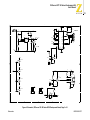
1
Z8F04A28100KIT
®
Z8 Encore! XP 4K Series
Development Kit
User Manual
UM016604-0107
Copyright ©2007 by ZiLOG, Inc. All rights reserved.
www.zilog.com
®
Z8 Encore! XP 4K Series Development Kit
User Manual
ii
This publication is subject to replacement by a later edition. To determine whether a later
edition exists, or to request copies of publications, visit www.zilog.com.
Document Disclaimer
©2007 by ZiLOG, Inc. All rights reserved. Information in this publication concerning the devices,
applications, or technology described is intended to suggest possible uses and may be superseded. ZiLOG,
INC. DOES NOT ASSUME LIABILITY FOR OR PROVIDE A REPRESENTATION OF ACCURACY OF
THE INFORMATION, DEVICES, OR TECHNOLOGY DESCRIBED IN THIS DOCUMENT. ZiLOG
ALSO DOES NOT ASSUME LIABILITY FOR INTELLECTUAL PROPERTY INFRINGEMENT
RELATED IN ANY MANNER TO USE OF INFORMATION, DEVICES, OR TECHNOLOGY
DESCRIBED HEREIN OR OTHERWISE. Except with the express written approval ZiLOG, use of
information, devices, or technology as critical components of life support systems is not authorized. No
licenses or other rights are conveyed, implicitly or otherwise, by this document under any intellectual property
rights.
ZiLOG is a registered trademark of ZiLOG Inc. in the United States and in other countries. Z8, Z8 Encore!, Z8
Encore!, and eZ80 are trademarks or registered trademarks of ZiLOG, Inc. All other product or service names
are the property of their respective owners.
Disclaimer
UM016604-0107
®
Z8 Encore! XP 4K Series Development Kit
User Manual
iii
Revision History
Each instance in the following table reflects a change to this document
from its previous revision. To see more detail, click the appropriate link in
the table.
Date
Revision
Level
Description
Page No
4, 9
December
2006
04
Changed Figure 14 to Figure 2. Updated
schematics.
August
2006
03
Removed Serial from Serial Smart Cable for CR 1
8345.
October
2005
02
Updated schematic to reflect board revision C.
Added 20 MHz clock information, and updated
power supply circuit.
Disclaimer
6, 10, 11
UM016604-0107
®
Z8 Encore! XP 4K Series Development Kit
User Manual
iv
FCC Statement
This device complies with part 15 of the FCC Rules. Operation is subject
to the following two conditions:
1. This device may not cause harmful interference.
2. This device must accept any interference received, including
interference that may cause undesired operation.
Safeguards
The following precautions must be observed when working with the
devices described in this document.
Caution: Always use a grounding strap to prevent damage resulting from
electrostatic discharge (ESD).
Disclaimer
UM016604-0107
®
Z8 Encore! XP 4K Series Development Kit
User Manual
v
Table of Contents
Introduction . . . . . . . . . . . . . . . . . . . . . . . . . . . . . . . . . . . . . . . . . . . . . . . . . .1
Kit Contents . . . . . . . . . . . . . . . . . . . . . . . . . . . . . . . . . . . . . . . . . . . . . . .1
Hardware . . . . . . . . . . . . . . . . . . . . . . . . . . . . . . . . . . . . . . . . . . . . . .1
Software (on CD-ROM) . . . . . . . . . . . . . . . . . . . . . . . . . . . . . . . . . . .1
Documentation . . . . . . . . . . . . . . . . . . . . . . . . . . . . . . . . . . . . . . . . . .2
System/Software Requirements . . . . . . . . . . . . . . . . . . . . . . . . . . . . . . . .3
Supported Host System Configuration . . . . . . . . . . . . . . . . . . . . . . . .3
Installation . . . . . . . . . . . . . . . . . . . . . . . . . . . . . . . . . . . . . . . . . . . . . . . .3
Z8 Encore! XP® 4K Series Development Board . . . . . . . . . . . . . . . . . . . . .4
Features . . . . . . . . . . . . . . . . . . . . . . . . . . . . . . . . . . . . . . . . . . . . . . . . . . .4
Z8 Encore! XP 4K Series MCU . . . . . . . . . . . . . . . . . . . . . . . . . . . . . . . .5
UART with IrDA Endec . . . . . . . . . . . . . . . . . . . . . . . . . . . . . . . . . . . . . .7
Power and Communication Interfaces . . . . . . . . . . . . . . . . . . . . . . . . . . .7
External Interface Headers JP1 and JP2 . . . . . . . . . . . . . . . . . . . . . . . . . .7
Schematic . . . . . . . . . . . . . . . . . . . . . . . . . . . . . . . . . . . . . . . . . . . . . . . . . . . .8
Customer Support . . . . . . . . . . . . . . . . . . . . . . . . . . . . . . . . . . . . . . . . . . . 11
Table of Contents
UM016604-0107
®
Z8 Encore! XP 4K Series Development Kit
User Manual
1
Introduction
ZiLOG’s Z8 Encore! XP® 4K Series MCU is the part of the line of
ZiLOG microcontroller products. The Z8 Encore! MCU Development Kit
(Z8F04A28100KIT) enables users to become familiar with the hardware
and software tools available with this product. This kit consists of the
4 KB version of the Z8 Encore! Development Board that supports and
presents the features of the Z8 Encore! XP 4K Series. This kit allows
you to begin writing application software and contains all supporting
documents.
This manual acquaints you with the Z8 Encore! XP 4K Series MCU
Development Kit and gives instructions on setting up and using the tools
to start building designs and applications.
Kit Contents
The Z8 Encore! XP 4K Series MCU Development Kit contains the
following:
Hardware
•
•
Z8 Encore! XP 4K Series Development board
•
5 V DC power supply
Smart Cable for PC to Z8 Encore! XP 4K Series Development
board (DB9 to six-pin male)
Software (on CD-ROM)
•
•
•
•
Introduction
ZDS II- Z8 Encore!® IDE with ANSI C-Compiler
Sample code
Document browser
Acrobat Reader®
UM016604-0107
®
Z8 Encore! XP 4K Series Development Kit
User Manual
2
Packaging
CD-ROM Containing
Documentation
Power
Supply
Serial Smart Cable
Development
Board
Figure 1. Z8 Encore! XP 4K Series Development Kit Contents
Documentation
•
•
•
Quick Start Guide
Registration card
Z8 Encore! XP 4K Series technical documentation (on CD-ROM):
– Development Kit User Manual
– ZDS II - IDE User Manual
– eZ8 CPU User Manual
– Application Notes
The sample code is installed with ZDS II and resides in the <installation directory>\samples in the disk drive.
Introduction
UM016604-0107
®
Z8 Encore! XP 4K Series Development Kit
User Manual
3
The documentation can be installed with the DemoShield interface or
can be viewed on the CD-ROM using the DemoShield menus and a PDF
reader. A copy of the Acrobat installer is provided on the CD-ROM and
can be installed from the DemoShield install screen. After installing the
documentation, Windows Explorer can be used to select any document to
be viewed with your PDF file viewer.
System/Software Requirements
An IBM PC (or compatible computer) with the following minimum
configuration:
Supported Host System Configuration
•
Win98 Second Edition, WinNT 4.0 Service Pack 6, Win2000 Service
Pack 3, WinXP Professional Service Pack 1
•
•
•
•
•
•
PentiumII/233 MHz processor or higher up to Pentium IV, 2.8 GHz
96 MB RAM or more
25 MB hard disk space or more
Super VGA video adapter
CD-ROM
One or more RS-232 communication ports
Installation
Follow the directions in the Quick Start Guide for software installation
and setup of the Z8 Encore! XP 4K Series Development kit.
Introduction
UM016604-0107
®
Z8 Encore! XP 4K Series Development Kit
User Manual
4
®
Z8 Encore! XP 4K Series
Development Board
The Z8 Encore! XP 4K Series Development board is a development and
prototyping board for the Z8 Encore! XP 4K Series MCU. The board
provides you with a tool to evaluate features of Z8 Encore! XP 4K Series
MCU and to start developing an application before building the hardware.
Figure 2. Z8 Encore! XP 4K Series Development Board
Features
•
•
Z8 Encore!® MCU (28-pin SOIC)
3 LEDs
Z8 Encore! XP® 4K Series Development Board
UM016604-0107
®
Z8 Encore! XP 4K Series Development Kit
User Manual
5
•
•
•
•
•
•
•
•
•
•
RS-232 interface
IrDA transceiver
Two pushbuttons, RESET and TEST
5 VDC power connector
On-Chip Debugger interface
20 MHz Crystal (Y1)
Header for ADC input
Prototyping area
External interface connectors JP1 and JP2
2.7 to 3.6 V operating voltage with 5 V-tolerant inputs
Z8 Encore! XP 4K Series MCU
The Z8 Encore! XP 4K Series MCU is member of a family of ZiLOG
microcontroller products based upon the 8-bit eZ8 core CPU. The Flash
in-circuit programming capability allows for faster development time and
program changes in the field. The eZ8 core CPU is upward compatible
with existing Z8® instructions. The rich peripheral set of the Z8 Encore!
XP 4K Series makes it suitable for a variety of applications including
motor control, security systems, home appliances, personal electronic
devices, and sensors.
Z8 Encore! XP® 4K Series Development Board
UM016604-0107
®
Z8 Encore! XP 4K Series Development Kit
User Manual
6
The Development board contains circuitry to support and present all the
features of the Z8 Encore! XP 4K Series. The main features of the
Z8 Encore! XP 4K Series are:
•
•
•
•
•
•
•
•
•
•
•
•
•
•
•
•
•
eZ8 core CPU
4 KB Flash memory with in-circuit programming capability
1 KB register RAM
5-channel, 10-bit analog-to-digital converter (ADC)
Full-duplex UART
I2C interface (Master Mode only)
Serial Peripheral Interface (SPI)
Infrared Data Association (IrDA)-compliant infrared encoder/decoder
Two 16-bit timers with capture, compare, and PWM capability
Watchdog Timer (WDT) with internal RC oscillator
Eleven (20-pin package) or nineteen (28-pin package) I/O pins
Programmable priority interrupts
On-Chip Debugger (OCD)
Voltage Brown-out Protection (VBO)
Power-on Reset (POR)
2.7–3.6 V operating voltage with 5 V-tolerant inputs
Operating temperatures: 20 °C ±10 °C
For more information on the Z8 Encore!® family of devices, refer to
the product specification (PS0197) available for download at
www.zilog.com.
Z8 Encore! XP® 4K Series Development Board
UM016604-0107
®
Z8 Encore! XP 4K Series Development Kit
User Manual
7
UART with IrDA Endec
The Z8 Encore! XP 4K Series (component U5) contains a fully-functional, high-performance UART with Infrared Encoder/Decoder
(ENDEC). The Infrared Endec is integrated with an on-chip UART allowing easy communication between the Z8 Encore! XP 4K Series and IrDA
transceivers. Infrared communication provides secure, reliable, low-cost,
point-to-point communication between PCs, PDAs, cell phones, printers
and other infrared enabled devices.
Power and Communication Interfaces
Table 1 provides jumper information concerning the shunt status, functions, devices and defaults affected of jumpers JP3 and JP4.
Table 1. Jumpers JP3 and JP4
Jumper
Status
Device Affected
Status
Default
JP3*
OUT
RS-232 interface
Enabled
JP3
IN
RS-232 interface
Disabled
JP4*
OUT
IrDA interface
Enabled
JP4
IN
IrDA interface
Disabled
X
JP5
OUT
U5 RESET/PD0
PD0 (GPIO)
X
JP5
IN
U5 RESET/PD0
RESET when
SW1 pressed
X
* These jumpers must not be OUT at the same time.
External Interface Headers JP1 and JP2
External interface headers JP1 and JP2 are illustrated in the schematic
in Figure 3 and Figure 4 on page 10.
Z8 Encore! XP® 4K Series Development Board
UM016604-0107
®
Z8 Encore! XP 4K Series Development Kit
User Manual
8
Schematics
This section includes schematics for the Z8 Encore! XP 4K Series
Development Board.
Schematics
UM016604-0107
Z8 Encore! XP ® 4K Series Development Kit
User Manual
9
5
4
PA6_nT1OUT
1
2
100
GREEN
R8
D3
PA7_T1OUT
1
R9
SW2
VCC_33V
2
GND
100
YELL
TEST
100K
D
R11
R10
D4
PC3_COUT
1
1
If Module is plugged onto the Dev Platform the local
RS232 interface is disabled by pin 50 of JP2
JP2
connector 2
PB4_ANA7
PC1_ANA5
PB3_ANA3
PB1_ANA1
VCC_33V
PC4
PC7
PC3_COUT
PA6_nT1OUT
GND
PA7_T1OUT
TABLE 1
R12
R13 R16
R17
R22
GPIO
OUT
IN
OUT
IN
IN
OUT
OUT
Analog
Supply
IN
OUT
IN
OUT
OUT
optional
IN
10
RED
PA2
GND
GND
2
100
2
VCC_33V
VCC_33V
3
Note 1:
PB6 and PB7 are dual function pins (GPI O or Analog supply)
R12, R13, R16, and R17 are zero-ohm resistors used in
conjunction with GPIO Control Register s to select function
desired. C21, C22, and C23 are bypass cap acitors that are used
for better noise rejection. U8 is an opt ional filter that can
be used to improve the quality of the Analog Supply. The
development board is shipped configured for Analog Supply.
Table 1 shows the configuratio ns recommended
R7
D2
U8
C21...C23
PA3_CTS0
PA4_RXD0
GND
NOTE 1:
R12
SW1
R19 10K
GND
0
U8
1
GND
VCC_33V
IO
PA0_T0IN_JP
IO
JP5
PB6
3
R22
R20
0
2
R21
0
0
PB1_ANA1
PB2_ANA2
PB3_ANA3
VCC_33V
PA0_T0IN
PA1_T0OUT
GND
PA2
PA3_CTS0
PA4_RXD0
1
2
3
4
5
6
7
8
9
10
PB5_JP
PB1/ANA1
PB2/ANA2
PB3/CLKIN/ANA3
VDD
PA0/T0IN/T0OUT/XIN/
PA1/T0OUT/XOUT
GND
PA2/DE
PA3/CTS0
PA4/RXD0
U5
PB0/ANA0
PC3/COUT/LED
PC2/ANA6/LED
PC1ANA5/CINN/LED
PC0/ANA4/CINP/LED
DBG
RESET/PD0
PA7/T1OUT
PA6/T1IN/T1OUT
PA5/TXD0
PB0_ANA0
PC3_COUT
PC2_ANA6
PC1_ANA5
PC0_ANA4
DBG
PD0
PA7_T1OUT
PA6_nT1OUT
PA5_TXD0
20
19
18
17
16
15
14
13
12
11
C22
VCC_33V
PA0_T0IN
PA1_T0OUT
GND
0.033uF C21 C10
30uF
0.033uF 0.001uF
PA3_CTS0
PA4_RXD0
PA5_TXD0
Z8F1680
R14
0
PB2_ANA2
PB4_ANA7
PB5
PB3_ANA3
SENSE
C23
+
VCC_33V
HEADER 2
EMI Filter
20 pin footprint
U6
-RESET
VCC_33V
1
2
0
PA1_T0OUT_JP
C
PA2
PA3_CTS0
PA4_RXD0
PA5_TXD0
1
2
3
4
5
6
7
8
9
10
11
12
13
14
R16 0
PB2/ANA2
PB4/ANA7
PB5/Vref
PB3/ANA3/CLKIN
PB6(AVDD)
VDD
PA0/T0IN/T0OUTXIN
PA1/T0OUT/XOUT
GND
PB7(AGND)
PA2/DE
PA3/CTS0
PA4/RXD0
PA5/TXD0
PB1/ANA1
PB0/ANA0
PC3/COUT/LED
PC2/ANA6/LED
PC1/ANA5/CINN/LED
PC0/ANA4/CINP/LED
DBG
RESET/PD0
PC7/LED
PC6/LED
PA7/T1OUT
PC5/LED
PC4/LED
PA6/T1IN/T1OUT
1
3
5
7
9
11
13
15
17
19
21
23
25
27
29
31
33
35
A21
37
A22
39
-CS0
41
-CS2
43
D1
45
D3
47
D5
49
D7
51
-MREQ 53
GND
55
-WR
57
-BUSACK 59
3
1
3
PB7
PB0_ANA0
2
2
1
PB1_ANA1
PB2_ANA2
PB3_ANA3
PC0_ANA4
PC1_ANA5
PC2_ANA6
PB4_ANA7
C11
0.001uF
C12
0.001uF
C13
0.001uF
C14
0.001uF
C15
0.001uF
C16
0.001uF
C17
0.001uF
C20
20 MHz
C18
0.001uF
NOTE 2
GND
J2
TABLE 2
Clock Mode
Internal Only
A
R14
R15
none
none
Crystal
0 Ohm
0 Ohm
Ceramic Res
0 Ohm
0 Ohm
External CMOS
none
none
R18
none
C19
none
220K
2 2pF
none
none
none
none
C20
none
22pF
none
none
Y1
none
20MHz
Yes
none
(Use PA0_T0IN
pin on JP2)
Note 2: The XP supports internal, exter nal crystal, external
ceramic resonator, external R/C and external CMOS drive
clock modes. R14, R15, R18, C19, C20 and Y1 are used to
support the clock mode selected. The d evelopment board is
shipped configured for external 20MHz ceramic resonator or
internal clock operation. When using Internal oscilator,
pins 7 and 8 could be used as GPIO port s PA0 and PA1. To do
so install R20 an d R21.
Table 2 shows the recommended clock m ode configurations.
PB0_ANA0
PB1_ANA1
PB2_ANA2
PB3_ANA3
PC0_ANA4
PC1_ANA5
PC2_ANA6
PB4_ANA7
1
3
5
7
9
11
13
15
2
4
6
8
10
12
14
16
HEADER 8X2
3
VCC_33V
A0
A3
VCC_33V
A7
A9
A14
A16
GND
A1
A12
A20
A17
-DIS_FLASH
VCC_33V
A23
-CS1
D0
D2
D4
GND
D6
-IOREQ
-RD
-INSTRD
-BUSREQ
B
A
Title
XP 4K MDS Processor Module. Schematic.
Date:
4
-DIS_232
-DIS_IRDA
GND
HEADER 30x2/SM
Size
B
5
GND
-DIS_IrDA
2
4
6
8
10
12
14
16
18
20
22
24
26
28
30
32
34
36
38
40
42
44
46
48
50
52
54
56
58
60
-TRSTN
-F91_WE
GND
A6
A10
GND
A8
A13
A15
A18
A19
A2
A11
A4
A5
NOTE 1:
C19
PA5_TXD0
connector 1
for
reference
onlyJP1
DBG
220K
Y1
PD0
GND
HEADER 30x2/SM
R18
B
D
C
PB1_ANA1
PB0_ANA0
PC3_COUT
PC2_ANA6
PC1_ANA5
PC0_ANA4
DBG
PD0
PC7
PC6
PA7_T1OUT
PC5
PC4
PA6_nT1OUT
28
27
26
25
24
23
22
21
20
19
18
17
16
15
R17 0
GND
PC2_ANA6
PC0_ANA4
PB2_ANA2
PB0_ANA0
GND
PC5
PC6
PB5_JP
PA0_T0IN_JP
PA1_T0OUT_JP
PA2
2
4
6
8
10
12
14
16
18
20
22
24
26
28
30
32
34
36
38
40
42
44
46
48
50
52
54
56
58
60
28 pin footprint
Z8F1680
R15
0
PB6
PB7
RESET/TEST2
R13
1
3
5
7
9
11
13
15
17
19
21
23
25
27
29
31
33
35
37
39
41
43
45
47
49
51
53
55
57
59
Document Number
Rev
96C0941-001
Friday, September 22, 2006
2
C
Sheet
1
of
2
1
Figure 3. Schematic, Z8 Encore! XP 4K Series MCU Development Board, Page 1 of 2
Schematics
UM016604-0107
Z8 Encore! XP ® 4K Series Development Kit
User Manual
10
5
4
3
2
1
VCC_33V
J1
RXE050
+ C3
C4
0.1uF
D
R23
10K
100/10
-Z_RST
5
VIN
OUT
2
4
SENSE
SHDN
GND
SENSE
VCC_33V
PA5_TXD0
4
C1-
5
C2+
6
C2-
PA5_TXD0
19
C1
0.1uF
V+
3
CONSOLE
GND
P1
C5
0.1uF
V-
7
13
T1IN
T1OUT
17
GND
12
T2IN
T2OUT
8
PA3_CTS0
15
R1OUT
R1IN
16
PA4_RXD0
10
R2OUT
R2IN
9
R1
TXD0
CTS0
RXD0
1
6
2
7
3
8
4
9
5
D
+ C7
C8
680
PA3_CTS0
100/10
3
LT1129-3.3/DD
1
C1+
C6
0.1uF
U7
VCC_33V
2
PA4_RXD0
2
0.1uF
R24
15K
DB9 Female
USER
D1
LED
1
3.3 OK
1
20
EN
SHDN
MAX3222
GND
GND
PWR JACK
VCC
VCC
5V
U1
C2
0.1uF
F1
NC
NC
14
11
18
2
3
1
VCC_33V
GND
R2
10K
C
U3A
14
C
14
74LVC04/SO
U3B
1
-DIS_232
2
3
7
74LVC04/SO
JP3
4
1
2
7
GND
U3C
74LVC04/SO
GND
5
R3
C9
VCC_33V
6
68
330nF
R4
B
7
14
14
R5
10K
U3E
U3D
PA5_TXD0
74LVC04/SO
74LVC04/SO
11
B
U4
2R7
9
-DIS_IRDA
10
IRDA_SD
8
PA4_RXD0
5
VCC
1
LEDA
2
TXD
4
SD
3
RXD
6
GND
7
JP4
7
1
2
T
14
DIS RS232
ZHX1810
0
GND
14
DIS IRDA
GND
U3F
VCC_33V
R6
10K
1
2
3
4
5
12
1
2
3
4
5
74LVC04/SO
13
7
A
TP1
GND
TP2
P2
VCC_33V
GND
1
3
5
A
DBG
INTERFACE
2
4
6
-Z_RST
DBG
DBG
Title
XP 4K MDS Processor Module. Schematic.
Header 3x2
Size
B
Date:
5
4
3
Document Number
Rev
96C0941-001
Friday, September 22, 2006
2
C
Sheet
2
of
2
1
Figure 4. Schematic, Z8 Encore! XP 4K Series MCU Development Board, Page 2 of 2
Schematics
UM016604-0107
®
Z8 Encore! XP 4K Series Development Kit
User Manual
11
Customer Support
If you experience any problems while operating this product, please
check the ZiLOG Knowledge Base:
http://kb.zilog.com/kb/oKBmain.asp
If you cannot find an answer or have further questions, please see the
ZiLOG Technical Support web page:
http://support.zilog.com
Customer Support
UM016604-0107