1
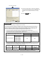
z SAFETY PRECAUTION z
(Always read these instructions before using the products.)
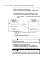
When designing the system, always read the relevant manuals and give sufficient consideration to
safety.
During the exercise, pay full attention to the following points and handle the product correctly.
[EXERCISE PRECAUTIONS]
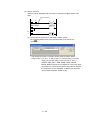
WARNING
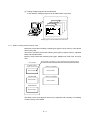
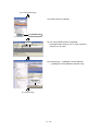
z Do not touch the terminals while the power is on to prevent electric shock.
z Before opening the safety cover, make sure to turn off the power or ensure the safety.
z Do not touch the movable portion.
CAUTION
z Follow the instructor's direction during the exercise.
z Do not remove the module of the demonstration machine or change wirings without permission.
Doing so may cause failures, malfunctions, personal injuries and/or a fire.
z Turn off the power before installing or removing the module.
Failure to do so may result in malfunctions of the module or electric shock.
z When the demonstration machine (such as X/Y table) emits abnormal odor/sound, press "Power
switch" or "Emergency switch" to turn off.
z When a problem occurs, notify the instructor as soon as possible.
REVISIONS
*The textbook number is written at the bottom left of the back cover.
Print date
*Textbook number
Revision
Oct., 2012 SH-081124ENG-A First edition
This textbook confers no industrial property rights or any rights of any other kind, nor does it confer any patent
licenses. Mitsubishi Electric Corporation cannot be held responsible for any problems involving industrial property
rights which may occur as a result of using the contents noted in this textbook.
© 2012 MITSUBISHI ELECTRIC CORPORATION
CONTENTS
INTRODUCTION ······································································································································· (5)
CHAPTER 1
OVERVIEW OF QCPU
1- 1 to 1- 6
CHAPTER 2
SYSTEM CONFIGURATION
2- 1 to 2-20
2.1 Basic System Configuration ············································································································ 2- 1
2.1.1 Device configuration ················································································································· 2- 1
2.1.2 Precautions for system configuration ······················································································· 2- 4
2.2 Connection with GX Works2 ··········································································································· 2- 6
2.2.1 Interface and connection channel ···························································································· 2- 6
2.2.2 Access range from GX Works2 ································································································ 2- 9
2.3 Name and Appearance of CPU······································································································ 2-10
2.4 Memory System Configuration······································································································· 2-13
2.4.1 Universal model QCPU module memory configuration··························································· 2-13
2.4.2 Memory card application ········································································································· 2-15
2.4.3 Handling the memory card ······································································································ 2-16
CHAPTER 3
PERFORMANCE SPECIFICATIONS
3- 1 to 3-16
3.1 Performance Specifications ············································································································ 3- 1
3.2 Device············································································································································· 3-11
CHAPTER 4
4.1
4.2
4.3
BASIC KNOWLEDGE REQUIRED FOR OPERATING GX Works2
4- 1 to 4- 6
Screen Configuration in GX Works2 ······························································································· 4- 1
Basic Operations of Dialog Box ······································································································ 4- 4
Ladder Program Creation Method··································································································· 4- 5
CHAPTER 5
GX Works2 BASIC OPERATIONS (PART 1: SINGLE PROGRAM)
5- 1 to 5-26
5.1 System Configuration of Demonstration Machine··········································································· 5- 1
5.2 Basic Operation 1 (Operation Before Creating Ladder Programs) ················································· 5- 2
5.2.1 Starting up GX Works2············································································································· 5- 2
5.2.2 Selecting programmable controller type and project type (creating a new project) ················· 5- 3
5.2.3 Creating a program··················································································································· 5- 5
5.2.4 Saving a project ························································································································ 5- 9
5.2.5 Saving a project with another name ························································································ 5-11
5.3 Basic Operation 2 (Preparation for CPU Operation)······································································ 5-12
5.3.1 Preparations for starting up CPU ···························································································· 5-12
5.4 Basic Operation 3 (Writing Data to Programmable Controller, Monitoring, Modifying Program) ······ 5-19
5.4.1 Writing data to the CPU··········································································································· 5-19
5.4.2 Reading data from the CPU ···································································································· 5-21
5.4.3 Monitoring ································································································································ 5-22
5.4.4 Modifying a program················································································································ 5-24
(1)
CHAPTER 6 FILE-BASED MANAGEMENT AND PROGRAM EXECUTION MANAGEMENT
6- 1 to 6-14
6.1 File-Based Management ················································································································· 6- 1
6.1.1 Built-in memory and IC memory card······················································································· 6- 3
6.2 Program Execution Management···································································································· 6- 7
6.2.1 Description of program execution type····················································································· 6- 7
6.2.2 Initial execution type program··································································································· 6- 9
6.2.3 Scan execution type program·································································································· 6-10
6.2.4 Standby type program ············································································································· 6-11
6.2.5 Fixed scan execution type program ························································································ 6-12
6.2.6 Executing EI····························································································································· 6-14
CHAPTER 7
GX Works2 BASIC OPERATIONS (PART 2: MULTIPLE PROGRAMS)
7- 1 to 7-14
7.1 Multiple Programs ··························································································································· 7- 1
7.1.1 Creating multiple programs ······································································································ 7- 1
7.1.2 Creating programs for control··································································································· 7- 5
7.1.3 Setting parameters ··················································································································· 7- 7
7.2 Monitor············································································································································ 7-10
7.2.1 Program list monitor ················································································································ 7-10
7.2.2 Monitor function ······················································································································· 7-12
CHAPTER 8
FUNCTIONS OF QCPU
8- 1 to 4-40
8.1 Maintenance and Debug Functions ································································································ 8- 1
8.1.1 Self-diagnostic function ············································································································ 8- 3
8.1.2 System display function············································································································ 8- 5
8.1.3 System protection function ······································································································ 8-10
8.1.4 Password registration function ································································································ 8-10
8.2 Other Functions······························································································································ 8-12
8.2.1 Constant scan function ············································································································ 8-13
8.2.2 Latch function ·························································································································· 8-14
8.2.3 Remote operation function ······································································································ 8-15
8.2.4 Service processing setting······································································································· 8-20
8.3 Comments Storage Function ········································································································· 8-24
8.4 Appropriate Assignment of Device Points······················································································ 8-29
8.5 Using File Register ························································································································· 8-33
8.5.1 Preparation for using file register ···························································································· 8-34
8.5.2 Operation check ······················································································································ 8-38
8.6 Input Response Speed Change ····································································································· 8-39
(2)
CHAPTER 9
PROGRAMMING INTELLIGENT FUNCTION MODULE
9- 1 to 9-20
9.1 Communication with Intelligent Function Module············································································ 9- 1
9.1.1 Various settings with GX Works2 ····························································································· 9- 2
9.1.2 Communications by the intelligent function module device······················································ 9- 4
9.1.3 Communications with the intelligent function module dedicated instruction ···························· 9- 5
9.2 Intelligent Function Module System in Demonstration Machine ····················································· 9- 6
9.2.1 Creating an exercise program ·································································································· 9- 6
9.2.2 Switch setting, parameter setting, and auto refresh setting for the intelligent function module
················································································································································· 9- 9
9.2.3 Operation check and monitor test ··························································································· 9-18
CHAPTER 10
HOW TO USE MULTIPLE CPU SYSTEM
10- 1 to 10-34
10.1 Overview of Multiple CPU System ······························································································ 10- 1
10.2 Difference from Single CPU System ··························································································· 10 -2
10.2.1 Mounting position of QCPU/motion CPU ············································································· 10- 2
10.2.2 I/O number assignment of the multiple CPU system ··························································· 10- 3
10.2.3 Communication between QCPUs and modules··································································· 10- 3
10.2.4 Reset and operation for errors ····························································································· 10- 4
10.3 Communication among each QCPU/Motion CPU in Multiple CPU System ······························· 10- 6
10.3.1 CPU shared memory ············································································································ 10- 6
10.3.2 Communication by auto refresh using CPU shared memory··············································· 10- 9
10.3.3 Communication by auto refresh using multiple CPU high speed transmission area ·········· 10-11
10.3.4 Communications by the multiple CPU instruction and motion dedicated instruction ·········· 10-14
10.4 Starting up Multiple CPU System ································································································· 10-15
10.4.1 Procedure for starting up the multiple CPU system ···························································· 10-15
10.4.2 System configuration of the demonstration machine ·························································· 10-17
10.4.3 Creating a program for CPU No. 1 ······················································································ 10-18
10.4.4 Parameter setting for CPU No. 1························································································· 10-19
10.4.5 Creating a program for CPU No. 2 ······················································································ 10-25
10.4.6 Parameter setting for CPU No. 2························································································· 10-26
10.4.7 Writing data to the CPU······································································································· 10-31
10.4.8 Operation check ·················································································································· 10-33
(3)
APPENDIX
App.- 1 to App.-58
Appendix 1 Instruction Tables ·········································································································· App.- 1
Appendix 1.1 Application instruction····························································································· App.- 2
Appendix 1.2 QCPU Instructions ··································································································· App.-22
Appendix 2 How to Create Ladder Programs with GX Works2 ······················································ App.-23
Appendix 3 Offset/Gain Setting ······································································································· App.-27
Appendix 3.1 Offset/gain setting with GX Works2······································································· App.-27
Appendix 3.2 Offset value and gain value ··················································································· App.-30
Appendix 4 Specifications of the A/D and D/A Converter Modules ················································App.-34
Appendix 4.1 A/D converter module···························································································· App.-34
Appendix 4.2 D/A converter module···························································································· App.-38
Appendix 5 Comparison of Timers and Counters ··········································································· App.-42
Appendix 5.1 Comparison of timers and counters ······································································ App.-42
Appendix 5.2 Comparison of counters ························································································ App.-43
Appendix 6 Setting device initial values ·························································································· App.-44
Appendix 6.1 Setting device memories ······················································································· App.-46
Appendix 6.2 Specifying file names for device initial value ·························································App.-49
Appendix 6.3 Checking the operation of device initial values ·····················································App.-50
Appendix 7 Inline Structured Text ··································································································· App.-51
Appendix 7.1 Editing inline structured text ·················································································· App.-51
Appendix 7.2 Precautions on using the inline structured text ·····················································App.-54
Appendix 8 Battery ·························································································································· App.-55
Appendix 9 Real Number (Floating-point data)··············································································· App.-56
(4)
INTRODUCTION
This textbook explains the programmable controller, the program editing methods
with GX Works2, the sequence instructions and the application instructions for
understanding the MELSEC-Q series programming.
The related manuals are shown below.
(1) QCPU User's Manual (Hardware Design, Maintenance and Inspection)
····························································································· SH-(NA)080483ENG
Explains the hardware.
(2) QnUCPU User's Manual (Function Explanation, Program Fundamentals)
····························································································· SH(NA)-080807ENG
Explains the functions and programming method.
(3) MELSEC-Q/L Programming Manual (Common Instruction)
····························································································· SH(NA)-080809ENG
Explains details of each instruction.
(4) GX Works2 Beginner's Manual (Simple Project)
····························································································· SH(NA)-080787ENG
(5) GX Works2 Version 1 Operating Manual (Common)
····························································································· SH(NA)-080779ENG
(6) GX Works2 Version 1 Operating Manual (Simple Project)
····························································································· SH(NA)-080780ENG
(7) Before Using the Product
··········································································································· BCN-P5782
(8) Digital-Analog Converter Module User's Manual
·····································································································SH(NA)-080054
(9) Before Using the Product
··········································································································· BCN-P5781
(10) Analog-Digital Converter Module User's Manual
·····································································································SH(NA)-080055
(11) MELSEC-Q/L Programming Manual (Structured Text)
·····································································································SH(NA)-080366
(5)
MEMO
(6)
CHAPTER 1 OVERVIEW OF QCPU
The Universal model QCPU is used for a training in this textbook, therefore, "QCPU"
indicates "Universal model QCPU" unless otherwise noted.
QCPU has the following features.
(1) Large number of I/O points can be controlled
The Q-Series CPU module supports the following number of actual I/O points
which are accessible to the I/O modules mounted on the base unit.
(a) Basic model QCPU
• Q00JCPU: 256 points (X/Y0 to FF)
• Q00CPU, Q01CPU: 1024 points (X/Y0 to 3FF)
Up to 2048 points (X/Y0 to 7FF) are supported as the I/O device points
available for refreshing the remote I/O of CC-Link and link I/O (LX, LY) of
the MELSECNET/H.
(b) High Performance model QCPU
One module supports 4096 points (X/Y0 to FFF).
Up to 8192 points (X/Y0 to 1FFF) are supported as the I/O device points
available for the remote I/O stations in the MELSECNET/H remote I/O
network and CC-Link data link.
(c) Process CPU and redundant CPU
One module supports 4096 points (X/Y0 to FFF).
Up to 8192 points (X/Y0 to 1FFF) are supported as the I/O device points
available for the remote I/O stations in the MELSECNET/H remote I/O
network and CC-Link data link.
(d) Universal model QCPU
• Q00UJCPU: 256 points (X/Y0 to FF)
• Q00UCPU, Q01UCPU: 1024 points (X/Y0 to 3FF)
• Q02UCPU: 2048 points (X/Y0 to 7FF)
• Q03UD(E)CPU, Q04UD(E)HCPU, Q06UD(E)HCPU, Q10UD(E)HCPU,
Q13UD(E)HCPU, Q20UD(E)HCPU, Q26UD(E)HCPU: 4096 points (X/Y0
to FFF)
Up to 8192 points (X/Y0 to 1FFF) are supported as the I/O device points
available for the remote I/O stations in the MELSECNET/H remote I/O
network and CC-Link data link.
1-1
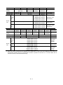
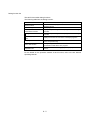
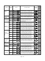
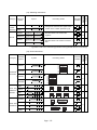
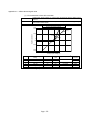
(2) Lineup corresponding to the program capacity
The following table lists the lineup of CPU available for various program
capacity.
CPU module type
Q00(J)CPU
Basic model QCPU
Q01CPU
Q02(H)CPU
High Performance
Q06HCPU
model QCPU
Q12HCPU
Q25HCPU
Q02PHCPU
Q06PHCPU
Process CPU
Q12PHCPU
Q25PHCPU
Q12PRHCPU
Redundant CPU
Q25PRHCPU
Q00U(J)CPU
Q01UCPU
Q02UCPU
Q03UD(E)CPU
Universal model
Q04UD(E)HCPU
QCPU
Q06UD(E)HCPU
Q10UD(E)HCPU
Q13UD(E)HCPU
Q20UD(E)HCPU
Q26UD(E)HCPU
Program capacity
8K steps
14K steps
28K steps
60K steps
124K steps
252K steps
28K steps
60K steps
124K steps
252K steps
124K steps
252K steps
10K steps
15K steps
20K steps
30K steps
40K steps
60K steps
100K steps
130K steps
200K steps
260K steps
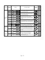
(3) High speed processing
High speed processing has been achieved. (Example: LD instruction)
CPU module type
Basic model QCPU
High Performance
model QCPU
Process CPU
Redundant CPU
Universal model
QCPU
Q00JCPU
Q00CPU
Q01CPU
Q02CPU
Q02HCPU, Q06HCPU, Q12HCPU,
Q25HCPU
Q02PHCPU, Q06PHCPU,
Q12PHCPU, Q25PHCPU
Q12PRHCPU, Q25PRHCPU
Q00UJCPU
Q00UCPU
Q01UCPU
Q02UCPU
Q03UD(E)CPU
Q04UD(E)HCPU, Q06UD(E)HCPU,
Q10UD(E)HCPU, Q13UD(E)HCPU,
Q20UD(E)HCPU, Q26UD(E)HCPU
LD instruction
processing speed
200ns
160ns
100ns
79ns
34ns
120ns
80ns
60ns
40ns
20ns
9.5ns
The high-speed system bus for the MELSEC-Q series base unit has achieved
faster access to an intelligent function module and link refresh with a network
module.
(a) Basic model QCPU
MELSECNET/H link refreshing: 2.2ms/2K words*1
*1: The Q01CPU is used without SB and SW, and the MELSECNET/H network module is
mounted on the main base unit.
1-2
(b) High Performance model QCPU, Process CPU, Redundant CPU or
Universal model QCPU
Access to the intelligent function module: 20μs/word (approximately 7
times*2)
MELSECNET/H link refreshing: 4.6ms/8K words (approximately 4.3
times*2)
*2: These are the values resulted from the following comparison:
•
•
•
Comparing Q02HCPU with Q2ASHCPU-S1
Comparing Q25PHCPU with Q4ARCPU
Comparing Q25PRHCPU with Q4ARCPU
(4) Increased debugging efficiency through high-speed communication with GX
Works2
High-speed communications at maximum 115.2Kbps are available by RS-232
and the time required for writing and reading of programs and monitoring are
reduced. Also, the communication time efficiency of debugging is increased.
In addition, High Performance model QCPUs (except for the Q02CPU), Process
CPUs, Redundant CPUs, and Universal model QCPUs support USB, which
enables high-speed communications at 12Mbps.
(5) AnS/A series I/O modules and special function modules are available
The AnS/A series compatible extension base units (QA1S6B, QA6B, and
QA6ADP+A5B/A6B) enable High Performance model QCPU to use the
AnS/A series I/O modules and special function modules.
* The extension base unit for the A series cannot be used for the Universal
model QCPU.
Main base unit with 5 slots 245mm(9.65inch)
(depth:98mm(3.86inch))
Main base unit with 8 slots 328mm(12.92inch)
Main base unit with 12 slots 439mm(17.28inch)
(7) Connection of up to 7 extension base units
Up to seven extension base units can be connected to the Q series CPU
module.
The whole extension cable length is 13.2m, which enables flexible layout of
base units.
1-3
AnS series
Q series
98mm (3.86inch)
(6) Saved space by downsizing
The installation space for the Q series is reduced by approximately 60%
compared with the AnS series.
(8) Memory extension by memory card*3
The QCPU equips the memory card installing connector so that a memory card
with the capacity of up to 32M byte can be connected. (The 32M-byte memory
card can be connected only when an ATA card is used.)
Installing large-capacity memory cards enables large-capacity files to be
managed, which allows for the comment setting to all data devices and saving
old programs in a memory as correction data.
*3: The Basic model QCPU, Q00(J)CPU, and Q01UCPU do not support memory cards.
POINT
For the High Performance model QCPU, available file register points differs
depending on the function version and serial number.
For details, refer to the QCPU User's Manual Hardware Design, Maintenance
and Inspection.
(9) Automatic writing to standard ROM*4,*5
Parameters and programs of the memory cards can be written to the standard
ROM of the CPU module without GX Works2.
*4: The Basic model QCPU does not support the following functions.
Automatic writing to standard ROM
*5: The Universal model QCPU does not support the following function.
Automatic writing to standard ROM
(10) Forced on and off of external I/O*6
Even when the CPU module is running, forced on and off of external input and
output is available with GX Works2 regardless of the program execution status.
Also, the wiring and operation tests can be conducted without stopping the CPU
module by forcibly turning on or off the I/O.
*6: The Basic model QCPU does not support the following functions.
Forced on and off of external I/O
(11) Remote password setting
When the built-in Ethernet port QCPU, Ethernet module, or serial
communication module is externally accessed, an access to the CPU module
can be controlled by the remote password.
1-4
(12) Remote I/O network of MELSECNET/H*7
A MELSECNET/H remote I/O system can be configured by installing a
MELSECNET/H remote master station.
*7: The Basic model QCPU does not support the following functions.
Remote I/O network of MELSECNET/H
POINT
● The remote password can be set when the built-in Ethernet port QCPU,
Ethernet module, or serial communication module of function version B or
later is used.
● The MELSECNET/H remote I/O network can be implemented when the
MELSECNET/H network module of function version B or later is used.
(13) Supporting the multiple CPU system
The Q series CPU module supports the multiple CPU system.
Multiple CPU system can be configured in combination with CPU modules,
motion CPUs, PC CPU modules, and C Controller module.
For details of the multiple CPU system, refer to the QCPU User's Manual
(Multiple CPU System).
(14) Supporting the redundant power supply system
The redundant power supply system can be configured with a redundant base
unit and redundant power supply modules.
The system can continue operation even when one of the power supply
modules fails, since the other supplies the power.
(15) Direct connection to Ethernet*8
The Built-in Ethernet port QCPU module allows for direct connections to
Ethernet.
For details of the functions, refer to the QnUCPU User's Manual Communication
via Built-in Ethernet Port.
*8: Applicable only to the built-in Ethernet port QCPU.
1-5
MEMO
1-6
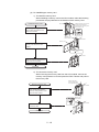
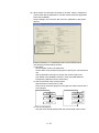
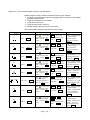
CHAPTER 2 SYSTEM CONFIGURATION
2.1
2.1.1
Basic System Configuration
Device configuration
The following figure shows an actual programmable controller configuration.
Memory card
Battery for QCPU (Q6BAT)
Universal model QCPU
Q7BAT-SET
Q3
DB multiple CPU high speed main base unit
*1
Battery for QCPU (Q7BAT)
Battery holder
Q8BAT-SET
Q8BAT connection cable
Battery for QCPU (Q8BAT)
Extension cable
Power supply module/I/O module/Intelligent function module/Special function module
Q5
Q6
B extension base unit
B extension base unit
Figure 2.1 Universal model QCPU module configuration (When Q3DB is used)
*1: The following bases are also available for the Universal model QCPU:
• Q3B type main base unit
• Q3RB type redundant power main base unit
• Q3SB type slim type main base unit
2-1
Base Unit
Extension base unit
(requiring a power
supply module)
Power supply
CPU
CPU
Power supply
Q33B
Power supply
Q35B
Q38B
Q312B
Power supply
Power supply
Power supply
With 12
I/O modules
CPU
With eight
I/O modules
Power supply
With five
I/O modules
CPU
With three
I/O modules
Power supply
Main base unit
(Not requiring a
power supply module)
Q52B
(For two modules)
Q63B
Q55B
Q65B
Q68B
Q612B
Power supply
CPU
With 12
I/O modules
CPU
With eight
I/O modules
Power supply
Multiple CPU high speed main base unit
Q38DB
Q312DB
Power supply
CPU
CPU
With five
I/O modules
Power supply
With three
I/O modules
CPU
With two
I/O modules
Power supply
Slim type main base unit
Q32SB
Q33SB
Q35SB
The main roles of the base unit are; fixing the power supply module, CPU module,
and I/O modules, supplying 5VDC power from the power supply module to the CPU
module and I/O modules, and transmitting the control signals to each module.
2-2
Power Supply Module
Module name
Q61P
Q62P
Q63P
Q64PN
Q61P-D
Q61SP
Input
100V to 240VAC
100V to 240VAC
24VDC
100V to 240VAC
100V to 240VAC
100V to 240VAC
Output
5VDC 6A
5VDC 3A, 24VDC 0.6A
5VDC 6A
5VDC 8.5A
5VDC 6A
5VDC 2A
CPU Module
CPU type
Program capacity
(maximum)
Basic instruction
processing speed
Q00UJCPU
Q00UCPU
Q01UCPU
Q02UCPU
Q03UD(E)CPU
Q04UD(E)HCPU
Q06UD(E)HCPU
Q10UD(E)HCPU
Q13UD(E)HCPU
Q20UD(E)HCPU
Q26UD(E)HCPU
10K steps
10K steps
15K steps
20K steps
30K steps
40K steps
60K steps
100K steps
130K steps
200K steps
260K steps
120ns
80ns
60ns
40ns
20ns
Maximum I/O points for
connecting to a
programmable controller
256 points
1024 points
1024 points
2048 points
4096 points
9.5ns
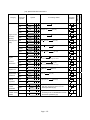
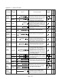
I/O Module
I/O points
Output module
Input module
Format
120VAC
240VAC
24VDC (positive
common)
24VDC
(high-speed input)
24VDC (negative
common)
5/12VDC
Contact output
Independent
contact output
Triac output
Transistor output
(sink)
Transistor output
(source)
I/O mixed
8 points
16 points
32 points
64 points
{
{
-
-
-
-
{
{
{
{
-
-
-
-
{
{
-
-
{
{
{
-
{
-
{
-
-
-
-
{
-
-
{
{
{
{
-
{
{
-
{
-
{
-
2-3
2.1.2
Precautions for system configuration
This section explains restrictions for configuring the system with the Q-series CPU
module.
(1) Number of mountable modules
(a) The number of mountable modules and supported functions are restricted
depending on the module type.
[When the Universal model QCPU is used]
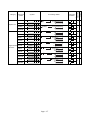
Product name
Maximum number of
modules/units per system
Model name
CC-Link IE controller
*1
network module
MELSECNET/H network
module
Q series Ethernet
interface module
Q series CC-Link system
master/local module
Interrupt module
GOT (Graphic Operation
Terminal)
• QJ71GP21-SX
• QJ71GP21S-SX
• QJ71LP21
• QJ71BR11
• QJ71LP21-25
• QJ71LP21S-25
• QJ71LP21G
• QJ71NT11B
• QJ71E71
• QJ71E71-B2
• QJ71E71-B5
• QJ71E71-100
• QJ61BT11
• QJ61BT11N
• QI60
GOT1000 Series (for bus connection
*7
only)
*2, *3
Up to 4 modules
*3
Up to 4 modules
*4, *5
No restriction
*6
Only 1 module
Up to 5 units
*1: Only the CC-Link IE controller network module with the serial number (first five digits) of
"09042" or later can be used.
*2: The number is a total of the CC-Link IE controller network module and MELSECNET/H
network module.
*3: One module is mountable to the one system of the Q00UJCPU, Q00UCPU, and the
Q01UCPU, and two modules for the Q02UCPU.
*4: Available in modules with function version B or later.
*5: One CPU module can control the following number of modules by setting CC-Link
network parameters in GX Works2.
• Q00UJCPU, Q00UCPU, Q01UCPU: up to 2 modules
• Q02UCPU: up to 4 modules
• Q03UD(E)CPU, Q04UD(E)HCPU, Q06UD(E)HCPU, Q10UD(E)HCPU,
Q13UD(E)HCPU, Q20UD(E)HCPU, Q26UD(E)HCPU: up to 8 modules
There is no restriction on the number of modules when the parameters are set with the
CC-Link dedicated instructions.
For the CC-Link system master/local modules whose parameters can be set by the
dedicated instructions, refer to the CC-Link System Master/Local Module User's Manual.
*6: This number indicates the number of interrupt modules with no interrupt pointer setting.
There is no restriction on the number of modules for the interrupt modules with the
interrupt pointer setting.
*7: For the available GOT models, refer to the GOT1000 Series Connection Manual.
2-4
(b) For the GOTs, the GOT1000 series are available (however,
Q-mode-compatible operating system and communication driver must be
installed).
The Q series bus connection interface module is required for the bus
connection.
The GOT800 series, A77GOT, and A64GOT cannot be used.
The GOT900 series do not support the Universal model QCPU.
2-5
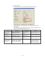
2.2
2.2.1
Connection with GX Works2
Interface and connection channel
In the Q series, flexible and wide methods are available for connecting the CPU and
GX Works2.
For details, refer to the GX Works2 Operating Manual.
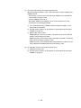
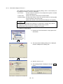
GX Works2 has the following two items about the "connection destination".
(1) Specification of I/F
PC side I/F or PLC side I/F
(2) Other station setting and network route
Other Station Setting, Network Communication Route, Co-existence Network
Route
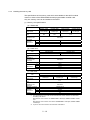
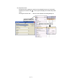
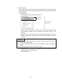
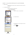
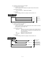
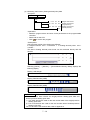
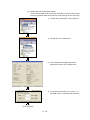
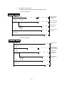
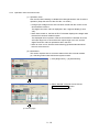
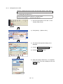
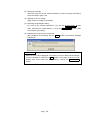
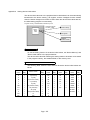
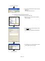
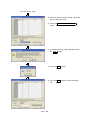
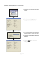
The following explains each item of the Transfer Setup screen.
1)
2)
7)
3)
8)
9)
4)
10)
5)
6)
1) PC side I/F
Select the type of the interface on the personal computer side.
Double-click each interface to set the details.
2) PLC side I/F
Select the module on the programmable controller side to be connected
with the peripheral device.
Double-click each module to set the details.
2-6
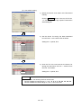
3) Other Station Setting
Specify the host station or other station.
Double-click each icon to set the details.
• No Specification
Select this to access the programmable controller CPU which is directly
connected to a personal computer.
• Other Station (Single Network)
Select this to access the programmable controller CPU on other station
via only one type of network (including a multi-tier system) such as
CC-Link, MELSECNET/10(H), CC-Link IE controller network, Q series
C24 module and Ethernet.
Since Ethernet is recognized as equivalent to CC-Link IE controller
network and MELSECNET/10(H), select "Single Network" for a mixed
system in which Ethernet, CC-Link IE controller network, and
MELSECNET/10(H) are configured.
• Other Station (Co-existence Network)
Select this to access the programmable controller CPU on other station
via two types of network.
This means the system which consists of two different networks, such as
from MELSECNET/10(H) to CC-Link module or from Q series C24
module to MELSECNET/10(H).
4) Network Communication Route
Select the network type, network number, station number, and the start I/O
number of the network that is routed at an access to the programmable
controller CPU on other station. The setting items differ according to the
selected network type.
5) Co-existence Network Route
Select the network type, network number, station number, and the start I/O
number of the network to be accessed. The setting items differ according to
the selected network type.
6) Target System
In the multiple CPU system, specify the CPU number to be accessed.
7)
Connection Channel List button
Displays a list of the types of the connection destination.
The connection route can be selected from the list.
8)
PLC Direct Coupled Setting button
This function is useful to change the station specification from "Other
Station" to "No Specification".
9)
Connection Test button
Tests if the target programmable controller CPU set on the Transfer Setup
screen can be accessed properly.
If the test is successful, the model of the target programmable controller
CPU module is displayed in the PLC Type column.
2-7
10) System Image button
Displays the connection route in an illustration.
2-8
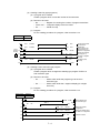
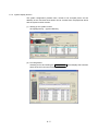
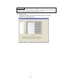
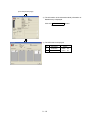
2.2.2
Access range from GX Works2
The seamless communication is established among CC-Link IE, Ethernet,
MELSECNET/H, and CC-Link of the Q series.
GX Works2 can access a programmable controller via various networks.
Ethernet
MELSECNET/H, CC-Link IE
CC-Link
(1) Access example via Ethernet, CC-Link IE, MELSECNET/H, and CC-Link
The request source GX Works2 can access up to two target stations.
Network 2 to 7
Request source
GX Works2
(Personal computer)
QCPU
Network 1
(Ethernet)
Relay
station 1
QCPU
CC-Link IE
MELSEC
NET/H
Relay
station 7
Network 8
CC-Link IE
MELSECNET/H
QCPU
Target
station 1
CC-Link
QCPU
Target
station 2
(2) Access example via CC-Link IE, MELSECNET/H, and CC-Link
The request source GX Works2 can access up to two target stations.
Request source
GX Works2
(Personal computer)
CPU port
Network 2 to 7
QCPU
Connected
programmable
controller
Network 1
CC-Link IE
MELSECNET/H
QCPU
Relay
station 1
QCPU
CC-Link IE
MELSEC
NET/H
Relay
station 7
QCPU
Network 8
CC-Link IE
MELSECNET/H
Target
station 1
CC-Link
2-9
QCPU
Target
station 2
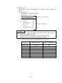
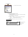
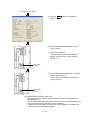
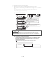
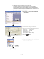
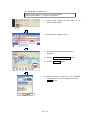
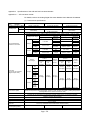
2.3
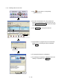
Name and Appearance of CPU
This section explains part names and setting of the module.
Q06UDHCPU
1)
2)
MODE
RUN
ERR.
USER
BAT.
BOOT
3)
Q06UDHCPU
9)
4)
5)
6)
7)
10)
13)
PULL
USB
11)
12)
RS-232
8)
When opening the cover, put
your finger here.
14)
15)
18)
17)
16)
2 - 10
No.
Name
1)
Module fixing hook
2)
MODE LED
3)
RUN LED
4)
ERR. LED
5)
USER LED
6)
BAT. LED
7)
BOOT LED
8)
Serial number display
Memory card EJECT
button
Memory card installing
connector
9)
10)
Application
Hook used to fix the module to the base unit (Single-operation installation)
Indicates the mode of the CPU module
On : Q mode
Flash : Device test with conditions is in process.
Forced on and off function for external I/O is in process.
CPU module change function with memory card is in process.
Indicates the operation status of the CPU module
On : During operation with the RUN/STOP/RESET switch set to "RUN"
Off : During stop with the RUN/STOP/RESET switch set to "STOP"
When an error which stops operation is detected
Flash : Parameters or programs are written when the RUN/STOP/RESET switch is
set to "STOP", then the RUN/STOP/RESET switch is set from "STOP" to
"RUN"
To turn on the RUN LED after writing the program, perform the following
operations.
• Set the RUN/STOP/RESET switch "RUN" → "STOP" → "RUN".
• Reset the CPU module with the RUN/STOP/RESET switch.
• Power on the programmable controller again.
To turn on the RUN LED after writing the parameters, perform the
following operations.
• Reset the CPU module with the RUN/STOP/RESET switch.
• Power on the programmable controller again.
(When the RUN/STOP/RESET switch is set to "RUN" → "STOP" →
"RUN" after the parameters are changed, network parameters and
intelligent function module parameters are not updated.)
On : When a self-diagnosis error which does not stop the operation except a
battery error is detected
(When operation is set to be continued at an error detection in the
parameter setting)
Off : Normal
Flash : When an error which stops operation is detected
When the reset operation becomes valid with the RUN/STOP/RESET
switch
On : When the annunciator is (F) turned on
Off : Normal
On (yellow)
: When a battery error occurs due to a battery voltage drop of the
memory card
Flash (yellow) : When a battery error occurs due to a voltage drop of the CPU
module battery
On (green)
: Turns on for five seconds when the restoration of the data backed
up to the standard ROM by the latch data backup is completed.
Flash (green) : Flashes when the backup of the data to the standard ROM by the
latch data backup is completed.
Off
: Normal
On : When the boot operation is started
Off : When the boot operation is not being performed
Displays the serial number printed on the rating plate.
Used to eject the memory card from the CPU module
Connector used to install a memory card to the CPU module
2 - 11
No.
Name
*1
11)
USB connector
12)
RS-232 connector
13)
RUN/STOP/RESET
*2
switch
14)
15)
Module fixing screw hole
Module fixing projection
16)
Battery connector pin
17)
18)
Battery
Module mounting lever
*1
Application
Connector for connection with a USB-compatible peripheral device (Connector type
miniB)
Can be connected with a USB-dedicated cable.
Connector for connection with a peripheral device
Can be connected with a RS-232 connection cable (QC30R2).
RUN : Executes sequence program operation.
STOP : Stops sequence program operation.
RESET : Executes hardware reset, operation error reset, and operation initialization
etc.
Hole for the fixing screw to the base unit (M3 × 12 screw)
Projection used to secure the module to the base unit
Pins used to connect battery lead wires
(Lead wires are disconnected from the connector at the shipping to prevent the
battery from consuming.)
Backup battery for the standard RAM and back-up power function
Lever used to mount the module to the base unit
*1: When connecting a cable to the RS-232 connector or USB connector at all times, clamp the cable to prevent a poor connection,
moving, and disconnection by unintentional pulling.
The Q6HLD-R2 type connector disconnection prevention holder is provided as a clamp for the RS-232 connector.
CPU module
RS-232 cable
Q6HLD-R2
Fixing screw
*2: Operate the RUN/STOP/RESET switch with a fingertip.
To prevent the switch from damage, do not use any tool such as screw driver.
2 - 12
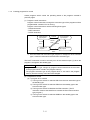
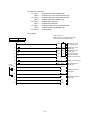
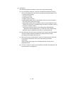
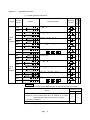
2.4
Memory System Configuration
2.4.1
Universal model QCPU module memory configuration
The memory of universal model QCPU consists of the following block
configurations.
Program memory
(program cache memory)
RAM
Parameter
Program
Parameter
Program
Device comment
Device initial value
Device comment
Device initial value
File register
Local device
Standard
ROM
Parameter
Program
Device comment
Device initial value
Sampling
trace file
Memory card
ROM
*1
Programmable
controller user data
CPU module
Storage file used in latch
data backup function
Parameter
Program
Device comment
Device initial value
File register
File used in
SP.DEVST/S.DEVLD function
Standard
RAM *2
File register
Local device
Sampling
trace file
Module error
collection file
*1: A memory card cannot be used for Q00UJCPU, Q00UCPU, and Q01UCPU.
*2: Q00UJCPU has no standard RAM.
• Program memory:
A memory for storing programs and parameters for CPU module
operation
A program operation is executed by transferring a program stored in
the program memory to the program cache memory.
• Program cache memory: A memory for operating programs
A program operation is executed by transferring a program stored in
the program memory to the program cache memory.
• Standard RAM:
A memory for using file registers, local devices, and sampling trace
files without a memory card
Using the standard RAM as the file registers enables the
high-speed access as well as data registers.
The standard RAM is also used for storing the module error
collection file.
• Standard ROM:
A memory for storing data such as parameters and programs
• Memory card (RAM):
A card for storing the file register, local device, device initial value,
sampling trace file, and device comments with the parameters and
program
• Memory card (ROM):
A Flash card for storing parameters, programs, and file registers.
An ATA card stores parameters, programs, and the programmable
controller user data (general-purpose files).
2 - 13
POINT
Secure backup by long-term storage
Programs and parameter files are automatically backed up to the program
memory (Flash ROM) which does not require a battery backup. This prevents a
loss of the program and parameter data due to the flat battery.
The battery backup time is also reduced significantly.
In addition, the important data (such as device data) can be backed up to the
standard ROM to prevent a loss of the data due to the flat battery in case of
consecutive holidays.
The backup data is restored automatically when the power is turned on next
time.
CPU built-in memory
Program memory
(Flash ROM)
Write programs
Programming
tool
Program
cache memory
(SRAM)
No battery
backup
needed!
For program
execution
Device data
Backup
Latch data
Device memory execution
Backup
condition is
file
ON
(Standard ROM)
File register
(Standard RAM)
2 - 14
No battery
required
for data
protection
2.4.2
Memory card application
A QCPU equips a built-in memory as standard for storing parameters and programs,
therefore, the programs can be executed without a memory card.
The memory cards are required for the situations in the table below.
*: A memory card cannot be used for Q00UJCPU, Q00UCPU, Q01UCPU.
(1) SRAM card
File registers in the SRAM card can be written or read by the sequence
program.
The SRAM card is used when:
• the number of file registers exceeds the standard RAM capacity, or
• the sampling trace function is used.
When file registers are stored to the SRAM card, they can be written or read by
the sequence program up to 4086K points.
(2) Flash card
Write data with GX Works2 and read it by the sequence program. (Data can
only be read by the sequence program.)
Use the Flash card when changing the data is unnecessary.
File registers can be stored up to 2039K points.
(3) ATA card
An ATA card is used for programmable controller user data (general-purpose
data).
Programmable controller user data of an ATA card can be accessed by the file
access instruction (such as the SP.FWRITE instruction) in a sequence program
through a CSV format or binary format.
2 - 15
2.4.3
Handling the memory card
The specifications of the memory card which are available for the QCPU module
conform to those of the JEIDA/PCMCIA small programmable controller card.
Only one memory card can be installed to the QCPU.
(1) Memory card specifications
(a) SRAM card
Item
Memory capacity
after format
Storable number of
files
Number of
insertions and
removals
H
External
W
dimensions
D
Weight
Type
Q2MEM-2MBS
Q3MEM-4MBS
Q2MEM-1MBS
1011.5K byte
2034K byte
255
287
Q3MEM-8MBS
4078K byte
8172K byte
319
5000 times
45mm
74mm
42.8mm
3.3mm
15g
8.1mm
30g
31g
(b) Flash card
Item
Memory capacity
Storable number of
files
Number of
insertions and
removals
Number of writings
H
External
W
dimensions
D
Weight
Type
Q2MEM-2MBF
2035K byte
Q2MEM-4MBF
4079K byte
288
5000 times
100000 times
45mm
42.8mm
3.3mm
15g
(c) ATA card
Item
Memory capacity
after format
Storable number of
files
Number of
insertions and
removals
Number of writings
H
External
W
dimensions
D
Weight
Q2MEM-8MBA
7982K byte
*1
Type
*2
Q2MEM-16MBA
15982K byte
*1
Q2MEM-32MBA
31854K byte
*2
512
5000 times
1000000 times
45mm
42.8mm
3.3mm
15g
*1: The capacity of the ATA cards with the manufacturer control number E or earlier after
formatting is as follows.
Manufacturer control number E: Q2MEM-8MBA: 7948K byte, Q2MEM-16MBA: 15948K
byte
Manufacturer control number E or earlier: Q2MEM-8MBA: 7940k byte, Q2MEM-16MBA:
15932K byte
*2: Up to 511 files can be stored in the Universal model QCPU.
2 - 16
(2) When using the memory card in the purchased status
(a) Install the enclosed battery.
• SRAM card battery
Type
Item
Classification
Initial voltage (V)
Nominal current
(mAh)
Battery life when
stored
Battery life when
used
Application
Q2MEM-BAT
Q3MEM-BAT
3.0
Manganese dioxide lithium primary
battery
3.0
48
550
Graphite fluoride lithium primary battery
Actually 5 years (room temperature)
Refer to the QCPU User's Manual Hardware Design, Maintenance and
Inspection
Power failure backup for SRAM card
Power failure backup for SRAM card
For Q2MEM-1MBS/Q2MEM-2MBS
For Q3MEM-4MBS/Q3MEM-8MBS
(b) Since the memory card is not formatted in the initial setting, use the card
after formatting in GX Works2.
Formatting is unnecessary for Flash cards.
2 - 17
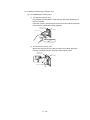
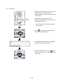
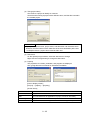
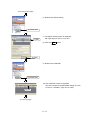
(3) Installing and removing a memory card
(a) For Q2MEM type memory card
1) To install the memory card
Pay attention to the direction of the memory card when installing it to
the CPU module.
Insert the memory card securely into the connector until the projection
of the memory card EJECT button appears.
Memory card
EJECT button
CPU module
Memory card
* Check the insert direction.
( mark)
2) To remove the memory card
When removing the memory card from the CPU module, press the
memory card EJECT button and pull out the memory card.
Memory card
EJECT button
CPU module
Push
Memory card
2 - 18
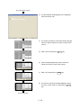
(b) For Q3MEM type memory card
1) To install the memory card
When installing a memory card to the CPU module, follow the following
procedures and pay attention to the direction of the memory card.
Install the memory card
Slightly bend the center of a lid
to make space between a
projection and a mounting hole
and remove the lid.
CPU module
Turn OFF power supply of the
CPU module and remove a lid
of the CPU module.
Projection
MEMORY card
EJECT button
CPU module
Memory card
Install a memory card to a
memory card slot of the CPU
module.
* Check the insert direction.
( mark)
CPU module
Install the memory card protective
cover to the CPU module.
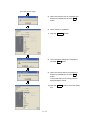
Completed
2) To remove the memory card
When removing the memory card from the CPU module, remove the
memory card protective cover and press the EJECT button and pull out
the memory card.
Remove the cover ,
pressing fixing claws
on the top and bottom.
Remove a memory card
CPU module
Turn OFF power supply of the
CPU module and remove a
memory card protective cover
from the CPU module.
Memory card
EJECT button
Push
Press the EJECT button to eject
a memory card.
Completed
2 - 19
CPU module
(c) To remove the memory card while the power is on
When removing the memory card, confirm that special relays "SM604" and
"SM605" are off.
• The memory card cannot be removed when "SM604" is on because the
CPU module is using the card.
• Turn off "SM605" when it is on.
When both "SM604" and "SM605" are off, remove the memory card
according to the following procedure.
1) Turn on the special relay "SM609" with the sequence program or the
device test of GX Works2.
2) Use the monitor function of GX Works2 to check that the special relay
"SM600" is turned off.
3) Remove the memory card.
SM600 (Memory card can be used): The system is turned on when the
memory card is ready to be used.
SM604 (memory card is being used): The system is turned on when the
CPU module is using the memory card.
SM605 (memory card installation/removal prohibited): Turned on by the
user to disable a installation/removal of the memory card.
(d) To install the memory card while the power is on
1) Install the memory card.
2) Use the monitor function of GX Works2 to check that the special relay
"SM600" is turned on.
2 - 20
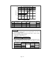
CHAPTER 3 PERFORMANCE SPECIFICATIONS
3.1
Performance Specifications
The following table lists the performance specifications of the Universal model
QCPU.
(1) Q00UJCPU, Q00UCPU, Q01UCPU, Q02UCPU, Q03UD(E)CPU
Universal model QCPU
Item
Control method
I/O control mode
Program
language
Sequence control
language
Process control language
LD X0
Processing
speed
(sequence
MOV D0 D1
instruction)
Processing
Tracking execution time
speed
(redundant (increased scan time)
function)
Constant scanning
(function for keeping regular scan time)
Q00UJCPU
Q00UCPU
240ns
Q03UDCPU
Q03UDECPU
160ns
120ns
80ns
40ns
0.5 to 2000ms (setting available in 0.5ms unit) (setting by parameters)
*1 *2
Program memory
(drive 0)
Memory card (RAM)
(drive 1)
10K steps
(40K byte)
15K steps
(60K byte)
20K steps
(80K byte)
30K steps
(120K byte)
40K byte
60K byte
80K byte
120K byte
Capacity of the installed
memory card (8M byte max.)
Capacity of the installed
memory card
(Flash card: 4M byte max.,
ATA card: 32M byte max.)
-
Memory card (ROM)
(drive 2)
Standard RAM
(drive 3)
Standard ROM
(drive 4)
QCPU
standard
memory
CPU
Multiple
shared
*3 CPU high
memory
speed
transmission
area
Q02UCPU
Stored program repeat operation
Refresh mode
(Direct access I/O is available by specifying direct access I/O (DX, DY).)
Relay symbol language, logic symbolic language, MELSAP3 (SFC),
MELSAP-L, function block, and structured text (ST)
120ns
80ns
60ns
40ns
20ns
Program capacity
Memory
*1
capacity
Q01UCPU
-
-
128K byte
192K byte
256K byte
512K byte
1024K byte
-
8K byte
-
32K byte
*1: The size unit of the files stored in the memory area differs depending on the CPU module.
For details, refer to the QnUCPU User's Manual (Function Explanation, Program Fundamentals).
*2: The maximum number of executable sequence steps is obtained by the following formula.
(Program capacity) - (File header size (Default: 34 steps))
For details of the program capacity and files, refer to the QnUCPU User's Manual (Function Explanation, Program
Fundamentals).
*3: Data in the CPU shared memory is not latched.
Data in the CPU shared memory is cleared when the programmable controller is powered on or the CPU module is
reset.
3-1
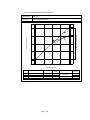
Universal model QCPU
Item
Max. number of
files stored
Q00UJCPU
Program memory
Memory card
(RAM)
Flash
Memory
card
card
ATA
(ROM)
card
Standard RAM
Standard ROM
Number of times of writing data into
the program memory
Number of times of writing data into
the standard ROM
Number of I/O device points
(number of usable points on
program)
Number of I/O points
(number of points accessible to the
actual I/O module)
Internal relay [M]
-
64
124
319 (when the Q3MEM-8MBS
is used)
-
288
-
511
3 files (each one of the following files: file register file, local
device file, and sampling trace file)
128
256
*4
Max. 100000 times
*5
Max. 100000 times
8192 points (X/Y0 to 1FFF)
256 points
(X/Y0 to FF)
*6
1024 points
(X/Y0 to 3FF)
2048 points
(X/Y0 to 7FF)
4096 points
(X/Y0 to FFF)
8192 points by default (M0 to 8191) (changeable)
8192 points by default (L0 to 8191) (changeable)
*6
8192 points by default (B0 to 1FFF) (changeable)
2048 points by default (T0 to 2047) (changeable) (sharing of low- and
high-speed timers)
The low- and high-speed timers are specified by the instructions.
The measurement units of the low- and high-speed timers are set up by
parameters.
(Low-speed timer: 1 to 1000ms, 1ms unit, 100ms by default)
(High-speed timer: 0.1 to 100ms, 0.1ms unit, 10ms by default)
0 point by default (sharing of the low- and high-speed retentive timers)
(changeable)
The low- and high-speed retentive timers are specified by the instructions.
The measurement units of the low- and high-speed retentive timers are set up
by parameters.
(Low-speed retentive timer: 1 to 1000ms, 1ms unit, 100ms by default)
(High-speed retentive timer: 0.1 to 100ms, 0.1ms unit, 10ms by default)
Link relay [B]
*6
Retentive timer [ST]
*6
*6
Counter [C]
Normal counter, 1024 points by default (C0 to 1023) (changeable)
*6
Data register [D]
12288 points by default (D0 to 12287) (changeable)
Extended data register [D]
-
*6
Link register [W]
*6
Annunciator [F]
Link special register
*6
[SW]
-
0 point by default (changeable)
2048 points by default (F0 to 2047) (changeable)
*6
Link special relay [SB]
0 point by default (changeable)
8192 points by default (W0 to 1FFF) (changeable)
Extended link register [W]
Edge relay [V]
Q03UDCPU
Q03UDECPU
Q02UCPU
-
Latch relay [L]
Number
of
device
points
Q01UCPU
32
*6
Timer [T]
Q00UCPU
2048 points by default (V0 to 2047) (changeable)
*6
2048 points by default (SB0 to 7FF) (changeable)
2048 points by default (SW0 to 7FF) (changeable)
*4: A single writing operation may not be counted as one.
The number of writing into the program memory can be checked with the special register (SD682 and SD683).
*5: A single writing operation may not be counted as one.
The number of writing into the standard ROM can be checked with the special register (SD687 and SD688).
*6: The number of points can be changed within the setting range.
3-2
Universal model QCPU
Item
Q00UJCPU
Standard
RAM
[R]
-
SRAM
card
(1M byte)
SRAM
card
(2M byte)
SRAM
card
(4M byte)
SRAM
card
(8M byte)
Flash card
(2M byte)
Number
of
device
points
Flash card
(4M byte)
File
register
*7
Standard
RAM
[ZR]
-
Q00UCPU
Q01UCPU
Q02UCPU
Q03UDCPU
Q03UDECPU
32768 points
(R0 to 32767)
Max. 98304
32768 points (R0 to 32767)
points by
Max. 65536 points by block switching
block
switching
Max. 517120 points by block
switching in units of 32768
points (R0 to 32767)
Max. 1041408 points by block
switching in units of 32768
points (R0 to 32767)
Max. 2087936 points by block
switching in units of 32768
points (R0 to 32767)
Max. 4184064 points by block
switching in units of 32768
points (R0 to 32767)
Max. 1041408 points by block
switching in units of 32768
points (R0 to 32767)
Max. 2087936 points by block
switching in units of 32768
points (R0 to 32767)
98304 points
(ZR0 to
98303)
65536 points (ZR0 to 65535)
Block
Block switching not required
switching not
required
SRAM
card
(1M byte)
-
517120 points (ZR0 to
517119), Block switching not
required
SRAM
card
(2M byte)
-
1041408 points (ZR0 to
1041407), Block switching not
required
SRAM
card
(4M byte)
SRAM
card
(8M byte)
-
-
Flash card
(2M byte)
-
Flash card
(4M byte)
-
*7: When a Flash card is used, only reading is possible. ATA cards cannot be used.
3-3
2087936 points (ZR0 to
2087935), Block switching not
required
4184064 points (ZR0 to
4184063), Block switching not
required
1041408 points (ZR0 to
1041407), Block switching not
required
2087936 points (ZR0 to
2087935), Block switching not
required
Universal model QCPU
Item
Q00UJCPU
*8
Step relay [S]
Index register/
Standard devise register [Z]
Index register [Z]
(32-bit indexing specification
of ZR device)
Pointer [P]
Number
of
device
points
Interrupt pointer [I]
Special relay [SM]
Special register [SD]
Function input [FX]
Function output [FY]
Function register [FD]
Number of device tracking words
Link direct device
Intelligent function module device
Specifications
of built-in
Ethernet port
CPU
*10
module
Data transmission speed
Communication mode
Transmission method
Max. distance between
hub and node
Max.
10BASE-T
number of
connectable
10BASE-T
nodes
Q00UCPU
Q01UCPU
Q02UCPU
Q03UDCPU
Q03UDECPU
*9
8192 points (S0 to 8191) (the number of device points is fixed.)
Max. 20 points (Z0 to 19)
Max. 10 points (Z0 to 18)
(Index register (Z) is used in double words.)
-
4096 points (P0 to 4095),
512 points (P0 to 511),
The available ranges of the local
The available ranges of the local
pointers and common pointers can
pointers and common pointers can be
be set by parameters.
set by parameters.
256 points (I0 to 255)
128 points (I0 to 127)
The constant cyclic interval of
The constant cyclic interval of system
system interrupt pointers I28 to 31
interrupt pointers I28 to 31 can be set
can be set by parameters.
by parameters.
(0.5 to 1000ms, 0.5ms unit)
(0.5 to 1000ms, 0.5ms unit)
Default value I28: 100ms, I29:
Default value I28: 100ms, I29: 40ms,
40ms, I30: 20ms, I31: 10ms
I30: 20ms, I31: 10ms
2048 points (SM0 to 2047) (the number of device points is fixed.)
2048 points (SD0 to 2047) (the number of device points is fixed.)
16 points (FX0 to F) (the number of device points is fixed.)
16 points (FY0 to F) (the number of device points is fixed.)
5 points (FD0 to 4) (the number of device points is fixed.)
Device for accessing the link device directly
Dedicated to CC-Link IE controller network and MELSECNET/H
Specified form: J\X, J\Y, J\W, J\B, J\SW, J\SB
Device for accessing the buffer memory of the intelligent function module
directly
Specified form: U\G
100/10Mbps
Full-duplex/Half-duplex
Base band
-
*11
Number of connections
-
*8:
*9:
100m
Cascade connection:
Max. four nodes
Cascade connection:
Max. two nodes
16 in total for socket
communication,
MELSOFT connection,
and MC protocol, 1 for
FTP
The step relay is a device for the SFC function.
For the Universal model QCPU whose serial number (first five digits) is "10042" or later, the number of device
points can be changed to zero.
*10: For the Built-in Ethernet port QCPU
*11: The number is a total of TCP/IP and UDP/IP.
3-4
Universal model QCPU
Item
Q00UJCPU
Q00UCPU
Q01UCPU
Q02UCPU
Q03UDCPU
Q03UDECPU
L0 to 8191 (8192 points by default)
Latch range
(Latch range can be set for B, F, V, T, ST, C, D, and W) (setting by parameters)
One contact can be set up in X0 to 1FFF for each of RUN and PAUSE (setting by
RUN/PAUSE contact
parameters)
Year, month, date, hour, minute,
second, and day of the week
Clock function
Year, month, date, hour, minute, second, and
(automatic leap year detection)
day of the week (automatic leap year detection)
Accuracy: -2.96 to +3.74s
Accuracy: -2.96 to +3.74s (TYP. +1.24s)/d at 0°C
(TYP. +1.42s)/d at 0°C
Accuracy: -2.34 to +3.74s (TYP. +1.63s)/d at 25°C
Accuracy: -3.18 to +3.74s
(TYP. +1.50s)/d at 25°C
Accuracy: -11.48 to +2.12s (TYP. -3.03s)/d at 55°C
Accuracy: -13.20 to +2.12s
(TYP. -3.54s)/d at 55°C
Allowable momentary power
failure time
20ms or less
(100VAC or
5VDC internal current
0.37A
consumption
H
External dimensions
Varies depending on the power supply module.
more)
W
0.33A
98mm
245mm
D
Weight
*12
27.4mm
89.3mm
*14
0.70kg
0.15kg
*12: The value is for the CPU module and base unit together.
*13: The value is 0.46A for the Q03UDECPU.
*14: The value includes the CPU module, power supply module, and base unit.
*15: The following values are applied for the Q03UDECPU.
: 115mm
Weight
: 0.22kg
0.33A
98mm
*14
98mm
External dimensions (D)
0.23A
3-5
*15
*15
0.20kg
*13
(2) Q04UD(E)HCPU, Q06UD(E)HCPU, Q10UD(E)HCPU, Q13UD(E)HCPU,
Q20UD(E)HCPU, Q26UD(E)HCPU
Universal model QCPU
Item
Q04UDHCPU
Q06UDHCPU
Q04UDEHCPU
Q06UDEHCPU
Control method
Q10UDHCPU
Q13UDHCPU
Q20UDHCPU
Q26UDHCPU
Q10UDEHCPU
Q13UDEHCPU
Q20UDEHCPU
Q26UDEHCPU
Stored program repeat operation
Refresh mode
I/O control mode
(Direct access I/O is available by specifying direct access I/O (DX, DY).)
Sequence control
Program
language
language
Process control
Relay symbol language, logic symbolic language, MELSAP3 (SFC), MELSAP-L, function block
and structured text (ST)
-
language
Processing
LD X0
9.5ns
MOV D0 D1
19ns
speed
(sequence
instruction)
Processing
speed
(redundant
function)
Tracking execution
time (increased scan
-
time)
Constant scanning
(function for keeping regular scan
0.5 to 2000ms (setting available in 0.5ms unit) (setting by parameters)
time)
*1 *2
Program capacity
Program memory
(drive 0)
40K steps
60K steps
100K steps
130K steps
200K steps
260K steps
(160K byte)
(240K byte)
(400K byte)
(520K byte)
(800K byte)
(1040K byte)
160K byte
240K byte
400K byte
520K byte
800K byte
1040K byte
Memory card (RAM)
Capacity of the installed memory card (8M byte max.)
(drive 1)
Memory card (ROM)
(drive 2)
Standard RAM
(drive 3)
Memory
*1
capacity
Standard ROM
(drive 4)
Capacity of the installed memory card (Flash card: 4M byte max., ATA card: 32M byte max.)
256K byte
768K byte
1024K byte
1024K byte
1280K byte
2048K byte
4096K byte
QCPU
standard
CPU
memory
shared
Multiple
memory
CPU high
*3
8K byte
speed
32K byte
transmissi
on area
*1: The size unit of the files stored in the memory area differs depending on the CPU module.
For details, refer to the QnUCPU User's Manual (Function Explanation, Program Fundamentals).
*2: The maximum number of executable sequence steps is obtained by the following formula.
(Program capacity) - (File header size (Default: 34 steps))
For details of the program capacity and files, refer to the QnUCPU User's Manual (Function Explanation, Program Fundamentals).
*3: Data in the CPU shared memory is not latched.
Data in the CPU shared memory is cleared when the programmable controller is powered on or the CPU module is reset.
3-6
Universal model QCPU
Item
Program memory
Q04UDHCPU
Q06UDHCPU
Q10UDHCPU
Q13UDHCPU
Q20UDHCPU
Q26UDHCPU
Q04UDEHCPU
Q06UDEHCPU
Q10UDEHCPU
Q13UDEHCPU
Q20UDEHCPU
Q26UDEHCPU
124
252
Memory card
319 (when the Q3MEM-8MBS is used)
(RAM)
Max.
number
Memory
of files
card
stored
(ROM)
*4
Flash
288
card
ATA
511
card
Standard RAM
3 files (each one of the following files: file register file, local device file, and sampling trace file)
Standard ROM
256
Number of times of writing data
Max. 100000 times
into the program memory
Number of times of writing data
Max. 100000 times
into the standard ROM
*5
*5
Number of I/O device points
(number of usable points on
8192 points (X/Y0 to 1FFF)
program)
Number of I/O points
(number of points accessible to
4096 points (X/Y0 to FFF)
the actual I/O module)
Internal relay [M]
Latch relay [L]
Link relay [B]
*7
8192 points by default (M0 to 8191) (changeable)
*7
8192 points by default (L0 to 8191) (changeable)
*7
8192 points by default (B0 to 1FFF) (changeable)
2048 points by default (T0 to 2047) (changeable) (sharing of low- and high-speed timers)
Timer [T]
The low- and high-speed timers are specified by the instructions.
*7
The measurement units of the low- and high-speed timers are set up by parameters.
(Low-speed timer: 1 to 1000ms, 1ms unit, 100ms by default)
Number of device points
(High-speed timer: 0.1 to 100ms, 0.1ms unit, 10ms by default)
0 point by default (sharing of the low- and high-speed retentive timers) (changeable)
Retentive timer [ST]
The low- and high-speed retentive timers are specified by the instructions.
*7
The measurement units of the low- and high-speed retentive timers are set up by parameters.
(Low-speed retentive timer: 1 to 1000ms, 1ms unit, 100ms by default)
(High-speed retentive timer: 0.1 to 100ms, 0.1ms unit, 10ms by default)
Counter [C]
*7
Normal counter, 1024 points by default (C0 to 1023) (changeable)
*7
12288 points by default (D0 to 12287) (changeable)
Data register [D]
0 point by default (changeable)
Extended data register [D]
Link register [W]
*7
8192 points by default (W0 to 1FFF) (changeable)
0 point by default (changeable)
Extended link register [W]
Annunciator [F]
Edge relay [V]
*7
2048 points by default (F0 to 2047) (changeable)
*7
2048 points by default (V0 to 2047) (changeable)
*7
Link special relay [SB]
Link special register
*7
[SW]
2048 points by default (SB0 to 7FF) (changeable)
2048 points by default (SW0 to 7FF) (changeable)
*4: Up to 124 programs can be executed in the CPU module. (The CPU module cannot execute 125 or more programs.)
*5: A single writing operation may not be counted as one.
The number of writing into the program memory can be checked with the special register (SD682 and SD683).
*6: A single writing operation may not be counted as one.
The number of writing into the standard ROM can be checked with the special register (SD687 and SD688).
*7: The number of points can be changed within the setting range.
3-7
Universal model QCPU
Item
Standard
RAM
SRAM card
(1M byte)
[R]
SRAM card
(2M byte)
SRAM card
(4M byte)
SRAM card
Number of device points
(8M byte)
Flash card
(2M byte)
File
Flash card
(4M byte)
*8
register
Q04UDHCPU
Q06UDHCPU
Q10UDHCPU
Q13UDHCPU
Q20UDHCPU
Q26UDHCPU
Q04UDEHCPU
Q06UDEHCPU
Q10UDEHCPU
Q13UDEHCPU
Q20UDEHCPU
Q26UDEHCPU
32768 points
32768 points
(R0 to 32767)
(R0 to 32767)
Max. 131072
Max. 393216
points by
points by
block
block
switching
switching
Max. 4184064 points by block switching in units of 32768 points (R0 to 32767)
Max. 1041408 points by block switching in units of 32768 points (R0 to 32767)
Max. 2087936 points by block switching in units of 32768 points (R0 to 32767)
(ZR0 to 131071)
RAM
Block switching
SRAM card
(2M byte)
SRAM card
(4M byte)
SRAM card
(8M byte)
Flash card
(2M byte)
Flash card
(4M byte)
switching
Max. 2087936 points by block switching in units of 32768 points (R0 to 32767)
not required
[ZR]
switching
Max. 1041408 points by block switching in units of 32768 points (R0 to 32767)
Standard
(1M byte)
32768 points (R0 to 32767)
Max. 655360 points by block
Max. 517120 points by block switching in units of 32768 points (R0 to 32767)
131072 points
SRAM card
32768 points (R0 to 32767)
Max. 524288 points by block
393216 points
(ZR0 to
524288 points
655360 points
393215)
(ZR0 to 524287)
(ZR0 to 655359)
Block switching
Block switching not required
Block switching not required
not required
517120 points (ZR0 to 517119), Block switching not required
1041408 points (ZR0 to 1041407), Block switching not required
2087936 points (ZR0 to 2087935), Block switching not required
4184064 points (ZR0 to 4184063), Block switching not required
1041408 points (ZR0 to 1041407), Block switching not required
2087936 points (ZR0 to 2087935), Block switching not required
*8: When a Flash card is used, only reading is possible. ATA cards cannot be used.
3-8
Universal model QCPU
Item
Step relay [S]
Q04UDHCPU
Q06UDHCPU
Q10UDHCPU
Q13UDHCPU
Q20UDHCPU
Q26UDHCPU
Q04UDEHCPU
Q06UDEHCPU
Q10UDEHCPU
Q13UDEHCPU
Q20UDEHCPU
Q26UDEHCPU
*9
*10
8192 points (S0 to 8191) (the number of device points is fixed.)
Index register/Standard devise
Max. 20 points (Z0 to 19)
register [Z]
Index register [Z]
Max. 10 points (Z0 to 18)
Number of device points
(32-bit indexing specification of
(Index register (Z) is used in double words.)
ZR device)
4096 points (P0 to 4095), The available ranges of the local pointers and common pointers can
Pointer [P]
be set by parameters.
256 points (I0 to 255)
The constant cyclic interval of system interrupt pointers I28 to 31 can be set by parameters.
Interrupt pointer [I]
(0.5 to 1000ms, 0.5ms unit)
Default value I28: 100ms, I29: 40ms, I30: 20ms, I31: 10ms
Special relay [SM]
2048 points (SM0 to 2047) (the number of device points is fixed.)
Special register [SD]
2048 points (SD0 to 2047) (the number of device points is fixed.)
Function input [FX]
16 points (FX0 to F) (the number of device points is fixed.)
Function output [FY]
16 points (FY0 to F) (the number of device points is fixed.)
Function register [FD]
5 points (FD0 to 4) (the number of device points is fixed.)
Number of device tracking words
Device for accessing the link device directly
Number of device tracking words
Dedicated to CC-Link IE controller network and MELSECNET/H
Specified form: J\X, J\Y, J\W, J\B, J\SW, J\SB
Intelligent function module device
Device for accessing the buffer memory of the intelligent function module directly
Specified form: U\G
*11
port CPU module
Specifications of built-in Ethernet
Data transmission speed
Communication mode
Full-duplex/Half-duplex
Transmission method
Base band
Max. distance between hub
*10:
100m
and node
Max. number 10BASE-T
Cascade connection: Max. four nodes
of
connectable
100BASE-TX
Cascade connection: Max. two nodes
nodes
Number of connections
*9:
100/10Mbps
*12
16 in total for socket communication, MELSOFT connection, and MC protocol, 1 for FTP
The step relay is a device for the SFC function.
For the Universal model QCPU whose serial number (first five digits) is "10042" or later, the number of device points can be
changed to zero.
*11:
For the Built-in Ethernet port QCPU
*12:
The number is a total of TCP/IP and UDP/IP.
3-9
Universal model QCPU
Item
Q04UDHCPU
Q06UDHCPU
Q10UDHCPU
Q13UDHCPU
Q20UDHCPU
Q26UDHCPU
Q04UDEHCPU
Q06UDEHCPU
Q10UDEHCPU
Q13UDEHCPU
Q20UDEHCPU
Q26UDEHCPU
L0 to 8191 (8192 points by default)
Latch range
(Latch range can be set for B, F, V, T, ST, C, D, and W) (setting by parameters)
RUN/PAUSE contact
One contact can be set up in X0 to 1FFF for each of RUN and PAUSE (setting by parameters)
Year, month, date, hour, minute, second, and day of the week (automatic leap year detection)
Accuracy: -2.96 to +3.74s (TYP. +1.42s)/d at 0°C
Clock function
Accuracy: -3.18 to +3.74s (TYP. +1.50s)/d at 25°C
Accuracy: -13.20 to +2.12s (TYP. -3.54s)/d at 55°C
Allowable momentary
Varies depending on the power supply module.
power failure time
5VDC internal current
0.39A
consumption
External dimensions
*13
H
98mm
W
27.4mm
D
89.3mm
Weight
0.20kg
*14
*14
*13:
The value is 0.49A for the Q04UDEHCPU, Q06UDEHCPU, Q10UDEHCPU, Q13UDEHCPU, Q20UDEHCPU, and
*14:
The following values are applied for the Q04UDEHCPU, Q06UDEHCPU, Q10UDEHCPU, Q13UDEHCPU, Q20UDEHCPU, and
Q26UDEHCPU.
Q26UDEHCPU.
External dimensions (D):
115mm
Weight:
0.22kg
3 - 10
3.2
Device
The following table lists the devices used in QCPU and applicable ranges.
Table 3.1 Device list
Default
Classification
Type
Bit
device
Internal user
device
Device name
Input
8192
Output
Internal relay
8192
Y0 to Y1FFF
Hexadecimal
8192
M0 to M8191
Decimal
Latch relay
8192
L0 to L8191
Decimal
Annunciator
2048
F0 to F2047
Decimal
Edge relay
2048
V0 to V2047
Decimal
Step relay
8192
S0 to S511/block
Decimal
Link relay
8192
B0 to B1FFF
Hexadecimal
Link special relay
2048
SB0 to SB7FF
Hexadecimal
*1
*1
*1
2048
T0 to T2047
Decimal
0
(ST0 to ST2047)
Decimal
Word
Counter
1024
C0 to C1023
Decimal
device
Data register
12288
D0 to D12287
Decimal
Link register
8192
W0 to W1FFF
Hexadecimal
Link special register
Bit
device
2048
SW0 to SW7FF
Hexadecimal
Function input
16
FX0 to FXF
Hexadecimal
Function output
16
FY0 to FYF
Hexadecimal
2048
SM0 to SM2047
Decimal
FD0 to FD4
Decimal
Special relay
Can be
changed
within 29K
words
*3
Cannot be
changed.
Bit
Function register
5
device
Special register
2048
SD0 to SD2047
Decimal
Link input
8192
Jn\X0 to Jn\X1FFF
Hexadecimal
Link output
8192
n\Y0 to Jn\Y1FFF
Hexadecimal
Link relay
16384
Jn\B0 to Jn\B3FFF
Hexadecimal
Cannot be
512
Jn\SB0 to Jn\SB1FF
Hexadecimal
changed.
Bit
Link direct
parameters
Hexadecimal
Retentive timer
system device
range by
Range
X0 to X1FFF
Timer
Internal
Points
Setting
device
device
Link special relay
Word
Link register
device
Link special register
Intelligent function
Module
Word
module device
access device
device
Multiple CPU shared
*4
device
16384
Jn\W0 to Jn\W3FFF
Hexadecimal
512
Jn\SW0 to Jn\SW1FF
Hexadecimal
65536
14336
Un\G0 to
*2
Un\G65535
U3En\G10000 to
U3En\G24335
Decimal
Decimal
Cannot be
changed.
Can be
changed.
*1: For the timer, retentive timer, and counter, a bit device is used for contacts and coils, and a word device is used for a
current value.
*2: The number of points that can be actually used varies depending on the intelligent function module.
For the number of buffer memory points, refer to the manual for the intelligent function module used.
*3: The number of device points can be changed in the Device tab of the Q Parameter Setting dialog box (the points for
input relay, output relay, and step relay cannot be changed). For the Universal model QCPU whose serial number
(first five digits) is "10042" or later, the points for step relay can be changed to 0.
*4: Available only in multiple CPU systems.
3 - 11
Default
Classification
Index
register/Standard
devise register
*7
File register
Extended data
register
*7
Extended link
register
*7
Type
Word
device
Word
device
Device name
register/Standard
File register
device
register
Word
Extended link
device
register
Pointer
Bit
device
Nesting
Z0 to Z19
Decimal
0
-
-
0
-
-
0
-
-
15
N0 to N14
Decimal
*8
Pointer
4096
256
SFC block device
256
specification device
-
20
Interrupt pointer
Network No.
Other
parameters
Cannot be
changed.
devise register
Extended data
-
Range
Index
Word
Nesting
Points
Setting
range by
I/O No. specification
device
Macro instruction
argument device
*9
P0 to P4095
Decimal
J1 to J255
Decimal
-
Decimal constant
*13
U3E3
VD0 to VD
changed.
changed.
BL0 to BL319
-
Cannot be
Cannot be
*10
U0 to UFF, U3E0 to
*6
Decimal
I0 to I255
*12
points
Decimal
*10
255
*11
0 to 4086K
Cannot be
Hexadecimal
changed.
Hexadecimal
K-2147483648 to K2147483647
Hexadecimal
H0 to HFFFFFFFF
constant
Single-precision floating point data:
Constant
-
E ± 1.17549435 - 38 to E ± 3.40282347 + 38
Real number
*5
constant
Double-precision floating point data :
E ± 2.2250738585072014 - 308 to E ± 1.7976931348623157 + 308
Character string
"ABC", "123"
constant
*5:
*6:
*7:
*8:
*9:
*10:
*11:
*12:
*13:
Up to 15 digits can be entered in GX Works2.
Indicates the total number of points for the file register, extended data register (D), and extended link register (W).
Not available for the Q00UJCPU.
The points are 512 points for the Q00UJCPU, Q00UCPU, and Q01UCPU.
The range is from P0 to P511 for the Q00UJCPU, Q00UCPU, and Q01UCPU.
The points are 128 points for the Q00UJCPU, Q00UCPU, and Q01UCPU.
The range is from I0 to I127 for the Q00UJCPU, Q00UCPU, and Q01UCPU.
The range is from BL0 to BL127 for the Q00UJCPU, Q00UCPU, and Q01UCPU.
The range is from U0 to UF for the Q00UJCPU, from U0 to U3F or from U3E0 to U3E2 for the Q00UCPU and
Q01UCPU, and from U0 to U7F or from U3E0 to U3E2 for the Q02UCPU.
3 - 12
Since device types are the same as those of the MELSEC-QnA series, the
advantage of easy program creation is succeeded.
The following explains devices which are unique to the MELSEC-Q series.
(1) Special relay/Special register (SM/SD)
The special relay and special register are used for writing or reading data
between the QCPU and user program.
The special relay/special register (SM/SD) include the following:
SM1:
Self-diagnostic error
SM52: Battery low
(2) Retentive timer (ST)
The device name is expressed as ST to be distinguished from the normal timer.
<Example> OUT ST100 K500
(3) Low-speed timer/High-speed timer (T)
The measurement unit can be changed. To change the setting, use the
parameter.
In addition, the low-speed timer and the high-speed timer can be distinguished
in a program.
<Example> Low-speed timer: OUT T200 K12
High-speed timer: OUTH T200 K12
Ladder
H K12
T0
X0
List
0 LD X0
1 OUTH T0 K12
(4) Intelligent function module device (U\G)
The intelligent function module device of the intelligent function module or
special function module can be accessed directly from the QCPU as a data
register.
QCPU QJ71 Q64AD
LP21
(3NS1)
Link register
J3\W0
Buffer memory
U2\G0
W0
0
Indicates address 0 1
of the buffer memory.
2
Indicates I/O address
X/Y20 of the special
function module.
W1
Indicates link
device No. W0.
W2
Indicates
network No.3.
W1FFF
3 - 13
(5) File register (R/ZR)
The file register is for extending the data register. For the file register, use the
standard RAM or the memory card (SRAM, Flash card).
The following explains the maximum capacity of the file register.
When using the standard RAM
The following table shows the maximum points of the file register data that can
be stored in the standard RAM.
However, if the standard RAM is used for an application other than file registers,
available points are decreased.
CPU module
Q00UCPU, Q01UCPU, Q02UCPU
Q03UDCPU, Q03UDECPU
Q04UDHCPU, Q04UDEHCPU
Q06UDHCPU, Q06UDEHCPU
Q10UDHCPU, Q10UDEHCPU, Q13UDHCPU,
Q13UDEHCPU
Q20UDHCPU, Q20UDEHCPU, Q26UDHCPU,
Q26UDEHCPU
Points
64K
96K
128K
384K
512K
640K
When using an SRAM card
Up to 4086K points can be stored in one file.
Since one block consists of 32K words, up to 128 blocks can be stored.
Note that the number of points or blocks that can be added depends on the
capacity of the programs and device comments stored in the memory card.
When using a Flash card
Up to 2039K points can be stored in one file.
Since one block consists of 32K words, up to 64 blocks can be stored.
Note that the number of points or blocks that can be added depends on the
memory card capacity and the capacity of the programs and device comments
stored in the memory card.
The large-capacity data can be accessed with a block unit of 32K words or the
whole file register in series.
(a) Block switching method
The used file register points are divided and specified in units of 32K points
(R0 to R32767).
When multiple blocks are used, the desired block is specified with the block
number in the RSET instruction.
Each block has a specification range of R0 to R32767.
RSET K1
MOV
D0
R0 specification
for block 1
R0
Block 0
R0
R32767
RSET K2
MOV
D0
R0
R0 specification
for block 2
R0
Block 1
R32767
R0
Block 2
3 - 14
(b) Serial number access method
A file register whose capacity is exceeding 32K points can be specified with
consecutive device numbers.
Multiple blocks of a file register can be used as a continuous file register.
This type of the device is expressed as "ZR".
MOV
D0
ZR32768
ZR0
(Block 0)
MOV
D0
ZR32767
ZR32768
ZR65536
(Block 1)
ZR65535
ZR65536
(Block 2)
(6) Function devices (FX, FY, FD)
Function devices are used in subroutine programs with argument passing.
Data are read or written between such subroutine programs and calling
programs, using function devices.
• Each device is used as below.
FX → Bit condition input by a subroutine
FY → Bit output condition
FD → I/O data condition
X0
P0
CALL
PO
MO
FX0
DO
MOV
FD1
D100
RET
The contents of M0 are passed to FX0
and the contents of D0 are passed to FD1.
(7) Step relay (S)
This relay is dedicated to SFC for indicating an active status of each step.
In sequence programs, a step relay can be specified with the block.
(Example) BL2\S1 ... Specifies the step relay 1 of the block No. 2.
3 - 15
(8) Edge relay (V)
The edge relay is for generating pulses in the repeatedly executed programs
such as subroutine programs and interrupt programs.
Using this device makes the pulse generation instructions such as a subroutine
and the interrupt program easier to be used.
<Example> In a normal program
In a subroutine program
X0
X0Z1
INCP
DO
P0
V0Z1
INC
D0Z1
(9) Link direct device (J\)
The link direct device is for the direct access to the link device in a CC-Link IE
Controller Network module or MELSECNET/H module.
Using this device shortens the transmission time of the link device. Also, the link
range which is not set by the network refresh parameter is accessible.
3 - 16
CHAPTER 4 BASIC KNOWLEDGE REQUIRED FOR OPERATING GX Works2
4.1
Screen Configuration in GX Works2
1) Title bar
2) Menu bar
3) Toolbar
4) Tab
7) Edit screen (work window)
5) View contents display area
6) View selection area
8) Output window
9) Status bar
10) Drop-down menu
4-1
1)
Title bar
Title bar displays the name of the active project.
Resizes or terminates GX Works2.
Displays the name and
the path of the project.
Maximizes or restores GX Works2.
Minimizes GX Works2.
Terminates
GX Works2.
2)
Menu bar
Menu bar is a most frequently used item to operate GX Works2.
Click the menu bar to select a variety of functions from the drop-down menu.
3)
Toolbar
Toolbar equips buttons to easily access the commonly-used functions. This
enables a quicker operation.
Point the cursor to the tool button
to show the function of each button.
4)
Tab
When multiple work windows are open, they are displayed in the tab browser
format. Clicking a tab activates the corresponding work window.
5)
View contents display area
View contents display area displays the contents of the currently selected view.
6)
View selection area
View selection area allows selection of the view to be displayed.
7)
Edit screen (work window)
Edit screen displays various screens such as ladder program creation screen
and comment creation screen for editing ladder diagrams, comments, and
parameters.
8)
Output window
Output window displays compilation and check results (such as errors and
warnings).
9)
Status bar
Status bar displays the status information of GX Works2.
Displays the current mode.
Displays the
CPU type.
Displays the
Displays the current
connected CPU. cursor position.
4-2
Displays the
state of Caps Lock.
Displays the
state of Num Lock.
10) Drop-down menu
Drop-down menu displays the names of the available functions in GX Works2.
Selecting the function with " " on the right end displays the related drop-down
menu.
Clicking the function with "...." after the name displays the setting dialog box.
Displays a dialog box.
Displays a drop-down menu.
4-3
4.2
Basic Operations of Dialog Box
This section explains the screen configuration of the dialog box.
7) Tab
4) Text box
3) List box
5) Radio button
2) Checkbox
1) Command button
6) Spin box
4-4
1)
2)
3)
4.3
Command button
Command buttons include
its operation.
Checkbox
Click to put
OK
and
Cancel
Click each button to execute
in the box to execute the operation.
List box
After the selection list is displayed by clicking
, click an item to select.
4)
Text box
Enter letters in a text box with the keyboard.
Only numbers can be entered depending on the text box type.
5)
Radio button
Click { of an item to select.
6)
Spin box
Values can be entered directly or changed by the
button.
To enter a value directly in a spin box, click
, then enter the value with
the keyboard.
When changing a value by clicking the
button,
increases the value.
Clicking
decreases the value.
7)
Tab
Clicking
switches the screens in which setting items are displayed.
Ladder Program Creation Method
Refer to appendix 2 about the ladder program creation method in GX Works2.
4-5
MEMO
4-6
CHAPTER 5
5.1
GX Works2 BASIC OPERATIONS (PART 1: SINGLE PROGRAM)
System Configuration of Demonstration Machine
The following figure shows the system configuration to be used in the exercise.
Output module
CPU module
Input module
Power supply module
Base unit Q38DB
*
Q61P QCPU QCPU
(No. 1) (No. 2)
QX
QY
Q64 Q62
42
42P
AD DAN
(64
(64
(16
(16
points) points) points) points)
X0
to
X3F
USB cable
Y40
to
Y7F
Peripheral device
* QCPU (No. 2) is used in exercise of chapter 10.
Remove No. 2 except for the exercise of chapter 10.
I/O panel
Y6F
Y77
Y76
Y75
Y74
Y73
Y72
Y71
Y70
Y7F
Y7E
Y7D
Y7C
Y7B
Y7A
Y79
Y78
X7
X6
X5
X4
X3
X2
X1
X0
Y60
X3F
ON
X30
1 9 4 2
Y5F
X2F
Y50
Y4F
Y40
X20
4 1 3 6
MELSEC-Q
OFF
XF
XE
XD
XC
XB
XA
X9
A/D INPUT
X8
ON
OFF
5-1
D/A OUTPUT
5.2
5.2.1
Basic Operation 1 (Operation Before Creating Ladder Programs)
Starting up GX Works2
1) Click the
button.
2) Select [All Programs].
3) Select [MELSOFT Application].
4) Select [GX Works2].
3) Select!
5) Click!
2) Select!
4) Select!
Put the mouse cursor over the items to select
the menu.
(Clicking or double-clicking the mouse is not
required.)
5) Click [GX Works2].
1) Click!
6) GX Works2 starts up.
6) GX Works2 starts up.
5-2
5.2.2
Selecting programmable controller type and project type (creating a new project)
1) Click
on the toolbar or select [Project] →
[New Project] ( Ctrl + N ).
1) Click!
2) Click the "Project Type" list button.
2) Select!
3) The "Project Type" list is displayed. Select
"Simple Project".
Simple project:
The Simple project creates sequence
programs using instructions for Mitsubishi
programmable controller CPU.
3) Click and select!
Structured project:
The structured project creates programs with
a structured programming.
4) Click the "PLC Series" list button.
5) The "PLC Series" list is displayed. Select
"QCPU (Q mode)".
4) Click!
5) Click and select!
(To the next page)
5-3
(From the previous page)
6) Click the "PLC Type" list button.
7) The "PLC Type" list is displayed. Select
"Q06UDH".
8) Click!
8) Click the
OK
button.
6) Click!
7) Click and select!
9) A new project is opened.
9) A new project is opened!
5-4
5.2.3
Creating a program
Create a program.
(1) A program to be created
Create a program which displays a counter value counted by a special relay
SM411 (0.2-sec. clock) of a programmable controller CPU on the LED of the
demonstration machine.
(2) Devices to be used
• Y40 to Y4F ... For displaying the counter value
(3) Program
Project name
Applied 1
Program name PR1
0
SM411 (0.2-sec. clock)
SM400 (always ON)
5
C0
9
K10
CO
Counts at 0.2-second intervals.
BCD CO K4Y40
RST C0
Displays the counter
value in 7 segments.
Resets the count.
END
14
Digital display
Y4F to Y40
Displays the current
value of C0
(4) Changing a program name
Change a program name.
1) Right-click "MAIN" in the project data list.
2) Click [Rename].
(To the next page)
5-5
(From the previous page)
3) Enter "PR1" as the data name.
4) The program name is changed from "MAIN" to
"PR1".
5-6
(5) Creating procedure for the program
Create a sequence program with ladder symbols.
This section explains the creation procedure using the tool buttons.
REMARK
• Right-clicking on the ladder creation screen displays a menu for various
editing or searching operation.
• Useful operations
Delete row: Shift + Delete
Insert row: Shift + Insert
Insert column: Ctrl + Insert
Delete column: Ctrl + Delete
1) Click
on the toolbar to open the Enter
Symbol window. Enter "SM411".
If any other button is pressed by mistake, click
the Exit button.
2) Click the
OK
button to confirm the entry.
3) The entered symbol (
4) Click the
"C0 K10".
5) Click the
8) Click the
) is displayed.
button on the toolbar, and enter
OK
button.
6) The entered symbol (
7) Click the
"SM400".
SM411
C0
OK
button.
SM400
) is displayed.
10) Enter "BCD C0 K4Y40".
(To the next page)
5-7
) is displayed.
button on the toolbar, and enter
9) The entered symbol (
11) Click the
K10
OK
button.
(From the previous page)
12) The entered symbol (
displayed.
13) Click the
"C0".
14) Click the
) is
button on the toolbar, and enter
OK
button.
15) The entered symbol (
16) Click the
"RST C0".
17) Click the
BCD CO K4Y40
C0
) is displayed.
button on the toolbar, and enter
OK
button.
18) The procedure is finished.
19) Click the
the symbol.
button on the toolbar to convert
20) The symbol is converted.
5-8
5.2.4
Saving a project
(1) Modified project
on the toolbar or select [Project]
1) Click
→ [Save] ( Ctrl + S ).
1) Click!
POINT
Save destination of the project data
Before saving the created project, create a folder of "SCHOOL" directly in C drive.
5-9
(2) New project
1) Click
on the toolbar or select [Project]
→ [Save] ( Ctrl + S ).
1) Click!
(Only when a newly-created project is saved)
2) Specify the location to store the project.
3) Set a workspace name.
(Set the name to "SCHOOL".)
2) Specify the location to
store the project!
4) Set a project name.
(Set the name to "Applied 1".)
4) Set a project name!
3) Set a workspace name!
5) Set a title as necessary.
6) Click the
Save
button to accept the entry.
5) Set a title as necessary!
6) Click!
7) Click the Yes button.
The new project is saved.
7) Click!
POINT
• Workspace
Workspace enables GX Works2 to manage several projects with one name.
• When the save destination exists
When the save destination (workspace and project) exists, the folder where the workspace is saved
can be specified in "Workspace/Project List".
• Number of the characters for a workspace name, project name, and title
Specify a workspace name, project name, and title within 128 characters each.
However, the total number of the characters of the save destination path name + workspace name
+ project name must be within 150.
5 - 10
5.2.5
Saving a project with another name
1) Click [Project] → [Save as].
1) Click!
2) Specify the location to store the project.
3) Set a workspace name.
(Set the name to "SCHOOL".)
2) Specify the location to
store the project!
4) Set a project name.
(Set the name to "Applied 2".)
4) Set a project name!
3) Set a workspace name!
5) Set a title as necessary.
6) Click the
Save
button to accept the entry.
5) Set a title as necessary!
6) Click!
7) Click the Yes button.
The new project is saved.
7) Click!
5 - 11
5.3
Basic Operation 2 (Preparation for CPU Operation)
Write the program created in section 5.2.3 to the CPU after the preparation of setting
switches and internal clock. Operate the program after writing to monitor and test.
5.3.1
Preparations for starting up CPU
Setting switches and formatting the built-in memory are required before writing a
program to the CPU.
Connect or set the connectors and the switches of (1) to (3) shown below.
(The figures below are example of Q06UDHCPU.)
Q06UDHCPU
2)
3)
1)
(1) Connecting a battery
Connect the battery since the lead wire of the battery connector is disconnected
at the factory shipment.
(2) Setting the switches
Set the RUN/STOP/RESET switch to the STOP position.
(3) Connecting the USB cable
5 - 12
(4) Setting the connection destination
This section explains how to set the connection destination for accessing the
programmable controller CPU.
1) Click "Connection Destination" in the view
selection area on the navigation window.
1) Click!
2) The Connection Destination view is
displayed. Double-click "Connection1" in
Current Connection.
2) Double-click!
The Transfer Setup dialog box is displayed.
3) Double-click "Serial USB" of PC side I/F.
3) Double-click!
4) The PC side I/F Serial Setting dialog box is
displayed. Check "USB" and click the OK
button.
4) Click!
5) Double-click "PLC Module" of PLC side I/F.
5) Double-click!
(To the next page)
5 - 13
(From the previous page)
6) The PLC side I/F Detailed Setting of PLC
Module dialog box is displayed. Select
"QCPU (Q mode) " and click the OK
button.
6) Click!
7) Click the
7) Click!
5 - 14
OK
button.
(5) Formatting the built-in memory of the CPU
This section explains how to format the program memory of the QCPU.
1) Click [Online] → [PLC Memory Operation] →
[Format PLC Memory].
1) Click!
2) The Format PLC Memory dialog box is
displayed. Select "Program Memory" from the
Target Memory drop-down menu.
2) Select the target memory.
3) Click the
Execute
4) Click the
Yes
button.
3) Click!
button to start formatting.
4) Click!
5) When format is completed, the dialog box on
the left is displayed. Click the OK button.
5) Click!
6) Click the
box.
6) Click!
5 - 15
Close
button to close the dialog
(6) Clearing all the device memory from the CPU
This section explains how to clear the device memory of the QCPU.
1) Click [Online] → [PLC Memory Operation] →
[Clear PLC Memory].
1) Click!
2) The Clear PLC Memory dialog box is
displayed. Check that "Clear Device's whole
Memory" is checked.
2) Check.
3) Check "Include Latch".
3) Check.
4) Click the
Execute
5) Click the
device.
Yes
button.
4) Click!
button to clear the latch
5) Click!
6) When the clearing the latch device is
completed, the dialog box on the left is
displayed. Click the OK button.
6) Click!
7) Click the
box.
7) Click!
5 - 16
Close
button to close the dialog
(7) Clearing the error history in the CPU
This section explains how to clear the error history data stored in the QCPU.
1) Click [Diagnostics] → [PLC Diagnostics].
1) Click!
2) The PLC Diagnostics dialog box is displayed.
Click the Clear History button.
2) Click!
3) The confirmation dialog box is displayed.
Click the Yes button.
3) Click!
4) Click the
box.
4) Click!
5 - 17
Close
button to close the dialog
(8) Setting the clock on the programmable controller CPU
Setting a year, month, date, time, minute, second, and day of the week to the
clock on the programmable controller CPU is available.
To use the clock function, use GX Works2 or a sequence program.
Set or read the clock data in GX Works2.
1) Click [Online] → [Set Clock] to display the Set
Clock dialog box.
1) Click!
2) Enter a year, month, date, time, minute,
second, and day of the week in the Set Clock
dialog box.
3) Click the
2) Enter time!
Execute
button.
When the time in the personal computer is
correct, clock can be set easily by clicking the
Get Time from PC button.
3) Click!
4) The dialog box on the left is displayed. Click
the OK button.
4) Click!
5) Click the
box.
5) Click!
5 - 18
Close
button to close the dialog
5.4
5.4.1
Basic Operation 3 (Writing Data to Programmable Controller, Monitoring, Modifying Program)
Writing data to the CPU
Write the sequence program created in section 5.2.3 to QCPU.
1) Suppose that the ladder program (sequence
program) has been created in section 5.2.3
with GX Works2 to proceed to the next step.
2) Set the RUN/STOP/RESET switch on the
CPU to STOP.
2) Set the switch to "STOP"!
3) Click
on the toolbar or click [Online]
→ [Write to PLC].
3) Click!
4) From the "PLC Module" tab, click to select
the program and parameter to write to the
CPU. Or click Parameter + Program to
select the target program and parameter.
4) Select programs and
parameters by clicking
on data!
5) Click
5) Click!
(To the next page)
5 - 19
Execute
to accept the selection.
(From the previous page)
6) The progress dialog box is displayed.
7) The message "Completed" is displayed when
the writing is completed. Click Close .
7) Click!
8) Click the
box.
8) Click!
5 - 20
Close
button to close the dialog
5.4.2
Reading data from the CPU
on the toolbar or click [Online]
1) Click
→ [Read from PLC].
1) Click!
2) From the "PLC Module" tab, click to select the
program and parameter to read from the CPU. Or
click Parameter + Program to select the target
program and parameter.
3) Click
Execute
to accept the selection.
2) Select a program to be
read by clicking on data!
3) Click!
4) If a parameter or program exits, the confirmation
dialog box for overwriting the data is displayed.
Click Yes .
4) Click!
5) The progress dialog box is displayed.
6) The message "Completed" is displayed when the
reading is completed. Click Close .
6) Click!
5 - 21
5.4.3
Monitoring
1) Suppose that the ladder program (sequence
program) has been written into the
programmable controller CPU to proceed to
the next step.
2) Perform the reset operation with the
RUN/STOP/RESET switch of the CPU and
set the switch to RUN.
2) Set the switch to "RUN"!
* For the reset operation, refer to POINT in
the next page.
3) Click
on the toolbar or click [Online] →
[Monitor] →[Start Monitoring].
3) Click!
4) The Monitor Status dialog box is displayed
and the ladder monitor is started.
on the
5) To stop the ladder monitor, click
toolbar or click [Online] → [Monitor] → [Stop
Monitoring].
5) Click!
5 - 22
POINT
Reset operation for the Universal model QCPU
For the reset operation of the RUN/STOP/RESET switch, follow the procedures shown below.
Start
Hold the RUN/STOP/RESET switch to the .......................Reset operation is started using
the RUN/STOP/RESET switch.
"RESET" position.(For one second or more)
RESET RUN
STOP
RUN/STOP/RESET
switch
.......................The reset operation is accepted
The ERR. LED flashes several times
(three to four times).
MODE
RUN
ERR.
USER
BAT.
BOOT
and is being processed.
Flashes.
.......................Reset is completed.
The "ERR." LED turns off.
MODE
RUN
ERR.
USER
BAT.
BOOT
Turns off.
.......................Resetting is canceled.
Return the RUN/STOP/RESET
switch to the "STOP" position.*
RESET RUN
STOP
RUN/STOP/RESET
switch
End
5 - 23
*:
Releasing your hand from the
RUN/STOP/RESET switch returns it
to the STOP position.
5.4.4
Modifying a program
Modify the program written to the programmable controller CPU in section 5.4.1
while the programmable controller is running.
Modify the setting value K10 to K100 as an example.
1) Confirm that "Ovrwrte" is shown at the
lower-right portion of the screen.
If "Insert" is shown on the screen, press the
Ins key to change the display to "Ovrwrte".
If "Insert" is shown on the screen, contacts or
coils are added to the diagram.
<When correcting X2 to X5>
Added!
X5
X2
<When correcting SET to RST>
SET M3
RST M3
Added!
2) Move the cursor to the place shown on the
left and double-click.
3) The Enter Symbol window is displayed.
Change the value to "C0 K100".
4) Click the
OK
button.
5) The ladder program has been changed.
(To the next page)
5 - 24
(From the previous page)
6) Click the
button on the toolbar.
7) The dialog box on the left is displayed. Click
the Yes button to execute the online
program change.
8) Click the
OK
button.
9) C0 is counted from 0 to 99.
The BCD display of the demonstration
machine is also counted from 0 to 99.
10) Monitor the program.
5 - 25
MEMO
5 - 26
CHAPTER 6
6.1
FILE-BASED MANAGEMENT AND PROGRAM EXECUTION
MANAGEMENT
File-Based Management
In the ACPU, all processes are developed in one program. In the QCPU, a program
is composed of several files, which enables the program development divided by
functions and processes for several developers.
(1) Advantages of file-based management
(a) Programs can be stored to a memory in file basis. Therefore, even when a
file is added or changed corresponding to a partial change of a program,
other files are not affected.
(b) Names and time can be added to programs and data for management.
(c) Each file can be write-protected.
6-1
(2) File type and the data to be stored
The following table shows the types of data which can be stored in each
memory.
Memory
CPU module built-in memory
Item
Program
Standard
Standard
memory
RAM
ROM
*1
Drive 0
*1
Drive 3
Memory card (ROM)
card (RAM)
SRAM card
*1
File name and
Flash card
*1
Drive 4
ATA card
extension
Remarks
*1
Drive 1
Drive 2
Parameter
c
¯
c
c
c
c
PARAM.QPA
1 data/drive
Intelligent function
module
*2
parameter
c
¯
c
c
c
c
IPARAM.QPA
1 data/drive
Program
¯
Device comment
Device initial value
*5
c
c
Device data
¯
File register
¯
Local device
¯
Sampling trace file
¯
Error history data
¯
Device data
storage file
Module error
collection file
Backup data file
Programmable
controller user
data
User setting
*11
system area
¯
¯
¯
*7*8
c
*7
c
*7
c
¯
*3
*4
c
c
*6
*6
c
c
c
c
*4
c
*6
c
c
*4
***.QPG
-
*6
***.QCD
-
c
***.QDI
-
c
c
¯
***.QST
¯
***.QDR
¯
¯
***.QDL
c
¯
¯
***.QTD
-
¯
¯
¯
***.QFD
-
c
¯
¯
c
¯
c
¯
¯
¯
*9
c
¯
¯
c
¯
¯
¯
¯
c
¯
¯
¯
¯
¯
¯
¯
c
c
c
¯
¯
c
¯
¯
c
¯
¯
¯
¯
*10
c
1 data/CPU
module
DEVSTORE.
QST
IERRLOG.
QIE
MEMBKUP0.
QBP
-
***.***
-
¯
-
-
-
: Required, |: Storable, ±: Not storable
*1: A drive number is used to specify a memory to be written/read by the external device using a sequence program or MC protocol.
Since the memory name is used to specify the target memory in GX Works2, the drive number needs not to be considered.
*2: Store the intelligent function module parameters in the same drive with the parameters.
When they are stored in different drives, the intelligent function module parameters do not become valid.
*3: A program stored in the standard ROM cannot be executed.
Store the program to the program memory before execution.
*4: To execute a program stored in the memory card, make the setting in the Boot File tab of the PLC parameter.
*5: The device comments cannot be read by instructions in a sequence program.
*6: Reading from a sequence program requires several scans.
*7: Only each one of file register, one local device, and sampling trace file can be stored in the standard RAM.
*8: For the number of storable file registers, refer to QnUCPU User's Manual Function Explanation, Program Fundamentals.
*9: A sequence program allows reading only. No data can be written from the sequence program.
*10: Data can be written or read with the following instructions.
• SP.FREAD (batch-reads data from the specified file in the memory card.)
• SP.FWRITE (batch-writes data to the specified file in the memory card.)
*11: Set an area used by the system.
6-2
(3) Editing multiple programs at the same time
In GX Works2, multiple programs can be edited at the same time.
Editing target D
Editing target C
Editing target B
Editing target A
Multiple programs can be edited at the same time.
6.1.1
Built-in memory and IC memory card
Memories to store files include the following two types; built-in memory of the QCPU
and memory card.
The built-in memories include the following three types; program memory, standard
RAM, and standard ROM.
Memory cards include the following three types; SRAM card, Flash card, and ATA
card.
Drive number of the memory to be accessed from the peripheral device
CPU module
Program memory
Memory card (RAM)
Drive number 0
Drive number 1
Standard RAM
Memory card (ROM)
(Program cache memory)
Drive number 3
Drive number 2
Standard ROM
Drive number 4
The tables on the next page list the memory capacities and necessity of formatting
of each memory in the QCPU.
6-3
Q00UJCPU
Q00UCPU
Q01UCPU
Q02UCPU
Q03UD(E)CPU
Program
10K steps
15K steps
20K steps
30K steps
memory
(40K byte)
(60K byte)
(80K byte)
(120K byte)
Standard ROM
256K byte
512K byte
Standard RAM
-
128K byte
Formatting
*1
1024K byte
Unnecessary
192K byte
*1
Q2MEM-1MBS: 1M byte
SRAM
-
card
Memory
card
Q2MEM-2MBF: 2M byte
Necessary (use
Q3MEM-4MBS: 4M byte
GX Works2.)
Q3MEM-8MBS: 8M byte
Flash
Q2MEM-2MBF: 2M byte
-
card
Unnecessary
Q2MEM-4MBF: 4M byte
Q2MEM-8MBA: 8M byte
ATA
-
card
Necessary (use
Q2MEM-16MBA: 16M byte
GX Works2.)
Q2MEM-32MBA: 32M byte
Q04UD(E)
Q06UD(E)
Q010UD(E)
Q13UD(E)
Q20UD(E)
Q26UD(E)
HCPU
HCPU
HCPU
HCPU
HCPU
HCPU
Program
40K steps
60K steps
100K steps
130K steps
200K steps
260K steps
memory
(160K byte)
(240K byte)
(400K byte)
(520K byte)
(800K byte)
(1040K byte)
Standard ROM
Standard RAM
1024K byte
256K byte
768K byte
card
4096K byte
Unnecessary
1024K byte
1280K byte
*1
SRAM
Q2MEM-2MBS: 2M byte
card
Q3MEM-4MBS: 4M byte
Q3MEM-8MBS: 8M byte
Flash
Q2MEM-2MBF: 2M byte
card
Q2MEM-4MBF: 4M byte
ATA
card
*1
2048K byte
Q2MEM-1MBS: 1M byte
Memory
Formatting
Q2MEM-8MBA: 8M byte
Necessary
(use GX
Works2.)
Unnecessary
Necessary
Q2MEM-16MBA: 16M byte
(use GX
Q2MEM-32MBA: 32M byte
Works2.)
*1: When the memory contents become indefinite in the initial status or due to the end of battery life, the memory is
automatically formatted after the programmable controller is powered off and then on or is reset. Make sure to
format the memory in GX Works2 before using.
6-4
(1) Built-in memory
This section explains a memory map of the program memory built in a QCPU
and capacities of the built-in memories (program memory, standard RAM, and
standard ROM).
z Memory map
The program memory stores files as follows.
Program memory
System area
(User setting area)
0K to 15K steps
(1K step unit)
File for user
Parameter
Sequence program
Memory capacity
after format
SFC program
Comment
Device initial value
Use the user setting area of a system file for a communication with serial
communication modules and for monitoring from other station on the
network.
Registering the user area enables a high-speed monitoring from other
station on the network through the serial communication. (Refer to section
8.1.3 (2))
POINT
(1) When using a QCPU for the first time after purchase, format the program
memory and standard RAM.
(2) A program is stored in units of file which is equivalent to a step consisting of
4 bytes.
(3) Up to 124 programs can be executed in a QCPU.
z
Capacities and the number of storable files of the program memory,
standard RAM, and standard ROM
Refer to section 3.1.
6-5
(2) Memory card
This section explains a memory map and capacity of memory cards for a
QCPU.
z Memory map
A memory card stores files as follows.
Memory card
Memory card information area
Automatically reserved after format
File for user
Parameter
Sequence program
Memory capacity after format
SFC program
Comment
Device initial value, etc.
POINT
(1) When using a memory card (SRAM, ATA) for the first time after purchase,
format it with a peripheral device.
(2) A program is stored to the IC memory card in units of file which is
equivalent to 128 steps individually consisting of 512 bytes.
z
Capacities and the number of storable files of memory cards
Memory card
Memory capacity
Number of storable files
Q2MEM-1MBS
1011.5K byte
255
Q2MEM-2MBS
2034K byte
287
Q3MEM-4MBS
4078K byte
319
Q3MEM-8MBS
8172K byte
319
Q2MEM-2MBF
2035K byte
288
Q2MEM-4MBF
4079K byte
288
model name
Q2MEM-8MBA
7982K byte
512
Q2MEM-16MBA
15982K byte
512
Q2MEM-32MBA
31854K byte
512
6-6
6.2
6.2.1
Program Execution Management
Description of program execution type
The program execution in the QCPU can be managed in two methods; by
integrating controlled contents into one program (conventional method) and by
dividing a program into multiple programs by controlled contents.
When dividing a program into multiple programs, set "execution type" in the program
setting of the PLC parameter setting in GX Works2 to specify the execution mode for
each divided program.
Control by multiple programs
split from one program
Control by one program
Program A
Controlled content A
Controlled content A
Program B
Controlled content B
Controlled content B
The programs divided
on the basis of each
control data are registered.
Program n
Controlled content n
Controlled content n
The QCPU executes each divided program according to each execution type; "Initial
execution type", "Scan execution type", "Standby type", and "Fixed scan execution
type" set by parameters.
6-7
The following figure shows the program sequence after the QCPU is powered on or
its status is changed from STOP to RUN.
Powered off
on/STOP
RUN
Executed only once when the
CPU module is powered off
and then on or its status is
switched from STOP to RUN.
Initial execution
type program
END processing
Fixed scan
execution type
program
Standby
type program
Scan execution
type program
Executed at the
specified time intervals.
Executed only when its
execution is requested.
Program execution sequence
Program execution when any
subroutine program or interrupt
program is called
POINT
Use the initial execution type program, standby type program, and the fixed
scan execution type program as necessary.
6-8
6.2.2
Initial execution type program
(1) Initial execution type program
(a) Initial execution type program is executed only once when the CPU is
powered on or its operating status is changed from STOP to RUN.
(b) Set the execution type to "Initial" in the program setting of the PLC
parameter.
(c) Initial execution type program is available for the program which is not
necessary to be executed from the next scan after executed once.
Control by one program
When an initial execution type program is used
Program A
Initial execution
type program
Initial program
One program can be
divided into two programs.
Program B
Program executed
at every scan
Scan execution
type program
(2) Execution of multiple initial execution type programs
When two or more initial execution type programs exist, the programs are
executed in ascending order of the numbers in the program setting of the PLC
parameter.
(3) END Processing
After all initial execution type programs are executed, the END processing is
executed. In the next scan or later, "scan execution type program" is executed.
Powered on/
CPU: STOP RUN
Initial execution type
Program A
Initial execution type
Program B
1 scan
Initial execution type
Program n
END processing
Scan execution type
6-9
Programs are executed
in ascending order of the
number in the program
setting of parameters.
6.2.3
Scan execution type program
(1) Scan execution type program
(a) Scan execution type program is executed once for every scan after the
scan in which the initial execution type program is executed.
(b) Set the execution type to "Scan" in the program setting of the PLC
parameter.
(2) Execution of multiple scan execution type programs
When two or more scan execution type programs exist, the programs are
executed in ascending order of the numbers in the program setting of the PLC
parameter.
(3) END Processing
After all scan execution type programs are executed, the END processing is
executed and the first scan execution type program is executed again.
STOP
Powered ON
RUN
RUN
1st scan
2nd scan
3rd scan
4th scan
END processing
Initial execution type program
Scan execution type program A
Scan execution type program B
Scan execution type program C
Scan time
(4) When constant scanning is set
When the constant scanning is set, the scan execution type programs are
executed according to the set constant scan time.
(Refer to section 8.3.1)
6 - 10
6.2.4
Standby type program
(1) Standby type program
(a) Standby type program is executed only when its execution is requested.
(b) Standby type program has the following applications.
1) Program library
2) Program type change
(2) Program library
(a) Standby type program is used for managing subroutine programs and
interrupt programs separately from a main routine program.
Multiple subroutine programs and interrupt programs can be created and
managed in a single standby type program.
Scan execution
type program
Scan execution
type program
Main routine
program
P100
I0
Main routine
program
Subroutine
program
Standby type program
Interrupt
program
P100
I0
Subroutine
program
Interrupt
program
(b) After the execution of a standby type program, the CPU module re-executes
the program that called a program in the standby type program.
The following figure shows the operation when the subroutine and interrupt
programs in the standby type program are executed.
P100 instruction execution
END processing
END processing
Interrupt factor occurrence
END processing
Scan execution type program
Subroutine program
P100
RET
I0
IRET
Interrupt program
(3) Program type change
Standby type program is used to create and store programs available in all
systems. Only required programs will be executed.
A program set as a standby type program in the PLC parameter can be changed
to a scan execution type program and executed in the sequence program.
Use the PSCAN, PSTOP, and POFF instructions to change a program execution
type in the QCPU.
6 - 11
6.2.5
Fixed scan execution type program
(1) Fixed scan execution type program
(a) Fixed scan execution type program is an interrupt program executed at
specified time intervals.
Interrupts in units of files are available without interrupt pointers or the IRET
instruction.
(2) Execution of fixed scan execution type program
(a) When two or more fixed scan execution type programs exist, a fixed scan
execution type program which reaches the specified time is executed.
When two or more fixed scan execution type programs reach the specified
time at the same timing, the programs are executed in ascending order of
the numbers in the program setting of the PLC parameter.
(b) When a fixed scan execution type program and an interrupt program (I28 to
I31) reach the specified time at the same timing, the interrupt program is
executed first.
(c) When the execution condition is established during the network refresh, the
network refresh is interrupted and an interrupt program is executed.
Therefore, note that even though the "Block data assurance per station"
setting is set in the CC-Link IE or MELSECNET/H network, this setting is
invalid when a device set as a refresh target is used in the fixed scan
execution type program.
10ms
10ms
10ms
10ms
Interrupt factor
Fixed scan execution
type program execution
Link refresh execution
The link refresh is suspended and the fixed
scan execution type program is executed.
(d) Execution during END processing
When the execution condition is established during the constant scan
execution or the waiting time of the END instruction, a fixed scan execution
type program is executed.
6 - 12
(3) High-speed execution setting and overhead time of fixed scan execution type
program
When fixed scan execution type programs are executed, the following
processes are executed.
x Saving and restoring the index register data
x Saving and restoring block numbers of the file register in use
Selecting "High Speed Execution" of Interrupt Program / Fixed Scan Program
Setting in the PLC system setting of the PLC parameter does not execute the
processes above.
Therefore, the overhead time of the fixed scan execution type programs can be
shortened.
For details, refer to the QnUCPU User's Manual (Function Explanation,
Program Fundamentals).
6 - 13
6.2.6
Executing EI
The EI instruction is used to clear the interrupt disable state resulting from the
execution of the DI instruction, and to create a state in which the interrupt program
specified by the interrupt pointer number certified by the IMASK instruction can be
executed.
When the IMASK instruction is not executed, I32 to I47 are disabled.
Sequence program
DI
Sequence program
EI
FEND
In
Even if an interrupt factor occurs
during the execution of the sequence
program between the DI and EI
instructions, execution of the interrupt
program is suspended until the
processing of the sequence program
between the DI and EI instructions
is completed.
Interrupt programs
POINT
Terms
(1) DI
x The DI instruction disables the execution of an interrupt program until the
EI instruction has been executed, even if a start cause for the interrupt
program occurs.
x The program enters a DI state when the power is turned on or the CPU
module is reset.
(2) MASK
The IMASK instruction enables or disables the execution of the interrupt
program marked by the specified interrupt pointer by using the bit pattern
of 16 points from the device specified by the start number (BIN 16 bits) of
the device where the interrupt mask data is stored.
x 1 (ON) ... Interrupt program execution enabled
x 0 (OFF) ... Interrupt program execution disabled
Refer to the MELSEC-Q/L Programming Manual Common Instruction for more
details.
6 - 14
CHAPTER 7 GX Works2 BASIC OPERATIONS (PART 2: MULTIPLE PROGRAMS)
7.1
Multiple Programs
Execute the sequence program created by separate files according to the order set
by parameters.
7.1.1
Creating multiple programs
Create multiple programs in the ladder mode.
(1) Procedure for adding program
Add a new program in the project.
1) Right-click "Program" in the project data list.
2) Click [Add New Data].
3) The dialog box on the left is displayed. Enter "PR3"
as a data name.
4) Click the
(To the next page)
7-1
OK
button.
(From the previous page)
5) The program "PR3" is newly created.
(2) Creating a fixed scan execution type program
(a) A program to be created
Create a program which counts the number of its executions and displays
the count value on the 7-segment display.
(b) Devices to be used
x D100·············· Register for counting the number of program executions
x Y60 to Y6F ···· 7-segment display of the D100 value
(c) Program
For the creating procedure of a program, refer to section 5.2.3.
Project name
Applied 2
Program name PR3
0
3
SM400
= D100 K100
SM400
INC D100
Counts the number of executions.
RST D100
Resets the count value.
BCD D100 K4Y60 Displays the D100 value
8
in 7 segments.
12
END
7-2
(3) Creating an initial execution type program
(a) A program to be created
Create a program which initializes the register used for PR2 and PR3.
(b) Devices to be used
x C0, D10, and D100 ... Targets to be initialized
(c) Program
For the creating procedure of a program, refer to section 5.2.3.
Applied 2
Project name
Program name INITIAL
0
SM400
RST
C0
Resets C0.
RST
D10
Resets D10.
RST
D100
Resets D100.
END
9
(4) Creating a standby type program 1)
(a) A program to be created
Create a program which sets the setting value of the counter C0 and the
data register D1 of the program PR1.
(b) Devices to be used
x X6 and X7······ Switches which import the setting value of digital switches
when the program is changed from the standby type to the
scan execution type
x C0·················· Resets the counter used in "PR1"
x D0 and D1 ····· Registers for storing binary data
(c) Program
For the creating procedure of a program, refer to section 5.2.3.
Applied 2
Project name
Program name SUB
0
X6
C0
RST
C0
Resets the counter
used in "PR1".
BINP
K4X20
D0
Converts BCD data of
X20 to 2F into binary
data and stores it in D0.
BINP
K4X30
D1
Converts BCD data of
X30 to 3F into binary
data and stores it in D1.
C0
11
X7
14
END
7-3
(5) Creating a stand by type program 2)
(a) A program to be created
Create a program which counts the number of its executions.
(b) Devices to be used
x D0·················· Register for counting the number of program executions
x Y50 to Y5F ···· 7-segment display of the D10 value
x P0 ·················· Pointer for loop
(c) Program
For the creating procedure of a program, refer to section 5.2.3.
Project name Applied 2
Program name PR2
0
<
D10
K10000
INC
D10
Counts the number
of executions.
5
=
D10
SM400
K10000
RST
D10
Resets the
count value (D10).
Local
pointer 10
for loop
13
P0
16
BCD
D10
K4Y50
Displays the D10
value in 7 segments.
MOV
K0
D11
Resets the register
for loop (D11).
SM400
SM400
20
<
D11
K1000
INC
D11
Counter of register
for loop
CJ
P0
Condition jump
for loop
25
END
(6) Creating a scan execution type program
(a) A program to be created
Create a program which changes the standby type program "SUB" to a
scan execution type.
(b) Devices to be used
x X4 ·················· Switch which shifts the program type to the scan
execution type
x X5 ·················· Switch which shifts the 7-segment display (for 4 digits
from Y40)
(c) Program
For the creating procedure of a program, refer to section 5.2.3.
Project name Applied 2
Program name PR1
0
X4
5 >
13
16
19
PSCAN "SUB"
D0
K0
SM411
X5
X5
C0
CO
BCD
C0
K4Y40
Displays the counter
in 7 segments.
BCD
D1
K4Y40
Displays the setting value
from "SUB" in 7 segments.
RST
C0
END
24
7-4
D0
Switches SUB to the
scan execution type.
Resets the counter.
7.1.2
Creating programs for control
Create programs which control the operating status of the programs created in
previous pages.
(1) Program control instructions
Program control instructions change the execution type of the programs while a
programmable controller CPU is running.
Program control instructions are the following three types.
x PSCAN instruction
x POFF instruction
x PSTOP instruction
Initial execution
type program
PSTOP
POFF
Standby type
program
PSCAN
PSTOP
POFF
Scan execution
type program
*1
PSCAN
*1
PSTOP
POFF
PSCAN
Fixed scan execution
type program
*1: Once the fixed scan execution type program is changed to other execution
type, it cannot be returned to the fixed scan execution type.
The POFF instruction is used to securely turn off the external output (Y) when the
program is changed to the standby type.
POINT
Program execution type changes by program control instructions are executed
to the program which is read in the program memory.
The program execution type of the program which is not read in the program
memory from the memory card cannot be changed.
(2) Programs for control
(a) A program to be created
1) Turning on the switch X1 switches PR1 from the scan execution type to
the standby type.
2) Turning on the switch X2 switches PR2 from the standby type to the
scan execution type.
3) Turning on the switch X3 disables the PR3 execution. (The EI
instruction must be executed first to execute the fixed scan execution
type program.)
4) Turning on the switch X4 switches SUB from the standby type to the
scan execution type.
7-5
(b) Devices to be used
x X1 (ON)........ Switches PR1 to the standby type
(OFF)...... Switches PR1 to the scan execution type
x X2 (ON)........ Switches PR2 to the scan execution type
(OFF)...... Switches PR2 to the standby type
x X3 (ON)........ Disables PR3 execution
(OFF)...... Enables PR3 execution
x X4 (ON)........ Switches SUB to the scan execution type
(OFF)...... Switches SUB to the standby type
x P0 and P1..... Local pointers
(c) Program
Case sensitive in " ".
Make sure to use uppercase letters which
are the same as the program names.
Project name Applied 2
Program name CONTROL
X1
0
PSCAN "PR1"
Switches PR1 to the
scan execution type.
POFF
"PR1"
Switches PR1 to the
standby type.
POFF
"PR2"
Switches PR2 to the
standby type.
PSCAN "PR2"
Switches PR2 to the
scan execution type.
CALL
P0
Enables to execute PR3.
CALL
P1
Disables to execute PR3.
X1
5
X2
10
X2
15
X3
20
X3
23
X4
Local
pointers
P0
26
POFF "SUB"
31
FEND
32
EI
34
RET
35
DI
37
RET
38
END
Switches SUB to the
standby type.
Enables the execution
(interruption).
P1
7-6
Disables the execution
(interruption)
7.1.3
Setting parameters
Set parameters which control the created sequence programs and write them with
the programs to the programmable controller CPU.
(1) Program setting
1) Double-click "Parameter" in the project list.
2) Double-click "PLC Parameter".
3) The Q Parameter Setting dialog box is displayed.
Click the "Program" tab.
4) Click "INITIAL".
5) Click the
(To the next page)
7-7
Insert
button.
(From the previous page)
6) Click the second cell of the Program Name
column.
7) Click "SUB".
8) Click the
Insert
button.
9) Perform the step 6) to 8) repeatedly to set the
following contents.
a) The third cell → "CONTROL"
b) The forth cell → "PR1"
c) The fifth cell → "PR2"
d) The sixth cell → "PR3"
of Execution Type of "INITIAL" and
10) Click
select "Initial".
11) Set the following contents with procedure 10).
a) "SUB" and "PR2" → "Wait"
b) "PR3" → "Fixed Scan"
12) Enter "1" to "Fixed Scan Interval" of "PR3" and
of "In Unit" column to set "s".
click
POINT
Program setting can be done by dragging and dropping items on the navigation
window.
Set!
Drag and drop!
7-8
(2) PLC system setting
Click the "PLC System" tab on the Q Parameter Setting dialog box.
Set "0" to Points Occupied by Empty Slot.
After the setting of (1) and (2), click the
[Save] to save the contents.
End
button and click [Project] →
(3) Writing the data to the programmable controller CPU
Write the created programs (PR1, PR2, PR3, INITIAL, SUB, and CONTROL)
and parameters to the programmable controller CPU. (Refer to section 5.4.1)
7-9
7.2
7.2.1
Monitor
Program list monitor
Monitor the execution condition of the multiple programs ("Applied 2") created in
section 7.1.
Before monitoring, reset and run the CPU.
1) Click [Online] → [Monitor] → [Program List].
2) The Program List Monitor dialog box is displayed.
Turn on or off the switches X1, X2, X3, and X4 to
check that the execution statuses change.
x The change of execution status
X1 : OFF
: ON
X2 : OFF
: ON
X3 : OFF
: ON
X4 : OFF
: ON
In this case, scan time display does not change
because the actual program processing time is fast.
7 - 10
Switches PR1 to the scan execution type
Switches PR1 to the standby type
Switches PR2 to the standby type
Switches PR2 to the scan execution type
Enables PR3 execution
Disables PR3 execution
Switches SUB to the standby type
Switches SUB to the scan execution type
(1) "Entire Scan Time"
Displays the total scan time of each program type and monitoring time set in the
"PLC RAS" tab of the PLC parameter in the project data list.
(a) "Monitoring Time"
Displays each monitoring time of the scan program and initial program.
When the scan time exceeds these time, a watchdog timer error is
displayed on the CPU.
(b) "Total Scan Time"
Displays the total time of the scan program and initial program each. For
the scan program, the END processing time is included.
(2) "Detail of Scan Time for Scan Execution"
Displays the detail of the scan time.
(a) "Program"
Displays the total execution time of scan programs.
(b) "END Processing Time"
Displays the END processing time.
(c) "Constant Wait"
Displays the waiting time at a constant scan execution.
(3) "Execution Status of Programs"
Displays the execution status of programs specified in the "Program" tab of the
PLC parameter in the project data list.
(a) "Program"
Displays the program names in the input order in the PLC parameter.
(b) "Execution"
Displays the execution type of the programs specified in the PLC
parameter.
(c) "Scan Time"
Displays the actual scan time (current value). The display is "0.000ms" in
the program stop (standby) status.
* The scan time display does not change when the actual program
processing time is short.
(d) "Execution Count"
Displays the number of executions, counted from 0 at the point of starting
count. (After reaching 65536, the count returns to 0.) The execution count
is stored even after the program stops.
7 - 11
7.2.2
Monitor function
The monitor function reads the statuses of programs and devices in a CPU from GX
Works2.
Operation Check with an Example
(1) Monitoring of indexing devices and comparison instructions
<Program>
Applied 3
Project name
Program name INDEXMOD
SM410
K9999
C0
SM412
K9999
C1
C0
RST
C0
RST
C1
C1
X0
MOVP K0
Z0
(Z0) = K0 when X0 is on.
MOVP K1
Z0
(Z0) = K1 when X1 is on.
X1
SM400
BCD
C0Z0 K4Y40
Displays the current value
of C0 or C1 in 7 segments.
END
<Operation>
x Read the program above and write it with parameters to the programmable
controller.
x Reset and run the CPU.
x Click
to monitor the program.
<Description>
When X0 is turned on, indexing is performed as C0Z0 = C (0 + 0) = C0.
When X1 is turned on, indexing is performed as C0Z0 = C (0 + 1) = C1.
The condition establishment of the comparison instruction can be monitored.
7 - 12
(2) Buffer memory monitor of the intelligent function module
<Program>
Project name
Applied 4
Program name BUFMEM
X80
U8\
BCD G11 K4Y50
END
Outputs G11 (buffer memory
content of U8) in 7 segments.
(K4Y50)
<Operation>
x Read the program above and write it with parameters to the programmable
controller.
x Reset and run the CPU.
x Click
to monitor the program.
x Click [Online] → [Monitor] → [Change Value Format(Hexadecimal)] to
change the display format to the hexadecimal notation.
x Click [Online] → [Monitor] → [Device/Buffer Memory Batch].
Set the contents as "Device Name: U8¥G11", "Monitor Format: Bit and Word",
"Display: 16bit Integer" and "Value: DEC" then click [OK].
(Monitoring is also available in [Watch].)
<Description>
Turn on the READY signal X80 of Q64AD to display the content of the buffer
memory address 11 (the value after the A/D conversion) on the 7-segment
display with the program and to check that the buffer memory monitor is
available with GX Works2.
<Note>
When the A/D conversion value is negative, an operation error occurs by the
BCD instruction execution. As the prevention method, adjust the offset value of
the A/D converter module.
7 - 13
(3) Monitoring real number (floating decimal point) data
<Program>
Applied 5
Project name
Program name FLOATING
SM400
/
K10
K3
D0
Integral value division
E/
E10
E3
D10
ED/
E10
E3
D20
Floating point division
(single-precision)
Floating point division
(double-precision)
END
<Operation>
x Read the program above and write it with parameters to the programmable
controller.
x Reset and run the CPU.
x Click
to monitor the program.
<Description>
Check that the results of the division are different.
In integral numbers: 10/3 = 3 remainder 1. In floating decimal points: 10/3 =
3.33333···.
The data in floating decimal point format can be monitored directly with GX
Works2.
Selecting [Online] → [Monitor] → [Device/Buffer Memory Batch] displays the
following display.
Display: 16bit Integer
Display: Real Number (32Bit)
Display: Real Number (64Bit)
POINT
The real number data includes the single-precision floating-point data and
double-precision floating-point data.
1) Two word devices are used for the real number data of the single-precision
floating point data.
2) Four word devices are used for the real number data of double-precision
floating point data.
For how to use the real number data, refer to appendix 9.
7 - 14
CHAPTER 8 FUNCTIONS OF QCPU
8.1
Maintenance and Debug Functions
Maintenance function list
The QCPU has useful functions for system maintenance.
The following table lists the maintenance functions.
Item
Watchdog timer function
Self-diagnostic function
Error history function
System display function
System protection function
Password registration function
Remote password function
LED and LED indicator
Display of LED
Display of LED indicator
Latch data backup to standard
ROM function
CPU module change function
with memory card
Module error collection
function
Description
Monitors operation delays caused by program error or
hardware failure of the CPU.
Self-diagnoses the CPU module to see whether an error
exists or not.
Stores the result of self-diagnostics to the memory as error
history data.
Displays the names of the CPU, I/O modules, and
intelligent function module and the system configuration of
the I/O address from GX Works2.
Allows or prohibits writing/reading data to/from each file in
the QCPU module.
Restricts operations from the peripheral device to the
memory in the CPU.
Selects the restrictions for the external access via Ethernet
or serial communication.
Displays operating status of the CPU module with the
LEDs on the front of the CPU module or with the LED
indicator.
Indicates whether the CPU operation is normal or not.
Displays messages at an error.
Backs up latch data such as device data and error history
to the standard ROM without a battery.
Backs up data in the CPU module to a memory card and
restores the backup data to another CPU module.
Collects errors caused in the intelligent function modules in
the CPU module.
For the details on the functions which require the operation of a peripheral device,
refer to the GX Works2 Operating Manual.
8-1
Debug function list
The QCPU has useful debug functions.
The following table lists the debug function.
Item
Monitor function
Online change function
Execution time
measurement function
Program monitor list
Interrupt program monitor
list
Sampling trace function
Device test function
Debug function from multiple
peripheral tools
Description
Reads the status of programs and devices of the CPU from a
peripheral device.
Writes programs when the CPU module is in the RUN status.
Displays the processing time of the program which is being
executed.
Displays the processing time of the program which is being
executed.
Displays the number of executions of interrupt programs.
Continuously collects the specified device data with the
QCPU at a preset timing.
Forcibly changes the current value of a word device or the
on/off status of a bit device in a program.
Enables simultaneous debugging by multiple peripheral
devices.
For the details on the operation method of each function, refer to the GX Works2
Operating Manual.
8-2
8.1.1
Self-diagnostic function
This function allows the CPU module to diagnose itself to check for errors.
(1) This function aims to provide preventive measures and will prevent malfunction
of the CPU module.
When an error occurs at power-on or during the RUN status of the
programmable controller, the self-diagnostic function detects and displays the
error to stop the programmable controller operation.
(2) The QCPU stores the detected error as an error code to a special register SD0
and illuminates the ERR.LED.
When multiple errors occur, the error code of the latest error is stored to SD0.
(3) Up to 100 of the latest errors are backed up with a battery-backup even when
the power is turned off.
Error history can be checked by clicking [Diagnostics] → [PLC Diagnostics] in
GX Works2.
(4) When an error is detected by the self-diagnostic function, select one of the
following two CPU operations.
• Mode that stops CPU module operation
When an error is detected, the CPU module stops all external outputs of the
module for which "Error Time Output Mode" is set to "Clear" in "Detailed
Setting" of the I/O assignment setting of the PLC parameter. (Outputs (Y) in
the device memory are held).
Note that the external outputs of the module for which "Error Time Output
Mode" is set to "Hold" are held. (Outputs (Y) in the device memory are held).
• Mode that continues CPU module operation
When an error is detected, the CPU module operation executes programs
other than the one (instruction) where an error occurred.
Whether to continue or stop an operation can be selected in "Operation Mode
When There Is an Error" of the "PLC RAS" tab of the PLC parameter in the
project data list.
1) Computation Error
2) Expanded Command Error
3) Fuse Blown
4) Module Verify Error
5) Intelligent Module Program Execution Error
6) File Access Error
7) Memory Card Operation Error
8) External Power Supply OFF
(In the initial setting, "Stop" is set for all errors.)
As an example, when "Module Verify Error" is set to "Continue", the operation is
continued from the I/O address before the error.
Error whether to continue or stop an operation can be selected in "Detailed
Setting" in the I/O assignment setting of the PLC parameter
• Intelligent function module error
(5) For error items which can be set to "Stop" or "Continue" in the "PLC RAS" tab of
the PLC parameter in the project data list, an error for which "Continue" is set
does not stop the operation even when the corresponding error occurs.
8-3
(6) For the following errors, whether to execute an error check can be selected in
the "PLC RAS" tab of the PLC parameter in the project data list.
1) Carry Out Battery Check
2) Carry Out Fuse Blown Check
3) Verify Module
4) Check Device Range at Indexing
5) Diagnose Redundant Power Supply System
(In the initial setting, all the items set to execute the error check.)
Without the error check, errors are not detected. Therefore, the processing time
of the END instruction can be shortened.
8-4
8.1.2
System display function
The system configuration (module name, number of I/O occupied points, and I/O
address) of the connected host station can be checked from the peripheral device
with the system monitor function.
(1) Starting up the system monitor
Click [Diagnostics] → [System Monitor].
(2) PLC Diagnostics
Selecting a CPU and clicking the
status of the CPU and error history.
8-5
Diagnostics
button displays the execution
(3) Detailed information of modules
Select a module to check the detailed information.
Click the
Detailed Information
button.
The following dialog box is displayed.
8-6
The status of the module LEDs and switch setting can be displayed by clicking
the
H/W Information
button.
8-7
(4) Operation practice
This section explains how to check the cause of the error which is caused
intentionally here with the PLC diagnostics function from the system monitor.
1) Stop the CPU.
2) Click [Online] → [PLC Memory Operation] →
[Format PLC Memory] to format the program
memory. (Refer to section 5.3.1 (5))
3) Reset the CPU.
Error occurs.
4) Click [Diagnostics] → [System Monitor] and
check the module where the error occurs in
the System Monitor dialog box.
5) After checking the error in the CPU, select
"Q06UDH" and click the Diagnostics
button.
6) After checking "3300 SP.PARA ERROR" in
"Current Error", click the Error Help
button.
(To the next page)
8-8
(From the previous page)
7) The detail of the error code is displayed.
Check the cause and the solution.
8-9
8.1.3
System protection function
The QCPU has protection functions (system protection) to prevent programs from
being modified by a user other than the designer.
Protection target
File to be protected
Description
Method
In units of
memory cards
All files
Prohibits writing to a
memory card.
Turn on the write
protect switch of a
memory card.
In units of files
Program
Device comment
Device initial value
Changes the attribute
for each file to either
of the following.
Read/write prohibition
Write prohibition
Change the
attribute for each
file in the password
registration.
Remark
-
-
Control instruction, read/write, and writing in the table above indicates the following
contents.
Item
Control instruction
Read/write
Write
8.1.4
Description
Operation instruction for the CPU by the remote operation (such as
remote RUN and remote STOP)
Operations of reading or writing programs
Operations regarding writing programs
Password registration function
A password prohibits reading and writing (overwriting) data such as programs and
comments in the QCPU module using a peripheral device.
The password can be registered in units of files of the specified memory (program
memory, standard ROM, memory card (RAM), and memory card (ROM)). The
following two operations can be prohibited.
• Reading and writing a file
• Writing a file (Reading is available.)
When a password is registered to a file, the file cannot be operated from the
peripheral device unless the password is canceled.
To cancel the password, click [Online] → [Password/Keyword] → [Disable].
Or cancel the password when executing the limited operation.
8 - 10
(1) Registering a password
Click [Online] → [Password/Keyword] → [New] in GX Works2.
For the details of the operation method of each function, refer to the GX Works2
Operating Manual.
Each item is explained as follows.
(a) Target Memory
Set a memory of a file with which a password is registered.
(b) Data Type
Displays the data types of the files with which passwords can be
registered.
(c) Data Name
Displays the data name of the files with which passwords can be
registered.
(d) Registration
Displays the password registration status of the files written in the CPU.
" " is displayed to the file with which a password is registered.
(e) Registration Conditions
Set conditions of the files with which passwords are registered.
• Read/Write Protection
Reading or writing is unavailable unless the password is canceled.
• Write Protection
Writing (overwriting) is unavailable unless the password is canceled.
Reading is available.
POINT
(1) Passwords can be registered only for programs, device comments, and
device initial values.
(2) The passwords registered in the CPU cannot be read by the peripheral
device.
(3) To cancel the password registration, click [Online] → [Password/Keyword]
→ [Delete].
8 - 11
8.2
Other Functions
Function list
The following table lists other functions.
Item
Constant scan function
Latch function
Battery life-prolonging
function
Description
Executes a program in a set time interval regardless of its
scan time.
Holds the device data even at power-off or reset.
Extends the life of a battery by holding only clock data.
Output status setting function Sets the output (Y) status (outputting the same status prior to
when the status changed
STOP or clearing the status) when the operating status of the
from STOP to RUN
CPU module is switched from STOP to RUN.
Clock function
Executes the internal clock of the CPU.
Remote operation function
Operates the QCPU externally.
Remote RUN/STOP
Runs or stops the CPU.
Remote STEP-RUN
Executes the CPU in step execution.
Remote PAUSE
Stops the CPU temporarily.
Remote RESET
Resets the CPU.
Remote latch clear
Clears the latch data in the CPU.
Relationship between
remote operation and
CPU
Service processing setting
The relationship between the RUN/STOP switch setting for
the CPU and the remote operation is explained.
Specifies the service processing count or time to be executed
in the END processing.
Switch setting for the
Configures settings for intelligent function modules. (Refer to
intelligent function module
manuals of intelligent function modules for setting details.)
supporting QCPU
→ Refer to section 9.2.3.
Response time change for
Changes the response time of the input module supporting
the input module supporting
QCPU to 1ms, 5ms, 10ms, 20ms, or 70ms. (Default: 10ms)
QCPU
→ Refer to section 10.7
For the details on the functions which require the operation of a peripheral device,
refer to the GX Works2 Operating Manual.
8 - 12
8.2.1
Constant scan function
(1) Constant scan
The scan time of the QCPU varies since the processing time differs depending
on the execution status of instructions used in the sequence program.
The constant scan function repeatedly executes sequence programs keeping
their scan time constant.
Scan time without constant scanning setting
Sequence program
END processing
END
END
0
0
50ms
END
0
END
60ms
0
50ms
Scan time with constant scanning setting (70ms)
Sequence program
END processing
END
0
END
0
END
Waiting time
20ms
50ms
70ms
60ms
0
END
10ms
50ms
70ms
0
20ms
70ms
Scan time for multiple programs with constant scanning setting (100ms)
Sequence program A
Sequence program B
Sequence program C
END processing
Waiting time
80ms
20ms
90ms
100ms
10ms
100ms
Constant scanning operation
For details, refer to the QnUCPU User's Manual (Function Explanation,
Program Fundamentals).
POINT
Set a constant scanning time in the "PLC RAS" tab of the PLC parameter in the
project data list in GX Works2.
Set the constant scanning time within the following range.
(WDT setting time) > (Constant scanning setting time) > (CPU maximum scan time)
8 - 13
8.2.2
Latch function
The latch function holds data in each device of the CPU module when:
• the CPU module is powered off and then on,
• the CPU module is reset, or
• power failure occurs exceeding the allowable momentary power failure time.
Data in each device of the CPU module is cleared and back to its default (bit device:
off, word device: 0) without the latch function.
Program operation is the same, regardless of the latch status.
(1) Application
This function can be used to hold the data, such as the number of
manufactured products, the number of fault products, and address, and to
continue the control even when a power failure exceeding the allowable
momentary power failure time occurs during the sequential control.
(2) Devices that can be latched
(a) The following devices can be latched.
• Latch relay
• Link relay
• Annunciator
• Edge relay
• Timer
• Retentive timer
• Counter
• Data register
• Link register
POINT
When the battery life-prolonging function is set, the latch relay cannot be
latched.
Battery life-prolonging function
This function extends the battery life installed in the CPU module by setting the
data to be held to only the clock data.
All data other than the clock data are initialized when the CPU module is
powered off or is reset.
For details of the battery life-prolonging function, refer to the QnUCPU User's
Manual (Function Explanation, Program Fundamentals).
(b) Set the latch range in the "PLC RAS" tab of the PLC parameter in the
project data list in GX Works2.
The latch range setting has the range where the latch clear key becomes
valid and the range where the key becomes invalid.
For the latch range of each device, refer to the QnUCPU User's Manual
(Function Explanation, Program Fundamentals).
8 - 14
8.2.3
Remote operation function
The remote operation can change the operating status of the CPU module externally
(with GX Works2, external devices with the MC protocol, link dedicated instructions
of CC-Link IE controller network modules or MELSECNET/H module, or remote
contacts).
The remote operations as follows can be executed with the QCPU.
Remote operation
RUN
STOP
PAUSE
RUN
RUN
STOP
PAUSE
STOP
STOP
STOP
STOP
RUN/STOP status
8 - 15
RESET
Latch clear
Operation
disabled
RESET
Operation
disabled
Latch clear
(1) Remote RUN/STOP
Set the RUN/STOP switch to RUN when executing the remote RUN/STOP.
The remote RUN/STOP has two methods for the execution.
(a) Operation from GX Works2
Use the remote RUN/STOP command from GX Works2.
Execute the remote STOP, then execute the remote RUN.
1) Click [Online] → [Remote Operation].
2) The dialog box is displayed. Select "STOP" in
"Operation".
3) Click the Execute button.
4) The confirmation dialog box is displayed. Click the
Yes button.
(To the next page)
8 - 16
(From the previous page)
5) When the remote STOP is completed, the
dialog box is displayed. Click the OK
button.
6) Select "RUN" in "Operation".
7) Click the Execute button.
8) The confirmation dialog box is displayed.
Click the Yes button.
9) When the remote RUN is completed, the
dialog box is displayed. Click the OK
button.
Confirm that the CPU is running with the
demonstration machine.
10) Click the Close button to close the dialog
box.
8 - 17
(b) Method with the remote RUN contact
Set the remote RUN contact (X) with a parameter. Turning on the contact
turns the operation status of the CPU to STOP (turning off runs the CPU).
1) Double-click "Parameter" in the project list.
2) Double-click "PLC Parameter".
3) The Q Parameter Setting dialog box is
displayed. Click the "PLC System" tab.
4) To set the RUN contact to X7, enter "7" in
the RUN column of RUN-PAUSE Contacts.
(To the next page)
8 - 18
(From the previous page)
5) Click the End button to complete the
setting.
6) Set the RUN/STOP/RESET switch on the
CPU to "STOP".
7) Select only Parameter
"PLC/Network/Remote Password/Switch
Setting" and write it to the CPU. (Refer to
section 5.4.1)
Set the switch
to STOP.
8) Set the RUN/STOP/RESET switch to "RUN"
after resetting the CPU.
Then, confirm the operation of the CPU by
turning on/off X7.
Set the switch
to RUN.
(2) Remote PAUSE, RESET, latch clear
The operation of the remote PAUSE is the same as the remote RUN/STOP
described before.
For the remote RESET and remote latch clear, the CPU module is needed to be
set in the STOP status by the remote STOP operation.
* Before the remote RESET is executed, the remote RESET is needed to be
allowed in the PLC parameter setting.
8 - 19
8.2.4
Service processing setting
This function can set the number of times and time of the service processing
executed in the END processing by parameters.
This function also improves the response of communication with a peripheral device
and restrains the increase of the scan time due to the service processing.
This enables the configuration of optimal service processing environment for the
system.
POINT
The service processing indicates the communication service processing with
the peripheral device (such as GX Works2) and intelligent function module.
However, the link refreshing processing, such as with the CC-Link IE controller
network module, MELSECNET/H module, and CC-Link system master local
module, are not included.
Using the COM instruction enables the same service processing as the END
processing even during the program execution.
Therefore, the high-speed service processing response is available even when the
scan time is long.
8 - 20
(1) Parameter setting
Set the parameters in the PLC system setting of the PLC parameter.
To execute the service processing, select any of the parameter items in the
following table.
The setting value of deselected parameter cannot be entered. (Default: Execute
the process as the scan time proceeds = 10%)
Item
Description
Setting range
Remark
Execute the process
as the scan time
proceeds
Set the percentage of service
processing for one scan.
• Range: 1 to 99%
• Unit: 1%
Default when selected = 10%
Specify service
process time
Set the time of service
processing for one scan.
• Range: 0.2 to 1000ms
• Unit: 0.1ms
Default when selected = 0.2ms
Specify service
process execution
counts
Set the number of times for
service processing for one scan.
• Range: 1 to 10 times
• Unit: 1 time
Default when selected = 1 time
Execute it while
waiting for constant
scan setting
Set whether to execute service
processing during a waiting time
for constant scanning setting.
8 - 21
-
Even when the waiting time is
0.2ms or less, the service
processing time (0.2ms) is
added to the scan time at the
service processing execution.
(2) Operations for service processing setting
Operations for each service processing setting is described below.
The operation of "Execute the process as the scan time proceeds" is described
here.
For other operations, refer to the QnUCPU User's Manual (Function
Explanation, Program Fundamentals).
2nd scan
(10ms)
END processing
1ms
Request 2-1
Request 5
When the time required for processing
one request exceeds 10% of one scan
time, the service processing is suspended
and the request is processed at END
processing in the next scan.
The service processing time depends on the
scan time (program execution time).
Program execution
3rd scan
(12ms)
Programming tool
Request 1
Program execution
END processing
Request 4
1ms
Request 3
Program execution
Request 2
Request 1
1st scan
(10ms)
(a) Operation when 10% is set
1.2ms
END processing
Request 2-2
Request 3
POINT
When no request data for service processing exists, the END processing
becomes faster for the request processing time. (The CPU module does not
wait for requests.)
(b) Operation for constant scanning setting
The percentage calculation is executed for the time in which the waiting
time for the constant scanning is subtracted from the scan time, not
executed for the scan time.
Ex. Operation of when "percentage of service processing = 50%"
0%
50%
100%
END processing
Program execution
Service processing
Service processing time
Scan time (constant scan setting)
8 - 22
Waiting time
(3) Precautions
The following explains precautions for the service processing setting.
(a) For the following functions, scan time exceeds the specified time during
service processing even if the service processing time specification is set.
• Online program change
• Change T/C setting
• Local device monitor
• Program memory backup
• Writing/reading data to/from a file register (The scan time is increased
when the write or read size is large.)
• Writing/reading data to/from the buffer memory of the intelligent function
module (The scan time is increased when the write or read size is large.)
• Access to a network module
1) Diagnostic functions (CC IE Control diagnostics, MELSECNET
diagnostics, Ethernet diagnostics, CC-Link/ CC-Link/LT diagnostics)
2) Monitor function (Module access device, Link direct device)
(b) Note that the scan time may be increased much longer if the CPU module
receives multiple requests simultaneously while the many service
processing count specifications are set.
(c) When the service processing time is set much shorter than the scan time,
the response performance of the service processing decreases
significantly.
Set the service processing time considering the time-out time of the
peripheral device.
(d) An error of -20μs to +30μs occurs between the actual processing time and
the set service processing time.
8 - 23
8.3
Comments Storage Function
The QCPU can store various types of comments. This improves the operability of
the CPU and makes the program easier to be read for users other than the program
designer.
The following table lists each type of the comment which can be stored to the
QCPU.
Item
Function
PLC name
Title
Data name
Property
Device comment
Statement/note
Device initial value
comment
Give a name for the CPU to be used.
Give a title for each project.
Change the data name of the opened project.
Give a title or comment for each data.
Gives a comment or label to the device to be used in a program.
Give a statement/note for each step number, P or I pointer.
Gives a comment for the device initial value file.
For the details on the setting method of each function, refer to the GX Works2
Operating Manual.
(1) PLC name
Giving a comment to a CPU enables easy confirmation of the target CPU when
GX Works2 accesses the QCPU.
Set a label and comment as a PLC name. Set a PLC name in the "PLC Name"
tab of the PLC parameter in the project data list.
The following table lists the setting contents.
Item
Label
Comment
Description
Set a label for the CPU.
Set a comment for the CPU.
8 - 24
Setting range
Up to 10 characters
Up to 64 characters
Default
Blank
(2) Title (project index)
Give a title to a project to identify its contents.
Set a title when saving a project with a different name, and the title is stored in
the created project.
POINT
Specify a workspace name, project name, and title within 128 characters each.
However, the total number of the characters of the save destination path name
+ workspace name + project name must be within 150.
(3) Data name
On the opened project window, select the data name to change.
Right-click and click [Rename] to change the data name.
(4) Property
The properties for a folder, parameter, and program are displayed.
Also, giving titles and comments for each data is available.
[How to display screen]
[Project] → [Object] → [Property]
[Screen items]
Item
Data Name
Title
Last Change
Comment
Description
Displays the data name.
Set a title (index) for the data.
(Up to 128 characters are applicable for a project, and 32 for other data.)
Displays the date when the data was updated.
Set a comment for the data. (Up to 5120 characters are applicable.)
8 - 25
(5) Device comment
A device can be displayed with comments, to make the program easier to be
read.
Device comment
X0
X1
0
Y10
Detecting error
ERROR 1 ERROR 2
X2
3
Y11
X11
P0
7
X3
SET Y12
(a) Set the device comments on the ladder creation screen.
Click
and double-click at the position where to set the device
comments.
• The devices for which a comment can be given are shown below.
Device name: X, Y, M, L, F, SM, B, SB, V, T (current value), C (current
value), ST (current value), D, SD, W, SW, R, ZR, P, I,
U\G, J\X, J\Y, J\B, J\SB, J\W, J\SW,
BL\S, BL\TR (when the comments for P and I are used
as pointers for a subroutine program and interrupt program,
the comments are not displayed. To display the comment,
use a pointer statement. (Refer to (6))
8 - 26
(b) When device comment files are written in the CPU, select a valid device
comment file with the parameter to use the comment with the application
instruction (COMRD).
Set the setting in the "PLC File" tab of the PLC parameter in the project
data list.
The following lists the setting contents.
1) Not Used
No file register is set by the parameter.
Set this when using a sequence program to specify the comment file to
use.
Use the QCDSET instruction to specify the comment file to use.
(For details of the QCDSET instruction, refer to the MELSEC-Q/L
Programming Manual Common Instruction.)
2) Use the same file name as the program
Specify the drive of the memory card.
Every time an execution program is changed, the valid comment file is
also changed.
R0
Comment file A
Program A
Synchronized
R0
Program B
Comment file B
Program C
Comment file C
R0
3) Use the following file
Only the comment file specified with the drive and file name is valid.
8 - 27
(6) Statement/note
The statement/note is given for each program step, P, or I pointer to make the
program easier to be read.
Checking error
X0
X1
Line statement
Upper limit error
0
Y10
X2
Note
Lower limit error
3
Y11
X11
[Resetting error]
P0
7
Pointer statement
X3
SET Y12
(a) Set the statement/note on the ladder creation screen.
/
and double-click at the position where to set the
Click
statement/note.
(b) Applications of each comment are as follows.
• Line statement
Describes the meaning and application of a ladder block organized by
each function.
• Pointer statement
Describes the meaning and application of each program corresponding to
the pointer set to the start of the subroutine program and interrupt
program.
• Note
Describes the meaning and application of each ladder block.
(7) Device initial value comment
Give a comment for a device initial value file to identify its content. The
device initial value comment is stored in the device initial value file.
Configure the setting on the Device Initial Value screen in the project data
list.
8 - 28
8.4
Appropriate Assignment of Device Points
In the ACPU, the device points are fixed.
In the QCPU, the device points to be used can be assigned according to a system
appropriately. The following table lists the description.
Item
Number of device points
Description
Set the number of
each internal device
points.
Setting range
Up to 32K points for
one device can be set
within the range of
29K words in total
(except for the
devices X, Y, S, SB,
and SW).
Latch range (1)
(Latch clear operation
enable range)
Set a latch range
where the data can
be cleared by the
latch clear operation.
Set a latch range
where the data
cannot be cleared by
the latch clear
operation.
Only one range can
be set for each
device.
Latch range (2)
(Latch clear operation
disable range)
Only one range can
be set for each
device.
Default value
X : 8K points
(Fixed)
Y : 8K points
(Fixed)
M : 8K points
L : 8K points
B : 8K points
F : 2K points
SB : 2K points
V : 2K points
S : 8K points
T : 2K points
ST : 0K points
C : 1K points
D : 12K points
W : 8K points
SW : 2K points
Blank
Blank
(1) The following explains how to change the internal relay M to 10K points and the
data register D to 1K points (D0 to D500: latch clear operation enable range,
D501 to D1023: latch clear operation disable range).
1) Double-click "Parameter" in the project list.
2) Double-click "PLC Parameter".
(To the next page)
8 - 29
(From the previous page)
3) The Q Parameter Setting dialog box is displayed.
Click the "Device" tab.
4) The screen is switched. Click the Internal relay (M)
column of Device Points to move the cursor to the
column.
5) Enter "10K" and press the
Enter
key.
6) Click the Data Register (D) column of Device
Points to move the cursor to the column.
7) Enter "1K" and press the
Enter
key.
8) The cursor is moved to the Data Register column
of Latch (1) Start. Enter "0" and press the Enter
key.
(To the next page)
8 - 30
(From the previous page)
9) Enter "500" and press the
end address.
Enter
key to set the
10) Enter "501" and press the Enter key to set the
start address of the latch clear operation disable
range.
11) Enter "1023" and press the
end address.
Enter
key to set the
12) Click the End button to accept the setting.
The device points are set.
13) The parameter must be initialized not to affect
other exercises.
Double-click "PLC Parameter" in the project list.
14) The Q Parameter Setting dialog box is displayed.
Click the Default button after checking the
"Device" tab is activated.
(To the next page)
8 - 31
(From the previous page)
15) Click the Yes button.
10) Click the End button.
The device setting is returned to the default.
POINT
(Internal user) When the device assignment range is changed, the sequence
program created with the parameter before the change cannot be used as it is.
After the change, the sequence program and parameter must be written to the
CPU again.
8 - 32
8.5
Using File Register
The file register is a register extended from the data register (D).
Normally, the file register is used with the standard RAM or memory card.
The file register is stored in the standard RAM of the QCPU or a memory card
installed on the QCPU in a file format.
MOV K100 R2
Standard RAM/Memory card
File register
R0
100 is written to R2.
R1
R2
Accesses available for the file register vary for each memory.
Standard
Access method
SRAM card
Flash card
c
c
c
c
c
c
c
c
c
c
¯
c
¯
c
¯
c
c
¯
¯
¯
c
c
c
c
c
c
c
¯
¯
¯
RAM
Writing program
Reading program
Writing device memory to programmable controller
Reading device memory from programmable controller
Online test operation from GX Works2
Writing data to programmable controller with GX
Works2
Data
Writing data to programmable controller with GX
modification Works2 (flash ROM)
Batch-writing with a serial communication module
Writing data with GOT1000 series
Random write command from GOT1000 series
8 - 33
8.5.1
Preparation for using file register
(1) Selecting the file register
Set the file register to be used in a memory card in the sequence program in the
"PLC File" tab of the PLC parameter in GX Works2.
(a) When selecting "Not Used"
Set this when using a sequence program to specify the file register to use.
Use the QDRSET instruction to specify the comment file to use.
(b) When selecting "Use the same file name as the program"
Set this when using the file register with the same file name as the
sequence program independently. When the program is switched, the
name of the file register is automatically changed to the same name as the
program.
This is useful when the file register is used for one program as a local
device independently.
Ex.
When each of file registers A to C has the same name with the corresponding one of the
programs A to C, the operation is as described below.
During execution of program A
Accessing file register A
During execution of program B
Accessing file register B
During execution of program C
Accessing file register C
Program A execution
Program B execution
Program C execution
Synchronized
Synchronized
Synchronized
R0
File register A
R0
File register B
R0
File register C
(c) When selecting "Use the following file"
Set this when one file register is to be shared by all programs.
With "Corresponding Memory", "File Name", and "Capacity" set
corresponding to the file register to be used, a file of the file register
specified by the parameter is created when the QCPU starts to run.
8 - 34
In this exercise, set the file register in the standard RAM.
1) Click the "PLC File" tab on the Q Parameter
Setting dialog box.
2) Select "Use the following file" of "File Register" and
set the following items.
Corresponding Memory: "Standard RAM (Drive 3)"
File Name: "FILEREG" (Example)
Capacity: "2" (Example)
3) Click the End button.
(2) Registration to the QCPU
(a) When "Not Used" or "Use the same file name as the program" is selected
in the "PLC File" tab of the PLC parameter setting in GX Works2, the file
register files are required to be registered to the QCPU.
The registration is not required when "Use the following file" is selected.
(b) To register the file register files to the QCPU, set the file name and file
register size in the "PLC File" tab of the PLC parameter in GX Works2 and
write it to the QCPU.
Set the file register size is from ZR0 in units of 1K points (1024 points).
POINT
Precautions for when the file register is unregistered or exceeds the registered size
(1) When the file of the file register is not registered
Writing/reading data to/from the file register causes the "OPERATION
ERROR" (error code: 4101).
(2) Writing/reading data to/from the file register exceeding the registered size
(points)
Writing/reading data causes the "OPERATION ERROR" (error code: 4101).
8 - 35
(3) Register size check
(a) When writing/reading data to/from the file register, check the file register
size so that data can be written or read within the size (points) set for the
CPU module.
(b) The available file register size can be checked in the File register capacity
area (SD647).
The file register size in units of 1K points is stored in SD647.
(The points 1K or less are rounded off.)
(c) File register size checking procedure
1) Check the file register size to be used.
2) Check that the total file register size set in SD647 on the sequence
program is sufficient for the points to be used.
[Program example 1]
When checking the file register range used at the beginning of each program
4K points specified
(Capacity: 4K)
SM400
SD647
<
K4
M0
Checks final file
register range.
Y0
Processes alarm.
M0
M0
Transfer
command
MOVP K4X20 R0
Writes to file register.
[Program example 2]
When checking the file register range used after execution of the QDRSET
instruction
QDRSET "1:ABCD"
SM400
<
SD647
4K points specified
(Capacity: 4K)
K4
Changes file register
to ABCD of Drive 1.
M0
Checks final file register range.
Y0
Processes alarm.
M0
M0
Transfer
command
MOVP K14X20 R0
Writes to file register.
*: When a file of the file register is switched, the file register size of the
currently selected file is stored in SD647.
[Program example 3]
When switching a block
SM400
<
SD647
K33
M0
Checks final file register range.
Y0
Processes alarm.
M0
M0
Block switching command
RSET K1
Switches to block 1.
*: Before switching the file register block with the RSET instruction, confirm
that the block after the switching has the size of 1K points or more.
(File register size) > [32K points ¯ (Switching block No.) + 1K points]
8 - 36
(4) Memory card format
In this exercise, store the file register in the standard RAM.
Therefore, format the standard RAM as preparation.
1) Click [Online] → [PLC Memory Operation] →
[Format PLC Memory] of GX Works2, and select
"Standard RAM" for "Target Memory" and click the
Execute button.
2) Click the Yes button.
3) Click the Close button.
8 - 37
8.5.2
Operation check
(1) Creating a program for operation check
Create the following program to check the operation easily.
Project name Applied 6
Program name FILEREG
SM400
0
9
< SD647 K2
MO
Checks final file register range check.
Y70
Outputs alarm.
MOVP K1234
R0
Data setting: R0
MOVP K5678
R1
Data setting: R1
MOVP K9999
R2047
Data setting: R2047
K2048
Resets R0 to R2047.
M0
M0
X0
X1
X2
X7
FMOVP K0
28
R0
END
(2) Program setting
Configure the setting as shown below in the "Program" tab of the PLC
parameter in the project data list.
(3) Writing data to the programmable controller
Write the program (MAIN) and parameter to the CPU.
POINT
Select "Program Memory" for the target memory when writing the program and
parameter to the programmable controller.
(4) Operation check
Run the CPU to check the operation on the ladder monitor.
• The register R is set when X0, X1, and X2 are turned on.
• The register R is reset when X7 is turned on.
In addition, check the value set when X0, X1, and X2 are turned on is not
cleared by the reset or latch clear of the CPU.
8 - 38
8.6
Input Response Speed Change
For the input, high-speed input, and I/O combined module, the input response speed
can be set individually with the parameter setting of GX Works2.
The input module imports external inputs in the set input response time.
ON
External input
OFF
ON
Input module
OFF
Input response time
1) Click the "I/O Assignment" tab of the Q Parameter
Setting dialog box.
Read the mounting status of the programmable
controller.
Click the Read PLC Data button.
2) Click the Yes button.
3) Click the Detailed Setting button.
(To the next page)
8 - 39
(From the previous page)
4) Select I/O Response Time.
Select 20ms.
5) Click the End button.
6) Click the End button of the Q Parameter Setting
dialog box.
Write the PLC parameter set above with the program to the CPU.
8 - 40
CHAPTER 9
PROGRAMMING INTELLIGENT FUNCTION MODULE
On QCPUs, some functions are not supported or are limited in use. Intelligent
function modules support those functions instead of QCPUs.
Therefore users need to select an intelligent function module that is appropriate
for the purpose involved.
QCPUs are compatible with QCPU-compatible intelligent function modules.
The following table shows examples of the intelligent function modules.
Table 9.1
Name
Analog-digital converter
module (Q64AD)
Digital-analog converter
module (Q62DAN)
9.1
Example of intelligent function module
Number of I/O
occupied points
16 points
16 points
Function
Input module that converts;
0 to 20mA → 0 to 4000
(in standard resolution mode),
0 to ±10V → 0 to ±4000
(in standard resolution mode)
Output module that converts;
0 to 4000 → 0 to 20mA
(in standard resolution mode),
0 to ±4000 → 0 to ±10V
(in standard resolution mode)
Module current
consumption
5VDC
0.63A
5VDC
0.33A
24VDC
0.12A
Communication with Intelligent Function Module
The following table shows the communication methods between a QCPU and
an intelligent function module.
Table 9.2
Communication
method
Initial setting,
Auto refresh
setting
Device initial
value
FROM/TO
instruction
Intelligent
function module
device (U\G)
Intelligent
function module
dedicated
instruction
Communication method with intelligent function modules
Function
Setting method
Performs initial settings and auto refresh settings of intelligent function modules.
These settings allow writing/reading data to/from intelligent function modules regardless
of communication program creation or buffer memory address.
Ex.) When A/D converter module Q64AD is used
: • A/D conversion enable/disable setting
• Initial setting
• Sampling/averaging processing specification,
• Time average/number of times average specification,
• Average time/average number of times specification
(Set data in auto refresh settings is stored to the
intelligent function module parameter on a QCPU.)
: Set a device on a QCPU to store the following data to.
• Auto refresh setting
• Digital output from Q64AD
• Maximum and minimum values of Q64AD
• Error code
(Set data in auto refresh settings is stored to the
intelligent function module parameter on a QCPU.)
Writes set data in device initial settings of intelligent function modules to the intelligent
function modules at the following timings.
• At power-on of a QCPU
• At reset
• At switching from STOP to RUN
Read or write data from or to the buffer memory on an intelligent function module.
Directly handles the buffer memory on an intelligent function module as a device of a
QCPU.
Unlike "FROM/TO instruction", this requires only one instruction for processing data that
is read from an intelligent function module.
Used to simplify programming for using the functions of intelligent function modules.
9-1
Use GX Works2.
Use GX Works2 to
specify the range
for intelligent
function module
devices (U\G).
Use this instruction
in a sequence
program.
Specify this device
as a device in a
sequence
program.
Use this instruction
in a sequence
program.
9.1.1
Various settings with GX Works2
(1) Switch setting, parameter setting, and auto refresh setting of the intelligent
function module
Configuring the switch setting, parameter setting, and auto refresh setting of the
intelligent function module enables writing or reading data without creating a
communication program which communicates with the intelligent function
module.
Also, various settings are available regardless of the buffer memory address of
the intelligent function module.
(2) Setting with GX Works2
The following explains the switch setting, parameter setting, and auto refresh
setting of the A/D converter module Q64AD.
(a) Switch setting
Configure the switch setting of the intelligent function module.
This setting is reflected in the I/O assignment setting of the PLC parameter.
[Switch setting screen]
The set switch setting data is stored in the intelligent function module.
9-2
(b) Parameter setting
The initial setting of Q64AD includes the following four types.
• A/D conversion enable/disable setting
• Sampling/averaging processing specification
• Time average/number of times average specification
• Average time/average number of times specification
Configure the initial setting of Q64AD in the following screen.
[Initial setting screen]
The set parameter setting data is stored in the intelligent function module.
(c) Auto refresh setting
In the auto refresh setting, set the QCPU-side device for storing the
following data.
• Digital output from Q64AD
• Maximum and minimum values of Q64AD
• Error code
Configure the auto refresh setting of Q64AD in the following screen.
[Auto refresh setting screen]
The set auto refresh setting data is stored in the intelligent function module.
9-3
9.1.2
Communications by the intelligent function module device
(1) Intelligent function module device (U\G)
The intelligent function module device represents the buffer memory of the
intelligent function module as one of the QCPU module devices.
Both of the following are available; directly reading the data stored in the buffer
memory of the intelligent function module and writing data to the buffer memory.
(2) Difference from the FROM/TO instruction
Since the intelligent function module device can be recognized as a device of
the QCPU, reading data from the intelligent function module can be processed
with one instruction.
The processing speed is the total of the instruction execution time and the
access time with the intelligent function module.
(3) FROM/TO instruction
The FROM instruction stores data read from the buffer memory of the intelligent
function module to the specified device.
The TO instruction writes data stored in the specified device to the buffer
memory of the intelligent function module.
QCPU
Intelligent function module
FROM
Buffer
memory
TO
POINT
When reading the data of the intelligent function module for several times in a
program, use the FROM instruction at one place and store the data to the data
register instead of using the intelligent function module device for every time.
The reason is that the intelligent function module accesses the intelligent
function module every instruction execution, which extends the scan time of the
program.
9-4
9.1.3
Communications with the intelligent function module dedicated instruction
This instruction enables easy programming for using functions of the intelligent
function module.
For example, the serial communication module dedicated instruction (OUTPUT
instruction) allows a data communication in a user-optional message format by
nonprocedural protocol.
Serial communication module
QCPU
b15
to
b0
S2 + 0
+1
+2
Set channels
to be used
in control data.
Send
Channel 1
Send
Channel 2
For the intelligent function module dedicated instruction and the completion device,
refer to the user's manual of the intelligent function module to be used.
REMARK
The following table lists the communication timings in the communication methods mentioned above.
Communication timing
Communication methods with the intelligent function module
Initial setting
Power
on
QCPU
reset
STOP
→
RUN
Instruction
execution
END
processing
c
c
c
--
--
Auto refresh setting
--
--
--
--
c
Device initial value
c
c
c
--
--
Program created with the FROM/TO instruction
--
--
--
c
--
Program created with the intelligent function module device
--
--
--
c
--
Program created with the intelligent function module
dedicated instruction
--
--
--
c
--
9-5
Creating an exercise program
System configuration of exercise machine
(1) Configuration
I/O panel
Q64AD
Q62DAN
QX42
QY42P
Vacant slot
Voltmeter for
output voltage
QCPU
9.2.1
Intelligent Function Module System in Demonstration Machine
Power supply
9.2
Voltmeter for
input voltage Input volume
Digital display
Y4F to Y40
Input value
Y5F to Y50
A/D error code
(BCD display)
Y6F to Y60
D/A error code
(BCD display)
(2) Program conditions
<A/D conversion>
The Q64AD executes a sampling processing on analog voltages through CH1,
and converts the analog values to digital values.
When the A/D error occurs, the error code is output to the 7-segment display.
(a) Initial setting
• A/D conversion enable channel
: CH1
(b) Devices used by users
• A/D error code reset signal
: X0
• Digital conversion value input from
CH1 of the A/D converter module : D10, Y40 to Y4F
• A/D error code display
: D20, Y50 to Y5F
<D/A conversion>
The Q62DAN reduces the digital conversion value of the Q64AD to half and
outputs the value from CH1.
When the D/A error occurs, the error code is output to the 7-segment display.
(a) Initial setting
• D/A analog output enable channel : CH1
(b) Devices used by users
• D/A error code reset signal
• Digital output enable signa
• Digital value output from CH1
of the D/A converter module
• D/A error code display
9-6
: X1
: X8
: D30
: D40, Y60 to Y6F
(3) A program to be created
Create the following programs to check operation easily.
<For A/D conversion>
Project name Applied 7
Program name AD
X80
0
X8E
>=
D10
K0
BCD
D10
K4Y40
Outputs CH1 Digital
conversion value
in 7 segments.
BCD
D20
K4Y50
Outputs the A/D error
code in 7 segments.
SET
Y8F
Sets the A/D error
clear request.
RST
Y8F
Cancels the A/D error
clear request.
A/D module A/D conversion
READY
completed flag
X8F
8
A/D error flag
X0
A/D error
reset signal
Y8F
14
X8F
A/D error
A/D error flag
clear request
17
END
<For D/A conversion>
Project name Applied 7
Program name DA
0
X8
Y91
Analog output
enable signal
2
X90
>=
D10
K0
/
D10
K2
D30
D/A module
READY
10
X9F
BCD
D40
K4Y60
SET
Y9F
Sets the D/A error
clear request.
RST
Y9F
D/A error
reset signal
Y9F
16
X9F
D/A error D/A error flag
clear request
END
19
9-7
Sets the half A/D
conversion value to
be output in analog.
Outputs the D/A
error code output
in 7 segments.
D/A error flag
X1
Enables D/A CH1
output
REMARK
When the A/D conversion value is negative, an operation error occurs at the
BCD instruction execution. (Refer to section 8.1.1 (2))
(4) Program setting
Configure the setting as shown below in the "Program" tab of the PLC
parameter in the project data list.
9-8
9.2.2
Switch setting, parameter setting, and auto refresh setting for the intelligent function module
For Q series, the switch setting for the intelligent function module is configured in the
I/O assignment settings of GX Works2.
The intelligent function module switches consist of switches 1 to 5 and are set with
16-bit data.
All the default settings of the switches 1 to 5 are 0.
9-9
(1) Adding and setting the intelligent function module data
This section explains how to set the intelligent function module data.
After an intelligent function module is added to a project, the data settings
(parameters and switch settings) of the intelligent function module can be set.
(a) Adding and setting method for Q64AD
1) Click [Project] → [Intelligent Function Module]
→ [New Module].
1) Click!
2) The New Module dialog box is displayed.
3) Set the A/D converter module setting as follows.
Module Type
: Analog Module
Module Name
: Q64AD
Mounted Slot No. : 3
(Specify start XY address: 0080)
4) Click!
4) Click the
OK
button.
3) Set!
5) The specified intelligent function module data are
added to the Project window.
5) Add!
(To the next page)
9 - 10
(From the previous page)
6) Double-click Switch Setting.
6) Double-click!
7) Set!
7) The Switch Setting screen is displayed.
Set Input range for CH1 to "0 to 10V".
8) Click the
OK
button.
8) Click!
9) Double-click Parameter.
9) Double-click!
10) The Parameter screen is displayed.
Set "A/D conversion enable/disable setting" for CH2
to CH4 to "1:Disable". (Only CH1 is used.)
10) Set!
(To the next page)
9 - 11
(From the previous page)
11) Double-click Auto_Refresh.
11) Double-click!
12) Set!
12) The Auto_Refresh screen is displayed.
Set Digital output value for CH1 to "D10" and Error
code for CH1 to "D20".
13) Click [Project] → [Intelligent Function Module]
→ [Intelligent Function Module Parameter List].
13) Click!
(To the next page)
9 - 12
(From the previous page)
14) Check that "Setting Exist" is checked in Initialization
(Count) and Auto Refresh (Count) for Q64AD in the
Intelligent Function Module Parameter List dialog box.
15) Click the
Close
button.
15) Click!
(b) Adding and setting method for Q62DAN
1) Click [Project] → [Intelligent Function Module]
→ [New Module].
1) Click!
2) The New Module dialog box is displayed.
3) Set the A/D converter module setting as follows.
Module Type
: Analog Module
Module Name
: Q62DAN
Mounted Slot No. : 4
(Specify start XY address: 0090)
4) Click!
4) Click the
3) Set!
(To the next page)
9 - 13
OK
button.
(From the previous page)
5) The specified intelligent function module data are
added to the Project window.
5) Add!
6) Double-click Switch Setting.
6) Double-click!
7) Set!
7) The Switch Setting screen is displayed.
Set Output range for CH1 to "0 to 5V".
8) Click the
OK
button.
8) Click!
9) Double-click Parameter.
9) Double-click!
(To the next page)
9 - 14
(From the previous page)
10) The Parameter screen is displayed.
Set "D/A conversion enable/disable setting" for CH1
to "0:Enable". (Only CH1 is used.)
10) Set!
11) Double-click Auto_Refresh.
11) Double-click!
12) Set!
12) The Auto_Refresh screen is displayed.
Set Digital value for CH1 to "D30" and Error code for
CH1 to "D40".
13) Click [Project] → [Intelligent Function Module]
→ [Intelligent Function Module Parameter List].
13) Click!
(To the next page)
9 - 15
(From the previous page)
14) Check that "Setting Exist" is checked in Initialization
(Count) and Auto Refresh (Count) for Q62DAN in the
Intelligent Function Module Parameter List dialog
box.
15) Click the
Close
button.
15) Click!
NOTE
Number of parameter settings for intelligent function modules
The number of parameter settings for intelligent function modules (initial setting and auto refresh) is
limited according to the programmable controller CPUs and intelligent function modules to be used.
Be sure to set the total number of parameter settings of the intelligent function modules within the
maximum number of parameter settings of the programmable controller CPUs.
●
Limit for the number of parameter settings of the programmable controller CPUs
The following table lists the available number of parameter settings for the initial setting and auto
refresh that can be set on the programmable controller CPUs.
Application target of intelligent function module
Universal model QCPU
●
Q00UJ, Q00U, Q01U, Q02U
Q03UD, Q03UDE,
Q04UDH, Q04UDEH,
Q06UDH, Q06UDEH,
Q10UDH, Q10UDEH,
Q13UDH, Q13UDEH,
Q20UDH, Q20UDEH,
Q26UDH, Q26UDEH
Max. number of parameter settings
Initial setting
Auto refresh
2048
1024
4096
2048
Limit for the number of parameter settings of the intelligent function modules
The following table lists the available number of parameter settings for the initial setting and auto
refresh that can be set on the intelligent function modules.
CPU
QCPU (Q mode)
Module type
Analog module
Module model
name
Q64AD
Q64DAN
Initial setting (fixed)
2
1
Auto refresh (max.
number of auto
refreshes)
13
5
For details, refer to the GX Works2 Version 1 Operating Manual (Intelligent Function Module).
9 - 16
REMARK
Module switch setting item
Module switch setting item for Q64AD
Setting item
Input range setting
Switch 1
H
CH4CH3CH2CH1
Input range setting
Switch 2
H
CH8CH7CH6 CH5
Input range setting
value
0H
1H
2H
3H
4H
5H
FH
Analog input range
4 to 20mA
0 to 20mA
1 to 5V
0 to 5V
-10 to 10V
0 to 10V
User range setting
Switch 3
Not used
Switch 4
H
: With temperature drift correction
00 H
01 to FFH : Without temperature drift correction
: Normal resolution mode
0H
1 to FH : High resolution mode
: Normal mode (A/D conversion processing)
0H
1to FH : Offset/gain setting mode
Switch 5
0: Fixed
Module switch setting item for Q62DAN
Setting item
Output range
Switch 1
Analog output range
setting
H
CH4CH3CH2CH1
Output range
Switch 2
setting
4 to 20mA
0 to 20mA
1 to 5V
0 to 5V
-10 to 10V
User range setting
Output range setting
value
0H
1H
2H
3H
4H
FH
H
CH8CH7CH6CH5
Switch 3
H
CH4CH3CH2CH1
HOLD/CLEAR function setting
Switch 4
0H
: CLEAR
1 to FH
: HOLD
H
: Normal mode (non-synchronized)
00H
01 to FFH: Synchronized output mode
: Normal resolution mode
0H
1 to FH : High resolution mode
: Normal mode (D/A conversion processing)
0H
1to FH : Offset/gain setting mode
Switch 5
0: Fixed
9 - 17
9.2.3
Operation check and monitor test
(1) Operation check
Run the CPU after resetting to validate the written parameters, then check the
operation. (Keep the switch of the CPU No. 2 to STOP.)
• Change input voltages for the A/D converter module with the volume on the
demonstration machine.
The digital conversion value is displayed in the 7-segment display (Y40 to
Y4F).
• When X8 is turned on, the D/A OUTPUT voltmeter displays the voltage value
that the D/A converter module outputs.
The displayed value is quarter of that of the A/D INPUT voltmeter since the
A/D input range is 0 to 10V and the D/A output range is 0 to 5V, and the
digital conversion value is operated to half in the CPU.
• When an error occurs, find the cause following (2) Monitor/test described
below to solve the error.
(2) Monitor/test
This section explains how to check the status of the A/D converter module.
(a) Checking method with GX Works2 system monitor
1) Click [Diagnostics] → [System Monitor].
2) Select "Q64AD" of the slot 3 and click the
Detailed Information button.
(Or double-click "Q64AD".)
(To the next page)
9 - 18
(From the previous page)
3) The information of the selected module (information of
Q64AD here) is displayed.
Click the
H/W Information
button.
4) The LED status is displayed.
No.
LED name
Status
1
RUN LED
0000H : Off
2
ERROR LED
0001H : On
9 - 19
MEMO
9 - 20
CHAPTER 10 HOW TO USE MULTIPLE CPU SYSTEM
Overview of Multiple CPU System
1
2
3
4
5
6
7
QCPU
Input module
Input module
Output module
Intelligent
Input module
Intelligent
Output module
CPU
Power supply module
0
QCPU
A multiple CPU system consists of more than one QCPU/motion CPU (up to 4
modules) which is mounted on a main base unit in order to control I/O modules and
intelligent function modules separately.
Using more than one QCPU/motion CPU can distribute load produced by the
high-load processing and each processing.
1
2
1
1
1
1
2
2
2
QCPU which controls
the corresponding modules
The sequence program
of QCPU1 controls.
The sequence program of QCPU2 controls.
Set each module as follows in the multiple CPU system.
Control CPU
: QCPU which controls I/O modules and intelligent
function modules
Controlled modules
: I/O modules and intelligent function modules controlled
by the control CPU
Non-controlled modules : Modules controlled by other CPUs
CPU number
: Number for identifying multiple QCPUs/motion CPUs
mounted on the main base unit. The number 1 is
allocated to the CPU slot, and the numbers 2, 3, and 4
are allocated in series.
Control CPU
CPU
0
1
2
3
4
5
6
7
QCPU
QCPU
QCPU
Input module
Output module
Intelligent
Intelligent
Intelligent
Controlled module
QCPU
Power supply module
10.1
CPU slot: CPU No. 1
CPU slot 0: CPU No. 2
CPU slot 1: CPU No. 3
CPU slot 2: CPU No. 4
POINT
x All I/O modules can be used in the multiple CPU system.
x Use the intelligent function module with the function version B in the multiple
CPU system.
Intelligent function modules with the function version A can be used in the
multiple CPU system when the CPU No. 1 is set as the control CPU.
10 - 1
10.2
Difference from Single CPU System
This section explains the differences between the single CPU system and the
multiple CPU system.
Mounting position of QCPU/motion CPU
(1) Up to four QCPUs can be sequentially mounted from the CPU slot (the right-side
slot of the power supply module) to the slot No. 2 of the main base unit.
(2) Motion CPUs (Q17n and Q17nH) can be mounted together on the right-side
slots of the QCPU.
a) Note that the mountable motion CPUs differ according to the model of the
Universal model QCPU. For details, refer to chapter 3 of the QCPU User's
Manual (Multiple CPU System).
b) The High Performance Model QCPUs or Process CPUs cannot be
mounted on the right-side slot of the motion CPUs.
Motion CPU
QCPU
Motion CPU
Power supply
module
QCPU
Mounting not allowed
CPU 0
1
2
2
Motion CPU
Motion CPU
QCPU
QCPU
Power supply
module
Mounting allowed
CPU 0
1
(3) Empty slots can be reserved for future addition of a QCPU/motion CPU (Q17nD).
Select the number of CPU modules including an empty slot and set the type of
the right-end slot to "PLC (Empty)" in the I/O assignment setting of the PLC
parameter.
For the Universal model QCPU (QnUCPU), "PLC (Empty)" can be set between
the CPU modules.
Therefore, when a CPU module is added to the system, the CPU No. is not
changed, and changing the program is unnecessary.
1
2
Motion CPU
Empty
0
Empty
Motion CPU
10 - 2
CPU
QCPU
2
QCPU
1
Power supply
module
0
QCPU
Mounting allowed
CPU
QCPU
Mounting allowed
Power supply
module
10.2.1
10.2.2
I/O number assignment of the multiple CPU system
The multiple CPU system is different from the single CPU system in the position
(slot) of I/O number 0H.
However, the concept of the order of allocating I/O numbers for the extension base
unit, I/O numbers for each slot and empty slots is the same for both types.
(1) Position of I/O number "0H"
(a) The number of slots set with the multiple CPU setting of the PLC parameter
are occupied by QCPU/motion CPU in the multiple CPU system.
(b) I/O modules and intelligent function modules are mounted from the right of
the slots occupied by QCPU/motion CPU modules.
(c) The I/O number for an I/O module or intelligent function module mounted to
the next slot to the slot occupied by QCPU/motion CPU is set as "0H" and
consecutive numbers are allocated sequentially to the right.
1) QCPU: Two CPU modules are mounted
QCPU
QCPU
Power supply
module
0 1 2 3 4 5 6 7
I/O numbers : 0H
2)
QCPU: Four CPU modules are mounted
QCPU
QCPU
QCPU
QCPU
Power supply
module
0 1 2 3 4 5 6 7
I/O numbers : 0H
10.2.3
Communication between QCPUs and modules
(1) Communication to controlled module/non-controlled modules
The I/O module and intelligent function module controlled by the host CPU can
be controlled as well as the single CPU system.
The following table shows the accessibilities to the controlled/non-controlled
module.
Access target
Buffer memory
Non-controlled CPU
Disabled
Enabled
|
±
|
Read
|
±
Write
|
Read
|
Write
|
Input (X)
Output (Y)
Controlled CPU
±
|
*1
±
|
*1
±
|
*1
±
The accessibilities for motion CPUs are different from programmable controller
CPU, and *1 in the table applies to them.
For details, refer to section 2.1.3 of the MOTION CONTROLLER Programming
Manual (COMMON) [Q173D(S)CPU/Q172D(S)CPU] (IB-0300134).
10 - 3
(2) Communication among each QCPU
In the multiple CPU system, the following communications are available among
each QCPU.
x Auto refresh of the device data between each QCPU/motion CPU with the
parameter setting for the multiple CPU system
x Data transfer between QCPUs/motion CPUs with multiple CPU dedicated
instructions
x Control instruction from a QCPU to a motion CPU with motion dedicated
instructions
x Writing/reading of device data from a QCPU to a motion CPU with the
multiple CPU transmission dedicated instruction
Reset and operation for errors
(1) How to reset a system
The entire multiple CPU system can be reset by resetting the QCPU No. 1.
Resetting QCPU No. 1 resets all QCPUs, I/O modules, and intelligent function
modules.
If a stop error occurs in any of the QCPU on the multiple CPU system, reset
QCPU No. 1 or restart the programmable controller (power supply ON → OFF
→ ON) for recovery.
(Recovery is impossible by resetting the QCPUs/motion CPUs No. 2 to 4 with
the stop error.)
QCPU
QCPU
CPU No. 3
CPU No. 4
QCPU
QCPU
CPU No. 2
CPU No. 1
0 1 2 3 4 5 6 7
Power supply
module
10.2.4
Cannot be reset in a multiple CPU system.
Doing so will result in "MULTI CPU DOWN"
in all CPUs in the multiple CPU system.
This CPU can reset the overall the multiple CPU system.
POINT
(1) It is impossible to reset the QCPUs/motion CPUs of No. 2 to 4 individually
in the multiple CPU system.
If any of QCPUs/motion CPUs is reset during operation of the multiple CPU
system, a "MULTI CPU DOWN" (error code: 7000) error occurs in other
CPUs, and the entire multiple CPU system stops.
However, depending on the timing when any of QCPUs/motion CPUs of
No. 2 to 4 is reset, an error other than the "MULTI CPU DOWN" may stop
other QCPUs.
(2) A "MULTI CPU DOWN" (error code: 7000) error occurs if QCPUs No. 2 to
4 are reset, regardless of the setting of the operation mode (All station stop
by stop error of PLC2 to 4) in the multiple CPU setting of the PLC
parameter.
10 - 4
(2) Operation for errors
The entire system behaves differently depending whether a stop error occurs in
CPU No. 1 or any of CPU No. 2 to 4 in the multiple CPU system.
(a) When a stop error occurs at QCPU No. 1
When a stop error occurs at CPU No. 1, a "MULTI CPU DOWN" (error
code: 7000) error occurs at the other QCPUs/motion CPUs No. 2 to 4 and
the multiple CPU system is stopped.
Follow the procedures below to restore the system.
1) Confirm the error cause with the PLC diagnostics.
2) Remove the error cause.
3) Reset the QCPU No.1 or restart the power of the programmable
controller.
All QCPUs on the entire multiple CPU system are reset and are
restored when the QCPU No. 1 is reset or the power of the CPU is
reapplied.
(b) When a stop error occurs at QCPUs No. 2 to 4
Set whether to stop the entire system or not in the event of a stop error at
the QCPU No. 2 to 4 in "Operation Mode" in the multiple CPU setting of GX
Works2.
Follow the procedures below to restore the system.
1) Confirm the error-detected CPU No. and error cause in the PLC
diagnostics.
2) Remove the error cause.
3) Reset the QCPU No. 1 or restart the power of the programmable
controller.
All QCPUs on the entire multiple CPU system are reset and are
restored when the QCPU No. 1 is reset or the power of the CPU is
reapplied.
10 - 5
10.3
Communication among each QCPU/Motion CPU in Multiple CPU System
In the multiple CPU system, the following is available;
x Data transfer among each CPU module by the auto refresh of the CPU shared
memory
x Reading the CPU shared memory between QCPUs, and the motion CPU shared
memory from the QCPU with the multiple CPU dedicated instructions
x Control instruction from a QCPU to a motion CPU with the motion dedicated
instructions
x Writing/reading of device data from a QCPU to a motion CPU with the multiple
CPU transmission dedicated instructions
10.3.1
CPU shared memory
The CPU shared memory is for transferring data between QCPUs and its capacity is
24336 words of 0H to 5F0FH.
The CPU shared memory consists of five areas; "Host CPU operation information
area", "Restricted system area", "Auto refresh area", "User setting area", and
"Multiple CPU high speed transmission area".
Configuring the auto refresh setting for the CPU shared memory allows for using the
area from 800H to the end point for auto refresh as the auto refresh area.
The start address of the user setting area is next to the end address in the auto
refresh area.
When the points for auto refresh is 18 (11H), the auto refresh area is 800H to 811H
and the user setting area is 812H or later.
The following figure shows the CPU shared memory configuration and the
accessibility in the sequence program.
Host CPU
Write
CPU shared memory
(0H)
to
G0
to
(1FFH)
(200H)
G511
G512
to
to
(7FFH)
(800H)
G2047
G2048
to
to
(FFFH)
(1000H)
G4095
G4096
to
to
Read
Other CPUs
Write
Read
Host CPU operation
information area
QCPU
standard
area
System area
Auto refresh area
User setting area
Use-prohibited area*1
(270FH) G9999
(2710H) G10000
to
to
Max.
(5F0FH) G24335
Multiple CPU high speed
transmission area*1
: Communication allowed,
: Communication not allowed
*1: The Q00UCPU, Q01UCPU, and Q02UCPU do not have the use-prohibited area and the
multiple CPU high speed transmission area.
10 - 6
(1) Host CPU operation information area
(a) Information stored in the host CPU operation information area
The following information is stored in the host CPU operation information
*1
area in the multiple CPU system.
They all remain as 0 and do not change in the single CPU system.
*1: For the motion CPU, 5H to 1CH of the host CPU operation information area are not used.
When 5H to 1CH of the host CPU operation information area is read from the motion CPU,
they are read as "0."
List of host CPU operation information areas
CPU shared
memory
address
Name
Description
0H
Information
availability
Information
availability
flag
1H
Diagnostic
error
Diagnostic
error number
2H
3H
Time the
diagnosis
error occurred
Time the
diagnosis
error occurred
4H
6H
to
10H
11H
to
1BH
1CH
Error
information
identification
code
Common
error
information
Individual
error
information
Empty
1DH
Switch status
1EH
LED status
1FH
CPU
operation
status
5H
Error
information
identification
code
Common
error
information
Individual
error
information
CPU switch
status
CPU-LED
status
CPU
operation
status
Explanation
The area to confirm if information is stored in the host
CPU's operation information area (1H to 1FH) or not.
x 0: Information is not stored in the host CPU's
operation information area.
x 1: Information is stored in the host CPU's
operation information area.
Stores an error number identified during
diagnostics in binary.
Stores the year and month that the error number
was stored in the CPU shared memory's 1H
address with two digits of the BCD code.
Stores the day and time that the error number was
stored in the CPU shared memory's 1H address
with two digits of the BCD code.
Stores the minutes and seconds that the error
number was stored in the CPU shared memory's
1H address with two digits of the BCD code.
Stores an identification code to determine what
error information has been stored in the common
error information and individual error information.
Corresponding
special
register
-
SD0
SD1
SD2
SD3
SD4
Cannot be used
SD5
to
SD15
SD16
to
SD26
-
Stores the CPU module switch status
SD200
Stores the CPU module's LED bit pattern.
SD201
Stores the CPU module's operation status
SD203
Stores the common information corresponding to
the error number identified during diagnostic.
Stores the individual information corresponding to
the error number identified during diagnostic.
(b) Reading of host CPU operation information area
Other QCPU can use the FROM instruction or multiple CPU area device
(U3En\G) to read data from the host CPU operation information area of the
host CPU.
However, because there is a delay in data updating, use the read data for
monitoring purposes.
10 - 7
(2) Restricted system area
This area is used by the system of the QCPU (OS).
The OS uses this area when the multiple CPU transmission dedicated
instruction is executed.
(3) Auto refresh area
This area is used when the multiple CPU system is automatically refreshed.
The points from the address next to the last address in the restricted system
area are used for auto refresh.
(4) User setting area
This area is for communication between CPU modules.
The points after the ones used for the auto refresh area are used.
(An area including the auto refresh area can be used as the user setting area
when auto refresh is not executed.)
(5) QCPU standard area
This area is for the Universal model QCPU to communicate with other CPUs
(High Performance QCPU or Process CPU) in a multiple CPU system.
This area includes "Host CPU operation information area", "System area", "Auto
refresh area", and "User setting area".
For each area, refer to (1) to (4).
(6) Multiple CPU high speed transmission area
This area is for communication with other CPU modules in the multiple CPU
system using the Universal model QCPU.
The Multiple CPU high speed transmission area includes "auto refresh area"
and "user setting area."
(a) Auto refresh area
The area is used when the multiple CPU system is automatically refreshed.
(b) User setting area
This area is for storing data to be sent to other CPU modules by the
program.
Address for CPU shared memory is 10000H or later.
10 - 8
10.3.2
Communication by auto refresh using CPU shared memory
(1) Communication using auto refresh
The auto refresh of the CPU shared memory is executed automatically at the
QCPU/motion CPU END processing for the data transfer between each CPU in
the multiple CPU system.
As device memory data of other CPUs are automatically read by the auto
refresh function, the host CPU can use those device data.
Example) Operation when CPU No. 1 executes auto refresh of 32 points for B0
to B1F, and when CPU No. 2 executes auto refresh of 32 points for
B20 to B3F
CPU No. 1
CPU No. 2
CPU shared memory
Host CPU operation
information area
CPU shared memory
Host CPU operation
information area
System area
Auto refresh area
System area
3) Reading by END
processing of CPU No. 2
User setting area
User setting area
1) Writing by END
processing of CPU No. 1
Device memory
B0 to B1F (for CPU No. 1)
Auto refresh area
2) Writing by END
processing of CPU No. 2
4) Reading by END
processing of CPU No. 1
B20 to B3F (for CPU No. 2)
Device memory
B0 to B1F (for CPU No. 1)
B20 to B3F (for CPU No. 2)
The processes performed during CPU No. 1 END process
1): Transfers B0 to B1F transmission device data for CPU No. 1 to the host
CPU shared memory's auto refresh area.
4): Transfers data in the CPU No. 2 CPU shared memory's auto refresh area to
B20 to B3F in the host CPU.
The processes performed during CPU No. 2 END process
2): Transfers B20 to B3F transmission device data of CPU No. 2 to the CPU
shared memory's auto refresh area.
3): Transfers data in CPU No. 1 CPU shared memory's auto refresh area to B0
to B1F in CPU No. 2.
10 - 9
(2) Executing auto refresh
Auto refresh is executed when the QCPU/motion CPU is in the RUN, STOP or
PAUSE status.
Auto refresh cannot be executed when a stop error has been triggered in the
QCPU/motion CPU.
If a stop error occurs on one module, the other modules without any error save
the data prior to the stop error being triggered
For example, if a stop error occurs in CPU No. 2 when B20 is on, the B20 in
CPU No. 1 remains on as shown in Example) in (1).
(3) Settings for auto refresh
The setting for the points to be transmitted by each CPU and the device in
which the data is to be stored (the device that executes auto refresh) is
configured in the multiple CPU setting of the PLC parameter in GX Works2.
(4) Interlock method for communication by auto refresh
The old data and the new data may be mixed in each CPU due to the timing of
a refresh for the host CPU and of reading data from the other CPU.
To execute auto refresh, create an interlock program which uses the start
device of devices to be refreshed of each CPU as shown in the following figures.
In addition, be careful not to use the data stored in the other CPU when the old
data and the new data is mixed.
For example, the following figure shows the program example for the QCPU
when the auto refresh setting in the multiple CPU setting is made as follows.
x PLC Side Device
: D0
x Send points of CPU No. 1 : 1024 points (D0 to D1023)
x Send points for CPU No. 2 : 1024 points (D1024 to D2047)
D0 Used as interlock for CPU No. 1
Sending device of CPU No. 1
D1023
D1024 Used as interlock for CPU No. 2
Sending device of CPU No. 2
D2047
Program for sending side
Program for reception side
Interlock by b0 in the start device
(D1024) of the CPU No. 2
Write
D1024.0
command
Interlock by b0 in the start
device (D0) of the CPU No. 1
D0.0
Operation using the
received data
(D0 to D1023)
Sets the transmission
data from D0 to D1023.
D0.0
D1024.0
Turns on b0 in the start device
(D0) of the CPU No. 1 for the i
nterlock when the transmission
data is completed to set.
10 - 10
Turns on b0 in the start device
(D1024) of the CPU No. 2 for
the interlock when the operation
using the received data is completed.
10.3.3
Communication by auto refresh using multiple CPU high speed transmission area
The communication by auto refresh using the multiple CPU high speed transmission
area can be executed only when the following conditions are all met.
x The multiple CPU high speed main base unit (Q38DB or Q312DB) is used.
x The Universal model QCPU (except the Q00UCPU, Q01UCPU, Q02UCPU) is
used as the CPU No. 1.
x At least two of Universal model QCPUs (except the Q00UCPU, Q01UCPU, and
Q02UCPU) and/or motion CPUs (Q172DCPU or Q173DCPU) are used.
x C Controller module (Q12DCCPU-V) is used.
Communication using the multiple CPU high speed transmission area by auto
refresh cannot be made with CPU modules other than Universal model QCPUs
(except the Q00UCPU, Q01UCPU, and Q02UCPU), C Controller module
(Q12DCCPU-V), and Motion CPUs (Q172DCPU and Q173DCPU) mounted on the
multiple CPU high speed main base unit.
When any of these modules is mounted on the multiple CPU high speed main base
unit, set 0 to the relevant CPU by the "point" field in "CPU specific send range" of
"Multiple CPU high speed communication area setting".
Set 0 for the CPU modules except for
the Universal model QCPU (except for
Q00UCPU, Q01UCPU, Q02UCPU),
motion CPU (Q172DCPU, Q173DCPU),
and C Controller (Q12DCCPU-V).
10 - 11
(1) Overview of auto refresh
The auto refresh is a communication method using the auto refresh area of the
multiple CPU high speed transmission area in the CPU shared memory.
The data written to the auto refresh area of the multiple CPU high speed
transmission area is sent to that of the other CPUs in a certain cycle (multiple
CPU high speed transmission cycle).
Setting the multiple CPU setting in the PLC parameter allows to automatically
read/ write data among all CPUs in the multiple CPU system.
Since device data of other CPUs can be automatically read by the auto refresh
function, the host CPU can also use them as those of host CPU.
The following figure shows an overview of operations when CPU No. 1
executes auto refresh of 32 points for B0 to B1F, and when CPU No. 2
executes auto refresh of 32 points for B20 to B3F.
CPU No.1
CPU No.2
CPU shared memory
Multiple CPU high speed transmission
area of CPU No.1
CPU shared memory
2) Transmission to
CPU No. 2
Auto refresh area
Multiple CPU high speed transmission
area of CPU No.2
Multiple CPU high speed transmission
area of CPU No.1
Auto refresh area
5) Transmission to
CPU No. 1
Auto refresh area
Multiple CPU high speed transmission
area of CPU No.2
Auto refresh area
1) Writing by END processing
4) Writing by END processing
6) Reading by END processing
3) Reading by END processing
Device
B0 to B1F (for CPU No.1)
Device
B0 to B1F (for CPU No.1)
B20 to B3F (for CPU No.2)
B20 to B3F (for CPU No.2)
Procedure for the CPU No. 2 to read device data of the CPU No. 1
1): Transfers data in B0 to B1F to the auto refresh area of the host CPU at
END processing of a CPU No. 1.
2): Sends data in the multiple CPU high speed transmission area of CPU No. 1
to CPU No. 2.
3): Transfers the received data to B0 to B1F at END processing of CPU No. 2.
Procedure for the CPU No. 1 to read device data of the CPU No. 2
4): Transfers data in B20 to B3F to the auto refresh area of the host CPU at
END processing of CPU No. 2.
5): Sends data in the multiple CPU high speed transmission area of CPU No. 2
to CPU No. 1.
6): Transfers the received data to B20 to B3F at END processing of CPU No. 1.
10 - 12
(2) Executing auto refresh
Auto refresh is executed when the QCPU is in the RUN, STOP or PAUSE
status.
(3) Memory configuration of the multiple CPU high speed transmission area
The following explains the memory configuration of the multiple CPU high
speed transmission area of the CPU shared memory that is used in the multiple
CPU high speed transmission function.
2) CPU No.1 send range
3) User setting area
2) CPU No.2 send range
4) Auto refresh area
1) Multiple CPU high speed
transmission area
2) CPU No.3 send range
2) CPU No.4 send range
No.
Name
Description
Size
Setting range
Setting unit
x Area for data transmission between each CPU
1)
modules in the multiple CPU system
Multiple CPU high speed
x The area up to 14K word is divided by each CPU
transmission area
0 to 14K
words
1K word
module that constitutes the multiple CPU system
x Area to store the send data of the each CPU
module
2)
CPU No. n send area n
x Sends the data stored in the send area of the
host CPU to the other CPUs.
(n = 1 to 4)
0 to 14K
words
1K word
x Other CPU send area stores the data received
from the other CPUs.
x Area for data communication with other CPUs
3)
User setting area
using the multiple CPU area device.
x Can be accessed by the user program using the
0 to 14K
words
2 words
multiple CPU area device.
4)
Auto refresh area
x Area for communicating device data with other
CPUs by the communication using auto refresh
0 to 14K
words
2 words
POINT
When the COM instruction is used in the sequence program, auto refresh can
be executed automatically at the execution of the COM instruction.
However, the scan time is prolonged due to the processing time for auto refresh.
For details of the COM instruction, refer to the MELSEC-Q/L Programming
Manual Common Instruction.
(4) Settings required for auto refresh
To execute auto refresh, setting the number of points to be sent from each CPU
module and a device for storing data (device for executing auto refresh) in the
multiple CPU setting of the PLC parameter is required.
10 - 13
10.3.4
Communications by the multiple CPU instruction and motion dedicated instruction
(1) Communications by the multiple CPU instruction/intelligent function module
device
The QCPU in the multiple CPU system can access the CPU shared memory of
QCPU/motion CPU with the S.TO/FROM instruction.
Also, the Universal model QCPU can write/read device data to/from another
Universal model QCPU with the multiple CPU high-speed transmission
dedicated instruction.
The S.TO instruction is used to write data of the host CPU to the CPU shared
memory and the FROM instruction of other CPU is used to read the data.
Unlike auto refresh of the CPU shared memory, directly reading the data at
instruction execution is available.
Example) When the data written with the S.TO instruction to the CPU shared
memory of QCPU No. 1 is read to QCPU No. 2 with the FROM
instruction
CPU No. 1
CPU No. 2
CPU shared memory
Host CPU operation
information area
CPU shared memory
Host CPU operation
information area
System area
System area
Data written with S.TO instruction
2) Reading with
FROM instruction
1) Writing with S.TO instruction
Sequence program
Sequence program
S.TO instruction
execution
FROM instruction execution
The processes of QCPU No. 1
1) Writes data in the user setting area of QCPU No. 1 with the S.TO
instruction.
The processes of QCPU No. 2
2) Reads the data stored in the user setting area of QCPU No. 1 to the
specified device with the FROM instruction.
For details of the S.TO instruction/FROM instruction, refer to the following manual:
MELSEC-Q/L Programming Manual Common Instruction
POINT
Since motion CPUs do not have the S.TO instruction, FROM instruction, and
intelligent function module, these instructions are not used for communication
between QCPUs and motion CPUs.
For communication between QCPUs and motion CPUs, use auto refresh of the
CPU shared memory and the multiple CPU transmission dedicated instruction.
(2) Communication by the motion dedicated instruction
The multiple CPU transmission dedicated instruction and multiple CPU
high-speed transmission dedicated instruction allows writing data to motion
CPUs and reading data via a QCPU.
For details and the use of the motion dedicated instruction and multiple CPU
transmission dedicated instruction, refer to the Motion CPU Programming Manual.
POINT
x Control instructions from a motion CPU to other motion CPU is not allowed.
x Data transfers with the multiple CPU transmission dedicated instruction
between QCPUs, motion CPU and QCPU, and motion CPUs are not allowed.
10 - 14
10.4
Starting up Multiple CPU System
This Chapter explains the standard start-up procedures for the multiple CPU
system.
10.4.1
Procedure for starting up the multiple CPU system
Start
Definition of functions with multiple CPU system
Control and function executed in each CPU module are defined.
Selection of module for use
Select the module to achieve the function with the multiple
CPU system.
Mounting of module
Mount the selected module on the main base unit and the
extension base unit.
Start-up of GX Works2
Start up GX Works2
Parameter settings such as multiple
CPU setting and control CPU setting
Set parameters such as the multiple CPU setting and the
control CPU setting.
(For the setting method of parameters, refer to section 10.4.3.)
Application and assignment of device
When auto refresh of device data is executed,
the number of refresh points is continuously obtained.
(For auto refresh of device data, refer to section 10.3.1
and 10.4.3 (3))
Creating sequence programs
Powering on programmable controller CPU
Connection of personal computer to QCPU No. 1
Writing parameter and program
Resetting QCPU No. 1
RESET/STOP/RUN switch setting for all QCPUs
Create sequence programs for CPU No. 1 to 4.
Power on the programmable controller CPU with the
RESET/STOP/RUN switch in STOP.
Connect the personal computer in which GX Works2 has
started to the QCPU No. 1 with the RS-232C cable/USB cable.
Write the parameters and sequence program in QCPU No. 1.
For QCPU No. 2 to 4, write the parameters and sequence
program after specifying the target CPU in GX Works2.
Reset the QCPU No. 1.
Set the RESET/STOP/RUN switches of QCPU No. 1 to 4 to
the RUN position.
1)
10 - 15
1)
Confirmation of statues of all QCPUs
Check if all QCPUs in the multiple CPU system are RUN
status or in error.
Confirmation and correction of errors
Check the error with the system monitor of GX Works2
and correct it.
Debugging each QCPU
Debug each QCPU No. 1 to 4 and the multiple CPU system.
Actual operation
10 - 16
10.4.2
System configuration of the demonstration machine
In order to explain the operation overview of the multiple CPU system, a simple
example is used for an exercise.
The following figure shows a system in which the multiple CPUs (CPU No. 1 and No.
2) control different intelligent function modules (A/D and D/A converter module) and
transfer the data in the intelligent function modules between the two CPUs.
Control CPU Control CPU
(CPU No. 1) (CPU No. 2)
Q61P QCPU QCPU
Controlled module
(A/D converter module)
QX
42
QY
42P
Q64
AD
Controlled module
(D/A converter module)
Q62
DAN
(64
(64
(16
(16
points) points) points) points)
X0
to
X3F
Devices for auto refresh
CPU No. 1 : D10 to D11
CPU No. 2 : D12 to D13
Y40 X/Y80 X/Y90
to
to
to
Y7F X/Y8F X/Y9F
Channel 1
V
Channel 1
V
I/O panel
Voltmeter for
output voltage
Digital display
Y4F to Y40
Input value
Voltmeter for
input voltage
10 - 17
Input volume
10.4.3
Creating a program for CPU No. 1
Create a program for checking the operation of the multiple CPU.
Generally, in the multiple CPU system using the auto refresh setting (between
CPUs), the old data and the new data may be mixed when multiple data is
communicated between CPUs.
The interlock shown in 10.3.1(4) is required to solve the problem.
In this exercise, the simple program as below is used since the communication data
is 1 word which requires no interlock.
Sequence program for QCPU No. 1
The sequence program executes a sampling processing on analog voltages
input through CH1 of Q64AD, and then converts the analog values to digital
values.
The converted digital value is stored in the device for auto refresh (D10).
0
X80
X8E
>=
D10
K0
Project name
Applied 8
Program name
MULTI1
MOV
U8\G11 D10
BCD
D10
K4Y40
END
11
X80 (X0): Module READY
X8E (XE): A/D conversion completed flag
U8\G11 (Un\G11): Digital output value from CH1
10 - 18
Transfers the digital
conversion value to
the device for auto refresh.
Displays the digital
conversion value in
7 segments.
10.4.4
Parameter setting for CPU No. 1
The multiple CPU system requires the following setting, which is unnecessary for
the single CPU system, in the PLC parameter.
x No. of PLC:
Set the number of QCPUs in the multiple CPU system mounted
on the main base unit.
x Control PLC:
Set the CPU which controls the mounted module.
x Refresh setting: Set the points sent by each CPU and the device for storing data
for auto refresh for the device data.
(When auto refresh is not executed, this setting is not required.)
POINT
x The parameter (multiple CPU setting, PLC system (No. of empty slot), and I/O
assignment) written into the CPU needs to be the same in all the
QCPUs/motion CPUs used in the multiple CPU system.
(1) Number of CPUs setting
1) Double-click "PLC Parameter" in the project list of
GX Works2.
2) The Q parameter Setting dialog box is displayed.
Click the "Multiple CPU Setting" tab.
2) Click!
3) Set "No. of PLC" to "2".
3) Select!
4) The message below is displayed. Click the
button.
10 - 19
Yes
(2) Auto refresh setting
1) Specify the device to be used in the CPU shared
memory.
Click the Refresh button in the row of PLC No.
1 in the Multiple CPU High Speed Transmission
Area Setting tab.
1) Click!
2) Set the device for storing the data transmitted
from CPU No. 1 to the other CPU as follows.
Setting No.1: 2 points, D10
2) Set!
3) Click the PLC No.2 tab and set the device for
storing the data which CPU No. 1 receives from
CPU No. 2 as follows.
3) Set!
Setting No.1: 2 points, D12
POINT
For auto refresh, the following devices can be used.
x Device available for send range: X, Y, M, L, B, D, W, R, ZR, SM, SD, SB, SW
x Device available for receive range: X, Y, M, L, B, D, W, R, ZR
10 - 20
(3) Control CPU settings
1) Click the "I/O Assignment tab" on the Q
Parameter Setting dialog box.
1) Click!
2) Set the I/O assignment to the slots which mount
Q62AD and Q62DAN.
2) Set!
Model
Points
Slot
Type
3(*-3)
Intelligent
Q64AD
16Points
4(*-4)
Intelligent
Q62DAN
16Points
3) Click!
Name
3) Click the Detailed Setting
parameter setting screen.
Start XY
0080
(Hex.)
0090
(Hex.)
button to close the
4) The Intelligent Function Module Detailed Setting
dialog box is displayed. Set "Control PLC" for
Q62DAN of the slot "4(*-4)" to "PLC No.2"
4) Select!
5) Click the End
setting screen.
5) Click!
10 - 21
button to close the parameter
(4) Intelligent function module data setting
Set the analog module as described in chapter 9. In this section, set Q64AD
which is the controlled module for CPU No. 1.
1) Click [Project] → [Intelligent Function Module] →
[New Module].
1) Click!
2) Set!
2) Select "Q64AD" for Module Name. Click the
Acknowledge I/O Assignment button.
2) Click!
3) The Acknowledge I/O Assignment dialog box is
displayed. Select "Q64AD" and click the Setting
button.
3) Select!
3) Click!
4) The New Module dialog box is displayed again.
Click the OK button.
4) Click!
(To the next page)
10 - 22
(From the previous page)
5) The message on the left is displayed. Click the
Yes button.
5) Click!
6) Set the switch setting, parameter, and the auto
refresh setting as described in chapter 9.
7) Set!
7) In the Switch Setting screen, set Input range for
CH1 to "0 to 10V".
8) In the Parameter screen, set CH1 as follows.
8) Set!
Sampling/Averaging process setting:
1:Average processing
Average time/Average number of times:
40 Times
9) In the Auto_Refresh screen, set nothing.
9) Blank
10 - 23
(5) Program setting
Set the created program as an execution program to prevent a CPU parameter
error when multiple programs are included in the same CPU (this setting is
optional).
1) Click the "Program" tab on the Q Parameter
Setting dialog box.
1) Click!
2) Select the program "MULTI1" and click the
Insert button.
3) Check!
3) Check the program "MULTI1" is set to Scan in
Execute Type.
2) Select!
4) Click the
End
button.
2) Click!
4) Click!
Save the created and set program/parameter above.
10 - 24
Project name
Applied 8
Program name
MULTI1
10.4.5
Creating a program for CPU No. 2
Create a program for QCPU No. 2 in the similar way for QCPU No. 1.
In this exercise, the simple program as below is used since the communication data
is 1 word which requires no interlock.
In addition, attach the program to be created here to a different project from the
project of the QCPU No. 1.
Sequence program for QCPU No. 2
The sequence program reduces the digital conversion value stored in the device
of the QCPU (No. 1) for auto refresh (D10) to half and converts the value into the
analog signal from CH1 of Q62DAN.
0
Project name
Applied 9
Program name
MULTI2
X90
Y91
>=
D10
/ D10
K0
K2
U9\G1
END
10
X90 (X0): Module READY
U9\G1 (Un\G1): CH1 Digital value
Y91 (Y1): CH1 Output enable/disable flag
10 - 25
Analog output enabled
Outputs the value of the
device for auto refresh
between multiple CPUs
from CH1 in analog.
10.4.6
Parameter setting for CPU No. 2
The related items to the multiple CPU system set for CPU No. 1 can be used for the
CPU No. 2 with "Import Multiple CPU Parameter" in GX Works2 without re-entering.
POINT
x The parameter (multiple CPU setting, PLC system (No. of empty slot), and I/O
assignment) written into the CPU needs to be the same in all the QCPUs/motion
CPUs used in the multiple CPU system.
(1) Parameter import
1) Double-click "PLC Parameter" in the project list of
GX Works2.
2) The Q parameter Setting dialog box is displayed.
Click the "Multiple CPU Setting" tab.
2) Click!
3) Click the
button.
3) Click!
10 - 26
Import Multiple CPU Parameter
4) The "Open" dialog box is displayed.
5) Select the project to import multiple CPU
parameters from.
Work space name
Project name
5) Select!
6) Click the
Open
: SCHOOL
: Applied 8
button.
6) Click!
7) The Import Multiple CPU Parameter dialog box is
displayed. Click the Yes (import execution)
button.
8) The Q Parameter Setting dialog box is displayed
again.
Check No. of PLC is changed from 1 set in the
operation procedure 3) to 2.
8) Check!
9) Click the
9) Click!
10 - 27
End
button.
10) Click "Program" tab on the Q Parameter Setting
dialog box. (Although this procedure is optional,
it prevents a CPU error.)
10) Click!
11) Select the program "MULTI2" and click the
Insert button.
12) Check!
12) Check the program "MULTI2" is set to Scan in
Execute Type.
11) Select!
13) Click the
11) Click!
13) Click!
10 - 28
End
button.
(2) Intelligent function module data setting
Set the analog module as described in chapter 9. In this section, set Q62DAN.
1) Click [Project] → [Intelligent Function Module] →
[New Module].
1) Click!
2) Set!
2) Select "Q64DAN" for Module Name. Click the
Acknowledge I/O Assignment button.
2) Click!
3) The Acknowledge I/O Assignment dialog box is
displayed. Select "Q64DAN" and click the
Setting button.
3) Select!
3) Click!
4) The New Module dialog box is displayed again.
Click the OK button.
4) Click!
(To the next page)
10 - 29
(From the previous page)
5) The message on the left is displayed. Click the
Yes button.
5) Click!
6) Set the switch setting, parameter, and the auto
refresh setting as described in chapter 9.
7) In the Switch Setting screen, set Input range for
CH1 to "0 to 5V".
7) Set!
8) In the Parameter screen, set CH1 as follows.
D/A conversion enable/disable setting: 0:Enable
8) Set!
9) In the Auto_Refresh screen, set nothing.
9) Blank
Save the created and set program/parameter above.
10 - 30
Project name
Applied 9
Program name
MULTI2
10.4.7
Writing data to the CPU
Write the created sequence program and parameter setting in each QCPU.
Set the RUN/STOP/RESET switches of CPUs (both No. 1 and No. 2) to "STOP".
(1) Writing data to QCPU No. 1
Write the created program for QCPU No. 1 with GX Works2.
(Project name) Applied 8, (Program name) MULTI1
1) Check Target System is "PLC No.1" in the
Transfer Setup screen.
1) Check!
2) Click [Online] → [Write to PLC].
2) Click!
3) The Online Data Operation dialog box is
displayed.
4) Click the
Parameter + Program
5) Click the
Execute
button.
4) Click!
button.
5) Click!
6) When the writing to QCPU No. 1 is completed,
the dialog box on the left is displayed. Click the
Close button.
6) Click!
10 - 31
(2) Writing data into QCPU No. 2
Write the created program for QCPU No. 2 with GX Works2.
(Project name) Applied 9, (Program name) MULTI2
1) Check Target System is "PLC No.2" in the
Transfer Setup screen.
1) Set!
2) Click [Online] → [Write to PLC].
2) Click!
3) The Online Data Operation dialog box is
displayed.
4) Click the
Parameter + Program
5) Click the
Execute
button.
4) Click!
button.
5) Click!
6) When the writing to QCPU No. 2 is completed,
the dialog box on the left is displayed. Click the
Close button.
6) Click!
10 - 32
10.4.8
Operation check
Check the operation with the following procedure.
(1) Reset of the multiple CPU
1) Reset the QCPU No. 1.
2) Set RUN/STOP/RESET switches of QCPUs No. 1 and No. 2 to RUN.
(2) Operation check
1) Change input voltages for the A/D converter module with the volume on the
demonstration machine.
The digital conversion value is displayed in the 7-segment display (Y40 to
Y4F).
2) The D/A OUTPUT voltmeter displays the voltage value that the D/A
conversion module outputs.
The displayed value is quarter of that of the A/D INPUT voltmeter since the
A/D input range is 0 to 10V and the D/A output range is 0 to 5V, and the
digital conversion value is operated to half in the CPU.
10 - 33
MEMO
10 - 34
APPENDIX
Appendix 1
Instruction Tables
For instructions related to SFC, refer to the MELSEC-Q/L/QnA Programming Manual
(SFC)
SH-080041 .
App. - 1
Appendix 1.1
Application instruction
Logical
AND
Instruction
symbol
Symbol
WAND
WAND
S D
WANDP
WANDP
S D
WAND
WAND
S1 S2 D
WANDP
WANDP
S1 S2 D
DAND
operation DANDP
Logical
OR
DAND
S D
DANDP
S D
DAND
DAND
DANDP
DANDP
S1 S2 D
BKAND
BKANDP
BKANDP S1 S2 D n
⋅ (S1)
(S)
WOR
S D
WORP
WORP
S D
3
z
(D)
(S2)
(D)
4
⋅ (D+1,D)
(S+1,S)
z
*2
(D+1,D)
*1
⋅ (S1+1,S1)
(S2+1,S2)
(S1)
(S2)
(S)
z
*2
(D)
5
n
⋅ (D)
z
(D+1,D)
*1
S1 S2 D n
WOR
(D)
3
WOR
WOR
WORP
WORP
DOR
operation DORP
DORP
⋅ (D)
S1 S2 D
BKAND
DOR
Execution
condition
Processing details
Subset
Category
Number of
basic steps
(1) Logical operation instructions
S1 S2 D
S D
DORP
S D
DORP
(S2)
(D)
4
S1 S2 D
DOR
DOR
⋅ (S1)
S1 S2 D
⋅ (D+1,D)
(S+1,S)
BKOR
S1 S2 D n
BKORP
BKORP
S1 S2 D n
z
*2
(D+1,D)
*1
⋅ (S1+1,S1)
(S2+1,S2)
*1
(S1)
(S2)
z
(D+1,D)
S1 S2 D
BKOR
z
z
*2
(D)
5
n
REMARK
*1: The number of steps varies depending the device and CPU type to be used.
Device
Number of steps
QCPU QnACPU
x Word device: Internal device (except for the file register ZR)
x Bit device: Devices whose device Nos. are multiples of 16, whose
digit designation is K8, and which use no Indexing
6
x Constant: No limitations
Devices other than above
4
*2: Only QCPU supports the subset.
App. - 2
6
Symbol
WXOR
WXOR
S D
WXORP
WXORP
S D
WXOR
WXORP
WXOR
S1 S2 D
WXORP
DXOR
S D
OR
DXORP
S D
DXOR
DXORP
S1 S2 D
DXORP
BKXOR
BKXORP
BKXORP S1 S2 D n
WXNR
S D
WXNRP
WXNRP
S D
WXNR
S1 S2 D
WXNRP
⋅ (D+1,D)
(S+1,S)
*2
(D+1,D)
*1
⋅ (S1+1,S1)
(S2+1,S2)
(D+1,D)
*1
(S1)
(S2)
S D
logical
DXNRP
S D
DXNR
DXNR
DXNRP
DXNRP
⋅ (S1)
(D)
(S)
(S2)
S1 S2 D
(D)
(S+1,S)
BKXNOR
BKXNORP
BKXNORP S1 S2 D n
z
*2
(D+1,D)
*1
⋅ (S1+1,S1)
(S2+1,S2)
(D+1,D)
*1
S1 S2 D
BKXNOR
z
4
⋅ (D+1,D)
S1 S2 D n
z
*2
5
n
⋅ (D)
z
(D)
S1 S2 D
DXNR
sum
z
4
3
exclusive DXNR
DXNRP
z
(D)
(S2)
S1 S2 D n
WXNR
WXNRP
⋅ (S1)
3
(D)
(S)
S1 S2 D
BKXOR
WXNR
NON
DXOR
⋅ (D)
S1 S2 D
Exclusive DXOR
DXORP
Execution
condition
Processing details
Subset
Instruction
symbol
Number of
basic steps
Category
(S1)
(S2)
z
z
*2
(D)
5
n
REMARK
*1: The number of steps varies depending the device and CPU type to be used.
Device
Number of steps
QCPU QnACPU
x Word device: Internal device (except for the file register ZR)
x Bit device: Devices whose device Nos. are multiples of 16, whose
digit designation is K8, and which use no Indexing
6
x Constant: No limitations
Devices other than above
4
*2: Only QCPU supports the subset.
App. - 3
6
Right
rotation
Left
rotation
Right
rotation
Left
rotation
Instruction
symbol
Symbol
ROR
ROR
D n
b15
RORP
RORP
D n
Right rotation (n bit)
RCR
RCR
D n
b15
RCRP
RCRP
D n
Right rotation (n bit)
ROL
ROL
D n
SM700 b15
Execution
condition
Processing details
(D)
(D)
b0
b0
ROLP
D n
RCL
RCL
D n
RCLP
RCLP
D n
DROR
DROR
D n
DRORP
DRORP
D n
DRCR
DRCR
D n
DRCRP
DRCRP
D n
Right rotation (n bit)
DROL
DROL
D n
SM700
DROLP
DROLP
D n
DRCL
DRCL
D n
DRCLP
DRCLP
D n
3
z
3
z
3
z
3
z
3
z
3
z
3
z
3
z
SM700
SM700
(D)
ROLP
Subset
Category
Number of
basic steps
(2) Rotation instructions
b0
Left rotation (n bit)
SM700
b15
(D)
b0
Left rotation (n bit)
(D+1)
(D)
b31 to b16 b15 to b0
SM700
Right rotation (n bit)
(D+1)
(D)
b31 to b16 b15 to b0
SM700
(D+1)
(D)
b31 to b16 b15 to b0
Left rotation (n bit)
SM700
(D+1)
(D)
b31 to b16 b15 to b0
Left rotation (n bit)
App. - 4
Instruction
symbol
Symbol
SFR
SFR
D n
b15
SFRP
SFRP
D n
b15
0to0
SFL
SFL
D n
b15
SFLP
SFLP
D n
SM700 b15
BSFR
BSFR
D n
BSFRP
BSFRP
D n
BSFL
BSFL
D n
BSFLP
BSFLP
D n
DSFR
DSFR
D n
Execution
condition
Processing details
n-bit shift
bn
Subset
Category
Number of
basic steps
(3) Shift instructions
3
z
3
z
b0
b0 SM700
bn
b0
b0
0 to 0
n
(D)
3
SM700
0
1-bit shift
n
(D)
3
1-word
shift
DSFRP
DSFRP
D n
DSFL
DSFL
D n
DSFLP
DSFLP
SM700
0
n
(D)
3
z
3
z
0
n
(D)
D n
0
Bit
set/reset
Instruction
symbol
Symbol
BSET
BSET
D n
BSETP
BSETP
D n
BRST
BRST
D n
BRSTP
BRSTP
D n
Processing details
(D)
b15
bn
b0
Execution
condition
Subset
Category
Number of
basic steps
(4) Bit processing instructions
3
z
3
z
1
(D)
b15
bn
b0
0
App. - 5
TEST
TEST
S1 S2 D
TESTP
TESTP
S1 S2 D
DTEST
DTEST
S1 S2 D
DTESTP
DTESTP S1 S2 D
(S1)
b15
bit devices
BKRST
BKRST
BKRSTP
(S1)
b31
4
(D)
b0
to
4
Bit specified by (S2)
ON
OFF
(S)
S n
BKRSTP
(D)
b0
to
Bit specified by (S2)
Bit tests
Batch reset of
Execution
condition
Processing details
Subset
Symbol
Number of
basic steps
Instruction
symbol
Category
OFF
OFF
(S)
Reset
n
3
OFF
OFF
ON
ON
S n
Instruction
symbol
SER
Data
searches
Symbol
SER
Execution
condition
Processing details
S1 S2 D n
(S2)
(S1)
n
SERP
SERP
S1 S2 D n
DSER
DSER
S1 S2 D n
5
(D) : Position of match
(D+1) : Number of matches
32 bits
(S1)
(S2)
n
DSERP
Bit
checks
DSERP
S1 S2 D n
SUM
SUM
SUMP
SUMP
S D
DSUM
DSUM
S D
DSUMP
DSUMP
S D
(S)
b0
b15
DECO
S D n
DECOP
DECOP
S D n
ENCO
ENCO
S D n
ENCOP
ENCOP
S D n
3
z
3
z
(D) : Number of bits where 1 is set
(S+1)
(S)
(D) : Number of bits where 1 is set
8 256 decode
(D)
(S)
Decode
Decode
Encode
5
(D) : Position of match
(D+1) : Number of matches
S D
DECO
Subset
Category
Number of
basic steps
(5) Data processing instructions
2 n bit
n
256
(S)
4
8 decode
Encode
2n bit
App. - 6
(D)
n
4
Symbol
7-segment SEG
SEG
decode
SEGP
SEGP
Processing details
S D
S D n
DISP
DISP
S D n
UNI
UNI
S D n
UNIP
UNIP
S D n
NDIS
NDIS
S1 D S2
NDISP
NDISP
S1 D S2
NUNI
S1 D S2
NUNIP
NUNIP
S1 D S2
WTOB
WTOB
S D n
WTOBP
WTOBP
S D n
BTOW
BTOW
S D n
BTOWP
BTOWP
S D n
MAX
MAX
S D n
MAXP
MAXP
S D n
Separating
and linking NUNI
(D)
7SEG
S D
DIS
3
z
b3 to bO
(S)
DIS
Execution
condition
Subset
Instruction
symbol
Number of
basic steps
Category
x Separates 16-bit data specified by (S) into
4-bit units, and stores it at the lower 4 bits
4
of n points from (D). (n ≤ 4)
x Links the lower 4 bits of n points from the
device specified by (S) and stores it at the
4
device specified by (D). (n ≤ 4)
x Separates the data in the devices specified
by (S1) into bits specified by the devices
from (S2), and stores them to the devices
following the device specified by (D).
x Links the data in the devices following the
device specified by (S1) with bits
specified by the devices from (S2), and
stores them to the devices following the
device specified by (D).
4
x Breaks n points of 16-bit data from the
device specified by (S) into 8-bit units, and
stores them to the device specified by (D).
x Links the lower 8 bits of 16-bit data of n
points from the device specified by (S)
into 16-bit units, and stores them to the
device BTOWP specified by (D).
4
x Searches for the data of n points from the
device specified by (S) in 16-bit units, and
stores the maximum value to the device
specified by (D).
4
MIN
MIN
S D n
MINP
MINP
S D n
DMAX
DMAX
S D n
DMAXP
DMAXP
S D n
x Searches for the data of n points from the
device specified by (S) in 16-bit units, and
stores the minimum value to the device
specified by (D).
Search
x Searches for the data of 2 ¯ n points
from the device specified by (S) in 32-bit
units, and stores the maximum value to
the device specified by (D).
4
DMIN
DMIN
S D n
DMINP
DMINP
S D n
x Searches for the data of 2 ¯ n points
from the device specified by (S) in 32-bit
units, and stores the minimum value to
the device specified by (D).
App. - 7
Symbol
SORT
SORT
Processing details
S1 n S2 D1 D2
S2 : Number of comparisons for single run
D1 : Device to be turned on at completion of sort
D2 : For system use
Sort
DSORT
Total value
calculations
S1 n S2 D1 D2
DSORT
S2 : Number of comparisons for single run
D1 : Device to be turned on at completion of sort
D2 : For system use
WSUM
WSUM
S D n
WSUMP
WSUMP
S D n
DWSUM
DWSUM
S D n
DWSUMP
DWSUMP S D n
x Sorts data of n points from
device specified by (S1) in
16-bit units.
(n ¯ (n-1)/2 scans are
required)
x Sorts data of 2 ¯ n points
from device specified by
(S1) in 32-bit units.
(n ¯ (n-1)/2 scans are
required)
Execution
condition
6
x Adds 16-bit BIN data of n
points from the device
specified by (S), and stores it
to the device specified by (D).
4
App. - 8
x Adds 32-bit BIN data of n
points from the device
specified by (S), and stores it
to the device specified by (D).
Subset
Instruction
symbol
Number of
basic steps
Category
Instruction
symbol
Symbol
FOR
FOR
repeats
n
BREAK
BREAK
D Pn
BREAKP
BREAKP
D Pn
and
CALL
Pn S1 to Sn
NEXT .
1
x Forcibly ends the execution of the
FOR
CALL
2
x Executes n times between the
FOR
NEXT
Number of NEXT
Execution
condition
Processing details
to
NEXT
cycle and jumps
CALLP
Pn S1 to Sn
RET
RET
FCALL
FCALL
x Executes subroutine program Pn when
the input condition is met.
*1
2+n
subroutine program. 0 ≤ n ≤ 5)
x Returns from the subroutine program
Pn S1 to Sn
x Executes non-execution processing of
the subroutine program of Pn when
FCALLP
Subroutine
program
ECALL
calls
FCALLP
ECALL
Pn S1 to Sn
Pn S1 to Sn
input conditions have not been met.
input condition is met.
ECALLP
ECALLP
Pn S1 to Sn
: Program name
EFCALL
EFCALLP
EFCALL
IX
2+n
*2
3+n
(S1 to Sn are arguments sent to
x Executes non-execution processing of
subroutine program Pn in the specified
: Program name
Pn S1 to Sn
program name when input conditions
*2
3+n
have not been not met.
: Program name
x Executes link refreshing and general
COM
COM
*1
subroutine program. 0 ≤ n ≤ 5)
Pn S1 to Sn
EFCALLP
1
x Executes subroutine program Pn in the
specified program name when the
: Program name
3
pointer Pn.
(S1 to Sn are arguments sent to
CALLP
Subset
Category
Number of
basic steps
(6) Structure creation instructions
IX
data processing.
S
Device indexing ladder
IXEND
IXEND
IXDEV
IXDEV
x Executes indexing for individual
1
2
devices used in the device indexing
ladder.
1
Fixed
indexing
x Stores the indexing value used for
indexing executed between the
IXSET
IXSET
Specifies index value
Pn D
and
IXEND
by D or later.
1
IX
to the device specified
3
*1: n indicates number of arguments for the subroutine program.
*2: n indicates the total number of arguments used in the subroutine program and
program name steps.
The number of program name steps is calculated as "number of characters in
the program/2" (decimal fraction is rounded up).
App. - 9
Instruction
symbol
Symbol
Processing details
FIFW
FIFW
S D
(S)
FIFWP
FIFWP
S D
Device at
pointer + 1
FIFR
FIFR
S D
(D) Pointer
Execution
condition
Pointer + 1
3
(S) Pointer
Pointer - 1
(D)
3
FIFRP
FIFRP
S D
FPOP
FPOP
S D
(S) Pointer Pointer - 1
(D)
Table
processing
3
FPOPP
FPOPP
S D
FINS
FINS
S D n
FINSP
FINS
S D n
FDEL
FDEL
S D n
FDELP
FDELP
S D n
Device at pointer + 1
(S)
(D) Pointer
Pointer + 1
4
Specified
by n
(S) Pointer
Pointer -1 (D)
4
Specified by n
App. - 10
Subset
Category
Number of
basic steps
(7) Table operation instructions
Instruction
symbol
Symbol
Processing details
FROM
FROM
n1 n2 D n3
Data
FROMP
FROMP
n1 n2 D n3
read
DFRO
DFRO
n1 n2 D n3
DFROP
DFROP
n1 n2 D n3
TO
TO
n1 n2 S n3
TOP
TOP
n1 n2 S n3
DTO
DTO
n1 n2 S n3
DTOP
DTOP
n1 n2 S n3
Data
write
Execution
condition
x Reads data in 16-bit units from a special
function module.
5
x Reads data in 32-bit units from a special
function module.
5
x Writes data in 16-bit units to a special
function module.
5
x Writes data in 32-bit units to a special
function module.
5
Subset
Category
Number of
basic steps
(8) Buffer memory access instructions
ASCII
print
Instruction
symbol
Symbol
Processing details
PR
SM701: OFF
PR
S D
x Outputs ASCII code of 8 points (16
characters) from the device specified by
(S) to the output module.
PR
SM701: ON
PR
S D
x Outputs ASCII code from device specified
by (S) to 00H to the output module.
PRC
LED
PRC
S D
LED
LEDC
Reset
LEDR
LEDC
LEDR
3
x Converts comments of the device
specified by (S) into ASCII code and
outputs them to the output module.
S
x Outputs ASCII code of 8 points (16
characters) from the device specified by
(S) to the LED indicator at the front of the
CPU.
S
x Outputs the comment from the device
specified by (S) to the LED indicator at
the front of the CPU.
Display
Execution
condition
x Resets the annunciator and LED indicator
display.
App. - 11
2
1
Subset
Category
Number of
basic steps
(9) Display instructions
Instruction
symbol
Symbol
CHKST
CHKST
Checks
CHK
latch
Sampling
trace
Check condition
CHKEND
CHKEND
x Ends update in ladder pattern to be
checked with the CHK instruction.
SLT
SLT
x Executes the status latch.
SLTR
SLTR
x Resets the status latch to enable the
re-execution.
STRA
STRA
x Sets a trigger for the sampling trace.
STRAR
STRAR
x Resets the sampling trace to enable
the re-execution.
PTRA
PTRA
x Sets a trigger for the program trace.
PTRAR
x Resets the program trace to enable the
re-execution.
PTRAEXE
PTRAEXE
PTRAEXEP
PTRAEXEP
Execution
condition
1
x During normal conditions →
SM80: OFF, SD80: 0
x During abnormal conditions →
SM80: ON, SD80: Failure No.
x Starts update in ladder pattern to be
checked with the CHK instruction.
Program PTRAR
trace
CHK
x The CHK instruction is executed when
CHKST is executed.
x Jumps the execution to the step
following the CHK instruction when
CHKST is not executed.
CHKCIR
CHKCIR
Status
Processing details
x Executes the program trace.
App. - 12
1
1
1
1
1
Subset
Category
Number of
basic steps
(10) Debugging and failure diagnosis instructions
Symbol
BINDA
BINDA
S D
BINDAP
BINDAP
S D
Decimal DBINDA
ASCII
DBINDA
S D
BIN
Processing details
↓
DBINDAP
DBINDAP S D
BINHA
BINHA
S D
BINHAP
BINHAP
S D
DBINHA
DBINHA
S D
DBINHAP
DBINHAP S D
BCDDA
BCDDA
BIN
↓
Hexadeci
mal
ASCII
BCD
↓
Decimal
ASCII
Decimal
ASCII
↓
BIN
S D
BCDDAP
BCDDAP
S D
DBCDDA
DBCDDA
S D
DBCDDAP
DBCDDAP S D
DABIN
DABIN
S D
DABINP
DABINP
S D
DDABIN
DDABIN
S D
DDABINP
DDABINP S D
HABIN
HABIN
S D
Hexadeci
mal
HABINP
HABINP
S D
DHABIN
DHABIN
S D
Execution
condition
x Converts a 1-word BIN value specified by
(S) into a 5-digit decimal ASCII value,
and stores it to the word device specified
by (D).
3
x Converts a 2-word BIN value specified by
(S) into a 10-digit decimal ASCII value,
and stores it to word devices following the
word device specified by (D).
3
x Converts a 1-word BIN value specified by
(S) into a 4-digit hexadecimal ASCII
value, and stores it to word devices
following the word device specified by
(D).
3
x Converts a 2-word BIN value specified by
(S) into an 8-digit hexadecimal ASCII
value, and stores it to word devices
following the word device specified by
(D).
3
x Converts a 1-word BCD value specified
by (S) to a 4-digit decimal ASCII value,
and stores it to word devices following the
word device specified by (D).
3
x Converts a 2-word BCD value specified
by (S) to an 8-digit decimal ASCII value,
and stores it to word devices following the
word device specified by (D).
3
x Converts a 5-digit decimal ASCII value
specified by (S) into a 1-word BIN value,
and stores it to a word device specified
by (D).
3
x Converts a 10-digit decimal ASCII value
specified by (S) into a 2-word BIN value,
and stores it to a word device specified
by (D).
3
x Converts a 4-digit hexadecimal ASCII
value specified by (S) into a 1-word BIN
value, and stores it to a word device
specified by (D).
3
x Converts an 8-digit hexadecimal ASCII
value specified by (S) into a 2-word BIN
value, and stores it to a word device
specified by (D).
3
ASCII
↓
BIN
DHABINP
DHABINP S D
App. - 13
Subset
Instruction
symbol
Category
Number of
basic steps
(11) Character string processing instructions
Decimal
ASCII
↓
BCD
DABCD
DABCD
S D
DABCDP
DABCDP
S D
DDABCD
DDABCD
S D
DDABCDP
Device
COMRD
comment read
COMRDP
operation
Character string
length detection
S D
COMRDP S D
S D
LENP
LENP
S D
STR
S1 S2 D
STRP
S1 S2 D
DSTR
S1 S2 D
DSTRP
DSTRP
S1 S2 D
VAL
VAL
S D1 D2
VALP
S D1 D2
DVAL
S D1 D2
DVALP
DVALP
S D1 D2
ESTR
ESTR
Decimal
VALP
character string
↓
DVAL
BIN
ASCII
↓
Hexadecimal
BIN
COMRD
LEN
BIN
STRP
↓
Decimal
character string DSTR
Hexadecimal
BIN
↓
ASCII
DDABCDP S D
LEN
STR
Floating
decimal point
↓
Character
string
Character string
↓
Floating
decimal point
Symbol
ESTRP
ESTRP
S1 S2 D
S1 S2 D
EVAL
EVAL
S D
EVALP
EVALP
S D
ASC
ASC
S D n
ASCP
ASCP
S D n
HEX
HEX
S D n
HEXP
HEXP
S D n
Processing details
Execution
condition
x Converts a 4-digit decimal ASCII value
specified by (S) into a 1-word BCD value, and
stores it to a word device specified by (D).
3
x Converts an 8-digit decimal ASCII value
specified by (S) into a 2-word BCD value, and
stores it to a word device specified by (D).
3
x Stores a comment of the device specified
by (S) to a device specified by (D).
3
x Stores the data length (number of
characters) of character string in the
device specified by (S) to a device
specified by (D).
x Converts a 1-word BIN value specified by
(S2) into a decimal character string with the
total number of digits and the number of
decimal fraction digits specified by (S1) and
stores them to a device specified by (D).
x Converts a 2-word BIN value specified by
(S2) into a decimal character string with the
total number of digits and the number of
decimal fraction digits specified by (S1) and
stores them to a device specified by (D).
x Converts a character string including
decimal point specified by (S) into a
1-word BIN value and the number of
decimal fraction digits, and stores them to
devices specified by (D1) and (D2).
x Converts a character string including
decimal point specified by (S) into a
2-word BIN value and the number of
decimal fraction digits, and stores them to
devices specified by (D1) and (D2).
3
4
4
4
4
x Converts the floating decimal point data
specified by (S) into a character string,
and stores it to devices specified by (D).
4
x Converts the character string specified by
(S) to floating decimal point data, and
stores it in devices specified by (D).
3
x Converts 1-word BIN values of the
devices following the device specified by
(S) into hexadecimal ASCII, and stores n
characters of them to word devices
following the device specified by (D).
4
x Converts n hexadecimal ASCII characters of
the devices following the device specified by
(S) into BIN values, and stores them to the
devices following the device specified by (D).
4
App. - 14
Subset
Instruction
symbol
Number of
basic steps
Category
Symbol
RIGHT
RIGHT
S D n
RIGHTP
RIGHTP
S D n
LEFT
LEFT
S D n
LEFTP
LEFTP
S D n
MIDR
MIDR
S1 D S2
MIDRP
MIDRP
S1 D S2
MIDW
MIDW
S1 D S2
MIDWP
MIDWP
S1 D S2
Character
string
INSTR
INSTR
S1 S2 D n
INSTRP
INSTRP
S1 S2 D n
Floating
decimal
point
↓
BCD
BCD
↓
EMOD
EMOD
S1 S2 D
EMODP
EMODP
S1 S2 D
EREXP
EREXP
S1 S2 D
Floating
decimal
point
EREXPP
EREXPP S1 S2 D
Processing details
x Stores n characters from the end of a
character string specified by (S) to the
device specified by (D).
x Stores n characters from the start
character string specified by (S) to the
device specified by (D)
Execution
condition
4
x Stores the specified number of characters
specified by (S1) from the position
specified by (S2) to the device specified
by (D).
x Stores the specified number of character
string specified by (S1) from the position
specified by the device (S2) specified by
(D).
4
x Searches for character string (S1) from
the nth character of character string (S2),
and stores matched positions to (D).
5
x Converts the floating decimal point data
of (S1) into BCD data with the number of
decimal fraction digits specified by (S2) ,
and stores them to the device specified
by (D).
4
x Converts BCD data of (S1) into the
floating decimal point data with the
number of decimal fraction digits
specified by (S2), and stores them to the
device specified by (D).
4
App. - 15
Subset
Instruction
symbol
Number of
basic steps
Category
Instruction
symbol
Symbol
Processing details
SIN
SIN
S D
SINP
SINP
S D
COS
COS
S D
COSP
COSP
S D
Trigonometric TAN
TAN
S D
functions
TANP
S D
decimal point ASIN
ASIN
S D
data)
ASINP
ASINP
S D
ACOS
ACOS
S D
ACOSP
ACOSP
S D
ATAN
ATAN
S D
ATANP
ATANP
S D
RAD
RAD
S D
↔
RADP
RADP
S D
Radians
DEG
DEG
S D
DEGP
DEGP
S D
SQR
SQR
S D
SQRP
SQRP
S D
Exponential
EXP
EXP
S D
operations
EXPP
EXPP
S D
Natural
LOG
LOG
S D
logarithms
LOGP
LOGP
S D
Random
RND
RND
D
generation
RNDP
RNDP
D
Random
SRND
SRND
D
SRNDP
SRNDP
D
(floating
Angles
conversion
Square root
number
number series
update
TANP
⋅ Sin(S+1,S)
(D+1,D)
⋅ Cos(S+1,S)
(D+1,D)
⋅ Tan(S+1,S)
(D+1,D)
⋅ Sin 1(S+1,S)
(D+1,D)
⋅ Cos 1(S+1,S)
(D+1,D)
⋅ Tan 1(S+1,S)
(D+1,D)
⋅
Execution
condition
3
3
3
3
3
3
(D+1, D)
(S+1, S)
Conversion from angle to radian
3
(D+1, D)
(S+1, S)
Conversion from radian to angle
3
(S+1,S)
⋅ e(S+1,S)
⋅ Log e(S+1,S)
(D+1,D)
(D+1,D)
3
3
(D+1,D)
3
x Generates a random number (from 0 to
less than 32767) and stores it to the
device specified by (D).
x Updates random number series
according to the 16-bit BIN data stored in
the device specified by (S).
App. - 16
2
Subset
Category
Number of
basic steps
(12) Special function instructions
Symbol
Processing details
BSQR
BSQR
S D
BSQRP
BSQRP
S D
BDSQR
BDSQR
S D
BDSQRP
BDSQRP S D
BSIN
BSIN
S D
BSINP
BSINP
S D
BCOS
BCOS
S D
BCOSP
BCOSP
S D
BTAN
BTAN
S D
Trigonometric BTANP
BTANP
S D
functions
BASIN
BASIN
S D
BASINP
BASINP
S D
BACOS
BACOS
S D
BACOSP
BACOSP
S D
BATAN
BATAN
S D
BATANP
BATANP
S D
Square root
Execution
condition
(S)
(D) +0 Integral part
+1 Decimal part
3
(S+1,S)
(D) +0 Integral part
+1 Decimal part
3
(D) +0 Sign
+1 Integral part
+2 Decimal part
3
(D) +0 Sign
+1 Integral part
+2 Decimal part
3
Sin(S)
Cos (S)
Tan(S)
Sin 1(S)
1
Cos (S)
Tan-1 (S)
App. - 17
(D) +0 Sign
+1 Integral part
+2 Decimal part
3
(D) +0 Sign
+1 Integral part
+2 Decimal part
3
(D) +0 Sign
+1 Integral part
+2 Decimal part
3
(D) +0 Sign
+1 Integral part
+2 Decimal part
3
Subset
Instruction
symbol
Number of
basic steps
Category
Instruction
symbol
Symbol
Processing details
Execution
condition
x When (S3) < (S1)
LIMIT
LIMIT
S1 S2 S3 D
... Stores value of (S1) to (D)
x When (S1) ≤ (S3) ≤ (S2)
... Stores value of (S3) to (D)
LIMITP
LIMITP
S1 S2 S3 D
x When ((S3) + 1, (S3)) < ((S1) + 1, S1)
and
limit
x When (S2) < (S3)
... Stores value of (S2) to (D)
Upper
lower
5
... Stores value of ((S1) + 1, (S1)) to ((D) +
DLIMIT
DLIMIT
S1 S2 S3 D
1, (D))
x When ((S1) + 1, (S1)) ≤ ((S3) + 1, (S3)) <
controls
(S2 + 1, S2)
... Stores value of ((S3) + 1, (S3)) to ((D) +
5
1, (D))
DLIMITP
DLIMITP
S1 S2 S3 D
x When ((S2), (S2) + 1) < ((S3), (S3) + 1)
... Stores value of ((S2) + 1, (S2)) to ((D) +
1, (D))
BAND
BAND
S1 S2 S3 D
BANDP
BANDP
S1 S2 S3 D
x When (S1) ≤ (S3) ≤ (S2)... 0 → (D)
x When (S3) < (S1)... (S3) - (S1) → (D)
5
x When (S2) < (S3)... (S3) - (S2) → (D)
x When ((S1) + 1, (S1)) ≤ ((S3) + 1, (S3)) ≤
Dead
band
(S2 + 1, S2)
DBAND
DBAND
S1 S2 S3 D
... 0 → ((D) + 1, (D))
x When ((S3) + 1, (S3)) < ((S1) + 1, (S1))
controls
... ((S3) + 1, (S3)) - ((S1) + 1, (S1)) → ((D)
5
+ 1, (D))
DBANDP
DBANDP S1 S2 S3 D
x When ((S2) + 1, (S2)) < ((S3) + 1, (S3))
... ((S3) + 1, (S3)) - ((S2) + 1, (S2)) → ((D)
+ 1, (D))
ZONE
ZONE
S1 S2 S3 D
ZONEP
ZONEP
S1 S2 S3 D
x When (S3) = 0... 0 → (D)
x When (S3) > 0... (S3) + (S2) → (D)
x When (S3) > 0... (S3)
5
(S1) → (D)
x When ((S3) + 1, (S3)) = 0
Zone
DZONE
DZONE
S1 S2 S3 D
... 0 → ((D) + 1, (D))
x When ((S3) + 1, (S3)) > 0
controls
... ((S3) + 1, (S3)) + ((S2) + 1, (S2))
→((D) + 1, (D))
DZONEP
DZONEP S1 S2 S3 D
x When ((S3) + 1, (S3)) < 0
... ((S3) + 1, (S3)) + ((S1) + 1, (S1))
→((D) + 1, (D))
App. - 18
5
Subset
Category
Number of
basic steps
(13) Data control instructions
Block
Instruction
symbol
Symbol
RSET
Processing details
RSET
S
RSETP
S
number
switching RSETP
QDRSET
QDRSET
QDRSETP
QDRSETP File name
QCDSET
QCDSET
QCDSETP
QCDSETP File name
File name
Execution
condition
x Changes the extension file register block
number to the number specified by (S).
Subset
Category
Number of
basic steps
(14) Switching instructions
2
*
x Sets file names to be used as file
registers.
2+n
File set
File name
*
x Sets file names to be used as comment
files.
2+n
*: n ([number of file name characters]/2) indicates a step (decimal fraction is rounded up)
Instruction
symbol
Symbol
Processing details
(Clock element)
DATERD
DATERD
Read/write
DATERDP
DATERDP D
DATEWR
DATEWR S
clock data
DATEWRP S
DATEWRP
DATE+
Clock data DATE+P
addition/su
btraction DATEDATE-P
SECOND
Clock data SECONDP
translation
DATE+
(D)+0
Year
+1
Month
+2
Day
+3
Hour
+4
Minute
+5 Second
+6 Day of week
D
S1 S2 D
DATE+P
S1 S2 D
DATE
S1 S2 D
DATE P S1 S2 D
SECOND S D
SECONDP S D
(D)+0
Year
+1
Month
+2
Day
+3
Hour
+4
Minute
+5 Second
+6 Day of week
(S1)
Hour
Minute
Second
(S1)
2
(Clock element)
2
(S2)
+
Execution
condition
(D)
Hour
Minute
Second
Hour
Minute
Second
(S2)
Hour
Minute
Second
Hour
Minute
Second
(S)
(D)
Hour
Minute
Second
4
(D)
Hour
Minute
Second
4
Second (lower)
Second (upper)
3
HOUR
HOUR
HOURP
HOURP
S D
S D
(S)
Second (lower)
Second (upper)
App. - 19
(D)
Hour
Minute
Second
Subset
Category
Number of
basic steps
(15) Clock instructions
Input/output
to
Instruction
symbol
Symbol
Processing details
MSG
MSG
S
x Stores the message specified by (S) to
the QnACPU.
This message is displayed on the
peripheral device.
PKEY
PKEY
D
x Stores the data input from the peripheral
device to the device specified by (D).
peripheral
device
Execution
condition
2
2
Subset
Category
Number of
basic steps
(16) Peripheral device instructions
Instruction
symbol
PSTOP
Symbol
PSTOP
Program name
PSTOPP
PSTOPP
Program name
POFF
POFF
Program name
POFFP
POFFP
Program name
PSCAN
PSCAN
Program name
PSCANP
PSCANP
Program name
PLOW
PLOW
Program name
PLOWP
PLOWP
Program name
Processing details
Execution
condition
*
x Sets the specified program to the standby
status.
2+n
x Turns off the coil of the OUT instruction of
the specified program, and sets the
program to the standby status.
2+n
x Registers the specified program as a scan
execution type.
x Registers the specified program as a
low-speed execution type.
Subset
Category
Number of
basic steps
(17) Program instructions
*
*
2+n
*
2+n
*: n ([number of file name characters]/2) indicates a step (decimal fraction is rounded up).
App. - 20
WDT reset
Timing
clock
Direct
read/write
operations
in 1-byte
Instruction
symbol
Symbol
Processing details
WDT
WDT
WDTP
WDTP
x Resets the watchdog timer during the
execution of the sequence program.
(D)
DUTY
DUTY
n1 n2 D
n1 scan
ZRRDB
ZRRDB
n D
ZRRDBP
ZRRDBP
n D
ZRWRB
ZRWRB
n S
ZRWRBP
ZRWRBP n S
ADRSET
ADRSET
ADRSET
ADRSETP S D
0
1
2
3
n
Lower 8 bits ZR0
Upper 8 bits
Lower 8 bits ZR1
Upper 8 bits
KEY
KEY
S n D1 D2
keyboard
Batch save ZPUSH
of index
ZPUSHP
register
Batch
recovery of
index
register
4
0
1
2
3
n
ZPUSH
D
ZPUSHP
D
ZPOP
ZPOP
D
ZPOPP
ZPOPP
D
Batch write to EROMWR
file register of
2
EROMWRP
E PROM
EROMWR
(S)
S D1 n D2
EROMWRP S D1 n D2
3
(D)
8 bits
(S)
S D
Numerical
from
1
SM420 to SM424, SM430 to SM434
units
key input
n2 scan
Execution
condition
Lower 8 bits
ZR0
Upper 8 bits
Lower 8 bits
ZR1
Upper 8 bits
3
8 bits
(D)
Indirect address
of specified device
3
Device name
x Imports ASCII data to 8 points of
input unit specified by (S), converts it
into hexadecimal value, and stores it
to devices following the device
specified by (D1).
5
x Saves the contents of index registers
Z0 to Z15 to devices following the
device specified by (D).
2
x Reads the data stored in the devices
following the device specified by (D)
to the index registers Z0 to Z15.
x Writes data to the file register of
2
E PROM in batch.
App. - 21
5
Subset
Category
Number of
basic steps
(18) Other instructions
Instruction
symbol
Symbol
UNIRD n1 D n2
UNIRD
Reading
module
information UNIRDP
Trace set
UNIRDP n1 D n2
TRACE
TRACE
TRACER
Trace reset TRACER
Writing data
to the
SP.FWRITE
specified file
Reading
data from
SP.FREAD
specified
file
Loading
program
PLOADP
from
memory
Unloading
program from
PUNLOADP
program
memory
Load +
Unload
Processing details
1
1
11
x Reads data from the specified file.
11
S D
x Transfers the program stored in a
memory card or standard memory
(other than drive 0) to drive 0 and sets
the program to the standby status.
3
PUNLOADP S D
x Deletes the standby program stored
in the standard memory (drive 0).
3
SP.FREAD U0 S0 D0 S1 S2 D1
PLOADP
PSWAPP S1 S2 D
High-speed RBMOV
block transfer
of file register RBMOVP
RBMOV S D n
RBMOVP S D n
S.TO
S.TO
n1 n2 n3 n4 D
S.TOP
S.TOP
n1 n2 n3 n4 D
FROM
FROM
n1 n2 D n3
FROMP
FROMP
n1 n2 D n3
COM
4
x Writes data to the specified file.
SP.FWRITE U0 S0 D0 S1 S2 D1
PSWAPP
Writing to
host CPU
shared
memory
Reading
from other
CPU
shared
memory
CPU
shared
memory
auto refresh
x Reads the module information stored in
the device starting from the I/O number
specified by (n) by the points specified
by (n2), and stores it to devices
following the device specified by (D).
x Stores the trace data set with the
peripheral device of the number of set
times set when SM800, SM801, and
SM802 are turned on to the trace file
of the IC memory card.
x Resets the data set with the TRACE
instruction.
Execution
condition
COM
x Deletes the standby program stored
in the standard memory (drive 0)
specified by (S1). Then, transfers the
program stored in a memory card or
standard memory (other than drive 0)
specified by (S2) to drive 0 and sets it
to the standby status.
x Transfers n points of 16-bit data from
the device specified by (S) to n points
of the devices starting from the device
specified by (D).
4
4
x Writes device data of the host station
to the host CPU shared memory area.
5
x Reads the device data from the other
CPU shared memories, and stores
the data in the host station.
5
x Executes the auto refreshing of the
intelligent function module, general
data, and multiple CPU shared memory.
1
App. - 22
Subset
Category
QCPU Instructions
Number of
basic steps
Appendix 1.2
Appendix 2
How to Create Ladder Programs with GX Works2
Ladder program creation methods include the following five methods.
1. Inputting list expressions (mnemonic language) with the keyboard on the ladder
program creation screen
2. Using the tool buttons on the toolbar
3. Using the function keys
4. Using the items of the menu bar
5. Directly inputting devices (only for I/O devices)
The following table shows the operations of each method.
Ex.
List expression
Tool button
Click
X1
LD X1 →
Enter
Function
→ "X1" in the
F5
→ "X1" in the
device instruction input
device instruction input
field → Click the
field →
OK
Enter
X1
Enter
→ "X1" in the
field → Click the
OK
Shift
+
F5
→ "X1"
in the device instruction
input field →
Enter
button.
Click
X1
OR X1 →
Enter
→ "X1" in the
F6
→ "X1" in the
device instruction input
device instruction input
field → Click the
field →
Enter
OK
Enter
Enter
X1
LDP X1 →
Enter
in the device instruction
field → Click the
input field → Enter
OK
Shift
+
F6
→ "Y1" in the
F7
→ "Y1" in the
device instruction input
device instruction input
field → Click the
field →
OK
Enter
→ "MOV K1
Enter
→ "MOV K1 D0" in
the device instruction
instruction input field →
input field →
Click the
OK
Click
→ "X1" in the
Enter
button.
input field →
Enter
[Edit] → [Ladder Symbol]
→ [Coil] → "Y1" in the
device instruction input
Enter
[Edit] → [Ladder Symbol]
→ [Application
Instruction] → "Y1" in the
device instruction input
field → Enter
→ "X1"
[Edit] → [Ladder Symbol]
device instruction input
in the device instruction
field → Click the
input field → Enter
→ [Pulse Contact
Symbol] → [Rising Pulse]
OK
Shift
+
F7
button.
→ "X1" in the device
instruction input field →
Enter
→ "X1" in the
device instruction input
LDPI X1 →
F8
in the device instruction
field →
D0" in the device
Click
X1
Enter
device instruction input
Click
MOV K1 D0 → Enter
in the device instruction
[Edit] → [Ladder Symbol]
→ "X1" in the
button.
MOV K1 DO
[Edit] → [Ladder Symbol]
→ [Open Branch] → "X1"
→ [Close Branch] → "X1"
Click
OUT Y1 →
instruction input field →
input field →
button.
Y1
→ [Close Contact] →
"X1" in the device
→ "X1"
Click
ORI X1 →
[Edit] → [Ladder Symbol]
Enter
button.
X1
"X1" in the device
Enter
device instruction input
LDI X1 →
[Edit] → [Ladder Symbol]
→ [Open Contact] →
instruction input field →
button.
Click
Menu bar
field → Click the
OK
button.
Shift
F5
+
+
→ "X1" in the
device instruction input
field →
App. - 23
Alt
Enter
[Edit] → [Ladder Symbol]
→ [Pulse Contact
Symbol] → [Rising Pulse
Close] → "X1" in the
device instruction input
field → Enter
Ex.
List expression
Tool button
Function
Click
→ "X1" in the
device instruction input
X1
LDF X1 →
Enter
field → Click the
OK
Shift
+
F8
Menu bar
→ "X1"
in the device instruction
input field → Enter
[Edit] → [Ladder Symbol]
→ [Pulse Contact
Symbol] → [Falling
Pulse] → "X1" in the
device instruction input
button.
field →
Click
→ "X1" in the
device instruction input
X1
LDFI X1 →
Enter
field → Click the
OK
Shift + Alt + F6
→ "X1" in the device
instruction input field →
Enter
button.
[Edit] → [Ladder Symbol]
→ [Pulse Contact
Symbol] → [Falling Pulse
Close] → "X1" in the
device instruction input
field →
Click
→ "X1" in the
device instruction input
X1
ORP X1 →
Enter
field → Click the
OK
Alt + F7 → "X1" in
the device instruction
input field → Enter
ORPI X1 →
Enter
Symbol] → [Rising Pulse
Branch] → "X1" in the
device instruction input
button.
Click
→ "X1" in the
device instruction input
field → Click the OK
button.
Click
X1
ORF X1 →
Enter
Enter
[Edit] → [Ladder Symbol]
→ [Pulse Contact
field →
X1
Enter
→ "X1" in the
Shift + Alt + F7
→ "X1" in the device
instruction input field →
Enter
Alt
+
F8
→ "X1" in
Enter
[Edit] → [Ladder Symbol]
→ [Pulse Contact
Symbol] → [Rising Pulse
Close Branch] → "X1" in
the device instruction
input field → Enter
[Edit] → [Ladder Symbol]
device instruction input
the device instruction
→ [Pulse Contact
field → Click the
input field → Enter
Symbol] → [Falling Pulse
OK
button.
Branch] → "X1" in the
device instruction input
field →
Click
X1
ORFI X1 →
Enter
→ "X1" in the
Shift
+
Alt
+
F8
Enter
[Edit] → [Ladder Symbol]
device instruction input
→ "X1" in the device
→ [Pulse Contact
field → Click the
instruction input field →
Symbol] → [Falling Pulse
OK
button.
Enter
Close Branch] → "X1" in
the device instruction
input field →
Click
EGP V0 →
Enter
→ "V0" in the
Alt
+
F5
→ "V0" in
[Edit] → [Ladder Symbol]
device instruction input
the device instruction
→ [Operation Result
field → Click the
input field →
Rising Pulse] → "V0" in
OK
Enter
button.
the device instruction
input field →
Click
EGF V0 →
Enter
→ "V0" in the
Ctrl
+
Alt
+
F5
[Edit] → [Ladder Symbol]
→ "V0" in the device
→ [Operation Result
field → Click the
instruction input field →
Falling Pulse] → "V0" in
OK
Enter
the device instruction
input field →
Click
Enter
Enter
device instruction input
button.
INV →
Enter
OK
→ Click the
button.
Ctrl
→
+
Enter
Alt
+
F10
[Edit] → [Ladder Symbol]
→ [Invert Operation
Results] →
App. - 24
Enter
Enter
Ex.
List expression
Horizontal line
-
Vertical line
-
Rule line
-
Delete vertical line
-
Delete rule line
-
Delete horizontal line
-
Tool button
Function
Menu bar
→ Input the
Click
number of lines to be
written in the device
instruction input field. →
Click the OK button.
F9 → Input the
number of lines to be
written in the device
instruction input field. →
Enter
[Edit] → [Ladder Symbol]
→ [Horizontal Line] →
Input the number of lines
to be written in the device
instruction input field. →
Enter
Click
→ Input the
number of lines to be
written in the device
instruction input field. →
Click the OK button.
F10 → Input the
number of lines to be
written in the device
instruction input field. →
Enter
[Edit] → [Ladder Symbol]
→ [Vertical Line] → Input
the number of lines to be
written in the device
instruction input field. →
Enter
→ Move the
Click
cursor to the position
where a line is to be
written and drag the
cursor.
Alt + F10 → Move
the cursor to the position
where a line is to be
written and drag the
cursor.
[Edit] → [Edit Line] →
Move the cursor to the
position where a line is
written and drag the
cursor.
Click
→ Input the
number of lines to be
deleted in the device
instruction input field. →
Click the OK button.
Ctrl + F9 → Input
the number of lines to be
deleted in the device
instruction input field. →
Enter
[Edit] → [Ladder Symbol]
→ [Delete Horizontal
Line] → Input the number
of lines to be deleted in
the device instruction
input field. → Enter
Click
→ Input the
number of lines to be
deleted in the device
instruction input field. →
Click the OK button.
Ctrl + F10 → Input
the number of lines to be
deleted in the device
instruction input field. →
Enter
[Edit] → [Ladder Symbol]
→ [Delete Vertical Line]
→ Input the number of
lines to be deleted in the
device instruction input
field. → Enter
Click
→ Move the
cursor to the position
where lines are to be
deleted and drag the
cursor.
Alt + F9 → Move
the cursor to the position
where lines are to be
deleted and drag the
cursor.
[Edit] → [Delete Line] →
Move the cursor to the
position where lines are
to be deleted and drag
the cursor.
POINT
Input and deletion of lines
Other than the methods above, lines can also be input and deleted with
Continuous input of horizontal lines
Horizontal lines can be input continuously from the cursor position with
key ( ← / → ). (Deletion is available by the same method.)
Ctrl
+
Shift
App. - 25
+
Ctrl
+ an arrow key.
Ctrl
+
Shift
+ an arrow
The following shows how to input the instructions for the low-speed timer,
high-speed timer, retentive timer, and edge relay.
(1) Low-speed timer
(4) Edge relay
(2) High-speed timer
(3) High-speed retentive timer
To input the retentive timer, set the device points on the device setting screen of the
PLC parameter.
App. - 26
Appendix 3
Offset/Gain Setting
In the A/D and D/A converter modules which handle analog signals, adjust the
offset/gain to secure the signal accuracy as necessary. (For the offset/gain, refer to
appendix. 3.2.)
In the A/D or D/A converter modules of Q-series, the offset/gain settings can be
executed in the GX Works2.
The A/D converter module (Q64AD) is used as an example in the following.
The setting procedure is the same for the D/A converter module (Q62DAN).
For details, refer to the following manuals.
• Analog-Digital Converter Module User's Manual SH-080055
• Digital-Analog Converter Module User's Manual SH-080054
Appendix 3.1
Offset/gain setting with GX Works2
(1) Switching the mode to the offset/gain setting mode
1) Click the "I/O Assignment" tab of the PLC
parameter.
2) Click!
2) Select!
2) Select "Q64AD" and click the
button.
Switch Setting
3) Set the bit 4 of the switch 4 to a value except "0".
In this example, set the switch 4 to "1000".
3) Set!
Write the PLC parameter set above to the CPU and reset the CPU.
Write the parameters with the following procedure to the second CPU
installed to the demonstration machine.
(When only one CPU is used, the following procedure is not needed.)
1) Change the connection destination to the second CPU. (Refer to section
10.4.5 (1).)
2) Write the parameter setting to the QCPU.
3) After completion of the writing, set the connection destination to the first
CPU again. (Refer to section 10.4.5 (1).)
Resetting switches the mode to the offset/gain setting mode, and the RUN LED
on Q64AD flashes.
App. - 27
(2) Switching the screen to the Offset/Gain Setting screen
1) Click [Tool] → [Intelligent Function Module Tool] →
[Analog Module] → [Offset/Gain Setting].
1) Click!
2) The Module Selection (Offset/Gain Setting) screen
is displayed. Select "Q64AD (0080)" and click the
OK button.
2) Select!
2) Click!
3) The message on the left is displayed. Click the
Yes button.
3) Click!
4) The Offset/Gain Setting screen is displayed.
Adjust the offset values and the gain values on the
screen.
App. - 28
(3) Specifying channels
Select the check box on the "Channel Selection" column to specify channels for
which the offset or gain is set.
(4) Applying current or voltage
Apply current or voltage to the module.
(5) Executing the offset/gain setting
For each of the channels specified in (3), click the
when executing the offset setting, or click the
Offset Setting
Gain Setting
button
button when
executing the gain setting.
(6) Switching the mode to the normal mode
After completion of the setting, click the
is displayed.
OK
button. The following message
POINT
When an error code is displayed in the setting, the error detail and the solution
can be confirmed by clicking the … button on the right of the error code
display area. Error codes can be cleared by clicking the
Error Clear
button.
App. - 29
Offset value and gain value
(1) I/O characteristic of the A/D conversion
Analog input value (voltage or current) that corresponds with the digital output
value "0"
Analog input value (voltage or current) that corresponds with the digital output
value "4000/12000/16000"*1
Offset value
Gain value
Analog input practical range
4095
4000
3) 4)
2000
Digital output value
Appendix 3.2
2)
1)
0
-96
1
-2000
-4000
-4096
-15
-10
-5
0
5
10
15
Analog input voltage (V)
No.
1)
2)
3)
4)
-
Analog input range
setting
1 to 5V
0 to 5V
-10 to 10V
0 to 10V
User range setting
Offset value
1V
0V
0V
0V
*1
Gain
value
5V
5V
10V
10V
*1
*2
Digital output value
0 to 4000
-4000 to 4000
0 to 4000
-4000 to 4000
Voltage input characteristic in standard resolution mode
App. - 30
Maximum
resolution
1.0mV
1.25mV
2.5mV
2.5mV
0.375mV
Analog input practical range
16383
16000
12287
12000
3) 4)
Digital output value
8000
2)
1)
0
- 288
- 384
1
- 8000
-16000
-16384
-15
-10
-5
0
5
10
15
Analog input voltage (V)
No.
1)
2)
3)
4)
-
Analog input range
setting
1 to 5V
0 to 5V
-10 to 10V
0 to 10V
User range setting
Offset value
1V
0V
0V
0V
*1
Gain
value
5V
5V
10V
10V
*1
Digital output value*2
0 to 12000
-16000 to 16000
0 to 16000
-12000 to 12000
Maximum
resolution
0.333mV
0.416mV
0.625mV
0.625mV
0.333mV
Voltage input characteristic in high resolution mode
POINT
(1) Do not input an analog voltage out of the range between -15 to 15V. The
elements may be damaged.
(2) Set the offset/gain values for the user range setting *1 within a range in
which the following conditions are met.
{ (Gain value) - (Offset value) } > A
<Value A>
Standard resolution mode
1.5V
High resolution mode
4.0V
(3) When an analog value that exceeds the range for the digital output value *2
is input, the digital output value will be fixed at the maximum or minimum
value.
Analog input range
setting
1 to 5V
0 to 5V
-10 to 10V
0 to 10V
User range setting
Standard resolution mode
Minimum
Maximum
-96
-4096
-96
-4096
App. - 31
High resolution mode
Minimum
Maximum
-288
4095
-16384
-384
-12288
12287
16383
12287
(2) I/O characteristic of the D/A conversion
Analog output value (voltage or current) that corresponds with the digital input
value "0"
Analog output value (voltage or current) that corresponds with the digital input
value "4000/12000/16000"
Offset value
Gain value
10
3)
Analog output practical range
Analog output value (V)
5
1)
1
2)
0
-5
-10
-4096
-4000
-2000
0
2000
4000 4095
Digital input value
No.
Output range setting
Offset value
1)
2)
3)
-
1 to 5V
0 to 5V
-10 to 10V
User range setting
1V
0V
0V
*1
Gain
value
5V
5V
10V
*1
Digital input value
0 to 4000
-4000 to 4000
-4000 to 4000
Voltage output characteristic in standard resolution mode
App. - 32
Maximum
resolution
1.0mV
1.25mV
2.5mV
0.75mV
10
3)
Analog output practical range
Analog output value (V)
5
1)
1
2)
0
-5
-10
-16384 -16000
-8000
0
8000
Digital input value
No.
Output range setting
Offset value
1)
2)
3)
-
1 to 5V
0 to 5V
-10 to 10V
User range setting
1V
0V
0V
*1
Gain
value
5V
5V
10V
*1
12000
16000 16383
12287
Digital input value
0 to 12000
-16000 to 16000
-12000 to 12000
Maximum
resolution
0.333mV
0.416mV
0.625mV
0.333mV
Voltage output characteristic in high resolution mode
POINT
Set the offset/gain values for the user range setting *1 within a range in which
the following conditions are met.
(a) The setting range is -10 to 10V.
(b) { (Gain value) - (Offset value) } > A
<Value A>
Standard resolution mode
High resolution mode
3.0V
4.0V
App. - 33
Appendix 4
Specifications of the A/D and D/A Converter Modules
Appendix 4.1
A/D converter module
For details, refer to the Analog-Digital Converter Module User's Manual SH-080055.
(1) Performance specifications
Model name
Item
Analog input points
Voltage
Analog input
Current
Digital output
Q64AD
Q68ADV
4 points (4 channels)
8 points (8 channels)
8 points (8 channels)
-10 to 10VDC (Input resistance value 1MΩ)
0 to 20mADC (Input resistance
0 to 20mADC (Input resistance
value 250Ω)
value 250Ω)
16-bit signed binary
(standard resolution mode: -4096 to 4095, high resolution mode: -12288 to 12287, -16384 to 16383)
Analog input range
I/O characteristics,
Maximum resolution
Voltage
Current
0 to 10V
0 to 5V
1 to 5V
-10 to 10V
User range
setting
0 to 20mA
4 to 20mA
User range
setting
Analog
Input range
Accuracy
(Accuracy for maximum
digital output value)
Q68ADI
Voltage
Current
0 to
10V
-10 to
10V
0 to 5V
1 to 5V
User
range
setting
0 to
20mA
4 to
20mA
User
range
setting
Standard resolution mode
Maximum
Digital output value
resolution
2.5mV
0 to 4000
1.25mV
1.0mV
2.5mV
-4000 to 4000
0.375mV
High resolution mode
Maximum
Digital output value
resolution
0 to 16000
0.625mV
0.416mV
0 to 12000
0.333mV
-16000 to 16000
0.625mV
-12000 to 12000
0.333mV
0 to 4000
5µA
4µA
0 to 12000
1.66µA
1.33µA
-4000 to 4000
1.37µA
-12000 to 12000
1.33µA
Standard resolution mode
Ambient temperature 0
to 55°C
High resolution mode
Ambient temperature 0
to 55°C
With
temperature
drift
compensation
With
temperature
drift
compensation
Without
temperature
drift
compensation
±0.3%
(±48 digit*)
±0.4%
(±64 digit*)
±0.1%
(±16 digit*)
±0.3%
(±36 digit*)
±0.4%
(±48 digit*)
±0.1%
(±12 digit*)
±0.3%
(±12 digit*)
Without
temperature
drift
compensation
±0.4%
(±16 digit*)
Ambient
temperature
25±5°C
Ambient
temperature
25±5°C
±0.1%
(±4 digit*)
Occupied points
Connection terminal
* Digit indicates a digital value.
80µs/channel
(When the temperature drift compensation function is used, the time calculated by adding 160µs will be
used regardless of the number of channels used.)
Voltage: ±15V Current: ±30mA
Between the I/O terminal and programmable controller power supply: Photocoupler insulation
Between channels: Non-insulated
16 points
18-point terminal block
Applicable wire size
0.3 to 0.75mm
Conversion speed
Absolute maximum input
Insulation method
Applicable solderless
terminal
Internal current
consumption (5VDC)
Weight
2
R1.25-3 (A solderless terminal with sleeve cannot be used.)
0.63A
0.64A
0.64A
0.18kg
0.19kg
0.19kg
App. - 34
(2) Names of parts
Q64AD
1)
Q68ADV
Q68ADI
1)
1)
Q64AD
Q68ADV
Q68ADI
RUN
RUN
RUN
ERROR
ERROR
ERROR
2)
2)
V+
V-
C
H
1
I+
SLD
V+
V-
C
H
2
I+
SLD
V+
V-
C
H
3
I+
SLD
V+
V-
C
H
4
I+
SLD
A.G.
(FG)
A/D
0-±10V
0-20mA
No.
2)
1
2
3
4
5
6
7
8
9
10
11
12
13
14
15
16
17
18
V+
C
H
1
V-
C
H
2
V-
C
H
3
V-
C
H
4
V-
C
H
5
V-
C
H
6
V-
C
H
7
V-
C
H
8
V-
V+
V+
V+
V+
V+
V+
V+
A.G.
(FG)
1
2
3
4
5
6
7
8
9
10
11
12
13
14
15
16
17
18
I-
C
H
2
I-
C
H
3
I-
C
H
4
I-
I+
I+
I+
I+
C
H
5
I-
C
H
6
I-
C
H
7
I-
C
H
8
I-
I+
I+
I+
A.G.
(FG)
A/D
0-±10V
Name and
I+
C
H
1
1
2
3
4
5
6
7
8
9
10
11
12
13
14
15
16
17
18
A/D
0-20mA
Description
appearance
Indicates the operation status of the A/D converter module.
ON
1)
RUN LED
: In normal operation
Flicker : In offset/gain setting mode
OFF
: 5V power failure or watchdog timer error
occurred
Indicates errors and the status of the A/D converter module.
2)
ERROR LED
ON
: Error occurred
OFF
: In normal operation
Flicker : Switch setting error occurred
Values other than 0 have been set to the switch
5 on the intelligent function module.
App. - 35
(3) List of I/O signals
List of I/O signals of the A/D converter module
Signal direction: CPU ← A/D converter module
Device No. (input)
Signal name
Signal direction: CPU → A/D converter module
Device No. (output)
X0
Module READY
Y0
X1
Temperature drift compensation flag
Y1
X2
Signal name
Y2
X3
Y3
X4
Use prohibited
X5
*1
Y4
Y6
X7
Y7
High resolution mode status flag
Operating condition setting
X9
*1
Y5
X6
X8
Use prohibited
completed flag
Y8
Y9
Operating condition setting
request
XA
Offset/gain setting mode flag
YA
User range writing request
XB
Channel change completed flag
YB
Channel change request
XC
Use prohibited
*1
Maximum value/minimum value reset
XD
completed flag
YC
YD
XE
A/D conversion completed flag
YE
XF
Error flag
YF
Use prohibited
*1
Maximum value/minimum
value reset request
Use prohibited
*1
Error clear request
POINT
*1: These signals cannot be used by the user since they are for system use only.
If these are turned on/off by the sequence program, the functioning of the A/D
converter module cannot be guaranteed.
App. - 36
(4) Buffer memory
The following explanation is mentioned based on the Q68ADV and Q68ADI with
8-channel analog input (CH1 to CH8).
Buffer memory assignment of the A/D converter module
Address
Deci
Hexa
mal
deci
mal
Description
R/W
3H
3
4H
4
5H
5
6H
6
7H
7
8H
8
9H
9
AH
10
BH
CH
DH
EH
11
12
13
14
A/D conversion
enable/disable setting
CH1 Average time/average
number of times
CH2 Average time/average
number of times
CH3 Average time/average
number of times
CH4 Average time/average
number of times
CH5 Average time/average
*1
number of times
CH6 Average time/average
*1
number of times
CH7 Average time/average
*1
number of times
CH8 Average time/average
*1
number of times
Averaging process setting
A/D conversion completed
flag
CH1 Digital output value
CH2 Digital output value
CH3 Digital output value
CH4 Digital output value
FH
15
CH5 Digital output value
0H
0
1H
1
2H
2
*1
*2
Address
Deci
Hexa
mal
deci
mal
R/W
18H
24
R/W
19H
25
R/W
1AH
26
Description
System area
R/W
1BH
27
R/W
1CH
28
R/W
1DH
29
R/W
1EH
30
CH1 Maximum value
R/W
R/W
1FH
31
CH1 Minimum value
R/W
R/W
20H
32
CH2 Maximum value
R/W
R/W
21H
33
CH2 Minimum value
R/W
R
22H
34
CH3 Maximum value
R/W
R
R
R
R
23H
24H
25H
26H
35
36
37
38
CH3 Minimum value
CH4 Maximum value
CH4 Minimum value
CH5 Maximum value
R/W
R/W
R/W
R/W
R
27H
39
CH5 Minimum value
*1
*1
*1
R
28H
40
CH6 Maximum value
*1
R
29H
41
CH6 Minimum value
*1
R
2AH
42
CH7 Maximum value
10H
16
CH6 Digital output value
11H
17
CH7 Digital output value
12H
18
13H
19
CH8 Digital output value
Error code
14H
20
Setting range (CH1 to CH4)
15H
21
16H
22
17H
23
Setting range (CH5 to
*1
CH8)
Offset/gain setting mode
Offset specification
Offset/gain setting mode
Gain specification
*1
*1
*1
*1
R/W
2BH
43
R
2CH
44
CH8 Maximum value
R
2DH
45
CH8 Minimum value
CH7 Minimum value
*1
R/W
R/W
*1: For Q64AD, the buffer memory areas for CH5 to CH8 are system areas.
*2: Indicates whether reading from and writing to a sequence program are enabled.
R : Read enabled
W : Write enabled
App. - 37
*1
R/W
R/W
R/W
R/W
R/W
R/W
R/W
Appendix 4.2
D/A converter module
For the details, refer to the Digital-Analog Converter Module User's Manual
SH-080054.
(1) Performance specifications
Model name
Item
Analog output points
Digital input
Voltage
Analog output
Current
Q62DAN
Q64DAN
4 points (4 channels)
8 points (8 channels)
16-bit signed binary
(standard resolution mode: -4096 to 4095, high resolution mode: -12288 to 12287, -16384 to 16383)
-10 to 10VDC (External load resistance value: 1kΩ to 1MΩ)
0 to 20mADC
0 to 20mADC (External load resistance value:
(External load
0Ω to 600Ω)
resistance value: 0Ω
to 600Ω)
Voltage
Current
Accuracy
(Accuracy for
maximum analog
output value)
Ambient
temperatu
re 25±5°C
Ambient
temperatu
re 0 to
55°C
Conversion speed
Absolute
Voltage
maximum output
Current
Output short circuit protection
Insulation method
Occupied points
Connection terminal
Applicable wire size
Applicable solderless terminal
External supply power
Internal current consumption
(5VDC)
Weight
Q68DAIN
2 points (2 channels)
Standard resolution mode
Maximum
resolution
1.25mV
0 to 4000
1.0mV
2.5mV
-4000 to 4000
0.75mV
Analog output range
I/O characteristics, Maximum
resolution
Q68DAVN
High resolution mode
Maximum
resolution
0.416mV
0 to 12000
0.333mV
-16000 to 16000
0.625mV
Digital input value
0 to 5V
1 to 5V
-10 to 10V
User range
setting
0 to 20mA
4 to 20mA
User range
setting
Digital input value
-12000 to 12000
0.333mV
0 to 4000
5µA
4µA
0 to 12000
1.66µA
1.33µA
-4000 to 4000
1.5µA
-12000 to 12000
0.83µA
Within ±0.1 % (Voltage: ±10mV, Current: ±20µA)
Within ±0.3% (Voltage: ±30mV, Current: ±60µA)
80µs/channel
±12V
21mA
-
Available
Between the I/O terminal and programmable controller power supply
Between output channels
Between external supply power and analog output
16 points
18-point terminal block
21mA
: Photocoupler insulation
: No insulation
: Transformer insulation
2
0.3 to 0.75mm
FG terminal
: R1.25-3, 1.25-YS3,
RAV1.25-3,
R1.25-3 (A solderless terminal with sleeve
V1.25-YS3A
cannot be used.)
Other terminals than FG : R1.25-3 (A solderless
terminal with sleeve
cannot be used.)
24VDC +20%, -15%
Ripple, spike 500mVP-P or less
Inrush current: 2.5A,
Inrush current: 2.5A,
Inrush current: 2.5A,
Inrush current: 2.5A,
within 250µs
within 260µs
within 230µs
within 230µs
0.15A
0.24A
0.20A
0.27A
0.33A
0.34A
0.38A
0.38A
0.19kg
0.20kg
0.20kg
0.20kg
App. - 38
(2) Names of parts
Q62DAN
Q68DAVN
Q64DAN
Q62DAN
Q64DAN
Q68DAIN
Q68DAVN
Q68DAIN
1)
RUN
1)
RUN
1)
RUN
1)
RUN
2)
ERROR
2)
ERROR
2)
ERROR
2)
ERROR
V+
C COM
H
I+
1
V+
C COM
H
2
I+
IN 24VDC
3)
(FG)
D/A
0-±10V
0-20mA
1
2
3
4
5
6
7
8
9
10
11
12
13
14
15
16
17
18
V+
C COM
H
I+
1
V+
C COM
H
2
I+
V+
C COM
H
I+
3
V+
C COM
H
4
I+
IN 24VDC
3)
(FG)
D/A
0-±10V
0-20mA
1
2
3
4
5
6
7
8
9
10
11
12
13
14
15
16
17
18
V+
C
H COM
1
V+
C
H COM
2
V+
C
H COM
3
V+
C
H COM
4
V+
C
H COM
5
V+
C
H COM
6
V+
C
H COM
7
V+
C
H COM
8
IN 24VDC
3)
D/A
0-±10V
FG
1
2
3
4
5
6
7
8
9
10
11
12
13
14
15
16
17
18
4)
No.
I+
C
H COM
1
I+
C
H COM
2
I+
C
H COM
3
I+
C
H COM
4
I+
C
H COM
5
I+
C
H COM
6
I+
C
H COM
7
I+
C
H COM
8
IN 24VDC
3)
D/A
0-20mA
FG
1
2
3
4
5
6
7
8
9
10
11
12
13
14
15
16
17
18
4)
Name and
Description
appearance
Indicates the operation status of the D/A converter module.
1)
RUN LED
ON
: In normal operation
Flicker : In offset/gain setting mode
OFF
: 5V power failure or watchdog timer error occurred
Indicates the operation status of the D/A converter module.
2)
ERROR LED
ON
: Error occurred
OFF
: In normal operation
Flicker : Switch settings error occurred
Values other than 0 has been set to the switch 5
on the intelligent function module.
3)
4)
External power
supply terminal
FG terminal
Terminal for connecting a 24VDC external power supply
Frame ground terminal
App. - 39
(3) List of I/O signals
List of I/O signals of the D/A converter module
Signal
direction
D/A converter module → CPU module
Signal
direction
Device No.
Signal name
Device No.
X0
Module READY
Y0
X1
X2
X4
Use prohibited
Use prohibited
*1
CH1 Output enable/disable flag
Y2
CH2 Output enable/disable flag
Y3
*1
Signal name
Y1
*2
X3
CPU module → D/A converter module
*2
Y4
CH3 Output enable/disable flag
CH4 Output enable/disable flag
X5
Y5
CH5 Output enable/disable flag
X6
Y6
CH6 Output enable/disable flag
X7
Y7
CH7 Output enable/disable flag
X8
High resolution mode status flag
Y8
CH8 Output enable/disable flag
X9
Operating condition setting completed flag
Y9
Operating condition setting request
XA
Offset/gain setting mode flag
YA
User range writing request
XB
Channel change completed flag
YB
Channel change request
XC
Set value change completed flag
YC
Set value change request
XD
Synchronous output mode flag
YD
Synchronous output request
XE
Use prohibited
XF
*1
YE
Error flag
YF
Use prohibited
*1
Error clear request
POINT
*1: These signals cannot be used by the user since they are for system use only.
If these are turned on/off by the sequence program, the functioning of the D/A
converter module cannot be guaranteed.
*2: For the Q62DAN and Q62DA, the use of Y3 to Y8 is prohibited.
For the Q64DAN and Q64DA, the use of Y5 to Y8 is prohibited.
App. - 40
(4) Buffer memory
The following explanation is mentioned based on the Q64DAN with 4-channel
analog output (CH1 to CH4).
Buffer memory assignment of the D/A converter module
Address
Name
Default
*2
*3
Read/write
Hexadecimal
Decimal
0H
0
D/A conversion enable/disable
Q62DAN : 3H
Q64DAN : FH
R/W
1H
1
CH1 Digital value
0
R/W
2H
2
CH2 Digital value
0
*1
0
R/W
*1
0
R/W
3H
3
CH3 Digital value
4H
4
CH4 Digital value
5H
5
-
-
6H
6
-
-
7H
7
-
-
8H
8
-
-
9H
9
-
-
AH
10
-
-
BH
11
0
R
CH
12
DH
13
CH3 Set value check code
EH
14
CH4 Set value check code
FH
15
10H
16
11H
17
12H
18
13H
19
14H
15H
16H
22
17H
23
18H
24
System area
CH1 Set value check code
CH2 Set value check code
0
R
*1
0
R
*1
0
R
-
-
-
-
-
-
-
-
Error code
0
R/W
20
Setting range
0
R
21
System area
-
-
0
R/W
0
R/W
0
R/W
System area
Offset/gain setting mode Offset
specification
Offset/gain setting mode Gain
specification
Offset/gain adjustment value
specification
*1: For Q62DAN, the buffer memory areas for CH3 and CH4 are system areas.
*2: This is the initial value set after the power is turned on or the programmable
controller CPU is reset.
*3: Indicates whether reading from and writing to a sequence program are enabled.
R: Read enabled
W: Write enabled
App. - 41
Appendix 5
Appendix 5.1
Comparison of Timers and Counters
Comparison of timers and counters
Comparison of timers
Function
Low-speed
timer
QCPU/QnACPU
Measurement
unit
AnACPU
• Fixed at 100ms
• 10ms (default value)
Can be changed in the range of 1 to 100ms
(parameter)
• Fixed at 10ms
High-speed timer specified
H
T0
Specification
method
• Same measurement unit as the low-speed
timer
* High-speed timer setting: Conducted at
parameters.
• Fixed at 10ms
K100
ST0
Specification
method
Measurement
unit
K100
T200
K100
sequence program.
Measurement
unit
AnNCPU
K100
T0
* High-speed timer setting: Conducted by
Retentive timer
AnUCPU
Specification
method
Measurement
unit
High-speed
timer
• 100ms (default value)
Can be changed in the range of 1 to 100ms
(parameter)
K100
T0
• Same measurement unit as the high-speed
timer
High-speed timer specified
High-speed
retentive timer
K100
H
ST0
Specification
method
• None
* High-speed timer setting: Conducted by
sequence program.
Setting range
for set values
• 1 to 32767
• 1 to 32767
Processing for
set value 0
• Momentarily ON
• Infinity (does not time out)
Indexing
Contact
• Enabled (only Z0 and Z1 are usable)
• Enabled
• Disabled
Coil
• Enabled (only Z0 and Z1 are usable)
• Disabled
• Disabled
Set value
• Disabled
• Disabled
• Disabled
Current value
• Enabled (Z0 to Z15 are usable)
• Enabled
• Enabled
Update processing for current
value
• When OUT Tn instruction is executed
• When END processing is executed
Contact ON/OFF processing
(1) Cautions on using timers
Q/QnACPU updates the current value of timers and turns on or off the contacts
of them at the execution of the OUT T instruction.
(Set value) when the timer coil is turned on, the
Therefore, if (Current value)
contact of that timer is turned on.
When creating a program in which the operation of the timer contact triggers the
operation of another timer, set the timer that operates later first.
In the following cases, all the timers turns on at the same scan if the program is
created in the order the timers operates.
• When the set value is smaller than a scan time with high-speed timers
• When the set value is "1" with low-speed timers
App. - 42
Example
• For timers T0 to T2, the program is created in the order the timer
operates later.
T1
K1
T2
T0
K1
T1
X0
K1
T0
The timer T2 starts measurement from the next
scan after the contact of the time T1 turns on.
The timer T1 starts measurement from the next
scan after the contact of the time T0 turns on.
The timer T0 starts measurement when X0 is turned on.
• For timers T0 to T2, the program is created in the order of timer
operation.
X0
Appendix 5.2
K1
T0
T0
K1
T1
T1
K1
T2
The timer T0 starts measurement when X0 is turned on.
The contacts of the timers T1 and T2 turn on when
the contact of the timer T0 turns on.
Comparison of counters
Comparison of counters
Function
QCPU/QnACPU
K100
C0
Specification method
Indexing
AnUCPU
AnACPU
AnNCPU
K100
C0
Contact
• Enabled (only Z0 and Z1 are usable)
• Enabled
• Disabled
Coil
• Enabled (only Z0 and Z1 are usable)
• Enabled
• Disabled
Set value
• Disabled
• Disabled
• Disabled
Current value
• Enabled (Z0 to Z15 are usable)
• Enabled
• Enabled
• When OUT Tn instruction is executed
• When END processing is executed
Update processing for current
value
Contact ON/OFF processing
App. - 43
Appendix 6
Setting device initial values
The device initial value set in the peripheral device beforehand can be automatically
transferred to the device memory, file register, and the intelligent function module
when the status changed from STOP to RUN. When the device initial values are set,
the initial setting program is unnecessary.
Program memory, Standard ROM, and Memory card
Automatic transfer
at STOP RUN
Device memory
Device
initial
value
File register
Intelligent
function module
Required Setting
To use the setting function of the device initial values, set "Device Memory" and
"Device Initial Value" in the project data list.
The device initial value file reflecting the setting needs to be written to be stored
in the program memory, the standard ROM, or the memory card.
Devices Where the Initial Values can be Set
The following table shows the list of devices where the device initial values can
be set.
Device
Applica
name
bility
X
¯
Device name
T (Contact)
Applica
Device
Applica
Device
Applica
Device
Applica
bility
name
bility
name
bility
name
bility
¯
FD
¯
SZ
¯
U\G
c
Y
¯
T (Coil)
¯
B
¯
S
¯
J\X
¯
M
¯
T (Current value)
c
SB
¯
TR
¯
J\Y
¯
L
¯
C (Contact)
¯
W
c
BL
¯
J\B
¯
F
¯
C (Coil)
¯
SW
c
U
¯
J\SB
¯
SM
¯
C (Current value)
c
G
¯
J
¯
J\W
c
FX
¯
ST (Contact)
¯
R
c
ZR
c
J\SW
c
FY
¯
ST (Coil)
¯
P
¯
BL\S
¯
V
¯
ST (Current value)
c
I
¯
BL\TR
¯
DX
¯
D
c
N
¯
DY
¯
SD
c
Z
¯
App. - 44
Preparations for the Initial Value Setting Operation Check
(1) Create the following program to check operation easily.
Project name
Program name
Applied 10
DEVINT
SM400
(always ON)
BCD D0 K4Y40
BCD display of D0
(K4Y40)
END
(2) Configure the setting in the "Program" tab of the PLC parameter in the project
data list as shown below.
App. - 45
Appendix 6.1
Setting device memories
(1) Set device initial value to a device memory.
Set D0 to "1234" in the following procedure.
1) Right-click "Device Memory" in the project
data list and click [Add New Data].
2) The dialog box on the left is displayed. Click
the OK button.
In this example, set "MAIN" as Data Name.
3) Select a cell where a device value is set.
4) Enter "D0" to the cell.
5) Press the Enter key.
The device "D0" is set in the device number
display area.
(To the next page)
App. - 46
(From the previous page)
6) Click the cell D0 and enter "1234". Press the
Enter key.
The initial value is set to D0.
(2) Set a device range of the device initial value.
In this example, set D0 to D9 as the device initial value.
1) Right-click "Device Initial Value" and click
[Add New Data].
2) The dialog box on the left is displayed. Click
the OK button.
In this example, set "MAIN" as Data Name.
3) The dialog box on the left is displayed. Enter
"D0" for Start, and "D9" for End.
(To the next page)
App. - 47
(From the previous page)
4) Select the device memory "MAIN", where the
device initial value is set.
5) Click the
Device Memory Diversion
button.
6) The dialog box on the left is displayed. Click
the OK button.
7) Click the
OK
button.
8) Click the
OK
button to close the dialog
box.
App. - 48
Appendix 6.2
Specifying file names for device initial value
Set a file to be used as a device initial value file in the "PLC File" tab of the PLC
parameter in the project data list.
1) Double-click "PLC Parameter" in the project
data list.
2) The Q Parameter Setting dialog box is
displayed. Click the "PLC File" tab.
3) The screen is switched. Click "Use the same
file as the program" in "Device Initial Value".
4) Confirm that "Program Memory (Drive 0)" is
displayed.
5) Click the
setting.
App. - 49
End
button to accept the
Appendix 6.3
Checking the operation of device initial values
(1) Writing data to the CPU
Write programs, parameters and device initial values to the CPU.
POINT
In this section, the device initial value setting file also can be written to the CPU
simultaneously with the parameters and programs.
Reason: The device initial value setting file uses the same target memory area.
(In this section, the program memory is used for all.)
Generally, the target memory area for the device initial value setting file is
different from the one for parameter and program files. Each of them can be
written into each target memory separately.
(2) Operation check
When the RUN/STOP/RESET switch on the CPU is switched from STOP to
RUN, or at the timing of the power-on, the values of the device initial value
setting file are transferred to the CPU device.
In this section, the initial set value of the register D0, "1234" is displayed on the
LED (K4Y40) of the demonstration machine.
POINT
When the latch range overlaps with the device initial value, the device initial
value is given priority.
App. - 50
Appendix 7
Inline Structured Text
Inline structured text is a function to edit/monitor a program by creating an inline
structured text box that displays an ST program at the coil instruction area on the
ladder editor of the project with labels.
With this function, a numeric value operation or a character string process can be
easily created in the ladder program.
Select "Enable function block call 'from ladder to Structured Ladder/FBD or ST' and
'from Structured Ladder/FBD or ST to ladder'" under [Tool] → [Options] → [Compile]
→ [Basic Setting] to use the inline structured text function.
< Using Inline structured text >
< Using ladder >
Inline structured text box (STB)
Appendix 7.1
Editing inline structured text
(1) Inserting an inline structured text box
1) Click [Edit] → [Inline Structured Text] →
[Insert Inline Structured Text Box].
2) An inline structured text box is inserted.
App. - 51
POINT
● Inserting an inline structured text box
• An inline structured text box can be also inserted by entering "STB" on the
Enter Symbol screen.
• The maximum number of inline structured text boxes that can be inserted
is 100 per program, and 400 per project.
(2) Editing an inline structured text program
Double-click the inline structured text box.
The editing method of the inline structured text is the same as that of the ST
language.
For editing programs in the ST language, refer to the GX Works2 Version 1
Operating Manual Structured Project and MELSEC-Q/L/F Structured
Programming Manual (Fundamentals).
(3) Deleting an inline structured text box
1) Select an inline structured text box to be
deleted.
2) Click [Edit] → [Delete].
One ladder block containing the inline
structured text box is deleted.
App. - 52
(4) Program example of the inline structured text
* Program example without the inline structured text
App. - 53
Appendix 7.2
Precautions on using the inline structured text
(1) Precautions on creating ladder programs
• One inline structured text box can be created for one ladder block.
• Both an FB and an inline structured text box cannot be used in a ladder block.
• When the creation of an inline structured text box is attempted at the contact
instruction area, an inline structured text box is created at the coil instruction
area.
• A ladder program cannot be edited if an unconverted inline structured text
program exists on the ladder editor. Edit a program after converting it.
(2) Precautions on editing in an inline structured text box
• A maximum number of characters that can be entered is 2048.
• Up to 23 local labels can be used in an inline structured text box. (Excluding
constants)
• The following data type labels cannot be used.
• Counter
• Timer
• Retentive timer
• Pointer
• Structure
• Array
• Function block
• Lower-case device names cannot be used as labels regardless of the option
setting.
• Instructions cannot be entered using the Selection window.
• The template function of the ST program cannot be used.
• Label candidates are not displayed.
• The editing status cannot be recovered to the previous status by the operation
such as clicking [Edit] → [Undo].
(3) Verifying a program containing an inline structured text
When a project or project revision is verified with "Program" selected, an inline
structured text is not the verification target. When verifying a program containing
an inline structured text, select "Program File" to verify.
(4) Finding or replacing a program containing an inline structured text
The inside of an inline structured text box are not the target of the following
Find/Replace functions.
• Replace String
• Find Device/Replace Device
• Find Instruction/Replace Instruction
• Find Contact or Coil
• Change Open/Close Contact
• Device Batch Replace
When searching the inside of an inline structured text box, use Cross Reference
or Device List.
For Cross Reference and Device List, refer to the GX Works2 Version 1
Operating Manual Common.
(5) Copying an inline structured text box
When copying an inline structured text box, select a ladder block including the
left side of the left power rail. Contacts of a ladder block containing an inline
structured text box only or an inline structured text box only cannot be copied.
A ladder block containing an unconverted inline structured text box also cannot
be copied. Copy a ladder block after converting the program.
(6) Jumping to an inline structured text box during monitoring
At search during monitoring or verification for an inline structured text box, the
cursor is moved to the target position, but the range is not selected.
App. - 54
Appendix 8
Battery
Install a battery (Q6BAT, Q7BAT, or Q8BAT) in the CPU module to hold data in the
program memory, standard RAM, and latch devices even if power failure occurs.
The following table shows the specifications of the batteries used for the CPU
module.
Item
Classification
Type
Q6BAT
Q7BAT
Q8BAT
Manganese dioxide lithium primary battery
Initial voltage
Nominal current
Manganese dioxide lithium primary battery
(assembled battery)
3.0V
1800mAh
5000mAh
18000mAh (1800mAh ¯ 10 pieces)
Battery life when
stored
Actually 5 years (room temperature)
Battery life when
used
Refer to the QCPU User's Manual Hardware Design, Maintenance and Inspection.
Lithium content
Application
Accessory
0.49kg
1.52kg
4.9kg
For data retention of the program memory, standard RAM, and latch device during power failure
-
*1
Battery holder
*1: Included only when the Q7BAT-SET is purchased.
*2: Included only when the Q8BAT-SET is purchased.
App. - 55
*2
Q8BAT connection cable
Appendix 9
Real Number (Floating-point data)
The real number data includes the single-precision floating-point data and
double-precision floating-point data.
(1) Single-precision floating-point data
(a) Internal representation of real numbers
Internal representation of real numbers used in the CPU module is shown
below.
Real number data can be represented as follows, using two word devices.
[Sign]
1.
[Mantissa] ¯ 2[Exponent]
The bit configuration and the meaning of each bit are described below.
b31
b30
b31
Sign
to
b23
b22
to
b16
b15
b30 to b23
Exponent (8 bits)
b0
to
b22 to b0
Mantissa (23 bits)
1) Sign...The most significant bit, b31, is the sign bit.
0: Positive, 1: Negative
2) Exponent
The 8 bits, b23 to b30, represent the exponent n of 2n.
The following shows the exponent n according to the binary values in
b23 to b30.
b23 to b30
n
FFH
FEH
Not used 127
FDH
81H
80H
7FH
7EH
126
2
1
0
-1
02H
01H
00H
-125 -126 Not used
3) Mantissa
Each of the 23 bits, b0 to b22, represents the "XXXXXX..." portion when
the data is represented in binary, "1.XXXXXX...".
(b) Calculation example
The following shows the calculation examples. (The "X" in (nnnnnn)X
indicates the numeral system used.)
1) When "10" is stored
3
(10)10 → (1010)2 → (1.010000..... ¯ 2 )2
Sign:
Exponent:
Mantissa:
Positive → 0
3 → 82H → (10000010)2
(010 00000 00000 00000 00000)2
In this case, the value will be encoded as 41200000H.
Sign
Exponent
Mantissa
0 1 0 0 0 0 0 1 0 0 1 0 0 0 0 0 0 0 0 0 0 0 0 0 0 0 0 0 0 0 0 0
4
1
2
App. - 56
0
0
0
0
0
2) When "0.75" is stored
-1
(0.75)10 → (0.11)2 → (1.100..... ¯ 2 )2
Sign:
Exponent:
Mantissa:
Positive → 0
-1 → 7EH → (01111110)2
(100 00000 00000 00000 00000)2
In this case, the value will be encoded as 3F400000H.
Sign
Exponent
Mantissa
0 0 1 1 1 1 1 1 0 1 0 0 0 0 0 0 0 0 0 0 0 0 0 0 0 0 0 0 0 0 0 0
3
F
4
0
0
0
0
0
POINT
Values after the decimal point (in binary) are calculated as follows.
Ex.) (0.1101)2
0
1
1
Bit representing2 -1
0
Bit representing 2-2
1
Bit representing 2 -3
Bit representing 2-4
(0.1101)2 = 2-1 + 2-2 + 2-4 = 0.5 + 0.25 + 0.0625 = (0.8125)10
(2) Double-precision floating-point data
(a) Internal representation of real numbers
Internal representation of real numbers used in the CPU module is shown
below.
Real number data can be represented as follows, using four word devices.
[Sign]
1.
[Mantissa] ¯ 2[Exponent]
The bit configuration and the meaning of each bit are described below.
b63
b63
Sign
b62
to
b52
b51
b16
to
b15
b52 to b62
Exponent (11 bits)
b0
to
b0 to b51
Mantissa (52 bits)
1) Sign ... The most significant bit, b63, is the sign bit.
0: Positive, 1: Negative
2) Exponent
n
The 11 bits, b52 to b62, represent the exponent n of 2 .
The following shows the exponent according to the binary values in b52
to b62.
b52 to b62
n
7FFH
7FEH 7FDH
Not used 1023 1022
400H 3FFH 3FEH 3FDH 3FCH
1
0
-1
-2
-3
02H
01H
00H
-1021 -1022 Not used
3) Mantissa
Each of the 52 bits, b0 to b51, represents the "XXXXXX..." portion when
the data is represented in binary, "1.XXXXXX...".
App. - 57
(b) Calculation example
The following shows the calculation examples. (The "X" in (nnnnnn)X
indicates the numeral system used.)
1) When "10" is stored
3
(10)10 → (1010)2 → (1.010000..... ¯ 2 )2
Sign:
Positive → 0
Exponent:
3 → 401H → (100 0000 0001)2
Mantissa:
(0100 0000 0000 0000 0000 0000 0000 0000 0000 0000 0000 0000
0000)2
In this case, the value will be encoded as 4014000000000000H.
Sign
Exponent
Mantissa
0 100000000010100000000000000000000000000000000000000000000000000
4
0
1
4
0
0
0
0
0
0
0
0
0
0
0
0
2) When "0.75" is stored
-1
(0.75)10 → (0.11)2 → (1.100.....×2 )2
Sign:
Positive → 0
Exponent:
-1 → 3FDH → (011 1111 1101)2
Mantissa:
(1000 0000 0000 0000 0000 0000 0000 0000 0000 0000 0000 0000
0000)2
In this case, the value will be encoded as 3FD8000000000000H.
Sign
Exponent
Mantissa
0 011111111011000000000000000000000000000000000000000000000000000
3
F
D
8
0
0
0
0
0
0
0
0
0
0
0
0
POINT
Values after the decimal point (in binary) are calculated as follows.
Ex.) (0.1101)2
0.
1
Bit representing 2 -1
1
Bit representing 2 -2
0
Bit representing 2 -3
1
Bit representing 2 -4
(0.1101)2 = 2-1 + 2-2 + 2-4 = 0.5 + 0.25 + 0.0625 = (0.8125)10
App. - 58
SH-081124ENG-A