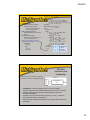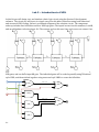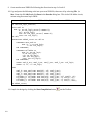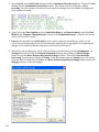
1
Sponsored by National Science Foundation Advanced Technological Education Award No. DUE-1003389 VHDL and FPGA Design Workshop Nasser Alaraje, PhD Michigan Tech University Associate Professor, Program Chair, Electrical Engineering Technology E-mail: [email protected] Aleksandr Sergeyev, PhD Michigan Tech University Assistant Professor, Electrical Engineering Technology E-mail: [email protected] Fred Scheu College of Lake County Instructor, Program Chair, Electrical Engineering Technology E-mail: [email protected] Carl Seidel EET Student, Senior Michigan Tech University E-mail: [email protected] 8/29/2011 Sponsored by National Science Foundation Advanced Technological Education Award No. DUE-1003389 VHDL and FPGA Design Workshop Nasser Alaraje, PhD Michigan Tech University Associate Professor, Program Chair, Electrical Engineering Technology E-mail: [email protected] Aleksandr Sergeyev, PhD Michigan Tech University Assistant Professor, Electrical Engineering Technology E-mail: [email protected] Fred Scheu College of Lake County Instructor, Program Chair, Electrical Engineering Technology E-mail: [email protected] Carl Seidel EET Student, Senior Michigan Tech University E-mail: [email protected] Syllabus y y y y y y y y y y y y y Day 1 9:00 am 9:15 am 9:45 am 1:00 pm 2:30 pm 3:30 am Day 2 9:00 am 10:00 am 11:00 am 1:00 pm 3:00 pm 3:30 pm 4:00 pm Introduction What is an FPGA FPGA Design Techniques Lab 1 – Introduction to Altera’s Quartus Introduction to VHDL Lab 2 - Introduction to VHDL Lab 3 - VHDL Testbench Lab Advanced VHDL Lab 4 – Advanced VHDL Final Project (using DE2) Support System (Software/hardware) Implementation / Adaption Plan / Issues at schools Conclusions / Feedback / Survey 1 8/29/2011 Introductions • Your Name Your Name • Your Affiliations • Experience with VHDL and FPGA gg • Your intended learning goals • Pre‐test / Pre‐Survey Workshop Goals: • Participants will: • Be able to identify the importance of teaching engineering technology students relevant skills in hardware modeling and FPGA design • Demonstrate the understanding of the fundamental concepts of hardware description languages and gain knowledge on programmable logic devices (PLD) • Gain hands‐on expertise on the hardware and software necessary to establish a re configurable lab at their necessary to establish a re‐configurable lab at their respective institutions • Gain hands‐on lab experience by practicing modeling basic building blocks of digital systems and learn the FPGA design flow • Develop potential curricular resources to be used at their respective institutions 2 8/29/2011 Introduction • FPGA‐based re‐programmable logic design became more G based e p og a ab e og c des g beca e o e attractive as a design medium during the last decade • only 19.5 % of 4‐year and 16.5 % of 2‐year electrical and computer engineering technology programs at US academic institutions currently have a curriculum component in hardware description language and programmable logic design • Curriculum has not yet “caught up” to industry needs. industry must be driving the curriculum development. 5 Research Background • Respond to the Market needs of Skilled FPGA Engineers • Historically, electrical engineering technology Associate Hi t i ll l t i l i i t h l A i t and Baccalaureate programs have included a traditional logic design course. These topics are far from most current industry practice in logic design. • EET two‐year and four‐year programs must teach digital logic using VHDL and FPGA [3] and students must be equipped with design skills that are current relevant and equipped with design skills that are current, relevant, and widely used in industry • The major objectives of this curriculum shift are to give technology students at Michigan Technological and College of Lake County the opportunity to learn and experience logic design using FPGA 6 3 8/29/2011 FPGA • Introduced by Xilinx in mid 1980 for implementing digital logic F ield P rogrammable G ate A rray • FPGA Can be visualized as a set of programmable logic blocks embedded in programmable interconnect • Interconnect architecture provides the connectivity between logic blocks • Programming Technology determines the method of storing configuration 7 FPGA Re‐programmable Logic Applications • When FPGA first introduced, it was considered as another form of gate array • SRAM‐FPGA in‐circuit reprogrammability feature provides a more than just a standard gate array • FPGAs have gained rapid acceptance and growth over the past decade because they can be applied to a very wide range of applications – random logic – Custom computing machine Custom computing machine – device controllers – communication encoding and filtering • programmable logic becomes the dominant form of digital logic design and implementation 8 4 8/29/2011 FPGA design flow • Design Flow is the step‐by‐step methodology to go through the process of FPGA design • The design flow can be divided into 6 basic steps Design Entry Functional Verification and Simulation FPGA S h i FPGA Synthesis FPGA Place & Route Circuit Analysis (Timing, Power …) Programming FPGA devices 9 FPGA Design Flow Implementation Path Analysis Path FUNCTIONAL VERIFICATION design entry (VHDL) & SIMULATION CIRCUIT ANALYSIS FPGA Synthesis (Timing) FPGA Place and Route Download to FPGA 10 5 8/29/2011 Description of Design steps • Design Entry – describes the design that has to be implemented onto FPGA • Functional Verification and Simulation – checks logical correctness of design • FPGA synthesis – converts design entry into actual gates/blocks needed • FPGA Place & Route – FPGA Place & Route selects the optimal position and selects the optimal position and minimizes length of interconnections on device • Time Analysis – determines the speed of the circuit which has been completely placed and routed • Programming to FPGA – downloads bitstream codes onto FPGA devices 11 Cyclone II FPGA Architecture The Cyclone II FPGA has up to: • 68,416 logic elements in the logic arrays. • 150 18x18‐bit embedded multipliers. multipliers • 250 M4K RAM blocks • 622 I/O element pins • Four phased‐locked loops 6 8/29/2011 What projects are FPGAs good for y y y y y y y y Aerospace & Defense Radiation‐tolerant Radiation tolerant FPGAs along with intellectual property for image processing, waveform generation, and partial FPGAs along with intellectual property for image processing waveform generation and partial reconfiguration for SDRs. Automotive Automotive silicon and IP solutions for gateway and driver assistance systems, comfort, convenience, and in‐vehicle infotainment. Broadcast Solutions enabling a vast array of broadcast chain tasks as video and audio finds its way from the studio to production and transmission and then to the consumer. Consumer Cost‐effective solutions enabling next generation, full‐featured consumer applications, such as converged handsets, digital flat panel displays, information appliances, home networking, and residential set top boxes. Industrial/Scientific/Medical Industry‐compliant solutions addressing market‐specific needs and challenges in industrial automation, motor control, and high‐end high end medical imaging. medical imaging Storage & Server Data processing solutions for Network Attached Storage (NAS), Storage Area Network (SAN), servers, storage appliances, and more. Wireless Communications RF, base band, connectivity, transport and networking solutions for wireless equipment, addressing standards such as WCDMA, HSDPA, WiMAX and others. Wired Communications End‐to‐end solutions for the Reprogrammable Networking Linecard Packet Processing, Framer/MAC, serial backplanes, and more www.fpgajobs.com pg j Who uses them 7 8/29/2011 • FPGA’s are horrendously complex (much more than computer software) – – – – Why Help is Needed Many tools, coding systems, etc. Analog (non‐ideal) timing behavior Many types of devices Code synthesis/Place & Route are not deterministic • In short a design frequently s o t a des g eque t y – Is theoretically correct – Simulates OK – Fails in a real part Why are they important • They have the ability to revolutionize the way that prototyping is done. • Allows companies to get to market quicker and stay in market longer stay in market longer. 8 8/29/2011 Xilinx • • • • Largest manufacturer of HW Develop hardware and software Embedded PowerPC University Program Altera • Second largest manufacturer • Develop HW and SW • University Program 9 8/29/2011 Which is best? Which is best? • It depends – Time – Existing resources – Money Money – Level of effort – Preference University Programs • Major manufacturers want to provide you with the resources to be successful 10 8/29/2011 • • • • AUP Altera University Program SBROWN@altera com (Stephen Brown) [email protected] (Stephen Brown) Very aggressive at supporting schools Pros – Good software and hardware • Cons – have limited educational support material XUP • Xilinx University Program • [email protected] xup@xilinx com • Only give away what they make or have signicant investment in • Pros – Give away hardware and software Give away hardware and software • Cons – Slow and not a positive donation 11 8/29/2011 Altera DE2 Development Board What do you really need to start? y y • Quartus Software • DE2 FPGA board 12 8/29/2011 Obtaining, licensing and service contract with Altera contract with Altera • If you decide to go with Altera, we can help you (with currently available resources) – Register with AUP – Get software Quartus Software • Quratus is the software used to make the project we are going to complete. • We will cover this package more in the next slides and during the practical exercise. 13 8/29/2011 Quartus® II Software Design Series: Foundation Objectives • • • • • • • Create a new Quartus® II project Choose supported design entry methods Compile a design into an FPGA Locate resulting compilation information Create design constraints (assignments & settings) Manage I/O assignments Manage I/O assignments Perform timing analysis & obtain results 28 14 8/29/2011 A Complete Solutions Portfolio CPLDs Low-cost FPGAs Embedded soft processors High-density, high-performance FPGAs Intellectual Property (IP) Design software Mid-range Transceiver FPGAs ASICs Development kits 29 Quartus II Software – Two Editions Subscription Edition Web Edition Devices Supported All Selected Devices Features 100% 95% Distribution Internet & DVD Internet & DVD Price Paid Free (no license required) Feature Comparison available on Altera web site 30 15 8/29/2011 Quartus II Design Software • Fully‐integrated development tool – Multiple design entry methods – Logic synthesis – Place & route – Timing & power analysis – Simulation (ModelSim‐Altera Edition) – Device programming 31 More Features • • • • • • • • • MegaWizard® Plug Plug‐In In Manager & SOPC Builder design tools Manager & SOPC Builder design tools TimeQuest Timing Analyzer Incremental compilation feature PowerPlay Power Analyzer NativeLink® 3rd‐party EDA tool integration Debugging capabilities ‐ From HDL to device in‐system 32 & 64‐bit Windows & Linux support Multi‐processor support Node‐locked & network licensing options 32 16 8/29/2011 Welcome to the Quartus II Software! Turn on or off in Tools ⇒ Options 33 Quartus II Default Operating Environment Project Navigator Tool View window Tasks window Messages window 34 17 8/29/2011 Dynamic menus File control Compilation controls Pin Planner Chip Planner Compilation Report TimeQuest timing analyzer Main Toolbar To reset views: 1. Tools ⇒ Customize ⇒ Toolbars ⇒ Reset All 2. Restart Quartus II 35 Tips & Tricks Advisor Help menu ⇒ Tips & Tricks Provides useful instructions on using sing the Quartus Q art s II soft software are & links to settings. Available sections include: • New features in current release • Helpful features and project settings available to designers 36 18 8/29/2011 Shortcut to Altera forums Expand all topics Web browser-based allows for easy search in page 37 Built‐In Help System Help menu ⇒ Getting Started Tutorial or from the Getting Started window 38 Interactive Tutorial 19 8/29/2011 Detachable Windows Click again to re-attach Click to detach window • Separate child windows from the Quartus II GUI frame (Window menu ⇒ Detach/Attach Window) 39 Tasks Window • Easy access to most Quartus II functions • Organized into related tasks within three task flows Organized into related tasks within three task flows Full Design Flow Perform all project tasks Compilation Flow Focus on compilation tasks Early Timing Estimate Faster compile iterations 40 Double-click any task to run 20 8/29/2011 • Customize the Tasks display • Add Tcl scripts for quick access 41 Custom Task Flow Tcl Console Window • Enter and execute Tcl commands directly in the GUI View menu ⇒ Utility Windows ⇒ Tcl Console • Execute from command‐line using Tcl shell – quartus_sh –shell • Run complete scripts from Tools menu ⇒ Tcl Scripts 42 21 8/29/2011 Design Specification Typical PLD Design Flow Design entry/RTL coding - Behavioral or structural description of design RTL simulation - Functional simulation - Verify logic model & data flow LE M4K/M9K M512 I/O Synthesis (Mapping) - Translate design into device specific primitives - Optimization to meet required area & performance constraints - Quartus II synthesis y or 3rd p party y synthesis y tools - Result: Post-synthesis netlist Place & route (Fitting) - Map primitives to specific locations inside Target technology with reference to area & performance constraints - Specify routing resources to be used - Quartus II Fitter - Result: Post-fit netlist 43 Typical PLD Design Flow tclk Timing analysis (TimeQuest Timing Analyzer) - Verify y performance p specifications p were met - Static timing analysis Gate level simulation (optional) - Simulation with timing delays taken into account - Verify design will work in target technology PC board simulation & test - Simulate board design - Program & test device on board - Use SignalTap® II Logic Analyzer or other on-chip tools for debugging 44 22 8/29/2011 Quartus II Projects • Description – Collection of related design files & libraries – Must have a designated top‐level entity – Target a single device – Store settings in Quartus II Settings File (.QSF) – Compiled netlist Compiled netlist information stored in db folder in information stored in db folder in project directory • Create new projects with New Project Wizard 45 – Can be created using Tcl scripts New Project Wizard File menu Tasks Select working directory Name of project can be any name; recommend using top-level file name Top-level entity does not need to be the same name as top-level file name 46 Tcl: project_new <project_name> 23 8/29/2011 Add design files − Graphic − VHDL − Verilog − SystemVerilog − EDIF − VQM Add library paths − User libraries − MegaCore®/AMPPSM − Pre-compiled VHDL packages Tcl: set_global_assignment –name VHDL_FILE <filename.vhd> Tcl: set_global_assignment –name USER_LIBRARIES <library_path_name> Add Files 47 Device Selection Choose device family Filter results Let Fitter select part or Show advanced devices Choose specific part from list 48 Show advanced devices Tcl: set_global_assignment –name FAMILY “device family name” Tcl: set_global_assignment –name DEVICE <part_number> 24 8/29/2011 EDA Tool Settings Choose EDA tools and file formats Settings can be changed or added later See handbook for Tcl command format 49 Done! Review results & click Finish 50 25 8/29/2011 Top-Level file • Quartus II design entry Top-level design files can be schematic, HDL, or 3rd-Party netlist file – Text editor • VHDL • Verilog or SystemVerilog – Schematic editor .bdf .bsf .vhd Block Symbol Text file file file • Block Diagram File .v or .sv .v or .vhd Text file State Machine file – State machine editor • HDL from state machine file Generated within Quartus II software – Memory editor • HEX • MIF • 3rd‐party EDA tools – EDIF 2 0 0 – Verilog Quartus Mapping (.VQM) .edf .edif .v, vlg, .vhd, .vhdl, .vqm Text file Text file Imported from 3rd Party EDA tools Design Entry Methods • Mixing & matching design files allowed 51 Tasks window File ⇒ New or 52 in Toolbar Creating New Design Files (& Others) 26 8/29/2011 Text Design Entry • Quartus II Text Editor features – – – – – – – – – Block commenting Block commenting Line numbering in HDL text files Bookmarks Syntax coloring Find/replace text Find and highlight matching delimiters Function collapse/expand Create & edit sdc files for TimeQuest Create & edit .sdc files for TimeQuest timing analyzer (described later) timing analyzer (described later) Preview/editing of full design and construct HDL templates • Enter text description – VHDL (.vhd, .vhdl) – Verilog (.v, .vlg, .Verilog, .vh) – SystemVerilog (.sv) 53 Verilog & VHDL • VHDL ‐ VHSIC hardware description language – IEEE Std 1076 (1987 & 1993) supported IEEE Std 1076 (1987 & 1993) supported – Partial IEEE Std 1076‐2008 support – IEEE Std 1076.3 (1997) synthesis packages supported • Verilog – IEEE Std 1364 (1995 & 2001) & 1800 (SystemVerilog) supported • Use Quartus II integrated synthesis to synthesize • View supported commands in built‐in help 54 27 8/29/2011 Text Editor Features Find/highlight matching delimiters Bookmarks (on/off/jump to) Insert Template (Edit menu) Preview window: edit before inserting & save as user template Collapse/expand functions 55 Design Files Quartus II Full Compilation Flow Analysis & Elaboration Constraints & settings Synthesis Constraints & settings Fitter Executed in parallel (multi-processor or multicore systems only) Functional Simulation Functional Netlist Assembler TimeQuest Timing Analysis Programming & Configuration files Gate-Level EDA Netlist Writer 56 Simulation Post-Fit Simulation Files 28 8/29/2011 Start Compilation (Full) Start Analysis & Elaboration − − Checks syntax & builds hierarchy Performs initial synthesis Start Analysis & Synthesis Start Fitter − − − Synthesizes & optimizes code Places & routes design Generates output netlists Start Assembler Analyzers − − Generate programming files I/O Assignment − PowerPlay − SSN (Switching Noise) Start Design Assistant 57 • Default “flat” compilation flow Processing Options Compilation Design Flows – Design compiled as a whole Design compiled as a whole – Global optimizations performed • Incremental flow (on by default for new projects) – User assigns design partitions – Each partition processed separately; results merged – Post Post‐synthesis synthesis or post or post‐fit fit netlists netlists for partitions are for partitions are reused – Benefits 58 • Decrease compilation time • Preserve compilation results and timing performance • Enable faster timing closure 29 8/29/2011 View menu ⇒ Utility Windows Status bars indicate compilation progress Message window displays informational, warning, & error messages 59 Manually flag selected messages for later review Status & Message Windows Compilation Report Window ⇒ Detach Window to release from Quartus II workspace Each compiler executable generates separate folder 60 30 8/29/2011 Netlist Viewers • RTL Viewer – Schematic of design after Analysis and Elaboration S h i fd i f A l i d El b i – Visually check initial HDL before synthesis optimizations – Locate synthesized nodes for assigning constraints – Debug verification issues • Technology Map Viewers (Post‐Mapping or Post‐Fitting) – Graphically represents results of mapping (post‐synthesis) & fitting – Analyze critical timing paths graphically – Locate nodes & node names after optimizations (cross‐probing) 61 RTL Viewer Tools menu ⇒ Netlist Viewers or Tasks window “Compile Compile Design Design” tasks Find in hierarchy Schematic view 62 Hierarchy list Note: Must perform elaboration first (e.g. Analysis & Elaboration OR Analysis & Synthesis) 31 8/29/2011 • Schematic View (RTL Viewer) Represents design using logic blocks & nets – – – – – I/O pins p Registers Muxes Gates (AND, OR, etc.) Operators (adders, multipliers, etc.) Place pointer over any element in schematic to see details • Name • Internal resource count 63 Compilation Summary • Compilation includes synthesis & fitting • Compilation Report contains detailed information on compilation results • Use Quartus II software tools to understand how design was processed – – – – – RTL Viewer RTL Viewer Technology Map Viewers State Machine Viewer Chip Planner Resource Property Editors 64 32 8/29/2011 Synthesis & Fitting Control • Controlled using two methods – Settings Settings ‐ Project Project‐wide wide switches switches – Assignments ‐ Individual entity/node controls • Both accessed in Assignments menu or Tasks window • Stored in QSF file for project/revision 65 Settings • Project‐wide switches that affect entire design • Examples – Device selection – Synthesis optimization – Fitter settings – Physical synthesis – Design Assistant g • Located in Settings dialog box – Assignments menu – Set Project and Compiler Settings task in Tasks window 66 33 8/29/2011 Device Settings Dialog Box 67 Change settings • Top-level entity • Add/remove files • Libraries • Compiler settings • EDA tool settings • Synthesis settings • Fitter settings • Timing Analysis settings • Power analysis settings • SSN Analyzer settings Settings Dialog Box Tcl: set_global_assignment –name <assignment_name*> <value> 68 34 8/29/2011 Compilation Process Setting Examples • Smart compilation − Skips entire compiler modules when not required − Saves compiler time − Uses more disk space • Generate version-compatible database 69 Tcl: set_global_assignment -name SMART_RECOMPILE ON Physical Synthesis • Optimize during synthesis or re‐ synthesize based on Fitter output – Makes incremental changes that improve results for a given placement – Compensates for routing delays from Fitter – Apply globally (Settings) or only to specific design entities (Assignment Editor) 70 35 8/29/2011 Fitter Settings – Fitter Effort Standard Fit – Highest effort – Longest compile time Fast Fit – Faster compile – Possibly lesser performance Auto Fit – Compile stops after meeting timing – Conserves CPU time – Will mimic standard fit for hardto-fit designs – Default for new designs One fitting attempt 71 Tcl: set_global_assignment –name FITTER_EFFORT “<Effort Level>” I/O Planning Need • I/O standards increasing in complexity • FPGA/CPLD I/O structure increasing in complexity – Results in increased pin placement guidelines • PCB development performed simultaneously with FPGA design • Pin assignments need to be verified earlier in design cycle • Designers need easy way to transfer pin assignments into board tools 72 36 8/29/2011 Creating I/O‐Related Assignments • Pin Planner • Import from spreadsheet in CSV format • Type directly into QSF file • Scripting • Using synthesis attributes in HDL Note: Other methods/tools are available in the Quartus II software to make I/O assignments. The above are the most common or recommended. 73 Pin Planner • Interactive graphical tool for assigning pins – Drag & drop pin assignments – Set pin I/O standards – Reserve future I/O locations • Three main sections Three main sections Assignments menu ⇒ Pin Planner or “Assign Constraints” folder in Tasks window – Package View – All Pins list – Groups list 74 37 8/29/2011 Pin Planner Window (1) Package View ((Top p or Bottom)) Toolbar Groups list All Pins list 75 Pin Planner Window (2) • Package View – Displays graphical representation of chip package – Use to make or edit design I/O assignments – Use to locate other package pins (power & configuration pins) • All Pins list – Displays I/O pins (signals) in design as indicated by filter – Use to edit pin settings/properties directly d / d l • Groups list – Similar to All Pins list except displays only groups & buses – Use to make bus and group assignments – Use to create new user‐defined groups 76 38 8/29/2011 Assigning Pin Locations Using Pin Planner Drag & drop multiple highlighted pins or buses Drag & & drop drop single single pin; pin; Drag tooltips provide provide pin pin tooltips information information 77 Choose one-by-one or pin alignment direction (Pin Planner toolbar or Edit menu) Assigning Pin Locations Using Pin Planner (2) Double-click pin or I/O bank to open Properties dialog box 78 Drag & drop to I/O bank, VREF block bank block, or device edge Filter nodes displayed 39 8/29/2011 Assigning Pin Locations Using Pin Planner (3) • Select available locations from list of pins color‐coded by I/O bank 79 Show Fitter Placements • View I/O locations automatically selected by Fitter View ⇒ Show or in Toolbar 80 40 8/29/2011 Back‐ Annotation Green/brown pattern tt iindicates di t back-annotation Assignments menu 81 Verifying I/O Assignments 82 • I/O Assignment Analysis – Checks legality of all I/O assignments without full compilation without full compilation • Minimal requirements for running – I/O declaration • HDL port declaration Processing menu ⇒ Start ⇒ Start I/O • Reserved pin Assignment Analysis or Tasks window – Pin‐related assignments g • I/O standard Run from Pin Planner • Current strength toolbar • Pin location (pin, bank, edge) • PCI clamping diode • Toggle rate 41 8/29/2011 I/O Rules Checked • No internal logic – Checks I/O locations & constraints with respect to other I/O & I/O banks – Each I/O bank supports a single VCCIO • I/O connected to logic g – Checks I/O locations & constraints with respect to other I/O, I/O banks, & internal resources – PLL must be driven by a dedicated clock input pin Note: When working with design files, synthesize design before running I/O Assignment Analysis 83 I/O Assignment Analysis Output Compilation Report (Fitter section) • Pin-out file • I/O pin tables • Output pin loading • I/O rules checking* Messages on I/O assignment issues • Compiler assumptions • Device & pin migration issues • I/O bank voltages & standards 84 *Note: See Appendix for special reports and information generated only for Stratix II, Cyclone III, and newer devices 42 8/29/2011 Please go to Lab1 – Introduction to Altera’s Quartus in the Manual 85 Introduction to VHDL • Implement basic constructs of VHDL • Implement modeling structures of VHDL 86 43 8/29/2011 VHSIC (Very High Speed Integrated Circuit) Hardware VHDL Description Language 87 What is VHDL? • IEEE industry standard hardware description language • High‐level description language for both simulation & synthesis simulation & synthesis – Facilitates portability and productivity as design logic and verification stimulus are both vendor and tool independent 88 44 8/29/2011 Terminology • HDL – A hardware description language is a a d a e desc pt o a guage s a software programming language that is used to model a piece of hardware • Behavioral modeling ‐ A component is described by its input/output response described by its input/output response • Structural modeling ‐ A component is described by interconnecting lower‐level components/ primitives 89 Terminology (cont.) • Register Transfer Level (RTL) ‐ A type of behavioral modeling, for the purpose of synthesis – Hardware is implied or inferred – Synthesizable • Synthesis Synthesis ‐ Translating HDL to a circuit and Translating HDL to a circuit and then optimizing the represented circuit • Process – Basic unit of execution in VHDL – Process executions are converted to equivalent hardware 45 1,000 100 1960s/1970s: 10‐1,000 1980s: 1,000‐100,000 1990s: Millions 2000s: Billions Off b • 1970s – Documentation was hundreds of pages for large ICs • Imprecise – Need for better documentation 2018 2 2015 2 2012 2 x=1 x=1 On1 On2 On3 schematics "The system has four states. When in state Off, the system t outputs t t 0 andd stays t in state Off until the input becomes 1. In that case, the system enters state On1, followed by On2, and then On3, in which the system outputs 1. The system then returns to state Off." • 1980s b’ x=1 Combinational Logic b x b Combinational n1 logic n0 s1 s0 FSM outputs – IC behavior documented using combination of schematics, diagrams, and natural language ( (e.g., English) l h) 2009 2 Inputs: b; Outputs: x x=0 diagrams natural language 2006 2 2003 2 10 FSM inputs – – – – 10,000 1997 • Typical digital components per IC 100,000 2000 2 Digital Systems and HDLs Transistors per IC (millions) 8/29/2011 x n1 State register clk n0 s1 clk s0 State register 91 • Hardware description languages (HDLs) – Machine‐readable textual l languages for describing hardware f d ibi h d HDLs for Simulation ... CombLogic: PROCESS (Currstate, b) BEGIN CASE Currstate IS WHEN S_Off => x <= '0'; IF (b = '0') THEN Nextstate <= S_Off; ELSE Nextstate <= S_On1; END IF; WHEN S_On1 => x <= '1'; Nextstate <= S_On2; Clk_s WHEN S_On2 => x <= '1'; Rst_s Nextstate <= S_On3; Simulation b_s WHEN S_On3 => x <= '1'; 1 ; x_s Nextstate <= S_Off; END CASE; 10 20 30 40 50 60 70 8090100110 END PROCESS; ... – Schematic + documentation in one – HDL description became the precise, concise IC documentation – Simulator is a tool that automatically generates outputs values of a hardware module for a given sequence of input values. – VHDL originally defined for simulation of ICs • First, IC was designed • Then, IC was described in HDL for documentation 92 46 8/29/2011 VHDL • • VHDL: VHSIC Hardware Description Language – VHSIC: Very High Speed Integrated Circuit • Project of the U.S. Dept. of Defense – VHDL defined in 1980s – Syntax: like Ada software programming language • Ada also a U.S. DoD creation – IEEE adopted VHDL standard ("1076") in 1987 Other HDLs – Verilog: Defined in 1980s / C‐like syntax / IEEE standard ("1364") in 1995 • VHDL & Verilog very similar in capabilities, differ mostly in syntax – SystemC: Defined in 2000s by several companies / C++ libraries and macro routines / IEEE standard ("1666") in 2005 • Excels for system‐level; cumbersome for logic level ARCHITECTURE Beh OF DoorOpener IS BEGIN PROCESS(c, h, p) BGEIN f <= NOT(c) AND (h OR p); END PROCESS; END Beh; module DoorOpener(c,h,p,f); input c, h, p; output f; reg f; always @(c or h or p) begin f <= (~c) & (h | p); end endmodule #include "systemc.h" SC_MODULE(DoorOpener) { sc_in<sc_logic> c, h, p; sc out<sc logic> g f; ; SC_CTOR(DoorOpener) { SC_METHOD(comblogic); sensitive << c << h << p; } void comblogic() { f.write((~c.read()) & (h.read() | p. read())); } }; 93 VHDL Versions Version Comments VHDL 1987 Initial version accepted by IEEE VHDL 1993 First major update to language; Increased flexibility and added “missing” constructs & operations VHDL 2000 Minor update to language VHDL 2002 Minor update to language VHDL-2008* Second major update to language; Check tool for support * Course will cover constructs supported by the Quartus II software version 9.1. 94 47 8/29/2011 HDL • HDLs became increasingly used for designing ICs using top‐down design process – Design: Converting a higher‐level description Design: Converting a higher level description into a lower‐level one – Describe circuit in HDL, simulate • Physical design tools automatically convert to low‐level IC design – Describe behavior in HDL, simulate • e.g., Describe addition as A = B + C, rather than as circuit of hundreds of logic gates – Compact description, designers get function right first • Design circuit – Manually, or – Using synthesis tools, which automatically convert HDL behavior to HDL circuit – Simulate circuit, should match HDLs for Design and Synthesis HDL Clk_s Rst_s HDL behavior b_s x_s Synthesis 10 20 30 40 50 60 70 8090100110 Clk_s HDL circuit Rst_s b s b_s x_s Physical design 10 20 30 40 50 60 70 8090100110 95 • • • Use of HDLs for synthesis is growing – Circuits are more complex – Synthesis tools are maturing Synthesis tools are maturing But HDLs originally defined for simulation – General language – Many constructs not suitable for synthesis • e.g., "wait" statements, pointers, recursive function calls – Behavior description may simulate, but not synthesize, or may synthesize to y , y y incorrect or inefficient circuit Not necessarily synthesis tool's fault! HDLs for Synthesis Clk_s Simulate Rst_s HDL behavior b_s x_s Synthesis 10 20 30 40 50 60 70 8090100110 HDL circuit 96 48 8/29/2011 • HDL language – General and complex; many uses p ; y – But use for synthesizing circuits is greatly restricted • Synthesis tool understands: sensitivity lists, if statements, ... • Synthesis tool may not understand: wait statements, while loops, ..., even if the HDL simulates correctly – If the circuit is bad, don't blame If th i it i b d d 't bl the synthesis tool! – We will emphasize use of VHDL for design and synthesis HDLs for Synthesis Clk_s Simulate Rst_s HDL behavior b_s x_s 10 20 30 40 50 60 70 8090100110 Synthesis HDL circuit 97 Only the functionality of the circuit, no structure No specific hardware intent input1, .., inputn output1, .., outputn IF shift_left THEN FOR j IN high DOWNTO low LOOP shft(j) := shft(j-1); END LOOP; output1 <= shft AFTER 5ns; Left bit shifter 98 Behavioral Modeling 49 8/29/2011 Functionality and structure of the circuit Call out the specific hardware Higher-level component input1 output1 Lower-level Component1 Lower-level Component0 outputn inputn Structural Modeling 99 • Two sets of constructs: VHDL Basics – Simulation – Synthesis & simulation • • • • • The VHDL language is made up of reserved keywords The language is, for the most part, not CASE sensitive VHDL statements are terminated with a ; VHDL is white space insensitive VHDL is white space insensitive Comment support – ‐‐ : End of line (EOL) comment; everything from symbol to EOL is commented – /* */ : Delimited comment; everything between symbols is commented • Supported in VHDL‐2008 only 100 50 8/29/2011 VHDL Design Units • ENTITY – used to define external view of a model. i.e. symbol • ARCHITECTURE – used to define the function of the model. i.e. schematic • PACKAGE – Collection of information that can be referenced by VHDL models i e LIBRARY models. i.e. LIBRARY – Consists of two parts: PACKAGE declaration and PACKAGE body 101 ENTITY Declaration ENTITY <entity_name> IS Port Declarations END ENTITY <entity_name> ; (1076-1993 version) • Analogy : symbol – <entity_name> can be any alpha/numerical name • Port declarations – Used to describe the inputs and outputs i.e. pins • Generic declarations – Used to pass information into a model • Close entity in one of 3 ways – END ENTITY <entity_name>; -- VHDL ’93 and later – END ENTITY; -- VHDL ’93 and later – END; -- All VHDL versions 102 51 8/29/2011 ENTITY : Port Declarations ENTITY <entity_name> IS PORT ( SIGNAL clk : IN bit; --Note: SIGNAL is assumed and is not required q : OUT bit ); END ENTITY <entity_name> ; • Structure : <class> object_name : <mode> <type> ; • <class> : what can be done to an object • object_name : identifier (name) used to refer to object • <mode> : directional » IN (input) OUT (output) » INOUT (bidirectional) BUFFER (output w/ internal feedback) • <Type> : what can be contained in the object (discussed later) 103 • Analogy : schematic ARCHITECTURE – Describes the functionality and timing of a model • • • • Must be associated with an ENTITY ENTITY can have multiple architectures ARCHITECTURE statements execute concurrently (processes) ARCHITECTURE styles – Behavioral : how designs operate • RTL : designs are described in terms of registers • Functional : no timing – Structural : netlist • Gate/component level – Hybrid : mixture of the two styles • End architecture with – END ARCHITECTURE <architecture_name>; -- VHDL ’93 & later – END ARCHITECTURE; -- VHDL ’93 & later – END; -- All VHDL versions 104 52 8/29/2011 ARCHITECTURE ARCHITECTURE <identifier> OF <entity_identifier> IS --ARCHITECTURE declaration section (list does not include all) SIGNAL temp : INTEGER := 1; -- signal declarations with optional default values CONSTANT load : boolean := true; --constant declarations --Type declarations (discussed later) --Component declarations (discussed later) --Subprogram declarations (discussed later) --Subprogram body (discussed later) --Subtype declarations --Attribute declarations --Attribute specifications BEGIN PROCESS statements t t t Concurrent procedural calls Concurrent signal assignment Component instantiation statements Generate statements END ARCHITECTURE <architecture_identifier>; 105 VHDL ‐ Basic Modeling Structure ENTITY entity_name IS portt declarations d l ti END ENTITY entity_name; ARCHITECTURE arch_name OF entity_name IS internal signal declarations enumerated data type declarations component declarations d l BEGIN signal assignment statements PROCESS statements component instantiations 106 END ARCHITECTURE arch_name; 53 8/29/2011 ENTITY cmpl_sig IS PORT ( a, b, sel : IN BIT; x, y, z : OUT BIT ); END ENTITY cmpl_sig; ARCHITECTURE logic OF cmpl_sig IS BEGIN -- simple signal assignment x <= (a AND NOT sel) OR (b AND sel); -- conditional signal assignment y <= a WHEN sel='0' ELSE b; -- selected signal g assignment g WITH sel SELECT z <= a WHEN '0', b WHEN '1', '0' WHEN OTHERS; END ARCHITECTURE logic; Putting It All Together ENTITY ARCHITECTURE a a b x x sel a b b sel a b sel y z y z sel 107 Libraries • A LIBRARY is a directory that contains a package or a collection of packages • Two types of libraries – Working library • Current project directory – Resource libraries • • • • STANDARD package IEEE developed packages Altera component packages Any LIBRARY of design units that is referenced in a design 108 54 8/29/2011 Example LIBRARY IEEE; USE IEEE.STD_LOGIC_1164.ALL; ENTITY cmpl_sig l i IS PORT ( a, b, sel : IN STD_LOGIC; x, y, z : OUT STD_LOGIC); END ENTITY cmpl_sig; ARCHITECTURE logic OF cmpl_sig IS BEGIN -- Simple signal assignment X <= (a AND NOT sel) OR (b AND sel); -- Conditional signal assignment Y <= a WHEN sel='0' ELSE B; -- Selected signal assignment WITH sel SELECT Z <= a WHEN '0', B WHEN '1', '0' WHEN OTHERS; END ARCHITECTURE logic; • LIBRARY <name>, <name> ; – Name is symbolic and defined by y y compiler tool Ö Note: Remember that WORK and STD do not need to be defined. • USE lib_name.pack_name.object; – ALL is a reserved word for object name • Pl Placing the library/use clause first will i th lib / l fi t ill allow all following design units to access it 109 Types Defined in STANDARD Package • Type BIT – 2 logic value system (‘0’, ‘1’) g y ( ) SIGNAL a_temp : BIT; – Bit_vector array of bits SIGNAL temp : BIT_VECTOR (3 DOWNTO 0); SIGNAL temp : BIT_VECTOR (0 TO 3); • Type BOOLEAN – (False, true) • Type INTEGER – Positive and negative values in decimal SIGNAL int_tmp : INTEGER; -- 32-bit number SIGNAL int_tmp1 : INTEGER RANGE 0 TO 255; --8 bit number 110 55 8/29/2011 • Type NATURAL Other Types Defined in Standard Package 32 – Integer with range 0 to 2 g g • Type POSITIVE – Integer with range 1 to 232 • Type CHARACTER – ASCII characters • Type STRING – Array of characters Array of characters • Type TIME – Value includes units of time (e.g. ps, us, ns, ms, sec, min, hr) • Type REAL – Double‐precision floating point numbers Libraries (cont.) • LIBRARY IEEE – Contains the following packages • STD_LOGIC_1164 (STD_LOGIC types & related functions) • NUMERIC_STD (unsigned arithmetic functions using standard logic vectors defined as SIGNED and UNSIGNED data type) • STD_LOGIC_ARITH* (arithmetic functions using standard logic vectors as SIGNED or UNSIGNED) • STD_LOGIC_SIGNED* (signed arithmetic functions directly using standard logic vectors) • STD_LOGIC_UNSIGNED* (unsigned arithmetic functions directly using standard logic vectors) • STD_LOGIC_TEXTIO* (file operations using std_logic) * Packages actually developed by Synopsys but accepted and supported as standard VHDL by most synthesis and simulation tools 112 56 8/29/2011 Types Defined in STD_LOGIC_1164 Package • Type STD_LOGIC – 9 logic value system (‘U’, ‘X’, ‘0’, ‘1’, ‘Z’, ‘W’, ‘L’, ‘H’, ‘‐’) z ‘1’: Logic high z ‘U’: Undefined z ‘0’: Logic low z ‘H’: Weak logic high z ‘X: Unknown z ‘L’: Weak logic low z ‘Z’: (not ‘z’) Tri-state z ‘W’: Weak unknown z ‘-’: Don’t Care – Resolved type: supports signals with multiple drivers • Driving multiple values onto same signal results in known value Driving multiple values onto same signal results in known value • Type STD_ULOGIC – Same 9 value system as STD_LOGIC – Unresolved type: Does not support multiple signal drivers • Driving multiple values onto same signal results in error AND/OR/NOT Gates x y ENTITY And2 PORT (x: y: F: END And2; F IS IN std_logic; IN std_logic; OUT std_logic); x y F Entities and Ports x F ENTITY Or2 IS PORT (x: IN std_logic; y: IN std_logic; F: OUT std_logic); END Or2; ENTITY Inv IS PORT (x: IN std_logic; F: OUT std_logic); END Inv; • ENTITY – Declares a new type of component – Named “And2” in this example N d “A d2” i thi l • PORT( ); – List of inputs and outputs of entity – “x: IN std_logic” Æ port “x” is an input port of type std_logic • std_logic short for “standard logic,” a logical bit type (versus say an integer type), which can be '0' or '1' (more later) – Ports in list separated by semicolons “;” 114 57 8/29/2011 AND/OR/NOT Gates Entities and Ports x F y ENTITY And2 PORT (x: y: F: END And2; • • • IS IN std_logic; IN std_logic; OUT std_logic); x y x F ENTITY Or2 IS PORT (x: IN std_logic; y: IN std_logic; F: OUT std_logic); END Or2; F ENTITY Inv IS PORT (x: IN std_logic; F: OUT std_logic); END Inv; VHDL has several dozen reserved words – ENTITY, IS, PORT, IN, OUT, and END are reserved words above – Our convention: Reserved words are UPPER CASE – User cannot use reserved words when naming items like ports or entities User‐defined names – Begin with letter, optionally followed by sequence of letters, numbers, or underscore • No two underscores in a row, and can't end in underscore – Valid names: A, x, Hello, JXYZ, B14, Sig432, Wire_23, Index_counter_1, In1, test_entity – Invalid names: IN (reserved word), Wire_ (ends in underscore), Wire__23 (two underscores in a row), 4x1Mux (doesn’t start with a letter), _in4 (doesn’t start with a letter) Note: VHDL is case insensitive. ENTITY, Entity, entity, even EnTiTy, all mean the same 115 • • • • • • • • • Constants g Signals Signal Assignments Operators Processes Variables Sequential Statements Subprograms Types Architecture Modeling Fundamentals 116 58 8/29/2011 Constants • Associates value to name • Constant declaration – Can be declared in ENTITY, ARCHITECTURE or PACKAGE Can be declared in ENTITY ARCHITECTURE or PACKAGE CONSTANT <name> : <DATA_TYPE> := <value>; CONSTANT bus_width : INTEGER := 16; • Cannot be changed by executing code – Remember generics are constants (parameters) that can be overwritten by passing new values into the entity at compile time, not during code execution • Improves code readability • Increases code flexibility 117 Signals • Signals represent physical interconnect (wire) that communicate between processes (functions) PROCESS PROCESS Signals Functional Block Signals Functional Block Signals Signals • Signal declaration – Can be declared in PACKAGE, ENTITY and ARCHITECTURE SIGNAL temp : STD_LOGIC_VECTOR (7 DOWNTO 0); 118 59 8/29/2011 Assigning Values to Signals SIGNAL temp : STD_LOGIC_VECTOR (7 DOWNTO 0); • Signal assignments are represented by <= • Examples – All bits temp <= “10101010”; temp <= x”aa” ; (1076-1993) – VHDL also supports ‘o’ for octal and ‘b’ for binary – Bit‐slicingg temp (7 DOWNTO 4) <= “1010”; – Single bit temp(7) <= ‘1’; • Use double‐quotes (“ “) to assign multi‐bit values and single‐ quotes (‘ ‘) to assign single‐bit values 119 Simple Signal Assignments Format: <signal_name> <= <expression>; Example: qa <= r OR t ; qb <= (qa AND NOT (g XOR h)); r t g 2 implied processes Ö Parenthesis ( ) give the order of operation qb b h Expressions use VHDL operators to describe behavior 120 60 8/29/2011 Standard VHDL Operators Operator Type Operator Name/Symbol Logical NOT AND NAND NOR OR XOR Relational = <= Shifting(1)(2) SLL SRL SLA SRA ROL ROR Addition & Sign + Concatenation & Multiplication * Arithmetic Miscellaneous ** = exponentiation abs = absolute value ** /= < Priority XNOR(1) > Low >= - / MOD REM High ABS (1) Not supported in VHDL ’87 (2) Supported in NUMERIC_STD package for SIGNED/UNSIGNED data types 121 ENTITY opr IS PORT ( a : IN INTEGER RANGE 0 TO 16; 16 b : IN INTEGER RANGE 0 TO 16; sum : OUT INTEGER RANGE 0 TO 32 ); END ENTITY opr; ARCHITECTURE example OF opr IS BEGIN sum < <= a + b; END ARCHITECTURE example; Arithmetic Function The VHDL compiler can understand this operation because an arithmetic operation is defined for the built-in data type INTEGER Ö Note: remember the library STD and the package STANDARD do not need to be referenced 122 61 8/29/2011 Conditional Signal Assignments Format: <signal_name> <= <signal/value> WHEN <condition_1> ELSE <signal/value> WHEN <condition_2> ELSE … <signal/value> WHEN <condition_n> ELSE <signal/value>; Example: q <= a WHEN sela = ‘1’ ELSE b WHEN selb = ‘1’ ELSE c; 123 c b selb q a sela Implied process Selected Signal Assignments Format: WITH <expression> SELECT <signal_name> <= <signal/value> WHEN <condition_1>, <signal/value> WHEN <condition_2>, … <signal/value> WHEN OTHERS; Example: WITH sel SELECT q <= a WHEN “00”, b WHEN “01”,, c WHEN “10”, d WHEN OTHERS; a b c d sel q 2 Implied process 124 62 8/29/2011 Selected Signal Assignments • All possible conditions must be considered • WHEN OTHERS clause evaluates all other possible conditions that are not specifically stated See next slide 125 LIBRARY IEEE; USE IEEE.STD_LOGIC_1164.ALL; ENTITY cmpl_sig IS PORT ( a, b, sel : IN STD_LOGIC; z : OUT STD_LOGIC ); END ENTITY cmpl_sig; ARCHITECTURE logic OF cmpl_sig IS BEGIN -- Selected signal assignment WITH sel SELECT z <= a WHEN '0', b WHEN '1', '0' WHEN OTHERS; END ARCHITECTURE logic; Selected Signal Assignment sel is of STD_LOGIC STD LOGIC data type • What are the values for a STD_LOGIC data type • Answer: {‘0’,’1’,’X’,’Z’…} • Therefore, is the WHEN OTHERS clause necessary? • Answer: YES 126 63 8/29/2011 VHDL Model ‐ Concurrent Signal Assignments LIBRARY IEEE; USE IEEE.STD_LOGIC_1164.ALL; ENTITY cmpl_sig is PORT ( a, b, sel : IN STD_LOGIC; x, y, z : OUT STD_LOGIC ); END ENTITY cmpl_sig; • The signal assignments execute in parallel, and therefore the order we list the statements should not affect the outcome ENTITY ARCHITECTURE a b ARCHITECTURE logic OF cmpl_sig IS BEGIN -- Simple signal assignment x <= (a AND NOT sel) OR (b AND sel); -- Conditional signal assignment y <= a WHEN sel='0' ELSE b; -- Selected signal assignment WITH sel SELECT z <= a WHEN '0', b WHEN '1', ‘X' WHEN OTHERS; END ARCHITECTURE logic; a x x sel a b b sel a b sel y z y z sel 127 Process Statements • Implicit process – Types • Concurrent signal assignments • Component instantiations – Process sensitive to all inputs Process sensitive to all inputs • e.g. Read side of signal assignment • Explicit process – PROCESS keyword defines process boundary 128 64 8/29/2011 Explicit PROCESS Statement • Process sensitive to explicit (optional) sensitivity list – Events Events (transitions) on signals in (transitions) on signals in sensitivity list trigger process • 0→1, X→1, 1→Z, etc • Declaration section allows declaration of local objects and names • Process contents consist of sequential statements and sequential statements and simple signal assignments -- Explicit PROCESS statement label : PROCESS (sensitivity_list) Constant declarations d l i Type declarations Variable declarations BEGIN Sequential statement #1; … Sequential statement #n ; END PROCESS; 129 Execution of PROCESS Statement • Process statement is executed infinitely unless broken by a WAIT statement or sensitivity list • Sensitivity list implies a WAIT statement at the end of the process – Due to all processes being executed once at beginning of model execution • Process can have multiple WAIT statements • Process can not have both a sensitivity list and WAIT statement Ö Note: Logic synthesis places restrictions on the usage of WAIT statements as well as on the usage of sensitivity lists PROCESS (a,b) (a b) BEGIN Sequential statements END PROCESS; PROCESS BEGIN Sequential statements WAIT ON (a,b) ; END PROCESS; 130 65 8/29/2011 Multi‐Process Architectures A R C H I T E C T U R E PROCESS 1 Sequential Statement Signals Signals PROCESS N Sequential Statement Describes the functionality of design An architecture can have multiple process statements Each p process executes in parallel with other processes Order of process blocks does not matter Within a process, the statements are executed sequentially Order of statements within a process does matter 131 YES LIBRARY IEEE; USE IEEE.STD_LOGIC_1164.ALL; LIBRARY IEEE; USE IEEE.STD_LOGIC_1164.ALL; ENTITY simp IS PORT ( a, b : IN STD_LOGIC; y : OUT STD_LOGIC ); END ENTITY simp; ARCHITECTURE logic OF simp IS SIGNAL c : STD_LOGIC; BEGIN c <= a AND b; y <= c; END ARCHITECTURE logic; c AND y get executed and updated in parallel at the end of the process within one simulation cycle Equivalent Functions?? 9 ENTITY simp_prc IS PORT ( a,b : IN STD_LOGIC; y : OUT STD_LOGIC ); END ENTITY simp_prc; ARCHITECTURE logic OF simp_prc IS SIGNAL c : STD_LOGIC; BEGIN process1: PROCESS (a, b) BEGIN c <= a AND b; END PROCESS process1; process2: PROCESS (c) BEGIN y <= c; END PROCESS process2; END ARCHITECTURE logic; 132 66 8/29/2011 LIBRARY IEEE; USE IEEE.STD_LOGIC_1164.ALL; Equivalent Functions?? NO ENTITY simp IS PORT ( a, b : IN STD_LOGIC; y : OUT STD_LOGIC ); END ENTITY simp; ARCHITECTURE logic OF simp IS SIGNAL c : STD_LOGIC; BEGIN c <= a AND b; y <= c; END ARCHITECTURE logic; [ New value of c not available for y until next process execution (requires another simulation cycle or transition on a/b) LIBRARY IEEE; USE IEEE.STD_LOGIC_1164.ALL; ENTITY simp_prc IS PORT ( a, b : IN STD_LOGIC; y: OUT STD_LOGIC ); END ENTITY simp_prc; ARCHITECTURE logic OF simp_prc IS SIGNAL c: STD_LOGIC; BEGIN PROCESS (a, b) BEGIN c <= a AND b; y <= c; END PROCESS; END ARCHITECTURE logic; 133 IF‐THEN Statements Example: Format: IF <condition1> THEN {sequence of statement(s)} ELSIF <condition2> THEN {sequence of statement(s)} … ELSE {sequence of statement(s)} END IF; IF PROCESS (sela, (sela selb, selb a, a b, b c) BEGIN IF sela=‘1’ THEN q <= a; ELSIF selb=‘1’ THEN q <= b; ELSE q <= c; END IF; END PROCESS; c b selb a q sela 67 8/29/2011 Sequential Statements • Indicate behavior and express order • Must be used inside explicit processes • Sequential statements – – – – IF‐THEN statement CASE CASE statement Looping statements WAIT statements 135 IF‐THEN Statements • Similar to conditional signal assignment I Implicit li it Process P E li it Process Explicit P q <= a WHEN sela = ‘1’ ELSE b WHEN selb = ‘1’ ELSE c; c b selb a sela q PROCESS (sela, selb, a, b, c) BEGIN IF sela=‘1’ THEN q <= a; ELSIF selb=‘1’ THEN q <= b; ELSE q <= c; END IF; END PROCESS; 136 68 8/29/2011 CASE Statement Example: Format: CASE {expression} IS WHEN <condition1> => {sequence of statements} WHEN <condition2> => {sequence of statements} … WHEN OTHERS => -- (optional) {sequence of statements} END CASE; CASE a b c d sel PROCESS (sel, a, b, c, d) BEGIN CASE sel IS WHEN “00” => q <= a; WHEN “01” => q <= b; WHEN “10” => q <= c; WHEN OTHERS => q <= d; END CASE; END PROCESS; q 2 CASE Statement • Similar to selected signal assignment Implicit Process WITH sel SELECT q <= a WHEN “00”, b WHEN “01”, c WHEN “10”, d WHEN OTHERS; a b c d sel q 2 Explicit Process PROCESS (sel, a, b, c, d) BEGIN CASE sel IS WHEN “00” => q <= a; WHEN “01” => q <= b; WHEN “10” => q <= c; WHEN OTHERS => q <= d; END CASE; END PROCESS; 138 69 8/29/2011 Sequential LOOPS Infinite Loop • Infinite loop p – Loops forever • While loop – Loops until conditional test is false • For loop – Loops for certain number of Iterations – Note: Iteration identifier not required to be previously declared • Additional loop commands (each requires loop label) – NEXT / NEXT WHEN • Skips to next loop iteration – EXIT / EXIT WHEN • Cancels loop execution [Loop_label]: [Loop label]: LOOP --Sequential statement EXIT loop_label ; END LOOP; While Loop WHILE <condition> LOOP --Sequential statements END LOOP; For Loop FOR <identifier> IN <range> LOOP --Sequential statements END LOOP; 139 WAIT Statements Pauses execution of process until WAIT statement is satisfied • • Types – WAIT ON <signal> • Pauses until signal event occurs WAIT ON a, b; – WAIT UNTIL <boolean_expression> • Pauses until boolean expression is true WAIT UNTIL (int < 100); – WAIT FOR <time_expression> WAIT FOR <time expression> • Pauses until time specified by expression has elapsed WAIT FOR 20 ns; – Combined WAIT WAIT UNTIL (a = ‘1’) FOR 5 us; * Wait statement usage limited in synthesis 140 70 8/29/2011 Using WAIT Statements stim: PROCESS VARIABLE error : BOOLEAN; BEGIN WAIT UNTIL clk = ‘0’; a <= (OTHERS => ‘0’); b <= (OTHERS => ‘0’); WAIT FOR 40 NS; IF (sum /= 0) THEN error := TRUE; END IF; Pause execution of the process until clk transitions to a logic 0 Pause execution of the process until the equivalent of 40 ns passes in simulation time WAIT UNTIL clk = ‘0’; a <= “0010”; b <= “0011”; WAIT FOR 40 NS; IF (sum /= 5) THEN error := TRUE; END IF; … Pause execution of the process indefinitely WAIT; 141 END PROCESS stim; Two Types of RTL Process Statements • Combinatorial process – Sensitive to all inputs read by the process • Example PROCESS (a, b, sel) PROCESS (ALL) -- VHDL-2008 a c b sel Sensitivity list includes all inputs used by the combinatorial logic • Sequential process – Sensitive to select inputs (clock and asynchronous control signals) • Example PROCESS (clr, clk) 142 d D Q q clk ENA ACLR_N aclr_n Sensitivity list does not include the d input, only the clock or/and control signals 71 8/29/2011 DFF dff1 LIBRARY IEEE; USE IEEE.STD_LOGIC_1164.ALL; d ENTITY dff1 IS PORT ( d : IN STD_LOGIC; clk : IN STD_LOGIC; q : OUT STD_LOGIC ); END ENTITY dff1; ARCHITECTURE logic OF dff1 IS BEGIN PROCESS (clk) ( lk) BEGIN IF clk‘EVENT AND clk = '1' THEN q <= d; END IF; END PROCESS; END ARCHITECTURE behavior; D Q q clk ENA CLRN clk’EVENT AND clk=‘1’ – clk is the signal name (any name) – ’EVENT is a VHDL attribute, specifying that there needs To be a change in signal value – clk=‘1’ means positive-edge triggered 143 Types • VHDL has built‐in data types to model h d hardware (e.g. BIT, BOOLEAN, STD_LOGIC) ( BIT BOOLEAN STD LOGIC) • VHDL also allows creation of brand new types for declaring objects (i.e. constants, signals, variables) • Subtype • Enumerated Data Type • Array 144 72 8/29/2011 Subtype • A constrained type • Synthesizable if base type is synthesizable Synthesizable if base type is synthesizable • Use to make code more readable and flexible – Place in package to use throughout design ARCHITECTURE logic OF subtype_test IS SUBTYPE word IS std_logic_vector (31 DOWNTO 0); SIGNAL mem_read, mem_write : word; SUBTYPE dec_count IS INTEGER RANGE 0 TO 9; SIGNAL ones, tens : dec_count; BEGIN 145 • Enumerated Data Type Allows user to create data type name and values – Must create constant, signal or variable of that type to use • Used in U di – Making code more readable – Finite state machines • Enumerated type declaration TYPE <your_data_type> IS ((data type yp items or values separated p by y commas); ); TYPE enum IS (idle, fill, heat_w, wash, drain); SIGNAL dshwshr_st : enum; … drain_led <= ‘1’ WHEN dshwsher_st = drain ELSE ‘0’; 146 73 8/29/2011 Array • Creates multi‐dimensional data type for storing values – Must create constant, signal or variable of that type Must create constant signal or variable of that type • Used to create memories and store simulation vectors • Array type Declaration array depth TYPE <array_type_name> IS ARRAY (<integer_range>) OF <data_type>; yp what can be stored in each array address 147 Array Example ARCHITECTURE logic OF my_memory IS -- Creates new array data type named mem which has 64 -- address locations each 8 bits wide TYPE mem IS ARRAY (0 to 63) OF std_logic_vector (7 DOWNTO 0); -- Creates 2 - 64x8-bit array to use in design SIGNAL mem_64x8_a, mem_64x8_b : mem; BEGIN … mem_64x8_a(12) <= x“AF”; mem_64x8_b(50) <= “11110000”; … END ARCHITECTURE logic; 148 74 8/29/2011 Recall ‐ Structural Modeling • Functionality and structure of the circuit • Call out the specific hardware, lower‐level components Higher-level component Output1 Input1 Lower-Level Component2 Lower-Level Component1 149 Outputn Inputn Design Hierarchically ‐ Multiple Design Files • VHDL hierarchical design requires component declarations and component instantiations declarations and component instantiations Top.Vhd ENTITY-ARCHITECTURE “top” Component “mid_a” Component “mid_b” Mid_a.Vhd ENTITY-ARCHITECTURE “mid_a” Component “bottom_a” Bottom_a.Vhd ENTITY-ARCHITECTURE “bottom_a” Mid_b.Vhd ENTITY-ARCHITECTURE “mid_b” Component “bottom_a” Component “bottom_b” Bottom_b.Vhd ENTITY-ARCHITECTURE “bottom_b” 150 75 8/29/2011 Component Declaration and Instantiation • Component declaration ‐ used to declare the port types and the data types of the ports for a lower‐level design COMPONENT <lower-level_design_name> PORT ( <port_name> : <port_type> <data_type>; ... <Port_name> : <port_type> <data_type> ); END COMPONENT; • Component instantiation ‐ used to map the ports of a lower‐level design to that of the current‐level design <Instance_name> : <lower-level_design_name> PORT MAP(<lower-level_port_name> => <current_level_port_name>, …, <lower-level_port_name> => <current_level_port_name>); 151 • Hierarchical Circuits Using Entities as Components Entity can be used as component in a new entity • – AND AND entity used as component in entity used as component in CompCircuit entity – Can continue: CompCircuit entity can be used as component in another entity • And so on Hierarchy powerful mechanism for managing complexity CompCircuit CompCircuit3 CompCircuit2 x y CompCircuit F 152 76 8/29/2011 LIBRARY ieee; USE ieee.std_logic_1164.ALL; ENTITY Mux2 IS PORT (i1, i0: IN std_logic; s0: IN std_logic; d: OUT std_logic); END Mux2; • 4‐bit 2x1 mux example 2x1 mux circuit from earlier i0 i1 And2_1 n2 Or2_1 i0 n1 d n3 i1 Mux2 M 2 d s0 And2_2 Inv_1 Mux2 s0 ARCHITECTURE Struct OF Mux2 IS COMPONENT And2 IS PORT (x, y: IN std_logic; F: OUT std_logic); END COMPONENT; COMPONENT Or2 IS PORT (x, y: IN std_logic; F: OUT std_logic); END COMPONENT; COMPONENT Inv IS PORT (x: IN std_logic; F: OUT std_logic); END COMPONENT; SIGNAL n1, n2, n3: std_logic; BEGIN Inv_1: Inv And2_1: And2 And2_2: And2 Or2_1: Or2 END Struct; PORT PORT PORT PORT MAP MAP MAP MAP (s0, (i0, (i1, (n2, n1); n1, n2); s0, n3); n3, d); 153 • Multifunction Now consider register with control inputs, Register Behavior I3 such as load or shift – Could describe structurally • Four flip‐flops, four muxes, and some combinational logic (to convert control inputs to mux select inputs) I2 Shr Shl Operation 0 0 0 0 1 1 1 1 0 0 1 1 0 0 1 1 0 1 0 1 0 1 0 1 Maintain present value Shift left Shift right Shift right – Shr has priority over Shl Parallel load Parallel load – ld has priority Parallel load – ld has priority Parallel load – ld has priority I0 4-bit register g D D D Q D Q R clk Q R Q R R rst Q3 Q2 I3 Shr_in Ld Shr Shl – We'll describe behaviorally Ld I1 I2 Q1 I1 Q0 I0 Shl_in Rst Q3 Q2 Q1 Q0 ld shr shl Operation 0 0 0 1 0 0 1 X 0 1 X X Maintain value Shift left Shift right Parallel load Compact register operation table, 154 clearly showing priorities 77 8/29/2011 LIBRARY ieee; USE ieee.std_logic_1164.ALL; • Use IF statement – ELSIF parts ensure correct priority of control inputs • Rst has first priority, then Ld, then Shr, and finally Shl • Shift by assigning each bit – Recall that statement order doesn't matter • Use signal R for storage – Can't use port Q because OUT port cannot be read by process Use concurrent signal assignment to update Q when R changes – Equivalent to: process(R) begin Q <= R; end process; ARCHITECTURE Beh OF MfReg4 IS SIGNAL R R: std_logic_vector(3 td l i t (3 DOWNTO 0) 0); BEGIN PROCESS (Clk) BEGIN IF (Clk = '1' AND Clk'EVENT) THEN IF (Rst = '1') THEN R <= "0000"; ELSIF (Ld = '1') THEN R <= I; ELSIF (Shr = '1') THEN R(3) <= Shr_in; R(2) <= R(3); R(1) <= R(2); R(0) <= R(1); ELSIF ( (Shl = '1') ) THEN R(0) <= Shl_in; R(1) <= R(0); R(2) <= R(1); R(3) <= R(2); END IF; ld shr shl Operation END IF; END PROCESS; 0 0 0 Maintain value 0 0 1 Q <= R; END Beh; 0 1 X 1 X X Shift left Shift right Parallel load 155 AND Gate Simulation and Testbenches Idea: Create new "Testbench" entity that provides id test vectors to component's inputs i T tb h Testbench process • ENTITY MfReg4 IS PORT (I: IN std_logic_vector(3 DOWNTO 0); Q: OUT std_logic_vector(3 DOWNTO 0); Ld, Shr, Shl, Shr_in, Shl_in: IN std_logic; Clk, Rst: IN std_logic ); END MfReg4; x_s y_s x CompToTest y (And2) F F_s • A testbench is a setup for applying test vectors to test a design. • The setup creates an entity called Testbench having no inputs or outputs. • The setup instantiates a component representing the entity to be simulated, CompToTest • The setup uses a process that writes to signals x_s and y_s, which are connected to the inputs of CompToTest. • The process will contain statements that set the signals with the desired test vectors. 156 78 8/29/2011 LIBRARY ieee; USE ieee.std_logic_1164.ALL; ENTITY Testbench IS END Testbench; • HDL testbench – – – – Entity with no ports Entity with no ports Declare component to test Declare signal for each port Instantiate component, map signals to ports – Set signal values at desired times AND/OR/NOT Gates Simulation and Testbenches ARCHITECTURE TBarch OF Testbench IS COMPONENT And2 IS PORT (x: IN std_logic; y: IN std_logic; F: OUT std_logic); END COMPONENT; SIGNAL x_s, y_s, F_s: std_logic; BEGIN CompToTest: And2 PORT MAP (x_s, y_s, F_s); PROCESS BEGIN -- Test all y s <= y_s < '0'; 0 ; WAIT FOR 10 y_s <= '0'; WAIT FOR 10 y_s <= '1'; WAIT FOR 10 y_s <= '1'; WAIT; END PROCESS; END TBarch; possible input combinations x x_s s <= < '0'; 0 ; ns; x_s <= '1'; ns; x_s <= '0'; ns; x_s <= '1'; 157 LIBRARY ieee; USE ieee.std_logic_1164.ALL; • Process has no sensitivity list – Executes immediately • "WAIT FOR 10 ns;" "WAI O 10 " – Tells simulator to suspend this process, move simulation time forward by 10 ns before executing next statement • "WAIT;" ‐ no time clause – Waits forever – so process executes only once, doesn't y , repeat • Note: Process cannot have both a sensitivity list and WAIT statement(s) AND Gate Simulation and Testbenches ENTITY Testbench IS END Testbench; ARCHITECTURE TBarch OF Testbench IS COMPONENT And2 IS PORT ( (x: IN std_logic; td l i y: IN std_logic; F: OUT std_logic); END COMPONENT; SIGNAL x_s, y_s, F_s: std_logic; BEGIN CompToTest: And2 PORT MAP (x_s, y_s, F_s); PROCESS BEGIN -- Test all y_s <= '0'; WAIT FOR 10 y_s <= '0'; WAIT FOR 10 y_s <= '1'; WAIT FOR 10 y_s <= '1'; WAIT; END PROCESS; END TBarch; possible input p p combinations x_s <= '0'; ns; x_s <= '1'; ns; x_s <= '0'; ns; x_s <= '1'; 158 79 8/29/2011 LIBRARY ieee; USE ieee.std_logic_1164.ALL; ENTITY Testbench IS END Testbench; • Component instantiation statement ARCHITECTURE TBarch OF Testbench IS COMPONENT And2 IS PORT ( (x: IN std_logic; td l i y: IN std_logic; F: OUT std_logic); END COMPONENT; CompToTest: And2 PORT MAP (x_s, y_s, f_s); Note: order same as in component declaration (positional) SIGNAL x_s, y_s, F_s: std_logic; Connects (maps) component ports to signals Type of component From earlier component declarations Name of new instance Must be distinct Combinational Circuits Component Instantiations BEGIN CompToTest: And2 PORT MAP (x_s, y_s, F_s); PROCESS BEGIN -- Test all y_s <= '0'; WAIT FOR 10 y_s <= '0'; WAIT FOR 10 y_s <= '1'; WAIT FOR 10 y_s <= '1'; WAIT; END PROCESS; END TBarch; possible input p p combinations x_s <= '0'; ns; x_s <= '1'; ns; x_s <= '0'; ns; x_s <= '1'; 159 LIBRARY ieee; USE ieee.std_logic_1164.ALL; LIBRARY ieee; USE ieee.std_logic_1164.ALL; ENTITY And2 IS PORT (x: IN std_logic; y: IN std_logic; F OUT std_logic); F: td l i ) END And2; ARCHITECTURE And2_beh OF And2 IS BEGIN PROCESS(x, y) BEGIN F <= x AND y; END PROCESS; END And2_beh; 1 x_s 0 1 y_s 0 1 F_s 0 10 20 30 time (ns) • Simulator Provide testbench file to simulator – Simulator generates waveforms – We can then check if behavior looks correct ENTITY Testbench IS END Testbench; ARCHITECTURE TBarch OF Testbench IS COMPONENT And2 IS PORT (x: IN std_logic; y: IN std std_logic; logic; F: OUT std_logic); END COMPONENT; SIGNAL x_s, y_s, F_s: std_logic; BEGIN CompToTest: And2 PORT MAP (x_s, y_s, F_s); PROCESS BEGIN -- Test all y_s <= '0'; WAIT FOR 10 y_s <= '0'; WAIT FOR 10 y_s <= '1'; WAIT FOR 10 y_s <= '1'; WAIT; END PROCESS; END TBarch; possible input combinations x_s <= '0'; ns; x_s <= '1'; ns; x_s <= '0'; ns; x_s <= '1'; AND Gate Simulation and Testbenches 160 80 8/29/2011 Please go to Lab2 Introduction to VHDL in the Manual 161 Sylabus y y y y y y y y y y y y y Day 1 9:00 am 9:15 am 9:45 am 1:00 pm 2:30 pm 3:30 am Day 2 9:00 am 10:00 am 11:00 am 1:00 pm 3:00 pm 3:30 pm 4:00 pm Introduction What is an FPGA FPGA Design Techniques Lab 1 – Introduction to Altera’s Quartus Introduction to VHDL Lab 2 - Introduction to VHDL Lab 3 - VHDL Testbench Lab Advanced VHDL Lab 4 – Advanced VHDL Final Project (using DE2) Support System (Software/hardware) Implementation / Adaption Plan / Issues at schools Conclusions / Feedback / Survey 81 8/29/2011 Please go to Lab3 VHDL Testbench in the Manual 163 Advanced VHDL Design Techniques FSM Writing synthesizable VHDL Create state machines and control their encoding Optimize designs to improve resource usage and performance 82 8/29/2011 Finite State Machine (FSM) ‐ State Diagram Inputs: reset nw reset Outputs: select first nxt idle !nw nxt = 0 first = 0 select =0 nw tap4 tap1 nxt = 1 first = 0 select =3 nxt = 0 first = 1 select =0 nw tap3 tap2 nxt = 0 first = 0 select =2 nxt = 0 first = 0 select =1 165 Writing VHDL Code for FSM • State machine states must be an enumerated data type: TYPE state_type IS (idle, tap1, tap2, tap3, tap4 ); • Object which stores the value of the current state must be a signal g of the user‐defined type: yp SIGNAL filter : state_type; 166 83 8/29/2011 Writing VHDL Code for FSM (cont.) • To determine next state transition/logic – Use a CASE statement inside a sequential process • Use 1 of 2 methods to determine state machine outputs 1. Use a combinatorial process with a CASE statement 2. Use conditional and/or selected signal assignments for each output 167 reset LIBRARY IEEE; USE IEEE. STD_LOGIC_1164.ALL; ENTITY filter_sm IS PORT ( clk, reset, nw : IN STD_LOGIC; select : OUT STD_LOGIC_VECTOR (1 DOWNTO 0); nxt, first : OUT STD_LOGIC ); END ENTITY filter_sm; ARCHITECTURE logic OF filter_sm IS idle !nw nxt = 0 first = 0 select =0 nw tap4 tap1 nxtt = 1 first = 0 select =3 nxtt = 0 first = 1 select =0 nw tap3 tap2 nxt = 0 first = 0 select =2 nxt = 0 first = 0 select =1 TYPE state_type IS (idle, tap1, tap2, tap3, tap4); SIGNAL filter : state_type; BEGIN Enumerated data type FSM VHDL Code ‐ Enumerated Data Type 168 84 8/29/2011 reset PROCESS (reset, clk) BEGIN IF reset = '1' THEN filter <= idle; ELSIF clk‘ EVENT AND clk = '1' THEN CASE filter IS WHEN idle => IF nw = '1' THEN filter <= tap1; END IF; WHEN tap1 => filter <= tap2; WHEN tap2 => filter <= tap3; WHEN tap3 => filter <= tap4; p => WHEN tap4 IF nw = '1' THEN filter <= tap1; ELSE filter <= idle; END IF; END CASE; END IF; END PROCESS; idle nxt = 0 first = 0 select =0 !nw nw tap4 tap1 nxtt = 1 first = 0 select =3 nxtt = 0 first = 1 select =0 nw tap3 tap2 nxt = 0 first = 0 select =2 nxt = 0 first = 0 select =1 FSM VHDL Code ‐ FSM VHDL Code Next State Logic 169 reset output: PROCESS (filter) BEGIN nxt <= '0'; first <= '0';; select <= "00"; CASE filter IS WHEN idle => WHEN tap1 => first <= '1'; WHEN tap2 => select <= "01"; WHEN tap3 => select <= "10"; WHEN tap4 4 => select <= "11"; nxt <= '1'; END CASE; END PROCESS output; END ARCHITECTURE logic; idle !nw nxt = 0 first = 0 select =0 nw tap4 tap1 nxtt = 1 first = 0 select =3 nxtt = 0 first = 1 select =0 nw tap3 tap2 nxt = 0 first = 0 select =2 nxt = 0 first = 0 select =1 FSM VHDL Code ‐ FSM VHDL Code Outputs Using CASE 170 85 8/29/2011 FSM VHDL Code ‐ Outputs Using Signal Assignments reset idle !nw nxt <= '1' WHEN filter=tap4 ELSE '0'; tap1, tap2, tap3, tap4, OTHERS; nw tap4 first <= '1' 1 WHEN filter=tap1 ELSE '0'; WITH filter SELECT select <= "00" WHEN "01" WHEN "10" WHEN "11" WHEN "00" 00 WHEN nxt = 0 first = 0 select =0 tap1 nxtt = 1 first = 0 select =3 nxtt = 0 first = 1 select =0 nw tap3 tap2 nxt = 0 first = 0 select =2 nxt = 0 first = 0 select =1 Conditional signal g assignments g END ARCHITECTURE logic; Selected signal assignments 171 • Simulation Simulation vs. Synthesis – Code executed in the exact way it is written – User has flexibility in writing – Initialization of logic supported • Synthesis – Code is interpreted & hardware created • Knowledge of PLD architecture is important – Synthesis tools require certain coding to generate correct logic y q g g g • Subset of VHDL language supported • Coding style is important for fast & efficient logic – Initialization controlled by device – Logic implementation can be adjusted to support initialization • Pre‐ & post‐synthesis logic should operate the same 172 86 8/29/2011 Writing Synthesizable VHDL • • • • • • Synthesizable VHDL Constructs Sensitivity lists Latches vs. registers IF‐THEN‐ELSE structures CASE statements CASE statements Variables 173 Some Synthesizable VHDL Constructs • • • • • • • • • • • • • • • • ENTITY ARCHITECTURE CONFIGURATION PACKAGE Concurrent signal assignments PROCESS SIGNAL VARIABLE (non‐shared) CONSTANT IF‐ELSE CASE Loops (fixed iteration) M l i di Multi‐dimensional arrays i l PORT GENERIC (constant) COMPONENT • • • • • • • • Component & direct instantiation GENERATE FUNCTION PROCEDURE ASSERT (constant false) WAIT (one per process) TYPE SUBTYPE – Synthesis tools may place certain restrictions on supported constructs – See the online help in Quartus II (or your target synthesis tool) for a complete list 174 87 8/29/2011 • • • • • • • • • • ACCESS ASSERT DISCONNECT FILE GROUP NEW Physical delay types PROTECTED SHARED VARIABLE Signal assignment delays Some Non‐ Synthesizable VHDL Constructs – These are some of the constructs not supported by Quartus II synthesis – See the online help in Quartus II (or your target synthesis tool) for a complete list 175 Two Types of RTL PROCESS Statements • Combinatorial PROCESS – Sensitive to all signals used on righthand side of assignment statements • Example PROCESS (a, b, sel) a c b sel Sensitivity list includes all inputs used In the combinatorial logic • Sequential q PROCESS – Sensitive to a clock and d Q q clk ENA control signals CLRN • Example PROCESS (clr, clk) 176 D clr Sensitivity list does not include the d input, only the clock or/and control signals 88 8/29/2011 Sensitivity Lists • Incomplete sensitivity list in combinatorial PROCESS blocks may result in differences between RTL & gate‐level simulations differences between RTL & gate‐level simulations – Synthesis tool synthesizes as if sensitivity list complete PROCESS (a, b) y <= a AND b AND c; Incorrect Way – the simulated behavior is not that of the synthesized 3-input AND gate PROCESS (a, b, c) y <= a AND b AND c; Correct way for the intended AND logic ! 177 Common Pitfall – Missing Inputs from Sensitivity List • Pitfall – Missing inputs from sensitivity list when describing combinational behavior – Results in sequential behavior – Wrong 4x1 mux example l • Has memory Missing i3-i0 from • No compiler error sensitivity list – Just not a mux LIBRARY ieee; USE ieee.std_logic_1164.ALL; ENTITY Mux4 IS PORT (i3, i2, i1, i0: IN std_logic; s1, s0: IN std_logic; d: OUT std_logic); END Mux4; ARCHITECTURE Beh OF Mux4 IS BEGIN -- Note: missing i3, i2, i1, i0 PROCESS(s1, s0) BEGIN Fails to recompute d if i3 IF (s1='0' AND s0='0') THEN (or i2-i0) changes d <= i0; ELSIF (s1='0' AND s0='1') THEN d <= i1; ELSIF (s1='1' AND s0='0') THEN d <= i2; ELSE d <= i3; END IF; END PROCESS; END Beh; Recomputes d if s1 or s0 changes Reminder • Combinational behavior: Output value is purely a function of the present input values • Sequential behavior: Output value is a function of present and past input values, i.e., the system has memory i1 i3 s1 s0 d 178 89 8/29/2011 Latches vs. Registers • Altera devices have registers in logic elements, not latches devices have registers in logic elements, not latches • Latches are implemented using combinatorial logic & can make timing analysis more complicated – Look‐up table (LUT) devices use LUTs in combinatorial loops – Product‐term devices use more product‐terms • Recommendations – Design with registers (RTL) g g ( ) – Watch out for inferred latches • Latches inferred on combinatorial outputs when results not specified for set of input conditions • Lead to simulation/synthesis mismatches 179 IF‐ELSE Structure • IF‐ELSE (like WHEN‐ELSE concurrent assignment) structure implies prioritization & dependency – Nth clause implies all N‐1 previous clauses not true Nth clause implies all N 1 previous clauses not true • Beware of needlessly “ballooning” logic Logical Equation (<cond1> • A) + (<cond1>’ • <cond2> • B) + (<cond1>’ • <cond2>’ • cond3 • C) + … – Consider restructuring IF statements • May flatten the multiplexer and reduce logic IF <cond1> THEN IF <cond2> THEN IF <cond1> AND <cond2> THEN • If sequential statements are mutually exclusive, individual IF structures may be more efficient 180 90 8/29/2011 When Writing IF‐ ELSE Structures… • Cover all cases – Uncovered cases in combinatorial processes result in latches • For efficiency, consider – Using don’t cares (‘‐’ or ‘X’) for final ELSE clause ((avoiding unnecessary default conditions) g y ) • Synthesis tool has freedom to encode don’t cares for maximum optimization – Assigning initial values and explicitly covering only those results different from initial values 181 Unwanted Latches • Combinatorial processes that do not cover all possible input conditions generate latches PROCESS (sel, a, b, c) BEGIN IF sel = “001” THEN output <= a; sel(0) sel(1) sel(2) A B C LOGIC LATCH output ELSIF sel = “010” THEN output < <= b; ELSIF sel = “100” THEN output <= c; END IF; END PROCESS; 182 91 8/29/2011 Unwanted Latches Removed • Close all IF‐ELSE structures – If possible, assign “don’t care’s” to else clause for improved logic optimization PROCESS (sel, a, b, c) BEGIN IF sel = “001” THEN output <= a; ELSIF sel = “010” THEN output <= b; ELSIF sel = “100” THEN output p <= c;; ELSE output <= (OTHERS => ‘X’); END IF; END PROCESS; sel(0) sel(1) sel(2) A B C LOGIC output 183 Common Pitfall – Output not Assigned on Every Pass LIBRARY ieee; • USE ieee.std_logic_1164.ALL; Pitfall – Failing to assign every output on every pass through the process for combinational behavior ENTITY Dcd2x4 IS PORT (i1, i0: IN std_logic; – Results in sequential behavior d3, d2, d1, d0: OUT std_logic); • Referred to as inferred latch Referred to as inferred latch END Dcd2x4; – Wrong 2x4 decoder example ARCHITECTURE Beh OF Dcd2x4 IS • Has memory BEGIN • No compiler error PROCESS(i1, i0) Missing assignments to BEGIN – Just not a decoder outputs d2, d1, d0 i1i0=10 Æ d2=1, others=0 i1i0=11 Æ d3=1, but d2 stays same i1 i0 d3 d2 IF (i1='0' AND i0='0') THEN d3 <= '0'; d2 <= '0'; d1 <= '0'; d0 <= '1'; ELSIF (i1='0' AND i0='1') THEN d3 <= '0'; d2 <= '0'; d1 <= '1'; d0 <= '0'; ELSIF (i1='1' (i1= 1 AND i0='0') i0= 0 ) THEN d3 <= '0'; d2 <= '1'; d1 <= '0'; d0 <= '0'; ELSIF (i1='1' AND i0='1') THEN d3 <= '1'; END IF; -- Note: missing assignments -- to all outputs in last ELSIF END PROCESS; END Beh; 184 92 8/29/2011 Common Pitfall – Output not Assigned on Every Pass • Same pitfall often occurs due to not considering all possible input combinations PROCESS(i1, i0) BEGIN IF (i1='0' AND i0='0') THEN d3 <= '0'; d2 <= '0'; d1 <= '0'; d0 <= '1'; ELSIF (i1='0' AND i0='1') THEN d3 <= '0'; d2 <= '0'; d1 <= '1'; d0 <= '0'; ELSIF (i1='1' AND i0='0') THEN d3 <= '0'; d2 <= '1'; d1 <= < '0'; 0 ; d0 <= < '0'; 0 ; Last "ELSE" missing, so not all END IF; END PROCESS; input combinations are covered (i.e., i1i0=11 not covered) – no update to the outputs 185 Mutually Exclusive IF‐ ELSE Latches • Beware of building unnecessary dependencies – e.g. Outputs x, y, z are mutually exclusive, IF‐ELSIF causes all outputs to be dependant g p , y, y , p p on all tests & creates latches PROCESS (sel,a,b,c) BEGIN IF sel = “010” THEN x <= a; ELSIF sel = “100” THEN y <= b; ELSIF sel = “001” THEN z <= c; ELSE x <= ‘0’; y <= ‘0’; z <= ‘0’; END IF; END PROCESS; sel(0) sel(1) sel(2) A LOGIC sel(0) sel(1) sel(2) B LOGIC sel(0) sel(1) sel(2) C LOGIC LATCH X LATCH Y LATCH Z 186 93 8/29/2011 Mutually Exclusive Latches Removed • Separate IF statements and close PROCESS (sel, a, b, c) BEGIN IF sel = “010” THEN x <= a; ELSE x <= ‘0’; END IF; IF sel = “100” THEN y <= b; ELSE y <= ‘0’; ‘0’ END IF; IF sel = “001” THEN z <= c; ELSE z <= ‘0’; END IF; END PROCESS; sel(0) sel(1) sel(2) A LOGIC sel(0) sel(1) sel(2) se ( ) B LOGIC sel(0) sel(1) sel(2) C LOGIC X Y Z PROCESS (sel, a, b, c) BEGIN x <= ‘0’; y <= ‘0’; z <= ‘0’; IF sel = “010” THEN x <= a; END IF; IF sel = “100” THEN y <= b;; END IF; IF sel = “001” THEN z <= c; END IF; END PROCESS; 187 Case Statements • Case statements usually synthesize more efficiently when mutual exclusivity exists • Define outputs for all cases – Undefined outputs for any given case generate latches • VHDL VHDL already requires all case conditions be l d i ll diti b covered – Use WHEN OTHERS clause to close undefined cases (if any remain) 188 94 8/29/2011 Case Statement Recommendations • Initialize all case outputs or ensure outputs assigned in each case • Assign initialized or default values to don’t cares (X) for further optimization, if logic cares (X) for further optimization, if logic allows 189 Unwanted Latches ‐ Case Statements • Conditions where output is undetermined output: PROCESS (filter) BEGIN CASE filter IS WHEN idle => nxt <= '0'; first <= '0'; WHEN tap1 => sel <= "00"; first <= '1'; WHEN tap2 => sel <= "01"; fi t <= first < '0'; '0' WHEN tap3 => sel <= "10"; WHEN tap4 => sel <= "11"; nxt <= '1'; END CASE; END PROCESS output; sel missing – Undetermined output conditions implies memory – Latch generated for ALL 3 outputs nxt missing nxt missing nxt & first missing first missing 190 95 8/29/2011 • Conditions where output is determined output: PROCESS(filter) BEGIN first <= ‘0’; nxt <= ‘0’; Signals sel <= “00”; CASE filter IS WHEN idle => WHEN tap1 => first <= '1'; WHEN tap2 => sel <= "01"; WHEN tap3 => sel <= "10"; 10 ; WHEN tap4 => sel <= "11"; nxt <= '1'; END CASE; END PROCESS output; Latches Removed ‐ Case Statements To remove latches & ensure outputs t t are never undetermined d t i d Initialized – Use signal initialization at beginning of case statement (case statement only deals with changes) – Use don’t cares (‘-’) for WHEN OTHERS clause, if design allows (for better logic optimization) – Manually set output in each case 191 Variables • May synthesize to hardware depending on use May synthesi e to hardware depending on use • Advantages vs. signals – Variables are a more behavioral construct as they don’t have a direct correlation to hardware (like signals) and may lead to more efficient logic – Simulate more efficiently as they require less memory • Signals not updated immediately, so simulator must store two values (current and next value) for every changing signal • Variables updated immediately, so simulator stores single value • Disadvantages vs. signals – Must be assigned to signal before process ends • Do not represent physical hardware unless equated with signal – Must be handled with care • Requires fully understand assigning values to variables and signals in same process and how dataflow is effected 192 96 8/29/2011 Variables & Latches (Recommendations) • Assign an initial value or signal to a variable unless feedback is desired • If a variable is not assigned an initial value or signal in a combinatorial process, a latch will signal in a combinatorial process, a latch will be generated – This could cause your design to not function as intended 193 Variable Uninitialized ARCHITECTURE logic OF cmb_vari IS BEGIN PROCESS(i0, OC SS( 0, i1,, a) VARIABLE val : INTEGER RANGE 0 TO 1; BEGIN IF (a = '0') THEN val := val; ELSE val := val + 1; END IF; CASE val IS WHEN 0 => q <= i0; WHEN OTHERS => q <= i1; END CASE; END PROCESS; END ARCHITECTURE logic; Variable used without initialization 0 1 case (val) …; a 194 97 8/29/2011 ARCHITECTURE logic OF cmb_vari IS BEGIN PROCESS(i0, i1, a) VARIABLE val : INTEGER RANGE 0 TO 1; BEGIN val := 0; IF (a = '0') THEN val := val; ELSE val := val + 1; END IF; Assign Initial Value to Variable Assign initial value or signal to variable case (val) …;; CASE val IS WHEN 0 => q <= i0; WHEN OTHERS => q <= i1; END CASE; END PROCESS; END ARCHITECTURE logic; 195 a Synthesizable Subprograms • Make code more readable/reusable • Two types – Functions • Synthesize to combinatorial logic – Procedures • Can synthesize to combinatorial or sequential logic – Signal assignments in procedures called from clocked processes generate registers – May test for clock edges » May not be supported by all synthesis tools May not be supported by all synthesis tools • Must not contain WAIT statements • Each call generates a separate block of logic – No logic sharing – Implement manual resource sharing, if possible (discussed later) 196 98 8/29/2011 • Common cause of instability • Behavior of loop depends on the relative propagation delays through logic – Propagation delays can change • Simulation tools may not match hardware behavior Logic D d Q q Combinational Loops PROCESS (clk, clrn) BEGIN IF clrn = ‘0’ THEN q <= 0; ELSIF rising_edge (clk) THEN q <= d; END IF; END PROCESS; q clrn <= ((ctrl1 XOR ctrl2)) AND q; clk ENA CLRN 197 Combinational Loops • All feedback loops should include registers Logic g D d Q q clk ENA CLRN D Q clrn PROCESS (clk, clrn) BEGIN IF clrn = ‘0’ THEN q <= 0; ELSIF rising_edge (clk) q <= d; END IF; END PROCESS; PROCESS (clk) BEGIN IF rising_edge (clk) THEN clrn <= ((ctrl1 XOR ctrl2)) AND q; END IF; END PROCESS; ENA CLRN 198 99 8/29/2011 State Machine Coding • Enumerated data type is used to define the different states in the state machine – Using constants for states may not be recognized as state machine TYPE state_type IS (idle, fill, heat_w, wash, drain); • One or two signals assigned to the name of the state‐variable : SIGNAL current_state, next_state : state_type; • Use CASE statement to do the next‐state logic, instead of IF‐THEN statement – Synthesis tools recognize CASE statements for implementing state machines • Use CASE or IF‐THEN‐ELSE for output logic 199 Quartus II Software State Machine Viewer • Use to verify correct coding of state machine Tools Menu ⇒ State Machine Viewer State Flow Diagram Use Drop-Down to Select State Machine Highlighting State in State Transition Table Highlights Corresponding State in State Flow Diagram State Transition/Encoding Table 200 100 8/29/2011 State Declaration IDLE Empty = 1 ENTITY wm IS PORT ( clk, reset, door_closed, full : in std_logic; heat_demand, done, empty : in std_logic; water, spin, heat, pump : out std_logic); END ENTITY wm; ARCHITECTURE behave OF wm IS TYPE state_type IS (idle, fill, heat_w, wash, drain); SIGNAL current_state, next_state : state_type; BEGIN Door_closed = 1 Water = 0 Spin = 0 Heat = 0 Pump = 0 DRAIN FILL Water = 0 Spin = 1 Heat = 0 Pump = 1 Water = 1 Spin = 0 Heat = 0 Pump = 0 Full = 1 Heat_demand = 1 WASH HEAT_W Water = 0 Spin = 1 Heat = 0 Pump = 0 Water = 0 Spin = 1 Heat = 1 Pump = 0 Done = 1 Heat_demand = 0 201 Next State Logic IDLE Empty = 1 PROCESS (clk, reset) BEGIN IF reset = ‘1’ THEN current_state <= idle; ELSIF risting_edge(clk) THEN current_state <= next_state; END IF; END PROCESS; Door_closed = 1 Water = 0 Spin = 0 Heat = 0 Pump = 0 DRAIN FILL Water = 0 Spin = 1 Heat = 0 Pump = 1 Water = 1 Spin = 0 Heat = 0 Pump = 0 Full = 1 Heat_demand = 1 WASH HEAT_W Water = 0 Spin = 1 Heat = 0 Pump = 0 Water = 0 Spin = 1 Heat = 1 Pump = 0 Done = 1 PROCESS (current_state, door_closed, full, heat_demand, done, empty) BEGIN next_state <= current_state; CASE current_state IS WHEN idle idl => IF door_closed = ‘1’ THEN next_state <= fill; WHEN fill => IF full = ‘1’ THEN next_state <= heat_w; Sequential state transitions Heat_demand = 0 Default next state is current state Combinatorial next state logic 202 101 8/29/2011 Combinatorial Outputs PROCESS (current_state) Default output BEGIN conditions water <= ‘0’; spin <= ‘0’; heat <= ‘0’; 0; pump <= ‘0’; CASE current_state IS WHEN idle => WHEN fill => water <= ‘1’; WHEN heat_w => spin <= ‘1’; heat <= ‘1’; WHEN wash => spin <= ‘1’; WHEN drain => spin <= ‘1’; pump <= ‘1’; END CASE; END PROCESS; IDLE Empty = 1 Door_closed = 1 Water = 0 Spin = 0 Heat = 0 Pump = 0 DRAIN FILL Water = 0 S i =1 Spin Heat = 0 Pump = 1 Water = 1 S i =0 Spin Heat = 0 Pump = 0 Full = 1 Heat_demand = 1 WASH HEAT_W Water = 0 Spin = 1 Heat = 0 Pump = 0 Water = 0 Spin = 1 Heat = 1 Pump = 0 Done = 1 Heat_demand = 0 – O Output t t logic l i function f ti off current state only 203 State Machine Encoding Styles State Binary Encoding Grey-Code Encoding One-Hot Encoding Custom Encoding Idle 000 000 00001 ? Fill 001 001 00010 ? Heat_w 010 011 00100 ? Wash 011 010 01000 ? Drain 100 110 10000 ? Quartus II default encoding g styles y for Altera devices − One-hot encoding for look-up table (LUT) devices z Architecture features lesser fan-in per cell and an abundance of registers − Binary (minimal bit) or grey-code encoding for product-term devices z Architecture features fewer registers and greater fan-in 204 102 8/29/2011 Quartus II Encoding Style Apply Assignment to State Variable Options: • One-Hot • Gray • Minimal Bits • Sequential • User-Encoded • Johnson 205 Undefined States • Noise and spurious events in hardware can cause state machines to enter undefined states • If state machines do not consider undefined states, it can cause mysterious “lock‐ups” in hardware • Good engineering practice g gp is to consider these states • To account for undefined states – Explicitly code for them (manual) – Use “safe” synthesis constraint (automatic) 206 103 8/29/2011 ‘Safe’ Binary State Machine? IDLE TYPE state_type IS (idle, fill, heat_w, wash, drain); SIGNAL current_state, next_state : state_type; Empty = 1 Door_closed = 1 Water = 0 Spin = 0 Heat = 0 Pump = 0 DRAIN PROCESS (current_state, door_closed, full, heat_demand, done, empty) BEGIN next_state <= current_state; CASE current_state is WHEN idle => IF door_closed = ‘1’ THEN next_state <= fill; END IF; WHEN fill => IF full = ‘1’ THEN next_state <= heat_w; END IF; WHEN heat_w => IF heat_demand = ‘0’ THEN next_state <= wash; END IF; WHEN wash => IF heat_demand = ‘1’ THEN next_state <= heat_w; ELSIF done = ‘1’ THEN next_state <= drain; END IF; WHEN drain => IF empty = ‘1’ THEN next_state <= idle; END IF; WHEN others => next_state <= idle; END CASE; END PROCESS; FILL Water = 0 Spin = 1 Heat = 0 Pump = 1 Water = 1 Spin = 0 Heat = 0 Pump = 0 Full = 1 Heat_demand = 1 Done = 1 HEAT_W WASH Water = 0 Spin = 1 Heat = 1 Pump = 0 Water = 0 Spin = 1 Heat = 0 Pump = 0 Heat_demand = 0 – This code does not consider undefined states – The “when others” statement only considers other enumerated states – The states “101”, “110” & “111” are not considered 207 Creating “Safe” State Machines • WHEN OTHERS clause does not make state machines “safe” – Once state machine is recognized, synthesis tool only accounts for explicitly defined states – Exception: Number of states equals power of 2 AND binary/grey encoding enabled • Safe state machines created using synthesis constraints – Quartus II software uses • SAFE STATE MACHINE assignment applied project‐wide and to individual FSMs • VHDL synthesis attribute – May increase logic usage 208 104 8/29/2011 VHDL Logic Optimization & Performance Balancing operators Resource sharing Logic duplication Pipelining 209 Operators • Synthesis tools replace operators with pre‐ defined (pre‐optimized) blocks of logic • Designer should control when & how many operators – Ex. Dividers • Di Dividers are large blocks of logic id l bl k f l i • Every ‘/’, mod and rem inserts a divider block and leaves it up to synthesis tool to optimize • Better resource optimization usually involves cleverly using multipliers or shift operations to do divide 210 105 8/29/2011 Generating Logic from Operators – – Synthesis tools break down code into logic blocks They then assemble, optimize & map to hardware 1 Comparator IF (sel < 10) THEN y <= a + b; ELSE y <= a + 10; END IF; < 2 Adders + + 1 Mulitplexer 211 • Balancing Operators Use parenthesis to define logic groupings – – – – Increases performance May increase utilization Balances delay from all inputs to output l d l f ll i Circuit functionality unchanged Unbalanced Balanced z <= a * b * c * d z <= (a * b) * (c * d) a a X X X b b X c z X c z X d d 212 106 8/29/2011 Balancing Operators: Example • a, b, c, d: 4‐bit vectors Unbalanced Balanced z <= a * b * c * d z <= (a * b) * (c * d) 4x4 a a X 8x4 X b z c 8x8 4x4 X X 16-bit d X b 12 x 4 X c 4x4 z 16-bit d Delay through 3 stages of multiply Delay through 2 stages of multiply 213 Resource Sharing • Reduces number of operators needed – Reduces area • Two types – Sharing operators among mutually exclusive functions – Sharing common subexpressions • Synthesis tools can perform automatic resource sharing – Feature can be enabled or disabled 214 107 8/29/2011 Mutually Exclusive Operators – Up/down counter – 2 adders are mutually exclusive & can be shared (typically IF IF-THEN-ELSE THEN ELSE with same operator in both choices) process(rst, clk) variable tmp_q : std_logic_vector(7 DOWNTO 0); begin if rst = '0' then tmp_q := (OTHERS => ‘0’); elsif rising_edge(clk) then if updn = '1' then tmp_q := tmp_q + 1; else tmp_q := tmp_q - 1; end if; end d if; if q <= tmp_q; end process; clk rst +1 + q Registers -1 + 215 Sharing Mutually Exclusive Operators process(rst, clk) variable tmp_q : std_logic_vector(7 DOWNTO 0); bed dir : integer tege range ge -1 to 1;; variable begin if rst = '0' then tmp_q := (OTHERS => ‘0’); elsif rising_edge(clk) then if updn = '1' then dir := 1; else dir := -1; end if; tmp_q := tmp_q + dir; end if; q <= tmp_q; end process; – Up/down counter – Only one adder required clk rst +1 -11 + Registers q 216 108 8/29/2011 How Many Multipliers? y <= a * b * c z <= b * c * d 217 y <= a * b * c z <= < b*c*d How Many Multipliers? (Answer) 4 Multipliers! a X b X y X z c X d 218 109 8/29/2011 How Many Multipliers Again? y <= a * (b * c) z <= (b * c) * d 219 y <= a * (b * c) z <= (b * c) * d How Many Multipliers Again? (Answer) 3 Multipliers! b X c X y X z a d – This is called sharing common subexpressions – Some synthesis tools do this automatically, but some don’t! – Parentheses guide synthesis tools – If (b*c) is used repeatedly, assign to temporary signal 220 110 8/29/2011 Please go to Lab4 Advanced VHDL in the Manual 221 Please go to Final Project in the Manual 222 111 8/29/2011 • Project Website: Educational Materials Available http:// www tech mtu edu/NSFATE http:// www.tech.mtu.edu/NSFATE • Altera University Program website http://www.altera.com/education/univ/unv‐index.html 223 What do you really need to start? • Quratus Software • DE2 FPGA board 224 112 8/29/2011 SW/HW donation • Register with Altera website • Request DE2 Boards http://www.altera.com/education/univ/materials/boards/ de2‐115/unv‐de2‐115‐board.html 225 One More workshop We will offer one more free two-day workshop Time: Summer 2012 Date: TBD Location: College of Lake County - IL 226 113 8/29/2011 Post Test survey 227 Thanks to National Science Foundation Advanced Technological Education 228 228 114 Lab Manual for VHDL and FPGA Design Workshop Software Requirements to complete all exercises Quartus II software version 9.1 or newer Link to the Quartus II Handbook: http://www.altera.com/literature/hb/qts/quartusii_handbook.pdf Link to the project web page to download the related lab files: http://www.tech.mtu.edu/NSFATE/ Lab 1 Introduction to Quartus II Lab 1 – Introduction to Quartus II This lab is designed to familiarize you with using many of the common aspects of the Quartus II software through a complete design phase. You will create a new project, create a new vhdl file, use the MegaWizard Plug-In Manager, compile the design, plan and manage I/O assignments, apply timing analysis using the TimeQuest Timing Analyzer, write Synopsys Design Contraint (SDC) files, and program a design onto the Altera DE2 Development Board. 1-1 Task 1: Create a New Project 1. Start the Quartus II software. From the Windows Start Menu, select: All Programs → Other Apps → Altera → Quartus II 9.1 → Quartus II 9.1 (32-Bit) 2. Start the New Project Wizard. If the opening splash screen is displayed, select: Create a New Project (New Project Wizard), otherwise from the Quartus II Menu Bar select: File → New Project Wizard. 3. Select the Working Directory and Project Name. Working Directory H:\Altera_Training\Lab1 Top-Level Deign Entity Lab1 Project Name Lab1 Click Next to advance to page 2 of the New Project Wizard. Note: A window may pop up stating that the chosen working directory does not exist. Click Yes to create it. 1-2 4. Click Next again as we will not be adding any preexisting design files at this time. 5. Select the family and Device Settings. From the pull-down menu labeled Family, select Cyclone II. In the list of available devices, select EPC235F672C6. Click Next. 6. Click Next again as we will not be using any third party EDA tools. 1-3 7. Click Finish to complete the New Project Wizard. 1-4 Task 2: Create, Add, and Compile Design Files 1. Create a new Design File. Select: File → New from the Menu Bar. Select: VHDL File from the Design Files list and click OK. 1-5 2. Copy and paste the following code into your new VHDL file, then save it by selecting File → Save. Keep the default file name and click Save in the Save As dialog box. Lab 1 – Introduction to Quartus II – VHDL Code LIBRARY ieee; USE ieee.std_logic_1164.all; ENTITY Lab1 IS PORT (clk: IN input0, sel: IN output: END Lab1; STD_LOGIC; input1, input2: IN STD_LOGIC_VECTOR (3 DOWNTO 0); STD_LOGIC_VECTOR (1 DOWNTO 0); OUT STD_LOGIC_VECTOR (3 DOWNTO 0)); ARCHITECTURE Structure OF Lab1 IS COMPONENT Mux3x1 IS PORT (clock: IN STD_LOGIC; data0x, data1x, data2x: IN STD_LOGIC_VECTOR (3 DOWNTO 0); sel: IN STD_LOGIC_VECTOR (1 DOWNTO 0); result: OUT STD_LOGIC_VECTOR (3 DOWNTO 0)); END COMPONENT; BEGIN MuxOut: Mux3x1 PORT MAP (clk, input0, input1, input2, sel, output); END Structure; 3. Create an 4-Bit 3x1 Multiplexer using the MegaWizard® Plug-in Manager Select: Tools → MegaWizard Plug-In Manager Select the radio button for Create a new custom megafunction variation and click Next. 1-6 4. From the Gates menu, select the LPM_MUX subitem and name the file Mux3x1 and click Next. 1-7 5. Select 3 for the number of data inputs from the drop-down box. Select 4 bits for the width of the data input and result output buses from the drop-down box. Under Do you want to pipeline the multiplexer? Select Yes and set the output latency to 1 clock cycle. Click Next. 6. On page 4 of the MegaWizard Plug-In Manager, click Next. 1-8 7. Verify that Mux3x1.vhd, Mux3x1.cmp, and Mux3x1_inst.vhd are selected to be created and click Finish. A dialog box may appear about the creation of a Quartus II Ip File. If so, simply click Yes. 8. Compile the Design. To perform a full compilation select: Processing → Start Compilation Alternatively, select the Start Compilation button on the toolbar You may ignore any warnings that may appear at this time. 1-9 Task 3: Assign Pins 1. From the Menu Bar select: Assignments → Assignment Editor 2. From the drop-down menu at the top, for Category, select Pin. 3. Double-click <<new>> in the To column and select input0(0). Double-click the adjacent cell under Location and type PIN_AF14. Continue to assign the pins as seen in the table below. 1 2 3 4 5 6 7 8 9 10 11 12 13 14 15 16 17 18 19 To input0(0) input0(1) input0(2) input0(3) input1(0) iInput1(1) input1(2) input1(3) input2(0) input2(1) input2(2) input2(3) sel(0) sel(1) output(0) output(1) output(2) output(3) Clk Location PIN_AF14 PIN_AD13 PIN_AC13 PIN_C13 PIN_A13 PIN_N1 PIN_P1 PIN_P2 PIN_U3 PIN_U4 PIN_V1 PIN_V2 PIN_N25 PIN_N26 PIN_AE22 PIN_AF22 PIN_W19 PIN_V18 PIN_N2 DE2 Board Description SW4 SW5 SW6 SW7 SW9 SW10 SW11 SW12 SW14 SW15 SW16 SW17 SW0 SW1 LEDG0 LEDG1 LEDG2 LEDG3 50MHz On Board Clock Note: A complete list of pin assignments for the DE2 Development Board can be found here: http://www.terasic.com.tw/attachment/archive/30/DE2_Pin_Table.pdf 4. Save the pin assignments by selecting File → Save from the Menu Bar, or by clicking the Save button on the toolbar. 5. View the Pin Assignments Select Assignments → Pin Planner to open the Pin Planner window. Here you can view which pins have been assigned. 1-10 6. Select View → Pin Legend Window to display the pin legend. Close the Pin Planner. 7. Export Pin Assignments With the Assignment Editor selected, select Assignments → Export Assignments to create a .qsf file containing your pin assignments. This .qsf file can be used for other projects by selecting Assignments → Import Assignments when assigning pins. Task 4: Using the TimeQuest Timing Analyzer 1. Select Assignments → Settings Click the Timing Analysis Settings and verify that Use TimeQuest Timing Analyzer during compilation is selected for Timing analysis processing. Click OK. 2. Synthesize the Design Select the Start Analysis & Synthesis button from the Toolbar Click OK to continue when the analysis and synthesis is complete. 3. Open the TimeQuest Timing Analzyer Select Tools → TimeQuest Timing Analyzer, or use the Toolbar button Click No when the dialog box pops up asking if you would like to generate an SDC file from the Quartus Settings File. 1-11 4. Create a Timing Netlist In the TimeQuest Timing Analyzer window, select Netlist → Create Timing Netlist. Set the Input netlist type to Post-map and click OK. 5. Select Constraints → Create Clock… from the Menu Bar. Type clk for the Clock name, and a Period of 20 ns. Double Click Read SDC File in the Tasks window to read in an SDC file. Click the ellipses to select the Targets, which opens up the Name Finder window. Click List in the Matches field and select clk. Click the single right arrow to add it to the list of selected names and then click OK. Click Run in the Create Clock dialog box to create the clock. 1-12 6. Select Constraints → Set Input Delay… from the Menu Bar. For Clock name: select clk. Make a Delay value of 20 ns. Click the ellipses to select the Targets. Click List in the Matches field and select all of the input and sel names. Click the single right arrow to add them to the list of selected names and then click OK. Click Run in the Set Input Delay window to create the input timing constraints. 1-13 7. Select Constraints → Set Output Delay… from the Menu Bar. For Clock name: select clk. Make a Delay value of 20 ns. 8. Click the ellipses to select the Targets. Click List in the Matches field and select all of the output names. Click the single right arrow to add it to the list of selected names and then click OK. Click Run in the Set Input Delay window to create the output timing constraints. 9. Select Constraints → Write SDC File from the Menu Bar to save the SDC file. Click Save in the Save As dialog box. 10. Close the TimeQuest Timing Analyzer. 1-14 11. Add the SDC File to Your Project In the Quartus II window, select Project → Add/Remove Files in Project… from the Menu Bar. Click the ellipses next to File name: in the Settings window that popped up. Select Script Files in the drop-down box for Files of type in the Select File window. Select the Lab1.out.sdc file and click Open. Click Add and then OK in the Settings window. 12. Compile your design by clicking the Start Compilation button on the toolbar 13. Click the Critical Warning tab in the Messages window to see that the timing requirements have not been met. This is because of the long input and output delays specified. 14. Expand the TimeQuest Timing Analyzer category in the Compilation Report and note that the Slow Model, Fast Model, and Multicorner Timing Analysis Summary reports are in red, indicating that they have failed the timing analysis. Expanding each of the red submenus will show the failures in more detail. 1-15 15. In the Files section of the Project Navigator, double-click on Lab1.out.sdc to directly edit the SDC file. 16. Scroll down in the Lab1.out.sdc file to find the Set Input Delay and Set Output Delay sections. These should be starting on lines 63 and 83 for this example. For each input line that reads similar to: set_input_delay -add_delay -clock [get_clocks {clk}] 20.000 [get_ports {input0[0]}] Change the 20.000 ns delay to 2.000 ns. Repeat this process for all the input and delays. Save the Lab1.out.sdc file by clicking on the Save button on the Menu Bar 17. Compile the design again by clicking the Start Compilation button on the toolbar and check the TimeQuest Timing Analyzer reports again to see that the design has now passed the timing analysis. Ignore any warnings at this time. 1-16 Task 5: Program the DE2 Development Board 1. On the Altera DE2 Development board, plug the USB Cable into the USB Blaster Port. Plug the other end of the USB Cable into the computer. Plug the 9v power supply into the 9V DC Power Supply Connector on the DE2 board, and plug the other end into a 120v wall socket. Press the Power ON/OFF Switch to power on the DE2 board. Make sure that the RUN/PROG Switch for JTAG/AS Modes is in the RUN position. Image Source: DE2 Development and Education Board User Manual version 1.42 , Altera Corperation, 2008 1-17 2. In the Quartus II window click the Programmer button on the Toolbar to open the Programmer window The Hardware Setup… must be USB-Blaster [USB-0]. If not, click the Hardware Setup… button and select USB-Blaster [USB-0] from the drop-down menu for Currently selected hardware. Mode should be set to JTAG. Make sure that the File is Lab1.sof, Device is EP2C35F672, and the Program/Configure box is checked. Then click the Start button to program the DE2 board. When the progress bar reaches 100%, programming is complete. 3. You can now test the program on the DE2 board by using the toggle switches located along the bottom of the board. SW0 and SW1 are the selector inputs to the multiplexer. SW4 through SW7 are the four bits of data for input0. SW9 through SW11 are the four bits of data for input1. SW13 through SW17 are the four bits of data for input2. The output of the multiplexer is displayed on the first four green LEDs located above the blue push buttons on the DE2 board. Their pattern will correspond to the four bits of the selected data stream. 1-18 Lab 2 Introduction to VHDL Lab 2 – Introduction to VHDL In this lab you will design, test, and simulate a basic logic circuit using the Quartus II development software. The circuit you will create is a ripple-carry four-bit adder/subtractor using both behavioral and structural VHDL coding. Below is a schematic diagram of the complete circuit. The component make-up includes four full adders and four XOR logic gates. The inputs are two four-bit numbers; A and B, and an add/subtract selection input; Sel. The outputs are four-bit sum; Sum, and a carry-out output; Cout. Below is a detailed diagram of the full adder circuit used. It consists of three two-input AND gates, two XOR gates, and one three-input OR gate. The individual gates will be coded separately using behavioral style VHDL, and then stitched together using structural style VHDL to create the full adder. A XOR2_0 XOR2_0_out XOR2_1 Sum B AND2_0 Cin AND2_0_out AND2_1_out AND2_2_out AND2_1 AND2_2 2-1 OR3_1 Cout Task 1: Create a New Project 1. Start the Quartus II software. From the Windows Start Menu, select: All Programs → Other Apps → Altera → Quartus II 9.1 → Quartus II 9.1 (32-Bit) 2. Start the New Project Wizard. If the opening splash screen is displayed, select: Create a New Project (New Project Wizard), otherwise from the Quartus II Menu Bar select: File → New Project Wizard. 3. Select the Working Directory and Project Name. Working Directory H:\Altera_Training\Lab2 Top-Level Design Entity Lab2 Project Name Lab2 Click Next to advance to page 2 of the New Project Wizard. Note: A window may pop up stating that the chosen working directory does not exist. Click Yes to create it. 2-2 4. Click Next again as we will not be adding any preexisting design files at this time. 5. Select the family and Device Settings. From the pull-down menu labeled Family, select Cyclone II. In the list of available devices, select EPC235F672C6. Click Next. 6. Click Next again as we will not be using any third party EDA tools. 2-3 7. Click Finish to complete the New Project Wizard. 2-4 Task 2: Create, Add, and Compile Design Files 1. Create a new Design File. Select: File → New from the Menu Bar. Select: VHDL File from the Design Files list and click OK. 2-5 2. Copy and paste the following code into your new VHDL file, then save it by selecting File → Save. Name the file And2 and click Save in the Save As dialog box. Lab 2 – Introduction to VHDL – Two-Input AND Gate Behavioral VHDL Code LIBRARY ieee; USE ieee.std_logic_1164.ALL; ENTITY Gate_And2 IS PORT (x: IN std_logic; y: IN std_logic; F: OUT std_logic); END Gate_And2; ARCHITECTURE Gate_And2_beh OF Gate_And2 IS BEGIN PROCESS(x, y) BEGIN F <= x AND y; END PROCESS; END Gate_And2_beh; This is a basic two-input AND Gate, written using Behavioral style VHDL. The AND gate has two inputs, x and y, which are ANDed together and the result of the logic operation is returned on F. The Process sensitivity list includes x and y, so whenever either of the two change in value the process will execute and generate a new result. 3. Create another new VHDL file following the directions in step 1 of task 2. 4. Copy and paste the following code into your new VHDL file, then save it by selecting File → Save. Name the file Xor2 and click Save in the Save As dialog box. Lab 2 – Introduction to VHDL – Two-Input XOR Gate Behavioral VHDL Code LIBRARY ieee; USE ieee.std_logic_1164.ALL; ENTITY Gate_XOR2 IS PORT (x: IN std_logic; y: IN std_logic; F: OUT std_logic); END Gate_XOR2; ARCHITECTURE Gate_XOR2_beh OF Gate_XOR2 IS BEGIN PROCESS(x, y) BEGIN F <= x XOR y; END PROCESS; END Gate_XOR2_beh; This is a basic XOR Gate, written using Behavioral style VHDL. Similar to the AND gate we created, the XOR gate has two inputs, x and y, which are XORed together and the result of the logic operation is returned on F. The Process sensitivity list includes x and y, so whenever either of the two change in value the process will execute and generate a new result. 5. Create another new VHDL file following the directions in step 1 of task 2. 2-6 6. Copy and paste the following code into your new VHDL file, then save it by selecting File → Save. Name the file Or3 and click Save in the Save As dialog box. This is a three-input OR Gate, written using Behavioral style VHDL. Lab 2 – Introduction to VHDL – Three-Input OR Gate Behavioral VHDL Code LIBRARY ieee; USE ieee.std_logic_1164.ALL; ENTITY Gate_OR3 IS PORT (x: IN std_logic; y: IN std_logic; z: IN std_logic; F: OUT std_logic); END Gate_OR3; ARCHITECTURE Gate_OR3_beh OF Gate_OR3 IS BEGIN PROCESS(x, y, z) BEGIN F <= x OR y OR z; END PROCESS; END Gate_OR3_beh; This is a three-input OR Gate, written using Behavioral style VHDL. Similar to the AND gate and XOR gatewe created, the OR gate has three inputs, x, y, and z, which are ORed together and the result of the logic operation is returned on F. The Process sensitivity list includes x, y, and z, so whenever one changes in value the process will execute and generate a new result. 2-7 7. Create another new VHDL file following the directions in step 1 of task 2. 8. Copy and paste the following code into your new VHDL file, then save it by selecting File → Save. Name the file FullAdder and click Save in the Save As dialog box. Lab 2 – Introduction to VHDL – Full Adder Structural VHDL Code LIBRARY ieee; USE ieee.std_logic_1164.ALL; ENTITY FullAdder IS PORT (A: IN std_logic; B: IN std_logic; Cin: IN std_logic; Sum: OUT std_logic; Cout: OUT std_logic); END FullAdder; ARCHITECTURE FullAdder_struct OF FullAdder IS COMPONENT Gate_And2 IS PORT (x, y: IN std_logic; f: OUT std_logic); END COMPONENT; COMPONENT Gate_XOR2 IS PORT (x, y: IN std_logic; f: OUT std_logic); END COMPONENT; COMPONENT Gate_OR3 IS PORT (x, y, z: IN std_logic; f: OUT std_logic); END COMPONENT; SIGNAL XOR2_0_out, AND2_0_out, AND2_1_out, AND2_2_out: std_logic; BEGIN XOR2_0: XOR2_1: AND2_0: AND2_1: AND2_2: OR3_1: Gate_XOR2 PORT MAP(A, B, XOR2_0_out); Gate_XOR2 PORT MAP(XOR2_0_out, Cin, Sum); Gate_AND2 PORT MAP(A, B, AND2_0_out); Gate_AND2 PORT MAP(A, Cin, AND2_1_out); Gate_AND2 PORT MAP(B, Cin, AND2_2_out); Gate_OR3 PORT MAP(AND2_0_out, AND2_1_out, AND2_2_out, Cout); END FullAdder_struct; This is an example of structural-style VHDL which utilizes the multiple components we previously created and stitches them together to produce the desired result. In this case there are two instances of the XOR gate used, three AND gates used, and one OR gate to create the full adder. The argument list for each component instance is fashioned in a way to produce the desired connections based on the schematic diagram of the adder/subtractor circuit. A SIGNAL declaration is used to define the connections that are internal to the circuit. These signals carry the signal from one component to another. 2-8 9. Create another new VHDL file following the directions in step 1 of task 2. 10. Copy and paste the following code into your new VHDL file, then save it by selecting File → Save. Name the file Lab2 and click Save in the Save As dialog box. This is the Full Adder circuit, written using Structural style VHDL. Lab 2 – Introducton to VHDL – Adder/Subtractor Structural VHDL Code LIBRARY ieee; USE ieee.std_logic_1164.ALL; ENTITY Lab2 IS PORT (A: IN std_logic_vector(3 DOWNTO 0); B: IN std_logic_vector(3 DOWNTO 0); Sel: IN std_logic; Sum: OUT std_logic_vector(3 DOWNTO 0); Cout: OUT std_logic); END Lab2; ARCHITECTURE AddSub_struct OF Lab2 IS COMPONENT Gate_XOR2 IS PORT (x, y: IN std_logic; f: OUT std_logic); END COMPONENT; COMPONENT FullAdder IS PORT (A: IN std_logic; B: IN std_logic; Cin: IN std_logic; Sum: OUT std_logic; Cout: OUT std_logic); END COMPONENT; SIGNAL XOR2_0_out, XOR2_1_out, XOR2_2_out, XOR2_3_out: std_logic; SIGNAL c1, c2, c3: std_logic; BEGIN XOR2_0: Gate_XOR2 PORT XOR2_1: Gate_XOR2 PORT XOR2_2: Gate_XOR2 PORT XOR2_3: Gate_XOR2 PORT FullAdder_0: FullAdder FullAdder_1: FullAdder FullAdder_2: FullAdder FullAdder_3: FullAdder MAP(B(0), Sel, MAP(B(1), Sel, MAP(B(2), Sel, MAP(B(3), Sel, PORT MAP(A(0), PORT MAP(A(1), PORT MAP(A(2), PORT MAP(A(3), XOR2_0_out); XOR2_1_out); XOR2_2_out); XOR2_3_out); XOR2_0_out, Sel, Sum(0), c1); XOR2_1_out, c1, Sum(1), c2); XOR2_2_out, c2, Sum(2), c3); XOR2_3_out, c3, Sum(3), Cout); END AddSub_struct; 11. Compile the design by clicking the Start Compilation button 2-9 on the Toolbar. Task 3: Simulate Design using Quartus II 1. Create a Vector Waveform File (vwf) Click the New File icon on the Menu Bar Select Vector Waveform File under the Verification/Debugging Files heading. 2. Add Signals to the Waveform Select Edit → Insert → Insert Node or Bus… to open the Insert Node or Bus window. 2-10 3. Click the Node Finder… button in the Insert Node or Bus window to open the Node Finder window. From the Filter drop-down menu, select Pins: all and click the List button. This will display all the inputs and outputs to the circuit. Highlight all the the Input Groups A, and B, the Input Sel, and Output Group Sum in the Nodes Found window and click the right arrow to select them. Then click OK to close the Node Finder window. 4. In the Insert Node or Bus window, change Radix to Unsigned Decimal. This will make it easier for us to enter values and interpret the results. 2-11 5. Select Edit → End Time… to open the End Time window. Change the end time to 500 ns. This is how long the simulated circuit will operate for. Click OK to exit the End Time window. 6. Click A in the Name column and press Ctrl + Alt + B to open the Arbitrary Value window. End 40 ns for the Start time and 160 ns for the End time. Enter 10 for the Numeric or named value. 2-12 Repeat this process for A to assign a value of 7 from 160 ns to 310 ns. Assign B the value of 5 from 100 ns to 230 ns, and a value of 2 from 230 ns to 390 ns. On the waveform row for Sel, click and drag to highlight the waveform from 130 ns to 200 ns. Press Ctrl + Alt + 1 to assign this section of the waveform a value of 1. Repeat this process for the value of Sel from 270 ns to 350 ns. After completing the signal assignments the waveform graph should look similar to the image below: Leave Sum with a value of undefined (X), as values for this will be generated when the simulation runs. Click the Save icon 2-13 on the Menu bar and save the vwf file with the filename Lab2.vwf. 7. From the Toolbar, select Assignments → Settings to open the Settings window. Click the Simulator Settings heading and set Simulation Mode to Functional. Simulation input should be the name of your vwf file, Lab2.vwf. If not, click the ellipses select Lab2.vwf. Click OK to save the changes and close the Settings window. 8. Click the Start Compilation button warnings generated. on the Menu bar to compile the design. Ignore any 9. Select Processing → Generate Functional Simulation Netlist and click OK when it has completed. 10. Run the simulation by clicking the Start Simulation button simulator has completed. 2-14 and on the Toolbar. Click OK once the 11. The output waveforms for Cout and Sum should look similar to the screen capture below; When Sel is low, A is added to B and the result is displayed as the value of Sum. When Sel is high, B is subtracted from A and Sum is the result. 12. Change the simulation mode to Timing by selecting Assignments → Settings to open the Settings window. Click the Simulator Settings heading and set Simulation Mode to Timing. 13. Click the Start Simulation button and observe the change in the output waveforms for Cout and Sum. In Timing mode the simulator uses estimated or actual timing information to test the logical operation and the timing of your design. Task 4: Implementing the Design on the DE2 Board 1. From the Menu Bar select: Assignments → Assignment Editor 2. From the drop-down menu at the top, for Category, select Pin. 2-15 3. Double-click <<new>> in the To column and select or type A[0]. Double-click the adjacent cell under Location and type PIN_A13. For a shortcut, you can simply type A13 and the Assignment Editor will find PIN_A13 for you. Continue to assign the pins as seen in the table below. 1 2 3 4 5 6 7 8 9 10 11 12 13 14 To A[0] A[1] A[2] A[3] B[0] B[1] B[2] B[3] Sel Sum[0] Sum[1] Sum[2] Sum[3] Cout Location PIN_A13 PIN_N1 PIN_P1 PIN_P2 PIN_U3 PIN_U4 PIN_V1 PIN_V2 PIN_N25 PIN_AE22 PIN_AF22 PIN_W19 PIN_V18 PIN_U18 DE2 Board Description SW9 SW10 SW11 SW12 SW14 SW15 SW16 SW17 SW1 LEDG0 LEDG1 LEDG2 LEDG3 LEDG4 Note: A complete list of pin assignments for the DE2 Development Board can be found here: http://www.terasic.com.tw/attachment/archive/30/DE2_Pin_Table.pdf 4. Save the pin assignments by selecting File → Save from the Menu Bar, or by clicking the Save button on the toolbar. 5. Plug in and power on the DE2 board. Make sure that the RUN/PROG Switch for JTAG/AS Modes is in the RUN position. 2-16 6. In the Quartus II window click the Programmer button on the Toolbar to open the Programmer window The Hardware Setup… must be USB-Blaster [USB-0]. If not, click the Hardware Setup… button and select USB-Blaster [USB-0] from the drop-down menu for Currently selected hardware. Mode should be set to JTAG. Make sure that the File is Lab2.sof, Device is EP2C35F672, and the Program/Configure box is checked. Then click the Start button to program the DE2 board. When the progress bar reaches 100%, programming is complete. 7. You can now test the program on the DE2 board by using the toggle switches located along the bottom of the board. SW0 is the add/subtract selector. Low is for addition. SW9 through SW12 are the four bits of data for A. SW13 through SW17 are the four bits of data for B. The output of the operation is displayed on the first four green LEDs located above the blue push buttons on the DE2 board. LEDG4 is the indicator for Cout. 2-17 Lab 3 Advanced VHDL Lab 3 –Advanced VHDL This lab will demonstrate many advanced VHDL techniques and how they can be used to your advantage to create efficient VHDL code. Topics include operator balancing, resource sharing, preventing unwanted latches, and state machine encoding schemes. Task 1: Create a New Project 1. Start the New Project Wizard Create a new project using the same procedure from the previous labs. Set the Working Directory, Project Name, and Top-Level Design Entity as seen in the table below: Working Directory H:\Altera_Training\Lab3 Top-Level Design Entity Lab3a Project Name Lab3a Note: After clicking Next, a window may pop up stating that the chosen working directory does not exist. Click Yes to create it. Continue With the New Project Wizard using the same settings as before. 2. Create a New File Create a new VHDL file, as discussed previously. Copy and paste the following code into your new vhdl file and save it as Lab3a.vhd: Lab 3a – Advanced VHDL – Resource Sharing Code LIBRARY ieee; USE ieee.std_logic_1164.all; USE ieee.std_logic_unsigned.all; ENTITY Lab3a IS PORT (w, x, y, z: IN std_logic_vector(7 DOWNTO 0); result1, result2 : OUT std_logic_vector(23 DOWNTO 0); CLK: IN std_logic); END; ARCHITECTURE Lab3a_arch OF Lab3a IS SIGNAL w_reg, x_reg, y_reg, z_reg: std_logic_vector(7 DOWNTO 0); SIGNAL temp_w_reg, temp_z_reg: std_logic_vector(7 DOWNTO 0); SIGNAL temp_xy_reg: std_logic_vector(15 DOWNTO 0); BEGIN Mult_Process: PROCESS (clk) BEGIN IF RISING_EDGE(clk) THEN w_reg <= w; x_reg <= x; y_reg <= y; z_reg <= z; result1 <= w_reg * x_reg * y_reg; result2 <= x_reg * y_reg * z_reg; -temp_w_reg <= w_reg; -temp_z_reg <= z_reg; -temp_xy_reg <= x_reg * y_reg; -result1 <= temp_w_reg * temp_xy_reg; -result2 <= temp_xy_reg * temp_z_reg; END IF; END PROCESS; END Lab3a_arch; 3-1 Task 2: Operator Balancing and Resource Sharing 1. Compile that code as-is using the Start Compilation button Ignore any warnings at this time. 2. After compilation is complete, observe the Flow Summary in the Compilation Report that has been generated. Note the Total logic elements, Total combinational functions, Dedicated logic registers, and Embedded Multiplier 9-bit elements used in this design. 3. In the Compilation Report, click on Timing Analyzer to display the Timing Analyzer Summary. Here you can see that the maximum clock speed of this design is currently 165.89 MHz. 3-2 4. Select Tools → Netlist Viewers → RTL Viewer to open the RTL Viewer. This displays a schematic diagram of the circuit design. Take note of the number of multipliers used. 5. Go to Lines 21 and 22 in the VHDL code and add parenthesis around x_reg * y_reg in each line. This optimizes resource sharing by not having to do the same operation multiple times. 3-3 6. Save the changes to Lab3a.vhd, then compile the design again and view the results in the Compilation Report. Ignore any warnings at this time. This time it can be seen that the number of Embedded Multiplier 9-bit elements has been reduced by one, this is due to the resource sharing technique we used. 7. View the Timing Analyzer Summary to see that although fewer components have been utilized, the clock speed has been reduced slightly. 3-4 8. Open the RTL Viewer again to see the new schematic diagram for the circuit design. Compare this schematic diagram to the previous one and you can see that the number of multipliers used has been reduced by one. 9. Go to Lines 21 and 22 again and highlight both lines by clicking and dragging with the mouse. Then click the Comment selected text button on the vertical Text Editor Menu Bar Next, highlight Lines 23 though 27 and click the Uncomment selected text button which is located below the Comment selected text button. The section of code should now look similar to the image below: The newly uncommented code uses temporary registers to increase clocking speed by pipelining. 3-5 10. Save the changes to Lab3a.vhd, then compile the design again and view the results in the Compilation Report. Ignore any warnings at this time. The Compilation Report indicates that many more logic elements and registers are being used in the design now. 11. Open the Timing Analyzer Summary to see that the clock speed has increased due to the pipelining. 3-6 12. Open the RTL Viewer again to see the new schematic diagram. Compared to the previous schematic diagrams, you can see where the additional registers have been placed. Task 3: Preventing Latches 1. Create a New File Create a new VHDL file, as discussed previously. Copy and paste the following code into your new vhdl file and save it as Lab3b.vhd: Lab 3b – Advanced VHDL – State Machine Code LIBRARY ieee; USE ieee.std_logic_1164.all; ENTITY Lab3b IS PORT (A, B, aclr: IN std_logic; CLK: IN std_logic; state_data: OUT std_logic_vector(2 DOWNTO 0)); END; ARCHITECTURE Lab3b_arch OF Lab3b IS TYPE State_types IS (S1, S2, S3, S4, S5); ATTRIBUTE syn_encoding: STRING; ATTRIBUTE syn_encoding OF State_types : TYPE IS -"00001 00010 00100 01000 10000"; -- One-Hot Encoding -"000 001 010 100 110"; -- Minimum Bits -"000 001 011 010 110"; -- Gray Encoding -"000 100 101 111 011"; -- Johnson Encoding "000 001 010 011 100"; -- Sequential Encoding SIGNAL current_state, next_state: State_types; BEGIN state_transitions: PROCESS (aclr, clk) BEGIN IF aclr = '1' THEN current_state <= S1; 3-7 ELSIF rising_edge (clk) THEN current_state <= next_state; END IF; END PROCESS state_transitions; State_machine:PROCESS (A, B, current_state, next_state) BEGIN -next_state <= current_state; CASE current_state IS WHEN S1 => IF A='1' THEN next_state <= S2; END IF; WHEN S2 => IF A='0' THEN next_state <= S1; ELSIF A='1' THEN next_state <= S3; END IF; WHEN S3 => IF A='0' THEN next_state <= S1; ELSIF A='1' AND B='1' THEN next_state <= S4; END IF; WHEN S4 => IF B='1' THEN next_state <= S5; ELSE next_state <= S1; END IF; WHEN S5 => IF (A='0' AND B='1') THEN next_state <= S2; ELSIF (A='1' AND B='0') THEN next_state <= S3; END IF; WHEN OTHERS=> next_state <= current_state; END CASE; END PROCESS; Output_Process: PROCESS (current_state) BEGIN state_data <= (OTHERS => '0'); CASE current_state IS WHEN S1 => state_data <= "001"; WHEN S2 => state_data <= "010"; WHEN S3 => state_data <= "011"; WHEN S4 => state_data <= "100"; WHEN S5 => state_data <= "101"; WHEN OTHERS => NULL; END CASE; END PROCESS; END Lab3b_arch; 2. Select Project → Set as Top-Level-Entity to specify that Lab3b.vhd is now the main file for the design. Compile that code using the Start Compilation button Click OK when compilation is complete. 3-8 3. Click on the Warning tab in the Messages pane to view the warnings. Warning (10631), Warning: Latch next_state.S4_148 has unsafe behavior, and others are due to unintentional latching conditions caused by not initializing the signals assigned within a case statement. 4. Open the RTL Viewer to see the complex logic that this unintentional latching creates. Upon simulation the circuit design may also produce unintended results due to these latches. 5. Highlight Line 29 in the Lab3b.vhd code and click the Uncomment selected text button This adds an initialization value at the beginning of the case statement for the next_state signal. 6. Save the changes and compile the design. Now it can be seen that the only warnings left relate to specifics regarding pin assignments on the physical FPGA device. 7. Open the RTL Viewer again to see that now the logic is much simplified, and what we intended. 3-9 Task 4: State Machine Encoding 1. Double-clicking the yellow current_state box in the RTL Viewer will open up the State Machine Viewer. This graphically shows the state transitions and their associated conditions. Alternately, the State Machine Viewer can be opened by selecting Tools → Netlist Viewers → State Machine Viewer. 2. Go to Assignments → Settings and select Timing Analysis Settings. Select Use TimeQuest Timing Analyzer during compilation under the Timing analysis processing heading. Click OK to close the Settings window, then compile the design again. 3-10 3. In the Compilation Report – Flow Summary, note the number of Total logic elements and Dedicated logic registers used. Then under the TimeQuest Timing Analyzer Summary, select Slow Model and view the maximum clock frequency of the design. 4. In the Compilation Report, click on Analysis & Synthesis and then expand the subheading State Machines. This shows the encoding type used by the compiler to identify the different states. The encoding type is currently User-Encoded meaning that the VHDL code specifies the encoding used. Alternately the compiler can be configured to use a specific encoding type. The VHDL code currently is using a Sequential Encoding scheme to identify the states. 3-11 5. Select Line 16 in the Lab3b.vhd code and click the Comment selected text button. Then select Line 14 and click the Uncomment selected text button. This changes the encoding type to Gray Encoding. Save the changes to Lab3b.vhd and compile the design to see the results of changing the state machine encoding. 6. Again look at the Flow Summary of the Compilation Report, and Fmax Summary under the Slow Model in the TimQuest Timing Analyzer section of the Compilation Report. Compare the current values to the previous results. 7. Lines 12 through 16 in the Lab3b.vhd file each contain a different encoding type which can be selected by uncommenting the desired line and then compiling the design again and comparing the changes to the number of design components used and the clock speed. 8. Alternately, the encoding type can be set by the Quartus II software by selecting Assignments → Settings and then selecting the Analysis & Synthesis heading and clicking the More Settings… button to open the More Analysis & Synthesis Settings window. Then select State Machine Processing in the drop down menu for Name. In the drop down menu for Setting select the desired state machine encoding then click OK in the More Analysis & Synthesis Settings window and in the Settings window to save the changes. 3-12 Lab 4 VHDL Testbenching Lab 4 – VHDL Testbenching This lab will show how to write testbench files to test your circuit designs using the ModelSim software. Task 1: Create a New Project 1. Start the ModelSim software. From the Windows Start Menu, select: All Programs → Altera → ModelSim-Altera 6.5b (Quartus II 9.1) Starter Edition → ModelSim-Altera 6.5b (Quartus II 9.1) Starter Edition 2. Select File → New → Project to open the Create Project window. For the Project Name type Lab4 For the Project Location type H:/Altera_Training/Lab4 Then click OK. Click OK again if you are asked to create the project directory. 4-1 3. In the Add items to the Project window click Add Existing File. Click Browse… on the Add file to Project window and browse to H:/Altera_Training/Lab2 Select all of the .vhd files and click open. Then click OK in the Add file to Project window. 4. Click Create New File in the Add items to the Project window. Type Lab4 in the Create Project File window and click OK. Click Close in the Add items to the Project window to close it. 4-2 5. Double-click on Lab4.vhd in the project window of ModelSim to open an editor pane. Copy and paste the following code into the editor pane: Lab 4 – Testbenching – Testbench Code LIBRARY ieee; USE ieee.std_logic_1164.ALL; ENTITY Lab4 IS END Lab4; ARCHITECTURE TBarch OF Lab4 IS COMPONENT Lab2 IS PORT (A: IN std_logic_vector(3 DOWNTO 0); B: IN std_logic_vector(3 DOWNTO 0); Sel: IN std_logic; Sum: OUT std_logic_vector(3 DOWNTO 0); Cout: OUT std_logic); END COMPONENT; SIGNAL A_s, B_s, Sum_s: std_logic_vector(3 DOWNTO 0); SIGNAL Sel_s, Cout_s, clk: std_logic; BEGIN CompToTest: Lab2 PORT MAP (A_s, B_s, Sel_s, Sum_s, Cout_s); clk_Process: PROCESS BEGIN clk <= '0'; WAIT FOR 10 ns; clk <= '1'; WAIT FOR 10 ns; END PROCESS; Adder_Process: PROCESS BEGIN A_s <= "0000"; B_s <= "0000"; Sel_s <= '0'; WAIT FOR 10 ns; A_s <= "0011"; B_s <= "0001"; Sel_s <= '1'; WAIT FOR 10 ns; A_s <= "0100"; B_s <= "0010"; Sel_s <= '0'; WAIT FOR 10 ns; WAIT; END PROCESS; END TBarch; 6. Save the changes to Lab4.vhd by clicking the Save button on the toolbar. Compile all the files by selecting Compile → Compile All from the menu bar. 4-3 Task 2: Simulating the Circuit 1. Select Simulate → Start Simulation from the menu bar to open the Start Simulation window. Expand the work directory, select lab4, and click OK. 2. In the sim pane, right-click on lab4 and select Add → To wave → All items in region. This adds the signals from the test bench file to the waveform so we can see their values when the simulation runs. You may need to play around with the window sizing some in order to expand the waveform window to a reasonable size. 4-4 3. Change the simulation Run Length to 50 ns by typing it into the entry box on the toolbar Then click the Run button to start the simulation. Press the minus key to zoom out to an appropriate size. To zoom in, press shift + The resulting waveform should be similar to the image below: Task 3: Editing the Test Bench 1. Look at the Adder_Process of the lab4.vhd code, here is where the values for the two four-bit numbers are assigned, as well as where the add/subtract selection is made. More input combinations can be created to test additional input scenarios. To see what output an overflow condition would generate, add the following on lines 33 and 34: A_s <= "1100"; B_s <= "0100"; Sel_s <='0'; WAIT FOR 10 ns; The resulting Adder_Process should look similar to the image below: This will cause our adder/subtractor to add 12 (1100) with 4 (0100) which would give us the result of 16 (10000), but because of the four-bit limit for our sum_s signal, an overflow condition will result. 4-5 2. Save the changes to Lab4.vhd by clicking the Save button on the toolbar, then select the Project tab and right-click Lab4.vhd and select Compile → Compile Selected. 3. Once the compilation is complete, click the Restart button Run to run the simulation again. to restart the simulation, then click 4. Now it can be seen that the testing condition we added to the test bench file occurs from 30 to 40 ns and the result is as expected, cout_s is high indicating overflow and sum_s is all low. 4-6 Lab 5 A VHDL Reaction Timer Lab 5 – A VHDL Reaction Timer This lab will combine many advanced VHDL techniques including timers, seven segment display drivers, packages and functions, and state machines to create a simple game that to test a person’s reaction time. Task 1: Create a New Project 1. Start the New Project Wizard Create a new project using the same procedure from the previous labs. Set the Working Directory, Project Name, and Top-Level Design Entity as seen in the table below: Working Directory H:\Altera_Training\Lab5 Top-Level Design Entity Lab5 Project Name Lab5 Note: After clicking Next, a window may pop up stating that the chosen working directory does not exist. Click Yes to create it. Continue With the New Project Wizard using the same settings as before. 2. Create a New File Create a new VHDL file, as discussed previously. Copy and paste the following code into your new vhdl file and save it as Lab5.vhd: Lab 5 – A VHDL Reaction Timer – Reaction Timer Code library IEEE; use IEEE.std_logic_1164.all; USE IEEE.std_logic_unsigned.ALL; USE work.bin_to_7seg.ALL; ENTITY Lab5 IS PORT( -- 50Mhz clock signal from the DE2 board clk: IN std_logic; -- KEY3 and KEY0 on the DE2 board push_button, reset: IN std_logic; -- Outputs for the LEDS LEDR, LEDG: OUT std_logic_vector(7 DOWNTO 0); -- 7 segment display outputs digit1, digit2, digit3, digit4: OUT std_logic_vector(6 DOWNTO 0)); END; ARCHITECTURE Lab5_beh of Lab5 IS -- Type definition for the four states used for the state machine Type Timer_State IS (idle, countdown, timing, score); -- Signals of type Timer_State used to control the state machine SIGNAL current_state, next_state : Timer_State := idle; -- 16-bit binary value of the elapsed time in milliseconds SIGNAL elapsed_time: std_logic_vector(15 DOWNTO 0):= (OTHERS => '0'); -- Flag that indicates the status of the countdown SIGNAL countdown_done: std_logic := '0'; 5-1 -- Flag that indicates a good input signal and the desire to change states SIGNAL state_change: std_logic := '0'; -- Sample pulse generated by the SampleGen process used by the Debounce -- process to either increment the counter or signal a state change SIGNAL sample: std_logic; -- Maximum number of good input pulses needed to qualify as clean input CONSTANT PULSE_COUNT_MAX: integer := 20; -- Counter used to record the number of good input pulses SIGNAL counter: integer range 0 to PULSE_COUNT_MAX; -- The KEY0-3 push buttons on the DE2 board are active low, so sync is the -- inverse of the KEY3 push button's value SIGNAL sync: std_logic; BEGIN ------------------- SampleGen Process -------------------------- A counter that sends a signal to sample the input button -- when the maximum count is reached. SampleGen : process(clk) -- Sample_counter is a counter used to control the sample frequency -- sample frequency = clock frequency / (sample_counter(max)+1) variable sample_counter: integer range 0 to 24999; begin if rising_edge(clk) then if (reset='0') then sample <= '0'; sample_counter := 0; else if (sample_counter = sample_counter sample <= else sample <= sample_counter 24999) then := 0; '1'; '0'; := sample_counter + 1; end if; end if; end if; end process; ------------------- Debounce Process --------------------------- A counter that is incrememnted every sample pulse while the -- input button is pressed, when the switch is not pressed the -- counter is reset to zero. if the counter is at its maximum, -- the debouncer output is high, otherwise its low. Debounce : process(clk) begin if rising_edge(clk) then if (reset='0') then sync <= '0'; counter <= 0; state_change <= '0'; else sync <= NOT push_button; if (sync='0') then -- Button not pressed counter <= 0; state_change <= '0'; elsif(sample = '1') then -- Button pressed if (counter=PULSE_COUNT_MAX) then state_change <= '1'; else counter <= counter + 1; end if; end if; end if; 5-2 end if; end process; -------------- Timer_State_Machine Process --------------------- Sets the next_state for the state machine. The next -- desired state is stored on the next_state signal, which is -- used in the State_Transistions process to change the current -- state. Timer_State_Machine: PROCESS (clk) BEGIN next_state <= current_state; CASE current_state IS -- If the state_change flag is set and the push_button is pushed then the -- next desired state is the countdown state WHEN idle => IF state_change = '1' AND push_button = '1' THEN next_state <= countdown; END IF; -- When the countdown_done flag is high the next desired state is the timing -- state WHEN countdown => IF countdown_done = '1' THEN next_state <= timing; END IF; -- If the state_change flag is high and the push_button is pushed then the -- next desired state is the score state. WHEN timing => IF state_change = '1' AND push_button = '1' THEN next_state <= score; END IF; -- Stay in score state. Pressing reset will override this WHEN score => next_state <= score; -- In case of entering any undefined states, next desired state is idle WHEN OTHERS => next_state <= idle; END CASE; END PROCESS Timer_State_Machine; --------------- State_Transitions Process ---------------------- Loads the next_state onto the current_state, or resets the -- state to idle if the reset button is pressed. State_Transitions: PROCESS (reset, clk) BEGIN IF reset = '0' THEN current_state <= idle; ELSIF rising_edge (clk) THEN current_state <= next_state; END IF; END PROCESS state_transitions; ----------------- Output_Process Process ----------------------- This process is what controls the LED the outputs as seen -- by the user. Output_Process: PROCESS (current_state, clk) -- Two 16-bit countdown counters to create a delay for the countdown state variable countdown_count1, countdown_count2: integer range 0 to 65535; -- A delay counter used to delay the incrementing of timing_count so that -- timing_count is in milliseconds variable timing_counter: integer range 0 to 49999; -- 16-bit binary value of the time count in milliseconds variable timing_count: std_logic_vector(15 DOWNTO 0); 5-3 BEGIN IF rising_edge(clk) THEN CASE current_state IS -- Reset everything in idle mode WHEN idle => LEDG <= (OTHERS => '0'); LEDR <= (OTHERS => '0'); elapsed_time <= (OTHERS => '0'); timing_count := (OTHERS => '0'); timing_counter := 0; countdown_count1 := 0; countdown_count2 := 0; -- Turn red LEDs on and begin countdown counter, when countdown counter -- is done, countdown_done is high. WHEN countdown => LEDG <= (OTHERS => '0'); LEDR <= (OTHERS => '1'); countdown_count1 := countdown_count1 + 1; IF countdown_count1 = 65535 THEN countdown_count2 := countdown_count2 + 1; countdown_count1 := 0; END IF; IF (countdown_count2 = 763) THEN countdown_done <= '1'; countdown_count2 := 0; END IF; -- Turn green LEDs on and begin counting in milliseconds. -- to low. WHEN timing => LEDG <= (OTHERS => '1'); LEDR <= (OTHERS => '0'); Set countdown_done IF (timing_counter = 49999) THEN timing_count := timing_count + 1; timing_counter := 0; ELSE timing_counter := timing_counter + 1; END IF; elapsed_time <= timing_count; countdown_done <= '0'; -- Turn all LEDs on, set timing counters to 0 WHEN score => LEDG <= (OTHERS => '1'); LEDR <= (OTHERS => '1'); timing_count := (OTHERS => '0'); timing_counter := 0; -- Turn all LEDs off WHEN OTHERS => LEDG <= (OTHERS => '0'); LEDR <= (OTHERS => '0'); END CASE; END IF; END PROCESS Output_Process; ------------------ Time_Display Process ------------------------ This process displays the time value on four of the seven -- segment displays on the DE2 board. The functions bin_to_bcd -- and bcd_to_7seg are called from the included bin_to_7seg.vhd Time_Display_Process: PROCESS (elapsed_time) -- 20-bit binary variable that holds 5 4-bit BCD values, only 4 are used to -- display on the 4 7-segment displays variable bcd_time: std_logic_vector(19 DOWNTO 0); BEGIN 5-4 ------ First then elapsed time must be converted from binary to BCD uing the bin_to_bcd() function and stored on to the bcd_time variable. Next, the BCD values are fed out to the four 7-segment displays by using the bcd_to_7seg() function. The first four bits of bcd_time correspond to digit1, the next four to digit2, and so on. bcd_time := bin_to_bcd(elapsed_time); digit1 <= bcd_to_7seg(bcd_time(3 DOWNTO 0)); digit2 <= bcd_to_7seg(bcd_time(7 DOWNTO 4)); digit3 <= bcd_to_7seg(bcd_time(11 DOWNTO 8)); digit4 <= bcd_to_7seg(bcd_time(15 DOWNTO 12)); END PROCESS; END Lab5_beh; 3. Create another New File Create another new VHDL file. Copy and paste the following code into your new vhdl file and save it in the project directory as bin_to_7seg.vhd, make sure the Add file to current project box is checked in the Save As window: Lab 5 – A VHDL Reaction Timer – Reaction Timer Code library IEEE; use IEEE.std_logic_1164.all; USE IEEE.std_logic_unsigned.ALL; use ieee.numeric_std.all; PACKAGE bin_to_7seg IS -- Bin_to_BCD takes in a 16 bit binary number and returns a 20-bit BCD -- representation of it. This would be the equivalent of a 5-digit integer -- with 5 groups of 4-bits, each representing 1 digit. FUNCTION Bin_to_BCD (bin :std_logic_vector(15 DOWNTO 0)) return std_logic_vector; -- BCD_to_7seg takes a 4-bit BCD value and returns a 7-bit value that -- represents the desired segments to turn on for a 7-segment display FUNCTION BCD_to_7seg (bcd :std_logic_vector(3 DOWNTO 0)) return std_logic_vector; END; PACKAGE BODY bin_to_7seg IS ------------------ Binary to BCD Conversion Function -----------------FUNCTION Bin_to_BCD (bin :std_logic_vector(15 DOWNTO 0)) return std_logic_vector IS variable i : integer:=0; variable bcd : std_logic_vector(19 downto 0) := (others => '0'); variable bint : std_logic_vector(15 DOWNTO 0) := bin; BEGIN for i in 0 to 15 loop bcd(19 downto 1) := bcd(18 downto 0); bcd(0) := bint(15); bint(15 downto 1) := bint(14 downto 0); bint(0) :='0'; if(i < 15 and bcd(3 downto 0) > "0100") then bcd(3 downto 0) := bcd(3 downto 0) + "0011"; end if; if(i < 15 and bcd(7 downto 4) > "0100") then bcd(7 downto 4) := bcd(7 downto 4) + "0011"; end if; 5-5 if(i < 15 and bcd(11 downto 8) > "0100") then bcd(11 downto 8) := bcd(11 downto 8) + "0011"; end if; if(i < 15 and bcd(15 downto 12) > "0100") then bcd(15 downto 12) := bcd(15 downto 12) + "0011"; end if; if(i < 15 and bcd(19 downto 16) > "0100") then bcd(19 downto 16) := bcd(19 downto 16) + "0011"; end if; END LOOP; RETURN BCD; END FUNCTION; -----------------BCD to 7 Seg Display Conversion Function -----------------FUNCTION BCD_to_7Seg (bcd :std_logic_vector(3 DOWNTO 0)) return std_logic_vector IS variable seg7 : std_logic_vector(6 downto 0) := (others => '1'); BEGIN CASE bcd IS WHEN "0000"=>seg7:="1000000"; WHEN "0001"=>seg7:="1111001"; WHEN "0010"=>seg7:="0100100"; WHEN "0011"=>seg7:="0110000"; WHEN "0100"=>seg7:="0011001"; WHEN "0101"=>seg7:="0010010"; WHEN "0110"=>seg7:="0000010"; WHEN "0111"=>seg7:="1111000"; WHEN "1000"=>seg7:="0000000"; WHEN "1001"=>seg7:="0011000"; WHEN OTHERS=>seg7:="1111111"; END CASE; RETURN seg7; END FUNCTION; ------------ 0 1 2 3 4 5 6 7 8 9 X ------------ END PACKAGE BODY; 4. About the Code The code in Lab5.vhd is broken up into a variety of processes. SampleGen and Debounce are processes used together to debounce the input signal from the momentary push button (KEY3) on the development board. The hardware samples the push button at a rate of 2 kHz, and after 20 consecutive low readings (in this case the push button switches are active low) the hardware considers the button to have been pressed. The program uses a finite state machine to represent the various states used. These states are idle, countdown, timing, and score. Idle is when the hardware is waiting for the user to initiate the game. Countdown is a timed countdown sequence which adds a delay before the millisecond timer starts counting. Timing is when the millisecond timer starts counting how long it takes the user to push the button to stop the counting. Score freezes the display to show the user’s reaction time. The process Timer_State_Machine is what defines the requirements to change from one state to the next. This process stores the next desired state onto the next_state signal, which is then set as the current_state by the State_Transitions process. 5-6 The Output_Process contains everything that happens within each of the individual states. In the Idle state within the the green and red LEDs are turned off, and all timers and counters are reset to zero. In the Countdown state the red LEDs are turned on and the countdown timer starts. When the countdown timer is done, countdown_done is set high. Once countdown_done is high, the current_state becomes the Timing state. Here the millisecond timer starts counting until the user presses the button to stop it. Finally in the Score state, the user’s time is displayed in milliseconds. Pressing the reset button (KEY1 on the DE2 development board) will return you to the idle state at any point. The Time_Display_Process takes in the elapsed time in binary format, converts that from binary to BCD, and then to a value suitable to use to display the desired decimal digit on one of four seven segment displays. The bin_to_7seg.vhd file contains two functions used by the Lab5.vhd code within the Time_Display_Process. The first function is Bin_to_BCD, which uses a double dabble algorithm to convert a 16-bit binary value to five 4-bit BCD values, although only four of these BCD values are used by the Lab5.vhd code. The other function, BCD_to_7seg, converts the BCD values to a 7-bit value that represents each digit for the seven segment displays. As part of this lab exercise, in the Lab5.vhd file, you will need to finish the case statement in the Timer_State_Machine process, as well as the function calls in the Time_Display_Process used to display the time. Some hints are provided in the comments in the code. Task 2: Pin Assignments 1. Make the Following Pin Assignments 5-7 1 2 3 4 5 6 7 8 9 10 11 12 13 14 15 16 17 18 19 20 21 22 To push_button reset digit1[0] digit1[1] digit1[2] digit1[3] digit1[4] digit1[5] digit1[6] digit2[0] digit2[1] digit2[2] digit2[3] digit2[4] digit2[5] digit2[6] digit3[0] digit3[1] digit3[2] digit3[3] digit3[4] digit3[5] Location PIN_W26 PIN_N23 PIN_AF10 PIN_AB12 PIN_AC12 PIN_AD11 PIN_AE11 PIN_V14 PIN_V13 PIN_V20 PIN_V21 PIN_W21 PIN_Y22 PIN_AA24 PIN_AA23 PIN_AB24 PIN_AB23 PIN_V22 PIN_AC25 PIN_AC26 PIN_AB26 PIN_AB25 DE2 Board Description KEY3 KEY1 Seven Segment Digit 0[0] Seven Segment Digit 0[1] Seven Segment Digit 0[2] Seven Segment Digit 0[3] Seven Segment Digit 0[4] Seven Segment Digit 0[5] Seven Segment Digit 0[6] Seven Segment Digit 1[0] Seven Segment Digit 1[1] Seven Segment Digit 1[2] Seven Segment Digit 1[3] Seven Segment Digit 1[4] Seven Segment Digit 1[5] Seven Segment Digit 1[6] Seven Segment Digit 2[0] Seven Segment Digit 2[1] Seven Segment Digit 2[2] Seven Segment Digit 2[3] Seven Segment Digit 2[4] Seven Segment Digit 2[5] 23 24 25 26 27 28 29 30 31 32 33 34 35 36 37 38 39 40 41 42 43 44 45 46 47 digit3[6] digit4[0] digit4[1] digit4[2] digit4[3] digit4[4] digit4[5] digit4[6] clk LEDG[0] LEDG[1] LEDG[2] LEDG[3] LEDG[4] LEDG[5] LEDG[6] LEDG[7] LEDR[0] LEDR[1] LEDR[2] LEDR[3] LEDR[4] LEDR[5] LEDR[6] LEDR[7] 2. Click Save PIN_Y24 PIN_Y23 PIN_AA25 PIN_AA26 PIN_Y26 PIN_Y25 PIN_U22 PIN_W24 PIN_N2 PIN_AE22 PIN_AF22 PIN_W19 PIN_V18 PIN_U18 PIN_U17 PIN_AA20 PIN_Y18 PIN_AE23 PIN_AF23 PIN_AB21 PIN_AC22 PIN_AD22 PIN_AD23 PIN_AD21 PIN_AC21 Seven Segment Digit 2[6] Seven Segment Digit 3[0] Seven Segment Digit 3[1] Seven Segment Digit 3[2] Seven Segment Digit 3[3] Seven Segment Digit 3[4] Seven Segment Digit 3[5] Seven Segment Digit 3[6] 50 MHz on board clock LED Green [0] LED Green [1] LED Green [2] LED Green [3] LED Green [4] LED Green [5] LED Green [6] LED Green [7] LED Red [0] LED Red [1] LED Red [2] LED Red [3] LED Red [4] LED Red [5] LED Red [6] LED Red [7] to save the pin assignments. 3. Compile the Design by clicking on the Start Compilation button Task 3: Program the DE2 Development Board 1. Plug in and power on the DE2 board. Make sure that the RUN/PROG Switch for JTAG/AS Modes is in the RUN position. 2. In the Quartus II window click the Programmer button on the Toolbar to open the Programmer 5-8 window The Hardware Setup… must be USB-Blaster [USB-0]. If not, click the Hardware Setup… button and select USB-Blaster [USB-0] from the drop-down menu for Currently selected hardware. Mode should be set to JTAG. Make sure that the File is Lab5.sof, Device is EP2C35F672, and the Program/Configure box is checked. Then click the Start button to program the DE2 board. When the progress bar reaches 100%, programming is complete Task 4: Play the Game 1. The game is started by pressing KEY3 on the development board. This causes the hardware to change states from idle to countdown, turns on the first eight red LEDs, and begins the countdown to when the timer starts. The countdown is not displayed in order to maintain the element of surprise. 2. When the countdown completes the hardware changes to the timer state and begins incrementing the millisecond counter, the red LEDs are shut off, and the first eight green LEDs are turned on. The user must press KEY3 on the development board as soon as possible after the green LEDs light in order to obtain the quickest reaction time. 3. When the user presses KEY3 the state is changed to the score state where the millisecond display is frozen in order to display the user’s reaction time. 4. Pressing the reset button (KEY1) at this point will return the hardware to the idle state where the game can be played again. 5-9 National Science Foundation – Advanced Technological Education VHDL and FPGA design workshop – (Pre - Course Evaluation) Summer 2011 Please take a few minutes to answer the following questions. Your responses will be used to improve this course for future students. Thank you, in advance, for your participation. Mastery of Main Course Objectives (Circle One) Complete Mastery No Mastery Ability to implement basic constructs of VHDL 5 4 3 2 1 Ability to implement modeling structures of VHDL 5 4 3 2 1 Ability to use software tools to check the code for correctness and correct errors 5 4 3 2 1 Additional content/topics you would have liked to have had covered ________________ ______________________________________________________________________ ______________________________________________________________________ Quality of Instruction (Circle One) Strongly Agree Agree Neutral Disagree Strongly Disagree The instruction was clearly presented 5 4 3 2 1 Any questions I asked were properly answered 5 4 3 2 1 The materials provided helped me to learn 5 4 3 2 1 The pace of the course was appropriate for the amount of material to be learned 5 4 3 2 1 All things taken into consideration, I considered the instruction to be excellent Additional comments regarding the teaching of this course or suggestions for improvement __________________________________________________________________________ __________________________________________________________________________ 1 Advanced VHDL Design Technique Learning Objectives (Circle One) You learned to: Strongly Agree Agree Neutral Strongly Disagree Disagree Write synthesizable VHDL 5 4 3 2 1 Control state machine implementation 5 4 3 2 1 Optimize a design using operator balancing, resource sharing, and pipelining 5 4 3 2 1 Create a test bench and run a simulation 5 4 3 2 1 Additional comments regarding the teaching of this material __________________________________________________________________________ __________________________________________________________________________ Quartus II Software Design Series: Foundation Learning Objectives (Circle One) You learned to: Strongly Agree Agree Neutral Strongly Disagree Disagree Create a new Quartus II project 5 4 3 2 1 Create design components using MegaWizard manager 5 4 3 2 1 Compile a design and view results 5 4 3 2 1 Use settings and assignments to control results 5 4 3 2 1 Make pin assignments and evaluate 5 4 3 2 1 Use the TimeQuest timing analyzer 5 4 3 2 1 Additional comments regarding the teaching of this material __________________________________________________________________________ __________________________________________________________________________ 2 National Science Foundation – Advanced Technological Education VHDL and FPGA design workshop – (Post - Course Evaluation) Summer 2011 Please take a few minutes to answer the following questions. Your responses will be used to improve this course for future students. Thank you, in advance, for your participation. Mastery of Main Course Objectives (Circle One) Complete Mastery No Mastery Ability to implement basic constructs of VHDL 5 4 3 2 1 Ability to implement modeling structures of VHDL 5 4 3 2 1 Ability to use software tools to check the code for correctness and correct errors 5 4 3 2 1 Additional content/topics you would have liked to have had covered ________________ ______________________________________________________________________ ______________________________________________________________________ Quality of Instruction (Circle One) Strongly Agree Agree Neutral Disagree Strongly Disagree The instruction was clearly presented 5 4 3 2 1 Any questions I asked were properly answered 5 4 3 2 1 The materials provided helped me to learn 5 4 3 2 1 The pace of the course was appropriate for the amount of material to be learned 5 4 3 2 1 All things taken into consideration, I considered the instruction to be excellent Additional comments regarding the teaching of this course or suggestions for improvement __________________________________________________________________________ __________________________________________________________________________ 1 Advanced VHDL Design Technique Learning Objectives (Circle One) You learned to: Strongly Agree Agree Neutral Strongly Disagree Disagree Write synthesizable VHDL 5 4 3 2 1 Control state machine implementation 5 4 3 2 1 Optimize a design using operator balancing, resource sharing, and pipelining 5 4 3 2 1 Create a test bench and run a simulation 5 4 3 2 1 Additional comments regarding the teaching of this material __________________________________________________________________________ __________________________________________________________________________ Quartus II Software Design Series: Foundation Learning Objectives (Circle One) You learned to: Strongly Agree Agree Neutral Strongly Disagree Disagree Create a new Quartus II project 5 4 3 2 1 Create design components using MegaWizard manager 5 4 3 2 1 Compile a design and view results 5 4 3 2 1 Use settings and assignments to control results 5 4 3 2 1 Make pin assignments and evaluate 5 4 3 2 1 Use the TimeQuest timing analyzer 5 4 3 2 1 Additional comments regarding the teaching of this material __________________________________________________________________________ __________________________________________________________________________ 2