1
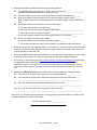
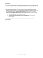
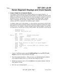
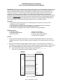
CET335 Microprocessor Interfacing
Lab 5: LCD Interface (Bus Attached Peripheral)
Introduction: In this lab, you will learn the interface and operation of a “bus-attached” peripheral; in other
words, a controller IC that normally connects directly to the system buses. The controller you will learn
about is the Hitachi HD44780 Liquid Crystal Display Controller (LCDC) as found on-board the LCD
module used in this lab. You will become familiar with both the hardware interface and the software
required to control and operate the display via the LCDC. Because the software for this device is
somewhat more complex than previous labs, you will be given a collection of low-level control routines in
the form of a software driver and you will learn how to use this driver from your application program. Of
particular note in this lab is the fact that because the S12 MCU on board the Dragon12 EVB does not
have external buses, you will see that all LCD interfacing is done via PORTK I/O lines.
Objectives:
• to provide the student an exposure to a complex peripheral controller IC as used for LCD
applications and of its datasheet
• to demonstrate the interface and synchronization of a bus-attached peripheral controller
• to demonstrate the software control of a peripheral controller IC
• to demonstrate a single-point entry method of software driver implementation
Materials needed:
• DRAGON12 EVB
• LCD module (preinstalled)
• pushbutton switch
•
•
•
•
Dragon12+ schematic
Dragon12+ User’s Manual
LCD-107 LCD module datasheet
HD44780 LCDC datasheet
Pre-Lab:
1. Collect your own copies of the schematic, user manual and datasheets as listed in the materials
needed section above. These documents should be available on the resources page of the course
website.
2. Review the LCD module interface diagram shown in figure 1 below. Referring to the Dragon12+
schematic (pg. 4), add the LCD PORT (J12) pin numbers just outside its box in figure 1. Next, refer to
the LCD module datasheet and add the LCD module pin numbers just outside its box in figure 1.
Q1.
Do you think this correlation was by design or just coincidence? __________
Note: this is an informal but industry-standard interface.
Dragon12
LCD PORT
PK5
LCD Module
DB7
PK2
DB0
PK1
E
PK7
R/W
PK0
RS
VO
VO
+5V
VDD
Gnd
VSS
Fig. 1: LCD interface
Lab 5: LCD Interface - Page 1
3. Review the HD44780 datasheet and answer the following questions.
Q2.
The HD44780 is an example of LSI IC. What is LSI an acronym for? ___________________
Review the HD44780 block diagram to see why this is so.
Q3.
Review the table of pin functions. How many total pins does the HD44780 have? ______
Q4.
How many characters are provided for by the internal character generator ROM? ______
Refer to table 4 and note the relationship between the character pattern codes and the ASCII
table.
Q5.
Review the section on the HD44780’s Functional Description.
a. How many registers does the LCDC have? ____
b. Name the ones that are directly programmer accessible? ___________________________
c. What is the purpose of the Busy Flag (BF)? ______________________________________
d. How many register locations in the memory map does the LCDC require? ______
Q6.
Refer to the LCDC Instruction chart in table 6.
a. How many different operations does the LCDC support? _____
b. The function set instruction code for 8-bit transfers, 2 line display and 5x8 characters is: ____
4. Review the Dragon12+ User’s Manual, table 1-1 and section 4.5, and note how the LCD is interfaced
to the S12’s port K lines. Note that in the absence of system buses, we will have to drive these pins
programmatically to control the LCD.
5. Return to the HD44780 data sheet and review table 13 to learn how 8-bit operation for a 2-line display
is conducted. Review figure 23 to become familiar with the required initialization sequence.
6. Go to Dincer’s LCD Simulator page (http://www.dinceraydin.com/djlcdsim/djlcdsim.html) and perform
the appropriate steps to display your name on the simulated LCD. Don’t forget the required
initialization sequence from figure 23 of the HD44780 data sheet! By accomplishing this, you will
understand precisely what the processor must do to produce LCD output via the LCDC. Cool stuff,
no?
7. Review the LCDdriver.asm listing as provided with this lab and answer the following questions.
Q7.
This LCD driver as given has a single entry point subroutine named: __________.
Q8.
How does the entry point routine determine what specific function the caller wants?
_________________________________________________________________________
Q9.
How does this driver accept additional parameters from the caller?
_________________________________________________________________________
Q10. How does this driver synchronize output writes with the LCDC?
_________________________________________________________________________
At this point, you should be properly prepared for working with the actual LCD module in lab! Show your
completed pre-lab to the instructor to proceed.
Pre-Lab Instructor Signoff: ______________
Lab 5: LCD Interface - Page 2
Lab Procedure:
8. You have noticed that the Dragon12+ EVB contains a backlit 16x2 LCD module preinstalled. Thus, no
actual attachment of an LCD is required as we will be using this display. Note that the Dragon12’s J5
header does support an optional external LCD (you are welcome to try connecting a larger LCD such
as the 2x40 modules we have in lab).
9. Although we could repeat step 6 on the Dragon12’s LCD, it would be unduly tedious because the
LCD’s bus interface is connected to the S12’s general purpose I/O port K. Therefore, it’s now time for
more neat software! Obtain a copy of the LCDdriver.asm file as shown in listing 1 to your work
directory. Using the template.asm file as before, create an S12 program that will output a message
of your choice to the LCD. At a minimum, your program should:
a) invoke the LINIT function to initialize the LCD module
b) invoke the LWRSTR function to output your message to the LCD
c) use the “#include” assembler pseudo-op before your END directive as documented in
the driver header
You may proceed with the last part of this lab only after successfully completing this step.
(cont’d next page)
Lab 5: LCD Interface - Page 3
Lab 5 Project Assignment
Create and demonstrate to the instructor a digital stop watch using the EVB, the LCD module and
software driver, and your ingenuity. At a minimum, your solution must track seconds and tenths of
seconds. Specifications are as follows.
a)
b)
c)
d)
use a pushbutton “run” switch between an appropriate input port and ground
display a greeting and instructions to the user via the Terminal connection (not LCD)
display a project title on line 1 of the LCD (ex: “Ultimate Watch”)
call a subroutine that you create to display the current elapsed time (initially zero) on the
far left of line 2 in an appropriate format (ex: 00.0)
Note: the LCD driver includes a function for decimal output!
e) wait for the “run” switch to go active
f) implement the following loop:
- delay 100 ms. (use the “millisecond delay” subroutine from previous labs)
- increment the appropriate elapsed time counters (tenths, seconds, etc.)
- output the updated elapsed time using your above subroutine†
- repeat this loop if the “run” switch is still active
g) display an exit message to the user via the Terminal connection
†Your time output subroutine should first reposition the LCD cursor to the beginning of line 2.
Deliverables
Submit a laboratory packet including:
1. A cover page including:
- course number & title
- lab number & title
- date submitted
- lab team member names and signatures
2. A lab write-up including the Project Requirements and a Description of Solution. These sections
should be clearly titled.
3. A section titled “Achievement of Course Outcomes” describing how this lab contributed to
fulfillment of the selected two program outcomes below. Each team member must complete this
section individually according to your major (CET or EET).
4. Documentation of software design development, i.e. flowcharts.
5. A properly commented, error-free assembly listing of your program per website instructions.
Total point value: 20
Selected program outcomes
By the time of graduation, Computer Engineering Technology students will demonstrate:
CET-Oc1: The knowledge, skills, techniques and applications of modern tools in the computer
engineering technology discipline
CET-Oc3: Technical problem solving skills, including the ability to identify problems, use appropriate
laboratory and test equipment, conduct experiments, gather data, analyze data and
produce results
By the time of graduation, Electrical Engineering Technology graduates will demonstrate:
EET-Oc1: The knowledge, skills, techniques and application of modern tools in the electrical
engineering technology discipline
EET-Oc10: The ability to analyze, design and implement analog and microprocessor systems
through a blend of theoretical and practical methods
Lab 5: LCD Interface - Page 4
Listing 1: LCD driver
* * * * * * * * * * * * * * * * * * * * * * * * * * * * * * * * * * * * *
*
*
S 1 2
L C D
D R I V E R
*
by J. Sumey
*
* The following routines collectively form a driver to control a smart
* Liquid Crystal Display as interfaced to the DRAGON12+ EVB on port K.
* This driver is for any LCD module with an on-board Hitachi HD44780
* LCD-II or equivalent controller. The 44780 requires two locations for
* its Instruction Register (IR) and Data Register (DR). All LCD
* functions are user callable via the single entry point "LCD" using
* a "function code" passed in accumulator A. Function parameters, when
* any, are passed in AccB and/or register X. This driver is code only,
* no memory-resident variables are required.
*
* Example usage:
*
ldaa #LCLEAR ;A=clear display function code
*
jsr
LCD
;clear display
*
ldaa #LWRDEC ;A=decimal output function code
*
ldab #123
;decimal number to output
*
jsr
LCD
;output decimal number
*
* Note that the "LINIT" function must be invoked to initialize the LCD
* before any other function will work. This should part of your one-time
* initialization code. To add this driver to your main program, insert
* the following line before your END statement:
* #include "LCDdriver.asm"
*
* Interfacing details:
*
PK7 = LCD R/W' (Read/Write, not used)
*
PK5 = LCD DB7
*
PK4 = LCD DB6
*
PK3 = LCD DB5
*
PK2 = LCD DB4
*
PK1 = LCD EN (Enable)
*
PK0 = LCD RS (Register Select: 0=control, 1=data)
*
* Revision history:
* 10-Feb-1990 jss
initial writing
* 02-Dec-2003 jss
revised for Axiom CME11 board
* 11-Oct-2008 jss
additional documentation added
* 20-Oct-2011 jss
revised for DRAGON12 EVB
*
* * * * * * * * * * * * * * * * * * * * * * * * * * * * * * * * * * * * *
LCDPORT
LCDDDR
RSBIT
ENBIT
RWBIT
EQU
EQU
EQU
EQU
EQU
$0032
$0033
1
2
$80
*
*
*
*
*
*
*
*
*
*
*
*
*
*
*
*
*
*
*
*
*
*
*
*
*
*
*
*
*
*
*
*
*
*
*
*
*
*
*
*
*
*
*
*
;PORTK
;DDRK
;bit mask for RS
;for ENable pulse
;for Read/Write line
***************************************************************************
*
LCD DRIVER ROUTINE FUNCTION CODES
*
***************************************************************************
*
*
*
*
The following definitions define symbolic names for LCD functions
available in this driver. The desired function code is loaded into
AccA before a JSR to LCD is executed. Some functions additionally
require other parameters in AccB and/or X.
LINIT
LCLEAR
LHOME
LGOTO
LWRCMD
LWRCHR
LWRSTR
LWRDEC
LWRHEX2
LWRHEX4
EQU
EQU
EQU
EQU
EQU
EQU
EQU
EQU
EQU
EQU
0
1
2
3
4
5
6
7
8
9
;initialize display function
;clear display function
;home cursor function
;move cursor to row (Xhi), column (Xlo)
;write LCD command (in B)
;write character (in B)
;write null terminated string (X points to)
;write byte (in B) as decimal
;write byte (in B) as 2 hex digits
;write word (in X) as 4 hex digits
***************************************************************************
*
LCD DRIVER ROUTINE MAIN ENTRY
*
Lab 5: LCD Interface - Page 5
***************************************************************************
*
*
*
*
*
On entry to LCD via JSR, AccA contains the desired function number and
is used (after doubling) as an offset into a vector table to call the
corresponding routine. This works much like a computed GOSUB so that
only a single entry point for all LCD functions is needed.
All registers (except CC) are preserved for the caller.
;
LCD
LCDEX
ORG
pshy
pshx
pshd
asla
cmpa
bhs
ldy
exg
ldy
jsr
puld
pulx
puly
rts
$1100
;or where ever you want (optional)
;save caller's registers
#LCDTBLLEN
LCDEX
#LCDJMPTBL
A,B
B,Y
0,Y
;double function number
;is function number invalid?
;return immediately if not
;point Y to jump table
;swap A & B
;get address of routine
;call function handler
;restore caller's registers
;and return to caller
*** Jump Table - contains 2 byte address for each function handler ***
LCDJMPTBL FDB
FDB
FDB
FDB
FDB
FDB
FDB
FDB
FDB
FDB
LCDTBLLEN EQU
LCDINIT
LCDCLEAR
LCDHOMECU
LCDGOTORC
LCDWRCMD
LCDWRCHR
LCDWRSTR
LCDWRDEC
LCDWRHEX2
LCDWRHEX4
*-LCDJMPTBL
;0 = initialize display
;1 = clear display
;2 = home cursor
;3 = goto row, column
;4 = write LCD instruction
;5 = write LCD data character
;6 = write character string
;7 = write byte as decimal
;8 = write byte as 2 hex digits
;9 = write word as 4 hex digits
;length of jump table in bytes
LCDITBL
FCB
6
;number of table entries
FCB
$33
;1st reset code, must delay 4.1ms after sending
; all following 10 nibbles must be delay 40us min each after sending
FCB
$32
;3rd/4th reset code,
FCB
$28
;4 bit mode, 2 line, 5X7 dot
FCB
$06
;cursor INCrement, disable display shift
FCB
$0C
;display on, cursor off, no blinking
FCB
$01
;clear display memory, set cursor to home pos
*** INITLCD: initialize display ***
LCDINIT
LCDILOOP
clr
movb
ldx
ldab
ldaa
psha
rora
rora
lbsr
lbsr
pula
rola
rola
lbsr
lbsr
dbne
rts
LCDPORT
#$FF,LCDDDR
#LCDITBL
1,X+
1,X+
;initial outputs all low
;make LCD port all outputs
;point X to LCD initialization table
;get length of table
;get init code from table
;move top nibble into position
LCDWRNIB
Delay5ms
;send 4-bit nibble to LCD
;5ms delay between all table values
;move bottom nibble into position
LCDWRNIB
Delay5ms
B,LCDILOOP
;send 4-bit nibble to LCD
;5ms delay between all table values
*** LCDCLEAR: clear display to blanks and home cursor ***
LCDCLEAR
ldaa
bsr
#1
LCDWRCMD
;clear display instruction
*** LCDHOMECU: return cursor to home position ***
LCDHOMECU ldaa
bsr
lbsr
#2
LCDWRCMD
Delay5MS
;return home instruction
Lab 5: LCD Interface - Page 6
rts
***
*
*
*
LCDGOTORC: move cursor to row, column
Stacked Xhi is target row (0..1), Xlo is column (0..39)
For a 2-line LCD, RAM addresses $80..$BF are for line 0
while $C0..$FF are for line 1.
LCDGOTORC ldaa
ldab
mul
ldaa
aba
oraa
bra
4,S
#%01000000
5,S
#%10000000
LCDWRCMD
;pick row from stack
;B=2^6
;calculate row address
;pick column from stack
;add row*64 to col
;make "set RAM addr" command
;go write it & return
*** LCDWRDEC: write byte in AccA as unsigned decimal number
LCDWRDEC
LCDWRDEC2
LCDWRDEC3
LCDWRDEC4
LCDWRDEC5
tab
clra
ldx
idiv
pshb
xgdx
ldx
idiv
pshb
xgdx
tba
beq
bsr
pula
tsta
bne
tstb
beq
bsr
pula
bra
;B=number to output
#10
;X = divisor
;D = D rem 10, X = D DIV 10
;save units
;exchange rem & quotient
;now get tens
#10
LCDWRDEC3
LCDWRHEX1
LCDWRDEC4
LCDWRDEC5
LCDWRHEX1
LCDWRHEX1
;save tens
;get hundreds in D
;move to A & setup Z
;suppress if 0
;output hundreds digit
;restore tens
;was it 0?
;output it if not
;was hundreds 0?
;suppress tens if so
;output tens digit
;restore units digit
;output it & return
*** LCDWRHEX4: write word as 4 hex digits
*
stacked X is 16 bit word to output
LCDWRHEX4 ldd
bsr
tba
4,S
LCDWRHEX2
;pick X from stack
;output A as hex
;output B as hex & return
*** LCDWRHEX2: write byte in AccA as 2 hex digits
LCDWRHEX2 psha
lsra
lsra
lsra
lsra
bsr
pula
LCDWRHEX1 anda
adda
daa
adca
daa
bra
;save original byte
;move hi nibble to lo
LCDWRHEX1
#$0F
#$90
#$40
LCDWRCHR
;output hi nibble
;recall & output lo half
;mask off top nibble
;now A=$90..$9F
;$90..$99 or 00..05+Carry
;$D0..$D9 or $41..$46
;$30..$39 or $41..$46 => ASCII!
;output as ASCII & return
*** LCDWRSTR: write a character string to LCD ***
*
X points to beginning of null-terminated string
LCDWRSTR
LCDWRSEX
ldaa
beq
bsr
inx
bra
rts
0,X
LCDWRSEX
LCDWRCHR
;pick up a chr from string
;exit if end-of-string
;else output it
;bump string ptr.
;repeat
LCDWRSTR
*** WRCHR: write a data byte to LCD ***
LCDWRCHR
bset
bra
LCDPORT,RSBIT
LCDWRBYTE
;set RS bit to LCD high
Lab 5: LCD Interface - Page 7
*** WRCMD: write an instruction to LCD ***
LCDWRCMD
bclr
LCDPORT,RSBIT
;set RS bit to LCD low
;& fall thru to LCDWRBYTE
*
*** lowest-level LCD output routines using I/O port ***
*
; LCDWRBYTE: output AccA value to LCD in 4-bit mode
LCDWRBYTE psha
;save original value
rora
;move top nibble into position
rora
bsr
LCDWRNIB
;send it
pula
;recall original value
rola
;move low nibble into position
rola
bsr
LCDWRNIB
;send it
bsr
Delay50us
;minimal output delay
rts
; LCDWRNIB: output middle 4 bits of AccA to LCD
LCDWRNIB anda
#$3C
;extract middle 4 bits to write
psha
;save on stack
ldaa
LCDPORT
;read current output pattern
anda
#$C3
;clear middle 4 bits
oraa
1,SP+
;turn on needed bits
staa
LCDPORT
;send to LCD
; LCDENPLS: send Enable pulse to LCD
LCDENPLS psha
bset
LCDPORT,ENBIT
ldaa
#8
dbne
A,*
bclr
LCDPORT,ENBIT
pula
rts
;preserve A
;drive enable line high
;count for 1us delay
;hold it a while
;return to low
* Delay5ms: delay 5 millisecond via software,
*
assumes F=24 MHz (and no interrupts)
*
all registers preserved for caller
Delay5ms pshx
;2~ preserve registers used here
ldx
#39996
;2~ iterations for 5ms.
dbne
X,*
;3~ 39996 loops * 3~/loop = 119988~
pulx
;3~ recover used registers
rts
;5~ 119988 + 12 = 120000~ = 5ms.
Delay50us:
pshx
ldx
dbne
pulx
rts
#396
X,*
;2~
;2~
;3~
;3~
;5~
preserve registers used here
iterations for 50us.
396 loops * 3~/loop = 1188~
recover used registers
1188 + 12 = 1200~ = 50us.
***************************************************************************
*
End of LCD Driver
*
***************************************************************************
Lab 5: LCD Interface - Page 8