1
- 51 -
LEON2 XST User’s Manual
8.5 SRAM access
The SRAM area can be up to 1 Gbyte, divided on up to five RAM banks. The size of banks
1-4 (RAMSN[3:0]is programmed in the RAM bank-size field (MCR2[12:9]) and can be set
in binary steps from 8 Kbyte to 256 Mbyte. The fifth bank (RAMSN[4]) decodes the upper
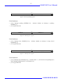
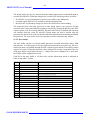
512 Mbyte. A read access to SRAM consists of two data cycles and between zero and three
waitstates. Accesses to RAMSN[4] can further be stretched by de-asserting BRDYN until the
data is available. On non-consecutive accesses, a lead-out cycle is added after a read cycle to
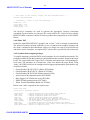
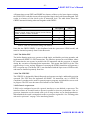
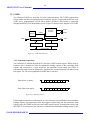
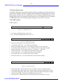
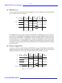
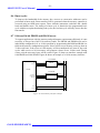
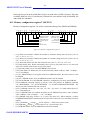
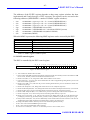
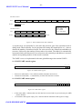
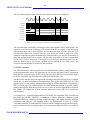
prevent bus contention due to slow turn-off time of memories or I/O devices. Figure 37 shows
the basic read cycle waveform (zero waitstate).
data1
data2
lead-out
CLK
A
A1
RAMSN
RAMOEN
D
D1
Figure 37: Static ram read cycle (0-waitstate)
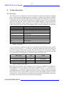
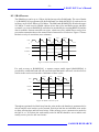
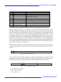
For read accesses to RAMSN[4:0], a separate output enable signal (RAMOEN[n]) is
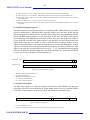
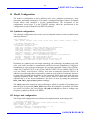
provided for each RAM bank and only asserted when that bank is selected. A write access is
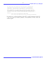
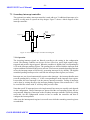
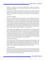
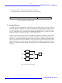
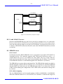
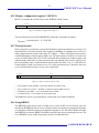
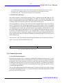
similar to the read access but takes a minimum of three cycles:
lead-in
data
lead-out
CLK
A
A1
RAMSN
RWEN
D
D1
Figure 38: Static ram write cycle
Through an (optional) feed-back loop from the write strobes, the data bus is guaranteed to be
driven until the write strobes are de-asserted. Each byte lane has an individual write strobe
to allow efficient byte and half-word writes. If the memory uses a common write strobe for
the full 16- or 32-bit data, the read-modify-write bit MCR2 should be set to enable readmodify-write cycles for sub-word writes.
GAISLER RESEARCH