1
DKAN0000B
NXP LPC21/23xx Quick Start
09 September 2008
Features
•
•
•
Phase Locked Loop (PLL)
Memory Accelerator Module (MAM)
Vectored Interrupt Controller (VIC)
Introduction
This application note is a guide to quickly start a new project with the LPC21/23xx family of ARM7
devices from NXP. It describes a procedure for initializing the PLL, MAM, and VIC to realize the full
capabilities of this processor. When enabled, the PLL speeds up the core and allows internal clock
adjustments. The MAM enhances the core throughput by limiting cache misses and prefetching
instructions and data. The VIC facilitates the programmable assignment and reassignment of multiple
interrupt sources and their priority levels.
This application note and accompanying source code include everything essential to set up the PLL,
MAM, and VIC. The code, written in ANSI C, compiles with multiple newlib-based ARM GCC builds
(e.g. GNUARM, CodeSourcery, YARGATO). Other C compilers, such as IAR and Keil, can use the
same function routines—given appropriate changes to the header files and startup scripts.
Application
Phase Locked Loop (PLL)
The PLL is a control system that generates a range of output frequencies from an input frequency. The
PLL includes a current controlled oscillator (CCO) and a clock divider, which scale the output frequency
to meet the system requirements. Increasing the clock speed improves performance, whereas decreasing
the clock speed lowers power consumption.
The PLL can only be enabled by software. This software routine configures and activates the PLL, waits
for it to lock, and connects it to the system clock. Internal circuitry synchronizes the transition between
the external oscillator and the PLL output (or vice versa) to eliminate glitches.
LPC21xx Family
The PLL is set up with the PLL Configuration (PLLCFG) and the PLL Control (PLLCON) registers. The
PLLCFG register contains the PLL multiplier and divider values. PLLCON controls the enable and
connect functionality of the PLL hardware’s logic. Finally, a PLL feed sequence puts PLLCON and
PLLCFG changes into effect. This process is implemented as follows:
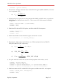
1) Determine the multiplier and divider values for the PLLCFG register (MSEL and PSEL).
Page 1 of 7
NXP LPC21/23xx Quick Start
Fsysclk
(1)
MSEL =
(2)
156
320
≤ PSEL ≤
∴ PSEL : (1,2,4,8)
2 × Fsysclk
2 × Fsysclk
Fosc
∴1 ≤ MSEL ≤ 32
2) Update the PLLCFG register bits to correspond with these MSEL and PSEL values, as specified in
the LPC21xx User Manual for the desired Fosc. Then, execute a PLL feed sequence to latch this
configuration.
PLLCFG = (options->MSEL | options->PSEL);
PLLFEED = 0xAA;
PLLFEED = 0x55;
3) Enable the PLL with the PLLCON register, and follow with a PLL feed sequence.
PLLCON = PLLCON_PLLE;
PLLFEED = 0xAA;
PLLFEED = 0x55;
4) Monitor the PLOCK bit in the PLLSTAT register until the PLL is locked.
while(!(PLLSTAT & (1 << PLLSTAT_PLOCK)));
5) Enable and connect the PLL with the PLLCON register, and follow with a PLL feed sequence.
PLLCON = (PLLCON_PLLE | PLLCON_PLLC);
PLLFEED = 0xAA;
PLLFEED = 0x55;
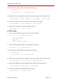
6) Determine the required Advanced Peripheral Bus (APB) divider value (APB_DIV).
(3)
FABP =
Fosc
∴ APB _ DIV : (1,2,4)
APB _ DIV
7) Setup the divider value required for the APB.
APBDIV = options->APB_DIV;
LPC23xx Family
There are a number of differences between the LPC21xx and LPC23xx PLLs, which require minor
changes to the PLL algorithm, (Note: consult the errata sheets for the core revision, and make changes
where appropriate.)
1) Start the main oscillator with the SCS register, and wait for it to stabilize.
SCS |= (1 << SCS_OSCEN);
while(!(SCS & (1 << SCS_OSCSTAT)));
2) Select the clock source.
Digi-Key Corporation
Page 2 of 7
NXP LPC21/23xx Quick Start
CLKSRCSEL = options->CLKSRC;
3) Determine the multiplier and divider values for the PLLCFG register (MSEL and NSEL) to meet the
core’s requirement for Fcco.
(4)
Fcco =
2 × MSEL × Fosc
NSEL
4) Update the PLLCFG register bits to correspond with these MSEL and NSEL values, as specified in
the LPC23xx User Manual for the desired Fcco. Then, execute a PLL feed sequence to latch this
configuration.
PLLCFG = (options->MSEL | options->NSEL);
PLLFEED = 0xAA;
PLLFEED = 0x55;
5) Enable the PLL with the PLLCON register, and follow with a PLL feed sequence.
PLLCON = PLLCON_PLLE;
PLLFEED = 0xAA;
PLLFEED = 0x55;
6) Monitor the PLOCK bit in the PLLSTAT register until the PLL is locked.
while(!(PLLSTAT & (1 << PLLSTAT_PLOCK)));
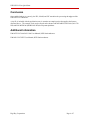
7) Determine the divider values required for the core, USB and peripheral clocks (CLK_DIV,
USB_DIV, and PCLK_DIV, respectively).
Fosc
∴ Fcpu ≤ Fcpu , max
CLK _ DIV
(5)
Fcpu =
(6)
USB _ DIV =
(7)
FPERH =
Fosc
Fosc
=
Fusb 48MHz
Fosc
∴ PCLK _ DIV : (1,2,4,8)
PCLK _ DIV
8) Set up the final CPU clock divider (and the USB and peripheral clock dividers, if used).
CCLKCFG = options->CLK_DIV;
USBCLKCFG = options->USB_DIV;
PCLKSEL0 = (options->PCLK_PERH_DIV_1 << options->PCLK_PERH_A);
PCLKSEL1 = (options->PCLK_PERH_DIV_2 << options->PCLK_PERH_B);
9) Enable and connect the PLL with the PLLCON register, and follow with a PLL feed sequence.
PLLCON = (PLLCON_PLLE | PLLCON_PLLC);
PLLFEED = 0xAA;
PLLFEED = 0x55;
Digi-Key Corporation
Page 3 of 7
NXP LPC21/23xx Quick Start
Memory Accelerator Module (MAM)
The MAM is an interface designed to speed up flash execution by providing the next ARM instruction to
prevent core fetch stalls. It eliminates the need to wait for most flash memory fetches. However, in the
event of a cache miss, the delay is still only limited by the number of MAM fetch cycles required. The
LPC21xx flash memory is split into dual banks, accessed independently. Each bank has its own 128-bit
prefetch and branch trail buffers. In 32-bit ARM mode, these buffers can provide 4 instructions per fetch.
The LPC23xx has a single bank of flash memory and three 128-bit buffers (prefetch, branch trail, and
data).
The MAM has three modes of operation. In mode 0, the MAM is off, and every memory request initiates
a flash fetch. Mode 1 partially enables the MAM. A fetch is initiated whenever there is no data in the
latches or the memory request is non-sequential. Otherwise, the latched data is used. The MAM is fully
enabled in mode 2, and a fetch executes only if the latches lack data. Mode 2 provides the best
performance but offers the least predictability.
1) To set up the MAM, clear the MAM Control register (MAMCR).
MAMCR = 0;
2) Update the MAM Timing Control register (MAMTIM) with the number of flash wait cycles required
for the specified clock speed. (Note: consult the user manual, “MAM usage notes” to determine the
recommended number of fetch cycles at a given Fosc.)
MAMTIM = options->TIMING;
3) Finally, the MAM Control register is updated with the required mode.
MAMCR = options->MODE;
Vectored Interrupt Controller (VIC)
Internally, the ARM core only has two interrupt inputs: Interrupt Request (IRQ) and Fast Interrupt
Request (FIQ). FIQs have higher priority than IRQs. Assigning only one FIQ results in the fastest
interrupt response. The VIC facilitates the programmable assignment and reassignment of multiple
interrupt sources and their priority levels.
LPC21xx Family
1) For each required interrupt, set its type, priority, and return address.
static const vic_t EXAMPLE_Settings =
{
.ISR = VIC_EXAMPLE,
.FIQ = 0,
.PRIORITY = 0,
.ADDR = (uint32_t)example
};
2) Clear the selected interrupt with the Interrupt Enable Clear register.
VICIntEnClr |= (1 << options->ISR);
Digi-Key Corporation
Page 4 of 7
NXP LPC21/23xx Quick Start
3) Define interrupt as FIQ or IRQ via the Interrupt Select register.
if (options->FIQ)
{
VICIntSelect |= (1 << options->ISR);
}
4) Enable the Vector Control register with the selected priority and specify the interrupt source.
*(&VICVectCntl0 + options->PRIORITY) = (VIC_ENABLE | options->ISR);
5) Add the return address to the Vector Address register with the same priority.
*(&VICVectAddr0 + options->PRIORITY) = options->ADDR;
6) Enable selected interrupt with the Interrupt Enable register.
VICIntEnable |= (1 << options->ISR);
LPC23xx Family
1) For each required interrupt, set its type, priority, and return address.
static const vic_t EXAMPLE_Settings =
{
.ISR = VIC_EXAMPLE,
.FIQ = 0,
.PRIORITY = 0,
.ADDR = (uint32_t)example
};
2) Clear the selected interrupt with the Interrupt Enable Clear register.
VICIntEnClr |= (1 << options->ISR);
3) Define interrupt as FIQ or IRQ via the Interrupt Select register.
if (options->FIQ)
{
VICIntSelect |= (1 << options->ISR);
}
4) Enable the Vector Control register with the selected interrupt source and specify the priority.
*(&VICVectPriority0 + options->ISR) = options->PRIORITY;
5) Add the return address to the Vector Address register with the same interrupt source.
*(&VICVectAddr0 + options->ISR) = options->ADDR;
6) Enable selected interrupt with the Interrupt Enable register.
VICIntEnable |= (1 << options->ISR);
Digi-Key Corporation
Page 5 of 7
NXP LPC21/23xx Quick Start
Conclusion
Once enabled and set up correctly, the PLL, MAM, and VIC maximize the processing throughput of the
NXP LPC21/23 ARM core.
A zip file is included with the application note; it contains an example project that applies the features
discussed above. The example code was developed and evaluated with the IAR KS LPC2106 (568-1756ND) and Keil MCB2300 (MCB2360U-ND) development platforms.
Additional Information
UM10275 LPC2104/2105/2106 User Manual; NXP Semiconductors.
UM10211 LPC23XX User Manual; NXP Semiconductors.
Digi-Key Corporation
Page 6 of 7
NXP LPC21/23xx Quick Start
Disclaimer
This document is for informational use only and is subject to change without prior notice. Digi-Key makes no commitment to
update or keep current the information contained herein. Digi-Key does not guarantee or warrant that any information provided
is accurate, complete, or correct and disclaims any and all liability associated with the use of the information contained herein.
The use of this information and Digi-Key’s liability is subject to Digi-Key’s standard Terms & Conditions which can be found at
www.digi-key.com by clicking on the Terms & Conditions link at the bottom of the web page.
No license, whether express, implied, arising by estoppel or otherwise is granted under any intellectual property or other rights of
Digi-Key or others.
Trademarks
DIGI-KEY® is a registered trademark of Digi-Key Corporation. All other trademarks, service marks and product names
contained herein are the sole property of their respective owner and their use is for informational purposes only and does not
imply any endorsement, recommendation, sponsorship or approval by the trademark owner of the contents.
Copyright
Use of this document is limited to customer’s internal business use for the evaluation and purchase of
products. No permission is granted to the user to copy, print, store, distribute, transmit, display in public or
modify the content of this document in any way for any other purpose.
© Copyright 2009 Digi-Key Corporation. All rights reserved.
Digi-Key Corporation
Page 7 of 7