1
AEROFLEX GAISLER
596
GRIP
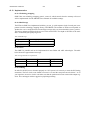
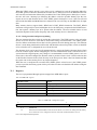
timing problems with the output delay when a separate SDRAM bus is used. SDRAM bus signals are
described in section 59.13, for configuration options refer to section 59.15.
59.9.11 Clocking
The SDRAM clock typically requires special synchronisation at layout level. For Xilinx and Altera
device, the GR Clock Generator can be configured to produce a properly synchronised SDRAM
clock. For other FPGA targets, the GR Clock Generator can produce an inverted clock.
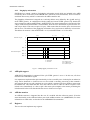
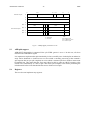
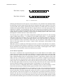
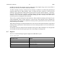
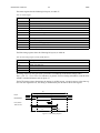
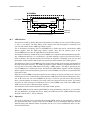
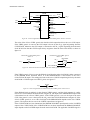
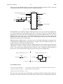
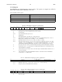
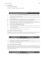
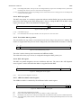
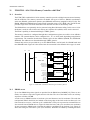
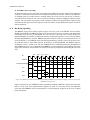
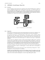
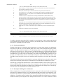
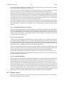
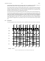
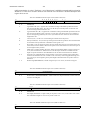
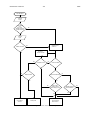
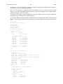
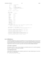
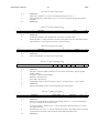
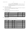
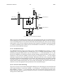
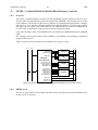
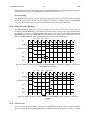
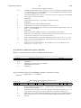
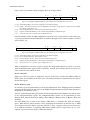
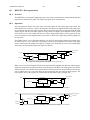
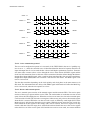
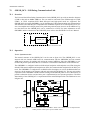
59.10 Using bus ready signalling
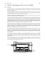
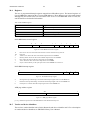
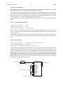
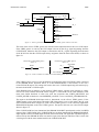
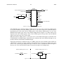
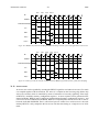
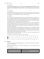
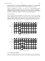
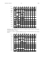
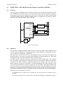
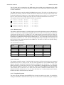
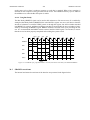
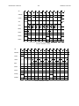
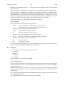
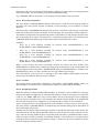
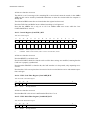
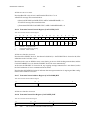
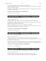
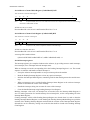
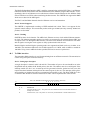
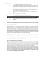
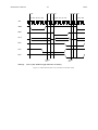
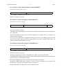
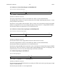
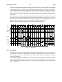
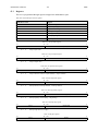
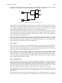
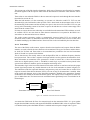
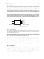
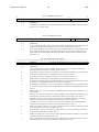
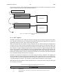
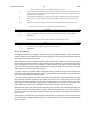
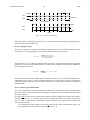
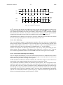
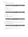
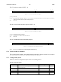
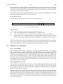
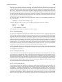
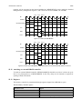
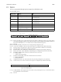
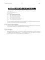
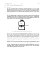
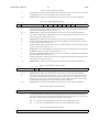
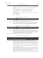
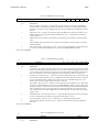
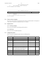
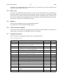
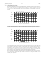
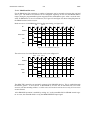
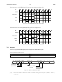
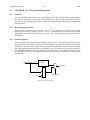
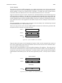
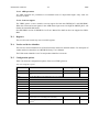
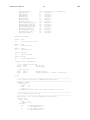
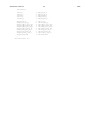
The MEMI.BRDYN signal can be used to stretch access cycles to the I/O area and the ram area
decoded by MEMO.RAMSN[4]. The accesses will always have at least the pre-programmed number
of waitstates as defined in memory configuration registers 1 & 2, but will be further stretched until
MEMI.BRDYN is asserted. MEMI.BRDYN should be asserted in the cycle preceding the last one.
The use of MEMI.BRDYN can be enabled separately for the I/O and RAM areas.
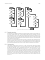
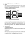
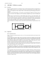
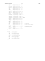
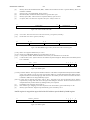
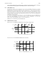
data1
data2
data2
lead-out
clk
address
A1
romsn/iosn/ramsn[4]
oen
data
D1
brdyn
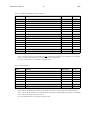
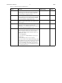
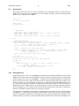
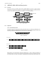
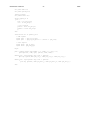
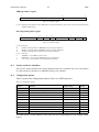
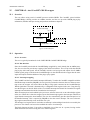
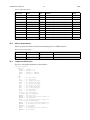
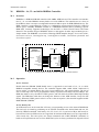
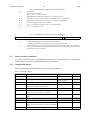
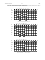
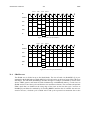
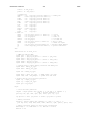
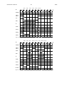
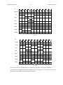
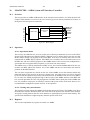
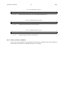
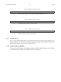
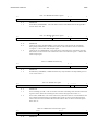
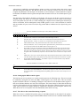
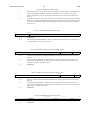
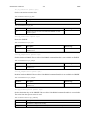
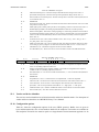
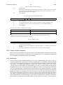
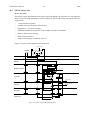
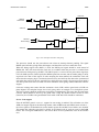
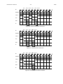
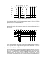
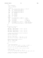
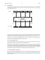
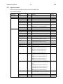
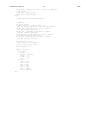
Figure 211. READ cycle with one extra data2 cycle added with BRDYN (synchronous sampling). Lead-out cycle is
only applicable for I/O accesses.
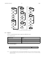
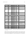
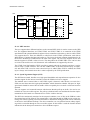
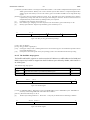
data1
clk
address
data2
data2
ws
data2
brdyn
lead-out
A1
romsn/iosn/ramsn[4]
oen
data
D1
brdyn
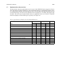
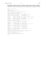
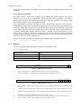
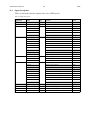
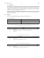
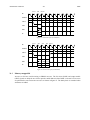
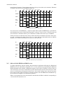
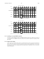
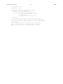
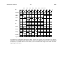
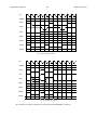
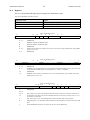
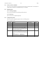
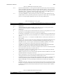
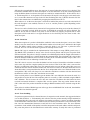
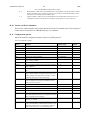
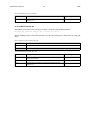
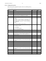
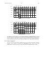
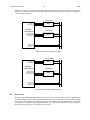
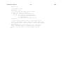
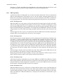
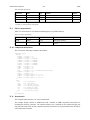
Figure 212. Read cycle with one waitstate (configured) and one BRDYN generated waitstate (synchronous
sampling).
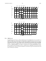
59.11 Access errors
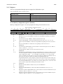
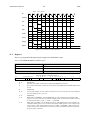
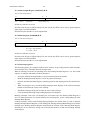
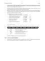
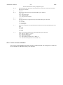
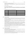
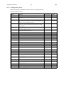
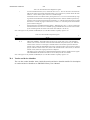
An access error can be signalled by asserting the MEMI.BEXCN signal, which is sampled together
with the data. If the usage of MEMI.BEXCN is enabled in memory configuration register 1, an error