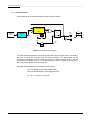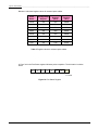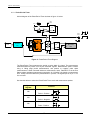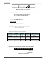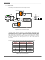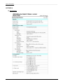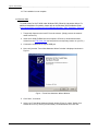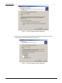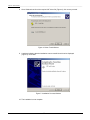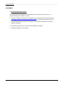
1
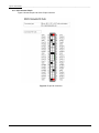
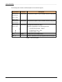
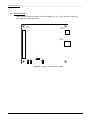
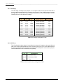
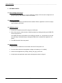
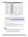
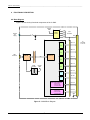
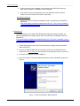
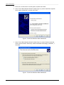
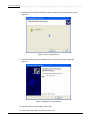
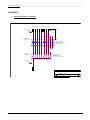
Model JI-4040
USB Multifunction Digital I/O Module - Isolated
User Manual
Version 1.2
Jupiter Instruments
JI-4040
5/7/2011 Edition
1
4/25/11
Jupiter Instruments_____________________________________________________________________________________
TABLE OF CONTENTS
1.
INTRODUCTION
4
2.
CONNECTORS AND JUMPERS
5
2.1
Connectors
2.1.1
Connector Locations
2.1.2
I/O Connector 50-pin
5
5
6
2.2
Jumper Settings
2.2.1
I/O Voltage
2.2.2
I/O Pull-up
8
9
9
3.
GETTING STARTED
10
3.1
Set I/O Voltage and Pull-ups
10
3.2
Software Installation
10
3.3
USB Driver Check
10
3.4
Software Check
10
3.5
GPIO Test
3.5.1
Output Test
3.5.2
Input Test
11
12
12
3.6
SFP Test
3.6.1
Clock and Pulse Generator
3.6.2
Pulse/Period Timer
3.6.3
Event Counter
13
14
15
16
4.
FUNCTIONAL DESCRIPTION
4.0
Block Diagram
17
17
4.1
I/O Ports
4.1.1
General Purpose I/O
4.1.2
Special Function Port (SFP)
4.1.2.1 Clock Generator
4.1.2.2 Pulse Generator
4.1.2.3 Pulse/Period Timer
4.1.2.4 Event Counter
18
19
20
21
23
25
27
APPENDIX A
1.0
29
Specifications
29
APPENDIX B
1.1
JI-4040
32
PC System Requirements
32
2
4/25/11
Jupiter Instruments_____________________________________________________________________________________
APPENDIX C
33
1.
Installing USB Device Driver
33
1.1
Windows 7
33
1.2
Windows Vista
33
1.3
Windows XP
34
1.4
Windows 2000
37
APPENDIX D
1.0
40
Installing Application Software
40
APPENDIX E
1.
41
Top Panel Removal Procedure
41
APPENDIX F
1.
42
Output Test Fixture - Schematic
42
APPENDIX G
1.
43
Input Test Fixture – Schematic
43
APPENDIX H
44
1.0 General Information
44
1.1
Warranty
44
1.2
Thirty-Day Return Policy
44
1.3
Limitation of Liability
44
1.4
Contact Us
44
JI-4040
3
4/25/11
Jupiter Instruments_____________________________________________________________________________________
1. INTRODUCTION
The JI-4040 module is a versatile, easy-to-use device for adding universal digital I/O capability to a
computer system via a USB connection. The module is comprised of 36 bidirectional I/O channels and 2
Special Function Ports (SFP). The SFP can be software programmed as a variable duty-cycle clock/pulse
generator, event counter, or interval/pulse timer. The I/O is selectable to interface 5.0 V, 3.3 V, 2.5 V, or
1.8 V systems. Host to module isolation eliminates ground-loops and provides protection from noise and
switching transients on external signals. The JI-4040 is available as either a desktop unit or low-cost OEM
board.
The JI-4040 includes a Windows 2000/XP/7 compatible software package. This contains sample
programs and source code written in Visual C#, and an application program that provides access to all
I/O ports and control of the SFPs.
Features
•
•
36 bidirectional I/O channels – Four 8-bit and two 2-bit ports
2 Special Function Ports (SFP). Programmable functions include:
•
Event Counter
•
Pulse/Period Timer
•
Clock/Pulse Generator
•
Selectable I/O voltage: 5.0V, 3.3V, 2.5V, 1.8V, and Adj.
•
High-current I/O drive: +/-32 mA @ 5.0 V, +/-24 mA @ 3.3 V
•
Selectable I/O pull-up/pull-down resistors
•
500Vrms Isolation rating
•
USB 2.0 compatible
•
Available as either a desktop unit or low-cost OEM board.
•
Power provided via USB bus*
* Optional power supply required if combined I/O source current exceeds 300 mA
JI-4040
4
4/25/11
Jupiter Instruments_____________________________________________________________________________________
2. CONNECTORS AND JUMPERS
2.1 Connectors
Onboard connectors link the JI-4040 to external devices such as host computer (USB),
optional I/O power supply, and user specified I/O.
2.1.1 Connector Locations
3
1
2
Figure 1. Connector Locations
1. I/O Connector: 50-pin IDC, keyed (3M D2550-5002-AR)
2. USB Connector: Type ‘B’, (Molex 67068-0000)
3. External I/O Power Connector (Optional): Circular, 2.1MM
(CUI PJ-102A)
JI-4040
5
4/25/11
Jupiter Instruments_____________________________________________________________________________________
2.1.2 I/O Connector 50-pin
Figure 2 shows the pin-outs of the 50-pin connector.
Figure 2. 50-pin I/O Connector
JI-4040
6
4/25/11
Jupiter Instruments_____________________________________________________________________________________
The following table contains a brief description of the connector signals.
Signal Name
Port A <7..0>
Direction
Description
Input/Output
8-bit General Purpose I/O port. Software direction configurable.
Input/Output
2-bit General Purpose I/O port. Software direction configurable.
Input/Output
2-bit Special Function Port (SFP).
Port B <7..0>
Port C <7..0>
Port D <7..0>
Port E <1..0>
Port F <1..0>
Port G <1..0>
Port H <1..0>
Software configurable for the following functions:
1. Clock/Pulse Generator – Output
T
Vbus
a
b
l
e
Output
GND
1
-
2. Pulse/Period Timer – Input
3. Event Counter – Input
Voltage source (I/O Voltage Level)
Ground – Reference for the port signals and the Vbus supply.
Table 1. Connector Signals
JI-4040
7
4/25/11
Jupiter Instruments_____________________________________________________________________________________
2.2 Jumper Settings
Figure 3 below shows the location of the four jumpers (J2, J3, J5, and J6) used to select the
I/O voltage and I/O pull-up polarity.
50-Pin
Connector
Power
Connector
USB
Connector
J3
3 2 1
J6
J5
3
2
1
J2
3
2
1
3
2
1
Figure 3. Jumper Locations (PCB Top Side)
JI-4040
8
4/25/11
Jupiter Instruments_____________________________________________________________________________________
2.2.1 I/O Voltage
The I/O voltage is configured via jumpers J2, J3, and J5 located on the lower left hand side of
the circuit board towards the 50-pin connector (see Figure 3). If the JI-4040 enclosure is used,
see appendix F for instructions on removing the back panel to access these jumpers. Use the
following table to set the desired I/O voltage.
J2
J3
J5
Power Source
I/O Voltage
1 to 2
1 to 2
X
Internal (Standard)
5.0V
1 to 2
2 to 3
Open
Internal (Standard)
3.3V
1 to 2
2 to 3
2 to 3
Internal (Standard)
2.5V
1 to 2
2 to 3
1 to 2
Internal (Standard)
1.8V
2 to 3
1 to 2
X
External (Optional)
5.0V
2 to 3
2 to 3
Open
External (Optional)
3.3V
2 to 3
2 to 3
2 to 3
External (Optional)
2.5V
2 to 3
2 to 3
1 to 2
External (Optional)
1.8V
Table 2. I/O Voltage Configuration Table
2.2.2 I/O Pull-up
The I/O pull-up/pull-down selection is configured via jumper J6 located on the lower left hand
side of the circuit board towards the 50-pin connector (see Figure 3). If the JI-4040 enclosure
is used, see appendix E for instructions on removing the back panel to access these jumpers.
Use the table below to set the desired pull-up polarity.
J6
Configuration
1 to 2
Pull-up to Vbus
2 to 3
Pull-down to GND
Open
Float
Table 3. I/O Pull-up/Pull-down Configuration Table
JI-4040
9
4/25/11
Jupiter Instruments_____________________________________________________________________________________
3. GETTING STARTED
3.1 Set I/O Voltage and Pull-ups
If you have not already done so, set the JI-4040 I/O voltage to 5.00 volts and configure the I/O
pull-up for pull-up. See section 2.2 and 2.3 for details.
3.2 Software Installation
A USB driver as well as test software will be installed. Refer to appendix C and D for step-bystep installation instructions.
3.3 USB Driver Check
1. Connect the JI-4040 to the host PC using the 6’ USB cable.
2. After a few seconds, confirm that the JI-4040 is powered by verifying that the green PWR LED
on the rear panel is on.
If the PWR LED does not illuminate or if the LED goes out after 10 – 20 seconds, an error has
occurred. Begin troubleshooting by verifying that USB driver is installed. See appendix C for
details.
3. The USB Drive/HW Check has passed.
3.4 Software Check
1. Ensure that the JI-4040 unit is connected to the host PC and power is on.
2. Go to the folder where the test application software is installed (ex. C:/JI-4040/)
3. Launch the test application by clicking JI-4040_Test_App_VerXX.exe.
4. Verify that the test application main window is displayed as shown in figure 4.
JI-4040
10
4/25/11
Jupiter Instruments_____________________________________________________________________________________
Figure 4. JI-4040 Test Application Main window
If an error occurs and the window does not appear, begin by verifying that the .NET
Framework is installed on the host PC. To do this, click Start on your windows desktop, select
Control Panel, and then double-click the Add or Remove Programs icon. When the window
appears, scroll through the list of installed programs. Verify that the .NET Framework 3.0 (or
higher) is listed. If not, go to http://msdn2.microsoft.com/en-us/netframework/aa569263.aspx
for instructions on downloading and installing the latest .NET Framework version.
5. At the main window, open a USB port by clicking the Open button in the USB Connection
group.
6. At the menu bar, open the About message box.
7. Verify that the version numbers for the HW Version and VHDL Version are valid (i.e. HW
Version: 1.0, VHDL Version: 2.1, etc.) If a question mark (HW Version: ?, or VHDL Version: ?)
or some other character appears, an error has occurred.
8. If no errors have occurred (or if errors have been resolved) the Software Check has passed.
.
3.5 GPIO Test
This exercise verifies GPIO operation and familiarizes the user with the four 8-bit, and two 2bit GPIO ports. Required equipment to complete this exercise is listed below:
1. Output Test Fixture (see appendix F) or an oscilloscope or DVM.
2. Input Test Fixture (see appendix G) or a set of 8 jumper wires.
3. JI-4040 test application software (JI-4040_Test_App_VerXX.exe)
JI-4040
11
4/25/11
Jupiter Instruments_____________________________________________________________________________________
3.5.1 Output Test
Complete the following steps:
A. Setup
1. Remove JI-4040 power by disconnecting the USB cable.
2. Ensure that the JI-4040 I/O voltage is set to 5.00 volts and the I/O pull-up is configured for
pull-up. (See section 2.2 for details)
3. Connect the Output Test Fixture to Port A.
1. Connect the test fixture GND lead a convenient ground pin on the 50-pin connector
(See figure 2).
2. Connect the 8 LED leads to corresponding port pins (i.e. LED-0 connects to port A-0)
4. Connect the JI-4040 to the host PC.
5. Launch the JI-4040 test application and open the USB-port.
B. Run Test
1. At the main window, set ports A –F to output by clicking the Output button in the Data
Direction grouping for each port.
2. Set port A to 55h by writing 55h to the port A write text box in the Red/Write grouping, followed
by clicking the Write button.
3. Verify that every other LED is illuminated beginning at LED-1. Specifically, LEDs 0, 2, 4, and 6
are on, and LEDs 1, 3, 5 and 7 are off.
4. Now, change port A data to AAh (i.e. repeat step B-2).
5. Verify that every other LED is illuminated beginning at LED-2. Specifically, LEDs 1, 3, 5 and 7
are on and LEDs 0, 2, 4 and 6 are off.
6. Port A Output Test is complete.
C. Test remaining ports B – F
1. Next, repeat step A and B for the remaining 5 ports (B – F), moving the test fixture to each
port. For ports E and F, only connect LEDs 0 and 1.
2. If no errors were encountered in the above steps, the Output Test has passed
3.5.2 Input Test
Complete the following steps:
A. Setup
1. Remove JI-4040 power by disconnecting the USB cable.
JI-4040
12
4/25/11
Jupiter Instruments_____________________________________________________________________________________
2. Ensure that the JI-4040 I/O voltage is set to 5.00 volts and the I/O pull-up is configured for
pull-up. (See section 2.2 for details)
3. Connect the Output Input Test Fixture to Port A.
1. Connect the test fixture GND lead a convenient ground pin on the 50-pin connector
(See figure 2).
2. Connect the 8 DIP switch leads to corresponding port pins (i.e. SW-0 connects to
portA-0)
4. Connect the JI-4040 to the host PC.
5. Launch the JI-4040 test application and open the USB-port.
B. Run Test
1. At the main window, set ports A –F to input by clicking the Input button in the Data Direction
grouping for each port.
2. At the Input Test fixture, alternately switch every other switch on beginning at SW-0.
Specifically, SW-0, 2, 4, and 6 are on, and SW-1, 3, 5, 7 are off.
3. Read port A by clicking the Read button for port A in the Red/Write grouping.
4. Verify that port A reads 55h.
5. Now, change test fixture settings such that every other switch is on beginning at SW-1.
Specifically, SW-1, 3, 5, 7 are on, and SW-2, 4, 6, and 8 are off.
6. Verify that port A reads AAh.
7. Port A Input Test is complete.
C. Test remaining ports B – F
1. Next, repeat step A and B for the remaining 5 ports, moving the test fixture to each port. For
ports E and F, only connect switches SW-0 and SW-1. Substitute the value 1 for 55h in step
B-2 and 2 for AAh in step B-6.
2. If no errors were encountered in the above steps, the Input Test has passed
3.6 SFP Test
This exercise verifies SFP operation and familiarizes the user with the four operational modes:
1. Clock Generator
2. Pulse Generator
3. Pulse/Period Timer
4. Event Counter
Required equipment to complete this exercise is listed below:
1. Output Test Fixture (see appendix F) or an oscilloscope or DVM.
2. 1 jumper wire.
3. JI-4040 test application software (JI-4040_Test_AppXX.exe)
JI-4040
13
4/25/11
Jupiter Instruments_____________________________________________________________________________________
3.6.1 Clock and Pulse Generator
Complete the following steps:
A. Setup
1. Remove JI-4040 power by disconnecting the USB cable.
2. Ensure that the JI-4040 I/O voltage is set to 5.00 volts and the I/O pull-up is configured for
pull-up. (See section 2.2 for details)
3. Connect the Output Test Fixture to Port E.
1. Connect the test fixture GND lead a convenient ground pin on the 50-pin connector
(See figure 2).
2. Connect the 2 LED leads to corresponding port pins (i.e. LED-0 connects to port G-0)
4. Connect the JI-4040 to the host PC.
5. Launch the JI-4040 test application and open the USB-port.
B. Set Clock Generator to 1Hz and run test
1. At the Port G Configuration, select 10uS in the CLK Prescalar group box.
2. Begin by testing the CLK Generator. Select the CLK mode by clicking the CLK button in the
Generator group box.
3. Next, enter 500ms in both the tHIGH and tLOW text boxes.
4. Now, start the CLK by clicking the green Start button at the bottom.
5. Verify two, alternate blinking LEDs. The frequency should be 1 Hz.
6. Next, stop the CLK by clicking the red Stop button.
7. Verify that the blinking has stopped and that LED-0 is off and LED-1 is on.
8. The Clock Generator test is complete.
C. Set Pulse Generator for 500ms and run test
1. Select the Pulse Generator by clicking the Pulse button in the Generator group box.
2. Now, generate a 500mS pulse by clicking the Start button at the bottom.
3. Verify that the LED-0 is on and LED-1 is off for 500mS each time the start button is clicked.
4. The Pulse Generator test is complete.
D. Run Port H Pulse/Period Test
1. Next, repeat step A – C for port H.
2. If no errors were encountered, the port H Clock and Pulse Generator test is complete.
JI-4040
14
4/25/11
Jupiter Instruments_____________________________________________________________________________________
3.6.2 Pulse/Period Timer
Complete the following steps:
A. Setup
1. Remove JI-4040 power by disconnecting the USB cable.
2. Ensure that the JI-4040 I/O voltage is set to 5.00 volts and the I/O pull-up is configured for
pull-up. (See section 2.2 for details)
3. Connect a jumper wire from port G pin-1 to port H pin-1.
4. Connect the JI-4040 to the host PC.
5. Launch the JI-4040 test application and open the USB-port.
B. Configure Port H as a 1KHz clock source
1. At the Port H Configuration, ensure that the 1uS is selected in the CLK Prescalar group box
2. Select the CLK mode by clicking the CLK button in the Generator group box.
3. Next, enter 500us in both the tHIGH and tLOW text boxes.
4. Now, start the CLK by clicking the Start button at the bottom.
5. Port H 1KHz clock source is now running.
C. Configure Port G as a Period Timer and run test
1. At the Port G Configuration, ensure that 1uS is selected in the CLK Prescalar group box
2. Next, select period timer by clicking the Period button in the Timer group box.
3. Now, start the timer by clicking the green Start button at the bottom of the group box.
4. After a few seconds, verify that the Status reads “Done” and the Time reading is 1000uS.
5. The port G Period Timer test is complete.
D. Configure Port G as a Pulse Timer and run test
1. At the Port G Configuration, ensure that 1uS is selected in the CLK Prescalar group box
2. Next, select period timer by clicking the Pulse button in the Timer group box.
3. Now, start the timer by clicking the Start button at the bottom of the group box.
4. After a few seconds, verify that the Status reads “Done” and the Time reading is 500uS.
5. The port G Pulse Timer test is complete.
JI-4040
15
4/25/11
Jupiter Instruments_____________________________________________________________________________________
E. Run Port H Pulse/Period Test
1. Repeat steps A – D by substituting the text Port G for Port H in step B, and Port H for Port G
in steps C and D.
2. If no errors were encountered, the port H Pulse/Period Timer test is complete.
3.6.3 Event Counter
Complete the following steps:
A. Setup
1. Remove JI-4040 power by disconnecting the USB cable.
2. Ensure that the JI-4040 I/O voltage is set to 5.00 volts and the I/O pull-up is configured for
pull-up. (See section 2.2 for details)
3. Connect a jumper wire from port G pin 1 to port H pin 1.
4. Connect the JI-4040 to the host PC.
5. Launch the JI-4040 test application and open the USB-port.
B. Configure Port H as a 1000uS One-shot
1. At the Port H Configuration, ensure 1uS is selected in the CLK Prescalar group box
2. Select the CLK mode by clicking the Pulse button in the Generator group box.
3. Next, enter 1000us in the tHIGH text box.
C. Configure Port G as a Counter and run test
1. At the Port G Configuration, click the Rising Edge button in the Counter group box.
2. Next, click the enabled Always radio button.
3. Now, start the counter by clicking the Start button at the bottom of the group box.
4. Next, send 10 pulses to port H by clicking the Start button at the Port H Configuration.
5. Now, stop the counter by clicking the Stop button at the Port G Configuration.
6. Verify that the port G count reading is 10.
7. The port G Event Counter test is complete.
D. Run Port H Event Counter Test
1. Substitute the text “Port G” for “Port H” and “Port H” for “Port G” in steps A – C. Then repeat
steps A – C.
2. If no errors were encountered, the Port H Event Counter test is complete.
JI-4040
16
4/25/11
Jupiter Instruments_____________________________________________________________________________________
4. FUNCTIONAL DESCRIPTION
4.0 Block Diagram
Figure 5 shows the key functional components of the JI-4040.
Iso lat ed
PWR
5V
Bu s
Voltag e
Source
Op tion al
+5 V
Sup ply
3.3V
2.5V
1.8V
Level
Translation
Vbus
FPGA
Port A
PA.<7..0>
P1
Con nector
50- PIN IDC
8-bit
Port B
USB PHY
Galvanic Isolatio n
USB
Connector
8-bit
Serial
T ransceiver
Port C
PC.<7..0>
8-bit
Port D
DC/DC
Con verto r
PB.<7..0>
Iso lated
PWR
PD.<7..0>
8-bit
Po rt E
PE.<1,0>
2-bit
Port F
PF .< 1,0>
2-bit
Port G Special Funct ion
* Period Timer
* Event Counter
* CLK Generator
PG.<1,0>
Port H Special Funct ion
* Period Timer
* Event Counter
* CLK Generator
PH.<1,0>
GND
Figure 5. JI-4040 Block Diagram
JI-4040
17
4/25/11
Jupiter Instruments_____________________________________________________________________________________
4.1 I/O Ports
The JI-4040 is comprised of 2 port types:
1. General Purpose I/O (GPIO) 8-bit and 2-bit
2. Special Function Port
There are four, 8-bit GPIO, two, 2-bit GPIO ports and two, 2-bit Special Function Ports (SFP)
for a total of 40 I/O pins. All I/Os include a 100K resistor that is jumper configurable as either a
pull-up or pull-down (see Table 3). The I/O voltage is jumper selectable for either 5.0V, 3.3V,
2.5V, or 1.8V operation (see Table 2). Custom voltages can be selected with a single resistor
change (See Appendix TBD) or ordered custom from the factory.
JI-4040
18
4/25/11
Jupiter Instruments_____________________________________________________________________________________
4.1.1 General Purpose I/O
The JI-4040 includes 36 general purpose I/Os organized as four, 8-bit ports (A, B, C, D) and
two, 2-bit ports (E, F). Each port is assigned as either an input or output via a Data Direction
command. Upon power-up, all ports are reset to input. Commands are available to read/write
each port either individually (8-bit, byte mode) or concurrently (32-bit, long word mode) for
ports A – D. 8-bit and 2-bit GPIO block diagrams are shown in figures 6 and 7, respectively.
Write
Reg
Port
Pins
Bus
Transceiver
7
6
5
4
3
2
1
0
8-bit
Read
Reg
8-bit
DIR
Data
Direction
Reg
Figure 6. 8-Bit Port Block Diagram
Write
Reg
2-bit
Bus
Transceiver
Port
Pins
1
0
Read
Reg
2-bit
DIR
Data
Direction
Reg
Figure 7. 2-Bit Port Block Diagram
JI-4040
19
4/25/11
Jupiter Instruments_____________________________________________________________________________________
Registers
Each GPIO is individually controlled by way of three registers:
1. Data Direction Register (DDR)
2. Read Register
3. Write Register
The DDR selects the direction of data flow for the selected port. The direction is typically set
once at the beginning of a session. However, bi-directional data flow is possible by setting the
DDR for each change in direction.
As the names suggest, the Read register reads data from the port pins and the Write register
latches data to the port pins. A read or write can be performed irrespective of the DDR setting.
4.1.2 Special Function Port (SFP)
The JI-4040 includes 2 special function ports (G, H). Each port is configured in one of four
modes:
1. Clock Generator
2. Pulse Generator
3. Pulse/Period Timer
4. Event Counter
The Mode is selected via the Port Configuration Register.
Data (HEX)
Function
Operation Details
20
CLK Gen
Continuous Wave (CW)
21
Pulse Gen
One-Shot Pulse
30
Period Timer
Positive, rising-edge to rising-edge
31
Period Timer
Period, falling-edge to falling-edge
32
Pulse Timer
Pulse, rising-edge to falling-edge
33
Pulse Timer
Pulse, falling-edge to rising-edge
40
Event Counter
Rising-edge, D0 = X
41
Event Counter
Falling-edge, D0 = X
44
Event Counter
Rising-edge, Enable when D0 = 0
45
Event Counter
Falling-edge, Enable when D0 = 0
46
Event Counter
Rising-edge, Enable when D0 = 1
47
Event Counter
Falling-edge, Enable when D0 = 1
Figure 3. Port Configuration Register
JI-4040
20
4/25/11
Jupiter Instruments_____________________________________________________________________________________
4.1.2.1 Clock Generator
A block diagram of the Clock Generator is shown in figure 8 below.
EN
CLK
TH Counter
RCO
Set
16-bit
10 MHz
Clock
Q
TH
FF
Prescalar
8-bit
Port
Pins
Reset Q
EN
CLK
TL Counter
1
RCO
0
TL
16-bit
Vcc
Start
Set
Q
FF
Vcc
Reset Q
Stop
Figure 8. Clock Generator Diagram
The Clock Generator produces a variable duty-cycle, variable frequency signal with stop/start
control. The signal is output on pin 1 and the complement is available on pin 0. The Clock
Generator mode is selected by writing 20h to the configuration register of the selected port.
The frequency and duty-cycle of the clock signal is controlled by the setting of the Prescalar,
TH Counter, and TL Counter registers. Register definitions are as follows,
NTH = TH Register, valid range 0000h to ffffh
NTL = TL Register, valid range 0000h to ffffh
NPRE = Prescalar Register, valid range 00h to ffh
tH = (NTH + 1) *(NPRE + 1)*(0.1)uS
tL = (NTL + 1) *(NPRE + 1)*(0.1)uS
Using the following equations to set the CLK frequency and duty cycle
Duty Cycle
D = tH / (tH + tL)
= (NTH + 1) / ( (NTH + 1) + (NTL + 1) )
Frequency
f = 1/ (tH + tL )
7
= 10 / ( (NTH + NTL + 2)( NPRE + 1 ) ) Hz
JI-4040
21
4/25/11
Jupiter Instruments_____________________________________________________________________________________
Below are calculated register values for selected CLK frequencies and duty cycles.
Frequency
Duty
Cycle
%
Configuration
Register
Prescalar
Register
(NPRE)
TH
Register
(NTH)
TL
Register
(NTL)
5MHz
50
20h
00h
0000h
0000h
1MHz
50
20h
00h
0004h
0004h
100KHz
50
20h
09h
0004h
0004h
10KHz
50
20h
09h
0031h
0031h
10KHz
25
20h
09h
0018h
004ah
1KHz
50
20h
09h
01f3h
01f3h
100Hz
50
20h
09h
1387h
1387h
1Hz
50
20h
F9h
4e1fh
4e1fh
Table 6. Register values for selected CLK frequencies and duty cycles
JI-4040
22
4/25/11
Jupiter Instruments_____________________________________________________________________________________
4.1.2.2 Pulse Generator
A block diagram of the Pulse Generator is shown in figure 9 below.
EN
CLK
Start
STB
10 MHz
Clock
CLR
TH Counter
RCO
Set
16-bit
Q
FF
Prescalar
8-bit
Stop
Reset Q
Vcc
TH
Port
Pins
1
0
Vcc
Start
STB
Start
Figure 9. Pulse Generator Diagram
The Pulse Generator produces a single pulse with each write to the start control. The width of
the pulse is set by the Prescalar and TH Counter registers. The pulse signal can be
prematurely terminated by issuing a stop command. The signal is output on pin 1 and the
complement is available on pin 0. The Pulse Generator mode is selected by writing 21h to
the Configuration register of the selected port.
Using the following equation to set the period of the signal
NTH = TH Register, valid range 0000h to ffffh
NPRE = Prescalar Register, valid range 00h to ffh
tH = (NTH + 1) *(NPRE + 1)*(0.1)uS
JI-4040
23
4/25/11
Jupiter Instruments_____________________________________________________________________________________
Below are calculated register values for selected pulse widths.
Pulse
Width
Configuration
Register
Prescalar
Register
(NPRE)
TH
Register
(NTH)
100nS
21h
00h
0000h
1.00uS
21h
00h
0009h
10.0uS
21h
09h
0009h
50uS
21h
09h
0031h
100uS
21h
09h
0063h
1mS
21h
09h
03e7h
100mS
21h
31h
4e1fh
0.5S
21h
F9h
4e1fh
Table 5. Register values for selected pulse widths
A “Done” bit in the Port Status register indicates pulse completion. The bit location is shown
below
Bit 7
6
5
4
3
2
1
Bit 0
|
1 = Done
Figure 10. Port Status Register
JI-4040
24
4/25/11
Jupiter Instruments_____________________________________________________________________________________
4.1.2.3 Pulse/Period Timer
A block diagram of the Pulse/Period Timer is shown in figure 11 below.
Vcc
Start
STB
Start
Set
Vcc
Q
FF
Reset Q
Stop
Port
Pins
1
Configuration
Neg
10 MHz
Clock
Prescalar
Edge
Detect
0
Pos
Set
Q
EN
FF
8-bit
Neg
Start
STB
Run/Stop
Logic
Edge
Detect
CLK
CLR
T/E Counter
16-bit
Reset Q
Pos
Start
STB
Figure 11. Pulse/Period Timer Diagram
The Pulse/Period Timer measures the period or pulse width of a signal. The measurement
resolution/maximum period is set by the Prescalar register. Measurement options include
rising or falling edge period measurements, and positive or negative pulse width
measurements. A Start command initiates a measurement, and a “Data RDY” bit in the Port
Status register indicates measurement completion. An “Overflow” bit signals a measurement
error. A Stop command aborts any measurement in process. The signal input is on pin 1. Pin
0 is not used.
Use the table below to select the Pulse/Period Timer mode and measurement options.
Configuration
Register
Function
T
30h
Period – Positive
T
31h
Period – Negative
T
32h
Pulse – Positive
JI-4040
25
4/25/11
or
Jupiter Instruments_____________________________________________________________________________________
T
33h
Pulse – Negative
Table 6. Pulse/Period Timer Configuration
Use the following equations to set the resolution/maximum period of the measurement.
NPRE = Prescalar Register, valid range 00h to ffh
NT/E = T/E Register, valid range 00h to ffffh
Resolution (minimum period)
Tmin = (NPRE + 1)*0.100uS
Maximum period
Tmax = (NPRE + 1)*6.5536mS
Use the following equation to calculate the period of the signal.
T = (NPRE + 1)(NT/E)*0.100uS
Below are register values for selected configurations.
Function
Configuration
Register
Prescaler
Register
Resolution
Maximum Period
Period-positive
30h
00h
100nS
65.536mS
Period-negative
31h
09h
1uS
65.536mS
Pulse-positive
32h
63h
10uS
655.36mS
Pulse-negative
33h
67h
20uS
1.3107S
Table 7. Register values for selected configurations
Status bits for the Pulse/Period Timer are located in the Port Status Register
Bit 7
6
5
4
3
2
1
Bit 0
|
|
|
1 = Data RDY
|
1 = Overflow Error
Figure 12. Port Status Register
JI-4040
26
4/25/11
Jupiter Instruments_____________________________________________________________________________________
4.1.2.4 Event Counter
A block diagram of the Event Counter is shown in figure 13 below.
Configuration (1 of 2)
Vcc
EN = X
EN = 1
Vcc
Start
Start
STB
Set
Port
Pins
EN = 0
0
Q
Enable
FF
Vcc
EN
Reset Q
CLK
Start
STB
Stop
T/E Counter
CLR
RCO
1
16-bit
Configuration (2 of 2)
Pos
Neg
Figure 13. Event Counter Block Diagram
The Event Counter, counts the occurrence of a signal transition. Measurement options
include selection of a rising or falling edge transition and a qualification signal that enables
counting when pulled to a 1 or 0 state. A Start command initiates a measurement, and a
Stop command halts a measurement. A “Done” bit in the Port Status register indicates
measurement completion and that valid data is available at the T/E Register. An “Overflow”
bit signals a measurement error. The signal input is on pin 1. Pin 0 is the optional input
enable signal.
Use the table below to select the Event Counter mode and measurement options.
Configuration
Register
Counter Enabled
Count
Transition
40h
Always
Rising-Edge
41h
Always
Falling-Edge
42h
Bit 0 = 1
Rising-Edge
43h
Bit 0 = 1
Falling-Edge
43h
Bit 0 = 0
Rising-Edge
40h
Bit 0 = 0
Falling-Edge
Table 8. Event Counter Configuration
JI-4040
27
4/25/11
Jupiter Instruments_____________________________________________________________________________________
Status bits for the Event Counter are located in the Port Status Register
Bit 7
6
5
4
3
2
1
Bit 0
|
|
|
1 = Data RDY
|
1 = Overflow Error
Figure 14. Port Status Register
JI-4040
28
4/25/11
Jupiter Instruments_____________________________________________________________________________________
APPENDIX A
1.0 Specifications
JI-4040
29
4/25/11
Jupiter Instruments_____________________________________________________________________________________
JI-4040
30
4/25/11
Jupiter Instruments_____________________________________________________________________________________
JI-4040
31
4/25/11
Jupiter Instruments_____________________________________________________________________________________
APPENDIX B
1.1 PC System Requirements
JI-4040
•
Microsoft Windows 2000/XP/Vista or Windows 7
•
Pentium 4 or equivalent processor (600 MHz minimum)
•
USB 2.0 port
•
CD-ROM drive
•
25 MB Free hard disk space
•
256 MB Memory
32
4/25/11
Jupiter Instruments_____________________________________________________________________________________
APPENDIX C
1. Installing USB Device Driver
Two types of drivers will be installed: Virtual COM Port (VCP) and Direct Drive (D2XX). The VCP
driver allows control of the JI-4040 adapter via ASCII serial commands sent using a terminal
emulation program such as Windows Hyper Terminal. The D2XX driver allows direct access to a
USB device via a DLL interface. Both drivers are supplied by the manufacture of the USB interface
IC designed into the JI-4040. Complete USB driver information can be found at the FTDI website:
(http://www.ftdichip.com/FTDrivers.htm)
Instructions below assist with the installation of JI-4040 drivers for the following Windows
Operating systems: Windows 2000/XP/Vista or Windows 7
1.1 Windows 7
To install drivers for the JI-4040 under Windows 7, follow the instructions below:
Internet Connection
1. Ensure the host PC is connected to the internet.
2. Connect the JI-4040 to a spare USB port on the PC.
3. Windows 7 will silently connect to Windows Update website and install the required
driver(s).
4. At the conclusion of the installation, verify that the green PWR LED on the rear
panel of the JI-4040 is on. Installation is now complete.
5. If the drivers were not automatically found or the PWR LED did not illuminate,
continue to the “No Internet Connection” steps below.
No Internet Connection
1. Please refer to the FTDI Drivers Installation Guide for Windows 7 for detailed
instructions.
(http://www.ftdichip.com/Documents/AppNotes/AN_119_FTDI_Drivers_Installation_
Guide_for_Windows7.pdf)
1.2 Windows Vista
To install drivers for the JI-216 under Windows Vista, follow the instructions below:
Internet Connection
1. Ensure the host PC is connected to the internet.
1. Connect the JI-4040 to a spare USB port on the PC.
2. Vista will silently connect to Windows Update website and install the required
driver(s).
JI-4040
33
4/25/11
Jupiter Instruments_____________________________________________________________________________________
3. At the conclusion of the installation, verify that the green PWR LED on the rear
panel of the JI-4040 is on. Installation is now complete.
4. If the drivers were not automatically found or the PWR LED did not illuminate,
continue to the “No Internet Connection” steps below.
No Internet Connection
1. Please refer to the FTDI Drivers Installation Guide for Windows Vista for detailed
instructions.
(http://www.ftdichip.com/Documents/AppNotes/AN_103_FTDI_Drivers_Installation_
Guide_for_VISTA(FT_000080).pdf)
1.3 Windows XP
To install drivers for the JI-4040 under Windows XP, follow the instructions below. For
additional installation information, please refer to the FTDI Drivers Installation Guide for
Windows XP
(http://www.ftdichip.com/Documents/AppNotes/AN_104_FTDI_Driver_Installation_Guide_f
or_WindowsXP(FT_000093).pdf)
1. Temporarily disconnect the host PC from the Internet. (Simply remove the network
cable from the PC)
2. Insert the JI-4040 CD-ROM into the computer’s CD drive (or download the latest
drivers from the FTDI_Web_Site and unzip them to a temporary location on your PC.)
3. Connect the JI-4040 unit to a spare USB port.
4. Now, verify that the “Found New Hardware Wizard” window is displayed as shown in
Figure 1.
Figure 1. Found New Hardware Wizard Window
JI-4040
34
4/25/11
Jupiter Instruments_____________________________________________________________________________________
5. Select “No, not at this time” from the options, and then click “Next”.
6. At the “Found New Hardware Wizard” window (Figure 2), select “Install from a specific
list or location (Advanced)”, and then click “Next”.
Figure 2. Found New Hardware Wizard Window #2
7. At the “Found New Hardware Wizard” window (Figure 3), select “Search for the best
driver in these locations” followed by “Search removable media (floppy, CD-ROMT)”.
Click Next.
Figure 3. Found New Hardware Wizard Window #3
JI-4040
35
4/25/11
Jupiter Instruments_____________________________________________________________________________________
8. A window is now displayed showing the driver software being located and then copied
(Figure 4).
Figure 4. Driver Coping Window
9. A window indicating that the installation was successful should now be displayed
(Figure 5).
Figure 5. Installation Success Window
10. The D2XX driver is now installed. Click Finish.
11. Repeat steps 5 through 11 to install the VCP driver.
JI-4040
36
4/25/11
Jupiter Instruments_____________________________________________________________________________________
12. The installation is now complete.
1.4 Windows 2000
To install drivers for the JI-4040 under Windows 2000, follow the instructions below. For
additional installation information, please refer to the Windows 2000 Installation Guide
(http://www.ftdichip.com/Documents/InstallGuides/Windows_2000_Installation_Guide.pdf)
1. Temporarily disconnect the host PC from the Internet. (Simply remove the network
cable from the PC)
2. Insert the JI-4040 CD-ROM into the computer’s CD drive (or download the latest
drivers from the FTDI_Web_Site and unzip them to a temporary location on your PC.)
3. Connect the JI-4040 unit to a spare USB port.
4. Now, verify that the “Found New Hardware Wizard” window is displayed as shown in
Figure 1.
Figure 1. Found New Hardware Wizard Window
5. Click “Next”, to continue.
6. At the next “Found New Hardware Wizard” window (Figure 3), select "Search for a
suitable driver for my device (recommended)" as shown below, then click next.
JI-4040
37
4/25/11
Jupiter Instruments_____________________________________________________________________________________
Figure 1. Found New Hardware Wizard Window #2
7. At the next “Found New Hardware Wizard” window (Figure 4), check the box next to
"CD-ROM drives" and uncheck all others. Click next.
x
Figure 1. Found New Hardware Wizard Window #3
JI-4040
38
4/25/11
Jupiter Instruments_____________________________________________________________________________________
8. Once Windows has found the required .INF driver file (Figure 4), click next to proceed.
Figure 4. Driver Found Window
9. A window indicating that the installation was successful should now be displayed
(Figure 5). Click Next.
Figure 5. Installation Success Window
10. The installation is now complete.
JI-4040
39
4/25/11
Jupiter Instruments_____________________________________________________________________________________
APPENDIX D
1.0 Installing Application Software
The JI-4040 application software can be installed locally on the host PC’s hard drive (C:) or
executed directly from CD-ROM. To install:
2. Insert the CD-ROM into the host PC’s CD/DVD drive (or download the latest executable from (
http://www.jupiteri.com/JI-4040_Files/JI-4040_Top.html) to a temporary location on your PC.)
3. Using Windows Explorer, find the file “setup.exe” on the CD drive. Double click on the file to
begin the installation.
4. Follow the instructions on the screen until the installation is complete.
5. Software installation is now complete.
JI-4040
40
4/25/11
Jupiter Instruments_____________________________________________________________________________________
APPENDIX E
1. Top Panel Removal Procedure
TBD
JI-4040
41
4/25/11
Jupiter Instruments_____________________________________________________________________________________
APPENDIX F
1. Output Test Fixture - Schematic
LED-7 LED-6 LED-5 LED-4 LED-3 LED-2 LED-1 LED-0
Flying Lead
0.025"
Contact
Female
1
2
3
4
5
6
7
8
9
4"
10
10 segment Bar
Graph Array - LED
Part Number: DC10EWA
Manuf acture: Kingbright
Distributor: Digi-Key
Distributor PN: 754-1176-5-ND
20
19
18
17
16
15
14
13
2
3
4
5
6
7
8
9
220 Ohm SIP
Resistor Network
Flying Lead
12
11
10
Part Number: 770101221P
Manuf acture: CTS
Distributor: Digi-Key
Distributor PN: 770-101-R220P-ND
1
GND
Title
JI-4040 Output Test Fixture
Size
A
Date:
JI-4040
42
Document Number
Rev
A
SC17571
Friday , April 22, 2011
Sheet
1
of
1
4/25/11
Jupiter Instruments_____________________________________________________________________________________
APPENDIX G
1. Input Test Fixture – Schematic
SW-7 SW-6 SW-5 SW-4 SW-3 SW-2 SW-1 SW-0
Flying Lead
0.025"
Contact
Female
1
2
3
4
5
6
7
4"
8
8 Position DIP Switch
Part Number: 106-1208-EV
Manuf acture: Mountain Switch
Distributor: Mouser
Distributor PN: 106-1208-EV
16
15
14
13
12
11
10
2
3
4
5
6
7
8
100 Ohm SIP
Resistor Network
Flying Lead
9
9
10
Part Number: 770101101P
Manuf acture: CTS
Distributor: Digi-Key
Distributor PN: 770-101-R100P-ND
1
Title
GND
JI-4040 Input Test Fixture
Size
A
Date:
JI-4040
43
Document Number
Rev
A
SC17572
Monday , April 25, 2011
Sheet
1
of
1
4/25/11
Jupiter Instruments_____________________________________________________________________________________
APPENDIX H
1.0 General Information
1.1 Warranty
The equipment is warranted for one year from data of purchase against defects in materials or
workmanship. Jupiter Instruments reserves the right to repair or replace products at its own and
complete discretion. Customer must obtain from Jupiter Instruments a Return Authorization Number
(RMA) prior to returning any products to Jupiter Instruments. Products returned under this Warranty
must be unmodified and in original packaging. Jupiter Instruments reserves the right to refuse
warranty repairs or replacements for any products that are damaged or not in original form.
The customer is responsible for the shipping and insurance cost arising from the return of products
to Jupiter Instruments. Jupiter Instruments will return all in-warranty products with shipping cost
prepaid.
1.2 Thirty-Day Return Policy
Customers may return Jupiter Instruments products for a full refund if Jupiter Instruments is
contacted within thirty days of the customer’s receipt of the product. Customer may return Jupiter
Instruments products for credit, exchange, or a refund. Customer must obtain form Jupiter
Instruments a Return Authorization Number (RMA) prior to returning any products to Jupiter
Instruments. Products must be returned unmodified and in original packaging. Jupiter Instruments
reserves the right to refuse return rights for any products that are damaged or not in original form.
Volume orders may be subject to a significant restocking fee.
1.3 Limitation of Liability
Jupiter Instruments’ liability shall be limited to the repair or replacement of defective products in
accordance with the Jupiter Instruments limited warranty.
Jupiter Instruments shall not be liable for any incidental, special or consequential damages for
breach of any warranty, expressed or implied, directly or indirectly arising out of Jupiter Instruments’
sale of merchandise, including any failure to deliver any merchandise, or arising out of customer's
installation or use, whether proper or improper, of the product, separately or in combination with
other equipment, or from any other cause. Use all Jupiter Instruments products and accessories at
your own risk.
Products sold by Jupiter Instruments are not authorized for use as critical components in life support
devices or systems.
1.4 Contact Us
•
Address:
Jupiter Instruments
Mission Viejo, CA 92692
•
Email:
[email protected]
[email protected]
JI-4040
•
Phone:
Sales and Information: (949)-716-0154
•
Website
www.Jupiteri.com
44
4/25/11