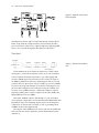
1
P E R V I C E S C O R P O R AT I O N
CRIMSON USER MANUAL
2
per vices corporation
Change Log
2014-09-01: Rev A: Initial Release
2014-09-15: Rev B: Additional specification information, system
architecture.
2014-09-18: Rev C: More information on system interfaces, initial
configuration page showing the web UI.
2014-11-04: Rev D: Added register map, data format, updated
specifications, added command guide to mem and uart-app.
2014-11-13: Rev E: Added more information on compatible NIC
cards, updated Time board architecture section.
2015-01-06: Rev F: Updating to correct IP address to manual.
2015-01-12: Rev G: Added SFP+ configuration information.
2015-01-15: Rev H: Updated register map.
2015-01-23: Rev I: Updated IP addresses.
2015-03-03: Rev J: Moved + updated specification table about,
added Crimson Update Chapter.
2015-03-04: Rev K: Added RF chain latency information, pending
more information on DSP timings.
2015-05-14: Rev L: Including network flashing instructions, installation of Per Vices libUHD driver.
Contents
Preface
5
Obligatory Warnings
7
Specifications and Interfaces
System Architecture
Installation
11
17
21
Use and Operation
29
Crimson Device Data Format
Crimson Register Map
Updating Crimson
Last Chapter
57
47
33
35
Preface
Crimson
Crimson is a high performance, wide band, high gain, direct conversion quadrature software defined radio transceiver and signal
processing platform. It has four channels, each comprised of independent receive and transmit blocks, capable of processing up to
322MHz of instantaneous RF bandwidth from DC to 6GHz and synchronized using a JESD204B subclass 1 link to ensure deterministic
latency. Data may be processed on the device itself (we have an Altera Arria V ST FPGA SoC on-board), or sent over low latency dual
10GB Ethernet links by connecting the integrated SFP+ headers to a
compatible 10GBASE-R network device.
Crimson is intended for advanced signal processing and data
collection applications.
Congratulations!
Congratulations on your purchase of the Per Vices Crimson
Transceiver! This manual is intended to provide you with useful information regarding the safe operation and use of your new
Transceiver. Although it may be updated from time to time, you’ll
always be able to find the latest version on the Per Vices website1 .
In building Crimson, we aimed to provide advanced capabilities at the lowest possible price. This product aims to provide a
sophisticated platform capable of advanced RF Signal processing and
includes a robust, and fully integrated, RF chain.
Our hope is that you will find Crimson to be a useful and dependable companion in your engineering, development, and research
efforts.
We welcome your feedback; please feel free to contact us at:
[email protected]
1
http://www.pervices.com
Obligatory Warnings
The following section contains important safety and regulatory information. Please pay attention to the following disclaimers, warnings,
and cautions.
This device is intended for engineering, research, or science laboratory use
only - it is not for open office or residential use!
Disclaimer
This product is provided «As Is». Per Vices is under no obligation
to provide updates, upgrades, support, or maintenance of any kind.
Per Vices specifically disclaims any and all warranties and guarantees, express, implied or otherwise, arising with respect to the use
of this product including, but not limited, to the warranty of merchantability, the warranty of fitness for a particular purpose, and any
warranty of non-infringement of the intellectual property rights of
any third party. Per Vices neither assumes or authorizes any person
to assume for it any other liability.
Your use of this device is at your own risk. Per Vices shall not be
liable for you or any damages, direct or indirect, incurred or arising
from the use of this product. In no event will Per Vices be liable
for loss of profits, loss of use, loss of data, business interruption,
nor for punitive, incidental, consequential, or special damages of
any kind, however caused, and on any theory of liability, whether
in contract, strict liability, or tort (including negligence or otherwise),
arising in any way out of the use of this product, even if advised of
the possibility of such damages.
Product Functionality
Every effort has been made to ensure that the device you receive is
fully functional - each device is fully tested prior to shipping. However, risk of damage or loss is transferred immediately upon delivery
to you - we do not generally accept returns or refunds on successfully delivered packages. That being said, we do want to ensure your
This device has not been tested or approved by any agency or approvals
body for Electrical Safety, Electromagnetic Compatibility, or Telecommunications at the time of distribution! You
use this device at your own risk.
8
per vices corporation
experience with Per Vices and Crimson is a pleasant one and we encourage you to contact us at [email protected] if you have
any problems.
Specifications
Every effort has been made to test and measure the validity of this
equipment. However, we cannot guarantee the accuracy of specifications, and they may change at any time.
Warnings
crimson user manual
WARNING
RISK OF ELECTRIC SHOCK
Do not attempt to modify or touch this device while powered.
Ensure host computer is properly grounded during operation.
Disconnect AC power during installing or removal.
WARNING
HOT SURFACE
This circuit board may become very hot during operation.
Contact should be avoided.
WARNING
LABORATORY USE ONLY
This device has not been approved by any agency or approvals
body for Electrical Safety, Electromagnetic Compatibility, or
Telecommunications at the time of distribution. Research use only!
ATTENTION
OBSERVE ESD PRECAUTIONS
This device contains electrostatically sensitive components: it
may be damaged by static discharges. Observe ESD precautions &
proper grounding when handling, installing, or removing device.
ATTENTION
RF TRANSMITTER
This device is capable of RF transmission on bands or frequencies
subject to regulatory oversight. Operators are responsible to ensure
use of this device meets local regulatory and legal standards, as
they may apply to you and the band of interest.
This device is intended for test and measurement use only.
9
Specifications and Interfaces
Crimson is a wide band, high gain, direct conversion quadrature
transceiver and signal processing platform. Using analogue and
digital conversion, it is capable of processing signal bandwidths up to
322MHz from approximately DC to 6GHz. Crimson is compatible
with GnuRadio, and includes source code for many of its drivers and
peripherals.
As Crimson is capable of Digital
Down/Up Conversion, superhet architectures can be implemented using
Digital Down/Up Conversion on the
FPGA.
Absolute Maximum Ratings
Stresses beyond those listed in table 1, Absolute Ratings, may cause
permanent damage to the device. These ratings are stress specifications only; functional operation of the product at these conditions
is not implied - exposure to absolute maximum rating conditions
for extended periods of time may affect reliability and is not recommended.
Specification
min
max
units
Operating Temperature
Storage Temperature
Input RF Power
5
0
85
70
15
C
C
dBm
Observed Performance
Crimson is a very flexible radio and signal processing platform that
supports high bandwith communications over a wide tuning range.
The hardware and signal processing capabilities may be configured
to support a very wide variety of applications, each with their own
figures of merit. It is therefore fairly challenging to provide uniform
performance specifications across those different configurations.
To provide a general idea of what this product is capable of, table 2 on page 15 provides some conservative figures of the out-of-box
performance of this product. Configuration of the product towards a
specific application may see you exceed some of these figures at the
Table 1: Absolute Ratings: Exposure or sustained operation
at absolute ratings may permanently damage Crimson.
Ensure fan intake vents (located
on both sides of the device) are
not blocked during operation.
12
per vices corporation
expense of others. For more information, please don’t hesitate to contact us.
External Interfaces
Crimson has a number of user accessible external interfaces through
which the device can connect to external sources and sinks. Speaking broadly, management functions are generally carried out over a
web page, hosted by the Crimson transceiver, and accessible using the management Ethernet port on the front face of the device,
and data is sent over the 10Gbps SFP+ ports. Receive and transmit
antennas connect to the SMA connectors on the front of the device.
Other peripherals ports provide access or the capability to improve
functionality.
10/100 Management Port This connects to a Linux system that is
running on the Hard Processing System located on the
FPGA silicon, and provides a unified interface by which
to control and configure the remaining devices.
10GBASE-R SFP+ There are two SFP+ ports on the front panel of the
device that use 10GBASE-R encoding to directly communicate with an optical module and interface with a ten
gigabit network. These ports directly interface with the
FPGA fabric and support high bandwidth, low latency,
communication between the ADCs and DACs.
50Ω SMA There are a number of standard SMA headers, which are
used to connect to external antennas, sinks, or sources,
including:
Rx
The four independent receive channels may be
connected to an external source or antenna
Tx
The four independent transmit channels may
be connected to external antennas or sinks
Ext. Ref
An external 10MHz reference may be applied
to this port in lieu of the default, internal,
10MHz reference
Ext. Sync An external sync may be applied to this port
to synchronize the time keeping across multiple devices, using the features provided in the
LMK04828 chip
Ext. VCO For the most demanding applications, an external VCO may be used to drive the LMK04828
It is important to note that not all
10Gbps NICs support 10GBASE-R
protocols - it’s important that you
ensure the card you select supports
communication using 10GBASE-R. If
you have questions about this, please
don’t hesitate to ask us!
crimson user manual
13
outputs. This implies a completely external
synchronization solution
USB 2.0
A USB port is provided that connects to the Linux system
running on the Hard Processor System.
Micro-SD slot The FPGA and Hard Processor System may be rebooted or configured using an external Micro-SD card.
Mini-SIM slot A Mini-SIM card may be connected, with its contacts
directly interfacing to the FPGA fabric.
ICE320 Power A standard «computer» cable plugs into this power to
power the unit. The power supply accepts 120V or 240V.
Operating System
Crimson may be used with any operating system. After physically
connecting the Crimson Transceiver to an external network or computer using its dedicated Ethernet management port, you may configure the device using the provided web interface. It is also possible
to SSH into the small Linux distribution running on the processor onboard.
Network Interface Card (NIC) Requirements
Crimson uses a 10-gigabit Ethernet connection to quickly send and
receive data. The Crimson uses a 10GBASE-R PHY that interfaces
with the SFP+ port using a single, 10.3125Gbps serial lane and a
scrambled 64B/66B coding scheme. It is very important to ensure
that network devices or interfaces intended to be used to connect
to Crimson support 10GBASE-R. The 10GBASE-R family includes
10GBASE-KR, 10GBASE-SR, 10GBASE-LR, and 10GBASE-ER interfaces.
Note that Crimson also requires active cabling: using passive, direct connect, SFP+ cables is not supported. We recommend using
active optical cabling (AOC) with integrated SFP+ transceivers. Alternatively, you may also choose to use a fibre cable and a compatible
10GBASE-R SFP+ optical transceiver module.
If you have any questions or concerns about NIC card requirements, please do not hesitate to contact us!
Mechanical
Crimson conforms to a 1U form factor and 19-inch+ rack. A mechanical drawing in included in the Appendix.
There is a significant difference
between a 10GBASE-X interface (4 serial lanes specified
to 3.125Gbps using 8b/10b
coding), and the 10GBASE-R
interface (1 serial lanes specified to 10.3125Gbps using
64b/66b coding) that Crimson
uses. Although both standards
may expose the same mechanical SFP+ interface (and thereby
allowing you to mechanically
connect the two interfaces)
the standards are fundamentally incompatible. Connecting
Crimson (10GBASE-R) to a network card that only supports
10GBASE-X or 10GBASE-T will
not work.
14
per vices corporation
RF Chain
Simulated RF chain performance, based on component specifications,
yield the simulated performance indicated in table 3 on page 16.
As both the receive and transmission chains use variable stages the
figures were calculated using midpoint references for attenuation and
gain stages - with proper tuning and calibration, you should expect
better values. More information on the specific RF chain used may be
found in the System Architecture chapter on page 17.
crimson user manual
Specification
min
Temperature
Operating Temperature
RF Tuning (HMC833)
Dyn. Range
SFDR
nom
max
Common Radio
25
10
units
C
60
6000
70
65
MHz
dB
dB
Receive Radio
RF Input Power
Noise Figure
-20
3.5
-4.5
-15
11
65
55
dBm
dB
dB
dB
ns
ns
Low
High
Low
13.7
Group Delay (Radio Chain)
High
16
ADC (Receive Converter)
Independent Channels
4
ADC resolution
16
bits
ADC Sample Rate
322.265625
MSPS
Rx Sampling Bandwidth
322.265625
MHz
Latency (input to serial)
50
ns
Receive DSP and FPGA Specifications (Default firmware)
Power Gain
f
Decimation ( ns )
Latency (FPGA DSP)
1
256
102
180
Transmit Radio
Low
-10
20
Transmit Power
High
Low
4.3
Group Delay (radio chain)
High
8.9
DAC (Transmit Converter)
Tx Output Bandwidth
322.265625
DAC resolution
16
DAC Sample Rate
322.265625
Latency (serial to output)
50
655
804
Transmit DSP and FPGA Specifications
Interpolation (n · f s )
1
256
Latency (FPGA DSP)
96
174
Digital
FPGA - Arria V ST SOC
5ASTMD3E3F31
On Board Processor Core
ARM Cortex-A9 MP
LPDDR2 RAM
4
NAND Flash (x8)
4
Networking
10GBASE-R, Full Duplex
each
8
Default IP, SFP+ Port A
10.10.10.2
Default IP, SFP+ Port B
10.10.11.2
Internal Reference (10 MHz)
Frequency Calibration
-5
5
15
ns
dBm
ns
ns
MHz
bits
MSPS
ns
ns
Gb
Gb
Gbps
ppb
Table 2: Observed Performance.
These specifications reference
observations taken during internal use and development. Calibration Measurements relative
to 20o C
16
per vices corporation
Specification
Specification
Value
units
Input Parameters
Input Power
-55
dBm
Frequency
2000 MHz
Analysis B/W
150
MHz
Value
Rx Chain Analysis
SFDR
40-55
IMD
-69
IIP3
-23.5
SNR
33.8
Rx Sensitivity
-85
Input P1dB
-43
Tx Chain Analysis
Power Gain
SFDR
units
dB
dB
dB
dB
dBm
dBm
dB
dB
Table 3: These specifications are
intended to serve as a broad
guide, with variable gain and
attenuation stages set at midpoints. As variable stages are
adjusted, performance generally improves.
System Architecture
Overview
Figure 1: Overall system block
diagram.
Crimson uses a highly modular design consisting of four boards,
each connected using shielded, high speed cabling, to support its
operation (Figure 1). The digital board provides an interface to the
control and configures the receive, transmit, and time boards, along
with high speed connections to the receive (Rx) and transmit (Tx)
boards. Clock distribution extends from the Time board, which provides a very clean and stable clock distribution network. The default
receive and transmit boards each comprise of four fully independent
channels.
Digital board
The Crimson digital board provides the digital processing that
powers the Crimson transceiver. It consists of a Altera Arria V ST
SOC FPGA, which includes an ARM Cortex-A9 processor on the
FPGA, and an Atmel ATxMega Microcontroller (Figure 2 on the next
page). The HPS portion of the board hosts the web server by which
we can configure Crimson, along with an Atmel ATxmega256A3
microcontroller, which is used to communicate with the Rx, Tx, and
time module. A separate, high speed, link allows serial data to be
18
per vices corporation
Figure 2: Digital board system
block diagram.
shared between the Rx and Tx boards and directly with the FPGA
fabric, along with the 10Gbps interface (accessed using the SFP+
ports on the front of the device). Other peripherals, including USB
devices, are accessed through the HPS portion of the FPGA.
Time Board
Figure 3: Time Board Architecture
Clock distribution on the Crimson transceiver is fairly robust
(See Figure 3). Our internal reference source is an oven-controlled
crystal oscillator (OCXO) that provides a very stable (5ppb) and
accurate 10MHz signal. The reference clock is used as an input to
the HMC1031MS8 Clock Generator with integer-N PLL to lock our
external, ultra-low phase noise Crystec CVHD-950-100.000 100MHz
TCVXO to the long term stability of our OCXO. This improves output clock jitter and phase noise while preserving the stability and
accuracy of our 10MHz reference - ultimately leading to superior
frequency stability, data convertor signal-to-noise ratio (SNR), and
digital PHY bit-error rates (BER).
This stable 100MHz output is fed through a 1:9 fan out buffer,
whose primary output drives a Texas Instruments LMK04828B Clock
Distribution chip. The remaining outputs are fed to the frequency
synthesizers on the Rx and Tx boards, as well as providing clean,
100MHz clocks for the digital board.
The outputs of the LMK04828 are used to generate the JESD204B
device and system clocks required to ensure deterministic latency
(subclass 1).
crimson user manual
19
Receive Board Radio Chain
BFP843
High Stage
High Stage LNA
A
1
A
1
2
TQP369180
3
SKY13351-378LF
RF Gain
ADL5380
A
2
I
1
3
Q
SKY13351-378LF
IQ Downconverter
Figure 4: Rx Board RF Channel
I
Q
2
2
BB03
Q 2
3
RX Antenna SKY13351-378LF
(50 Ohm)
Frequency Synthesizer
AG403-89G
BB13
A
1
HMC922LP4
A
1
HMC922LP4
ADRF6518
ADC16DX370
FPGA
5ASTMD3E
ADC Driver + Filter ADC
Low Stage
Varactor Circuit (Group Delay)
Amplifier
The Crimson receive board consists of a radio front end terminating with the Texas Instruments dual channel ADC16DX370 analog-todigital converter, as shown in Figure 4. This architecture is duplicated
four times, once for each channel.
Transmit Board Radio Chain
Figure 5: Tx Board RF Channel
The Crimson transmit board consists of a radio front end originating with the Texas Instruments quad channel DAC38J84 digital-toanalog converter, as shown in Figure 5. The radio front end is duplicated four times, but with channels A and B connecting to one DAC,
and channels C and D connecting to another DAC.
Installation
Installation comprises of two parts; physically installing the unit
(attaching antennas, cables, power), configuring the network on your
host computer, and building and installing the Per Vices libUHD
library.
Physical Installation
Physical installation comprises of three steps;
1. Attaching the antennas to the Transmit and Receive ports labeled
RXA - RXD for the receive and TXA - TXD for the transmit.
2. Physically connecting an RJ-45 cable from the Management port
on Crimson to the client computer, and then connecting the
10GBASE-R cables to the host computer.
3. Connecting the power plug of the Crimson unit, and turning on
the unit.
Default Crimson Network Configuration
Crimson boasts three network ports. The Management port is used
to configure the device, while data is sent over the two SFP+ ports.
Each SFP+ data port is connected to a specific antenna port. The default configuration has data on channels A and C sent over SFP+ A,
and channels B and D sent over SFP+ B, as illustrated in Figure 6 on
the next page. The default network values are listed in Table 4 on the
following page, while the default recommended client networking
configuration is on Table 5 on the next page.
22
per vices corporation
Figure 6: Default networking
set up for Crimson. The destination IP addresses for receive
ports may be modified using the web GUI. The default
configuration sees information
from Rx A sent to the destination IP address of 10.10.10.
Crimson IP Address
Radio Channels
Destination IP (Rx)
Rx UDP Ports
Source IP (Tx)
Tx UDP Ports
Host Address
Net Mask
Broadcast
MTU
SFP+ Interface
Port A
Port B
10.10.10.2
10.10.11.2
AC
BD
10.10.10.10
10.10.11.10
42820, 42822 42821, 42823
any
any
42824, 42826 42825,42827
SFP+ Interface
Port A
Port B
10.10.10.10
10.10.11.10
255.255.255.0 255.255.255.0
10.10.10.255
10.10.11.255
9000
9000
Management
Mgmt
192.168.10.2
-
Management
Mgmt
192.168.10.4
255.255.255.0
192.168.10.255
1500
Table 4: Default Crimson Interface Addresses, including
UDP destination ports for SFP+
headers.
Table 5: Host computer network configuration used in
Figure <>, and used in default
configuration.
crimson user manual
23
Configuring Your IP Address to access the Management Site
In order to access the web interface, you shall need to configure your
IP address to share the same sub net (setting your machine to an IP
of 192.168.10.4, and net mask of 255.255.255.0 should work), and then
type the IP address into the browser; 192.168.10.2. This should bring
up the default connection screen for Crimson (shown in Figure 7).
Figure 7: Home page of Crimson Web UI, accessible through
connection to the management
port.
You can reconfigure the IP address, and host name, by clicking on
the «Debug» tab of the home page.
You can also SSH into Crimson with user name root and by
default there is no password set up.
Arch Linux
You can assign a static IP address in the console:
# ip addr add XXX.XXX.XXX.XXX/YY broadcast ZZZ.ZZZ.ZZZ.ZZZ
dev interface
For example:
# ip addr add 192.168.10.3 broadcast 192.168.10.255 dev eth0
Debian/Ubuntu/Kubuntu
Log in as root and open a terminal
Make a backup of your /etc/network/interfaces file by typing the
following in the console:
cp /etc/network/interfaces /etc/network/interfaces.backup
Then open vi by typing:
vi /etc/network/interfaces
24
per vices corporation
Press «i» to enter into insert (editing) mode, and scroll down until
you find your network interface card in the file. This usually starts
with ethX for a wired network card (wireless cards generall start
with wlanX or wifiX). This line generally holds a default value of
«dhcp», which you need to replace with «static», after which you
add the appropriate address, netmask, and network parameters. See
table 6 for a specific example that illustrates the change that needs to
be made. Once you have made the appropriate change, you can type
«:wq» from within vi to save (write) your changes to the file and exit.
After making your changes, you may need to cycle your internet
adapter. You may do this by typing the following command:
ifdown eth0; ifup eth0
Note: if you are remotely logged into the machine, it’s possible this
may bring down the network adapter you are using - therefore, ensure
you have correctly identified your adapter prior to making this change.
Old
New
<...>
iface eth0 inet dhcp
<...>
<...>
iface eth0 inet static
address 192.168.10.3 netmask 255.255.255.0 network 192.168.10.3
<...>
Windows (generic)
The following describes the generic method of changing your IP
address using a Windows machine.
Go to Control Panel
View Network Connections
Right click on Local Area Connection and click on Properties
Under the Networking tab select Internet Protocol Version 4
(TCP/IPv4) and click on Properties
Select «Use the following IP address»
Populate the IP address and subnet mask as described above
Click OK
Configuring Your Data SFP+ IP Addresses
Assuming that the 10GBASE-R network card has already been installed into your host computer, the following instructions will guide
you in properly configuring the SFP+ ports. From here, we will assume that the SFP+ port A is named XXXNXY. The IP address for
this port will need to be configured to 10.10.10.10.
Table 6: Sample line replacement within /etc/network/interfaces
crimson user manual
Arch Linux
You can assign a static IP address in the console:
# ip addr add XXX.XXX.XXX.XXX/YY broadcast ZZZ.ZZZ.ZZZ.ZZZ
dev interface
For example, referencing Table 5 on page 22;
# ip addr add 10.10.10.10/24 broadcast 255.255.255.0 dev XXXNXY
Type «ip addr show» into the console and the following output
should appear to indicate that the link is up:
5: XXXNXY: <BROADCAST,MULTICAST,UP,LOWER_UP> mtu 9000
qdisc mq state UP group default qlen 1000 link/ether NN:NN:NN:NN:NN:NN
brd ff:ff:ff:ff:ff:ff
You can now ping the SFP+ Port A address 10.10.10.2 to ensure
proper operation by typing the following into the console:
# ping -I XXXNXY 10.10.10.2
PING 10.10.10.2 (10.10.10.2) from 10.10.10.10 XXXNXY: 56(84) bytes of
data.
64 bytes from 10.10.10.2: icmp_seq=1 ttl=5 time=0.922 ms
64 bytes from 10.10.10.2: icmp_seq=2 ttl=5 time=1.03 ms
...
In the event that 10.10.10.2 is not responding, you can type the following command into the console to check which IP address the port
is linked to (shown as XX.XX.XX.XX):
# ping -I XXXNXY -b 255.255.255.255
WARNING: pinging broadcast address
PING 255.255.255.255 (255.255.255.255) from 10.10.10.10 XXXNXY:
56(84) bytes of data.
64 bytes from XX.XX.XX.XX: icmp_seq=1 ttl=5 time=0.759 ms
64 bytes from XX.XX.XX.XX: icmp_seq=2 ttl=5 time=0.846 ms
...
To configure SFP+ Port B, repeat the above instructions but replace IP
addresses as shown in Table 5 on page 22.
Debian/Ubuntu/Kubuntu
Log in as root and open a terminal
Make a backup of your /etc/network/interfaces file by typing the
following in the console:
cp /etc/network/interfaces /etc/network/interfaces.backup
25
26
per vices corporation
Then open vi by typing:
vi /etc/network/interfaces
Press «i» to enter into insert (editing) mode, and scroll down until
you find your network interface card in the file. This line generally holds a default value of «dhcp», which you need to replace with
«static», after which you add the appropriate address, netmask, and
network parameters. See table 7 for a specific example that illustrates
the change that needs to be made. Once you have made the appropriate change, you can type «:wq» from within vi to save (write) your
changes to the file and exit.
After making your changes, you may need to cycle your internet
adapter. You may do this by typing the following command:
ifdown XXXNXY; ifup XXXNXY
Note: if you are remotely logged into the machine, it’s possible this
may bring down the network adapter you are using - therefore, ensure
you have correctly identified your adapter prior to making this change.
Old
New
<...>
iface XXXNXY inet dhcp
<...>
<...>
iface XXXNXY inet static
address 10.10.10.10 netmask 255.255.255.0 network 10.10.10.10
<...>
To configure SFP+ Port B, repeat the above instructions but replace
IP addresses as shown in 5 on page 22.
Windows (generic)
Please refer to the previous Windows (generic) IP address configuration section.
Building the UHD Drivers
To fully realize the potential of Crimson, you’ll need to build and
install the UHD drivers. To do this, you will have compile the Per
Vices libUHD sources.
Obtaining the Per Vices UHD Sources
You may easily download the Per Vices UHD sources from github.
From the command line;
$ git clone https://github.com/pervices/uhd.git
Table 7: Sample line replacement within /etc/network/interfaces
crimson user manual
Download the dependencies
Once you have downloaded the Per Vices UHD repository, you may
want to confirm that you have all the dependencies required. Detailed instructions, including the dependencies are available here;
http://files.ettus.com/manual/page_build_guide.html
Note: In order to use Crimson with UHD, you must download the
Per Vices UHD version, as it contains all the required modifications
needed to support the Per Vices drivers.
Quick Install Instructions
We really recommend that you carefully read the UHD build instructions. But if you’re impatient, feeling lucky, and confident that you
have all the dependencies, here’s what you should be able to do;
#download the dependencies
$ git clone https://github.com/pervices/uhd.git
#enter the host directory
cd <uhd-repository-directory>/host
mkdir build
cd build
#run cmake with the appropriate compile flags
cmake .. -DCMAKE_INSTALL_PREFIX=/usr/ \
-DPYTHON_EXECUTABLE=/usr/bin/python2 \
-DENABLE_EXAMPLES=OFF \
-DENABLE_UTILS=ON \
-DENABLE_TESTS=OFF \
-DENABLE_E100=ON
make -j4
make install
27
Use and Operation
This device is designed to be used and configured over a dedicated
management port. The primary user interface can either be the a web
UI, or you may directly configure the device over SSH.
Web UI
You may access the web interface by typing the IP address of the
device in your browser. This directs you to a SCADA-like interface
where you can easily visualize and configure the radio chain and
DSP carried out on the device.
SSH and Command Line
You may also access and configure the device over SSH using command line parameters. This is primarly done using two programs;
«uart-app» and «mem». The uart-app programs allow you to send
commands over the UART bus to radio peripherals (like ADCs,
DACs, or Amplifiers), and the mem application allows you to read
and write to the memory space shared between the HPS and the
FPGA.
Crimson uart-app
Crimson uses a number of MCUs, located on the Rx, Tx, Synthesizer, and Digital boards, to communicate and interface with various
peripheral devices. This is done through a UART bus between the
ARM Hard Processor System on the FPGA and the Atmel MCU on
the digital board. The digital board has three other UART busses and
forwards or processes requests through to the Rx, Tx, and Synthesizer board. You can directly poll and send commands to the MCU
through the uart-app utility.
For example, to return a list of available commands on the synthesizer board, you might type;
#uart-app ”help -v”
30
per vices corporation
Board: DIG
Usage: [cmd] [-|–][arg1] [-|–][arg2]...
Commands:
fpga Commands for controlling the FPGA.
[r|rst] Resets the FPGA through the reset pin.
dsp Configure the DSP features (FPGA/SW).
[c|chan] Specify which channel a,b,c,d OR bit mask. MUST specify first.
[s|stage] Enable the interpolator/decimator stage (1 - 5). SHOULD
specify second.
[h|chain] Specify which chain ADC(1), DAC(0). SHOULD specify
third.
[e|en] Enable(1) disable(0) the stage.
[f|freq] Specify the frequency of the NCO.
fwd Forward messages to the other boards.
[b|board] Forward to RX(0), TX(1), SYNTH(2), echo(3).
[m|msg] Forward message, max 25 chars.
switch Switches the UART communication to another board.
[t|tx] Switches to the TX board.
[r|rx] Switches to the RX board.
[s|synth] Switches to the Synth board.
jesd Executes any JESD required commands.
[s|sync] Re-sync all of the boards’ sysref syncs.
status Provides the status of the board.
[f|fpga] Reads the status of the FPGA.
[e|eth] Reads the status of the 10G ethernet PHY.
[r|ret] Reads the return value of the last function that was called.
[p|pwr] Reads the current enabled power rails and pgood status.
[i|i2c] Reads the status byte for the i2c register.
test Executes test vectors.
[f|fpga] Runs specified test vector of the FPGA.
crimson user manual
[e|eth] Runs specified test vector of the 10G ethernet PHY.
board Controls the board level functions. Sequential exec of arguments.
[i|init] Rewrite all regs for entire board.
[d|demo] Turn on outputs (per channel).
[e|diag] Runs diagnostic on peripheral (per channel). Should print
all registers.
[m|mute] Turn off outputs (per channel).
[r|reset] Power cycle peripherals and runs board init (per channel).
[k|kill] Turn off peripherals. [p|panic] Turns everything off.
[v|version] Prints out the software and hardware version.
[l|led] Blinks the LED a specified number of times.
[t|temp] Provides the temperature (0-1).
[a|ram] Provides the amount of RAM left (bytes).
boot Bootloader options.
[e|enter] Enter the boot loader.
exit Doesn’t do anything, place holder.
[-|–] No argument necessary.
help Prints out the help menu for the board.
[v|verbose] Prints out in verbose mode. 1 to enable.
Switching to a different board, and typing the ”help -v” operator provides you with board specific commands and configuration utilities
for the respective peripherals.
Crimson mem
If you choose to directly interface with the device over SSH, the mem
tool is a helpful utility that allows you to read and write registers
from the command line. The mem tool supports the following options:
mem [mr|mw|md|rr|rw|rd|rl] [address|reg_name|verbosity]
[value|length]
Where,
mr memory read
31
32
per vices corporation
mw memory write
md memory
rr raw read
rw raw write
rd read double
rl read long
address the memory address in question
reg_name the register memomic (as defined in the Crimson Register
Map).
value hex value to write
length length (in bytes) of a read
Crimson Device Data Format
Crimson uses complex, signed, 32-bit integers to communicate data
over the SFP+ ports.
Data Format
Data are transmitted in IQ pairs. Each IQ pair is 32 bits, with the I
and Q components represented by two 16 bit signed integers. The
specific format is represented in Table 8. To read this data inside
GNU radio, you can use a flow chart similar to that shown in Figure 8.
Bit Position
31:24
23:16
15:8
7:0
Representation
Re[7:0]
Re[15:8]
Im[7:0]
Im[15:8]
Table 8: Data structure
Figure 8: Sample gnuradio data
sink, visualizing waterfall data.
Crimson Register Map
The following pages detail the Crimson registermap. This is used to
configure various paramers on the FPGA, and includes 10Gbps backhaul, and JESD204B parameters between the FPGA and converter
devices.
Channel
System
SFP+A
Network
SFP+B
A
B
RX
C
D
A
B
TX
C
D
Reserved
Channel
Register
sys0
sys1
sys2
net0
net1
net2
net3
net4
net5
net6
net7
net8
net9
net10
net11
net12
net13
net14
net15
net16
net17
net18
net19
net20
net21
net22
net23
net24
net25
net26
net27
net28
net29
Address
0x0000
0x0010
0x0020
0x0200
0x0210
0x0220
0x0230
0x0240
0x0250
0x0260
0x0270
0x0280
0x0290
0x02a0
0x02b0
0x02c0
0x02d0
0x02e0
0x02f0
0x0300
0x0310
0x0320
0x0330
0x0340
0x0350
0x0360
0x0370
0x0380
0x0390
0x03a0
0x03b0
0x03c0
0x03d0
Default
Bit 31
0x00000000
0xffff003f
0x00000000
0x05780002
0x00000000
0x00000000
0x00000000
0x00000000
0x0a0a0a02
0x00000000
0x00000000
0x00000000
0x00000000
0x00000000
0x0000aa00
0x00000000
0x00007a69
0x00000000
0x05780002
0x00000000
0x00000000
0x00000000
0x00000000
0x0a0a0b02
0x00000000
0x00000000
0x00000000
0x00000000
0x00000000
0x0000aa00
0x00000001
0x00007a6a
0x00000000
rxa0
rxa1
rxa2
rxa3
rxa4
rxa5
rxa6
rxa7
rxa8
0x0400
0x0410
0x0420
0x0430
0x0440
0x0450
0x0460
0x0470
0x0480
0x00000000
0x000000ff
0x00000000
0x00000000
0x00000000
0x0a0a0a0a
0x0000ffff
0xffffffff
0x0000a744
rxb0
rxb1
rxb2
rxb3
rxb4
rxb5
rxb6
rxb7
rxb8
0x0500
0x0510
0x0520
0x0530
0x0540
0x0550
0x0560
0x0570
0x0580
0x00000000
0x000000ff
0x00000000
0x00000000
0x00000200
0x0a0a0b0a
0x0000ffff
0xffffffff
0x0000a745
rxc0
rxc1
rxc2
rxc3
rxc4
rxc5
rxc6
rxc7
rxc8
0x0600
0x0610
0x0620
0x0630
0x0640
0x0650
0x0660
0x0670
0x0680
0x00000000
0x000000ff
0x00000000
0x00000000
0x00000000
0x0a0a0a0a
0x0000ffff
0xffffffff
0x0000a746
rxd0
rxd1
rxd2
rxd3
rxd4
rxd5
rxd6
rxd7
rxd8
0x0700
0x0710
0x0720
0x0730
0x0740
0x0750
0x0760
0x0770
0x0780
0x00000000
0x000000ff
0x00000000
0x00000000
0x00000200
0x0a0a0b0a
0x0000ffff
0xffffffff
0x0000a747
txa0
txa1
txa2
txa3
txa4
txa5
0x0800
0x0810
0x0820
0x0830
0x0840
0x0850
0x00000000
0x000000ff
0x00000000
0x00000000
0x00000000
0x0000a748
txb0
txb1
txb2
txb3
txb4
txb5
0x0900
0x0910
0x0920
0x0930
0x0940
0x0950
0x00000000
0x000000ff
0x00000000
0x00000000
0x00000200
0x0000a749
txc0
txc1
txc2
txc3
txc4
txc5
0x0a00
0x0a10
0x0a20
0x0a30
0x0a40
0x0a50
0x00000000
0x000000ff
0x00000000
0x00000000
0x00000000
0x0000a74a
txd0
txd1
txd2
txd3
txd4
txd5
0x0b00
0x0b10
0x0b20
0x0b30
0x0b40
0x0b50
0x00000000
0x000000ff
0x00000000
0x00000000
0x00000200
0x0000a74b
rsvd0
rsvd1
rsvd2
rsvd3
rsvd4
rsvd5
rsvd6
rsvd7
rsvd8
rsvd9
rsvd10
rsvd11
rsvd12
rsvd13
rsvd14
rsvd15
0x0f00
0x0f10
0x0f20
0x0f30
0x0f40
0x0f50
0x0f60
0x0f70
0x0f80
0x0f90
0x0fa0
0x0fb0
0x0fc0
0x0fd0
0x0fe0
0x0ff0
0x00000000
0x00000000
0x00000000
0x00000000
0x00000000
0x00000000
0x00000002
0x00000000
0x00000000
0x00000000
0x00000000
0x00000000
0x00000000
0x00000000
0x00000000
0x00000000
Register
Address
Default
30
29
28
27
26
25
24
23
22
21
20
19
18
17
16
15 14
13
reserved[31:4]
rtx_rdy[31:16]
12
11
10
9
8
7
6
5
4
3
Address
0x0000
0x0010
0x0020
0x0200
0x0210
0x0220
0x0230
0x0240
0x0250
0x0260
0x0270
0x0280
0x0290
0x02a0
0x02b0
0x02c0
0x02d0
0x02e0
0x02f0
0x0300
0x0310
0x0320
0x0330
0x0340
0x0350
0x0360
0x0370
0x0380
0x0390
0x03a0
0x03b0
0x03c0
0x03d0
Register
sys0
sys1
sys2
net0
net1
net2
net3
net4
net5
net6
net7
net8
net9
net10
net11
net12
net13
net14
net15
net16
net17
net18
net19
net20
net21
net22
net23
net24
net25
net26
net27
net28
net29
conv end rst_dsp rst_pkr
0x0400
0x0410
0x0420
0x0430
0x0440
0x0450
0x0460
0x0470
0x0480
rxa0
rxa1
rxa2
rxa3
rxa4
rxa5
rxa6
rxa7
rxa8
conv end rst_dsp rst_pkr
0x0500
0x0510
0x0520
0x0530
0x0540
0x0550
0x0560
0x0570
0x0580
rxb0
rxb1
rxb2
rxb3
rxb4
rxb5
rxb6
rxb7
rxb8
conv end rst_dsp rst_pkr
0x0600
0x0610
0x0620
0x0630
0x0640
0x0650
0x0660
0x0670
0x0680
rxc0
rxc1
rxc2
rxc3
rxc4
rxc5
rxc6
rxc7
rxc8
conv end rst_dsp rst_pkr
0x0700
0x0710
0x0720
0x0730
0x0740
0x0750
0x0760
0x0770
0x0780
rxd0
rxd1
rxd2
rxd3
rxd4
rxd5
rxd6
rxd7
rxd8
0x0800
0x0810
0x0820
0x0830
0x0840
0x0850
txa0
txa1
txa2
txa3
txa4
txa5
0x0900
0x0910
0x0920
0x0930
0x0940
0x0950
txb0
txb1
txb2
txb3
txb4
txb5
0x0a00
0x0a10
0x0a20
0x0a30
0x0a40
0x0a50
txc0
txc1
txc2
txc3
txc4
txc5
0x0b00
0x0b10
0x0b20
0x0b30
0x0b40
0x0b50
txd0
txd1
txd2
txd3
txd4
txd5
0x0f00
0x0f10
0x0f20
0x0f30
0x0f40
0x0f50
0x0f60
0x0f70
0x0f80
0x0f90
0x0fa0
0x0fb0
0x0fc0
0x0fd0
0x0fe0
0x0ff0
rsvd0
rsvd1
rsvd2
rsvd3
rsvd4
rsvd5
rsvd6
rsvd7
rsvd8
rsvd9
rsvd10
rsvd11
rsvd12
rsvd13
rsvd14
rsvd15
Address
Register
rst_ctrl_busy jesd_pll_lock_l jesd_pll_lock_r
reserved[15:7]
reserved[31:4]
pl_size[31:16]
reserved[15:3]
2
1
0
opr_mode[3:0]
rx_alldev_aligned[3:0]
pack_mode[3:0]
sel crc_en
rst
ipv6_src_ip_uu[31:0]
ipv6_src_ip_ul[31:0]
ipv6_src_ip_lu[31:0]
ipv6_src_ip_ll[31:0]
ipv4_src_ip[31:0]
ipv6_dest_ip_uu[31:0]
ipv6_dest_ip_ul[31:0]
ipv6_dest_ip_lu[31:0]
ipv6_dest_ip_ll[31:0]
ipv4_dest_ip[31:0]
reserved[31:16]
mac_addr_u[15:0]
mac_addr_l[31:0]
reserved[31:16]
reserved[31:16]
pl_size[31:16]
src_port[15:0]
dest_port[15:0]
reserved[15:3]
sel
crc_en
rst
ipv6_src_ip_uu[31:0]
ipv6_src_ip_ul[31:0]
ipv6_src_ip_lu[31:0]
ipv6_src_ip_ll[31:0]
ipv4_src_ip[31:0]
ipv6_dest_ip_uu[31:0]
ipv6_dest_ip_ul[31:0]
ipv6_dest_ip_lu[31:0]
ipv6_dest_ip_ll[31:0]
ipv4_dest_ip[31:0]
reserved[31:16]
mac_addr_u[15:0]
mac_addr_l[31:0]
reserved[31:16]
reserved[31:16]
src_port[15:0]
dest_port[15:0]
NOTE: Registers 0x03d1 to 0x03ff are RESERVED. Default: 0x00000000
phase_word[31:0]
reserved[31:16]
decimation[15:0]
iq_amp[31:0]
iq_phase[31:0]
revphase
dest_sink[12:9]
ipv4_dest_ip[31:0]
reserved[31:14]
enable
signd
rx_mode[7:5]
reserved[31:16]
mac_addr_u[15:0]
mac_addr_l[31:0]
reserved[31:16]
port[15:0]
NOTE: Registers 0x0481 to 0x04ff are RESERVED. Default: 0x00000000
phase_word[31:0]
reserved[31:16]
decimation[15:0]
iq_amp[31:0]
iq_phase[31:0]
revphase
dest_sink[12:9]
ipv4_dest_ip[31:0]
reserved[31:14]
enable
signd
rx_mode[7:5]
reserved[31:16]
mac_addr_u[15:0]
mac_addr_l[31:0]
reserved[31:16]
port[15:0]
NOTE: Registers 0x0581 to 0x05ff are RESERVED. Default: 0x00000000
phase_word[31:0]
reserved[31:16]
decimation[15:0]
iq_amp[31:0]
iq_phase[31:0]
revphase
dest_sink[12:9]
ipv4_dest_ip[31:0]
reserved[31:14]
enable
signd
rx_mode[7:5]
reserved[31:16]
mac_addr_u[15:0]
mac_addr_l[31:0]
reserved[31:16]
port[15:0]
NOTE: Registers 0x0681 to 0x06ff are RESERVED. Default: 0x00000000
phase_word[31:0]
reserved[31:16]
decimation[15:0]
iq_amp[31:0]
iq_phase[31:0]
revphase
dest_sink[12:9]
ipv4_dest_ip[31:0]
reserved[31:14]
enable
signd
rx_mode[7:5]
reserved[31:16]
mac_addr_u[15:0]
mac_addr_l[31:0]
reserved[31:16]
port[15:0]
NOTE: Registers 0x0781 to 0x07ff are RESERVED. Default: 0x00000000
phase_word[31:0]
reserved[31:16]
Interpolation[15:0]
iq_amp[31:0]
iq_phase[31:0]
revphase
src_sink[12:9]
reserved[31:14]
reserved[31:16]
enable
signd
tx_mode[7:5]
port[15:0]
conv end rst_dsp rst_pkr
NOTE: Registers 0x0851 to 0x08ff are RESERVED. Default: 0x00000000
phase_word[31:0]
reserved[31:16]
Interpolation[15:0]
iq_amp[31:0]
iq_phase[31:0]
revphase
src_sink[12:9]
reserved[31:14]
reserved[31:16]
enable
signd
tx_mode[7:5]
port[15:0]
conv end rst_dsp rst_pkr
NOTE: Registers 0x0951 to 0x09ff are RESERVED. Default: 0x00000000
phase_word[31:0]
reserved[31:16]
Interpolation[15:0]
iq_amp[31:0]
iq_phase[31:0]
revphase
src_sink[12:9]
reserved[31:14]
reserved[31:16]
enable
signd
tx_mode[7:5]
port[15:0]
conv end rst_dsp rst_pkr
NOTE: Registers 0x0a51 to 0x0aff are RESERVED. Default: 0x00000000
phase_word[31:0]
reserved[31:16]
Interpolation[15:0]
iq_amp[31:0]
iq_phase[31:0]
revphase
src_sink[12:9]
reserved[31:14]
reserved[31:16]
Bit 31
30
29
28
27
26
25
24
23
22
21
20
enable
NOTE: Registers 0x0b51 to 0x0eff are RESERVED. Default: 0x00000000
reserved[31:0]
reserved[31:0]
reserved[31:0]
reserved[31:0]
reserved[31:0]
reserved[31:0]
reserved[31:0]
reserved[31:0]
reserved[31:0]
reserved[31:0]
reserved[31:0]
reserved[31:0]
reserved[31:0]
reserved[31:0]
reserved[31:0]
reserved[31:0]
NOTE: Registers 0x0ff1 to 0x0fff are RESERVED. Default: 0x00000000
19 18
17 16
15 14
13
12 11
10
9
8
signd
tx_mode[7:5]
port[15:0]
7
6
5
4
conv end rst_dsp rst_pkr
3
2
1
0
sys0 (0x0000) - System Register, Default: 0x00000000
Register Name
Address (Hex)
Bit
Name
31:4
reserved
sys0
0x0000
3:0
opr_mode
Function
Reserved
Operation mode of the system:
0000: Normal Operation
0001: Loopback. This mode will route RXn->TXn bypassing DSP engine
0010: Reserved
...
1110: Reserved
1111: Set System Reset (Enable system reset)
Default
0x0
0x0
Access
RW
RW
Default
0xffff
Access
RO
0x0
0x0
0x1
0x1
0xf
RO
RO
RO
RO
RO
Function
Reserved
Specifies the data packing order for SFP+. Each data packet will consist of 64’b which is equivalent to four 16’b samples.
The supported modes are:
0000: Reserved
0001: [A0A1A2A3]
0010: [B0B1 B2 B3]
0011: [A0B0A1B 1]
0100: [C0C 1C2C3]
0101: [A0C0A1C1]
0110: [B0C0B 1C 1]
0111: Reserved
1000: [D0D1D2D3 ]
1001: [A0D0 A1 D1]
1010: [B0D0 B1D1]
1011: Reserved
1100: [C0D0C 1 D1]
1101: Reserved
...
1110: Reserved
1111: [A0B0C 0D0]
Default
0x0
0x0
Access
RW
RW
Function
Payload size for SFPA.
Reserved
IP Protocol
0: IPV4
1: IPV6
CRC Enable
0: Disable
1: Enable
Active HIGH Reset. SFPA block will be placed in reset.
Default
0x0578
0x0
0x0
Access
RW
RW
RW
0x1
RW
0x0
RW
net1 (0x0210) – SFP+ A Register, Default: 0x00000000
Register Name
Address (Hex)
Bit
Name
net1
0x0210
31:0
ipv6_src_ip_uu
Function
Most significant 32'b of IPV6 Crimson address.
Default
0x0
Access
RW
net2 (0x0220) – SFP+ A Register, Default: 0x00000000
Register Name
Address (Hex)
Bit
Name
net2
0x0220
31:0
ipv6_src_ip_ul
Function
2nd most significant 32'b of IPV6 Crimson address.
Default
0x0
Access
RW
net3 (0x0230) – SFP+ A Register, Default: 0x00000000
Register Name
Address (Hex)
Bit
Name
net3
0x0230
31:0
ipv6_src_ip_lu
Function
2nd least significant 32'b of IPV6 Crimson address.
Default
0x0
Access
RW
net4 (0x0240) – SFP+ A Register, Default: 0x00000000
Register Name
Address (Hex)
Bit
Name
net4
0x0240
31:0
ipv6_src_ip_ll
Function
Least significant 32'b of IPV6 Crimson address.
Default
0x0
Access
RW
net5 (0x0250) – SFP+ A Register, Default: 0x0a0a0a02
Register Name
Address (Hex)
Bit
Name
net5
0x0250
31:0
ipv4_src_ip
Function
IPV4 Crimson address.
Default
0x0a0a0a02
Access
RW
net6 (0x0260) – SFP+ A Register, Default: 0x00000000
Register Name
Address (Hex)
Bit
Name
net6
0x0260
31:0
ipv6_dest_ip_uu
Function
Most significant 32'b of IPV6 destination address. (Deprecated)
Default
0x0
Access
RW
net7 (0x0270) – SFP+ A Register, Default: 0x00000000
Register Name
Address (Hex)
Bit
Name
net7
0x0270
31:0
ipv6_dest_ip_ul
Function
2nd most significant 32'b of IPV6 destination address. (Deprecated)
Default
0x0
Access
RW
net8 (0x0280) – SFP+ A Register, Default: 0x00000000
Register Name
Address (Hex)
Bit
Name
net8
0x0280
31:0
ipv6_dest_ip_lu
Function
2nd least significant 32'b of IPV6 destination address. (Deprecated)
Default
0x0
Access
RW
net9 (0x0290) – SFP+ A Register, Default: 0x00000000
Register Name
Address (Hex)
Bit
Name
net9
0x0290
31:0
ipv6_dest_ip_ll
Function
Least significant 32'b of IPV6 destination address. (Deprecated)
Default
0x0
Access
RW
net10 (0x02a0) – SFP+ A Register, Default: 0x00000000
Register Name
Address (Hex)
Bit
Name
net10
0x02a0
31:0
ipv4_dest_ip
Function
IPV4 destination address. (Deprecated)
Default
0x0
Access
RW
net11 (0x02b0) – SFP+ A Register, Default: 0x0000aa00
Register Name
Address (Hex)
Bit
Name
31:16
reserved
net11
0x02b0
15:0
mac_addr_u
Function
Reserved
Most significant 16'b of Crimson MAC address
Default
0x0
0xaa00
Access
RW
RW
net12 (0x02c0) – SFP+ A Register, Default: 0x00000000
Register Name
Address (Hex)
Bit
Name
31:0
mac_addr_l
net12
0x02c0
Function
Lower 32'b of Crimson MAC address
Default
0x00000000
Access
RW
net13 (0x02d0) – SFP+ A Register, Default: 0x00007a69
Register Name
Address (Hex)
Bit
Name
31:16
reserved
net13
0x02d0
15:0
src_port
Function
Reserved
UDP source port
Default
0x0
0x7a69
Access
RW
RW
net14 (0x02e0) – SFP+ A Register, Default: 0x00000000
Register Name
Address (Hex)
Bit
Name
31:16
reserved
net14
0x02e0
15:0
dest_port
Function
Reserved
UDP destination port (Deprecated)
Default
0x0
0x0
Access
RW
RW
sys1 (0x0010) - System Register, Default: 0xffff003f
Register Name
Address (Hex)
Bit
Name
sys1
0x0010
31:16
rtx_rdy
15:7
6
5
4
3:0
Function
Displays the status of the transceiver reset controller. Bits are asserted when respective transceiver is out of reset and ready to receive data:
31:24 = TX7..TX0
23:16 = RX7..RX0
reserved
Reserved
rst_ctrl_busy
Busy signal for System Reset controller. Asserted while reset sequence is in progress, and deasserted once reset sequence complete.
jesd_pll_lock_l
PLL lock status for the left transceiver bank. Asserted when PLL is locked.
jesd_pll_lock_r
PLL lock status for the right transceiver bank. Asserted when PLL is locked.
rx_alldev_aligned Indicates that all lanes for this device are aligned:
bit 0 = ADC A is aligned
bit 1 = ADC B is aligned
bit 2 = ADC C is aligned
bit 3 = ADC D is aligned
sys2 (0x0020) - System Register, Default: 0x00000000
Register Name
Address (Hex)
Bit
Name
31:4
reserved
sys2
0x0020
3:0
pack_mode
net0 (0x0200) – SFP+ A Register, Default: 0x05780002
Register Name
Address (Hex)
Bit
Name
31:16
pl_size
net0
0x0200
15:3
reserved
2
sel
1
crc_en
0
rst
net15 (0x02f0) – SFP+ B Register, Default: 0x05780002
Register Name
Address (Hex)
Bit
Name
31:16
pl_size
net15
0x02f0
15:3
reserved
2
sel
Function
Payload size for SFPB.
Reserved
IP Protocol
0: IPV4
1: IPV6
CRC Enable
0: Disable
1: Enable
Active HIGH Reset. SFPB block will be placed in reset.
Default
0x0578
0x0
0x0
Access
RW
RW
RW
0x1
RW
0x0
RW
net16 (0x300) – SFP+ B Register, Default: 0x00000000
Register Name
Address (Hex)
Bit
Name
net16
0x300
31:0
ipv6_src_ip_uu
Function
Most significant 32'b of IPV6 Crimson address.
Default
0x0
Access
RW
net17 (0x310) – SFP+ B Register, Default: 0x00000000
Register Name
Address (Hex)
Bit
Name
net17
0x310
31:0
ipv6_src_ip_ul
Function
2nd most significant 32'b of IPV6 Crimson address.
Default
0x0
Access
RW
net18 (0x320) – SFP+ B Register, Default: 0x00000000
Register Name
Address (Hex)
Bit
Name
net18
0x320
31:0
ipv6_src_ip_lu
Function
2nd least significant 32'b of IPV6 Crimson address.
Default
0x0
Access
RW
net19 (0x330) – SFP+ B Register, Default: 0x00000000
Register Name
Address (Hex)
Bit
Name
net19
0x330
31:0
ipv6_src_ip_ll
Function
Least significant 32'b of IPV6 Crimson address.
Default
0x0
Access
RW
net20 (0x340) – SFP+ B Register, Default: 0x0a0a0b02
Register Name
Address (Hex)
Bit
Name
net20
0x340
31:0
ipv4_src_ip
Function
IPV4 Crimson address.
Default
0x0a0a0b02
Access
RW
net21 (0x350) – SFP+ B Register, Default: 0x00000000
Register Name
Address (Hex)
Bit
Name
net21
0x350
31:0
ipv6_dest_ip_uu
Function
Most significant 32'b of IPV6 destination address. (Deprecated)
Default
0x0
Access
RW
net22 (0x360) – SFP+ B Register, Default: 0x00000000
Register Name
Address (Hex)
Bit
Name
net22
0x360
31:0
ipv6_dest_ip_ul
Function
2nd most significant 32'b of IPV6 destination address. (Deprecated)
Default
0x0
Access
RW
net23 (0x370) – SFP+ B Register, Default: 0x00000000
Register Name
Address (Hex)
Bit
Name
net23
0x370
31:0
ipv6_dest_ip_lu
Function
2nd least significant 32'b of IPV6 destination address. (Deprecated)
Default
0x0
Access
RW
net24 (0x380) – SFP+ B Register, Default: 0x00000000
Register Name
Address (Hex)
Bit
Name
net24
0x380
31:0
ipv6_dest_ip_ll
Function
Least significant 32'b of IPV6 destination address. (Deprecated)
Default
0x0
Access
RW
net25 (0x390) – SFP+ B Register, Default: 0x00000000
Register Name
Address (Hex)
Bit
Name
net25
0x390
31:0
ipv4_dest_ip
Function
IPV4 destination address. (Deprecated)
Default
0x0
Access
RW
net26 (0x3a0) – SFP+ B Register, Default: 0x0000aa00
Register Name
Address (Hex)
Bit
Name
31:16
reserved
net26
0x3a0
15:0
mac_addr_u
Function
Reserved
Most significant 16'b of Crimson MAC address
Default
0x0
0xaa00
Access
RW
RW
net27 (0x3b0) – SFP+ B Register, Default: 0x00000001
Register Name
Address (Hex)
Bit
Name
31:0
mac_addr_l
net27
0x3b0
Function
Lower 32'b of Crimson MAC address
Default
0x00000001
Access
RW
net28 (0x3c0) – SFP+ B Register, Default: 0x00007a6a
Register Name
Address (Hex)
Bit
Name
31:16
reserved
net28
0x3c0
15:0
src_port
Function
Reserved
UDP source port
Default
0x0
0x7a6a
Access
RW
RW
net29 (0x3d0) – SFP+ B Register, Default: 0x00000000
Register Name
Address (Hex)
Bit
Name
31:16
reserved
net29
0x3d0
15:0
dest_port
Function
Reserved
UDP destination port (Deprecated)
Default
0x0
0x0
Access
RW
RW
1
crc_en
0
rst
rxa0 (0x0400) – Rx Chain A Register, Default: 0x00000000
Register Name
Address (Hex)
Bit
Name
rxa0
0x0400
31:0
phase_word
Function
Phase increment for the NCO.
Default
0x0
Access
RW
rxa1 (0x0410) – Rx Chain A Register, Default: 0x000000ff
Register Name
Address (Hex)
Bit
Name
31:16
reserved
rxa1
0x0410
15:0
decimation
Function
Reserved
DSP decimation by a factor of up to 256.
Default
0x0
0xff
Access
RW
RW
rxa2 (0x0420) – Rx Chain A Register, Default: 0x00000000
Register Name
Address (Hex)
Bit
Name
rxa2
0x0420
31:0
iq_amp
Function
IQ amplitude for the input signal.
Default
0x0
Access
RW
rxa3 (0x0430) – Rx Chain A Register, Default: 0x00000000
Register Name
Address (Hex)
Bit
Name
rxa3
0x0430
31:0
iq_phase
Function
IQ phase for the input signal.
Default
0x0
Access
RW
Function
Reserved
Reverse the phase. Active HIGH signal.
Specifies the destination sink for the data for RX Channel:
0000: SFPA
0001: SFPB
0010: Loopback (redirects data to TX channel)
0011: Reserved
...
1111: Reserved
Enables RX Channel
Determines bandwidth of the output signals:
000: High band
001: Base band
010: Reserved
...
111: Reserved
Determines the signedness of the output:
0: Signed
1: Unsigned
Determines the conversion of the block:
0: Down conversion
1: Up conversion
Determines the endianness of the output data:
0: Big Endian
1: Little Endian
Active HIGH reset. When asserted, the RXA_DSP block will be in reset.
Active HIGH reset. When asserted, the RXA_DSP data packer block will be in reset.
Default
0x0
0x0
0x0
Access
RW
RW
RW
0x0
0x0
RW
RW
0x0
RW
0x0
RW
0x0
RW
0x0
RW
Default
0x0a0a0a0a
Access
RW
rxa4 (0x0440) – Rx Chain A Register, Default: 0x00000000
Register Name
Address (Hex)
Bit
Name
31:14
reserved
rxa4
0x0440
13
revphase
12:9
dest_sink
8
7:5
enable
rx_mode
4
signd
3
conv
2
end
1
0
rst_dsp
rst_pkr
rxa5 (0x0450) – Rx Chain A Register, Default: 0x0a0a0a0a
Register Name
Address (Hex)
Bit
Name
rxa5
0x0450
31:0
ipv4_dest_ip
Function
IPV4 destination address.
rxa6 (0x0460) – Rx Chain A Register, Default: 0x0000ffff
Register Name
Address (Hex)
Bit
Name
31:16
reserved
rxa6
0x0460
15:0
mac_addr_u
Function
Reserved
Most significant 16'b of destination MAC address
Default
0x0
0xffff
Access
RW
RW
rxa7 (0x0470) – Rx Chain A Register, Default: 0xffffffff
Register Name
Address (Hex)
Bit
Name
rxa7
0x0470
31:0
mac_addr_l
Function
Lower 32'b of destination MAC address
Default
0xffffffff
Access
RW
rxa8 (0x0480) – Rx Chain A Register, Default: 0x0000a744
Register Name
Address (Hex)
Bit
Name
31:16
reserved
rxa8
0x0480
15:0
port
Function
Reserved
Destination UDP port for data streaming.
Default
0x0
0xa744
Access
RW
RW
rxb0 (0x0500) – Rx Chain B Register, Default: 0x00000000
Register Name
Address (Hex)
Bit
Name
rxb0
0x0500
31:0
phase_word
Function
Phase increment for the NCO.
Default
0x0
Access
RW
rxb1 (0x0510) – Rx Chain B Register, Default: 0x000000ff
Register Name
Address (Hex)
Bit
Name
31:16
reserved
rxb1
0x0510
15:0
decimation
Function
Reserved
DSP decimation by a factor of up to 256.
Default
0x0
0xff
Access
RW
RW
rxb2 (0x0520) – Rx Chain B Register, Default: 0x00000000
Register Name
Address (Hex)
Bit
Name
rxb2
0x0520
31:0
iq_amp
Function
IQ amplitude for the input signal.
Default
0x0
Access
RW
rxb3 (0x0530) – Rx Chain B Register, Default: 0x00000000
Register Name
Address (Hex)
Bit
Name
rxb3
0x0530
31:0
iq_phase
Function
IQ phase for the input signal.
Default
0x0
Access
RW
Function
Reserved
Reverse the phase. Active HIGH signal.
Specifies the destination sink for the data for RX Channel:
0000: SFPA
0001: SFPB
0010: Loopback (redirects data to TX channel)
0011: Reserved
...
1111: Reserved
Enables RX Channel
Determines bandwidth of the output signals:
000: High band
001: Base band
010: Reserved
...
111: Reserved
Determines the signedness of the output:
0: Signed
1: Unsigned
Determines the conversion of the block:
0: Down conversion
1: Up conversion
Determines the endianness of the output data:
0: Big Endian
1: Little Endian
Active HIGH reset. When asserted, the RXB_DSP block will be in reset.
Active HIGH reset. When asserted, the RXB_DSP data packer block will be in reset.
Default
0x0
0x0
0x1
Access
RW
RW
RW
0x0
0x0
RW
RW
0x0
RW
0x0
RW
0x0
RW
0x0
RW
Default
0x0a0a0b0a
Access
RW
rxb4 (0x0540) – Rx Chain B Register, Default: 0x00000200
Register Name
Address (Hex)
Bit
Name
31:14
reserved
rxb4
0x0540
13
revphase
12:9
dest_sink
8
7:5
enable
rx_mode
4
signd
3
conv
2
end
1
0
rst_dsp
rst_pkr
rxb5 (0x0550) – Rx Chain B Register, Default: 0x0a0a0b0a
Register Name
Address (Hex)
Bit
Name
rxb5
0x0550
31:0
ipv4_dest_ip
Function
IPV4 destination address.
rxb6 (0x0560) – Rx Chain B Register, Default: 0x0000ffff
Register Name
Address (Hex)
Bit
Name
31:16
reserved
rxb6
0x0560
15:0
mac_addr_u
Function
Reserved
Most significant 16'b of destination MAC address
Default
0x0
0xffff
Access
RW
RW
rxb7 (0x0570) – Rx Chain B Register, Default: 0xffffffff
Register Name
Address (Hex)
Bit
Name
rxb7
0x0570
31:0
mac_addr_l
Function
Lower 32'b of destination MAC address
Default
0xffffffff
Access
RW
rxb8 (0x0580) – Rx Chain B Register, Default: 0x0000a745
Register Name
Address (Hex)
Bit
Name
31:16
reserved
rxb8
0x0580
15:0
port
Function
Reserved
Destination UDP port for data streaming.
Default
0x0
0xa745
Access
RW
RW
rxc0 (0x0600) – Rx Chain C Register, Default: 0x00000000
Register Name
Address (Hex)
Bit
Name
rxc0
0x0600
31:0
phase_word
Function
Phase increment for the NCO.
Default
0x0
Access
RW
rxc1 (0x0610) – Rx Chain C Register, Default: 0x000000ff
Register Name
Address (Hex)
Bit
Name
31:16
reserved
rxc1
0x0610
15:0
decimation
Function
Reserved
DSP decimation by a factor of up to 256.
Default
0x0
0xff
Access
RW
RW
rxc2 (0x0620) – Rx Chain C Register, Default: 0x00000000
Register Name
Address (Hex)
Bit
Name
rxc2
0x0620
31:0
iq_amp
Function
IQ amplitude for the input signal.
Default
0x0
Access
RW
rxc3 (0x0630) – Rx Chain C Register, Default: 0x00000000
Register Name
Address (Hex)
Bit
Name
rxc3
0x0630
31:0
iq_phase
Function
IQ phase for the input signal.
Default
0x0
Access
RW
Function
Reserved
Reverse the phase. Active HIGH signal.
Specifies the destination sink for the data for RX Channel:
0000: SFPA
0001: SFPB
0010: Loopback (redirects data to TX channel)
0011: Reserved
...
1111: Reserved
Enables RX Channel
Determines bandwidth of the output signals:
000: High band
001: Base band
010: Reserved
...
111: Reserved
Determines the signedness of the output:
0: Signed
1: Unsigned
Determines the conversion of the block:
0: Down conversion
1: Up conversion
Determines the endianness of the output data:
0: Big Endian
1: Little Endian
Active HIGH reset. When asserted, the RXC_DSP block will be in reset.
Active HIGH reset. When asserted, the RXC_DSP data packer block will be in reset.
Default
0x0
0x0
0x0
Access
RW
RW
RW
0x0
0x0
RW
RW
0x0
RW
0x0
RW
0x0
RW
0x0
RW
Default
0x0a0a0a0a
Access
RW
rxc4 (0x0640) – Rx Chain C Register, Default: 0x00000000
Register Name
Address (Hex)
Bit
Name
31:14
reserved
rxc4
0x0640
13
revphase
12:9
dest_sink
8
7:5
enable
rx_mode
4
signd
3
conv
2
end
1
0
rst_dsp
rst_pkr
rxc5 (0x0650) – Rx Chain C Register, Default: 0x0a0a0a0a
Register Name
Address (Hex)
Bit
Name
rxc5
0x0650
31:0
ipv4_dest_ip
Function
IPV4 destination address.
rxc6 (0x0660) – Rx Chain C Register, Default: 0x0000ffff
Register Name
Address (Hex)
Bit
Name
31:16
reserved
rxc6
0x0660
15:0
mac_addr_u
Function
Reserved
Most significant 16'b of destination MAC address
Default
0x0
0xffff
Access
RW
RW
rxc7 (0x0670) – Rx Chain C Register, Default: 0xffffffff
Register Name
Address (Hex)
Bit
Name
rxc7
0x0670
31:0
mac_addr_l
Function
Lower 32'b of destination MAC address
Default
0xffffffff
Access
RW
rxc8 (0x0680) – Rx Chain C Register, Default: 0x0000a746
Register Name
Address (Hex)
Bit
Name
31:16
reserved
rxc8
0x0680
15:0
port
Function
Reserved
Destination UDP port for data streaming.
Default
0x0
0xa746
Access
RW
RW
rxd0 (0x0700) – Rx Chain D Register, Default: 0x00000000
Register Name
Address (Hex)
Bit
Name
rxd0
0x0700
31:0
phase_word
Function
Phase increment for the NCO.
Default
0x0
Access
RW
rxd1 (0x0710) – Rx Chain D Register, Default: 0x000000ff
Register Name
Address (Hex)
Bit
Name
31:16
reserved
rxd1
0x0710
15:0
decimation
Function
Reserved
DSP decimation by a factor of up to 256.
Default
0x0
0xff
Access
RW
RW
rxd2 (0x0720) – Rx Chain D Register, Default: 0x00000000
Register Name
Address (Hex)
Bit
Name
rxd2
0x0720
31:0
iq_amp
Function
IQ amplitude for the input signal.
Default
0x0
Access
RW
rxd3 (0x0730) – Rx Chain D Register, Default: 0x00000000
Register Name
Address (Hex)
Bit
Name
rxd3
0x0730
31:0
iq_phase
Function
IQ phase for the input signal.
Default
0x0
Access
RW
Function
Reserved
Reverse the phase. Active HIGH signal.
Specifies the destination sink for the data for RX Channel:
0000: SFPA
0001: SFPB
0010: Loopback (redirects data to TX channel)
0011: Reserved
...
1111: Reserved
Enables RX Channel
Determines bandwidth of the output signals:
000: High band
001: Base band
010: Reserved
...
111: Reserved
Determines the signedness of the output:
0: Signed
1: Unsigned
Determines the conversion of the block:
0: Down conversion
1: Up conversion
Determines the endianness of the output data:
0: Big Endian
1: Little Endian
Active HIGH reset. When asserted, the RXD_DSP block will be in reset.
Active HIGH reset. When asserted, the RXD_DSP data packer block will be in reset.
Default
0x0
0x0
0x1
Access
RW
RW
RW
0x0
0x0
RW
RW
0x0
RW
0x0
RW
0x0
RW
0x0
RW
Default
0x0a0a0b0a
Access
RW
rxd4 (0x0740) – Rx Chain D Register, Default: 0x00000200
Register Name
Address (Hex)
Bit
Name
31:14
reserved
rxd4
0x0740
13
revphase
12:9
dest_sink
8
7:5
enable
rx_mode
4
signd
3
conv
2
end
1
0
rst_dsp
rst_pkr
rxd5 (0x0750) – Rx Chain D Register, Default: 0x0a0a0b0a
Register Name
Address (Hex)
Bit
Name
rxd5
0x0750
31:0
ipv4_dest_ip
Function
IPV4 destination address.
rxd6 (0x0760) – Rx Chain D Register, Default: 0x0000ffff
Register Name
Address (Hex)
Bit
Name
31:16
reserved
rxd6
0x0760
15:0
mac_addr_u
Function
Reserved
Most significant 16'b of destination MAC address
Default
0x0
0xffff
Access
RW
RW
rxd7 (0x0770) – Rx Chain D Register, Default: 0xffffffff
Register Name
Address (Hex)
Bit
Name
rxd7
0x0770
31:0
mac_addr_l
Function
Lower 32'b of destination MAC address
Default
0xffffffff
Access
RW
rxd8 (0x0780) – Rx Chain D Register, Default: 0x0000a747
Register Name
Address (Hex)
Bit
Name
31:16
reserved
rxd8
0x0780
15:0
port
Function
Reserved
Destination UDP port for data streaming.
Default
0x0
0xa747
Access
RW
RW
txa0 (0x0800) – TX Chain A Register, Default: 0x00000000
Register Name
Address (Hex)
Bit
Name
txa0
0x0800
31:0
phase_word
Function
Phase increment for the NCO.
Default
0x0
Access
RW
txa1 (0x0810) – TX Chain A Register, Default: 0x000000ff
Register Name
Address (Hex)
Bit
Name
31:16
reserved
txa1
0x0810
15:0
interpolation
Function
Reserved
DSP interpolation by a factor of up to 256.
Default
0x0
0xff
Access
RW
RW
txa2 (0x0820) – TX Chain A Register, Default: 0x00000000
Register Name
Address (Hex)
Bit
Name
txa2
0x0820
31:0
iq_amp
Function
IQ amplitude for the input signal.
Default
0x0
Access
RW
txa3 (0x0830) – TX Chain A Register, Default: 0x00000000
Register Name
Address (Hex)
Bit
Name
txa3
0x0830
31:0
iq_phase
Function
IQ phase for the input signal.
Default
0x0
Access
RW
Function
Reserved
Reverse the phase. Active HIGH signal.
Specifies the source sink for the data for TX Channel:
0000: SFPA
0001: SFPB
0011: Reserved
...
1111: Reserved
Enables TX Channel
Determines bandwidth of the output signals:
000: High band
001: Base band
010: Reserved
...
111: Reserved
Determines the signedness of the output:
0: Signed
1: Unsigned
Determines the conversion of the block:
0: Down conversion
1: Up conversion
Determines the endianness of the output data:
0: Big Endian
1: Little Endian
Active HIGH reset. When asserted, the TXA_DSP block will be in reset.
Active HIGH reset. When asserted, the TXA_DSP data packer block will be in reset.
Default
0x0
0x0
0x0
Access
RW
RW
RW
0x0
0x0
RW
RW
0x0
RW
0x0
RW
0x0
RW
0x0
RW
txa5 (0x0850) – TX Chain A Register, Default: 0x0000a748
Register Name
Address (Hex)
Bit
Name
31:16
reserved
txa5
0x0850
15:0
port
Function
Reserved
Destination UDP port for data streaming.
Default
0x0
0xa748
Access
RW
RW
txb0 (0x0900) – TX Chain B Register, Default: 0x00000000
Register Name
Address (Hex)
Bit
Name
txb0
0x0900
31:0
phase_word
Function
Phase increment for the NCO.
Default
0x0
Access
RW
txb1 (0x0910) – TX Chain B Register, Default: 0x000000ff
Register Name
Address (Hex)
Bit
Name
31:16
reserved
txb1
0x0910
15:0
interpolation
Function
Reserved
DSP interpolation by a factor of up to 256.
Default
0x0
0xff
Access
RW
RW
txb2 (0x0920) – TX Chain B Register, Default: 0x00000000
Register Name
Address (Hex)
Bit
Name
txb2
0x0920
31:0
iq_amp
Function
IQ amplitude for the input signal.
Default
0x0
Access
RW
txb3 (0x0930) – TX Chain B Register, Default: 0x00000000
Register Name
Address (Hex)
Bit
Name
txb3
0x0930
31:0
iq_phase
Function
IQ phase for the input signal.
Default
0x0
Access
RW
Function
Reserved
Reverse the phase. Active HIGH signal.
Specifies the source sink for the data for TX Channel:
0000: SFPA
0001: SFPB
0011: Reserved
...
1111: Reserved
Enables TX Channel
Determines bandwidth of the output signals:
000: High band
001: Base band
010: Reserved
...
111: Reserved
Determines the signedness of the output:
0: Signed
1: Unsigned
Determines the conversion of the block:
0: Down conversion
1: Up conversion
Determines the endianness of the output data:
0: Big Endian
1: Little Endian
Active HIGH reset. When asserted, the TXB_DSP block will be in reset.
Active HIGH reset. When asserted, the TXB_DSP data packer block will be in reset.
Default
0x0
0x0
0x1
Access
RW
RW
RW
0x0
0x0
RW
RW
0x0
RW
0x0
RW
0x0
RW
0x0
RW
Function
Reserved
Destination UDP port for data streaming.
Default
0x0
0xa749
Access
RW
RW
txa4 (0x0840) – TX Chain A Register, Default: 0x00000000
Register Name
Address (Hex)
Bit
Name
31:14
reserved
txa4
0x0840
13
revphase
12:9
src_sink
8
7:5
enable
tx_mode
4
signd
3
conv
2
end
1
0
rst_dsp
rst_pkr
txb4 (0x0940) – TX Chain B Register, Default: 0x00000200
Register Name
Address (Hex)
Bit
Name
31:14
reserved
txb4
0x0940
13
revphase
12:9
src_sink
8
7:5
enable
tx_mode
4
signd
3
conv
2
end
1
0
rst_dsp
rst_pkr
txb5 (0x0950) – TX Chain B Register, Default: 0x0000a749
Register Name
Address (Hex)
Bit
Name
31:16
reserved
txb5
0x0950
15:0
port
txc0 (0x0a00) – TX Chain C Register, Default: 0x00000000
Register Name
Address (Hex)
Bit
Name
txc0
0x0a00
31:0
phase_word
Function
Phase increment for the NCO.
Default
0x0
Access
RW
txc1 (0x0a10) – TX Chain C Register, Default: 0x000000ff
Register Name
Address (Hex)
Bit
Name
31:16
reserved
txc1
0x0a10
15:0
interpolation
Function
Reserved
DSP interpolation by a factor of up to 256.
Default
0x0
0xff
Access
RW
RW
txc2 (0x0a20) – TX Chain C Register, Default: 0x00000000
Register Name
Address (Hex)
Bit
Name
txc2
0x0a20
31:0
iq_amp
Function
IQ amplitude for the input signal.
Default
0x0
Access
RW
txc3 (0x0a30) – TX Chain C Register, Default: 0x00000000
Register Name
Address (Hex)
Bit
Name
txc3
0x0a30
31:0
iq_phase
Function
IQ phase for the input signal.
Default
0x0
Access
RW
Function
Reserved
Reverse the phase. Active HIGH signal.
Specifies the source sink for the data for TX Channel:
0000: SFPA
0001: SFPB
0011: Reserved
...
1111: Reserved
Enables TX Channel
Determines bandwidth of the output signals:
000: High band
001: Base band
010: Reserved
...
111: Reserved
Determines the signedness of the output:
0: Signed
1: Unsigned
Determines the conversion of the block:
0: Down conversion
1: Up conversion
Determines the endianness of the output data:
0: Big Endian
1: Little Endian
Active HIGH reset. When asserted, the TXC_DSP block will be in reset.
Active HIGH reset. When asserted, the TXC_DSP data packer block will be in reset.
Default
0x0
0x0
0x0
Access
RW
RW
RW
0x0
0x0
RW
RW
0x0
RW
0x0
RW
0x0
RW
0x0
RW
txc5 (0x0a50) – TX Chain C Register, Default: 0x0000a74a
Register Name
Address (Hex)
Bit
Name
31:16
reserved
txc5
0x0a50
15:0
port
Function
Reserved
Destination UDP port for data streaming.
Default
0x0
0xa74a
Access
RW
RW
txd0 (0x0b00) – TX Chain D Register, Default: 0x00000000
Register Name
Address (Hex)
Bit
Name
txd0
0x0b00
31:0
phase_word
Function
Phase increment for the NCO.
Default
0x0
Access
RW
txd1 (0x0b10) – TX Chain D Register, Default: 0x000000ff
Register Name
Address (Hex)
Bit
Name
31:16
reserved
txd1
0x0b10
15:0
interpolation
Function
Reserved
DSP interpolation by a factor of up to 256.
Default
0x0
0xff
Access
RW
RW
txd2 (0x0b20) – TX Chain D Register, Default: 0x00000000
Register Name
Address (Hex)
Bit
Name
txd2
0x0b20
31:0
iq_amp
Function
IQ amplitude for the input signal.
Default
0x0
Access
RW
txd3 (0x0b30) – TX Chain D Register, Default: 0x00000000
Register Name
Address (Hex)
Bit
Name
txd3
0x0b30
31:0
iq_phase
Function
IQ phase for the input signal.
Default
0x0
Access
RW
Function
Reserved
Reverse the phase. Active HIGH signal.
Specifies the source sink for the data for TX Channel:
0000: SFPA
0001: SFPB
0011: Reserved
...
1111: Reserved
Enables TX Channel
Determines bandwidth of the output signals:
000: High band
001: Base band
010: Reserved
...
111: Reserved
Determines the signedness of the output:
0: Signed
1: Unsigned
Determines the conversion of the block:
0: Down conversion
1: Up conversion
Determines the endianness of the output data:
0: Big Endian
1: Little Endian
Active HIGH reset. When asserted, the TXD_DSP block will be in reset.
Active HIGH reset. When asserted, the TXD_DSP data packer block will be in reset.
Default
0x0
0x0
0x1
Access
RW
RW
RW
0x0
0x0
RW
RW
0x0
RW
0x0
RW
0x0
RW
0x0
RW
Function
Reserved
Destination UDP port for data streaming.
Default
0x0
0xa74b
Access
RW
RW
txc4 (0x0a40) – TX Chain C Register, Default: 0x00000000
Register Name
Address (Hex)
Bit
Name
31:14
reserved
txc4
0x0a40
13
revphase
12:9
src_sink
8
7:5
enable
tx_mode
4
signd
3
conv
2
end
1
0
rst_dsp
rst_pkr
txd4 (0x0b40) – TX Chain D Register, Default: 0x00000200
Register Name
Address (Hex)
Bit
Name
31:14
reserved
txd4
0x0b40
13
revphase
12:9
src_sink
8
7:5
enable
tx_mode
4
signd
3
conv
2
end
1
0
rst_dsp
rst_pkr
txd5 (0x0b50) – TX Chain D Register, Default: 0x0000a74b
Register Name
Address (Hex)
Bit
Name
31:16
reserved
txd5
0x0b50
15:0
port
rsvd0 (0x0f00) – Reserved Registers, Default: 0x00000000
Register Name
Address (Hex)
Bit
Name
31:0
reserved
rsvd0
0x0f00
Function
Reserved Read-Write Register
Default
0x0
Access
RW
rsvd1 (0x0f10) – Reserved Registers, Default: 0x00000000
Register Name
Address (Hex)
Bit
Name
31:0
reserved
rsvd1
0x0f10
Function
Reserved Read-Write Register
Default
0x0
Access
RW
rsvd2 (0x0f20) – Reserved Registers, Default: 0x00000000
Register Name
Address (Hex)
Bit
Name
31:0
reserved
rsvd2
0x0f20
Function
Reserved Read-Write Register
Default
0x0
Access
RW
rsvd3 (0x0f30) – Reserved Registers, Default: 0x00000000
Register Name
Address (Hex)
Bit
Name
31:0
reserved
rsvd3
0x0f30
Function
Reserved Read-Write Register
Default
0x0
Access
RW
rsvd4 (0x0f40) – Reserved Registers, Default: 0x00000000
Register Name
Address (Hex)
Bit
Name
31:0
reserved
rsvd4
0x0f40
Function
Reserved Read-Write Register
Default
0x0
Access
RW
rsvd5 (0x0f50) – Reserved Registers, Default: 0x00000000
Register Name
Address (Hex)
Bit
Name
31:0
reserved
rsvd5
0x0f50
Function
Reserved Read-Write Register
Default
0x0
Access
RW
rsvd6 (0x0f60) – Reserved Registers, Default: 0x00000000
Register Name
Address (Hex)
Bit
Name
31:0
reserved
rsvd6
0x0f60
Function
Reserved Read-Write Register
Default
0x0
Access
RW
rsvd7 (0x0f70) – Reserved Registers, Default: 0x00000000
Register Name
Address (Hex)
Bit
Name
31:0
reserved
rsvd7
0x0f70
Function
Reserved Read-Write Register
Default
0x0
Access
RW
rsvd8 (0x0f80) – Reserved Registers, Default: 0x00000000
Register Name
Address (Hex)
Bit
Name
31:0
reserved
rsvd8
0x0f80
Function
Reserved Read-Only Register
Default
0x0
Access
RO
rsvd9 (0x0f90) – Reserved Registers, Default: 0x00000000
Register Name
Address (Hex)
Bit
Name
31:0
reserved
rsvd9
0x0f90
Function
Reserved Read-Only Register
Default
0x0
Access
RO
rsvd10 (0x0fa0) – Reserved Registers, Default: 0x00000000
Register Name
Address (Hex)
Bit
Name
Function
31:0
reserved
Reserved Read-Only Register
rsvd10
0x0fa0
Default
0x0
Access
RO
rsvd11 (0x0fb0) – Reserved Registers, Default: 0x00000000
Register Name
Address (Hex)
Bit
Name
Function
31:0
reserved
Reserved Read-Only Register
rsvd11
0x0fb0
Default
0x0
Access
RO
rsvd12 (0x0fc0) – Reserved Registers, Default: 0x00000000
Register Name
Address (Hex)
Bit
Name
Function
31:0
reserved
Reserved Read-Only Register
rsvd12
0x0fc0
Default
0x0
Access
RO
rsvd13 (0x0fd0) – Reserved Registers, Default: 0x00000000
Register Name
Address (Hex)
Bit
Name
Function
31:0
reserved
Reserved Read-Only Register
rsvd13
0x0fd0
Default
0x0
Access
RO
rsvd14 (0x0fe0) – Reserved Registers, Default: 0x00000000
Register Name
Address (Hex)
Bit
Name
Function
31:0
reserved
Reserved Read-Only Register
rsvd14
0x0fe0
Default
0x0
Access
RO
rsvd15 (0x0ff0) – Reserved Registers, Default: 0x00000000
Register Name
Address (Hex)
Bit
Name
Function
31:0
reserved
Reserved Read-Only Register
rsvd15
0x0ff0
Default
0x0
Access
RO
Updating Crimson
This chapter discusses the procedure required to update the Crimson transceiver firmware. Speaking broadly, Crimson has two primary firmware sources: the FPGA firmware (containing the Linux
file system and FPGA firmware), and the MCU firmware (the Atmel processor code used to control and configure the radio and time
boards). This chapter explains the procedure to update the MCU
firmware, and configure the FPGA firmware to program the MCU.
MCU Firmware
The MCU code is responsible for controlling the various components
on each radio board. When a command is issued from the digital
board, the MCU interprets the command and configures or adjusts
the various components on the board to the desired mode of operation.
The capability exists to update this code through the existing
UART interface, the optimal update method takes advantage of the
exposed SATA headers to directly update the Atmel Controller. The
following provides the recommended procedure to update the MCU
firmware.
Automatic MCU Update Pre-requisites
In order to automatically update from Crimson, you require;
1. Firmware binaries (eg; rx.hex, tx.hex)
The actual MCU firmware and binaries are available from Per
Vices. If you are updating from the MCU, you only require the
application binaries (rx.hex, tx.hex, synth.hex, dig.hex). Please
contact us for more information.
2. A client terminal with SSH and SCP installed.
More information on the architecture
behind Crimson may be found in on
page 17.
48
per vices corporation
Automatic MCU Update Procedure
1. Copy the firmware binaries over to Crimson, and place them
within the /home/root/pv_mcu directory. If you are using the default
configuration, and wish to update all the MCUs, you may use the
following scp invocation;
cd <firmware_directory>
scp {rx,tx,synth,dig}.hex [email protected]:/home/root/pv_mcu
2. Having copied the MCU binaries, we much now program then.
This is done from within Crimson. Accordingly, we need to SSH
into the machine, and then run the MCU update routine located in
the /home/root/pv_mcu directory;
ssh [email protected]
# cd /home/root/pv_mcu
# ./flash.sh all
3. Once the process is completed, restart Crimson.
If you have changed the default management IP address, then you will have
to use that address.
You may update a specific board by
specifying it; rx, tx, synth, dig.
Manual MCU Update Pre-requisites
You require the following programs and items prior to updating the
MCU firmware;
1. avrdude
avrdude is a program that allows you to program Atmel MCUs.
It is generally available in the package repositories of most Linux
distributions. It is also available from: http://savannah.nongnu.org/projects/avrdude/ . We presently use version 6.1.
2. Firmware binaries (eg; rx.hex, rx-boot.hex)
The actual MCU firmware and binaries are available from Per
Vices. Please contact us for more information. In order to fully
program each board, you may require up to two binaries files
per board; one to program the board boot-loader (identified by
the -boot suffix), and an application binary (eg., «rx.hex, tx.hex,
dig.hex, or synth.hex).
3. Programming dongle
A programming dongle is required to interface between the custom SATA header and an AVR-type programmer. You may build
your own, or request one to be provided (on a limited basis). One
SATA programming dongle is provided for the receive (Rx), transmit (Tx), and time (Synth) boards. A separate, mini-SAS type programmer is provided for the digital board.
crimson user manual
49
Manual MCU Firmware Update Procedure
1. Unplug the Crimson chassis, and remove the cover.
2. Locate the relevant board firmware header (see Figures 9 on the
next page and 12 on page 51).
(a) For the Receive (Rx), Transmit (Tx), or Time board (Synth), this
is the SATA data header located beside the SATA power header.
(b) For the Digital (Dig) board, the Rx port mini-SAS port doubles
as the MCU programming header. You will need to carefully
unplug the Rx Mini-SAS connector in order to insert the programming dongle.
3. Mate the programming dongle with the appropriate board programming port.
4. Program the application firmware, taking care to ensure you program the correct board with the correct firmware.
Your specific programmer and port may vary, requiring you to
modify the port (-P) and controller (-c) options.
We use an avrispmkII compatible programmer over a usb connection, and want to program the rx.hex application firmware to the
receive (Rx) board. We can use the following avrdude syntax;
avrdude -P usb -c avrispmkII -p x256a3u -B 8 \
-U application:w:rx.hex
Remember to confirm that you are
burning the correct application firmware
file to the correct board!
Syntax notes:
We use a programmer controller (-c) that is avrispmkII compatible,
and using a port (-P) usb connection, and setting a bit clock period
in nanoseconds (-B) to 8. The part (-p) is an ATxmega256A3U,
specified as x256a3u, and we carry out a memory operation (-U)
that writes the application binary rx.hex to memory.
5. (Optional) Program the board boot-loader.
Your specific programmer and port may vary, requiring you to
modify the port (-P) and controller (-c) options.
We use an avrispmkII compatible programmer over a usb
connection, and want to program the rx-boot.hex boot loader to
the receive (Rx) board. We can use the following avrdude syntax;
avrdude -P usb -c avrispmkII -B 8 -e \
-p x256a3u -U boot:w:rx-boot.hex -U fuse2:w:0xBF:m
Syntax notes:
We use a programmer controller (-c) that is avrispmkII compatible,
and using a port (-P) usb connection, and setting a bit clock period
in nanoseconds (-B) to 8, after first performing a chip erase (-e). The
part (-p) is an ATxmega256A3U, specified as x256a3u, and we carry
Remember to confirm that you are
burning the correct boot loader firmware
file to the correct board!
50
per vices corporation
out a memory operation (-U) that writes the xboot-boot.hex file to
the boot loader, and subsequently carrying out another memory
operation (-U) to set the fuses to (fuse2:w:0xBF:m).
6. Congratulations! You should have successfully updated the Crimson MCU firmware.
Figure 9: The MCU programming header location on the
Receive (Rx) board.
Figure 10: The MCU programming header location on the
Transmit (Tx) board.
crimson user manual
51
Figure 11: The MCU programming header location on the
Time (Synth) board.
Figure 12: MCU programming
header location on the Digital
(Dig) board. It shares the same
port as the mini-SAS cable going to the Rx board.
52
per vices corporation
Figure 13: A sample debug
adapter mated with an Atmel
Programmer.
FPGA Firmware
The FPGA firmware used by Crimson is stored on the provided
Crimson SD card, and is loaded onto the FPGA during boot. This
procedure describes how to replace or update the FPGA code stored
on the SD card.
It is also possible to update the FPGA firmware using the command line, or directly over JTAG using a USB Blaster.
FPGA Update Pre-requisites
You require the items prior to updating the FPGA firmware stored on
the FPGA firmware;
1. FPGA Binaries (soc_system.rbf)
This contains the FPGA firmware, as a raw binary file (rbf) named
soc_system.rbf. If you are compiling from source, or from within
Quartus 2, you will have to convert the default output file (with an
.sof extension - SRAM object file) to an appropriate RBF file. To do
this, compile the project first. After compiling the project, open the
Convert Programmer menu (File > Convert Programming Files)
and use the settings shown in Figure 14 on the next page.
Updating firmware using the USB
Blaster is not recommended if you are
also using the SoC, as it may adversely
impact SoC operation.
crimson user manual
53
2. Crimson SD Card
The SD Card shipped with your Crimson platform.
3. Mini SD Card Reader
All Crimson transceivers ship with a USB card reader. Alternatively, you may use your own.
4. A computer to copy over the SD Card.
In order to copy over the SD Card, you will need a computer to
copy the updated or generated FPGA firmware to the SD Card.
Figure 14: Quartus 2 IDE Convert Programming Files GUI.
The settings illustrate the convert ion of the default (.sof)
file format to the desired raw
binary file (.rbf), with a mode of
Passive Parallel x16, and an output filename of soc_system.rbf.
FPGA Update Procedure
1. If you are generating from your own Quartus Project, ensure that
you have converted the newly generated source code to a Raw
Binary File (see Figure 14).
2. Confirm the file name is:
soc_system.rbf
3. Power down Crimson, and remove the mini SD Card.
4. Insert the SD Card into the provided USB mini-SD Card reader,
and place the assembly into a computer.
5. Identify the partition containing the existing soc_system.rbf file.
54
per vices corporation
The SD Card contains three partitions. Depending on your operating system, the number of viewable partitions may vary. Using
a reasonable operating system, you should be able to view three
partitions, eg;
sdX1 - partition 1- type b - W95 FAT32 partition (This contains
the RBF file!)
sdX2 - partition 2 - type 83 - Linux ext3 partition (Contains SoC
file system)
sdX2 - partition 3 - type a3 - UBOOT and boot loader (It’s best not
to touch this)
6. Once you identify the correct partition, replace the existing RBF
file with the new one, and cleanly unmount the partition.
7. Remove the USB mini-SD Card adapter from your computer, and
pull out the mini-SD Card. Insert the bare SD card back into the
Crimson mini-SD Card receptacle.
8. Congratulations! You should have successfully updated the Crimson FPGA code.
You must ensure you cleanly unmount
the partition. You risk corrupting the
firmware image (and possibly even
Crimson), if you simply remove the
USB key without first unmounting
(safely removing) the USB key! For
added security, type, «sync» to flush
filesystem buffers prior to removing the
SDCard.
crimson user manual
FPGA Signal Tap
So you’re swimming along, developing your own FPGA firmware
when disaster strikes! There’s a problem in your code. Despite your
countless hours simulating your code, you’ve discovered a bug.
Worse, you aren’t sure exactly where it might lie, though you suspect that the problem might come from that new code that Laura
(from accounting) introduced. Before escalating the issue (or poisoning your relationship with your colleague), you want to debug
the issue with Signal Tap. The following procedure indicates how to
attach a USB Blaster to Crimson.
FPGA Signal Tap Pre-requisites
You require the items prior to updating the FPGA firmware stored on
the FPGA firmware;
1. Altera USB Blaster (or clone) with serial input.
2. Crimson Transceiver Platform
FPGA Signal Tap Attachment Procedure
1. Remove the cover from Crimson.
2. Locate the Signal Tap header on the digital board (see Figure 15
on the next page).
Default boards may not include a Signal Tap header; in which case
you shall have to solder on a dual row 10 position header.
3. Attach the Signal Tap header to the Jumpers.
4. Congratulations! You have successfully attached a USB Blaster to
Crimson.
55
56
per vices corporation
Figure 15: FPGA JTAG header
location on digital board. You
may use this jumper to attach
a USB Blaster 2 device on to
Crimson, which enables you
to use Signal Tap or carry out
JTAG searches.
Last Chapter