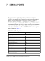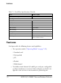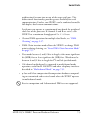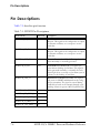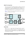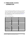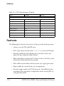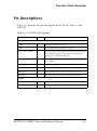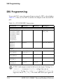
1
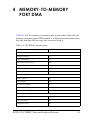
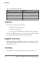
Registers Reference
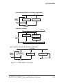
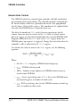
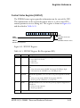
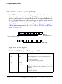
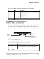
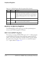
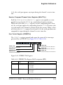
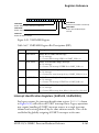
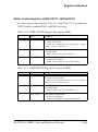
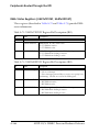
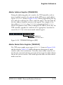
AMI Control Registers (AMICTLx)
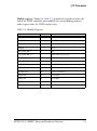
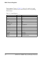
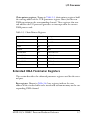
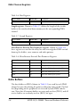
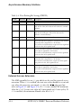
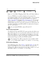
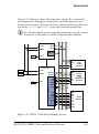
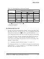
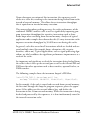
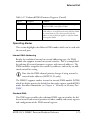
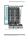
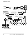
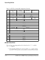
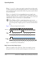
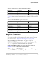
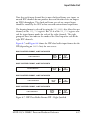
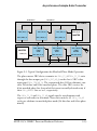
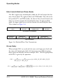
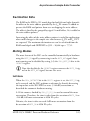
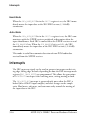
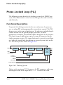
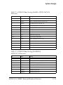
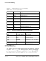
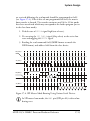
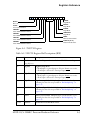
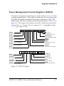
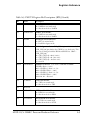
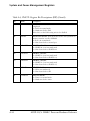
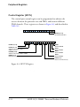
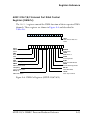
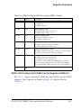
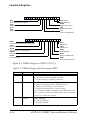
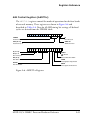
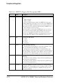
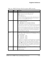
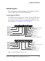
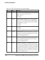
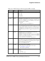
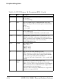
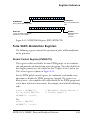
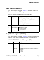
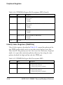
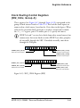
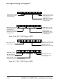
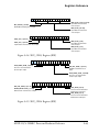
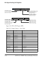
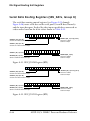
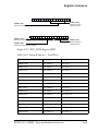
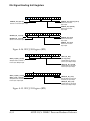
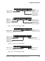
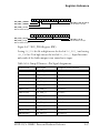
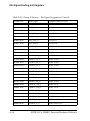
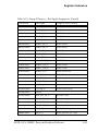
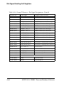
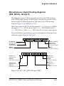
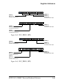
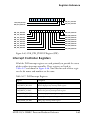
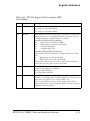
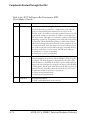
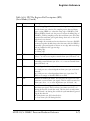
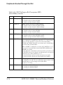
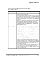
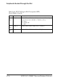
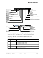
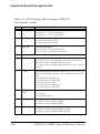
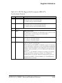
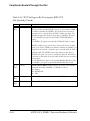
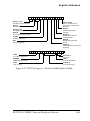
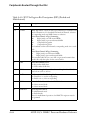
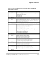
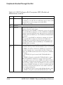
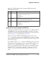
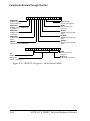
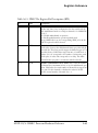
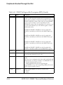
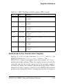
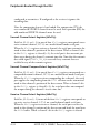
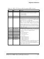
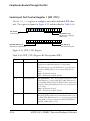
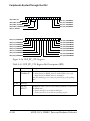
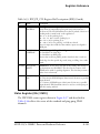
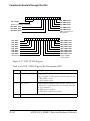
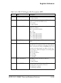
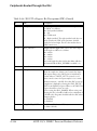
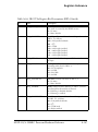
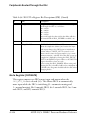
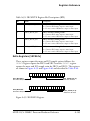
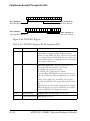
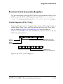
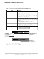
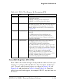
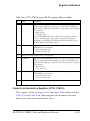
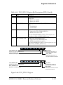
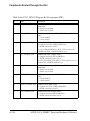
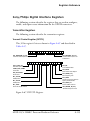
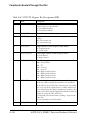
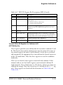
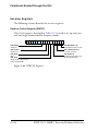
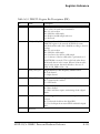
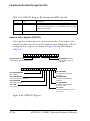
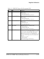
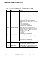
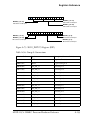
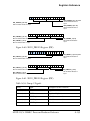
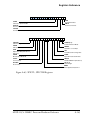
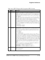
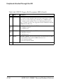
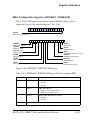
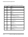
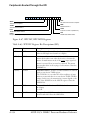
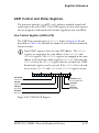
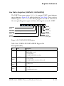
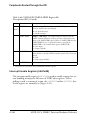
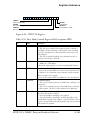
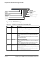
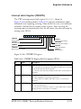
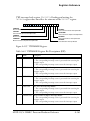
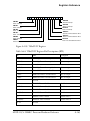
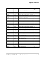
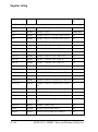
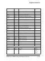
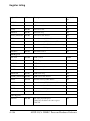
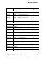
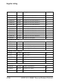
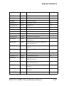
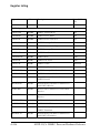
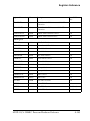
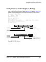
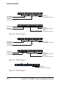
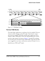
The AMICTL0–3 registers control the mode of operations for the four banks
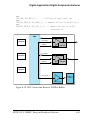
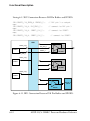
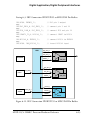
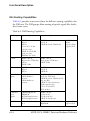
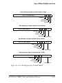
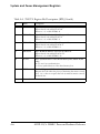
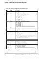
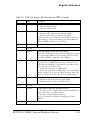
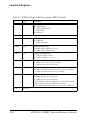
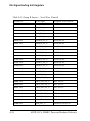
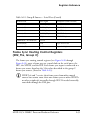
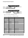
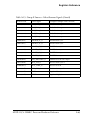
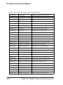
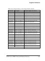
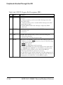
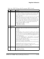
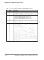
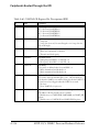
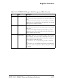
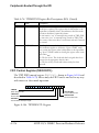
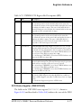
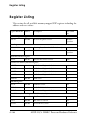
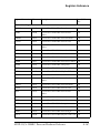
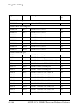
of external memory. These registers are shown in Figure A-6 and
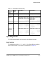
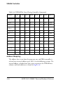
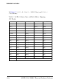
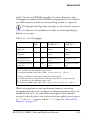
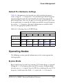
described in Table A-8. Note for all AMI timing bit settings, all defined
cycles are derived from the SDRAM clock.
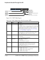
31 30
29 28 27 26 25 24
23 22
21 20 19 18 17 16
PREDIS
Disable Predictive Reads
IC
Bus Idle Cycle
RHC (20–18)
Read Hold Cycle
AMIFLSH
AMI Buffer Flush
15 14 13 12
11 10
9
8
7
6
5
4
3
2
1
IC (16–14)
HC (13–11
Bus Hold Cycle
0
AMIEN
AMI Enable
BW
WS (10–6)
External Data Bus Width
Wait States
PKDIS
ACKEN
ACK Pin Enable
Packing/Unpacking Disable
MSWF
Most Significant Word First
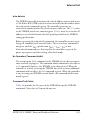
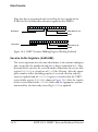
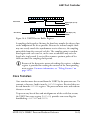
Figure A-6. AMICTLx Registers
ADSP-2137x SHARC Processor Hardware Reference
A-21