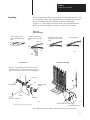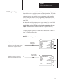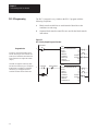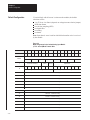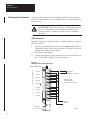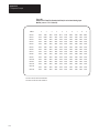
1
Isolated Analog Input Module
Cat. No. 1771-IL Series B
User Manual
Important User Information
Because of the variety of uses for the products described in this
publication, those responsible for the application and use of this control
equipment must satisfy themselves that all necessary steps have been taken
to assure that each application and use meets all performance and safety
requirements, including any applicable laws, regulations, codes
and standards.
The illustrations, charts, sample programs and layout examples shown in
this guide are intended solely for example. Since there are many variables
and requirements associated with any particular installation, Allen-Bradley
does not assume responsibility or liability (to include intellectual property
liability) for actual use based upon the examples shown in this publication.
Allen-Bradley publication SGI–1.1, “Safety Guidelines For The
Application, Installation and Maintenance of Solid State Control”
(available from your local Allen-Bradley office) describes some important
differences between solid-state equipment and electromechanical devices
which should be taken into consideration when applying products such as
those described in this publication.
Reproduction of the contents of this copyrighted publication, in whole or
in part, without written permission of Allen–Bradley Company, Inc.
is prohibited.
Throughout this manual we make notes to alert you to possible injury to
people or damage to equipment under specific circumstances.
ATTENTION: Identifies information about practices or
circumstances that can lead to personal injury or death, property
damage or economic loss.
Attention helps you:
Identify a hazard.
Avoid the hazard.
Recognize the consequences.
Important: Identifies information that is especially important for
successful application and understanding of the product.
Important: We recommend you frequently backup your application
programs on appropriate storage medium to avoid possible data loss.
Summary of Changes
Summary of Changes
Summary of Changes
This release of this publication contains new and revised information from
the last release.
New Information
This manual covers the series B version of the 1771-IL isolated input
module. The 1771-IL series B module has 16-bit resolution, improved
sample time, and auto-calibration.
Revised Information
Many areas in this manual have been modified. Change bars (as shown to
the right side of this paragraph) are used to indicate new or revised
information. Every chapter in this manual has been revised. Please read
carefully.
S-1
Preface
Using This Manual
Purpose of Manual
This manual shows you how to use your Isolated Analog Input module
with an Allen-Bradley programmable controller. It helps you install,
program, calibrate, and troubleshoot your module.
Audience
You must be able to program and operate an Allen-Bradley programmable
controller to make efficient use of your input module. In particular, you
must know how to program block transfers.
We assume that you know how to do this in this manual. If you do not,
refer to the appropriate programming and operations manual for your
programmable controller before you attempt to program this module.
Vocabulary
In this manual, we refer to:
- the 1771-IL series B analog input module as the “input module,” or
the “1771-IL/B”
- the Programmable Controller as the “controller”
Manual Organization
This manual is divided into seven chapters. The following chart shows
each chapter with its corresponding title and a brief overview of the topics
covered in that chapter.
Chapter
Title
Topics Covered
1
Overview of the input module
Description of the module including general and
hardware features
2
Installing the module
Module power requirements, keying, chassis
location
Wiring of the field wiring arm
3
Communicating with your
module
Reading data from your module
Sample programs
4
Configuring your module
Hardware and software configuration
Input range selection
Data format
5
Module status and input data
Reading data from the module
6
Calibrating your module
Information on calibrating your module
7
Troubleshooting
Troubleshooting guide for problem diagnosis
P-1
Preface
Using This Manual
Appendix
Related Products
Title
Topics Covered
A
Specifications
B
Configuration Example
C
Data Formats
D
Block transfer with Mini-PLC-2
How to use GET-GET instructions
and PLC-2/20 processors
Information on BCD, 2s complement binary, signed
magnitude
You can install your input module in any system that uses Allen-Bradley
programmable controllers with block transfer capability and the 1771 I/O
structure.
Contact your nearest Allen-Bradley office for more information about your
programmable controllers.
Product Compatibility
The 1771-IL series B module can be used with any 1771 I/O chassis.
Communication between the analog module and the processor is
bidirectional; the processor block-transfers output data through the output
image table to the module and block-transfers input data from the module
through the input image table. The module also requires an area in the data
table to store the read block and write block. I/O image table use is an
important factor in module placement and addressing selection. The
module’s data table use is listed in Table P.A.
Table P.A
Compatibility and Use of Data Table
Use of Data Table
Catalog
Number
mb
1771-IL/B
Input
Image
m
Bits
8
Output ReadImage
m
Blocks
ck
Bits
Words
8
15
A = Compatible with 1771-A1, -A2, -A4
B = Compatible with 1771-A1B, -A2B, -A3B, -A4B
Y = Compatible without restriction.
P-2
Compatibility
Addressing
WriteBlock
ck
Words
1/2-Slot
1-Slot
2-slot
37
Y
Y
Y
Chassis
Series
A, B
Preface
Using This Manual
You can place your input module in any I/O module slot of the I/O chassis.
You can put two input modules in the same module group. You can put an
input and an output module in the same module group.
Do not put the module in the same module group as a discrete high density
module unless using 1- or 2-slot addressing. Avoid placing output modules
close to ac modules or high voltage dc modules.
Related Publications
For a list of publications with information on Allen-Bradley programmable
controller products, consult our publication index (SD499).
P-3
Table of Contents
Overview of the Input
Module
Chapter 1
Installing the Input Module
Chapter 2
Chapter Objectives . . . . . . . . . . . . . . . . . . . . . . . . . . . . . . . . . . . . . . . . .
Module Descriptions . . . . . . . . . . . . . . . . . . . . . . . . . . . . . . . . . . . . . . . .
Features . . . . . . . . . . . . . . . . . . . . . . . . . . . . . . . . . . . . . . . . . . . . . . . . . .
How Analog Modules Communicate with Programmable Controllers .
Accuracy . . . . . . . . . . . . . . . . . . . . . . . . . . . . . . . . . . . . . . . . . . . . . . . . .
Chapter Summary . . . . . . . . . . . . . . . . . . . . . . . . . . . . . . . . . . . . . . . . . .
Chapter Objectives . . . . . . . . . . . . . . . . . . . . . . . . . . . . . . . . . . . . . . . . .
Before You Install Your Input Module . . . . . . . . . . . . . . . . . . . . . . . . . .
Electrostatic Damage . . . . . . . . . . . . . . . . . . . . . . . . . . . . . . . . . . . . . . . .
Power Requirements . . . . . . . . . . . . . . . . . . . . . . . . . . . . . . . . . . . . . . . .
Module Location in the I/O Chassis . . . . . . . . . . . . . . . . . . . . . . . . . . . .
Module Keying . . . . . . . . . . . . . . . . . . . . . . . . . . . . . . . . . . . . . . . . . . . .
Wiring Your Input Module . . . . . . . . . . . . . . . . . . . . . . . . . . . . . . . . . . .
Grounding . . . . . . . . . . . . . . . . . . . . . . . . . . . . . . . . . . . . . . . . . . . . . . . .
Setting the Voltage/Current Selection Jumpers . . . . . . . . . . . . . . . . . . . .
Module Installation . . . . . . . . . . . . . . . . . . . . . . . . . . . . . . . . . . . . . . . . .
Indicator Lights . . . . . . . . . . . . . . . . . . . . . . . . . . . . . . . . . . . . . . . . . . . .
Chapter Summary . . . . . . . . . . . . . . . . . . . . . . . . . . . . . . . . . . . . . . . . . .
Communicating With Your
Module
Chapter 3
Configuring Your Module
Chapter 4
Chapter Objectives . . . . . . . . . . . . . . . . . . . . . . . . . . . . . . . . . . . . . . . . .
Block Transfer Programming . . . . . . . . . . . . . . . . . . . . . . . . . . . . . . . . .
PLC-2 Programming . . . . . . . . . . . . . . . . . . . . . . . . . . . . . . . . . . . . . . . .
PLC-3 Programming . . . . . . . . . . . . . . . . . . . . . . . . . . . . . . . . . . . . . . . .
PLC-5 Programming . . . . . . . . . . . . . . . . . . . . . . . . . . . . . . . . . . . . . . . .
Module Scan Time . . . . . . . . . . . . . . . . . . . . . . . . . . . . . . . . . . . . . . . . . .
Chapter Summary . . . . . . . . . . . . . . . . . . . . . . . . . . . . . . . . . . . . . . . . . .
Chapter Objectives . . . . . . . . . . . . . . . . . . . . . . . . . . . . . . . . . . . . . . . . .
Configuring Your Input Module . . . . . . . . . . . . . . . . . . . . . . . . . . . . . . .
Input Range Selection . . . . . . . . . . . . . . . . . . . . . . . . . . . . . . . . . . . . . . .
Block Transfer Write Format . . . . . . . . . . . . . . . . . . . . . . . . . . . . . . . . . .
Data Format . . . . . . . . . . . . . . . . . . . . . . . . . . . . . . . . . . . . . . . . . . . . . . .
Digital Filtering . . . . . . . . . . . . . . . . . . . . . . . . . . . . . . . . . . . . . . . . . . . .
Real Time Sampling . . . . . . . . . . . . . . . . . . . . . . . . . . . . . . . . . . . . . . . .
Scaling . . . . . . . . . . . . . . . . . . . . . . . . . . . . . . . . . . . . . . . . . . . . . . . . . . .
Default Configuration . . . . . . . . . . . . . . . . . . . . . . . . . . . . . . . . . . . . . . .
Chapter Summary . . . . . . . . . . . . . . . . . . . . . . . . . . . . . . . . . . . . . . . . . .
1-1
1-1
1-1
1-2
1-3
1-3
2-1
2-1
2-1
2-2
2-2
2-2
2-3
2-5
2-6
2-7
2-7
2-8
3-1
3-1
3-2
3-3
3-4
3-5
3-5
4-1
4-1
4-2
4-3
4-4
4-4
4-5
4-7
4-10
4-13
I
Table of Contents
Module Status and Input
Data
Chapter 5
Calibrating Your Module
Chapter 6
Chapter Objectives . . . . . . . . . . . . . . . . . . . . . . . . . . . . . . . . . . . . . . . . . 5-1
Reading Data From Your Module . . . . . . . . . . . . . . . . . . . . . . . . . . . . . . 5-1
Chapter Summary . . . . . . . . . . . . . . . . . . . . . . . . . . . . . . . . . . . . . . . . . . 5-3
Chapter Objective . . . . . . . . . . . . . . . . . . . . . . . . . . . . . . . . . . . . . . . . . .
Tools and Equipment . . . . . . . . . . . . . . . . . . . . . . . . . . . . . . . . . . . . . . . .
Calibrating your Input Module . . . . . . . . . . . . . . . . . . . . . . . . . . . . . . . .
About Auto-calibration . . . . . . . . . . . . . . . . . . . . . . . . . . . . . . . . . . . . . .
Performing Auto-calibration . . . . . . . . . . . . . . . . . . . . . . . . . . . . . . . . . .
Chapter Summary . . . . . . . . . . . . . . . . . . . . . . . . . . . . . . . . . . . . . . . . . .
Troubleshooting
6-1
6-1
6-1
6-1
6-2
6-5
Chapter 7
Chapter Objective . . . . . . . . . . . . . . . . . . . . . . . . . . . . . . . . . . . . . . . . . . 7-1
Diagnostics Reported by the Module . . . . . . . . . . . . . . . . . . . . . . . . . . . 7-1
Status Reported by the Module . . . . . . . . . . . . . . . . . . . . . . . . . . . . . . . . 7-2
Specifications
Appendix A
Specifications . . . . . . . . . . . . . . . . . . . . . . . . . . . . . . . . . . . . . . . . . . . . . A-1
Configuration Example
Appendix B
Sample Configuration of the Analog Input Module . . . . . . . . . . . . . . . . B-1
Data Formats
Appendix C
4–Digit Binary Coded Decimal (BCD) . . . . . . . . . . . . . . . . . . . . . . . . . . C-1
Signed–magnitude Binary . . . . . . . . . . . . . . . . . . . . . . . . . . . . . . . . . . . . C-2
Two’s Complement Binary . . . . . . . . . . . . . . . . . . . . . . . . . . . . . . . . . . . C-2
Block Transfer (Mini–PLC–2
and PLC–2/20 Processors)
II
Appendix D
Multiple GET Instructions–Mini–PLC–2 and PLC–2/20 Processors . . . D-1
Setting the Block Length (Multiple GET Instructions only) . . . . . . . . . . D-3
Chapter
1
Overview of the Input Module
Chapter Objectives
This chapter gives you information on:
features of the module
how the input module communicates with programmable
controllers
Module Descriptions
The input module is an intelligent block transfer module that interfaces
analog input signals with any Allen-Bradley programmable controllers that
have block transfer capability. Block transfer programming moves input
data words from the module’s memory to a designated area in the
processor data table in a single scan. It also moves configuration words
from the processor data table to module memory.
The input module is a single-slot module that requires no external power
supply. After scanning the analog inputs, the input data is converted to a
specified data type in a digital format to be transferred to the processor’s
data table on request. The block transfer mode is disabled until this input
scan is complete. Consequently, the minimum interval between block
transfer reads is the same as the total input update time for each analog
input module.
Features
This module senses up to eight analog signals at its inputs and converts
them to a proportional four-digit BCD or 16-bit binary value while
providing channel to channel and channel to ground isolation of +1000V.
You can select from five voltage or three current input ranges. Each input
is software selectable on a per channel basis.
This module’s features include:
Eight software configurable differential inputs
User program selectable input ranges on a per channel basis (see
Table 1.A)
Selectable real-time sampling
Selectable scaling to engineering units
Selectable digital filtering
+1000V input isolation, channel-to-channel, channel-to-ground
Selectable high and low input alarms
1-1
Chapter 1
Overview of the Input Module
Table 1.A
Program Selectable Input Ranges
Voltage Ranges
Current Ranges
1 to 5V dc
4 to 20mA
0 to 5V dc
0 to 20mA
-5 to +5V dc
-20 to +20mA
-10 to +10V dc
0 to 10V dc
How Analog Modules
Communicate with
Programmable Controllers
The processor transfers data to the module (block transfer write, BTW) and
from the module (block transfer read, BTR) using BTW and BTR
instructions in your ladder diagram program. These instructions let the
processor obtain input values and status from the module, and let you
establish the module’s mode of operation (Figure 1.1).
1.
The processor transfers your configuration data, and alarm values to
the module via a block transfer write instruction.
2.
External devices generate analog signals that are transmitted to the
module.
Figure 1.1
Communication Between Processor and Module
3
5
6
I/O Chassis
Backplane
2
+
-
4
1
Input Module
Cat. No. 1771-IL/B
1-2
Programmable Controller
11845-I
Chapter 1
Overview of the Input Module
3.
The module converts analog signals into binary or BCD format, and
stores these values until the processor requests their transfer.
4.
When instructed by your ladder program, the processor performs a
read block transfer of the values and stores them in a data table.
5.
The processor and module determine that the transfer was made
without error, and that input values are within specified range.
6.
Your ladder program can use and/or move the data (if valid) before it
is written over by the transfer of new data in a subsequent transfer.
7.
Your ladder program should allow write block transfers to the module
only when enabled by operator intervention or at power-up.
Accuracy
The accuracy of your input module is described in Appendix A.
Chapter Summary
In this chapter you read about the functional aspects of the input module
and how the module communicates with the programmable controller.
1-3
Chapter
2
Installing the Input Module
Chapter Objectives
This chapter gives you information on:
calculating the chassis power requirement
choosing the module’s location in the I/O chassis
configuring your module voltage/current selection jumpers
keying a chassis slot for your module
wiring the input module’s field wiring arm
installing the input module
Before You Install Your Input
Module
Before installing your input module in the I/O chassis you should:
You need to:
As described under:
Calculate the power requirements of all modules
Power Requirements, page 2-2.
in each chassis.
Electrostatic Damage
Determine where to place the module in the I/O
chassis.
Module Location in the I/O Chassis, page 2-2.
Select the input for each channel.
Setting the Voltage/Current Selection Jumpers,
page 2-2.
Key the backplane connector in the I/O chassis.
Module Keying, page 2-4.
Make connections to the wiring arm.
Wiring Your Input Module, page 2-5, and
Grounding, page 2-7
Electrostatic discharge can damage semiconductor devices inside this
module if you touch backplane connector pins. Guard against electrostatic
damage by observing the following precautions:
ATTENTION: Electrostatic discharge can degrade
performance or cause permanent damage. Handle the module as
stated below.
Wear an approved wrist strap grounding device, or touch a grounded
object to rid yourself of electrostatic charge before handling the module.
Handle the module from the front, away from the backplane connector.
Do not touch backplane connector pins.
Keep the module in its static-shield bag when not in use.
2-1
Chapter 2
Installing the Input Module
Power Requirements
Your module receives its power through the 1771 I/O power supply. The
Isolated Analog input module requires 1.2A at 5V from the power supply.
Add this current to the requirements of all other modules in the I/O chassis
to prevent overloading the chassis backplane and/or backplane
power supply.
Module Location in the I/O
Chassis
Place your module in any I/O module slot of the I/O chassis except for the
extreme left slot. This slot is reserved for programmable controller
processors or adapter modules.
Group your modules to minimize adverse affects from radiated electrical
noise and heat. We recommend the following.
Group analog input and low voltage dc modules away from ac modules
or high voltage dc modules to minimize electrical noise interference.
Do not place this module in the same I/O group with a discrete
high-density I/O module when using 2-slot addressing. This module
uses a byte in both the input and output image tables for block transfer.
After determining the module’s location in the I/O chassis, connect the
wiring arm to the pivot bar at the module’s location.
Setting the Voltage/Current
Selection Jumpers
The Isolated Analog Input Module (1771-IL/B) is shipped with each
channel set for voltage mode. If a milliamp input is desired, you must set a
jumper on the functional analog block (FAB) for that particular channel.
To set the selection jumpers for your desired inputs, proceed as follows:
2-2
1.
Remove the module’s left hand cover plate (the one without
the labels).
2.
Locate the selection plugs (Figure 2.1).
3.
Position the jumpers as shown in Figure 2.1 for your
particular module.
4.
Reassemble the module after you have finished checking and/or
setting the selection plugs.
Chapter 2
Installing the Input Module
Figure 2.1
Configuration Jumper Settings for 1771-IL/B Inputs
Voltage/Current
Jumper
Functional Analog Block
Channel 1
Channel 2
Channel 3
Channel 4
Channel 5
Jumper in
Jumper in
Current position. Voltage position.
Channel 6
Channel 7
Channel 8
Edge View
(enlarged)
Side View
11847-I
2-3
Chapter 2
Installing the Input Module
Installing the Analog Module
To install your module in an I/O chassis:
1.
First, turn off power to the I/O chassis:
ATTENTION: Remove power from the 1771 I/O chassis
backplane and disconnect the cable from the module before
removing or installing an I/O module.
Failure to remove power from the backplane could cause injury
or equipment damage due to possible unexpected operation.
Failure to remove power from the backplane could cause
module damage, degradation of performance, or injury.
locking-bar pins
2.
Lift the locking latch holding the module into the chassis. (On chassis
equipped with a chassis locking bar, pull the locking-bar pins to
release the locking bar and swing it up.)
3.
Position the keying bands (Figure 2.2) in the backplane connectors to
correspond to the key slots on the module. This prevents you from
inserting the wrong module in this slot. This analog module uses:
front of chassis
12453-I
between 10 and 12
between 32 and 34
ATTENTION: Observe the following precautions when
inserting or removing keys:
insert or remove keys with your fingers
make sure that key placement is correct
Incorrect keying or the use of a tool can result in damage to
the backplane connector and possible system faults.
You can change the position of these bands if subsequent system
design and rewiring makes insertion of a different type of module
necessary. Use needlenose pliers to insert or remove keying bands.
2-4
Chapter 2
Installing the Input Module
Figure 2.2
Keying Positions
I/O chassis
Keying Bands
Keying Band Location
Between 10 and 12
Between 32 and 34
ATTENTION: Insert or remove
keying bands with your fingers.
Upper Connector
Connecting Wiring to Your
Input Module
11022-I
4.
Place the module in the plastic tracks on the top and bottom of the
slot that guides the module into position.
5.
Do not force the module into its backplane connector. Apply firm
even pressure on the module until it is firmly seated in the chassis.
Note: The chassis locking bar will not close if all modules are not
seated properly.
6.
Snap the chassis locking bar (or locking latch on earlier chassis) over
the top of the module to secure it. Make sure the locking pins on the
locking bar are fully engaged.
7.
Connect the wiring to the module as explained under “Connecting
Wiring” below.
Connect your input devices to the cat. no. 1771-WF wiring arm shipped
with the module. Attach the wiring arm to the pivot bar at the bottom of
the I/O chassis. It pivots upward and connects with the module so you can
install or remove the module without disconnecting the wires.
Connect inputs to the 1771-IL/B module as shown in Figure 2.3. This
module is shipped from the factory configured for voltage inputs but can
be configured for any combination of current and voltage inputs. If you
want to change the configuration, refer to “Setting the Voltage/Current
Selection Jumpers” as explained earlier in this chapter.
Important: The module configuration jumpers must be set for either
voltage or current before inserting the module into the I/O chassis.
2-5
Chapter 2
Installing the Input Module
Figure 2.3
Wiring Connections for the Isolated Analog Input Module (1771-IL/B)
+
17
18
Analog Source
–
15
16
Ground
14
13
+
9
10
11
12
Analog Source
–
Ground
18
17
Channel 1
16
15
Channel 2
14
Channel 3
13
12
11
10
9
8
7
Channel 4
Channel 5
6
5
Channel 6
4
3
Channel 7
7
8
5
6
3
4
2
2
1
1
Channel 8
NOTE: The 1771-IL/B module does not supply loop power for loop
powered analog sources (transmitters, transducers, etc.).
Loop power must be supplied by the user.
Field Wiring Arm
Cat. No. 1771-WF
11846-I
2-6
Chapter 2
Installing the Input Module
Grounding
When using shielded cable wire, ground the foil shield and drain wire only
at one end of the cable. We recommend that you wrap the foil shield and
drain wire together and connect them to a chassis mounting bolt
(Figure 2.4). At the opposite end of the cable, tape exposed shield and
drain wire with electrical tape to insulate it from electrical contact.
Figure 2.4
Cable Grounding
Remove a length of cable
jacket from the Belden 8761
cable.
Pull the foil shield and bare
drain wire from the insulated
wires.
Twist the foil shield and drain
wire together to form a single
strand.
Attach a ground lug.
Bare drain
wire
Belden 8761 Cable
Insulated
wires
20104
Foil
shield
Chassis Ground
Single-point Grounding
When you connect grounding conductors to the I/O chassis
grounding stud, place a star washer under the first lug, then
place a nut with captive lock washer on top of each ground lug.
Ground Lug
Nut
Nut and Captive
Washer
Grounding Stud
Star
Washer
I/O Chassis Side Plate
Ground Lug1
19923
19480
1Use the cup washer if crimp-on lugs are not used.
#10 Thread-forming screw
External-tooth Washers
Refer to Wiring and Grounding Guidelines, publication 1770-4.1, for additional information.
2-7
Chapter 2
Installing the Input Module
Indicator Lights
The front panel of the input module contains a green RUN and a red FLT
(fault) indicator (Figure 2.5). At powerup, an initial module self-check
occurs. If there is no fault, the red indicator turns off. The green indicator
will blink until the processor completes a successful write block transfer to
the module. Upon completion of a block transfer write (BTW), the green
RUN indicator will be on and the red FLT indicator will be off. If a fault is
found initially or occurs later, the red FLT indicator lights. Possible module
fault causes and corrective actions are discussed in Chapter 7,
Troubleshooting.
Figure 2.5
Diagnostic Indicators
ISOLATED
ANALOG INPUT
RUN
FLT
10528-I
Chapter Summary
2-8
In this chapter you learned how to install your input module in an existing
programmable controller system and how to wire to the field wiring arm.
Chapter
3
Communicating With Your Module
Chapter Objectives
In this chapter, we describe
block transfer programming
quick-start sample programs in the PLC-2, PLC-3 and PLC-5
processors
module scan time issues
Block Transfer
Programming
Your module communicates with your processor through bidirectional
block transfers. This is the sequential operation of both block transfer read
(BTR) and block transfer write (BTW) instructions.
A configuration BTW is initiated when the analog module is first powered
up, and subsequently only when the programmer wants to enable or disable
features of the module. The configuration BTW sets the bits which enable
the programmable features of the module, such as scaling, alarming, real
time sampling, etc. Block Transfer reads are performed to retrieve
information from the module.
Subsequent BTWs occur only when the programmer wants to write a new
configuration to the module. At all other times the module is basically in a
repetitive block transfer read (BTR) mode.
The following example programs are minimum programs; all rungs and
conditioning must be included in your application program. You can
disable BTRs, or add interlocks to prevent writes if desired. Do not
eliminate any storage bits or interlocks included in the sample programs. If
interlocks are removed, the program may not work properly.
The analog input module will work with a default configuration of
zeroes entered in the configuration block. This results in the default
settings of: 1 to 5V dc or 4 to 20mA (depending on voltage/current
selection jumper), BCD data format, no real time sampling (RTS), no
digital filter, no scaling, and no alarms. Refer to Chapter 4 for more
information. Also, refer to Appendix B for example configuration blocks
and instruction addresses to get started.
Your program should monitor status bits (such as overrange, underrange,
alarms, etc.) and block transfer read activity.
The following example programs illustrate the minimum programming
required for the 1771-IL series B module to powerup and operate.
3-1
Chapter 3
Communicating With Your Module
PLC-2 Programming
The PLC-2 program example regulates when each block transfer will be
initiated to eliminate problems caused by limited regulation of
bidirectional block transfers. Both storage bits are needed, (as shown in the
example), to accomplish this task in all PLC-2 systems, local or remote,
with long or short program scans. Therefore, the program as shown is the
minimum required. Note that PLC-2 processors that do not have the block
transfer instruction must use the GET-GET block transfer format which is
outlined in appendix D.
Figure 3.1
PLC-2 Family Sample Program Structure
Block Transfer Read
Done Bit
Program Action
FILE TO FILE MOVE
COUNTER ADDR:
XXX
POSITION:
XXX
XXX
FILE LENGTH:
FILE A:
XXXX – XXXX
FILE R:
XXXX – XXXX
RATE PER SCAN
XXX
1
Rung 1
Block transfer read buffer: the file-to-file
move instruction holds the block transfer
read (BTR) data (file A) until the
processor checks the data integrity. If the
data was successfully transferred, the
processor energizes the BTR done bit,
initiating a data transfer to the buffer (file
R) for use in the program. If the data is
Pushbutton [1]
corrupted during the BTR operation, the 2
BTR done bit is not energized and data
is not transferred to the buffer file. In this
Block Transfer Write
case, the data in the BTR file will be
Done Bit
overwritten by data from the next BTR.
Pushbutton [1]
3
Rungs 6 and 7
These rungs are the conditioning block
transfer rungs. Include all the input
7
conditioning shown in the example
program.
Power–up
Bit
Storage
Bit A
Storage
Bit A
Power-up
Bit
BTR Done
Bit
Storage
Bit B
Storage
Bit B
U
BTR
BLOCK XFER READ
DATA ADDR:
XXX
RGS
MODULE ADDR:
XX
BLOCK LENGTH:
FILE:
XXXX – XXXX
ENABLE
EN
X7
DONE
DN
X7
BTW
BLOCK XFER WRITE
XXX
DATA ADDR:
RGS
MODULE ADDR:
BLOCK LENGTH:
XX
FILE:
XXXX – XXXX
[1] You can replace the pushbutton with a timer “done” bit to initiate the block transfer
write on a timed basis. You can also use any storage bit in memory.
3-2
Storage
Bit A
U
Storage
Bit B
L
Storage
Bit B
Power–up
Bit
DONE
DN
15
Storage
Bit A
L
Rungs 2 and 3
Block Transfer Write
These rungs provide for a user-initiated
Done Bit
block transfer write (BTW) after the
4
module is initialized at power-up.
Pressing the pushbutton locks out BTR
operation and initiates a BTW that
Block Transfer Read
reconfigures the module. Block transfer
Done Bit
writes will continue for as long as the
5
pushbutton remains closed.
Rungs 4 and 5
These rungs provide a “read-write-read”
6
sequence to the module at power-up.
They also insure that only one block
transfer (read or write) is enabled during
a particular program scan.
ENABLE
EN
17
ENABLE
EN
X6
DONE
DN
X6
Chapter 3
Communicating With Your Module
PLC-3 Programming
Block transfer instructions with the PLC-3 processor use one binary file in
a data table section for module location and other related data. This is the
block transfer control file. The block transfer data file stores data that you
want transferred to your module (when programming a block transfer
write) or from your module (when programming a block transfer read).
The address of the block transfer data files are stored in the block transfer
control file.
The industrial terminal prompts you to create a control file when a block
transfer instruction is being programmed. The same block transfer
control file is used for both the read and write instructions for your
module. A different block transfer control file is required for every
module.
A sample program segment with block transfer instructions is shown in
Figure 3.2, and described below.
Figure 3.2
PLC-3 Family Sample Program Structure
Program Action
At power-up, the user program enables a
1
block transfer read. Then it initiates a block
transfer write to configure the module.
Block Transfer
Read Done Bit
Block Transfer
Write Done Bit
Thereafter, the program continuously
performs read and write block transfers.
2
BTR
BLOCK XFER READ
RACK:
XXX
GROUP:
X
MODULE:
X = XXXX
DATA:
XXXX:XXXX
LENGTH:
00
CNTL:
XXXX:XXXX
BTW
BLOCK XFER WRITE
RACK:
XXX
GROUP:
X
MODULE:
X = XXXX
DATA:
XXXX:XXXX
LENGTH:
00
CNTL:
XXXX:XXXX
Enable
EN
12
Done
DN
15
Error
ER
13
Enable
EN
02
Done
DN
05
Error
ER
03
3-3
Chapter 3
Communicating With Your Module
PLC-5 Programming
The PLC-5 program is very similar to the PLC-3 program with the
following exceptions:
1.
Block transfer enable bits are used instead of done bits as the
conditions on each rung.
2.
Separate block transfer control files are used for the block transfer
instructions.
Figure 3.3
PLC-5 Family Sample Program Structure
Program Action
BTR Enable
Bit
BTR
BLOCK TRANSFER READ
1
RACK:
GROUP:
MODULE:
CONTROL:
DATA FILE:
LENGTH:
CONTINUOUS:
At power-up, the program enables a block
transfer read (rung 1). Then it examines the
power-up bit in the BTR file and initiates one
block transfer write to configure the module
(rung 2).
Thereafter, the program continuously reads
data from the module (rung 1). A subsequent
BTW operation is enabled by a pushbutton
switch (rung 2). Changing the processor
mode will not initiate a block transfer write.
Pushbutton
2
Power–up Bit
3-4
BTW Enable Bit
X
X
X
XXX:XX
XXX:XX
00
EN
DN
ER
N
BTW
BLOCK TRANSFER WRITE
X
RACK:
X
GROUP:
X
MODULE:
XXX:XX
CONTROL:
XXX:XX
DATA FILE:
00
LENGTH:
CONTINUOUS:
N
EN
DN
ER
Chapter 3
Communicating With Your Module
Module Scan Time
Scan time is defined as the amount of time it takes for the input module to
read the input channels and place new data into the data buffer. Scan time
for your module is shown in Appendix A.
Figure 3.4
Block Transfer Time
Module available
to perform block transfer
End of Block
Transfer Write
Block
Transfer
Write
Time
1
Configure
Time
1st Scan
2
3
2nd Scan
4
5
3rd Scan
6
10529-I
Internal Scan time = 50ms
T = 100ms, 200ms, 300ms, 3.1s.
The following description references the sequence numbers in Figure 3.4.
Following a block transfer write (1) the module inhibits communication
until after it has loaded the new configuration data (2), scanned the inputs
and/or outputs (3), and filled the data buffer (4). Configuration block
transfers, therefore, should only be performed when the module is being
configured or calibrated.
Any time after the buffer is filled (4), a block transfer read (BTR) request
can be acknowledged.
When operated in the default mode, new data will be available for a BTR
every 50 milliseconds. When operated in real time sample mode
(RTS = T), BTRs will be ignored by the module for “T” milliseconds, at
which time a single BTR will be allowed.
Chapter Summary
In this chapter, you learned how to program your programmable
controller. You were given sample programs for your PLC-2, PLC-3 and
PLC-5 family processors.
You also read about module scan time.
3-5
Chapter
4
Configuring Your Module
Chapter Objectives
In this chapter you will read how to:
configure your module’s hardware
condition your inputs
enter your configuration data.
Configuring Your Input
Module
Because of the many analog devices available and the wide variety of
possible configurations, you must configure your module to conform to the
analog device and specific application that you have chosen. Data is
conditioned through a group of data table words that are transferred to the
module using a block transfer write instruction. Before continuing, make
sure you read “Setting Voltage/Current Selection Jumpers” in
chapter 2.
The software configurable features available with the Isolated Analog
Input Module (1771-IL series B) are:
input range selection
data format
digital filtering
real time sampling
scaling to engineering units
high and low alarms
Configure your module for its intended operation by means of your
programming terminal and block transfer write (BTW) instructions.
Note: Programmable controllers that use 6200 software programming tools
can take advantage of the IOCONFIG utility to configure this module.
IOCONFIG uses menu-based screens for configuration without having to
set individual bits in particular locations. Refer to your 6200 software
literature for details.
Note: Programmable controllers that use process configuration and
operation software (cat. no. 6190-PCO) can take advantage of those
development and runtime tools used for the application of programmable
controllers in process control. The PCO worksheets and the menu-driven
configuration screens and faceplates let you configure, test/debug and
operate the I/O module. Refer to your 6190-PCO software literature for
details.
4-1
Chapter 4
Module Configuration
During normal operation, the processor transfers from 1 to 37 words to the
module when you program a BTW instruction to the module’s address.
The BTW file contains configuration words, high and low channel alarm
settings, and calibration values for each channel.
When a block transfer write length of 0 is programmed, the 1771-IL
series B will respond with the Series A default length of 19.
Input Range Selection
Individual inputs are configurable to operate with any one of five voltage
or three current ranges. You can select individual channel ranges using the
designated words of the write block transfer instruction (Table 4.A). Two
bits are allocated for each channel. For example, for channel 1, set bits 00
and 01 as follows:
Table 4.A
Bit Settings for Voltage or Current Inputs
Bit 01
Bit 00
Voltage or current input
0
0
1 to 5 V DC, 4 to 20 mA1
0
1
0 to 5 V DC, 0 to 20 mA1
1
0
-5 to +5 V DC, -20 to +20 mA1
1
1
-10 to +10 V DC, 0 to 10 V DC2
1 Current input mode selected by configuration plug.
2 Configurable using bipolar scaling.
The 1771-IL/B has 16-bit resolution across the +10V range. For
compatibility purposes, the default scaling for all ranges is 12-bits (0-4095
or +4095). This allows the series B module to be directly interchangeable
with the series A module. To use the full 16-bit capability, scaling values
must be changed. Refer to “Scaling” later in this chapter.
Table 4.B shows the incremented voltage or current assigned to each bit for
the seven different input ranges. For example, if the channel 1 input range
is 0 to +5V and the actual incoming signal is at mid-range (+2.5V) the
value in the module’s data word, if using default scaling, would be 0000
1000 0000 0000 (binary) or 2048 (decimal). The input (default scaling) is
2048/4096, or 1/2 of full scale.
4-2
Chapter 4
Module Configuration
Table 4.B
Input Voltage and Current Ranges for the Analog Input Module
Nominal Voltage
or Current Range
Default Scaling
BCD Output Range
Voltage or
Current Per Bit
Data from
A/D Converter
Voltage or
Current Per Bit
+1 to +5V
0000 to +4095
0.98mV
3063 to 15316
0.33mV
0 to 5V
0000 to +4095
1.22 mV
32768 to 15316
0.33mV
-5 to +5V
-4095 to +4095
1.22mV
-15316 to 15316
0.33mV
-10 to +10V
-4095 to +4095
2.44mV
-30632 to 30632
0.33mV
0 to +20mA
0000 to +4095
0.0049mA
0 to 15316
0.0013mA
+4 to +20mA
0000 to +4095
0.0039mA
3063 to 15316
0.0013mA
-20 to +20mA
-4095 to +4095
0.0049mA
-15316 to 15316
0.0013mA
Note: Voltage and current input ranges are selectable on a per channel basis.
To get the same resolution available from the A/D converter, scale each
channel as shown in Table 4.C.
Table 4.C
Scaling Endpoints
Voltage/Current
Range
Block Transfer Write Format
Minimum
Scaling Endpoint
Maximum
Scaling Endpoint
+1 to 5V
3063
15316
4 to 20mA
3063
15316
0 to 5V
0
15316
0 to 20mA
0
15316
-5 to 5V
-15316
15316
-20 to 20mA
-15316
15316
-10 to 10V
-30632
30632
0 to 10V
-30632
30632
You select the format to enter values in the block transfer write table. Bit
08 (10 octal) of BTW word 2 sets the parameters for scaling, high and low
alarms, and the digital filter constant.
Decimal Bit 08
Octal Bit 10
BTW Data Format
You must enter all values in:
0
BCD (default)
BCD
1
Two’s Complement Binary
Two’s Complement Binary
4-3
Chapter 4
Module Configuration
Data Format
You must also indicate what format will be used to read data from your
module. Typically, BCD is selected with PLC-2 processors, and 2’s
complement binary is selected with PLC-3 and PLC-5 processors. See
Appendix C for details on data format.
Table 4.D
Selecting the Data Format
Digital Filtering
Decimal Bit 10
(Octal Bit 12)
Decimal Bit 09
(Octal Bit 11)
Data Format
0
0
BCD
0
1
not used
1
0
two’s complement binary
1
1
signed magnitude binary
The analog input module has hardware-based high frequency filters on all
channels to reduce the effect of electrical noise on the input signal.
Software digital filtering is meant to reduce the effect of process noise on
the input signal.
The digital filter equation is a classic first order lag equation (Figure 4.1).
Using a step input change to illustrate the filter response (Figure 4.2), you
can see that when the digital filter constant time elapses, 63.2% of the total
response is reached. Each additional time constant achieves 63.2% of the
remaining response.
Figure 4.1
Digital Filter Equation
t
Yn = Yn-1 +
Where:
4-4
t + TA
(Xn - Yn-1)
Yn = present output, filtered peak voltage (PV)
Y n –1 = previous output, filtered PV
t = module channel update time (seconds)
TA = digital filter time constant (seconds)
X n = present input, unfiltered PV
Chapter 4
Module Configuration
Figure 4.2
Digital Filter Lag Equation Illustration
100%
63%
Amplitude
0
Unfiltered Input
TA = 0.01 sec
TA = 0.5 sec
TA = 0.99 sec
0
0.01
0.5
0.99
Time in Seconds
16723
Digital filter time constant values of .00 BCD to .99 BCD (0.00 to 2.55
binary) (.00 = no filter) are set in bits 00 through 07 of word 3 of the block
transfer write instruction. If an invalid digital filter value is entered
(i.e., .1F BCD), the invalid filter value bit in the block transfer read status
area will be set. If an invalid digital filter value is entered, the module will
not perform digital filtering. If you choose to use the digital filtering
feature, the filter time constant value chosen will apply to all input signals.
Real Time Sampling
The real time sampling (RTS) mode of operation provides data gathered at
precisely timed intervals for use by the processor.
Use RTS for time based functions (such as PID and totalization) in the
PLC. RTS allows accurate time based calculations in local or remote I/O
racks. In the RTS mode the module scans and updates its inputs at a user
defined time interval (T) instead of the default interval. The module
ignores block transfer read (BTR) requests for data until the sample time
period elapses. The BTR of a particular data set occurs only once at the
end of the sample period and subsequent requests for transferred data are
ignored by the module until a new data set is available. If a BTR does not
occur before the the end of the next RTS period, a time-out bit is set in the
BTR status area. When set, this bit indicates that at least one data set was
not transferred to the processor. (The actual number of data sets missed is
unknown.) The time-out bit is reset at the completion of the next BTR.
4-5
Chapter 4
Module Configuration
Set appropriate bits in the BTW data file to enable the RTS mode. You can
select RTS periods ranging from 50 ms to 3.1 seconds in increments of
100ms for the 1771-IL/B. Refer to Table 4.E below for actual bit settings.
Note that the default mode of operation is implemented by placing all
zeroes in bits 11 through 15 (13 through 17 octal).
Table 4.E
Examples of Bit Settings for the Real Time Sample Mode
4-6
Decimal Bits
15
14
13
12
11
Octal Bits
17
16
15
14
13
0
0
0
0
0
No RTS, Default settings: 50ms
0
0
0
0
1
100ms
0
0
0
1
0
200ms
0
0
0
1
1
300ms
0
0
1
0
0
400ms
0
0
1
0
1
500ms
0
0
1
1
0
600ms
0
0
1
1
1
700ms
0
1
0
0
0
800ms
0
1
0
0
1
900ms
0
1
0
1
0
1.0s
0
1
1
1
1
1.5s
1
0
1
0
0
2.0s
1
1
0
0
1
2.5s
1
1
1
1
0
3.0s
1
1
1
1
1
3.1s
Sample
m Time
m P
Period
Chapter 4
Module Configuration
Scaling
Each channel has two scaling points, low and high. The signal value at
these points is fixed. For example, the high scaling point of a +10V output
channel always corresponds to an input signal equal to +10.000V.
To implement the scaling feature, you insert the minimum and maximum
scaled values in the appropriate configuration words.
The format of the scaling values is determined by the BTW format bit (bit
08, word 2). The range in BCD format is +9999. The range in binary
format is +32767.
For example, assume that at 0mA, the device connected to this input
channel is producing 0 psi, and at 20mA it produces 150 psi, and the
1771-IL/B range selected is 4 to 20mA. Extrapolation indicates that at
4mA, the device is producing 30 psi. By setting the low scale value of the
input to 30 and the high scale value to 150, this input channel will report
data in psi. For better resolution, you can multiply both of the scaling
values by the same multiplier as long as both scale values are in the range
of +9999 BCD or +32767 binary. By setting the low scale to 3000 and the
high scale value to 15000, you would report data in units of 0.01 psi
per count.
Maximum resolution can be obtained by setting the low scale value to
-9999 in BCD and the high scale value to +9999 in BCD (-32767 low and
+32767 high in binary).
For example, if in the 1 to 5V mode, the scaling points are 1 and 5 volts.
If you set the scaling to +32767, the maximum the module will display will
be 32767. If 5.1V is applied, the display will be 32767 and the overrange
bit for that channel will be set.
Note: To achieve the 0 to +10V range you must use bipolar scaling. Select
the +10V range and scale for + the actual intended range. If you need 0 to
100 gpm, set scaling values at -100 and +100. You will effectively be
creating a 0 to 10V range that is scaled from 0 to 100.
Implementing the Scaling Feature
You implement the scaling feature by:
1.
Inserting minimum and maximum scaled values in the appropriate
configuration words
2.
If using BCD, and any of the minimum or maximum values are
negative, set the appropriate sign bits in the minimum or maximum
sign bit words.
4-7
Chapter 4
Module Configuration
Scaling Ranges
The maximum range of the scaling values is +9999 BCD or +32767 binary.
These values must be entered in the format selected in word 2, bit 08 (10).
If invalid values are entered into the scaling words, the corresponding
input in the BTR data will be zero and the invalid scaling bit will be set.
Table 4.F
Default Scaling Values
Input Range
Default Scaling Value
-10 to +10V
-5 to +5V
-4095
4 95 to +4095
4 95
0 to 5V
1 to 5V
0 to +4095
4 95
If scaling and alarms are not selected, the module still requires specific
BTR and BTW file lengths for the number of channels used. Table 4.G
shows the required BTR and BTW file lengths.
Table 4.G
Block Transfer Read and Write File Lengths (with no scaling or alarms)
Channels Used
BTR File Length
BTW File Length
1
5
5
2
6
7
3
7
9
4
8
11
5
9
13
6
10
15
7
11
17
8
12
19
Important: Use decimally addressed bit locations for PLC-5 processors.
4-8
Chapter 4
Module Configuration
Alarms
Each input channel has alarm functions that provide status indication
through associated status bits in the block transfer read data returned by
the module.
Underrange alarm - This bit is set if the input falls below the minimum
range for that specific input type. This alarm is predefined and cannot be
changed by the user. In current loop inputs, this bit also indicates an
open loop.
Overrange alarm - This bit is set if the input rises above the maximum
range for that specific input type. This alarm is predefined and cannot be
changed by the user. For all voltage inputs, this bit indicates an
open channel.
Underrange Bit is set
when the input signal is
less than:
Overrange Bit is set
when the input signal is
greater than:
1 to 5V/4 to 20mA
1V dc or 4mA
5V dc or 20mA
0 to 5V/0 to 20mA
Zero
5V dc or 20mA
-5 to 5V/-20 to 20mA
-5V dc or -20mA
5V dc or 20mA
-10 to +10V
-10V dc
+10V dc
Range
User-defined alarms let the user specify a range of “good” input values. If
the input value goes outside of this range, the module will set the low or
high alarm bit for that channel. The alarm values are written to the module
in the same units as the scaling values. Valid alarm values are +9999 BCD
or +32767 binary. If you select “no alarms” you must set both the low
alarm value and the high alarm value to zero. If either the low or high
alarm for a channel is not zero, alarms for that channel are enabled.
Figure 4.3
Alarm Example
Overrange Limit
alarm inactive
alarm active
User-Defined High Alarm Limit
Input Channel
User-Defined Low Alarm Limit
Underrange Limit
Time
4-9
Chapter 4
Module Configuration
Default Configuration
If a write block with all zeroes is written to the module, the default
selections will be:
1 to 5V dc or 4 to 20mA (depends on voltage/current selection jumper)
BCD data format
no real time sampling (RTS)
no digital filter
no scaling
no alarms
Note: Input data is set to 0 until an initial block transfer write is received
by the module.
Figure 4.4
Word Assignments for the Isolated Analog Input Module
(1771-IL series B)Block Transfer Write
Decimal Bits
15
14
13
12
11
10
09
08
07
06
05
04
03
02
01
00
Octal Bits
17
16
15
14
13
12
11
10
07
06
05
04
03
02
01
00
Range Selection Bits for Channels 1 through 8
Word 1
8
2
7
6
Data
Format
Real Time Sampling
8
7
6
5
5
4
3
2
4
3
BTW
Format
1
2
1
Digital Filter
8
7
6
5
4
3
3
Sign bits, maximum scaling values
4-10
Sign bits, minimum scaling values
4
Channel 1 - minimum scaling
5
Channel 1 - maximum scaling
6
Channel 2 - minimum scaling
7
Channel 2 - maximum scaling
8
Channel 3 - minimum scaling
9
Channel 3 - maximum scaling
10
Channel 4 - minimum scaling
11
Channel 4 - maximum scaling
12
Channel 5 - minimum scaling
13
Channel 5 - maximum scaling
14
Channel 6 - minimum scaling
15
Channel 6 - maximum scaling
16
Channel 7 - minimum scaling
2
1
Chapter 4
Module Configuration
Decimal Bits
15
14
13
12
11
10
09
08
07
06
05
04
03
02
01
00
Octal Bits
17
16
15
14
13
12
11
10
07
06
05
04
03
02
01
00
6
5
4
3
2
1
G
O
17
Channel 7 - maximum scaling
18
Channel 8 - minimum scaling
19
Channel 8 - maximum scaling
8
7
6
5
4
3
2
1
8
7
2
20
Sign bits, low alarm values
Sign bits, high alarm values
21
Channel 1 - Low Alarm Value
22
Channel 1 - High Alarm Value
23
Channel 2 - Low Alarm Value
24
Channel 2 - High Alarm Value
25
Channel 3 - Low Alarm Value
26
Channel 3 - High Alarm Value
27
Channel 4 - Low Alarm Value
28
Channel 4 - High Alarm Value
39
Channel 5 - Low Alarm Value
30
Channel 5 - High Alarm Value
31
Channel 6 - Low Alarm Value
32
Channel 6 - High Alarm Value
33
Channel 7 - Low Alarm Value
34
Channel 7 - High Alarm Value
35
Channel 8 - Low Alarm Value
36
Channel 8 - High Alarm Value
8
7
6
5
4
3
2
1
Not Used
S
37
Inhibit bits for calibration
Calibration bits
4-11
Chapter 4
Module Configuration
Bit/Word Descriptions for the Isolated Analog Input Module
Configuration Block
Note that decimal bits are shown. Octal bits are shown in parentheses.
Word
Decimal Bit
(Octal Bit)
Description
Word 1
Bits 00-15
(00-17)
Input range selections, grouped 2 bits for each channel, allow selection of any
of 7 input voltage or current ranges. See Table 4.A.
Bits 00-07
Digital filter reduces effect of noise on the input. See “Digital Filtering.”
Bit 08 (10)
BTW format bit. This bit determines the format for scaling, digital filter
constant, and high and low alarms.
Bit 08 (10) = 0 - Values must be entered in BCD
Bit 08 (10) = 1 - Values must be entered in Two’s Complement Binary
Bits 09-10
(11-12)
Data format is used to match format of processor. See Table 4.D.
Bits 11-15
(13-17)
Real time sampling defaults to 50ms if zeroes are entered. See Table 4.E
for other real time sample intervals.
Bits 00-07
Minimum sign bits, when set, designate minimum scaling values that are
negative in BCD. Default = 0 - positive.
Bits 08-15
(10-17)
Maximum sign bits, when set, designate maximum scaling values that are
negative in BCD. Default = 0 - positive.
Word 4
Bits 00-15
(00-17)
Minimum scaling values for channel 1. Enter in format selected in word 2,
bit 08 (10). Valid entries are between +9999 and -9999 in BCD; -32767 and
+32767 in binary. Default = 0 - no scaling.
Word 5
Bits 00-15
(00-17)
Maximum scaling values for channel 1. Enter in format selected in word 2,
bit 08 (10). Valid entries are between +9999 and -9999; -32767 and +32767
in binary. Default = 0 - no scaling.
Words 6-19
Bits 00-15
(00-17)
Minimum and maximum scaling values for channels 2 through 8. Enter in
format selected in word 2, bit 08 (10). Valid entries are between +9999 and
-9999; -32767 and +32767 in binary. Default = 0 - no scaling.
Bits 00-07
Low alarm sign bits. These bits are only used when BCD format is
chosen in word 2, bit 08 (10). When a bit is set (1), the low alarm value for
that channel is negative. Default is bit reset (0), positive.
Bits 08-15
(10-17)
High alarm sign bits. These bits are only used when BCD format is
chosen in word 2, bit 08 (10). When a bit is set (1), the high alarm value for
that channel is negative. Default is bit reset (0), positive.
Word 21
Bits 00-15
(00-17)
Low alarm value for channel 1. This represents the value at which the low
alarm bit for channel 1 (word 13 of the BTR) will be set.
Word 22
Bits 00-15
(00-17)
High alarm value for channel 1. This represents the value at which the high
alarm bit for channel 1 (word 14 of the BTR) will be set.
Words 23
thru 36
Bits 00-15
(00-17)
Low and high alarm values for channels 2 thru 8.
Word 2
Word 3
Word 20
2
4-12
Chapter 4
Module Configuration
Word
Decimal Bit
(Octal Bit)
Description
Bit 00
Offset Calibration bit. When this bit is set (1), offset calibration is to be
performed. When set, no other calibration function bits can be set. Default is
0, no offset calibration.
Bit 01
Gain Calibration bit. When this bit is set (1), gain calibration is to be
performed. When set, no other calibration function bits can be set. Default is
0, no gain calibration.
Bit 02
Save calibration values. When this bit is set (1), new calibration values will
be saved in EEPROM. Default = 0, values not saved.
Word 37
Chapter Summary
Bits 03-07
Not used.
Bits 08-15
(10-17)
Inhibit Channel Calibration. When this bit is set (1), that particular channel
will not be calibrated. Default = 0, all channels to be calibrated.
In this chapter you learned how to configure your module’s hardware,
condition your inputs and enter your data.
4-13
Chapter
5
Module Status and Input Data
Chapter Objectives
In this chapter you will read about:
reading data from your module
block transfer read data format
Reading Data From Your
Module
Block transfer read programming moves status and data from the input
module to the processor’s data table in one I/O scan (Figure 5.1). The
processor’s user program initiates the request to transfer data from the
input module to the processor.
Figure 5.1
Word Assignments for the Isolated Analog Input Module
(1771-IL series B) Block Transfer Read
Decimal Bits
15
14
13
12
11
10
09
08
07
06
05
04
03
02
01
00
Octal Bits
17
16
15
14
13
12
11
10
07
06
05
04
03
02
01
00
Word 1
Not used
A
HF
IA
IF
RTS
IS
OR
PU
Status word
2
Not used
8
7
6
5
4
3
2
1
Underrange bits - Channels 1-8
3
Not used
8
7
6
5
4
3
2
1
Overrange bits - Channels 1-8
4
Not used
8
7
6
5
4
3
2
1
Polarity bits - Channels 1-8
5
Channel 1 Input
Channel 1 Input
6
Channel 2 Input
Channel 2 Input
7
Channel 3 Input
Channel 3 Input
8
Channel 4 Input
Channel 4 Input
9
Channel 5 Input
Channel 5 Input
10
Channel 6 Input
Channel 6 Input
11
Channel 7 Input
Channel 7 Input
12
Channel 8 Input
Channel 8 Input
13
Not used
8
7
6
5
4
3
2
1
Low Alarm Bits
14
Not used
8
7
6
5
4
3
2
1
High Alarm Bits
CF
EF
S
G
O
Calibration Status Bits
15
8
7
6
5
4
3
2
1
Not used
5-1
Chapter 5
Module Status and Input Data
The Isolated Analog Input Module (1771-IL series B) reports the status of
all eight channels to the processor as outlined below.
Table 5.A
Bit/Word Descriptions for the Isolated Analog Input Modules (1771-IL)
Read Block Transfer Data
Word
Decimal Bit
(Octal Bit)
Description
Bit 00
Power up bit (PU) is set after initial power up. It will not reset until the
module receives a valid write block transfer.
Note: Input data is set to zero until the first BTW is received.
Bit 01
Out of range bit (OR) is set if one or more channels are either over or
under range.
Bit 02
Invalid scaling bit (IS) is set if the firmware cannot use the scaling
data in the BTW. Acceptable values are between -9999 and +9999 in
BCD, and -32767 to +32767 in binary.
Bit 03
Real time sample (RTS) time out bit is set if the module is using RTS
and a block transfer read has not occurred within the programmed
RTS period.
Bit 04
Invalid Filter bit (IF) is set if the filter parameters are not correct. The
value must be between 00 and 99 (0.00 and 0.99 seconds) in
BCD; or 0 and 255 (0 to 2.55) in binary.
Bit 05
Invalid Alarm bit (IA) is set if any alarm value is unusable, such as
expecting BCD and value is in 2’s complement binary.
Bit 06
Hardware Failure bit (HF) is set if the analog module has an internal
hardware failure (such as fuse blown or open, etc.).
Bit 07
Alarm violation status bit (A) is set if one or more channels are in an
alarm condition.
Word 1
Bits 08-15
(10-17)
Not used
Bits 00-07
Individual underrange bits for each channel. Bit 00 for channel 1, bit
01 for channel 2, etc.
Bits 08-15
(10-17)
Not used
Bits 00-07
Individual overrange bits for each channel. Bit 00 for channel 1, bit
01 for channel 2, etc.
Bits 08-15
(10-17)
Not used
Bits 00-07
Polarity (sign) bits are set when the input is less than zero in both
BCD and signed magnitude data formats. Bit 00 for channel 1, bit 01
for channel 2, etc.
Bits 08-15
(10-17)
Not used
Word 2
Word 3
Word 4
Word 5 thru 12
5-2
Input data values. Word 5 for channel 1, word 6 for channel 2, etc.
Chapter 5
Module Status and Input Data
Word
Decimal Bit
(Octal Bit)
Description
Bits 00-07
(00-07)
Low Alarm bits for channels 1 through 8 respectively. Each bit
represents an alarm indicator for that channel. When the bit is set, the
value of that channel is below the low alarm value.
Bits 08-15
(10-17)
Not used
Bits 00-07
(00-07)
High Alarm bits for channels 1 through 8 respectively. Each bit
represents an alarm indicator for that channel. When the bit is set, the
value of that channel is above the high alarm value.
Bits 08-15
(10-17)
Not used
Word 13
Word 14
Bit 00
Offset Calibration Complete (O). When this bit is set, the offset
calibration request was successfully completed.
Bit 01
Gain Calibration Complete (G). When this bit is set, the gain
calibration request was successfully completed.
Bit 02
Save Complete (S). When this bit is set, the “save calibration values
to EEPROM” was successfully completed.
Bits 03-05
Not used
Word 15
Bit 06
EEPROM Fault (EF). When this bit is set, the calibration values could
not be saved to EEPROM.
Bit 07
Calibration Fault (CF). When this bit is set, the module could not
perform offset or gain calibration. This bit is set when a save is
requested.
Bits 08-15
(10-17)
Chapter Summary
Calibration Inhibited. Each bit represents a channel that was not
calibrated, either due to an error or a user request. If the channel was
requested not to be calibrated, these bits confirm that request.
In this chapter you learned the meaning of the status information that the
input module sends to the processor.
5-3
Chapter
6
Module Calibration
Chapter Objective
In this chapter we tell you how to calibrate your module.
Tools and Equipment
To calibrate your input module you will need the following tools
and equipment:
Tool or Equipment
Description
Model/Type
Precision Voltage Source
0-10V, 1µV resolution;
Accuracy of better than 2mV
Analogic 3100, Data Precision 8200
or equivalent
Industrial Terminal and
Interconnect Cable
Programming terminal for A-B
family processors
Cat. No. 1770-T3 or Cat. No.
1784-T45, -T47, -T50, etc.
Calibrating your Input
Module
Available from:
Allen-Bradley Company
Highland Heights, OH
The analog input module is shipped already calibrated. If it becomes
necessary to recalibrate the module, you must calibrate the module in an I/O
chassis. The module must communicate with the processor and industrial
terminal.
Before calibrating the module, you must enter ladder logic into the processor
memory, so that you can send data to the module (BTW), and the processor can
read data from the module (BTR).
Calibration is accomplished using a method called “auto-calibration.”
About Auto-calibration
Auto-calibration calibrates the input by generating offset and gain correction
values and storing them in EEPROM in the module. These values are read out
of EEPROM and placed in RAM memory at initialization of the module.
The auto-calibration routine operates as follows:
- Whenever a block transfer write (BTW) of length 37 is performed to the
module (any time after the module has been powered up), it interrogates
word 37 for a request for auto-calibration.
- The request can be for the following: offset calibration, gain calibration,
save operation (save to EEPROM). Note that only one bit may be set at
one time. To completely calibrate the module, three BTWs must be sent:
one for each offset, gain and save operations.
6-1
Chapter 6
Module Calibration
Performing Auto-calibration
Calibration of the module consists of applying 0.00000V across each input
channel for offset calibration, and +10.00000V across each input channel for
gain correction.
ATTENTION: Verify that each channel’s configuration jumper is
set to the voltage mode (refer to “Setting the Voltage/Current
Selection Jumpers” in chapter 2.) Failure to do so can damage
the module.
Offset Calibration
Normally all inputs are calibrated together. To calibrate the offset of an input,
proceed as follows:
1.
Verify that each channel has its jumper set for voltage mode. (Refer to
“Setting the Voltage/Current Selection Jumper” in chapter 2. Check the
position of the jumper on each channel.
2.
Apply power to the module.
3.
Connect shorting links, or apply 0.00000V across each input channel on
the 1771-WF field wiring arm as shown in Figure 6.1.
Figure 6.1
Shorting Inputs for Offset Calibration
Terminal Identification
12
11
Channel 4
10
9
Not used
8
7
6
5
4
3
Channel 5
2
1
Channel 8
Channel 6
Channel 7
Short each input,
or apply 0.00000V
across each input channel.
1
2
Channel 3
Shorting link.
Repeat for each channel
3
4
5
6
7
8
14
13
Channel 2
9
10
11
12
Channel 1
13
14
15
16
17
18
18
17
16
15
Apply
0.00000V
Wiring Arm
Cat. No. 1771-WF
6-2
10530-I
Chapter 6
Module Calibration
4.
After the connections stabilize, request the offset calibration by setting bit
00 in block transfer write word 37 and sending a block transfer write
(BTW) to the module. Refer to Table 6.A.
When the BTW is sent, all channels are calibrated to 0.00000V.
Table 6.A
Write Block Transfer Word 28
Decimal Bit
15 14 13 12 11 10 09 08 07 06 05 04 03
02
01
00
Octal Bit
17 16 15 14 13 12 11 10 07 06 05 04 03
02
01
00
Inhibit Calibration
Requested Auto-Calibration
Word 37
8
7
6
5
4
3
2
1
Set these bits to 0
Requested
Requested Requested
Save
Gain Cal. Offset Cal.
Values
NOTE: Normally, all channels are calibrated simultaneously (decimal bits
08-15; octal bits 10-17 of word 37 are 0). To disable calibration on any
channel, set the corresponding bit 08 through 15 decimal, or 10 through
17 octal, of word 37.
5.
Queue block transfer reads (BTRs) to monitor for offset calibration
complete and any channels which may have not calibrated successfully.
Refer to Table 6.B.
Table 6.B
Read Block Transfer Word 13
Decimal Bit
15 14 13 12 11 10 09 08
07
06
05 04 03
02
01
00
Octal Bit
17 16 15 14 13 12 11 10
07
06
05 04 03
02
01
00
Gain Cal.
Complete
Offset
Cal.
Complete
Uncalibrated Channels
Auto-Calibration Status
Word 13
8
7
6
5
4
3
2
1
Cal.
Fault
EEPROM
Fault
Not used
6.
Reset bit 00 (0) (requested offset calibration).
7.
Proceed to Gain Calibration below.
Save to
EEPROM
Complete
6-3
Chapter 6
Module Calibration
Gain Calibration
Calibrating gain requires that you apply +10.00000V across each input channel.
To calibrate the gain of an input, proceed as follows:
NOTE: Normally, all channels are calibrated simultaneously (decimal bits
08015, octal bits 10-17 of word 37 are 0). To disable calibration on any channel,
set (1) the corresponding bit 08-15 decimal (10-17 octal) of word 37.
1.
Apply +10.00000V across each input channel as shown in Figure 6.2.
Figure 6.2
Applying 10.00000V for Gain Calibration
Terminal Identification
18
17
16
15
Channel 1
17
18
Channel 2
16
14
13
Channel 3
12
11
Channel 4
10
9
Not used
8
7
6
5
Channel 5
7
Channel 6
5
6
4
3
Channel 7
2
1
Channel 8
15
14
13
12
11
10
9
8
4
3
2
1
+
Wiring Arm
Cat. No. 1771-WF
2.
Apply
10.00000V
10531-I
After the connections stabilize, request the gain calibration by setting bit
01 in BTW word 37 and sending a block transfer write (BTW) to the
module. Refer to Table 6.A.
When the BTW is sent, all channels are calibrated to +10.00000V.
3.
6-4
Queue BTRs to monitor for gain calibration complete and any channels
which may not have calibrated successfully.
Chapter 6
Module Calibration
Save Calibration Values
If any ”uncalibrated channel” bits 08-15 (10-17 octal) of word 15 are set, a save
cannot occur. Auto-calibration should be performed again, starting with offset
calibration. If the module has a faulty channel, the remaining functioning
channels can be calibrated by inhibiting calibration on the faulty channel.
The module can be run with the new calibration values, but will lose them on
power down. To save these values, proceed as follows:
Chapter Summary
1.
Request a “save to EEPROM” by setting bit 02 in BTW word 37 and
sending the BTW to the module. Refer to Table 6.A.
2.
Queue BTRs to monitor for “save complete”, “EEPROM fault” and
“calibration fault.” An EEPROM fault indicates a nonoperative EEPROM;
a calibration fault indicates at least one channel was not properly offset or
gain calibrated and a save did not occur.
In this chapter, you learned how to calibrate your input module.
6-5
Chapter
7
Troubleshooting
Chapter Objective
We describe how to troubleshoot your module by observing indicators and by
monitoring status bits reported to the processor.
Diagnostics Reported by the
Module
At powerup, the module momentarily turns on both indicators as a lamp test,
then checks for
correct RAM operation
EPROM operation
EEPROM operation
a valid write block transfer with configuration data
Thereafter, the module lights the green RUN indicator when operating without
fault, or lights the red FAULT indicator when it detects fault conditions. If the
red FAULT indicator is on, block transfers will be inhibited.
The module also reports status and specific faults (if they occur) in every
transfer of data to the programmable controller processor. Monitor the green
and red indicators and status bits in word 1 of the BTR file when
troubleshooting your module.
Figure 7.1
Module Indicators
ISOLATED
ANALOG INPUT
RUN
Green RUN Indicator
FLT
Red FLT (fault) Indicator
10528-I
7-1
Chapter 7
Troubleshooting
Troubleshooting with the
Indicators
Table 7.A shows indications, probable causes and recommended actions to
correct common faults.
Table 7.A
Troubleshooting Chart for the Isolated Analog Input Module (1771-IL series B)
Indication
Probable Cause
No power to module
RUN
FLT
B RUN and FLTT are OFF
Both
Recommended Action
Check power to I/O chassis. Recycle as
necessary.
Possible short on the module
LED driver failure
Replace module..
RUN
FLT
Red FLT indicator ON and
Green RUN indicator is ON
Microprocessor, oscillator or EPROM failure
If immediately after power-up, indicates RAM or
EPROM failure.1
RUN
Red FLT indicator ON
FLT
If during operation, indicates possible
microprocessor or backplane interface failure.1
Replace module.
Hardware failure (blown fuse, etc.)
RUN
FLT
Green RUN indicator is
flashing
Powerup diagnostics successfully completed.
Normal operation.
If indicator continues to flash, and write block
transfers (BTW) cannot be accomplished, you
have a possible interface failure.
Replace module.
1 When red LED is on, the watchdog timer has timed out and backplane communications are terminated. Your user program should monitor communication.
Status Reported by the
Module
7-2
Status Reported in Word 1
Design your program to monitor status bits in the lower byte of word 1, and to
take appropriate action depending on your application requirements. You may
also want to monitor these bits while troubleshooting with your industrial
terminal. The module sets a bit (1) to indicate it has detected one or more of the
following conditions as shown in Table 7.B.
Chapter 7
Troubleshooting
Table 7.B
Status Reported in Word 1
Word
Word 1
Decimal Bit
(Octal Bit)
Description
Bit 00
Power up bit (PU) is set after initial power up. It will not reset until the
module receives a valid write block transfer.
Note: Input data is set to zero until the first BTW is received.
Bit 01
Out of range bit (OR) is set if one or more channels are either over or
under range.
Bit 02
Invalid scaling bit (IS) is set if the firmware cannot use the scaling
data in the BTW. Acceptable values are between -9999 and +9999 in
BCD, and -32767 to +32767 in binary.
Bit 03
Real time sample (RTS) time out bit is set if the module is using RTS
and a block transfer read has not occurred within the programmed
RTS period.
Bit 04
Invalid Filter bit (IF) is set if the filter parameters are not correct. The
value must be between 00 and 99 (0.00 and 0.99 seconds) in
BCD; or 0 and 255 (0 to 2.55) in binary.
Bit 05
Invalid Alarm bit (IA) is set if any alarm value is unusable, such as
expecting BCD and value is in 2’s complement binary.
Bit 06
Hardware Failure bit (HF) is set if the analog module has an internal
hardware failure (such as blown fuse, etc.).
Bit 07
Alarm bit (A) is set if there is an alarm indication on any channel.
Status Reported in Words 2 and 3
Design your program to monitor over/under range bits, and to take appropriate
action depending on your application requirements. You may also want to
monitor these bits while troubleshooting with your industrial terminal.
Bits 00-07 each represent an input for channels 1-8, respectively. For example,
bit 04 represents input channel 5. The module sets a bit (1) to indicate it has
detected an out of range condition. Refer to Table 7.C.
Table 7.C
Status Reported in Words 2 and 3
Decimal Bit
(Octal Bit)
Description
Word 2
Bits 00-07
Individual underrange bits for each channel. Bit 00 for channel 1, bit 01 for channel
2, etc.. If input connections and voltages are correct, this status may indicate failed
channel communications with the microprocessor. If all channels are underrange,
this indicates a possible dc/dc converter failure or a blown fuse.
Word 3
Bits 00-07
Inputs overrange. Bit 00 is channel 1, bit 07 is channel 8. If input connections and
voltages are correct, this status may indicate a hardware failure.
Word
7-3
Chapter 7
Troubleshooting
Status Reported in Words 13 and 14
Design your program to monitor over/under alarm bits, and to take appropriate
action depending on your application requirements. You may also want to
monitor these bits while troubleshooting with your industrial terminal.
Bits 00-07 each represent an input for channels 1-8, respectively. For example,
bit 04 represents input channel 5. The module sets a bit (1) to indicate it has
detected an alarm condition. Refer to Table 7.D.
Table 7.D
Status Reported in Words 13 and 14
Decimal Bit
(Octal Bit)
Description
Word 13
Bits 00-07
(00-07)
Low Alarm bits for channels 1 through 8 respectively. Each bit
represents an alarm indicator for that channel. When the bit is set, the
value of that channel is below the low alarm value.
Word 14
Bits 00-07
(00-07)
High Alarm bits for channels 1 through 8 respectively. Each bit
represents an alarm indicator for that channel. When the bit is set, the
value of that channel is above the high alarm value.
Word
7-4
Chapter 7
Troubleshooting
Status Reported in Word 15
Design your program to monitor status bits in word 15 during auto-calibration,
and to take appropriate action depending on your requirements. You may also
want to monitor these bits while troubleshooting with your industrial terminal.
The module sets a bit (1) to indicate it has detected one or more of the following
conditions as shown in Table 7.E.
Table 7.E
Status Reported in Word 15
Word
Decimal Bit
(Octal Bit)
Description
Bit 00
Offset Calibration Complete (O). When this bit is set, the offset calibration request
was successfully completed.
Bit 01
Gain Calibration Complete (G). When this bit is set, the gain calibration request
was successfully completed.
Bit 02
Save Complete (S). When this bit is set, the “save calibration values to EEPROM”
was successfully completed.
Bits 03-05
Not used
Word 15
Chapter Summary
Bit 06
EEPROM Fault (EF). When this bit is set, the calibration values could not be saved
to EEPROM.
Bit 07
Calibration Fault (CF). When this bit is set, the module could not perform offset or
gain calibration. This bit is set when a save is requested.
Bits 08-15
(10-17)
Calibration Inhibited. Each bit represents a channel that was not calibrated (bit 08
(10) - channel 1, bit 09 (11) - channel 2 and so on). This bit is set either due to an
error or a user request. If the channel was requested not to be calibrated, these bits
confirm that request.
In this chapter, you learned how to interpret the status indicators, status words
and troubleshoot your input module.
7-5
Appendix
A
Specifications
Inputs per module
8 fully isolated differential
Module Location
1771 I/O rack - 1 slot
Input voltage ranges (nominal)
+1 to +5V DC
0 to 5V DC
-5 to +5V DC
-10 to +10V DC
Input current ranges (nominal)
+4 to +20mA
0 to +20mA
-20 to +20mA
Resolution
16-bit binary over full range
Accuracy
Voltage:
Current:
Typical - 0.01% of full scale range @ 25oC
Maximum - 0.05% of full scale range @ 25oC
Typical - 0.06% of full scale range @ 25oC
Maximum - 0.1% of full scale range @ 25oC
(Includes 0.05% when using internal current resistor)
Linearity
+1 LSB
Repeatability
+1 LSB
Isolation Voltage
+1000V peak, channel to channel, channel to ground for 1s
Input overvoltage protection
voltage mode: 140V ac (rms) continuous;
current mode: 8V dc continuous
Unscaled BCD and binary output
data to the processor
0000 to +409510 for unipolar ranges
(0 to 5V, +1 to +5V, 0 to +20mA, and +4 to +20mA)
-409510 to 409510 for bipolar ranges
+5V, +10V, +20mA input ranges
Input impedance
>10 megohms for voltage ranges; 250 ohms for current ranges
Common mode rejection
>120 db @ 60Hz and 1K ohm source imbalance
Common mode impedence
>50 megohms shunted by <5 nF
Normal mode rejection
>120 db @ 60Hz
Current Requirements
1.0A @ +5V from I/O chassis backplane
Open Circuit Detection
Voltage mode: Open input produces upscale reading.
Current mode: Open input produces zero reading.
Time to Detect Open Circuit
10 seconds maximum
Calibration
Auto-calibration (offset and gain)
Zero offset and gain adjustment for each channel via programming
terminal
Verify every six months for maintaining absolute accuracy
Power Dissipation
6.5 Watts maximum
Thermal Dissipation
22.2 BTU/hr maximum
Engineering units sent to
processor
+9999 BCD with selectable scaling
+32767 binary
Continued on next page
A-1
Appendix A
Specifications
Specifications continued
Calibration Interval
calibration should be checked at 6 month intervals to maintain
specified accuracy
Internal scan rate
50 milliseconds for 8 channels
Environmental conditions
operational temperature:
storage temperature:
relative humidity
Conductors
Wiring
Category
0 to 600C (32 to 1400F)
-40 to 850C (-40 to 1850F
Operating: 5 to 95% (without condensation)
Non-operating: 5 to 80% (without condensation)
14 gauge stranded (max.)
3/64 inch insulation (max.)
Category 21
Keying
between 10 and 12
between 32 and 34
Wiring Arm
Cat. No. 1771-WF
1 Refer to publication 1770-4.1, “Programmable Controller Wiring and Grounding Guidelines.”
A-2
Appendix
B
Configuration Example
Sample Configuration of the
Analog Input Module
The following is a sample configuration for the 1771-IL series B isolated
analog input module. Entering the data shown in Figure B.1 in the
configuration words of the write block transfer data file will result in the
following module setup.
Overall Module Functions Chosen
Digital Filter Time Constant
0.5 seconds
Data Format
2’s Complement Binary
Real Time Sampling Rate
1.5 seconds
Individual Channel Functions Chosen
Input
Range
Scale Value
Low/High (counts)
Channel 1
1-5V
1000/5000
Channel 2
1-5V
-5000/-1000
Channel 3
0-5V
0000/5000
Channel 4
0-5V
-5000/0000
Channel 5
+5V
-2500/2500
Channel 6
+5V
-5000/5000
Channel 7
+10V
-100/100
Channel 8
+10V
-9999/9999
The above configuration for the 1771-IL/B isolated analog input module
would be set up using the following PLC-5 data table file (Figure B.1).
B-1
Appendix B
Configuration Example
Figure B.1
Sample PLC-5 Data File (Hexadecimal Data) for an Isolated Analog Input
Module (cat. no. 1771-IL series B)
0
1
2
3
4
5
6
7
8
9
N10:00
0000
0000
0000
000A
09C2
F246
09B9
F632
04E0
09BE
N10:10
N10:20
0019
09BD
0000
0000
0000
0000
0000
0000
0000
0000
0000
0000
0000
0000
0000
0000
0000
0000
0000
0000
N10:30
0000
0000
0000
0000
0000
0000
0000
0000
0000
0000
N10:40
0000
0000
0000
0000
0000
0000
0000
0000
0000
0000
N10:50
0000
0000
0000
0000
0000
0000
0000
0000
0000
0000
N10:60
0000
0000
0000
0000
0000
0000
0000
0000
0000
0000
N10:70
FA50
7C50
02FA
1000
5000
5000
1000
0000
5000
5000
N10:80
0000
2500
2500
5000
5000
0100
0100
9999
9999
0000
N10:90
0000
0000
0000
0000
0000
0000
0000
0000
0000
0000
N10:100
0000
0000
0000
0000
0000
0000
0000
0000
0000
0000
N10:110
0000
0000
0000
0000
0000
0000
0000
0000
0000
0000
N10:120
0000
0000
0000
0000
0000
0000
0000
0000
0000
0000
N10:130
0000
0000
0000
0000
0000
0000
0000
0000
0000
0000
N10:140
0000
0000
0000
0000
0000
0000
0000
0000
0000
0000
Address
The block transfer read starts at N10:00.
The block transfer write starts at N10:70.
B-2
Appendix
C
Data Table Formats
4-Digit Binary Coded
Decimal (BCD)
The 4-digit BCD format uses an arrangement of 16 binary digits to represent a
4-digit decimal number from 0000 to 9999 (figure C.1). The BCD format is
used when the input values are to be displayed for operator viewing. Each group
of four binary digits is used to represent a number from 0 to 9. The place values
for each group of digits are 20, 21, 22 and 23 (Table C.A). The decimal
equivalent for a group of four binary digits is determined by multiplying the
binary digit by its corresponding place value and adding these numbers.
Figure C.1
4-Digit Binary Coded Decimal
0 X 23 = 0
0 X 22 = 0
0 X 21 = 0
1
1 X 20 = 1
0 X 23 = 0
0 X 22 = 0
1 X 21 = 2
2
0 X 20 = 0
0 X 23 = 0
0 X 22 = 0
1 X 21 = 2
3
1 X 20 = 1
1 X 23 = 8
0 X 22 = 0
0 X 21 = 0
910
1 X 20 = 1
0
0
0
1
1
0
0
1
2
0
0
0
1
3
1
1
0
0
9
1
12955-I
C-1
Appendix C
Data Formats
Table C.A
BCD Representation
Signed-magnitude Binary
23 (8)
Place Value
22 (4)
21 (2)
20 (1)
Decimal
Equivalent
0
0
0
0
0
0
0
0
1
1
0
0
1
0
2
0
0
1
1
3
0
1
0
0
4
0
1
0
1
5
0
1
1
0
6
0
1
1
1
7
1
0
0
0
8
1
0
0
1
9
Signed-magnitude binary is a means of communicating numbers to your
processsor. It should be used with the PLC-2 family when performing
computations in the processor. It cannot be used to manipulate binary 12-bit
values or negative values.
Example: The following binary number is equal to decimal 22.
101102 = 2210
The signed-magnitude method places an extra bit (sign bit) in the left-most
position and lets this bit determine whether the number is positive or negative.
The number is positive if the sign bit is 0 and negative if the sign bit is 1. Using
the signed magnitude method:
0 10110 = +22
1 10110 = -22
Two’s Complement Binary
Two’s complement binary is used with PLC-3 processors when performing
mathematical calculations internal to the processor. To complement a number
means to change it to a negative number. For example, the following binary
number is equal to decimal 22.
101102 = 2210
C-2
Appendix C
Data Formats
First, the two’s complement method places an extra bit (sign bit) in the left-most
position, and lets this bit determine whether the number is positive or negative.
The number is positive if the sign bit is 0 and negative if the sign bit is 1. Using
the complement method:
0 10110 = 22
To get the negative using the two’s complement method, you must invert each
bit from right to left after the first “1” is detected.
In the above example:
0 10110 = +22
Its two’s complement would be:
1 01010 = -22
Note that in the above representation for +22, starting from the right, the first
digit is a 0 so it is not inverted; the second digit is a 1 so it is not inverted. All
digits after this one are inverted.
If a negative number is given in two’s complement, its complement (a positive
number) is found in the same way:
1 10010 = -14
0 01110 = +14
All bits from right to left are inverted after the first “1” is detected.
The two’s complement of 0 is not found, since no first “1” is ever encountered
in the number. The two’s complement of 0 then is still 0.
C-3
Appendix
D
Block Transfer (Mini-PLC-2 and PLC-2/20
Processors)
Multiple GET Instructions Mini-PLC-2 and PLC-2/20
Processors
Programming multiple GET instructions is similar to block format instructions
programmed for other PLC-2 family processors. The data table maps are
identical, and the way information is addressed and stored in processor memory
is the same. The only difference is in how you set up block transfer read
instructions in your program.
For multiple GET instructions, individual rungs of ladder logic are used instead
of a single rung with a block transfer instruction. A sample rung using multiple
GET instructions is shown in Figure D.1 and described in the following
paragraphs.
Rung 1: This rung is used to set four conditions.
Examine On Instruction (113/02) - This is an optional instruction. When
used, block transfers will only be initiated when a certain action takes place.
If you do not use this instruction, block transfers will be initiated every
I/O scan.
First GET Instruction (030/120) - identifies the module’s physical address
(120) by rack, group and slot; and where in the accumulated area of the data
table this data is to be stored (030).
Second GET Instruction (130/060) - indicates the address of the first word
of the file (060) that designates where the data will be transferred. The file
address is stored in word 130, 1008 above the data address.
Output Energize Instruction (012/07) - enables the block transfer read
operation. If all conditions of the rung are true, the block transfer read enable
bit (07) is set in the output image data table control byte. The output image
table control byte contains the read enable bit and the number of words to be
transferred. The output energize instruction is defined as follows:
- “0” indicates that it is an output instruction
- “1” indicates the I/O rack address
- “2” indicates the module group location within the rack
- “07” indicates this is a block transfer read operation (if this were a block
transfer write operation, “07” would be replaced by “06”.)
D-1
Appendix D
Block Transfer (Mini–PLC–2 and
PLC–2/20 Processors)
Rungs 2 and 3: These output energize instructions (012/01 and 012/02) define
the number of words to be transferred. This is accomplished by setting a binary
bit pattern in the module’s output image table control byte. The binary bit
pattern used (bits 01 and 02 energized) is equivalent to 6 words or channels, and
is expressed as 110 in binary notation.
Rung Summary: Once the block transfer read operation is complete, the
processor automatically sets bit 07 in the input image table status byte and
stores the block length of the data transferred.
Figure D.1
Multiple GET Instructions (Mini-PLC-2 and PLC-2/20 Processors Only)
010
Data Table
07
Output
Image Table
Control
Byte
1
012
R
017
1
2
0
Timer/Counter
Accumulated
Values Area
027
030
060
Output Image Table Control
Byte Contains Read
Enable Bit and Block
Length in Binary Code
Data Address
Contains Module
Address in BCD
First Address,
Destination of
Transferred Data
065
07
Input
Image
Table
110
Status
Byte
1
R
0
Timer/Counter
Preset
Values Area
112
117
6
0
130
Input Image Table
Status Byte
Contains Done Bit
Storage Location
Contains File
Address in BCD
R = Read 07 = Bit
Multiple GET Instructions
113
Rung 1
02
Rung 2
030
012
G
130
G
120
060
07
012
01
012
Rung 3
02
D-2
12172
Appendix D
Block Transfer (Mini–PLC–2 and
PLC–2/20 Processors)
Setting the Block Length
(Multiple GET Instructions
only)
The input module transfers a specific number of words in one block length. The
number of words transferred is determined by the block length entered in the
output image table control byte corresponding to the module’s address.
The bits in the output image table control byte (bits 00-05) must be programmed
to specify a binary value equal to the number of words to be transferred.
For example, Figure D.2 shows if your input module is set up to transfer 6
words, you would set bits 01 and 02 of the lower image table control byte. The
binary equivalent of 6 words is 000110. You would also set bit 07 when
programming the module for block transfer read operations. Bit 06 is used when
block transfer write operations are required.
Figure D.2
Setting Block Length (Multiple GET Instructions only)
Read 6 Words
from Module
Block Transfer
Read Enable Bit
For Block
Transfer Active
Operations Only
1
0 0
0 0 1
1
0
010
Data Table
Control
Byte
1
Output Image Table
Output Image Table Control
Byte Contains Read
Enable Bit and Block
Length in Binary Code
012
R
017
1
Number of Words
toTransfer
2
027
030
0
Data Address
Contains Module
Address in BCD
Binary Bit Pattern
Lower Output Image Table Byte
05
04
03
02
01
00
Default
0
0
0
0
0
0
1
0
0
0
0
0
1
2
0
0
0
0
1
0
3
0
0
0
0
1
1
4
0
0
0
1
0
0
5
0
0
0
1
0
1
6
0
0
0
1
1
0
18
0
1
0
0
1
0
19
0
1
0
0
1
1
:
:
D-3
Index
A
alarms, 4-9
overrange, 4-9
underrange, 4-9
F
features, 1-1
field wiring arm, 2-5
filtering, 4-4
B
BCD format, 1-3
bit settings, voltage or current input,
4-2
block transfer, 1-1, 2-2, 3-1
write, 4-5
block transfer read, 3-1, 3-2, 5-1
word assignments, 5-1
block transfer write, 3-2
BTR format, bit/word descriptions,
5-2
G
grounding, 2-7
C
Calibration, tools, 6-1
communication, 1-2
configuration, default, 4-10
configuration block, 4-10
bit/word descriptions, 4-12
configuration BTW, 3-1
configuring your module, 4-1
connecting wiring, 2-5
D
data formats
2’s complement binary, C-2
4–digit binary coded decimal, C-1
signed–magnitude binary, C-2
default configuration, 4-10
description of module, 1-1
Diagnostics
indicators, 7-1
reported by module, 7-1
E
electrostatic discharge, 2-1
I
indicator lights, 2-8
input range, selection, 4-2
installation, of module, 2-4
K
keying bands, 2-4
M
module features, 1-1
module installation, 2-4
module location in the I/O chassis,
2-2
N
noise interference, 2-2
P
power requirements, 2-2
pre–installation considerations, 2-1
programming, with multiple GETs,
D-1
programming example
PLC–2, 3-2
PLC–3, 3-3
PLC–5, 3-4
R
ranges, input voltage and current, 4-3
real time sampling, 4-5
RTS bit settings, 4-6
I
Index
S
scaling
implementation, 4-7
ranges, 4-8
scan time, 3-5
specifications, A-1
U
update time, 1-1
W
wiring connections, 2-6
T
Troubleshooting, table, 7-2
PLC is a registered trademark of Allen-Bradley Company, Inc.
PLC-5 is a trademark of Allen-Bradley Company, Inc.
SLC is a trademark of Allen-Bradley Company, Inc.
II
Allen-Bradley has been helping its customers improve productivity and quality for 90 years.
A-B designs, manufactures and supports a broad range of control and automation products
worldwide. They include logic processors, power and motion control devices, man-machine
interfaces and sensors. Allen-Bradley is a subsidiary of Rockwell International, one of the
world’s leading technology companies.
With major offices worldwide.
Algeria • Argentina • Australia • Austria • Bahrain • Belgium • Brazil • Bulgaria • Canada • Chile • China, PRC • Colombia • Costa Rica • Croatia • Cyprus • Czech
Republic • Denmark • Ecuador • Egypt • El Salvador • Finland • France • Germany • Greece • Guatemala • Honduras • Hong Kong • Hungary • Iceland • India •
Indonesia • Israel • Italy • Jamaica • Japan • Jordan • Korea • Kuwait • Lebanon • Malaysia • Mexico • New Zealand • Norway • Oman • Pakistan • Peru • Philippines
• Poland • Portugal • Puerto Rico • Qatar • Romania • Russia–CIS • Saudi Arabia • Singapore • Slovakia • Slovenia • South Africa, Republic • Spain • Switzerland •
Taiwan • Thailand • The Netherlands • Turkey • United Arab Emirates • United Kingdom • United States • Uruguay • Venezuela • Yugoslavia
World Headquarters, Allen-Bradley, 1201 South Second Street, Milwaukee, WI 53204 USA, Tel: (1) 414 382-2000 Fax: (1) 414 382-4444
Publication 1771–6.5.91 – June 1994
Supersedes publications 1771–6.5.91 – November 1991 and 1771-6.5.91–RN1 – January 1993
PN 955115–76
Copyright 1994 Allen-Bradley Company, Inc. Printed in USA