1
ATOM1 :
MPC860 ATM Microcode
User’s Manual
Document Reference:
Version
1.0
Comments
Release date
First Release
23rd. July, 1996
Motorola reserves the right to make changes without further notice to any product herein to improve reliability, function,
or design. Motorola does not assume any liability arising out of the application or use of any product, circuit, or software
described herein; neither does it convey any license under its patent rights nor the rights of others. Motorola products are
not designed, intended, or authorized for use as components in systems intended for surgical implant into the body, or
other applications intended to support life, or for any other application in which the failure of the Motorola product could
create a situation where personal injury or death may occur. Should Buyer purchase or use Motorola products for any
such intended or unauthorized application, Buyer shall indemnify and hold Motorola and its officers, employees,
subsidiaries, affiliates, and distributors harmless against all claims, costs, damages, and expenses, and reasonable attorney
fees arising out of, directly or indirectly, any claim of personal injury or death associated with such unintended or
unauthorized use, even if such claim alleges that Motorola was negligent regarding the design or manufacture of the part.
Motorola and the Motorola logo* are registered trademarks of Motorola.
*
MPC860 ATOM1 User’s Manual 1.0
Thi d
-1-
No Restriction on Circulation
d ihF
M k
404
TABLE OF CONTENTS
1.
1.1.
1.2.
1.3.
INTRODUCTION ............................................................................................................. 5
Key Features of ATOM1 ............................................................................................ 5
MPC860 SCCs ............................................................................................................ 6
Conventions ................................................................................................................ 6
2.
2.1.
2.2.
2.3.
2.4.
2.5.
2.6.
2.7.
ATOM1 OPERATION ...................................................................................................... 7
Number of Connections .............................................................................................. 7
Cell Delineation .......................................................................................................... 7
AAL Frame Check Sequences .................................................................................... 8
PDH & SDH Physical Layer Signalling & OAM Functions ...................................... 8
Traffic Control ............................................................................................................ 8
Physical Interface ........................................................................................................ 8
Buffer Descriptor and Buffer Structures ..................................................................... 8
3.
REGISTERS ...................................................................................................................... 9
3.1.
General Registers ........................................................................................................ 9
3.1.1.
RISC Controller Configuration Register (RCCR) .................................................. 9
3.1.2.
CP Control Registers ............................................................................................... 9
3.2.
SCC Registers ............................................................................................................. 9
3.2.1.
General SCC Mode Register (GSMR) .................................................................. 10
3.2.2.
Protocol Specific Mode Register (PSMR) ............................................................ 10
3.2.3.
SCC Event Register (SCCE) ................................................................................. 10
3.2.4.
SCC Mask Register (SCCM) ................................................................................ 11
3.2.5.
SCC Status Register (SCCS) ................................................................................. 11
3.3.
Serial Interface .......................................................................................................... 11
3.3.1.
Serial Interface Registers ...................................................................................... 12
3.3.2.
Serial Interface RAM ............................................................................................ 12
3.4.
Parallel Port Registers ............................................................................................... 13
4.
ATOM1 SCC PARAMETER RAM ................................................................................ 14
4.0.1.
BD Queue Pointers (RBASE and TBASE) ........................................................... 15
4.0.2.
SCC Function Code Registers (RFCR and TFCR) ............................................... 15
4.0.3.
Transparent Mode Receive Maximum Buffer Length (MRBLR) ........................ 15
4.0.4.
SCC Internal State Parameters (RSTATE and TSTATE) ..................................... 15
4.0.5.
BD and Buffer Pointers (R_PTR, RBD_PTR, T_PTR and TBD_PTR) ............... 16
4.0.6.
Transmit and Receive Buffer Queue Start Pointers (TX_BUFF1, RX_BUFF1).. 16
4.0.7.
Buffer Counters (R_CNT and T_CNT) ................................................................ 16
4.0.8.
Receiver Delineation Counters (ALPHA and DELTA) ........................................ 16
4.0.9.
Version Number (AVERSION) ............................................................................ 16
4.0.10.
CAM Port Selection (CAM_PORT) ..................................................................... 16
4.0.11.
Empty Cell Data (EHEAD and EPAYLOAD) ..................................................... 17
4.0.12.
Status Information (ASTATUS) ........................................................................... 17
4.0.13.
Non-Matching Header Storage and Counter (NMA_HEAD and NMA_CNT) ... 17
4.0.14.
HEC Error Counter (HEC_ERR) .......................................................................... 18
4.0.15.
Incoming Header Mask and Look-up Table (HEADMASK and HEADn) .......... 18
4.0.16.
Temporary Data Storage ....................................................................................... 18
MPC860 ATOM1 User’s Manual 1.0
-2-
No Restriction on Circulation
5.
5.1.
5.2.
ATOM1 COMMANDS ................................................................................................... 19
Restart Reception Command .................................................................................... 19
CRC-32 Calculator .................................................................................................... 20
6.
BUFFER DESCRIPTORS & BUFFERS ........................................................................ 21
6.1.
ATOM1 Buffer Descriptor and Buffer Queues ........................................................ 21
6.2.
Receive Buffer Descriptor and Data Buffer .............................................................. 22
6.3.
Transmit Buffer Descriptor and Data Buffer ............................................................ 23
6.3.1.
Transmit Bandwidth Reservation .......................................................................... 24
7.
ATOM1 CAM INTERFACE .......................................................................................... 26
8.
LOADING & CONFIGURING ATOM1 ........................................................................ 27
9.
9.1.
9.2.
PERFORMANCE ............................................................................................................ 27
Command Execution Latency ................................................................................... 29
CRC-32 Calculation Execution ................................................................................. 30
10.
ATOM1 DISK STRUCTURE ......................................................................................... 30
11.
MPC860 MASK SET APPLICABILITY ....................................................................... 31
12.
ORDERING INFORMATION ........................................................................................ 31
13.
REFERENCES ................................................................................................................ 31
Appendix 1.
STATE MACHINE DETAILS ...................................................................... 32
ATOM1 Transmitter .................................................................................. 32
ATM Cell Payload Scrambling .................................................................. 33
ATOM1 Receiver ....................................................................................... 33
HEC Delineation Mechanism .................................................................... 33
Appendix 2.
ATOM1 DEMONSTRATION SOFTWARE ................................................ 36
MPC860 ATOM1 User’s Manual 1.0
-3-
No Restriction on Circulation
LIST OF TABLES
Table 1.
Table 2.
Table 3.
Table 4.
Table 5.
Table 6.
Table 7.
Table 8.
Table 9.
Table 10.
RISC Control Registers ....................................................................................... 9
MPC860 Serial Interface Programming Example ......................................... 12
Serial Interface RAM Programming Example .............................................. 12
ATOM1 TDM A Port Pin Requirements ........................................................ 13
MPC860 Port Register Programming ............................................................. 13
ATOM1 SCC Parameter RAM Memory Map ............................................... 14
ATOM1 CRC-32 Calculator Parameter RAM Memory Map ...................... 20
ATOM1 Performance ........................................................................................ 28
ATOM1 and other Protocol Performance ...................................................... 29
CRC-32 Calculator Performance ..................................................................... 30
LIST OF FIGURES
Figure 1.
Figure 2.
Figure 3.
Figure 4.
Figure 5.
Figure 6.
Figure 7.
Figure 8.
Figure 9.
Figure 10.
Figure 11.
Figure 12.
Figure 13.
Figure 14.
Figure 15.
Figure 16.
Figure 17.
Figure 18.
Typical ATOM1 Application System ............................................................... 6
ATOM1 RCCR ..................................................................................................... 9
ATOM1 PSMR ................................................................................................... 10
ATOM1 SCCE .................................................................................................... 11
ASTATUS ........................................................................................................... 17
HEADMASK ...................................................................................................... 18
HEADn ............................................................................................................... 18
ATOM1 Transmit Buffer and BD Queue Example ...................................... 22
ATOM1 Receive Buffer Descriptor ................................................................. 23
ATOM1 Transmit Buffer Descriptor .............................................................. 23
Transmit Buffer ................................................................................................. 24
Mixed Voice and Data Transmission Example ............................................. 25
ATOM1 CAM Interface .................................................................................... 26
ATOM1 Disk Structure ..................................................................................... 31
ATOM1 Transmitter Procedure ...................................................................... 32
ATM Cell Payload Scrambling Mechanism .................................................. 33
ATOM1 Receiver Procedure ............................................................................ 34
Cell Delineation State Diagram ....................................................................... 35
MPC860 ATOM1 User’s Manual 1.0
-4-
No Restriction on Circulation
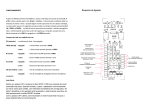
ATOM1
Asynchronous Transfer Mode Microcode for the PowerQUICC
1.
INTRODUCTION
ATOM1 is an MPC860 RAM-based microcode that provides physical layer ATM functions by
converting one or more of the PowerQUICC's serial communication controllers (SCCs) into an
ATM cell transmitter and receiver. ATOM1 provides the user with cell streaming facilities (cell
reception and transmission) and event indications. The user can add AAL functions to ATOM1
using software.
The primary application of ATOM1 is intended to be G.804 plesiochronous digital hierarchy
(PDH) and synchronous digital hierarchy (SDH) E1 and DS1 ATM equipment. Such equipment
is used for signalling and low rate data transfer and may be part of the telecommunications
infrastructure or terminal equipment.
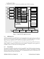
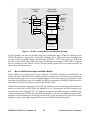
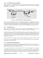
Figure 1 shows an ATM communications module built around the PowerQUICC running an
ATOM1 microcode. This module could be a board within a larger system or part of a larger
ATM board. The ATOM1 microcode runs on the PowerQUICC’s RISC communications
processor (CP) and is stored in the dual port RAM. The user interface to ATOM1 is through
buffer descriptors located in the PowerQUICC’s dual port RAM and data buffers located in
external memory. The PowerQUICC’s PowerPC core controls the module and memory using
the on-chip memory controller and other integration features.
1.1.
Key Features of ATOM1
The key features of ATOM1 are:
• Cell transmission and reception for all AAL protocols.
• Handles serial data rates up to 8 Mbps with a 25 MHz PowerQUICC and up to 16 Mbps
with a 50 MHz PowerQUICC.
• Any or all of the PowerQUICC’s SCCs can simultaneously handle ATM cells.
• Transmit and receive data buffers located in main memory.
• On transmission, ATOM1 constructs the cell header and appends the user defined
payload.
• Bandwidth reservation option in the transmit queue to allow mixing of data and
isochronous services.
• On reception, ATOM1 verifies incoming cell headers and strips the HEC before passing
the cell to the user.
• Automatic empty cell transmission when there are no pending data transfers.
• Receiver filters and discards empty cells and those with non-matching addresses.
• CAM support on reception for handling many connections.
• User controlled cell scrambling option.
• Incoming cells with incorrect HECs are received and marked as such.
• A CRC-32 calculator is available to reduce processor performance requirements when
MPC860 ATOM1 User’s Manual 1.0
-5-
No Restriction on Circulation
handling AAL5 cells.
• Standard PowerQUICC features are available when ATOM1 is running.
E1 ATM
Frame
Relay
UART
E1 ATM Line
Transceiver
E1 ATM Line
Transceiver
Frame
Relay Driver
SCC1
RISC CP
PowerPC Core
Dual Port RAM
SIM
Periodic Timers
14 SDMAs
System
Protection
SCC2
Time Slot Assigner
E1 ATM
SCC3
SCC4
SMC1
SMC2
RS-232
Driver
2 IDMAs
SPI
CPM
4Timers
Clock
Generator
Interrupt
Controller
Memory
Controller
Chip Selects
MPC860
PowerQUICC
System
System
Interface
Boot ROM
DRAMC
SRAMC
32-bit SRAM
32-bit DRAM
Figure 1. Typical ATOM1 Application System
1.2.
MPC860 SCCs
ATOM1 can operate on any MPC860 SCC and can simultaneously operate on any two, three or
all four SCCs. To maintain the performance of ATOM1, it is recommended that the highest
speed connection operates on SCC1 and the lowest speed connection on SCC4.
ATOM1 uses the SCC in transparent mode with microcode performing ATM cell functions.
When ATOM1 is loaded and RAM microcode is enabled, transparent mode operation is
available on any SCC other than ones running ATOM1.
1.3.
Conventions
The reader is assumed to be familiar with the PowerQUICC and ATM. For further information
about the PowerQUICC, please refer to the MPC860 User's Manual. Full details of the ATM
protocols can be found in the relevant ITU-T recommendations and the ATM Forum UNI
document listed at the end of this manual.
MPC860 ATOM1 User’s Manual 1.0
-6-
No Restriction on Circulation
In this manual, the term “user” is used to describe the CPU software that drives ATOM1. In the
MPC860 this is the on-chip PowerPC core.
2.
ATOM1 OPERATION
ATOM1 transmits and receives 53-byte ATM cells as defined in the ATM Forum UNI
specification (ATOM1 also handles NNI cells). Cells are transmitted from a single queue and
the user has full control over each cell’s GFC, VPI, VCI, PT, CLP and payload fields. ATOM1
generates and inserts the cell HEC field on transmission and checks and strips it on reception.
An option is included to apply the HEC coset pattern (binary 01010101) to transmitted and
received cells.
ATOM1 performs cell rate adaptation to the capacity of the transmission link by the inserting
empty cells when no cells are queued by the user. On reception, ATOM1 ignores empty cells.
The user can define the empty cell to be either an unassigned or idle cell.
Received cells with HEC errors are received and marked as such. The HEC is passed to the user
to allow user software to implement HEC correction algorithms as required. ATOM1 does not
attempt to correct any HEC errors.
ATOM1 provides an option to scramble data on transmission and receive scrambled data using
the X43+1 scrambling algorithm. The first cell to be transmitted by ATOM1 after initialisation
will not be correctly scrambled because there is no valid data in the 43-bit delay line. ATOM1
always transmits an empty cell first therefore avoiding data corruption. On reception, the
descrambling algorithm self-synchronises before the HEC delineation process is complete and
cell reception begins.
2.1.
Number of Connections
ATOM1 transmits one cell at a time on the virtual connection specified for that cell. The user
can transmit ATM cells with the whole range of the cell's address field (VCI and VPI combined).
ATOM1 receives cells after matching the cell header with a header look-up table or an external
CAM. The internal look-up table has up to 16 entries and cell headers can have bits masked
before the comparison.
The user must maintain enough open channels to receive OAM and signalling cells. User
software must handle OAM and signalling cells.
2.2.
Cell Delineation
The user must provide synchronisation signals to the PowerQUICC and octet-align incoming
cells to the synchronisation signals. ATOM1 provide SDH/PDH oriented cell delineation using
the HEC mechanism defined in I.432 on an octet basis. The synchronisation signals need not
delimit the start of cell but must be octet aligned with incoming cells. When using E1 and T1
ATM links, the cells are always octet aligned (see ITU G.804) and synchronisation signals are
provided by the E1 and T1 interface devices.
MPC860 ATOM1 User’s Manual 1.0
-7-
No Restriction on Circulation
When reception commences, ATOM1 takes a short while to acquire correct cell delineation.
Once ATOM1 has locked to the incoming cell stream, it remains locked unless there are
excessive errors. An interrupt is generated whenever the cell lock status changes and a status
bit will indicate the current delineation status.
Further details of the cell delineation mechanism are given in Appendix A.
2.3.
AAL Frame Check Sequences
To increase software throughput of AAL5 frames, a CRC-32 calculator is included. This is not
an integral part of the cell transmission and reception process in order that CRC-32 sequences
may be calculated across long AAL5 frames made up of interleaved ATM cells. The CRC-32
calculator is a command which ATOM1 interprets by working through a data buffer generating
the required CRC-32 sequence.
2.4.
PDH & SDH Physical Layer Signalling & OAM Functions
PDH and SDH framing physical layer signalling and OAM functions are not provided by
ATOM1 but the user can handle these by routing the PDH/SDH OAM, signalling and
overhead timeslots to one of the PowerQUICC's SMCs or another SCC.
2.5.
Traffic Control
ATOM1 transmits cells from it's single transmission queue in the order that they are presented.
It is the user's responsibility to apply traffic management techniques to avoid congestion and
breaking the UPC rules if the connection data rate is less than the transmit bit rate. Failure to
apply these techniques may result in bursty traffic on open connections.
When ATOM1's transmit queue is empty, ATOM1 will automatically transmit empty cells.
2.6.
Physical Interface
The ATOM1 microcode is independent of the physical interface standard used. Generally, one
of the PowerQUICC’s TDM ports will be used with ATOM1 to allow easy connection to an E1
or T1 line interface device. Other serial interfaces are not precluded and may be selected when
programming the MPC860 serial interface. This User’s Manual describes the TDM interface
using the Time Slot Assigner (TSA).
2.7.
Buffer Descriptor and Buffer Structures
ATOM1 uses an optimized version of the standard MPC860 data buffer and buffer descriptor
(BD) structures. The ATOM1 structures are better suited to handling numerous small data
buffers as is required in ATM. The BDs are just two bytes long instead of the normal eight byte
BDs and buffers are fixed length. Data buffers are scattered in receive and transmit buffer
memory areas, each 16K bytes, located anywhere in the processor’s memory map.
MPC860 ATOM1 User’s Manual 1.0
-8-
No Restriction on Circulation
3.
REGISTERS
ATOM1 requires several general MPC860 and SCC registers to be configured for operation and
reports status in SCC registers.
3.1.
General Registers
All the MPC860 general registers (SIM, memory controller, chip select, SDMA, etc.) must be
configured as described in the MPC860 User’s Manual with the exception of the CP Control
Registers and RISC Controller Configuration Register. Interrupts are generated by ATOM1 and
the MPC860 interrupt controller must be configured by the user (see the MPC860 User’s
Manual).
3.1.1.
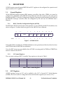
RISC Controller Configuration Register (RCCR)
The MPC860’s RCCR controls microcode operation. To run ATOM1, the RCCR should be set as
shown in Figure 2. Further details are given in the MPC860 User’s Manual.
ATOM1
0
1
TIME
-
0
0
2
7
8
9
TIMEP
EX1M
EX0M
0
0
0
10
11
EX1P
0
0
12
13
EIEE
SCD
0
0
14
15
ERAM
1
0
Figure 2. ATOM1 RCCR
Setting RCCR bit 14 enables the ATOM1 RAM microcode operation and this should not be done
until ATOM1 and the MPC860 are initialized.
Note: the RISC timers are unavailable when ATOM1 is running and the TIME and TIMEP bits
must be cleared in the RCCR.
3.1.2.
CP Control Registers
The user must configure RISC Controller Trap registers as shown in Table 1.
Address
Name
Description
User Writes (hex)
REGB+$5CC
RCTR1
RISC Controller Trap Register 1
8056
REGB+$5CE
RCTR2
RISC Controller Trap Register 2
8076
REGB+$5D0
RCTR3
RISC Controller Trap Register 3
8036
REGB+$5D2
RCTR4
RISC Controller Trap Register 4
8818
Table 1: RISC Control Registers
3.2.
SCC Registers
ATOM1 operates using an SCC and is enabled in the SCC’s General SCC Mode Register
(GSMR). The clock source is configured in the serial interface registers (see section 3.3.1).
MPC860 ATOM1 User’s Manual 1.0
-9-
No Restriction on Circulation
3.2.1.
General SCC Mode Register (GSMR)
ATOM1 requires the following bits to be set in the GSMR: TRX, TTX, CDP, CTSP, CDS and
CTSS. To enable ATOM1’s transmit and receive functions, the ENT and ENR bits must be set
when the initialisation sequence has been completed. Full GSMR details are given in the
MPC860 User’s Manual.
Additionally, the REVD bit in the GSMR (bit 18) changes function to become the CAM control
bit when ATOM1 is running:
CAM
0
1
Use the internal address table for address matching.
Use the external CAM for address matching.
To enable an SCC to run ATOM1, the SCC must be in transparent mode and have MRBLR = 0.
When MRBLR is programmed with a non-zero value, the SCC operates in transparent mode.
Mixed mode operation of an SCC (where the transmitter runs ATOM1 and the receiver is in
transparent mode or vice versa) running ATOM1 is not allowed.
When ATOM1 is loaded and running, the maximum serial performance of an SCC in
transparent mode is reduced very slightly.
3.2.2.
Protocol Specific Mode Register (PSMR)
The SCC Protocol Specific Mode Register (PSMR) controls various SCC functions that are
protocol specific. Before enabling ATOM1, the user should initialize the PSMR. The PSMR
should only be written when the transmitter and receiver are disabled, otherwise erratic
behaviour could result.
For ATOM1, the PSMR is used to control the scrambling and HEC coset functions of both the
transmitter and receiver (see Figure 3).
0
1
2
3
4
5
6
7
8
9
10
11
12
13
14
15
-
-
SCRAM
-
-
-
-
COSET
-
-
-
-
-
-
-
-
Figure 3. ATOM1 PSMR
SCRAM
0
1
Disable cell payload scrambling during transmission and reception.
Enable cell payload scrambling during transmission and reception.
COSET
0
1
Do not apply the HEC coset rules.
Apply the HEC coset to all transmitted and received cells.
3.2.3.
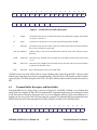
SCC Event Register (SCCE)
The SCC event register (SCCE) contains status bits for events recognized by ATOM1 and the
SCC circuitry. Whenever a bit is set in the SCCE, an interrupt to the user is generated unless the
corresponding bit in the SCC Mask register (SCCM) is set. All bits in the SCCE are sticky bits:
they are set by the SCC hardware or ATOM1 and must be reset by the user writing a one.
MPC860 ATOM1 User’s Manual 1.0
-10-
No Restriction on Circulation
Bits 0-7 are set by the SCC hardware and some unused bits may be set. The user should mask
interrupts from all unused bits in the SCCM. Bits 8-15 are set by ATOM1 to indicate events that
it has detected (see Figure 4).
0
1
2
3
4
5
6
7
8
9
10
11
12
13
14
15
-
-
-
GLR
GLT
DCC
-
-
NMA
SYNC
FIFO
HEC
OAM
BSY
TX
RX
Figure 4. ATOM1 SCCE
RX
A cell has been received and a receive buffer used. This bit is set on completion of reception.
TX
A cell has been transmitted and a transmit buffer used.
BSY
A cell was received and discarded due to lack of receive buffers.
OAM
A control cell (OAM or reserved for future use as indicated by the PT field) been received and a
receive buffer used. This bit is set on completion of reception. When this bit is set, the RX bit is
also set but about 10 system clocks later.
HEC
A cell has been received with a HEC error. This bit is also set when the SYNC bit is set. The HEC
bit is set as soon as a HEC error is detected - it does not wait until the complete cell is received.
FIFO
A transmit FIFO underrun or receive FIFO overrun error has occurred. See ASTATUS for the
exact status.
SYNC
ATOM1 has lost or gained cell delineation.
NMA
ATOM1 received a cell with a non-matching address.
DCC
The carrier sense status as generated by the DPLL has changed. See description of the Transparent
Mode SCCE in the MPC860 User’s Manual.
GLT
A clock glitch was detected by the SCC on the transmit clock. See description of the Transparent
Mode SCCE in the MPC860 User’s Manual.
GLR
A clock glitch was detected by the SCC on the receive clock. See description of the Transparent
Mode SCCE in the MPC860 User’s Manual.
3.2.4.
SCC Mask Register (SCCM)
The SCCM has the same bit definitions as the SCCE and allows the user to mask interrupts.
Further details are given in the MPC860 User’s Manual.
3.2.5.
SCC Status Register (SCCS)
The function of the SCCS register is unchanged when ATOM1 uses an SCC.
3.3.
Serial Interface
ATOM1 may use the MPC860’s serial interface (SI) in any mode although the time division
multiplex mode to allows easy connection to E1 and T1 line interface devices. This section of
MPC860 ATOM1 User’s Manual 1.0
-11-
No Restriction on Circulation
the User’s Manual concentrates on the TDM interface although use of other serial interfaces is
not precluded.
It is the user’s responsibility to ensure that incoming cells are octet aligned with the SI
handshake or synchronisation pulses. ATOM1 will then apply the cell HEC delineation
mechanism correctly and synchronise with the incoming cell stream.
ATOM1 can use either of the MPC860 TDM ports. Programming information is given here for
use of TDM A and can easily be converted for TDM B. Further information about the SI is given
in the MPC860 User’s Manual.
3.3.1.
Serial Interface Registers
The SI registers SIMODE, SIGMR and SICR should be programmed for the required interface
standard and the user must configure the SI RAM pointer (SIRP) as required in the system. An
example of programming the SI registers for connection to a line interface device with common
transmit and receive clocks is shown in Table 2. In this example, ATOM1 is running on SCC1.
Note: the timeslot assigner TSA must not be enabled in SIGMR until the SI RAM and other
registers have been configured.
Register
User Writes (hex)
SIMODE
Serial Interface Mode Register
0000 0058
SIGMR
Serial Interface Global Mode Register
04
SICR
Serial Interface Clock Route Register
0000 0040
Table 2: MPC860 Serial Interface Programming Example
3.3.2.
Serial Interface RAM
ATOM1 can use the MPC860 TSA with independent receiver and transmitter routing RAM
tables. An example of programming these two tables for back-to-back ATM cell transmission
and reception is given in Table 3. TDM A is used and data is routed to SCC1. Other SCCs and
TDM B may be used. For debug purposes, all four SI strobes are asserted during various
timeslots: L1ST1 during cell header transmission, L1ST2 on HEC transmission, L1ST3 during
cell header reception and L1ST4 on HEC reception.
SI RAM Entry
User Writes (hex)
Strobe Asserted
Remarks
Rx A 0
104E
L1ST3
Rx A 1
2042
L1ST4
Rx A 2
007E
-
Receive first sixteen bytes of cell payload
Rx A 3
007E
-
Receive second sixteen bytes of cell payload
Rx A 4
007F
-
Receive final sixteen bytes of cell payload
Tx A 0
044E
L1ST1
Transmit four bytes of cell header
Tx A 1
0842
L1ST2
Transmit one byte HEC field
Receive four bytes of cell header
Receive one byte HEC field
Table 3: Serial Interface RAM Programming Example
MPC860 ATOM1 User’s Manual 1.0
-12-
No Restriction on Circulation
SI RAM Entry
User Writes (hex)
Strobe Asserted
Tx A 2
007E
-
Transmit first sixteen bytes of cell payload
Remarks
Tx A 3
007E
-
Transmit second sixteen bytes of cell payload
Tx A 4
007F
-
Transmit final sixteen bytes of cell payload
Table 3: Serial Interface RAM Programming Example
3.4.
Parallel Port Registers
For ATOM1 operation over TDM A, the MPC860 parallel port pins should be set up to interface
to external signals as shown in Table 4. The TSA strobes and SDMA Acknowledge pins are
shown and common receive and transmit clocks are used.
Signal
Pin
Direction
L1TXDA
PA9
Output
L1RXDA
PA8
Input
L1RSYNCA
PC4
Input
L1RCLKA
PA7
Input
L1ST1
PB19
Output
L1ST2
PB18
Output
L1ST3
PB17
Output
L1ST4
PB16
Output
SDACK1*
PC5
Output
SDACK2*
PC7
Output
Table 4: ATOM1 TDM A Port Pin Requirements
To achieve this, Table 5 shows an example of how the port registers may be programmed.
Register
User Writes (hex)
PIP Configuration Register
0000
PADIR
Port A Data Direction Register
00C1
PAPAR
Port A Pin Assignment Register
01C0
PAODR
Port A Open Drain Register
0000
PBDIR
Port B Data Direction Register
0000 0000
PBPAR
Port B Pin Assignment Register
0000 F000
PBODR
Port B Open Drain Register
0000
PCDIR
Port C Data Direction Register
0500
PCPAR
Port C Pin Assignment Register
0D00
PCSO
Port C Special Option Register
0000
PCINT
Port C Interrupt Control Register
0000
PIPC
Table 5: MPC860 Port Register Programming
MPC860 ATOM1 User’s Manual 1.0
-13-
No Restriction on Circulation
4.
ATOM1 SCC PARAMETER RAM
When ATOM1 operates on a particular SCC, the SCC parameter RAM memory map is that
shown in Table 6. The user must initialize the parameter RAM with the values given after reset
or when re-initializing ATOM1.
Address
Name
Width
Description
User Writes (hex)
SCC Base + 00
RBASE
Halfword
Receive BD Base Address
UD
SCC Base + 02
TBASE
Halfword
Transmit BD Base Address
UD
SCC Base + 04
RFCR
Byte
Receive Function Code
UD
SCC Base + 05
TFCR
Byte
Transmit Function Code
UD
SCC Base + 06
MRBLR
Halfword
SCC Base + 08
RSTATE
Word
Receiver Internal State
SCC Base + 0C
R_PTR
Word
Receiver Internal Data Pointer
SCC Base + 10
RBD_PTR
Halfword
Receive BD Pointer
SCC Base + 12
R_CNT
Halfword
Receive Internal Byte Counter
-
SCC Base + 14
RTEMP
Word
Receiver Temporary Data Storage
-
SCC Base + 18
TSTATE
Word
Transmitter Internal State
SCC Base + 1C
T_PTR
Word
Transmit Internal Data Pointer
Transparent Rx Max Buffer Length
0000
use init rx/tx
command
use init rx/tx
command
use init rx/tx
command
use init rx/tx
command
SCC Base + 20
TBD_PTR
Halfword
Transmit BD Pointer
SCC Base + 22
T_CNT
Halfword
Transmit Internal Byte Counter
SCC Base + 24
TTEMP
Word
Transmitter Temporary Data Storage
-
SCC Base + 28
ALPHA
Halfword
Receiver Delineation Alpha Counter
-
SCC Base + 2A
DELTA
Halfword
Receiver Delineation Delta Counter
-
SCC Base + 2C
AVERSION
Halfword
ATOM1 Version Number
-
SCC Base + 2E
CAM_PORT
Halfword
SCC Base + 30
RX_BUFF1
Word
Receive Buffer Area Start Address
UD
SCC Base + 34
TX_BUFF1
Word
Transmit Buffer Area Start Address
UD
SCC Base + 38
EHEAD
Word
Empty Cell Header
(little endian byte format)
0000 0000
or 0100 0000
SCC Base + 3C
EPAYLOAD
Word
Empty Cell Payload
(little endian byte format)
6A6A 6A6A
SCC Base + 40
RSTUFF
Word
Receive Data Stuffing Location (53
to 52 byte conversion)
SCC Base + 44
SHUFFLESTATE
Halfword
Receiver Data Shuffling State
SCC Base + 46
RHECTEMP
Halfword
Temporary HEC Storage
-
SCC Base + 48
THECTEMP
Halfword
Temporary HEC storage area
-
SCC Base + 4A
ASTATUS
Halfword
ATOM1 status halfword
SCC Base + 4C
NMA_HEAD
Word
Non-Matching Address Cell Header
-
SCC Base + 50
NMA_CNT
Halfword
Non-Matching Address Cell Counter
0000
SCC Base + 52
HEC_ERR
Halfword
HEC Error Counter
0000
CAM Port B Mask
-
-
0000
0000
Table 6: ATOM1 SCC Parameter RAM Memory Map
MPC860 ATOM1 User’s Manual 1.0
-14-
No Restriction on Circulation
Address
Name
Width
SCC Base + 54
RSCRAM
Word
SCC Base + 58
RSCRAM1
Word
SCC Base + 5C
TSCRAM
Word
Description
User Writes (hex)
Receiver Scrambling Storage
Transmitter Scrambling Storage
-
SCC Base + 60
TSCRAM1
Word
SCC Base + 64
HEADMASK
Word
Cell Header Comparison Mask
UD
-
SCC Base + 68
HEAD1
Word
Cell Header Look-Up Table Entry 1
UD
SCC Base + 6C
HEAD2
Word
Cell Header Look-Up Table Entry 2
UD
SCC Base + 70
HEAD3
Word
Cell Header Look-Up Table Entry 3
UD
SCC Base + 74
HEAD4
Word
Cell Header Look-Up Table Entry 4
UD
SCC Base + 78
HEAD5
Word
Cell Header Look-Up Table Entry 5
UD
SCC Base + 7C
HEAD6
Word
Cell Header Look-Up Table Entry 6
UD
SCC Base + 80
HEAD7
Word
Cell Header Look-Up Table Entry 7
UD
SCC Base + 84
HEAD8
Word
Cell Header Look-Up Table Entry 8
UD
SCC Base + 88
HEAD9
Word
Cell Header Look-Up Table Entry 9
UD
SCC Base + 8C
HEAD10
Word
Cell Header Look-Up Table Entry 10
UD
SCC Base + 90
HEAD11
Word
Cell Header Look-Up Table Entry 11
UD
SCC Base + 94
HEAD12
Word
Cell Header Look-Up Table Entry 12
UD
SCC Base + 98
HEAD13
Word
Cell Header Look-Up Table Entry 13
UD
SCC Base + 9C
HEAD14
Word
Cell Header Look-Up Table Entry 14
UD
SCC Base + A0
HEAD15
Word
Cell Header Look-Up Table Entry 15
UD
SCC Base + A4
HEAD16
Word
Cell Header Look-Up Table Entry 16
UD
UD = User Defined
Table 6: ATOM1 SCC Parameter RAM Memory Map
4.0.1.
BD Queue Pointers (RBASE and TBASE)
The user configures RBASE and TBASE to define the starting location of the receive and
transmit BD queues in the dual-port RAM. Further information is given in the MPC860 User’s
Manual.
4.0.2.
SCC Function Code Registers (RFCR and TFCR)
The user configures RFCR and TFCR to define the SDMA function code pin settings during
SDMA transfers. Further information is given in the MPC860 User’s Manual.
4.0.3.
Transparent Mode Receive Maximum Buffer Length (MRBLR)
To run ATOM1 on an SCC, the user must program that SCC’s MRBLR to zero. When MRBLR
is programmed with a non-zero value, the SCC operates in transparent mode as described in
the MPC860 User’s Manual.
4.0.4.
SCC Internal State Parameters (RSTATE and TSTATE)
ATOM1 uses RSTATE and TSTATE to store internal state variables and flags during operation.
The user must not write to these locations.
MPC860 ATOM1 User’s Manual 1.0
-15-
No Restriction on Circulation
4.0.5.
BD and Buffer Pointers (R_PTR, RBD_PTR, T_PTR and TBD_PTR)
During cell transmission and reception, ATOM1 uses R_PTR, RBD_PTR, T_PTR and TBD_PTR
as pointers to the current BD and data locations. RBD_PTR and TBD_PTR point to the current
or next BD to use and need to be initialized with the Init Rx/Tx command to point to the
locations given in RBASE and TBASE. R_PTR, and T_PTR point to the next data location in
memory. When ATOM1 is operating, these locations should not be written by the user. Further
information is given in the MPC860 User’s Manual.
4.0.6.
Transmit and Receive Buffer Queue Start Pointers (TX_BUFF1, RX_BUFF1)
The user configures TX_BUFF1 and RX_BUFF1 to define the starting location of the transmit
and receive buffer areas in main memory. This is the starting address of the 16K byte areas
where transmit and receive buffers reside. TX_BUFF1 and RX_BUFF1 must be word aligned
addresses (bits 31 and 30 must be zero).
TX_BUFF1 and RX_BUFF1 can be dynamically changed provided that care is taken to
synchronise the buffer queues held in user software and the queues that the PowerQUICC’s CP
sees. The CPM reads TX_BUFF1 and RX_BUFF1 every time that it opens a data buffer so it is
advised that the transmit and receive queues are allowed to empty before TX_BUFF1 and
RX_BUFF1 are changed.
4.0.7.
Buffer Counters (R_CNT and T_CNT)
During ATM cell transmission and reception, ATOM1 uses R_CNT and T_CNT to count the
number of bytes transmitter or received. The user must not write to these locations.
4.0.8.
Receiver Delineation Counters (ALPHA and DELTA)
ATOM1 applies the HEC delineation mechanism described in I.432 with Alpha=7 and Delta=6
to locate and maintain cell synchronisation. During reception, ATOM1 updates the ALPHA
and DELTA parameter locations and the user must not write to these locations. There is no need
to initialise these locations.
4.0.9.
Version Number (AVERSION)
During operation, ATOM1 writes a version number to AVERSION. The current version
number of ATOM1 on the PowerQUICC stored in AVERSION is $0081.
4.0.10.
CAM Port Selection (CAM_PORT)
When the CAM interface is enabled, the user should set one or more bits in CAM_PORT to
select which of the PowerQUICC’s Port B pins is the match input or inputs for this SCC.
CAM_PORT is a 16-bit parameter where bit 15 of CAM_PORT corresponds to PB31, bit 15 to
PB30, etc. as shown below:
0
1
2
3
4
5
6
7
8
9
10
11
12
13
14
15
PB16
PB17
PB18
PB19
PB20
PB21
PB22
PB23
PB24
PB25
PB26
PB27
PB28
PB29
PB30
PB31
MPC860 ATOM1 User’s Manual 1.0
-16-
No Restriction on Circulation
4.0.11.
Empty Cell Data (EHEAD and EPAYLOAD)
ATOM1 transmits and receives empty cells using EHEAD and EPAYLOAD. On transmission,
an empty cell is made up by transmitting EHEAD once, calculating and transmitting a HEC and
transmitting EPAYLOAD twelve times. On reception, the incoming header is compared with
EHEAD to check for empty cells and EPAYLOAD is not used.
The user is free to select whatever empty cell header and payload values are required: the ATM
Forum UNI Specification states that unassigned cells should be transmitted while the ITU
mandates use of idle cells.
The user must write the EHEAD and EPAYLOAD parameters as required and these two
locations must be written in little endian byte order. Unassigned cells are used as empty cells
when EHEAD = $0000 0000 and idle cells when EHEAD = $0100 0000. In both cases,
EPAYLOAD should be initialised to $6A6A 6A6A.
4.0.12.
Status Information (ASTATUS)
The ATOM1 Status parameter provides the user with additional status information concerning
FIFO errors and receiver synchronisation status. ASTATUS is shown in Figure 5.
0
1
2
3
4
5
6
7
8
9
10
11
12
13
14
15
-
-
-
-
-
-
ORUN
URUN
-
-
-
-
-
-
-
LOCK
Figure 5. ASTATUS
Bits in the upper byte is set by ATOM1 and cleared by the user. Bits in the lower byte are set
and cleared by ATOM1. During initialisation, the user must clear all bits in ASTATUS. During
operation, the user can read and clear (write zero) to the upper byte but must only read the
lower byte.
FIFO overruns and underruns are reported in the SCCE FIFO bit and further information is
given in the ORUN and URUN bits:
ORUN
0
1
No Receiver FIFO Overrun.
Receiver FIFO Overrun.
URUN
0
1
No transmitter FIFO underrun.
Transmitter FIFO underrun.
Each change in state of the receiver cell delineation is reported in the SCCE SYNC bit. The
LOCK bit shows the current delineation status:
LOCK
4.0.13.
0
1
The ATOM1 receiver is out of synchronisation and is not receiving cells.
The ATOM1 receiver has gained cell delineation and is receiving cells.
Non-Matching Header Storage and Counter (NMA_HEAD and NMA_CNT)
When a cell is received with a non-matching header, the header (minus the HEC) is written to
NMA_HEAD, NMA_CNT is incremented and the NMA bit set in the SCCE. NMA_HEAD is a
MPC860 ATOM1 User’s Manual 1.0
-17-
No Restriction on Circulation
location where headers from non-matching cells are logged and NMA_CNT is a counter of nonmatching cells. The user is free to read and clear NMA_CNT at any time.
4.0.14.
HEC Error Counter (HEC_ERR)
HEC_ERR is a 16-bit counter of incoming cells with HEC errors. The user is free to read and
clear HEC_ERR at any time.
4.0.15.
Incoming Header Mask and Look-up Table (HEADMASK and HEADn)
When the CAM option is disabled, ATOM1 masks the header of each incoming cell with
HEADMASK and then searches for the result in the HEADn table. When a match is found, the
cell is received otherwise the cell header is logged in NMA_HEAD and the remainder of the cell
is discarded.
The HEADMASK masking process uses a bitwise AND function so bits can be masked out by
clearing the relevant bit in HEADMASK. The bit locations for HEADMASK are shown in
Figure 6. Bit 31 must always be written with zero.
0
3
4
GFC
11
12
VPI
27
28
VCI
30
PT
31
0
Figure 6. HEADMASK
The result of the masking is then compared with each of the HEADn values, starting with
HEAD1. Although sixteen locations are shown in the HEADn table, the user may define fewer.
The final location in the table is denoted with the Last bit being set. When multiple HEADn
locations are being used, the user should take care because the look-up table can overlap other
peripheral areas in memory (see the MPC860 User’s Manual for further details). If the look-up
table is extended to overlap other peripheral’s parameter RAM areas, the other peripherals
cannot be used.
The bit locations for the HEADn locations are shown in Figure 7. Bit 31 should be written with
zero except for the last entry in the table.
0
3
GFC
4
11
12
VPI
27
VCI
28
30
PT
31
Last
Figure 7. HEADn
ATOM1 searches the HEADn table sequentially so the headers for the most frequently
connections should be at the beginning of the table.
4.0.16.
Temporary Data Storage
During ATM cell transmission and reception, ATOM1 uses RTEMP, TTEMP, RSTUFF,
RHECTEMP, THECTEMP, RSCRAM, RSCRAM1, TSCRAM and TSCRAM1 to store temporary
data. This data is for internal use and the user must not write to these locations.
MPC860 ATOM1 User’s Manual 1.0
-18-
No Restriction on Circulation
5.
ATOM1 COMMANDS
The following commands are understood by ATOM1:
•
•
•
•
•
•
•
Initialise Receiver and Transmitter Parameters
Initialise Receiver Parameters
Initialise Transmitter Parameters
Stop Transmit
Restart Transmit
Restart Reception
CRC-32 Calculator
Execution of other SCC commands may cause errant behaviour. All commands are given
through the Command Register and operate as with other protocols except Restart Reception.
The ATOM1 commands to initialise the receiver and transmitter parameters operate the same
as for other SCC protocols. If the initialisation commands are given during cell transmission
and reception, cell synchronisation will be lost.
The Stop Transmit Command stops cell transmission immediately and the transmit line goes
high. To stop transmission of data cells but continue with empty cells, the user must wait for
the transmit BD queue to empty.
The commands are run by writing the command and channel number to the PowerQUICC’s
Command Register (CR). The op-codes for the initialisation, Stop Transmit and Restart
Transmit command are the same as for the PowerQUICC’s other protocols. The op-code for the
Restart Reception command is and the CRC-32 calculator 1111. All other bits in the CR remain
unchanged.
Command execution latency for the initialisation, Stop Transmit and Restart Transmit
command are the same as for the PowerQUICC’s other protocols. The Restart Reception
command is executed when the current cell being received is complete and execution time
therefore depends on the data rate and when the command is given. For all commands, ATOM1
clears the FLG bit in the CR to indicate completion of the command.
5.1.
Restart Reception Command
The Restart Reception Command is similar to Enter Hunt Mode. If ATOM1 is currently
receiving an empty cell, cell delineation is immediately lost and the resynchronisation process
begins. If the current cell being received is a data or control cell (being received or discarded by
ATOM1), the current buffer is closed and cell delineation is lost at the end of the cell. The Enter
Hunt Mode command should not be used with ATOM1.
To restart the receiver immediately regardless of the current state, the Init Rx Parameter
command can be used.
MPC860 ATOM1 User’s Manual 1.0
-19-
No Restriction on Circulation
The Restart Reception Command and the CRC-32 Calculator share the same op-code in the
command register. To issue a Restart Reception Command, the user must ensure that the
current CRC-32 calculation is complete and the CRC_CNT parameter is zero.
5.2.
CRC-32 Calculator
The CRC-32 Calculator command calculates the 32-bit CRC sequence used in AAL5 frames on
a data buffer defined by a pointer and length. Multiple buffers may be strung together by the
user to calculate the CRC-32 value over a large AAL5 frame made up of multiple CRC-32
buffers. ITU I.363 gives more details and examples of AAL5 CRC calculations.
Note: The PowerQUICC’s CP runs the ATOM1 CRC-32 calculator as its lowest priority task.
High traffic throughput on the SCCs and other CP activity will adversely affect the CRC-32
calculator’s performance.
The ATOM1 CRC-32 calculator replaces four parameters in PowerQUICC’s RISC Timer
Parameter RAM area (starting at DPRBASE + $DB0) as shown in Table 7. The user must
initialize the CRC-32 parameter RAM with the values given after reset or when re-initializing
ATOM1.
Address
Name
Width
Description
User Writes (hex)
DPRBASE + $DB0
CRC_PTR
Word
CRC-32 Calculator Pointer
UD
DPRBASE + $DB4
CRC_CNT
Halfword
CRC-32 Calculator Counter
UD
DPRBASE + $DB6
CRC_FC
Byte
CRC-32 Calculator Function Code
UD
DPRBASE + $DB8
CRC_RESULT
Word
CRC-32 Calculator Seed Value and
Result
0000 0000 or UD
UD = User Defined
Table 7: ATOM1 CRC-32 Calculator Parameter RAM Memory Map
To start a CRC-32 calculation, the CRC_PTR, CRC_CNT, CRC_RESULT and CRC_FC
parameters must be initialised to give the start address of the data block for the calculation,
block length, starting CRC-32 seed and function code. ATOM1 reads and writes these four
parameters during a CRC-32 calculation so they must not be altered by the user while the
calculation is in progress.
The CRC_PTR may be programmed with any address that corresponds to the start of the CRC32 buffer in memory. The length of the buffer must be programmed into the CRC_CNT
parameter. If CRC_CNT is zero at the start of the command, ATOM1 will run a Restart
Reception command rather than the CRC-32 calculator.
The CRC_RESULT parameter must be preset to zero at the start of a new CRC-32 calculation.
On completion of the calculation, CRC_RESULT holds the resulting 32-bit CRC value. At the
beginning of a CRC-32 calculation, CRC_RESULT may be programmed with the result of a
previous CRC-32 calculation if buffers are being strung together.
The user configures CRC_FC to define the SDMA function code pin settings when the SDMA
reads the CRC-32 buffer. Further information is given in the MPC860 User’s Manual.
MPC860 ATOM1 User’s Manual 1.0
-20-
No Restriction on Circulation
A CRC-32 calculation is started by writing $0F01 to the command register. When the command
has been accepted and CRC-32 processing begins, ATOM1 clears the FLG bit in the command
register. Processing continues through the whole CRC-32 buffer and when the calculation is
complete, ATOM1 sets bit 0 in the RISC Timer Even Register (RTER). This can be used to
generate a processor interrupt by programming the PowerQUICC’s interrupt controller. Bit 0
of the RTER should be cleared before a CRC-32 calculation is started.
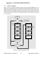
6.
BUFFER DESCRIPTORS & BUFFERS
ATOM1 uses a modified version of the standard MPC860 BD and buffer data structure better
suited to the high number of and small size of ATM cells. There is a single transmit BD queue
and a single receive queue. Associated with each BD queue is a buffer queue. All ATOM1 BDs
are two bytes long and buffers are all 52 bytes long. These BD and buffer sizes maximise the
number of BDs that can be located in the PowerQUICC’s dual port RAM when the ATOM1
microcode is also present and running.
The BDs are a subset of the standard PowerQUICC BDs containing only a 16-bit status and
control halfword. Buffer length and pointer fields are not implemented as for other
PowerQUICC serial protocols. BDs are located in the PowerQUICC’s dual port RAM.
All data buffers have a fixed length of 52 bytes and are located within 16K byte buffer areas in
memory. Receive BD1 is associated with buffer 1, receive BD2 with buffer 2, etc. Transmit and
receive buffers are scattered within a 16K byte memory area and use an eleven bit pointer
within the transmit BD to locate the buffer exactly. The transmitter and receiver each use
different 16K byte buffer areas which may be located anywhere in memory.
6.1.
ATOM1 Buffer Descriptor and Buffer Queues
Figure 8 shows an example of the transmitter BD and data buffer queues and the pointers
associated with them. In this example, there are 20 BDs, each linked to a buffer. TBASE points
to the start of the BD queue and TX_BUFF1 points to the start of the buffer area. ATOM1
calculates the exact start address of a transmit buffer by adding TX_BUFF1 to the address field
in the transmit BD. Buffers may thus be scattered randomly throughout the 16K byte area.
MPC860 ATOM1 User’s Manual 1.0
-21-
No Restriction on Circulation
.
Queue of 20
Tx BDs
Queue of 20
Transmit Buffers
TX_BUFF1
TBASE
TBD_PTR
Tx Buffer 1
Tx BD 1
Tx BD 2
Tx BD 3
Address
Offset in
Tx BD 2
Tx Buffer 2
Tx Buffer 3
T_CNT
T_PTR
Tx BD 19
Tx BD 20
Tx Buffer 20
Tx Buffer 19
16K Byte
Buffer Area
Figure 8. ATOM1 Transmit Buffer and BD Queue Example
In this example, the first two buffers have been transmitted and ATOM1 has advanced the
TBD_PTR pointer to point at the current BD. Similarly, the T_PTR pointer has been advanced
to point to the current data being transmitted by ATOM1. T_CNT is the offset of T_PTR from
the start of the data buffer. When the end of the BD queue is reached, TBD_PTR is wrapped
back by loading it from TBASE. Receive BD and buffer queues follow the same structure as
shown here for transmission.
6.2.
Receive Buffer Descriptor and Data Buffer
Receive BDs are two bytes long as shown in Figure 9. Each BD is linked to one buffer that can
hold a received ATM cell. Receive buffers may be scattered around a 16K byte area of memory
but each buffer must start on a word aligned address. If the start address of a buffer is at the
very end of the 16K byte area (for example, the BD is programmed with $8FFF) then the end of
the received cell will be 48 bytes outside of the 16K byte area.
When the user prepares an empty receive BD, the address pointer to the start of the data buffer
must be written into the BD. When the Empty bit is set, ownership if the BD is handed over
from the user to the PowerQUICC’s CP and the user must not modify any part of the BD. Once
a cell is received and ATOM1 returns the BD and buffer to the user, the address pointer field is
replaced with OAM and error status flags and the HEC of the incoming cell. User software must
maintain a copy of the address pointer for each receive BD in the receive queue.
MPC860 ATOM1 User’s Manual 1.0
-22-
No Restriction on Circulation
0
1
2
3
4
5
6
7
8
9
10
11
12
13
14
15
E
-
W
I
A18
A19
A20
A21
A22
A23
A24
A25
A26
A27
A28
A29
Empty Receive BD as Written by User
E
-
W
I
-
-
OAM
ERR
HEC
Used Receive BD after reception of a Cell
Figure 9. ATOM1 Receive Buffer Descriptor
E
Empty
Control bit set by the user to indicate that the associated buffer is empty and ATOM1
can receive a cell into it.
W
Wrap
Control bit set by the user to wrap the receive BD queue after this BD.
I
Interrupt
Control bit set by the user. When a cell is received into the buffer associated with this
BD, a receive interrupt is generated.
A18-A29 Address
Address offset to the start of the data buffer from the start of the 16K byte receive
data area.
OAM
OAM Cell
Status bit set by ATOM1. The associated cell is an OAM or reserved cell (cell PT field
= 1xx).
ERR
HEC Error Status bit set by ATOM1. The associated cell was received with an error in the header
as detected by the HEC check.
HEC
HEC Byte
Byte containing the received cell’s HEC field.
ATOM1 stores received ATM cells in receive buffers after removing the HEC. Receive data
buffers have the same structure as transmit buffers. The first byte of the buffer is the first byte
received (the GFC field and part of the VPI). The HEC field is removed and stored in the receive
BD.
6.3.
Transmit Buffer Descriptor and Data Buffer
Transmit BDs are two bytes long as shown in Figure 10. Each BD is linked to one buffer that
must hold the complete ATM cell to be transmitted. Transmit buffers may be scattered around
a 16K byte area of memory but must start on a word aligned address. If the start address of a
buffer is at the very end of the 16K byte area (for example, the transmit BD is programmed with
$8FFF) then the end of the transmit cell will be 48 bytes outside of the 16K byte area.
0
1
2
3
4
5
6
7
8
9
10
11
12
13
14
15
R
SKIP
W
I
A18
A19
A20
A21
A22
A23
A24
A25
A26
A27
A28
A29
Figure 10. ATOM1 Transmit Buffer Descriptor
MPC860 ATOM1 User’s Manual 1.0
-23-
No Restriction on Circulation
R
Ready
Control bit set by the user to initiate transmission of the associated cell. ATOM1
clears the Ready bit when the associated buffer has been transmitted.
SKIP
Skip BD
Control bit set by the user. When ATOM1 encounters a transmit BD with the Skip bit
set, an empty cell is transmitted and control passes to the next BD. When the Skip bit
is set, the Ready bit is ignored.
W
Wrap
Control bit set by the user to wrap the transmit BD queue after this BD.
I
Interrupt
Control bit set by the user. When the cell associated with this BD is transmitted, a
transmit interrupt is generated. This bit is ignored when the Skip bit is also set.
A18-A29 Address
Address offset to the start of the data buffer from the start of the 16K byte transmit
data area.
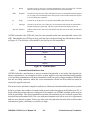
ATOM1 transmits the ATM cell stored in the transmit buffer and automatically inserts the
HEC. Data buffers are all 52 bytes long with the first four bytes being the cell header as shown
in Figure 11. The first byte of the buffer is the first byte to be transmitted.
GFC
VPI
VCI
PT
CLP
Payload
Payload
Payload
Figure 11. Transmit Buffer
6.3.1.
Transmit Bandwidth Reservation
ATOM1 includes a mechanism to reserve transmit bandwidth to aid tasks that require low
latency transmission. An example of such a system might be one that simultaneously handles
voice and data transmissions: the data transmission task can queue a large number of ATM cells
that are not delay sensitive while the voice transmission circuit has less traffic but must be
serviced at regular intervals.
The mixed voice and data example is used here to illustrate the bandwidth reservation system.
In most systems, the number of transmit and receive buffer descriptors and buffers per SCC is
fixed when the system software is designed. For example, the ATOM1 transmit queue may be
fixed at ten buffers. The data transmission software can maintain its own software queue that
may hold several hundred cells. The voice task must transmit each cell as soon as it is generated
and not store them in a queue. If the voice cells were to be placed at the end of the software data
transmission queue, the latency would be too high.
MPC860 ATOM1 User’s Manual 1.0
-24-
No Restriction on Circulation
The transmit bandwidth reservation system avoids this problem by allowing selected BDs to be
reserved for the voice transmission. When ten BDs are allocated to the data and voice
transmission software tasks, nine can be assigned for data and one for voice. This reserves 10%
of the transmission bandwidth for voice channels.
The reservation mechanism uses the Skip bit in the transmit BD. As ATOM1 processes the
transmit BD queue, it transmits cells where the Skip bit is zero. When a BD with the Skip is
encountered, it is skipped and an empty cell is transmitted in its place.
In the mixed data and voice example, the data transmission software can control nine of the ten
BDs and set their Ready bits to initiate transmission. The voice transmission software reserves
one BD by setting its Skip bit. When a voice cell is ready for transmission, the voice transmission
software inserts the header and payload in the relevant transmit data buffer, clears the Skip bit
and sets the Ready bit. Next time that ATOM1 checks this BD, it will see only the Ready bit set
and therefore transmit the voice cell.
Figure 12 illustrates this example. The tenth transmit BD is reserved for voice traffic. While the
voice transmission task is constructing an ATM cell and has nothing in the transmit BD queue,
it reserves bandwidth by setting the Skip bit. When the voice cell has been constructed and
loaded into the tenth transmit buffer, the Skip bit is cleared and the Ready bit set. The voice cell
is then transmitted with a maximum delay of nine cells.
Data Tx Task
Incoming Data
Traffic (Bursty)
Incoming Voice
Traffic (Regular)
Data
Transmission
Task Controls
Nine BDs
Internal Data
Transmission
Queue
Voice Tx Task
Single Cell for
Transmission
Voice
Transmission
Task Controls
One BD
Queue of
10 Tx BDs
Tx BD 1
Tx BD 2
Tx BD 3
Tx BD 4
Tx BD 5
Tx BD 6
Tx BD 7
Tx BD 8
Tx BD 9
Tx BD 10
Figure 12. Mixed Voice and Data Transmission Example
MPC860 ATOM1 User’s Manual 1.0
-25-
No Restriction on Circulation
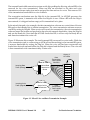
7.
ATOM1 CAM INTERFACE
Figure 13 shows the ATOM1 CAM interface and a timing diagram illustrating operation.
Operation is similar to the Ethernet CAM interface (see the MPC860 User’s Manual for further
details). The SDACK1* signal delimits a header write cycle on the data bus and SDACK2*
delimits payload write cycles. Both SDACK1* and SDACK2* are asserted during the final
payload write cycle. ATOM1 samples the MATCH* signal during the last data transfer of the
cell.
E1 ATM
TSA
SCC
SDMA
RAM
MPC860
PowerQUICC
MATCH*
PowerPC Core
SDACK1* &
SDACK2*
CAM
FC(3:0)
CAM Control
Logic
SDMA Bus Write Cycle
4 Byte
Header
48 Bytes Payload
SDACK1* Output Signal
SDACK2* Output Signal
MATCH* Input Signal
Figure 13. ATOM1 CAM Interface
The user selects the pin to be used as the MATCH* input from the port B PB31-PB16 pins using
the CAM_PORT parameter. Multiple CAMs can be connected to a single SCC running ATOM1
by using multiple MATCH* inputs. ATOM1 looks for one or more of the MATCH* inputs to be
active. The port B pins being used as the MATCH* input must be configured as input ports
using the port B configuration registers PBPAR and PBDIR.
MPC860 ATOM1 User’s Manual 1.0
-26-
No Restriction on Circulation
When ATOM1 is operating on several SCCs concurrently, each may be connected to a CAM. To
distinguish between the SDMA cycles for each SCC, each receiver function codes should be
programmed to a different value.
When the CAM interface is operating with ATOM1, the Ethernet CAM interface can still be
used. The CAM control logic will need to check the function codes and SDACK signals to
determine which SCC has initiated a particular bus cycle and enable the appropriate CAM chip.
8.
LOADING & CONFIGURING ATOM1
Before operation, the ATOM1 microcode must be loaded into the MPC860’s internal RAM. The
microcode is delivered in a file of S-records ready to download to a Motorola 860ADS board
and a general PowerPC assembly code file. Further details of 860ADS download procedures are
given in the 860ADS User’s Manual.
The ATOM1 microcode occupies the internal RAM blocks DPRBASE+2000 to DPRBASE+23FF
and DPRBASE+2F00 to DPRBASE+2FFF. These areas are unavailable for use by the user.
Once the ATOM1 microcode is loaded into the MPC860’s internal RAM, it is initialized as
follows:
1.
2.
3.
4.
5.
6.
7.
Configure SDMA.
Configure parallel ports.
Configure serial interface.
Enable TSA.
Configure CP registers.
Enable RAM microcode.
Configure SCC registers. Configure GSMR, PSMR, SCCE and SCCM to select required
operation.
8. Configure ATOM1 parameter RAM.
9. Initialize queue of empty receive BDs and buffers.
10. Clear transmit BDs.
11. Enable SCC by setting ENT and ENR bits in the GSMR lower word.
Once initialisation is complete, ATOM1 can be controlled through the transmit and receive BD
queues and commands.
Example source code for initialisation and operation of ATOM1 is given in Appendix B.
9.
PERFORMANCE
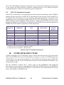
Tables 8 and 9 show the results of some performance characterisation experiments where
ATOM1 is run concurrently with other SCCs. All results are for zero wait state access to
memory. In the experiments, all SCCs were continually transmitting and receiving data cells
(no commands or CRC-32 calculations) and frames of the following size:
MPC860 ATOM1 User’s Manual 1.0
-27-
No Restriction on Circulation
HDLC frames
Ethernet frames
ATM cells
Configuration
24 bytes data + 2 bytes CRC
64 bytes data + 4 bytes CRC
5 byte header + 48 bytes payload
ATOM1 SCCs
Mode
Frequency Ratio
1 ATM
SCC1
ATOM1 - No Scrambling
1:3
1 ATM
SCC1
ATOM1 - Scrambling
1:4.5
2 ATM
SCC1, 2
ATOM1 - No Scrambling
1:8
2 ATM
SCC1, 2
ATOM1 - Scrambling
1:10
3 ATM
SCC1, 2, 3
ATOM1 - No Scrambling
1:10
3 ATM
SCC1, 2, 3
ATOM1 - Scrambling
1:14
4 ATM
SCC1, 2, 3, 4
ATOM1 - No Scrambling
1:13
4 ATM
SCC1, 2, 3, 4
ATOM1 - Scrambling
1:19
System
Frequency
25/40/50
MHz
Table 8: ATOM1 Performance
MPC860 ATOM1 User’s Manual 1.0
-28-
No Restriction on Circulation
ATOM1 SCC
Configuration
Other SCCs
SCC
Mode
Frequency
Ratio
SCC1
ATOM1
No Scrambling
1:12
(note 1)
SCC2/3/4
HDLC
1:8
SCC1
ATOM1
Scrambling
1:12
(note 1)
SCC2/3/4
HDLC
1:9
SCC1
ATOM1
No Scrambling
1:3.5
SCC2/3/4
HDLC
1:390
(note 2)
SCC1
ATOM1
Scrambling
1:5
SCC2/3/4
HDLC
1:390
(note 2)
1 ATM +
1 Ethernet
channel
SCC1
ATOM1
No Scrambling
1:6
SCC2
Ethernet
1:2.5
SCC1
ATOM1
Scrambling
1:7
SCC2
Ethernet
1:2.5
1 ATM,
1 Ethernet +
1 HDLC
channel
SCC1
ATOM1
No Scrambling
1:12
(note 1)
SCC2
Ethernet
1:2.5
SCC3
HDLC
1:4
Ethernet
1:2.5
1 ATM
channel
+
3 HDLC
channels
1 ATM +
1 Ethernet
channel
1 ATM,
1 Ethernet +
1 HDLC
channel
SCC
Mode
Frequency
Ratio
SCC1
ATOM1
Scrambling
1:12
(note 1)
SCC3
HDLC
1:5
SCC1
ATOM1
No Scrambling
1:2.5
SCC2
Ethernet
1:4
SCC1
ATOM1
Scrambling
1:3
SCC2
Ethernet
1:4
SCC1
ATOM1
No Scrambling
1:19
(note 3)
SCC2
Ethernet
1:4
SCC3
HDLC
1:3
1:19
(note 3)
SCC2
Ethernet
1:4
SCC3
HDLC
1:4
ATOM1
Scrambling
25/40/50
MHz
25 MHz
SCC2
SCC1
System
Frequency
25 MHz
40 MHz
40 MHz
Notes:
1. A frequency ratio of 1:12 equates to 2.048 MHz at 25 MHz.
2. A frequency ratio of 1:390 equates to 64 KHz at 25 MHz.
3. A frequency ratio of 1:19 equates to 2.048 MHz at 40 MHz.
Table 9: ATOM1 and other Protocol Performance
This data traffic in the experiments represents typical worst case scenarios for real life
applications where PowerQUICC data structures were organised to maximise performance. All
frames were restricted to single buffers that were aligned to word addresses and receive frame
address comparisons were disabled. The Ethernet figures quoted in Table 8 are for half duplex
operation1.
The frequency ratios quoted are between the main PowerQUICC clock and SCC bit clock.
9.1.
Command Execution Latency
When ATOM1 is operating, typical and worst-case command execution latencies are slightly
longer than when only the standard ROM microcodes are running.
1. The experimental Ethernet data rate was 5 Mbps full duplex which equates to 10 Mbps on a conventional half
duplex Ethernet system.
MPC860 ATOM1 User’s Manual 1.0
-29-
No Restriction on Circulation
Note: The ATOM1 Restart Reception command is not executed until ATOM1 processes the end
of the current cell being received. Therefore command latency for the Restart Reception
command depends on when the command is given and data rate.
9.2.
CRC-32 Calculation Execution
Table 10 shows the results of some performance characterisation experiments where ATOM1 is
running on one or more SCCs while CRC-32 calculations are also running. The PowerQUICC’s
CP runs the CRC-32 calculator as its lowest priority task so the duration of a calculation varies
depending on the exact loading and state of the CP. The CRC-32 calculations were run over a
buffer of 44 bytes representing the AAL5 payload of a single cell AAL5 frame with start of the
data buffer aligned to a word address. All results shown in Table 10 are for system operation at
25MHz and can be scaled for operation at other frequencies.
Configuration
ATOM1 SCCs
Mode
Frequency Ratio
CRC-32
Calculation
Duration
1 ATM
SCC1
ATOM1 - No Scrambling
1:12 (note 1)
20 - 24 µs
1 ATM
SCC1
ATOM1 - Scrambling
1:12 (note 1)
20 - 28 µs
2 ATM
SCC1, 2
ATOM1 - No Scrambling
1:12 (note 1)
28 - 37 µs
2 ATM
SCC1, 2
ATOM1 - Scrambling
1:12 (note 1)
52 - 72 µs
3 ATM
SCC1, 2, 3
ATOM1 - No Scrambling
1:12 (note 1)
52 - 76 µs
3 ATM
SCC1, 2, 3
ATOM1 - No Scrambling
1:25 (note 2)
23 - 30 µs
3 ATM
SCC1, 2, 3
ATOM1 - Scrambling
1:25 (note 2)
27 - 52 µs
4 ATM
SCC1, 2, 3, 4
ATOM1 - No Scrambling
1:25 (note 2)
26 - 34 µs
4 ATM
SCC1, 2, 3, 4
ATOM1 - Scrambling
1:25 (note 2)
40 - 65 µs
Notes:
1. A frequency ratio of 1:12 equates to 2.083 MHz at 25 MHz.
2. A frequency ratio of 1:25 equates to 1 MHz at 25 MHz.
Table 10: CRC-32 Calculator Performance
10.
ATOM1 DISK STRUCTURE
ATOM1 is shipped on a PC format disk. Figure 14 shows the disk structure. The microcode is
held in the UCODE directory and demonstration software is stored in the DEMO directory.
ATOM1.SRX is the S-record microcode file for the QUADS board memory map. ATOM1.SRC
is an assembly code file for the ATOM1 microcode that can be assembled and linked to any
system memory map.
The file ATOM1.C contains the C source code for the initialisation and ping-pong
demonstration software given in Appendix B. ATOM1 and ATOM1.CMD are the makefiles for
the C demonstration software and ATOM1.X is the ELF file of the demonstration software,
ready to download to a 860ADS board.
MPC860 ATOM1 User’s Manual 1.0
-30-
No Restriction on Circulation
860ATOM1
860UCODE
860DEMO
ATOM1.SRX
ATOM1
ATOM1.SRC
ATOM1.CMD
README
ATOM1.C
ATOM1.X
Figure 14. ATOM1 Disk Structure
11.
MPC860 MASK SET APPLICABILITY
ATOM1 microcode operates on all revisions of the MPC860. The ATOM1 microcode can be
used in conjunction with the QMC protocol for multi-channel operation on an MPC860MH
with a reduction in the total number of QMC channels available due to the RAM microcode.
12.
ORDERING INFORMATION
The ATOM1 package contains relocatable ATOM1 object code, object code for the 860ADS
board, a User’s Manual and demonstration software for the 860ADS board. ATOM1 is available
on DOS media by using the following part number:
MPC860SWATM1-DOS
13.
PC disk.
REFERENCES
1.
2.
3.
4.
MPC860 User's Manual, Motorola, 1996.
ITU I.432, B-ISDN User Network Interface - Physical Layer Specification, 1991.
ATM Forum User Network Interface Specification, version 3.0, 1993.
Draft Recommendation ITU G.804, ATM Cell Mapping into Plesiochronous Digital
Hierarchy (PDH), 1993.
5. ITU I.363, B-ISDN ATM Adaptation Layer Specification.
MPC860 ATOM1 User’s Manual 1.0
-31-
No Restriction on Circulation
Appendix 1. STATE MACHINE DETAILS
A1.1
ATOM1 Transmitter
Figure 15 shows the ATOM1 transmitter procedure. After start-up when MRBLR is zero, an
empty cell is transmitted before the first transmit BD is polled. If the BD has the Skip bit set, an
empty cell is transmitted and the transmitter moves to the next BD. If the BD is ready, a user
defined ATM cell is transmitted, otherwise another empty cell is transmitted. Operation
continues in this manner until the Stop Transmit command or a FIFO underrun error occurs of
the user disables the SCC transmitter. The transmitted cells may have their payloads scrambled
as described below.
ATOM1
Tx Start
MRBLR = 0 ?
No
Goto Transparent
Mode ROM Microcode
Yes
Transmit
Empty
Cell
Yes
Transmit Empty
Cell Header
Transmit Data
Cell Header
Calculate
Empty Cell HEC
Calculate Data
Cell HEC
Transmit
HEC Byte
Transmit
HEC Byte
Transmit Empty
Cell Payload
Transmit Data
Cell Payload
Transmit
Data
Cell
Skip Next
BD ?
No
No
Data Cell
Ready ?
Yes
Figure 15. ATOM1 Transmitter Procedure
MPC860 ATOM1 User’s Manual 1.0
-32-
No Restriction on Circulation
A1.2
ATM Cell Payload Scrambling
ATOM1 provides a scrambling option on a per line basis for cell payload bytes using the
polynomial X43+1. Figure 16 illustrates the payload transmitter and receiver scrambling
mechanism used by ATOM1.
Transmit Data
Scrambled Data
43-Bit Delay
Receive Data
43-Bit Delay
Receiver
Transmitter
Figure 16. ATM Cell Payload Scrambling Mechanism
The context of the transmit and receive scrambling mechanism is independent of the cell’s
virtual connection. The seed value for the scrambling algorithm for a particular cell is obtained
from the 43 cell payload bits transmitted or received immediately prior to the current cell. Two
consecutive cells may be from different connections and scrambling mechanism ignores this.
A1.3
ATOM1 Receiver
Figure 17 shows the ATOM1 receiver procedure. After start-up when MRBLR is zero, the HEC
delineation procedure begins (see below). Once complete, cell reception commences.
For each cell received, the HEC is checked and if incorrect the cell is usually received. It is not
received only when the receiver losses cell delineation. In the cell is an empty cell, the payload
is discarded. If there is a header match using internal the header lookup table then the cell
payload is received. When the external CAM option is enabled, the cell is received before the
CAM match is checked.
Operation continues in this manner until the Restart Reception command or a FIFO overrun
error occurs or the user disables the SCC receiver. Received cells may have their payloads
descrambled as described earlier.
A1.4
HEC Delineation Mechanism
ATOM1 applies the cell delineation mechanism specified in I.432 and shown in Figure 18 to
synchronise to the incoming cell stream. The SDH-based physical layer values for alpha and
delta, 7 and 6 respectively, are used by ATOM1.
At start-up, the hunt mode is entered where the CRC-8 value is calculated on each incoming
word. When this matches the next received byte, it is assumed that the HEC is found and the
state machine advances to the presync state. Because the hunt state only finds a HEC field that
is aligned to the start of reception, it can take up to four correct cells to leave the hunt state.
MPC860 ATOM1 User’s Manual 1.0
-33-
No Restriction on Circulation
ATOM1
Rx Start
MRBLR = 0 ?
No
Goto Transparent
Mode ROM Microcode
Yes
Cell Delineated ?
Apply HEC
Delineation
Mechanism
No
Yes
Receive Cell
Header
Yes
HEC Correct ?
Loss of
Delineation ?
No
Yes
Discard Cell
Payload
Yes
No
Empty Cell?
No
No
Header Match ?
Yes
No
Buffer Available ?
Yes
Receive and
Store Cell
Payload
Close Buffer
and Update BD
Figure 17. ATOM1 Receiver Procedure
MPC860 ATOM1 User’s Manual 1.0
-34-
No Restriction on Circulation
Initial Entry
Point
HUNT
4 Byte by 4 Byte
Search for
Correct HEC
Alpha (7)
Consecutive
Incorrect HECs
Restart
Reception
Command
Single Correct
HEC
Single
Incorrect
HEC
SYNCH
Cell by Cell
Verification of
HECs
PRESYNC
Restart
Reception
Command
Cell by Cell
Search for
Correct HECs
Delta (6) Consecutive
Correct HECs
Figure 18. Cell Delineation State Diagram
I.432 specifies that the hunt state searches for a correct HEC on a bit-by-bit basis but ATOM1
uses a word by word search. For G.804 framing of ATM cells, the HEC field is always aligned
with the E1 or T1 frame octet timeslots so bit-by-bit searching is not required. To ease
implementation, this was taken a stage further and ATOM1 uses a word by word search. Over
the course of four cells received (212 bytes) with correct HECs, there will be one matching and
aligned HEC. This is the point where the state machine jumps to the presync state.
In the presync state, ATOM1 has detected cell boundaries and is verifying that they are correct.
ATOM1 leaves the presync state after a single cell with an incorrect HEC is received or the
Restart Reception command is given. When six consecutive cells with valid HECs are received,
ATOM1 jumps to the sync state and begins reception. The state machine advances immediately
after reception of the sixth correct HEC and is not delayed until the end of the cell. This means
that five cells with valid HECs are discarded and the sixth is received into a data buffer.
In the synch state, ATOM1 receives data and control cells and discards incoming empty cells.
When a stream of cells with incorrect HECs are received, the first six consecutive cells are
received and on reception of the seventh incorrect HEC, ATOM1 immediately jumps to the
hunt state and does nor receive the cell with the seventh incorrect HEC. ATOM1 also jumps to
the hunt state after the Restart Reception command.
When cell payload scrambling is enabled, the descrambler will self-synchronise with the
incoming data after 43 bits. Hence, after starting the receiver, the descrambler will attain
synchronisation during reception of the first cell in the presync state.
MPC860 ATOM1 User’s Manual 1.0
-35-
No Restriction on Circulation
Appendix 2. ATOM1 DEMONSTRATION SOFTWARE
This appendix contains demonstration software for ATOM1. The software is assembled for use
on the QUADS board and assumes that the ATOM1 microcode is downloaded separately.
Before running this software, the user should either link two QUADS boards, both running
ATOM1, or externally loopback the master MPC860 transmitter and receiver on one QUADS
board.
/******************************************************************
* ATOM1 Microcode *
* Initialisation and Ping-Pong Software.
*
*******************************************************************
* Last Modified :
23 July 1996
Rev : 0
*
*******************************************************************
* Filename:
atom1.c
*
*******************************************************************
* <C> Copyright Motorola Inc 1996
*
* Written by Kevin Godfrey, Motorola EKB.
*
*******************************************************************
* Revision History:
*
*
0 Initial software.
*
*******************************************************************
* Associated Documentation:
*
*
PowerQUICC ATOM1 User's Manual DATE: 23 July 1996 REV: 1.0 *
*******************************************************************
* Target System: Motorola 860ADS board running MPCbug.
*
******************************************************************/
/******************************************************************
* This software initialises SCC1 to transmit and receive ATM
*
* cells. SCC1 runs ATOM1 microcode.
*
*
*
* Ping-Pong demonstration code is included to demonstrate
*
* receive and transmit buffer handling and CRC-32 calculations.
*
*
*
* The ATOM1 microcode is loaded by other means before running
*
* this program.
*
*
*
* To demonstrate ATOM1 receiver, an external loopback is required *
* between L1TXDA and L1RXDA or the 860ADS board can be connected *
* to another PowerQUICC running ATOM1 microcode.
*
*
*
* External clock and synchronisation signals are required.
*
******************************************************************/
/************* Definitions *************/
typedef unsigned char ubyte;
typedef unsigned short uhalf;
typedef unsigned long uword;
/* Microtec PowerPC compiler treats char variables as bytes, short integers */
/* as 16-bit quantities (half-words) and integers as 32-bit quantities (words). */
MPC860 ATOM1 User’s Manual 1.0
-36-
No Restriction on Circulation
/************* 860ADS Board memory Map *************/
#define
#define
#define
#define
#define
#define
#define
PQUICC 0x2200000
BDArea 0x2202c00
ARXBD0 0x2202c00
ATXBD0 0x2202c40
TXBUFF 0x340000
RXBUFF 0x350000
ADS_brd_cntr 0x2100000
/*
/*
/*
/*
/*
/*
/*
PowerQUICC address = 0x2200000
*/
BD space starts at 0x2202c00 - 256 bytes */
ATOM1 rx BDs start at 0x2202c00
*/
ATOM1 tx BDs start at 0x2202c40
*/
ATOM1 tx Buffers start at 0x340000
*/
ATOM1 rx Buffers start at 0x350000
*/
860ADS board control registers start at 0x2100000 */
/************* ATOM1 Demo Buffer Sizes, Limits, etc. *************/
#define
#define
#define
#define
#define
#define
BUFFSIZE
MAXBUFF
SI_RAM_SIZE
MAXBDAREA
NO
YES
52
9
128
128
0
1
/*
/*
/*
/*
ATM buffer size 52 bytes */
Maximum number of buffers = 10 */
128 words of SI RAM */
256 bytes of BD space */
/****** Define PowerQUICC Registers and Parameter RAM Data Structures ******/
struct CP_regs {
volatile uhalf
uhalf
volatile uhalf
uhalf
uword
volatile uhalf
volatile uhalf
volatile uhalf
volatile uhalf
uhalf
volatile uhalf
uhalf
volatile uhalf
} ;
CR
reserved1
RCCR
reserved2
reserved3
RCTR1
RCTR2
RCTR3
RCTR4
reserved4
RTER
reserved5
RTMR
;
;
;
;
;
;
;
;
;
;
;
;
;
/* Command Register */
struct Int_regs {
volatile
volatile
volatile
volatile
} ;
uword
uword
uword
uword
CICR
CIPR
CIMR
CISR
;
;
;
;
/*
/*
/*
/*
CP
CP
CP
CP
struct PortA_regs
volatile
volatile
volatile
volatile
} ;
{
uhalf
uhalf
uhalf
uhalf
PADIR
PAPAR
PAODR
PADAT
;
;
;
;
/*
/*
/*
/*
Port
Port
Port
Port
A
A
A
A
Data Direction Register */
Pin Assignment Register */
Open Drain Register */
Data Register */
struct PortC_regs
volatile
volatile
volatile
volatile
volatile
} ;
{
uhalf
uhalf
uhalf
uhalf
uhalf
PCDIR
PCPAR
PCSO
PCDAT
PCINT
;
;
;
;
;
/*
/*
/*
/*
/*
Port
Port
Port
Port
Port
C
C
C
C
C
Data Direction Register */
Pin Assignment Register */
Special Option Register */
Data Register */
Interrupt Control Register */
MPC860 ATOM1 User’s Manual 1.0
/* RISC Configuration Register */
/*
/*
/*
/*
RISC
RISC
RISC
RISC
Controller
Controller
Controller
Controller
Trap
Trap
Trap
Trap
Register
Register
Register
Register
1
2
3
4
*/
*/
*/
*/
/* RISC Timers Event Register - used by CRC-32 calculator */
/* RISC Timers Mask Register */
Interrupt
Interrupt
Interrupt
Interrupt
-37-
Control Register */
Pending Register */
Mask Register */
In-Service Register */
No Restriction on Circulation
struct PIP_regs {
uhalf
volatile uhalf
uhalf
volatile uhalf
volatile uword
volatile uword
uhalf
volatile uhalf
volatile uword
} ;
reserved1
PIPC
reserved2
PTPR
PBDIR
PBPAR
reserved3
PBODR
PBDAT
;
;
;
;
;
;
;
;
;
struct SI_regs {
volatile uword SIMODE
volatile ubyte SIGMR
ubyte reserved1
volatile ubyte SISTR
volatile ubyte SICMR
uword reserved2
volatile uword SICR
volatile uword SIRP
} ;
;
;
;
;
;
;
;
;
struct SCC_regs {
volatile uword GSMRL
volatile uword GSMRH
volatile uhalf PSMR
uhalf reserved1
volatile uhalf TODR
volatile uhalf DSR
volatile uhalf SCCE
uhalf reserved2
volatile uhalf SCCM
ubyte reserved3
volatile ubyte SCCS
} ;
;
;
;
;
;
;
;
;
;
;
;
/* PIP Configuration Register */
/* PIP Timing Parameter Register */
/* Port B Data Direction Register */
/* Port B Pin Assignment Register */
/* Port B Open Drain Register */
/* Port B Data Register */
/* SI mode register */
/* SI global mode register */
/* SI status register */
/* SI command register */
/* SI clock route */
/* SI RAM pointer */
/* SCC General Mode Register - lower long-word */
/* SCC General Mode Register - upper long-word */
/* SCC protocol specific mode register */
/* SCC tx on demand register */
/* SCC data sync register */
/* SCC event register */
/* SCC mask register */
/* SCC status register */
/* ATOM1 SCC Parameter RAM */
struct ATOM1_Params {
volatile uhalf
volatile uhalf
volatile ubyte
volatile ubyte
volatile uhalf
volatile uword
volatile uword
volatile uhalf
volatile uhalf
volatile uword
volatile uword
volatile uword
volatile uhalf
volatile uhalf
volatile uword
volatile uhalf
volatile uhalf
volatile uhalf
volatile uhalf
volatile uword
volatile uword
RBASE
TBASE
RFCR
TFCR
MRBLR
RSTATE
R_PTR
RBD_PTR
R_CNT
RTEMP
TSTATE
T_PTR
TBD_PTR
T_CNT
TTEMP
ALPHA
DELTA
AVERSION
CAM_PORT
RX_BUFF1
TX_BUFF1
;
;
;
;
;
;
;
;
;
;
;
;
;
;
;
;
;
;
;
;
;
MPC860 ATOM1 User’s Manual 1.0
/*
/*
/*
/*
/*
/*
/*
/*
/*
/*
/*
/*
/*
/*
/*
/*
/*
/*
/*
/*
/*
ATOM1 rx BD Base Address */
ATOM1 tx BD Base Address */
ATOM1 SDMA rx Function Code */
ATOM1 SDMA tx Function Code */
Transparent receiver max buffer length */
ATOM1 rx internal state storage */
ATOM1 rx data pointer */
ATOM1 rx BD Pointer */
ATOM1 rx counter */
Receiver Temporary Storage */
ATOM1 tx internal state storage */
ATOM1 tx data pointer */
ATOM1 tx BD pointer */
ATOM1 tx counter */
Transmitter Temporary Storage */
Receiver Synchronisation Alpha Counter */
Receiver Synchronisation Delta Counter */
ATOM1 version number */
ATOM1 CAM Port Mask */
Receive Buffer Area Start Pointer */
Transmit Buffer Page Start Pointer */
-38-
No Restriction on Circulation
volatile
volatile
volatile
volatile
volatile
volatile
volatile
volatile
volatile
volatile
volatile
volatile
volatile
volatile
volatile
volatile
volatile
volatile
volatile
volatile
volatile
volatile
volatile
volatile
volatile
volatile
volatile
volatile
volatile
volatile
volatile
} ;
uword
uword
uword
uhalf
uhalf
uhalf
uhalf
uword
uhalf
uhalf
uword
uword
uword
uword
uword
uword
uword
uword
uword
uword
uword
uword
uword
uword
uword
uword
uword
uword
uword
uword
uword
struct CRC32_calculator
volatile uword
volatile uhalf
volatile ubyte
ubyte
volatile uword
} ;
EHEAD
;
/* Empty Cell Header */
EPAYLOAD ;
/* Empty Cell Payload */
RSTUFF
;
/* Receive Data Stuffing Location */
SHUFFLESTATE ; /* Receive Data Stuffing State */
RHECTEMP ;
/* Temporary HEC storage area */
THECTEMP ;
/* Temporary HEC storage area */
ASTATUS
;
/* ATOM1 status word */
NMA_HEAD ;
/* Non-Matching Address Cell Header */
NMA_CNT
;
/* Non-Matching Address Cell Counter */
HEC_ERR
;
/* HEC Error Counter */
RSCRAM
;
/* Receiver Scrambling Storage */
RSCRAM1
;
/* Receiver Scrambling Storage */
TSCRAM
;
/* Transmitter Scrambling Storage */
TSCRAM1
;
/* Transmitter Scrambling Storage */
HEADMASK ;
/* Cell Header Comparison Mask */
HEAD1
;
/* Cell Header Look-Up Table Entry 1 */
HEAD2
;
/* Cell Header Look-Up Table Entry 2 */
HEAD3
;
/* Cell Header Look-Up Table Entry 3 */
HEAD4
;
/* Cell Header Look-Up Table Entry 4 */
HEAD5
;
/* Cell Header Look-Up Table Entry 5 */
HEAD6
;
/* Cell Header Look-Up Table Entry 6 */
HEAD7
;
/* Cell Header Look-Up Table Entry 7 */
HEAD8
;
/* Cell Header Look-Up Table Entry 8 */
HEAD9
;
/* Cell Header Look-Up Table Entry 9 */
HEAD10
;
/* Cell Header Look-Up Table Entry 10 */
HEAD11
;
/* Cell Header Look-Up Table Entry 11 */
HEAD12
;
/* Cell Header Look-Up Table Entry 12 */
HEAD13
;
/* Cell Header Look-Up Table Entry 13 */
HEAD14
;
/* Cell Header Look-Up Table Entry 14 */
HEAD15
;
/* Cell Header Look-Up Table Entry 15 */
HEAD16
;
/* Cell Header Look-Up Table Entry 16 */
{
CRC_PTR
CRC_CNT
CRC_FC
reserved1
CRC_RESULT
;
;
;
;
;
/* CRC-32 calculator pointer */
/* CRC-32 calculator counter register */
/* CRC-32 calculator Function Code */
/* CRC-32 calculator preset and result register */
/* Declare Functions */
void
void
void
void
void
void
config_parallel_ports();
config_tsa();
config_ucode();
atom_init(struct SCC_regs *, struct ATOM1_Params *);
BD_init(uhalf *, int, int, int, uword, uword);
go_forever();
/* Define Pointers to PowerQUICC Registers and SCC Parameter RAM */
struct
struct
struct
struct
struct
struct
CP_regs
Int_regs
PortA_regs
PortC_regs
PIP_regs
SI_regs
*CP
*Intr
*PortA
*PortC
*PIP
*SI
;
;
;
;
;
;
MPC860 ATOM1 User’s Manual 1.0
-39-
No Restriction on Circulation
struct SCC_regs
*SCC1
;
struct ATOM1_Params *ATOM1_1 ;
struct CRC32_calculator *CRC32 ;
uhalf
uhalf
uhalf
uhalf
ubyte
ubyte
uword
*SIRAM
*BDSpace
*ATXBD
*ARXBD
*ATXBuff
*ARXBuff
*SDCR
;
;
;
;
;
;
;
/*
/*
/*
/*
/*
/*
/*
Pointer to 256 bytes of SI routing RAM */
Pointer to start of 256 byte BD space */
Pointer to ATOM1 Tx BD Queue */
Pointer to ATOM1 Rx BD Queue */
Pointer to ATOM1 Tx data queue */
Pointer to ATOM1 Rx data queue */
SDMA configuration register */
void main()
{
/* Local Variables */
int
int
int
int
bytecnt
count
txcount
pperror
;
/* General byte counting variable (32-bit) */
;
/* General counting variable (32-bit) */
= 0, rxcount = 0 ; /* Ping-Pong receive and transmit cell counters */
= 0 ; /* Ping-pong error flag */
/* Initialise Memory Pointers */
CP
Intr
PortA
PortC
PIP
SI
SCC1
ATOM1_1
CRC32
SDCR
=
=
=
=
=
=
=
=
=
=
(struct CP_regs *)
(PQUICC+0x9c0) ;
(struct Int_regs *)
(PQUICC+0x940) ;
(struct PortA_regs *)
(PQUICC+0x950) ;
(struct PortC_regs *)
(PQUICC+0x960) ;
(struct PIP_regs *)
(PQUICC+0xab0) ;
(struct SI_regs *)
(PQUICC+0xae0) ;
(struct SCC_regs *)
(PQUICC+0xa00) ;
(struct ATOM1_Params *) (PQUICC+0x3c00) ;
(struct CRC32_calculator *) (PQUICC+0x3db0) ;
(uword *)
(PQUICC+0x030) ;
SIRAM
ATXBD
ARXBD
ATXBuff
ARXBuff
BDSpace
=
=
=
=
=
=
(uhalf
(uhalf
(uhalf
(ubyte
(ubyte
(uhalf
*)
*)
*)
*)
*)
*)
(PQUICC+0x0c00) ;
ATXBD0 ;
ARXBD0 ;
TXBUFF ;
RXBUFF ;
BDArea ;
/* Configure PowerQUICC Parallel Ports */
config_parallel_ports() ;
/* Reset PowerQUICC CPM */
CP->RCCR = 0 ;
CP->CR = 0x8001 ;
/* Clear RCCR */
/* Reset CPM */
/* Configure Serial Interface and TSA */
config_tsa() ;
/* Disable all interrupts */
MPC860 ATOM1 User’s Manual 1.0
-40-
No Restriction on Circulation
Intr->CIMR = 0 ;
/* Initialise and enable RAM microcode */
config_ucode() ;
/* Configure SCC1 for ATOM1 */
atom_init(SCC1, ATOM1_1) ;
CP->CR = 0x0001
; /* Initialise SCC1 rx and tx parameters */
/* Configure ATOM1 Data Buffers & Buffer Descriptors */
/* Clear out the whole BD area */
for (count=0 ; count<MAXBDAREA ; count++)
*(BDSpace++) = 0 ;
BDSpace = (uhalf *) BDArea ;
/* Clear receive buffer area */
for (bytecnt=0 ; bytecnt<(MAXBUFF*BUFFSIZE) ; bytecnt++)
*(ARXBuff + bytecnt) = 0 ;
/* Initialisation is complete so enable SCC1 for ATM Reception. */
SCC1->GSMRL = 0x00000030 ;
/* SCC1 Enabled */
/* Wait until synchronisation has been achieved before proceeding. */
/* Remember that an external loopback between the L1TXDA and L1RXDA */
/* pins must be provided otherwise we stay in this loop forever.
*/
while ((SCC1->SCCE & 0x0040) == 0x0000) ;
/* Now Enter the ATOM1 Ping-Pong Demonstration. */
/************* ATOM1 PING-PONG SOFTWARE *************/
/**********************************************************************/
/* This routine uses SCC1 to transmit and receive ATM cells in a game */
/* of ping-pong. It is assumed that SCC1 is either connected with an */
/* external loopback or to another QUADs board also running this
*/
/* ping-pong software.
*/
/*
*/
/* SCC1 must be initialised before running this loop (see code above).*/
/*
*/
/* The ping-pong game is played with two cells transmitted and
*/
/* received at a time. Each cell is checked to see that the received */
/* CRC-32 is correct.
*/
/*
*/
MPC860 ATOM1 User’s Manual 1.0
-41-
No Restriction on Circulation
/* The PA15 pin is driven high by software for the duration of the
*/
/* single cell CRC-32 calculations to allow an external counter or
*/
/* oscilloscape to measure the CRC-32 calculation duration.
*/
/**********************************************************************/
/* Configure tx buffer area with AAL5 sample frame given in I.363 appendix. */
*(ATXBuff
*(ATXBuff
*(ATXBuff
*(ATXBuff
+
+
+
+
0)
1)
2)
3)
=
=
=
=
0x12
0x34
0x56
0x78
;
;
;
;
/* Cell header = 0x12345678
/* Not an OAM cell
/* AAL5 single cell frame payload consists
/* length = 40 and CRC32 = 0x864d7f99
*/
*/
40 bytes of zero, CPCS-UU = 0,
*/
*/
for (bytecnt=4 ; bytecnt<44 ; bytecnt++)
*(ATXBuff + bytecnt) = 0x00 ; /* AAL5 frame payload */
*(ATXBuff
*(ATXBuff
*(ATXBuff
*(ATXBuff
+
+
+
+
bytecnt++)
bytecnt++)
bytecnt++)
bytecnt++)
=
=
=
=
0x00
0x00
0x00
0x28
; /* AAL5 frame control long word =0x00000028 */
;
;
;
*(ATXBuff
*(ATXBuff
*(ATXBuff
*(ATXBuff
+
+
+
+
bytecnt++)
bytecnt++)
bytecnt++)
bytecnt++)
=
=
=
=
0x86
0x4d
0x7f
0x99
;
;
;
;
pperror = 0 ;
while (pperror == 0)
{
SCC1->SCCE = 0xffff ;
/* AAL5 frame CRC */
/* Clear SCCE1 */
/* Set up two RX BDs with Int and Wrap bits set in the second */
BD_init(ARXBD,
NO, YES, NO, RXBUFF, RXBUFF + 0) ;
BD_init(ARXBD + 1, NO, YES, YES, RXBUFF, RXBUFF + 0x40) ;
/*
/*
/*
/*
/*
Tx two ATM cells */
Three TX BDs are set up but only two cells transmitted because the SKIP bit is */
set in the first. Wrap bit set in the third descriptor. No interrupts generated.*/
If the buffer with the SKIP bit set is transmitted, a CRC-32 or NMA error will */
result on reception because a different data cell was transmitted.
*/
BD_init(ATXBD,
YES, NO, NO, TXBUFF, TXBUFF + 4) ;
BD_init(ATXBD + 1, NO, NO, NO, TXBUFF, TXBUFF + 0) ;
BD_init(ATXBD + 2, NO, NO, YES, TXBUFF, TXBUFF + 0) ;
txcount = txcount + 2 ;
/* Increment transmit cell counter */
/* Incoming cell headers are checked in the header lookup table. */
/* HEADMASK and HEAD16 were set up for in atom_init called earlier. */
while ((SCC1->SCCE & 0x00f5) == 0x0000) ; /* Wait for reception of first cell or error */
if ((SCC1->SCCE & 0x00f4) == 0x0000) /* On error, set error flag. */
rxcount = rxcount + 1 ;
/* Otherwise increment rx counter. */
else pperror = 1 ;
MPC860 ATOM1 User’s Manual 1.0
-42-
No Restriction on Circulation
SCC1->SCCE = 0xffff ;
/* Clear SCCE1 */
while ((SCC1->SCCE & 0x00f5) == 0x0000) ; /* Wait for reception of second cell or error */
if ((SCC1->SCCE & 0x00f4) == 0x0000) /* On error, set error flag. */
rxcount = rxcount + 1 ;
/* Otherwise increment rx counter. */
else pperror = 1 ;
/* Check that the first received cell has the correct AAL5 CRC-32 value */
CRC32->CRC_PTR = RXBUFF + 4 ;
CRC32->CRC_CNT = 44 ;
CRC32->CRC_FC = 0x10 ; /* Use Motorola byte ordering - big endian */
CRC32->CRC_RESULT = 0 ; /* Result register must be preset to zero at the start */
CP->RTER = 0x8000 ;
/* RTER is used to indicate that a CRC-32 calculation has completed. */
CP->CR = 0x0f01 ;
/* Start the CRC-32 calculation. */
PortA->PADAT = 0x0001 ;
/* Set PA15 pin */
while (CP->CR != 0x0f00) ;
/* Wait for the CP command to complete */
while (CP->RTER != 0x8000) ; /* Wait for the CRC32 calculator to complete */
PortA->PADAT = 0x0000 ;
/* Reset PA15 pin */
/* If incorrect CRC32 receiver, set error flag */
if (CRC32->CRC_RESULT != 0x864d7f99 )
pperror = 1 ;
/* Check that the second received cell has the correct AAL5 CRC-32 value */
CRC32->CRC_PTR = RXBUFF + 0x44 ;
CRC32->CRC_CNT = 44 ;
CRC32->CRC_FC = 0x10 ; /* Use Motorola byte ordering - big endian */
CRC32->CRC_RESULT = 0 ; /* Result register must be preset to zero at the start */
CP->RTER = 0x8000 ;
/* RTER is used to indicate that a CRC-32 calculation has completed. */
CP->CR = 0x0f01 ;
/* Start the CRC-32 calculation. */
PortA->PADAT = 0x0001 ;
/* Set PA15 pin */
while (CP->CR != 0x0f00) ;
/* Wait for the CP command to complete */
while (CP->RTER != 0x8000) ; /* Wait for the CRC32 calculator to complete */
PortA->PADAT = 0x0000 ;
/* Reset PA15 pin */
/* If incorrect CRC32 receiver, set error flag */
if (CRC32->CRC_RESULT != 0x864d7f99 )
pperror = 1 ;
}
/*
/*
/*
/*
The while loop is only left when an error occurs so go to a loop
forever. By jumping to a function, a breakpoint can be easily set
on the go_forever sub-routine so that the debugger returns to the
command line.
*/
*/
*/
*/
go_forever();
} /* End of Main */
MPC860 ATOM1 User’s Manual 1.0
-43-
No Restriction on Circulation
/*********************************************************************/
/*
POWERQUICC PARALLEL PORT CONFIGURATION
*/
/*********************************************************************/
/* Function name: config_parallel_ports
*/
/*********************************************************************/
/* Configure PowerQUICC Parallel Ports as follows:
*/
/*
L1TXDA
(PA9)
Transmit data output
*/
/*
L1RXDA
(PA8)
Receive data input
*/
/*
L1RSYNCA (PC4)
Synchronisation input
*/
/*
L1RCLKA
(PA7)
Clock input
*/
/*
L1ST1
(PB19)
TSA strobe output
*/
/*
L1ST2
(PB18)
TSA strobe output
*/
/*
L1ST3
(PB17)
TSA strobe output
*/
/*
L1ST4
(PB16)
TSA strobe output
*/
/*
SDACK1*
(PC5)
SDMA cycle output
*/
/*
SDACK2*
(PC7)
SDMA cycle output
*/
/*
PA15
(PA15)
CRC-32 PIO output pin for software use
*/
/*
PB31
(PB31)
CAM MATCH* PIO input pin
*/
/*********************************************************************/
/* Input Parameters:
global data structures PIP, PortA and PortC
*/
/*
*/
/* Output Parameters: PIP, PortA and PortC modified
*/
/*
*/
/*********************************************************************/
void config_parallel_ports()
{
PIP->PIPC = 0x0000
;
/* PIP configuration register */
PortA->PADAT
PortA->PADIR
PortA->PAPAR
PortA->PAODR
=
=
=
=
0
0x00c1
0x01c0
0
;
;
;
;
/*
/*
/*
/*
Port
Port
Port
Port
A
A
A
A
data register */
data direction register */
pin assignment register */
open drain register */
PortC->PCDIR
PortC->PCPAR
PortC->PCSO
PortC->PCINT
=
=
=
=
0x0500
0x0d00
0
0
;
;
;
;
/*
/*
/*
/*
Port
Port
Port
Port
C
C
C
C
data direction register */
pin assignment register */
secial option register */
interrupt control register */
PIP->PBDIR = 0x00000000 ; /* Port B data direction register */
PIP->PBPAR = 0x0000f000 ; /* Port B pin assignment register */
PIP->PBODR = 0
; /* Port B open drain register */
} /* End of config_parallel_ports */
/*********************************************************************/
/*
POWERQUICC TSA CONFIGURATION & INITIALISATION
*/
/*********************************************************************/
/* Function name: config_tsa
*/
/*********************************************************************/
/* Configure Serial Interface and TSA as follows:
*/
/*
TDMA used to tx and rx 53 byte ATM cells via SCC1 and SCC2.
*/
/*
Common rx and tx clock and synchronisation signals.
*/
/*
Tx data on falling clock edges and rx on rising edges.
*/
/*
Frame sync signal recognised on a rising clock edge.
*/
/*********************************************************************/
/* Input Parameters:
global data structure SI and pointer SIRAM
*/
MPC860 ATOM1 User’s Manual 1.0
-44-
No Restriction on Circulation
/*
*/
/* Output Parameters: SI modified
*/
/*
*/
/*********************************************************************/
void config_tsa()
{
int count ;
/* SI registers: */
/*
SI->SIGMR
SI->SIMODE
SI->SIMODE
SI->SICR
=
=
=
=
0x00 ;
/*
0x00000058 ; /*
0x00000858 ;
0x00004040 ; /*
Disable SI */
SI mode register without loopback */
SI mode register with TSA loopback */
SI clock route */
/* Clear SI RAM: */
for (count=0 ; count<SI_RAM_SIZE ; count++)
{
*(SIRAM++) = 0x0000 ;
SIRAM++ ;
}
SIRAM
= (uhalf *) (PQUICC+0x0c00) ;
/* Configure SI RAM:
L1ST1 asserted during
L1ST2 asserted during
L1ST3 asserted during
L1ST4 asserted during
*(SIRAM
*(SIRAM
*(SIRAM
*(SIRAM
*(SIRAM
+
+
+
+
+
0)
2)
4)
6)
8)
=
=
=
=
=
0x104e
0x2042
0x007e
0x007e
0x007f
*(SIRAM
*(SIRAM
*(SIRAM
*(SIRAM
*(SIRAM
+
+
+
+
+
0x80)
0x82)
0x84)
0x86)
0x88)
=
=
=
=
=
the
the
the
the
;
;
;
;
;
0x044e
0x0842
0x007e
0x007e
0x007f
first
fifth
first
fifth
/*
/*
/*
/*
/*
;
;
;
;
;
4 tx bytes (cell header except HEC).
tx byte (HEC).
4 rx bytes (cell header except HEC).
rx byte (HEC). */
Rx
Rx
Rx
Rx
Rx
cell
cell
cell
cell
cell
/*
/*
/*
/*
/*
Tx
Tx
Tx
Tx
Tx
header - SCC1
*/
HEC - SCC1
*/
payload - 16 bytes - SCC1 */
payload - 16 bytes - SCC1 */
payload - 16 bytes - SCC1 */
cell
cell
cell
cell
cell
header - SCC1
*/
HEC - SCC1
*/
payload - 16 bytes - SCC1 */
payload - 16 bytes - SCC1 */
payload - 16 bytes - SCC1 */
/* Enable SI */
SI->SIGMR
= 0x04 ;
/* Enable TDMA */
} /* End of config_tsa */
/*********************************************************************/
/*
POWERQUICC RAM MICROCODE CONFIGURATION & INITIALISATION
*/
/*********************************************************************/
/* Function name: config_ucode
*/
/*********************************************************************/
/* Configure CP control registers and enable RAM microcode.
*/
/*********************************************************************/
/* Input Parameters:
global data structure CP
*/
/*
*/
/* Output Parameters: CP modified
*/
MPC860 ATOM1 User’s Manual 1.0
-45-
No Restriction on Circulation
/*
*/
/*********************************************************************/
void config_ucode()
{
CP->RCTR1 = 0x8056
CP->RCTR2 = 0x8076
CP->RCTR3 = 0x8036
CP->RCTR4 = 0x8818
CP->RCCR
;
;
;
;
/*
/*
/*
/*
= 0x0002 ;
RISC
RISC
RISC
RISC
Controller
Controller
Controller
Controller
Trap
Trap
Trap
Trap
Register
Register
Register
Register
1
2
3
4
*/
*/
*/
*/
/* 1K RAM microcode now running */
} /* End of config_ucode */
/*********************************************************************/
/*
ATOM SCC CONFIGURATION & INITIALISATION
*/
/*********************************************************************/
/* Function name: atom_init
*/
/*********************************************************************/
/* This routine initialises an SCC to transmit and receive ATM cells.*/
/* The SCC is configured but not enabled.
*/
/*********************************************************************/
/* Input Parameters:
Pointers to the SCC register, SCC parameter
*/
/*
RAM and CP register data structures.
*/
/*
Accesses global data structure CP.
*/
/*
*/
/* Output Parameters: CP modified
*/
/*
*/
/*********************************************************************/
void atom_init(SCC, ATOM)
struct SCC_regs
struct ATOM1_Params
*SCC ;
*ATOM ;
{
/* SCC registers: */
/*
/*
SCC->GSMRL
SCC->GSMRH
SCC->GSMRH
SCC->PSMR
SCC->PSMR
SCC->SCCM
SCC->SCCE
=
=
=
=
=
=
=
0
0x00001F80
0x00003F80
0
0x2100
0
0xffff
;
;
;
;
;
;
;
/* SCC Disabled */
/* Set sync and transparent bits */
Enable CAM and Set sync and transparent bits */
/* Disable scrambling and HEC coset */
Enable scrambling and HEC coset */
/* Mask out interrupts */
/* Clear SCC event register */
/* Configure SCC parameter RAM for ATOM1: */
ATOM->RBASE = (ARXBD0-PQUICC);
ATOM->TBASE = (ATXBD0-PQUICC);
ATOM->RFCR = 0x13
;
ATOM->TFCR = 0x15
;
ATOM->MRBLR
= 0
;
ATOM->ALPHA
= 0
;
ATOM->DELTA
= 0
;
ATOM->CAM_PORT = 0x0001
;
ATOM->RX_BUFF1 = RXBUFF
;
ATOM->TX_BUFF1 = TXBUFF
;
/*
/*
/*
/*
/*
/*
/*
/*
/*
/*
MPC860 ATOM1 User’s Manual 1.0
Rx BD Base Address */
Tx BD Base Address */
Use Motorola byte ordering - big endian */
Use Motorola byte ordering - big endian */
Transparent Receiver Max Buffer Length */
Receiver Synchronisation Alpha Counter */
Receiver Synchronisation Delta Counter */
CAM MATCH* signal on PB31 */
Receive Buffer Area Start Pointer */
Transmit Buffer Page Start Pointer */
-46-
No Restriction on Circulation
ATOM->EHEAD
= 0x01000000
ATOM->EPAYLOAD = 0x6a6a6a6a
ATOM->RSTUFF
= 0
ATOM->SHUFFLESTATE = 0
ATOM->RHECTEMP = 0x00ff
ATOM->THECTEMP = 0
ATOM->ASTATUS = 0
ATOM->NMA_HEAD = 0
ATOM->NMA_CNT = 0
ATOM->HEC_ERR = 0
ATOM->RSCRAM
= 0
ATOM->RSCRAM1 = 0
ATOM->TSCRAM
= 0
ATOM->TSCRAM1 = 0
ATOM->HEADMASK = 0xfffffffe
ATOM->HEAD1
= 0
ATOM->HEAD2
= 0
ATOM->HEAD3
= 0
ATOM->HEAD4
= 0
ATOM->HEAD5
= 0
ATOM->HEAD6
= 0
ATOM->HEAD7
= 0
ATOM->HEAD8
= 0
ATOM->HEAD9
= 0
ATOM->HEAD10
= 0
ATOM->HEAD11
= 0
ATOM->HEAD12
= 0
ATOM->HEAD13
= 0
ATOM->HEAD14
= 0
ATOM->HEAD15
= 0
ATOM->HEAD16
= 0x12345679
;
;
;
;
;
;
;
;
;
;
;
;
;
;
;
;
;
;
;
;
;
;
;
;
;
;
;
;
;
;
;
/*
/*
/*
/*
/*
/*
/*
/*
/*
/*
/*
/*
/*
/*
/*
/*
/*
/*
/*
/*
/*
/*
/*
/*
/*
/*
/*
/*
/*
/*
/*
Empty Cell Header (little-endian) */
Empty Cell Payload */
Receive Data Stuffing Location */
Receive Data Stuffing State */
Preset rx temp HEC storage area */
Temporary HEC storage area */
ATOM1 status word */
Non-Matching Address Cell Header */
Non-Matching Address Cell Counter */
HEC Error Counter */
Receiver Scrambling Storage */
Receiver Scrambling Storage */
Transmitter Scrambling Storage */
Transmitter Scrambling Storage */
Cell Header Comparison Mask */
Cell Header Look-Up Table Entry 1 */
Cell Header Look-Up Table Entry 2 */
Cell Header Look-Up Table Entry 3 */
Cell Header Look-Up Table Entry 4 */
Cell Header Look-Up Table Entry 5 */
Cell Header Look-Up Table Entry 6 */
Cell Header Look-Up Table Entry 7 */
Cell Header Look-Up Table Entry 8 */
Cell Header Look-Up Table Entry 9 */
Cell Header Look-Up Table Entry 10 */
Cell Header Look-Up Table Entry 11 */
Cell Header Look-Up Table Entry 12 */
Cell Header Look-Up Table Entry 13 */
Cell Header Look-Up Table Entry 14 */
Cell Header Look-Up Table Entry 15 */
Cell Header Look-Up Table Entry 16 */
/* HEADMASK and HEAD16 are set up for use in the ping-pong demonstration. */
} /* End of atom_init */
/*********************************************************************/
/*
ATOM1 TRANSMIT & RECEIVE BD INITIALISATION ROUTINE
*/
/*********************************************************************/
/* Function name:
BD_init
*/
/*********************************************************************/
/* This routine initialises an ATOM1 transmit or receive BD.
*/
/*********************************************************************/
/* Input Parameters:
Pointer to the BD.
*/
/*
Flags for Skip, Interrupt and Wrap bits.
*/
/*
The adresses of the start of data buffer
*/
/*
area and the actual data buffer within that. */
/*
area to tx
*/
/*
*/
/* Output Parameters: BD queue modified
*/
/*
*/
/*********************************************************************/
void BD_init(new_BD, skip, i_rupt, wrap, page, address)
uhalf
int
uword
*new_BD ;
skip, i_rupt, wrap ;
page, address ;
MPC860 ATOM1 User’s Manual 1.0
-47-
No Restriction on Circulation
{
uhalf
BD_contents ;
BD_contents = 0x8000 ;
if (skip != 0)
(BD_contents = BD_contents | 0x4000) ; /* Set tx BD skip bit */
if (i_rupt != 0)
(BD_contents = BD_contents | 0x1000) ; /* Set BD interrupt bit */
if (wrap != 0)
(BD_contents = BD_contents | 0x2000) ; /* Set BD wrap bit */
/* Append address */
BD_contents = BD_contents + (uhalf) ((address - page) >> 2) ;
*new_BD = BD_contents ;
} /* End of BD_init */
/*********************************************************************/
/*
ATOM1 ENDLESS LOOP ROUTINE
*/
/*********************************************************************/
/* Function name:
go_forever
*/
/*********************************************************************/
/* This routine simply loops forever and provides a way for the
*/
/* target board to breakpoint easily.
*/
/*********************************************************************/
/* Input Parameters:
none
*/
/*
*/
/* Output Parameters: none
*/
/*
*/
/*********************************************************************/
void go_forever()
{
while (1 == 1) ;
/* loop forever */
} /* End of go_forever */
/* End File */
MPC860 ATOM1 User’s Manual 1.0
-48-
No Restriction on Circulation
HOW TO REACH US:
USA/EUROPE/LOCATIONS NOT LISTED:
Motorola Literature Distribution
P.O. Box 5405
Denver, Colorado 80217
1-800-521-6274 or 480-768-2130
JAPAN:
Motorola Japan Ltd.
SPS, Technical Information Center
3-20-1, Minami-Azabu, Minato-ku
Tokyo 106-8573, Japan
81-3-3440-3569
ASIA/PACIFIC:
Motorola Semiconductors H.K. Ltd.
Silicon Harbour Centre
2 Dai King Street
Tai Po Industrial Estate
Tai Po, N.T., Hong Kong
852-26668334
HOME PAGE:
http://motorola.com/semiconductors
Information in this document is provided solely to enable system and software implementers to use Motorola products.
There are no express or implied copyright licenses granted hereunder to design or fabricate any integrated circuits or
integrated circuits based on the information in this document.
Motorola reserves the right to make changes without further notice to any products herein. Motorola makes no warranty,
representation or guarantee regarding the suitability of its products for any particular purpose, nor does Motorola assume
any liability arising out of the application or use of any product or circuit, and specifically disclaims any and all liability,
including without limitation consequential or incidental damages. “Typical” parameters that may be provided in Motorola
data sheets and/or specifications can and do vary in different applications and actual performance may vary over time. All
operating parameters, including “Typicals”, must be validated for each customer application by customer’s technical
experts. Motorola does not convey any license under its patent rights nor the rights of others. Motorola products are not
designed, intended, or authorized for use as components in systems intended for surgical implant into the body, or other
applications intended to support or sustain life, or for any other application in which the failure of the Motorola product could
create a situation where personal injury or death may occur. Should Buyer purchase or use Motorola products for any such
unintended or unauthorized application, Buyer shall indemnify and hold Motorola and its officers, employees, subsidiaries,
affiliates, and distributors harmless against all claims, costs, damages, and expenses, and reasonable attorney fees arising
out of, directly or indirectly, any claim of personal injury or death associated with such unintended or unauthorized use, even
if such claim alleges that Motorola was negligent regarding the design or manufacture of the part.
MOTOROLA and the Stylized M Logo are registered in the US Patent and Trademark Office. All other product or service
names are the property of their respective owners. Motorola, Inc. is an Equal Opportunity/Affirmative Action Employer.
© Motorola Inc.1996
MPC860ATOM1UM/D
Rev. 1
7/1996